ON Semiconductor
146
ON Semiconductor Q304 BU Contact (AP) : Analog Product : KH Ho / Manson Chan Marketing Manager, Analog BU, Asia Pacific Integrated Power : WK Liew / Winnie Chen / Kenneth NG Marketing Manager, IPDD BU, Asia Pacific
description
ON Semiconductor. Solution For Portable Customer. Q 3 04. BU Contact (AP) : Analog Product : KH Ho / Manson Chan Marketing Manager, Analog BU, Asia Pacific Integrated Power : WK Liew / Winnie Chen / Kenneth NG Marketing Manager, IPDD BU, Asia Pacific. - PowerPoint PPT Presentation
Transcript of ON Semiconductor

ON Semiconductor
Q304
BU Contact (AP) : Analog Product : KH Ho / Manson Chan
Marketing Manager, Analog BU, Asia Pacific
Integrated Power : WK Liew / Winnie Chen / Kenneth NG Marketing Manager, IPDD BU, Asia Pacific

Baseband(DSP, MCU & Memory)
ON Solutions for Cellular Phones
Duple
xer
RF/IF
RF Detector
FET
RFModulation
Synthesizer
Receiver
PA Driver
Display
Flash Light
LED Driver
Power Management
DC-DCBuckBoost
ChargePump
LDO
VoltageDetector
Driver /Load Switch
uP ResetSupervisory
PM ASIC
AudioAmplifier
USB & SIMInterface
Battery Management
Charger Control
Li-Ion Protection
NiMHd/NiCdProtection
PassElements
Power Conversion
Wall Charge Adapter
Car ChargeAdapter
Analog Switches
Standard Producs
Physical Interface
Microphone
Handset/Receiver
Vibrator
Smart /SIM Card
TVS
Filter
PA
MiniGateTM Logic
ON Portfolio Products
Package Roadmap
USBInterface

Baseband(DSP, MCU & Memory)
Baseband(DSP, MCU & Memory)Battery
Charger
Inner Battery Charger
ResetController
LDO(RF)SIM CardInterface
DC/DCConverter
Li-io
nB
atteryL
i-ion
Battery
SIM/ SMART Card
LDO(Baseband)
RFRF
PA controller
NCP4523,MC78PCNCP4561,
MC33761/2
NCP500, 511(150mA); NCP512 (80mA)
MC33765 (5 outputs)
NCP1501NCP1510/1MBRM120
NCP300~5MAX809/810
BatteryPack
NCP802NTQD6968
NCP1800NTHD4P02NTHD3101
(or NTGS3441T1+MBRM120LT3) NCN6000
NCN6010
Over-voltageProtection IC
NCP345/6
White LEDDriver
NCP5007NCP1403
MBR0520LT1
VibratorDrivers
NCP5426MDC3105NUD3105
Audio Ampfor Speaker
& PolyphonicRingerNCP2890NCP4894NCP4896
* (Black) Analog products * (Blue) Integrated Power (TVS, Filter, Driver, MOSFET)• (Green) Standard Components• (Italic) New products
ON Solutions for Cellular Phones
MC33170
RF Power DetectorNCS5000
MicroIntegrationTM
TVS array Driver
SMS05/15/24SM12
NZQA5V6MSQA6V1NSQA6V81PMT16A
SMS05/12/24CSMF05/12/24C
MUN seriesDTA seriesDTC seriesMDC3105
Filter
NZF220DFNZF220TTSTF202-22
NZMM7V0T4NUF6105
Mini-gate Logic Analog Switch
NLAS4599NLAS44599NLAS4501
NLAS323/4/5
MC74VHC1GxxMC74HC1Gxx
NL17SZxxNL27WZxx
Small signal
MBRM120MBR0520
MMBT35200NSR15WT1
Stereo AudioAmp for
MP3 HeadsetNCP2809
MOSFET
NTGS3441/3NTHS2101NTJD4105NTR4101

ESD Response Comparison between ON Semi, Varistors & Competitor安森美半导体、变阻器和竞争者的 ESD 响应比较
Conversion Factor:转换因子:V = “X “ / [(2/267)*(0.1)*(0.5)]V = 7.98KV
Condition 1: Applied 8kV ESD contact pulse using a high frequency test board (Low inductance, ideal case).状况 1 :使用高频测试板施加 8kV ESD 接触脉冲 ( 低电感,理想状况 ) 。
Input: 8KV ESD Pulse, IEC 61000-4-2输入: 8KV ESD 脉冲, IEC 61000-4-2
Output: Varistor, VA-C1005-5R5E输出:变阻器, VA-C1005-5R5E
Output: ON Semiconductor, MSQA6V1输出:安森美半导体, MSQA6V1
Output: Competition, SMF05输出:竞争者, SMF05
5V/div
High clamping Voltage (35V)高钳位电压 (35V)
5V/div
Low clamping Voltage (7V)低钳位电压 (7V)
5V/div
Clamping Voltage (8V)钳位电压 (8V)

5V/div
Better response evenwith the effect ofparasitic (V=Ldi/dt)即使有寄生效应 (V=Ldi/dt)也有较好的响应
Condition 2: Applied 8kV ESD contact pulse using a normal test board (Inductance =10nH, real board case)状况 2 :使用正常测试板施加 8kV ESD 接触脉冲 ( 电感 =10nH ,真实状况 ) 。
Conversion Factor:转换因子:V = “X “ / [(2/267)*(0.1)*(0.5)]V = 7.98KV
Input: 8KV ESD Pulse, IEC 61000-4-2输入: 8KV ESD 脉冲, IEC 61000-4-2
Output: Varistor, VA-C1005-5R5E输出:变阻器, VA-C1005-5R5E
Output: ON Semiconductor, MSQA6V1输出:安森美, MSQA6V1 Output: Competition, SMF05 输出:竞争者,
5V/div
High clamping Voltage (40V)高钳位电压 (40V)
5V/div
Bad response dueto the parasitic effect (V=Ldi/dt)寄生效应 (V=Ldi/dt)造成响应变差
ESD Response Comparison between ON Semi, Varistors & Competitor安森美半导体、变阻器和竞争者的 ESD 响应比较

IEC 61000-4-2 ESD pulses are very fast rise time (between 0.7 and 1nsec) IEC 61000-4-2 ESD 脉冲的上升时间很快 ( 在 0.7 和 1nsec 之间 )
ESD Response time Comparison between ON Semi, and Varistors 安森美半导体和变阻器的 ESD 响应时间比较
Input: 8KV ESD Pulse, IEC 61000-4-2输入: 8KV ESD 脉冲, IEC 61000-4-2
Output: ON Semiconductor, MSQA6V1输出:安森美, MSQA6V1
Output: Varistor, VA-C1005-5R5E输出:变阻器, VA-C1005-5R5E
Response timemeasured from 10% to 90% of the peak Voltage 15 nsec从峰值电压 10% 到 90% 测量的响应时间: 15 nsec
Response timemeasured from 10% to 90% of the peak Voltage 10 nsec从峰值电压 10% 到 90% 测量的响应时间: 10 nsec
Test condition: 测试条件:Applied 8kV ESD contact pulse using a high frequency test board (Low inductance, ideal case).使用高频测试板施加 8kV ESD 接触脉冲 ( 低电感,理想状况 ) 。

Package Size Comparison封装尺寸比较
On Semiconductor SC88(2 x 2 x 1)
安森美半导体 SC88
On Semiconductor SOT-563(1.6 x 1.6 x 0.60)
安森美半导体 SOT-563
Varistor(3.2 x 1.6 x 0.9)
变阻器
尺寸英寸 毫米
尺寸英寸 毫米

Conclusion结论
15nS10nSResponse Time响应时间
Lifetime寿命 / Price
360pF90pFCapacitance电容
0.900.55Height Profile高度
3.2 x 1.61.6 x 1.6Foot Print占用面积
4uA0.04uALeakage漏电
20V11VSurge浪涌
35V7VClamping voltage
Varistor变阻器
ON Semiconductor(MSQA6V1)
安森美半导体

ESD Conclusion
• IC’s must be protected because most of them cannot withstand ESD conditions higher than 2kV.
• ON Semiconductor devices showed the best performance to suppress ESD pulses generated by the IEC 61000-4-2 ESD standard.
• PCB lay-out is critical to improve ESD protection and reduce the parasitic effects (V=Ldi/dt).
• Varistors do not offer an effective ESD protection because their clamping voltage is too high. They cannot be used for protection in high speed data lines either because of their high capacitance.
• Semtech’s devices are more sensitive to board parasitic effects, which could be due to higher package’s inductance.

TVSTVS - Dual / Multi-Line Array ProtectionDevice: Package: Circuit:
SL05 Series
SOT23
SM05 Series
MMBZ5V6ALT1 Series
MMBZ15VDLT1
MMBZ27VCLT1
SMS05 Series SC74
MMQA5V6LT1 Series
DF6A6.8FU SC88
NUP6101 Micro8
Device: Package: Circuit:
MSQA6V1W5T1
SMF05T1
NSQA6V8AW5T2 (7pF)
SC88A
NZQA5V6,6V2,6V8XV5T1
NZQA5V6AXV5T1(20pF)
NZQA6V8AXV5T1 (15pF)
SOT553
NUP4104XV6T1
SOT563
NUP4102XV6T1 (15pF)
NUP5102XV6T1
SMF05C, 12C , 24C SC88
SMS05C, 12C, 24C SC74
Smallest package (1.6x1.6mm)

NZQA5V6XV5T1; NZQA6V2XV5T1; NZQA6V8XV5T1; NZQA8V2XV5T1;
NZQA5V6AXV5T1; NZQA6V8AXV5T1;
MSQA6V1W5T2; SMF05T1; NSQA6V8AW5T2 4 Uni-Directional ESD Protection Packages: SC-88A (for MSQA, SMF05, NSQA)
SOT-553 (for NZQA series)
Benefits: Integrated Solution Increase Reliability & Quality Saving Board Space Low Capacitance (as low as 12pF typical
for NZQA6V8A and NSQA6V8A)
SMF05C; NUP5102VX6 5 Uni-Directional ESD Protection Packages: SC-88 ( SMF05C)
SOT-563 (NUP5102)
IC t
o be
Pro
tect
edIC
to
be
Pro
tect
ed
Bottom Connector

SIM Card Interface
NUP4101FCT1; NUP4102XV6T1 4 Bi–Directional ESD Protection Low Capacitance ( <10pF @ 3V) Package:
NUP4101FCT1: Flip-ChipNUP4102VX6T1: SOT-563
Benefits:ESD Immunity as per IEC61000-4-2 Level 4Low Capacitance for fast data rateLow PCB area (51 x 51 mil for NUP4101FCT1)
NZQA6V8AXV5T1; NSQA6V8AW5T2 4 Unidirectional Array for Protection Low Capacitance ( <7pF @ 3V) Package: NZQA6V8AXV5T1: SOT-553 NSQA6V8AW5T2: SC-88A
OR
VccSIMDATA
SIMCLK
SIMRST
NZQA6V8AXV5T1 MSQA6V1W5T2
VccSIMDATA
SIMCLK
SIMRST
NUP4101FCT1 NUP4102VX6T1

USB, SIM, SMART Card InterfaceUSB, SIM, SMART Card InterfaceType Device Function Features Package Status
NCN6010 Low Power Level Shifter w/DC-DC Converter GSM 11.11 compliant, supports 5/3V cards TSSOP 14 NOW
NCN6011 Low Power Level Shifter GSM 11.11 compliant, supports 5/3V cards Micro 10 NOW
NUP1301ML3 ESD Protection USB1.1 & 2.0, 1 Line SOT-23 NOW
SL05T1 ESD Protection USB1.1 & 2.0, 1 Line SOT-23 NOW
LC03-6R2 ESD Protection USB1.1, 2 Lines SO-8 NOW
NUP2201MR6T1 ESD Protection USB1.1 & 2.0, 2 Lines TSOP-6 NOW
NUP2301MW6T1 ESD Protection USB1.1 & 2.0, 2 Lines SC-88 NOW
SRDA05-4R2 ESD Protection USB1.1, 4 Lines SO-8 NOW
NUP4201DR2 ESD Protection USB1.1 & 2.0, 4 Lines SO-8 NOW
NUP4201MR6 ESD Protection USB1.1 & 2.0, 4 Lines TSOP-6 NOW
NUP4301MR6 ESD Protection USB1.1 & 2.0, 4 Lines TSOP-6 NOW
NUF2101W1T1 Downstream filter with TVS USB1.1, 2 Lines SC-88 NOW
STF202-22T1 Upstream filter with TVS USB1.1, 2 Lines TSOP-6 NOW
NUF2221W1T2 Upstream filter with TVS USB1.1, 2 Lines SC-88 NOW
MBRM120/130LT1 Schottky Rectifier Low VF Powermite NOW
MBRM110LT1 Schottky Rectifier Low 10Volts, Low VF Powermite NOW
SC-88,SC-75 NOW
SOT-553 1Q03
SOT-353/SC-88A NOW
SOT-553/SOT-656 1Q03
SOT-353/SC-88A NOW
SOT-553/SOT-656 1Q03
MICRO- INTEGRATION
ANALOG
MC74HC1Gxx
Bias Resistor Transistors
MC74VHC1Gxx Control Logic High Speed, Low PD
DISCRETE COMPONENTS
STANDARD LOGIC
Switching NPN or PNP, Dual or Single
Control Logic High Speed, Low PD
See complete MicroIntegration portfolio
Device Description MARKET StatusMC33560 Sync. & Async.Single SAM interface Point of Sales Terminals A
NCN6000 Async. Single SAM interface Point of Sales Terminals A
NCN6004A Async. & Sync. Dual SAM interface Point of Sales Terminals S
NCN6001 Async. & Sync.Single SAM interface with SPI Point of Sales Terminals S
NCN6010 Level Shifter for SIM interface & Charge-pump Mobile Phone ANCN6011 Level Shifter for SIM interface Mobile Phone A

USB & SIM Card InterfaceUSB & SIM Card Interface – USB Portfolio for ESD Protection
USB 1.1I/O Lines
+VBus
USB 2 Lines(1 Port)
4 Lines(2 Port)
1 Lines(1/2 Port)
SL05SL05 SRDA05-4
NUP2201MR6
NUP4301MR6NUP2301MW6NUP1301ML3
LC03-6
USB 2.0I/O Lines
+VBus
USB I/O Lines
IntroducedIntroduced
Under DevelopUnder
Develop
ProposalProposal
USB1.1USB1.1
NUP4201MR6
NUP4201DR2
USB2.0USB2.0

Device: Package: Circuit:
SL05 Series
SOT23
LC03-6
NUP4201
SO8
Device: Package: Circuit:
NUP4301D TSOP6
NUP2301D SC88
TVS Array for USB ApplicationTVS Array for USB ApplicationLow capacitance series <5pF ,for USB 2.0 and high speed I/O
TVSTVS – Protection for high Speed Data Line
USB2.0
USB2.0
USB1.1USB2.0
USB2.0

USB & SIM Card InterfaceUSB & SIM Card Interface – USB Portfolio for ESD/EMI Filter
USB 1.1ESD
(I/O Lines)+
VBus
+EMI
(Filter)
Upstream FilterDownstream Filter
NUF2101MW6
USB 2.0
NUF2101
NUF2101XV6
NUF2221W1T2
STF202
NUF2221XV6
Seeking market partnershipRequire Common Mode Choke
(Detail on next page)
IntroducedIntroduced
Under DevelopUnder
Develop
ProposalProposal

USB Interface
NUF2221 & STF202
Peripheral (Upstream)
NUF4107FCin1
in2
in3
out1
out2
out3
GND
Vbus
Vbus
D1
D2
D3
NUF2221W1T2; STF202-222 Line Termination, EMI Filtering and ESD Protection for Upstream USB PortIntegrated Pull-up Resistor
VCC Protected by Integrated Clamping DiodePackage: SC-88 (for NUF2221)
TSOP-6 (for STF202)NUF4107FCT1
4 Channel EMI Filtering with ESD Protection for Data LinesUSB 1.1 Filtering Provided with Speed DetectionFlip-Chip Package
Benefits: IEC61000-4-2 Level 4, ESD Protection Small PCB space Up to 27 discrete components replaced
Vcc
D4out4in4
USB D-
USB D+ In+
In-
out+
out-

ESD/EMI filter in Handset Applications
LCD Display Operating Voltage: 3.0 to 4.0 Volts Clock speed: 13 to 20 MHz # of data lines: 20 to 24 lines
SIM and MMC Interface Operating Voltage: 2.7- 5Volts Clock speed: 13 to 34 MHz # of data lines: 3 or 4 lines
Bottom Connector /USB1.1 Interface Operating Voltage: 2.7- 5Volts # of data lines: 10 to 20 lines
Key Pad Operating Voltage: 2.7- 3Volts # of data lines: 16 to 24 lines
Microphone /SpeakerOperating Voltage: 3.0 to 5.0 Volts # of lines: 3 to 4 lines ESD Protection/EMI Filtering
Mega Pixel Camera/Flash Modules Operating Voltage: 2.5 to 3.0 Volts Clock speed: 27 MHz # of data lines: 16 to 24 lines

How EMI filter functions
10 MHz Clock for DC signal line

Performance Comparison Between Discrete and Integrated Filters
Frequency
100KHz 1.0MHz 10MHz 100MHz 1.0GHz 10GHz20*LOG10(2*V(R-Receiver:1))
-80
-60
-40
-20
-0
Discrete Pi-Filter
Sharp Rise Smooth Rise
C1
0
R1
C2
L1, parasitic
1
2
Ground parasiticL1 > 2.8nH usually
Integrated Pi-Filter
0
R1
L2, parasitic
1
2
NZF22OTT1
Reduced parasiticL2 < 0.5nH
• Reduced package parasitic for better roll-off frequency response.
• Tighter tolerances for integrated components.
• Integrated ESD protection.
• Significant PCB space savings for optimized designs.
Frequency
100KHz 1.0MHz 10MHz 100MHz 1.0GHz 10GHz20*LOG10(2*V(R-Receiver:1))
-60
-40
-20
-0
Advantages of ON Semi’s integrated Filters versus discrete filters

Summary : Protection Devices With Filter
Device: Package Circuit:
NUF2113FC
NUF2114FC
Flip Chip
NUF2222FC Flip Chip
NUF4105FCNUF4115FC
Flip Chip
NUF4107FC Flip Chip
Device: Package: Circuit:
NUF3101FC Flip Chip
NUF6105FC
NUF6115FC
NUF6106FC (12pf@3V, low cap
Flip Chip
NUF8101FC Flip Chip
NUF9001FC Flip Chip

Summary :Protection Devices With FilterDevice: Package: Circuit:
LC03-6
SO8
SRDA05-4
NUF2101M SC59-6
NUF2441H ChipFET
NUF4401MN QFN 2x2
Device: Package: Circuit:
STF202 TSOP6
NUF2221W1 SC88
NZF220DF SC88A
NZF220T SC75
NZMM7V0T4 24 MLF
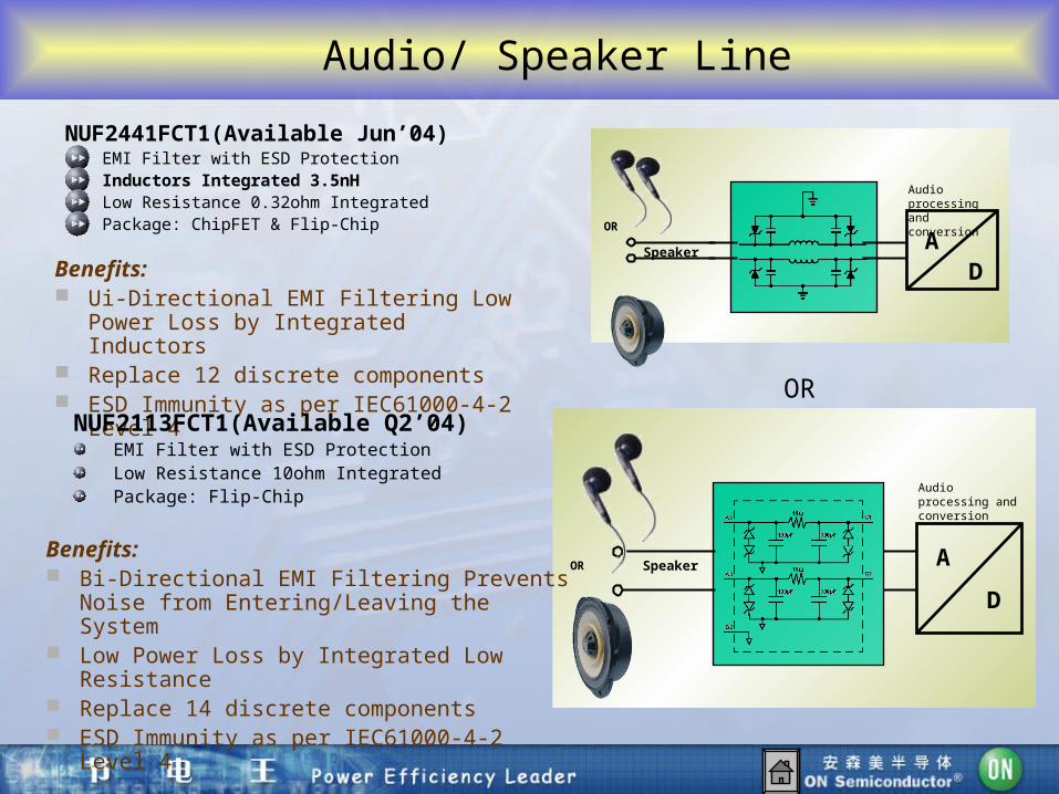
Audio/ Speaker Line
NUF2441FCT1(Available Jun’04)EMI Filter with ESD ProtectionInductors Integrated 3.5nH Low Resistance 0.32ohm IntegratedPackage: ChipFET & Flip-Chip
Benefits: Ui-Directional EMI Filtering Low Power
Loss by Integrated Inductors Replace 12 discrete components ESD Immunity as per IEC61000-4-2 Level
4
Speaker
Audio processing and conversion
AD
Speaker
Audio processing and conversion
A
D
OR
OR
NUF2113FCT1(Available Q2’04)EMI Filter with ESD ProtectionLow Resistance 10ohm IntegratedPackage: Flip-Chip
Benefits: Bi-Directional EMI Filtering Prevents Noise from
Entering/Leaving the System Low Power Loss by Integrated Low Resistance Replace 14 discrete components ESD Immunity as per IEC61000-4-2 Level 4
OR

Headset (Speaker + Microphone)
NUF2114FCT1EMI Filter with ESD ProtectionIntegrated SolutionPackage: Flip-Chip
Benefits: Bi-Directional EMI Filtering Prevents Noise from
Entering/Leaving the System Low Power Loss by Integrated Low Resistance Replace 14 discrete components ESD Immunity as per IEC61000-4-2 Level 4
Audio processing and conversion
A
D

NMF3501FC & NMF3502FC-75dB @ 80MHz -1GHz-60dB @ 1GHz – 2GHzTwo-stage Integrates Filter for Microphone Inputs with Resistors for Biasing, and ESD ProtectionPackage: Flip-Chip
Benefits: Low PCB area (1.2 x 1.7 mm2) Very thin package (0.65mm) Replace 30 discrete components ESD suppression on both input and output
pins (IEC61000-4-2 Level 4)
Microphone
Audio processing and conversion
A
DNMF3501FC NMF3501FC
Stage-1 Stage-2
Audio Line

NZMM7V0T4
9 EMI/RFI Bi-Directional “Pi” Low Pass Filter
4 x 4 mm Lead Less MLF Surface Mount Package
Replace 30 discrete components
Package: 24 PIN MLF
NZF220DFT1
Dual EMI/RFI Bi–directional “Pi” Low–Pass Filters
Package: SC-88A
NZF220TT1
Single EMI/RFI Bi–directional “Pi” Low–Pass Filters
Package: SC-75
ON’s FilterCPU
I1
I2
I3
I7
I8
I9
O1O2
O8O9
O3
O7
Benefits: Suppresses EMI/RFI Noise in Systems Subjected
to Electromagnetic Interference Small Package Size Minimizes Parasitic
Inductance, Thus a More “Ideal” Low Pass Filtering Response
Keypad

Bottom Connector
NUF4105FCT1; NUF6105FCT1; NUF6106FCT1([email protected])4 & 6 Channel EMI Pi-Filter with ESD ProtectionTwo Bump Sizes Available
– 300m(PB) for NUF4105FC and NUF6105FC– 350m(PB-free) for NUF4115FC and NUF6115FC
Package: Flip-Chip
Benefits: Low PCB area Reduced components count Wide freq. range rejection -35dB from 800MHz to 2.2GHz Low line capacitance for high data rate exchange
NUF9001FCT1G10 Channel EMI Pi-Filter with ESD ProtectionTwo Bump Sizes Available
– 300m & 350mPackage: Flip-Chip
Benefits: Low PCB area (2.6mm x 2.6mm) Reduced components countLow line capacitance for high data rate exchange
NUF9001FC
Con
trol
ler
NUF6105/6106NUF4105
Con
trol
ler

NUF4105FCT1; NUF6105FCT1; NUF4115FC; NUF6115FC4 & 6 Channel EMI Pi-Filter with ESD ProtectionTwo Bump Sizes Available
– 300m for NUF4105FC and NUF6105FC– 350m for NUF4115FC and NUF6115FC
Package: Flip-Chip
Benefits: Low PCB area Reduced components count Wide freq. range rejection -35dB from 800MHz to 2.2GHz Low line capacitance for high data rate exchange
NUF9101FCT110 Channel EMI Pi-Filter with ESD ProtectionTwo Bump Sizes Available
– 300m & 350mPackage: Flip-Chip
Benefits: Low PCB area (2.6mm x 2.6mm) Reduced components countLow line capacitance for high data rate exchange
CP
U
NUF6105/15
NUF4105/15
CP
U
NUF9101FC
LCD Display

LCD Display
NUF4105FCT1; NUF6105FCT1; NUF6106FCT1 (20pF@ 2.5V)4 & 6 Channel EMI Pi-Filter with ESD ProtectionTwo Bump Sizes Available
– 300m for NUF4105FC and NUF6105FC– 350m for NUF4115FC and NUF6115FC
Package: Flip-Chip
Benefits: Low PCB area Reduced components count Wide freq. range rejection -35dB from 800MHz to 2.2GHz Low line capacitance for high data rate exchange
NUF4401 or NUF4402
NUF4105/15
NUF4401MNT1,NUF4402,NUF8401 (Available Jul’04)4 and 8 Channel EMI Pi-Filter with ESD Protection100/200 Ohms line resistor design for LCD applicationPackage: NUF4401: 2X2mm QFN package NUF4402: 1.6X1.6mm QFN packageNUF8401: 1.6X4.0mm QFN package
Con
trol
ler
NUF8401
Con
trol
ler

Mega pixel Camera Interface
NUF6106FCT1 (21pF@ 2.5V)6 Channel EMI Pi-Filter with ESD ProtectionLow Capacitance ([email protected]) for Mega pixel/ high speed dataline Package: Flip-Chip
Benefits: Low PCB area Reduced components count Wide freq. range rejection -25dB from 800MHz to 2.2GHz Low line capacitance for high data rate exchange
CP
U
NUF6106FC
CA
ME
RA

Vcc
SIMDATA
SIMCLK
SIMRST
in1
in2
in3
out1
out2
out3
NUF3101FCT1
SIM Card Interface
NUF3101FCT1(Available in Jun 04) Integrated Filter with ESD Protection 3 channels are dedicated to data lines and 1
channel is for the supply voltage Package: Flip Chip (1.6X1.6mm)

Multimedia Card Interface
NUF4105FCNUF4115FC
in1
in2
in3
out1
out2
out3GND
Vcc
Vcc
MMCDATA
MMCCLK
MMCCMD
NZMM7V0T49 EMI Bi-Directional “PI” Low Pass FilterPackage: 24 PIN MLF
NUF4105FCT1; NUF4115FC4 Channel EMI Pi-Filter Array for Data Lines with ESD Protection
Two Bump Sizes Available
– 300m for NUF4105FCT1– 350m for NUF4115FC
Package: Flip-Chip
Benefits: Low PCB area Reduced components count Wide frequency range rejection -35dB from 800MHz to 2.2GHz Low line capacitance for high data rate exchange
Benefits: Low PCB area Reduced components count Low parasitic inductance, providing a more ideal low pass filtering response

Multimedia Card Interface
NUF3101FC
in1
in2
in3
out1
out2
out3GND
Vcc
Vcc
MMCDATA
MMCCLK
MMCCMD
Benefits: Low PCB area Reduced components count Wide frequency range rejection
-30dB @ 800mHz - 1GH-25dB @1GHz – 2GHz
Low line capacitance, 20pF typical, for high data rate exchange
NUF3101FCT1 Integrated Filter with ESD
Protection 3 channels are dedicated to data
lines and 1 channel is for the supply voltage
Package: Flip Chip @ 300um

NUF3101FCT1 Integrated Filter with ESD Protection 3 channels are dedicated to data lines and 1
channel is for the supply voltage Package: Flip Chip
Vcc
SIMDATA
SIMCLK
SIMRST
in1
in2
in3
out1
out2
out3
NUF3101FCT1
SIM Card Interface
Benefits: Low PCB area Reduced components count Wide frequency range rejection -35dB from 800MHz to 2.2GHz Low line capacitance for high data rate exchange

NUF9001FCT1 –10 channel EMI filter
DescriptionThis device is a 10 line EMI filter array for wireless applications. Greater than -35 dB attenuation is obtained at frequencies from 800 MHz to 2.2 GHz. It also offers ESD protection – clamping transients from static discharges. ESD protection is provided across all capacitors.
Features EMI Filtering and ESD Protection 10 line in Flipchip Moisture Sensitivity Level 1
Schedule Phase 0 approved Approved Engineering Sample Now Production Now
Applications•Wireless Phones•Handheld Products•LCD Displays
NUF9001FCT1
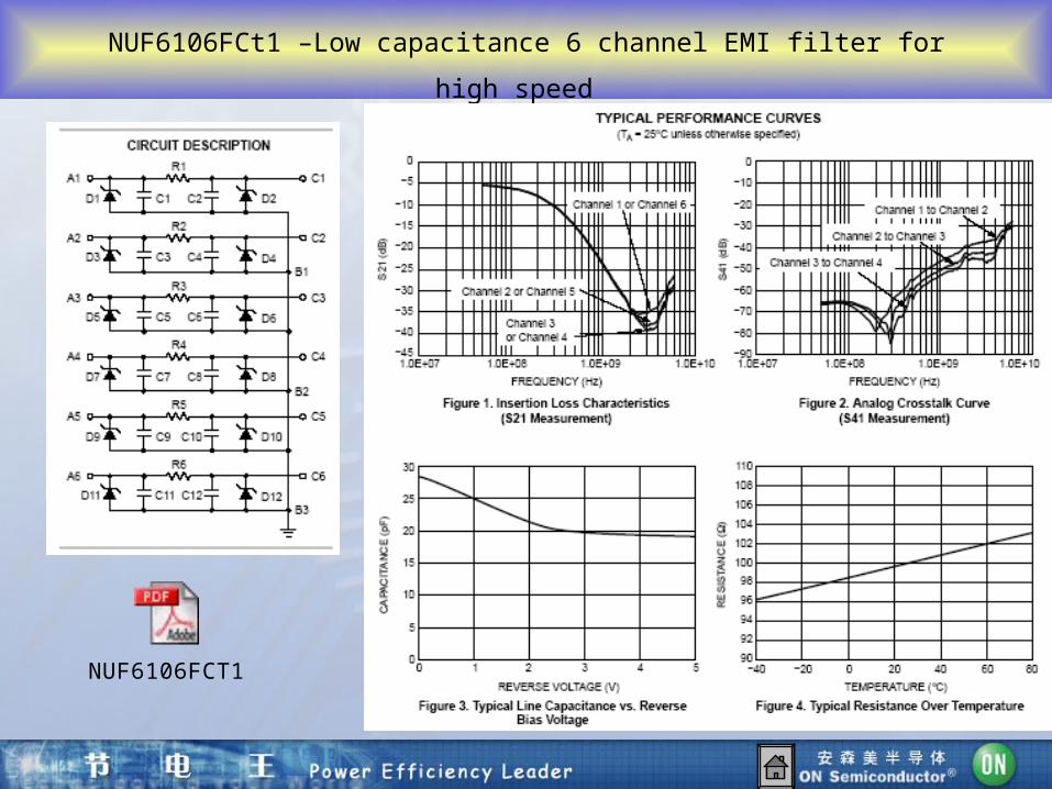
NUF6106FCt1 –Low capacitance 6 channel EMI filter for high speed
NUF6106FCT1

Importance of the parasitic inductance
RS
C
LS
C = 33 pFRs = 0.4 -40
-35
-30
-25
-20
-15
-10
-5
0
10 100 1000 10000
F (MHz)
S2
1 (
dB
)
Ls = 900 pH
Ls = 500 pH
Ls = 100 pH
Lower parasitic inductance enable broadband filtering Equivalent circuit of discrete capacitor
QFN/DFN MicroLeadless
800 pH 500 pH 100 pH 50 pH
Discrete capacitor
Leaded package
Flip chip bumped die

NUF4402 4 Channel filter Smallest 4 line filter Sample available : NOW Production schedule: Aug 04
NUF8401• 8- line EMI filter • 1st 8 line filter in DFN package• Sample available : Aug 04• Production schedule: Sep 04 CMD 8 line Flip chip (1.5X4.0mm)
NUF4401• 4 Channel filter • Standard 8 leaded QFN pacakage• Sample available: NOW• Production schedule: Aug 04
NUF4402• 4 Channel filter • Smallest 4 line filter in QFN
package• Sample available : Aug 04• Production schedule: Sep 04
NEW Products
NUF8401 NUF4401 NUF4402
1.6 X4.0mm
2.0 X2.0mm1.6 X1.6mm

PROS and CONS (QFN versus Flipchips)
QFN package Better Reliability and robust package
Better ESD rating and handling capability
All pins accessible after board mounted for debugging or trouble shooting for design engineers
Better Filter characteristics than Flip-chip or CSP
50% Less parasitic Inductance than Flip-chip or CSP
Increase chip mount density (400um chip to chip separation)
Competitive Pricing

Importance of the parasitic inductance
RS
C
LS
C = 33 pFRs = 0.4 -40
-35
-30
-25
-20
-15
-10
-5
0
10 100 1000 10000
F (MHz)
S2
1 (
dB
)
Ls = 900 pH
Ls = 500 pH
Ls = 100 pH
Lower parasitic inductance enable broadband filtering
Equivalent circuit of discrete capacitor

Pin to Pin Compatibility
Flip chip or BGA (1.33X 3.0mm)
DFN package (1.35X3.0mm)
The DFN package• Pin to Pin replacement• Compatible Foot print • Same Case size Related Part# areNUF6401 and NUF6402

Benchmarking

EMIF10-LCD01F1 EMIF10- COM1 NUF9001FCT1 Unit Remarks
VBR 8 8 7 V IR=10mA
IR500 500 100 nA
Leakage Current @ VR = 3 V
R I/O 100 200 200 Ω
Capacitance 35 45 45 pF Line Capacitance
100 MHz -6dB -12dB -12dB
200 MHz -10dB -17dB -17dB
300 MHz -14dB -22dB -22dB
900 MHz -25dB -35dB -35dB
1800 MHz -27dB -37dB -37dB
Channel 10 10 10
ESD Standard IEC61000-4-2 Air Discharge +-15KVIEC61000-4-2 Contact Discharge +-8KV
Package FilpChip FilpChip FilpChip
PCB area 2.6*2.6mm hight=0.6mm 2.6*2.6mm hight=0.6mm 2.6*2.6mm hight=0.6mm
Ball side

• The driver is activated with + logic voltage/current.
• The driver controls the coil of the relay.
• The integrated Zener diodes protect the FET from the inductor’s kick back when it is deactivated.
• The relay controls the power lines through its contacts.
ON Semi’s device
VCC
uP
VDD
Relay/Motor
Ch1 – VGS
Ch2 – ID
Ch3 - VDS
Vibrator : Vibrator : Integrated Inductance Load Driver
SOT-23

NUD3105/MDC3105Inductive Load Driver
Description NUD3105 is a MicroIntegration™ device designed to provide a robust driver interface between sensitive control circuits and inductive DC loads. It is optimized to drive relays and other loads from a 3V to 5V rail, and can drive relay coils up to 2.5 watts at 5V.
Benefits Efficient and easy interface to control logic Reliable, robust performance Replaces 3 to 6 discrete devices; saves board space Eliminates the need for a separate diode across the load No need to prevent this possibility with extra components
Applications Telecom line cards, modems, fax, answer machines Vibrator driver for cell phones and pagers Desktop computers, peripherals, copiers Consumer electronics, set top boxes Small appliances, white goods Security systems, ATE Solenoid driver Automotive relays, motor controls, lamp drivers
Features Low input drive current Back-to-front transient isolation is inherent Single package integration Integrated free-wheeling diode Guaranteed OFF state if input connection is lost
More Information Online See http://www.onsemi.com/
– Datasheet: NUD3105/D– Case outline– Samples
Ordering Information NUD3105LT1 SOT23 3kU/reel
SOT-23 NUD3105 – MOSFET Drive MDC3105 – Bipolar Drive
Replace 5 discrete!

Power Devices Focus Area
30 1400200-250 600 80060 100 500 900
5
20
15
10
25
30
35
>40
Cellular phone
Handheld productsDC-DC converter,Notebook PC
PC Motherboard
VRM
Automotive powerSteering
DC 48V input DC-DC converter,Color monitor image correction switch
OA equiments,Automotive parts (motor solenoid
driver,DC12-24V
input DC-DC)
Back-up Power Supply
Inverter for Lighting
AC adapter(Notebook, Portable
VCD,DVD)
AC200V power supply
Color monitor(high voltage circuit)
AC100V SMPS
Drain Current (A)
VDS (V)
Focus area

• HD3E & HD3E-RP (1-60V): • Low voltage planar technology: Figure of Merit equals Low RDS(ON) verses low
gate charge. Best for quick switching applications.低压平面技术:特性为低 RDS(ON) 和低栅极电荷。最适合快速开关应用
• TRENCH (1-30V): 沟道 (1-30V)
• Low voltage trench technology: Figure of Merit equal Low RDS(ON) verses die size. Best for lowest RDS(ON) applications.低电压沟道技术:特性为低 RDS(ON) 和小芯片尺寸。最适合低 RDS(ON) 的应用
• HD-Plus (1-250V): • Low and Medium voltage planar technology: Combines the use of MOSFET cells
with poly resistors, capacitors, diodes and logic MOSFETs. Create simple analog circuits. For smart discretes.低压中压平面技术:把 MOSFET 单元和聚酯电阻,电容,二极管和逻辑MOSFET 相结合。建立简单的模拟电路。高性能分立元件。
Power Products Processes功率产品工艺

MOS Power Process Roadmap
1Q02 2Q031Q032Q02 3Q02 4Q02 3Q03 4Q03
Pro
du
ct P
ort
folio
s
Market Segments
Trench 30 V N/P Ch • Computing
Trench 20V N-Ch • Portable & Battery
Trench
HD3E - 20 to 30 V, N & P Ch •Portables/Wireless•Computing
HD Plus
Trench
•Automotive•Computing
TMOS 7 - 40 to 250V, N & P Ch •Automotive•Computing
•Portable & Wireless
•Portable & Wireless
8V P-Channel
20V P-Channel
ProductionQ1 RTM
Development

0
0.5
1
1.5
2
2.5
3
10 100 1000
Cell Density (MCells / in2)
Eff
ec
tiv
e C
ha
nn
el D
en
sit
y (
um
/ u
m2
)
Square Stripe
Figure 1
ON Semi
Competitors Today
World Class Performance using Square Cell
Competitorsrecent
announcements
We offer the industry’s leading RDS(ON) because we have highesteffective channel density

New MOSFET in TSOP6/SOT23 Package
Maximum Ratings
Part VDS VGS ID Type
Number (V) (V) VGS= 4.5V VGS= 2.5V VGS= 1.8V (A)SOT23
* NTR4502PT1 -30 ±20 0.350 0.175 - 1.95
* NTR4101P -20 ±8 0.050 0.060 0.800 2.40
* NTR2101P -8 ±8 0.050 0.065 0.100 3.50
* NTR4503N 30 ±20 0.140 - - 2.50
* NTR4103N 20 ±8 0.040 0.050 0.120 2.40
NTR4501N 20 ±8 0.080 0.100 0.140 2.40TSOP6 SINGLE
* NTGS4111P -20 ±8 0.040 0.050 0.120 3.20
* NTGS2101P -8 ±8 0.026 0.035 0.046 5.60p-
p-
n-
* Trench
TSOP-63.0 X 3.0 mm
SOT-233.0 X 3.0 mm

MOSFET in SC75/SC89/SOT563 Package
Maximum Ratings
Part VDS VGS ID Type
Number Package (V) (V) VGS= 4.5V VGS= 2.5V VGS= 1.8V (A)SINGLE
* NTA4151P SC75 -20 ±8 0.800 1.200 1.800 0.30
* NTE4151P SC89 -20 ±8 0.800 1.200 1.800 0.30
* NTZS3151P SOT563 -20 ±8 0.175 0.240 0.300 0.77
* NTA4153N SC75 20 ±8 0.600 0.700 1.000 0.50
* NTE4153N SC89 20 ±8 0.600 0.700 1.000 0.50
* NTZS3154P SOT563 20 ±8 0.400 0.700 1.000 0.67
NTA4001N SC75 20 ±8 3.000 3.500 - 0.50DUAL
* NTZD3152P SOT563 -20 ±8 0.750 1.000 1.500 0.60COMPLEMENTARY
-20 ±8 0.600 1.000 1.500 0.40 p-
20 ±8 0.400 0.700 1.000 0.40 n-
p-
SOT563* NTZD3155C
p-
n-
* Trench
SC-751.6 X 1.6
mm
SC-891.6 X 1.6
mm
SOT-5631.6 X 1.6
mm

MOSFET in SC88 PackageMaximum Ratings
Part VDS VGS ID Type
Number Package (V) (V) VGS= 4.5V VGS= 2.5V VGS= 1.8V (A)SINGLE
* NTJ S4151P SC88 -20 ±12 0.110 0.145 0.200 0.80
* NTS4101P SC70 -20 ±12 0.400 0.450 0.650 0.80
* NTJ S3151P SC88 -12 ±8 0.060 0.090 0.160 0.92
* NTS2101P SC70 -8 ±8 0.230 0.315 0.400 0.92
NTS4001N SC70 30 ±20 1.200 2.200 4.000 0.50 n-DUAL
* NTJ D4152P SC88 -20 ±8 0.260 0.500 1.000 1.00
* NTJ D2152P SC88 -8 ±8 0.300 0.460 0.900 0.78
NTJ D4001N SC88 30 ±20 1.400 2.600 - 0.25
NTJ D4401N SC88 20 ±12 0.375 0.440 - 0.63COMPLEMENTARY
-8 ±8 0.300 0.400 0.600 0.40 p-
20 ±12 0.385 0.630 - 0.40 n-LOAD SWITCH
-8 ±8 0.300 0.400 0.600 0.40 p-
20 n-
p-
SC88
* NTJ D1155L SC88
* NTJ D4105C
p-
n-
* Trench
SC-882.0 X 2.0 mm
SC-702.0 X 2.0 mm

MOS POWER New Products in ChipFET PackageMaximum Ratings
Part VDS VGS RDS(on) () ID Type
Number (V) (V) VGS= 10V VGS= 4.5V VGS= 2.5V VGS= 1.8V (A)
SINGLE
* NTHS2101P -8 ±8 - 0.025 0.036 0.048 5.4
* NTHS4101P -20 ±8 - 0.034 0.040 0.052 6.7
NTHS5441 -20 ±12 - 0.055 0.083 - 5.3
NTHS5443 -20 ±12 - 0.065 0.110 - 4.7
* NTHS4111P -30 ±20 - 0.042 0.070 - TBD
NTHS4501N 30 ±20 0.035 0.055 - - 6.7
NTHS5404 20 ±12 - 0.030 0.045 - 7.2DUAL
* NTHD2102P -8 ±8 - 0.058 0.085 0.160 3.4
* NTHD4102P -20 ±8 - 0.095 0.135 0.210 2.8
* NTHD4401P -20 ±12 - 0.155 0.240 - 3.0
NTHD4502N 30 ±20 0.085 0.143 - - 3.9
NTHD4508N 20 ±12 - 0.075 0.143 - 4.2COMPLEMENTARY
20 - 0.095 0.135 0.210 2.8 p--20 - 0.080 0.115 - 3.1 n-20 - 0.155 0.260 - 2.1 p--20 - 0.080 0.115 - 3.1 n-
FETKY
* NTHD3101F -20 ±12 - 0.095 0.135 0.210 2.8 p-
NTHD4P02F -20 ±12 - 0.155 0.260 - 2.1 p-
NTHD4N02F 20 ±12 - 0.080 0.115 - 3.1 n-
p-
NTHC5513 ±12
n-
n-
p-
* NTHD3100C ±12
* Trench

New MOSFET in Flip-chip Package
Maximum Ratings
Part VDS VGS ID Type
Number (V) (V) VGS= 4.5V VGS= 2.5V VGS= 1.8V (A)FLIP-CHIP BGA
* NTVS4101P -20 ±12 0.065 0.095 - 4.50
* NTVS4111P -20 ±8 0.021 0.024 - 5.50p-
* Trench
Flip Chip1.6 X 1.6 mm2.0 X 2.4 mm
RTM on Q1 05

SSM3J13T SI3441DV NTGS3441 NTHS5441 Unit Remarks
VDS
-12V -20 -20 -20 VDrain-Source voltage
VGSS
±8 ±8 ±12 ±12 VGate-Source voltage
ID
-3.0 -3.3 -2.2 -3.9 A Drain current (DC)
RDS(ON)
VGS= -4V70 100 90 46 mΩ Max
VGS= -2.5V 95 135 120 83 mΩ max
Package SOT23 TSOP-6 TSOP-6 ChipFET
Size 3mmx3mm hight 1mm
3mmx3mm hight 1mm
3mmx3mm hight 1mm
3mmx1.8mm hight 1mm
Pin out
1.Size reduction 1/3
2.More Drain Pin easy layout

SI5443 NTHS5443T1 SI8405 NTVS4101P Unit Remarks
VDS
-20 -20 -12 -20 VDrain-Source voltage
VGSS
±12 ±12 ±8 ±12 VGate-Source voltage
ID
-4.9 -4.9 -3.6 -3.9 A Drain current (DC)
RDS(ON)
VGS= -4.5V65 65 55 52 mΩ Max
VGS= -2.5V110 110 70 72 mΩ Max
PackageChipFET TSOP-6 Micro Foot FilpChip
The same package
Size 3.0mmx1.8mm hight 1.0mm
3mmx3mm hight 1mm
1.6mmx1.6mm hight 0.6mm
1.6mmx1.6mm hight 0.6mm
Pin out
Pin to Pin

Small Outline Packages – SOT23, SC70Package Channel VDSS Vishay AOS Farichild IR ONSOT23 N 30V Si2316DS AO3410 FDN372S IRLML2803 NTR4503N
0.085 0.033 0.050 0.400 0.140
20V Si2314EDS AO3416 FDN339AN IRLML2502 NTR4103N0.033 0.022 0.035 0.045 0.040
P 30V Si2343DS AO3401 FDN360P IRLML5203 NTR4502P0.086 0.065 0.125 0.165 0.350
20V Si2323DS AO3415 FDN304PZ IRLML6402 NTR4101P0.039 0.043 0.052 0.065 0.085
SI2305DS NTR2101P
12V Si2333DS FDN306P IRLML64010.032 0.040 0.050
8V Si2311DS NTR2101P0.045 0.045
SC70 N 30V Si1302DL AO7400 NTS4001N0.700 0.100 1.500
25V Si1304DL0.350
20V SI1300DL AO7408 MMBF2201N2.000 0.070 1.400
P 30V AO74010.200
20V Si1303EDL AO7411 NTS4101P0.430 0.120 0.360
12V Si1307DL0.290
RDS(ON) @ 4.5V

Small Outline Package – TSOP6Package Channel VDSS Vishay AOS Farichild IR ONTSOP6 N-Single 30V Si3434DV AO6400 FDC645N IRLMS1503
0.034 0.033 0.030 0.200
20V Si3460DV AO6408 FDC637AN IRLMS1902 NTGS34460.027 0.016 0.024 0.100 0.045
P-Single 30V Si3483DV AO6403 FDC658P IRF5800 NTGS34550.053 0.058 0.075 0.150 0.170
20V Si3493DV AO6409 FDC604P IRLMS6802 NTGS34430.027 0.045 0.033 0.050 0.065
12V Si3473DV FDC606P IRLMS4502 NTGS34330.023 0.026 0.042 0.075
8V Si3445ADV0.042
N-Dual 30V Si3948DV AO6800 FDC6561AN0.175 0.075 0.145
20V Si3900DV FDC6401N IRF58520.125 0.070 0.090
P-Dual 30V Si3993DV AO6801 FD6506P0.245 0.185 0.280
20V Si3983DV FDC6312P IRF58500.110 0.115 0.135
12V Si3973DV FDC6318P0.087 0.090
8V Si3905DV0.125
P+N 30V Si3552DV AO6601 FDC6333C0.360+0.175 0.185+0.075 0.220+0.150
20V Si3586DV AO6604 FDC6420C IRF58510.110+0.060 0.110+0.060 0.125+0.070 0.135+0.090
Loadswitch 20V Si3861DV FDC6330L NTGS1100L0.175 0.125 0.080
12V Si3863DV0.105
8V Si3865DV FDC6331L0.060 0.055
RDS(ON) @ 4.5V

Small Outline Packages – SC88Package Channel VDSS Vishay AOS Farichild IR ONSC88 N-Single 30V Si1426DH FDG315N
0.115 0.160
25V Si1404DH FDG313N NTJS4405N0.350 0.450 0.350
20V Si1406DH FDG327NZ0.065 0.090
P-Single 30V Si1433DH AO7405 FDG316P0.260 0.200W 0.300
20V Si1413DH FDG326P NTJS4151P0.115 0.140 0.095
12V Si1417DH FDN306P NTJS3151P0.085 0.040 0.060
8V Si1405DL0.125
N-Dual 30V Si1900DL ^FDG6303N NTJD4001N0.700 0.450 1.500
20V Si1912EDH AO7800 FDG6335N NTJD4401N0.280 0.235 0.300 0.375
P-Dual 30V ^FDG6304P1.100
20V Si1913EDH AO7801 FDG6308P NTJD4152P0.490 0.520 0.400 0.260
12V Si1917EDH FDG6316P0.370 0.270
8V Si1905DL NTJD2152P0.600 0.300
P+N 30V Si1539DL ^FDG6321C1.700+0.700 1.100+0.450
20V Si1563EDH AO7600 FDG6332C0.490+0.280 0.520+0.235 0.420+0.300
12V Si1557DH0.535+0.235
8V Si1555DL NTJD4105L0.600+0.385 0.375+0.300
Loadswitch 20V FDG6324L NTJD1155L0.750 0.300
12V
8V Si1865DL FDG6331L0.215 0.260
RDS(ON) @ 4.5V

Benefits Previously only available in SO-8 package (5 X 6 mm) Higher efficiency, reduced battery drain. Less voltage drop across the diode.
Features New smaller ChipFET™ in 8 lead package (1.9 X 3.0 mm) P-Channel MOSFET, VDDS= 20V, RDS(on)=130mΩ @ VGS = 4.5V SCHOTTKY VR=20V, with Low VF =0.32V @ 1 Amp
More Information Online See www.onsemi.com for:
– Datasheet –Case outline
Anode
Anode
Source
Gate
Cathode
Cathode
Drain
Drain
Description
Ultra-small eight lead package allows the integration of a MOSFET and Schottky Rectifier into one package. This is the smallest FETKY™ on the market with a maximum footprint of 3.10 X 2.00 mm to optimize board space. Independent pin out to each device to increase design flexibility, i.e. use Schottky as blocking diode or in parallel with body diode.
Applications
Any handheld application, including Cellular phones, Digital Cameras, MP3s, and PDAs that requires DC-DC converters (buck, buck-boost, and synchronous rectification).Charge control in portables
Product Availability: Samples Now Production Jan/03
NTHD4P02FT(135mohm / NTHD3101(95mohm)-FETKY™ MOSFET Plus Schottky Rectifier
NCP1800
Rcomp
Ccomp Cout
NTHD4P02F
ISNSVSNS
ISEL
Vcc
CFLGCOMP/DIS
OUT
Gnd
Vin
Host or LedHost Processor
CinRisel60K
Rsns
FETKy

Power Management (Charging) 电源管理
Schottky Rectifiers (Reverse current protection)Powermite MBRM120LT3 20V 0.45V@1A
MBRM120ET3 20V 0.53V@1A (Low leakage)MBRM130LT3 30V 0.45V@1A
SOD123 MBR0520LT3 20V [email protected]
Signal MOSFETsTSOP-6 NTGS3441 3.3A [email protected]
NTGS3443 3.1A [email protected]
ChipFET NTHS5441 3.9A [email protected] NTHS4101P 4.8A [email protected]
FETky (MOSFET/Schottky/ 肖特基 )
ChipFET NTHD4P02F 20V, 1.0A [email protected]
NTHD3101F 20V, 1.0A [email protected]
MBR0520 (20V,0.5A) SOD123 Schottky
MBRM120 (20V,1A) SOD123 Schottky

FETky Applications
Boost using N-Channel FETKy NTHD4N02FT1
NTHD4N02F
Buck using N-Channel FETKy NTHD4N02FT1
Vo
PWMControl
Vin
NTHD4N02F
Charging Circuit using P-Channel
NCP1800
Rcomp
Ccomp Cout
NTHD4P02F
ISNSVSNS
ISEL
Vcc
CFLGCOMP/DIS
OUT
Gnd
Vin
Host or LedHost Processor
CinRisel60K
Rsns
FETKy
Buck using P-Channel
NTHD4P02F

High Side Power Management - Load Switch
Application:Combines level shift with power switch Uses small N-Ch to drive large P-Ch Reduces board space Targeting trench and smaller packages
Trench products will combine small N-Ch with Large P-Ch
Products:NTHC5513, ChipFET, Complementary, 20V N&PNTJD4101C, SC-88, Complementary, 20V N & 8V PNTJD4105C, SC-88, Load Switch, 20V N & 8V PFor discrete see next page

High Side Load Switch高端负载开关
Switch is used in Positive side of Power Supply开关用在电源的正极
The lower the RDS(on) the higher the system efficiencyRDS(on) 越低,系统效率越高
Package vary depending on current applied封装随着应用的电流改变
Solution:解决方案 ON Semiconductors P-Channel trench provides lowest RDS(ON) in Industry
安森美半导体的 P- 沟道器件提供业内最低的 RDS(ON) Offering a variety of packages options depending on the current required
根据要求的电流提供各种封装选择
Device 器件 Package 封装 Key Parameter 主要参数Samples 样品Release 发布NTHS2101PT1 ChipFET 8V, 25 [email protected] Now 现在 Now 现在NTHS4101PT1 ChipFET 20V, 34 [email protected] Now 现在 Now 现在NTGS4111PT1 TSOP-6 20V, 40 [email protected] Oct 十月 Q1 04 2004 年 1 季度NTR2101PT1 SOT-23 8V, 50 [email protected] Sept 九月 Q1 -04 2004 年 1 季度NTR4101PT1 SOT-23 20V, 55 [email protected] Dec 十二月 Q1-04 2004 年 1 季度NTVS4101PT1 FlipChip 20V, 65 [email protected] Dec 十二月 Q1-04 2004 年 1 季度NTJS3151PT1 SC-88 12V, 75 [email protected] Dec 十二月 Q1-04 2004 年 1 季度NTJS4151PT1 SC-88 20V, 110 [email protected] Dec 十二月 Q1-04 2004 年 1 季度NTS2101PT1 SC-70 8V, 230 [email protected] Dec 十二月 Q1-04 2004 年 1 季度NTS4101PT1 SC-70 20V, 400 [email protected] Dec 十二月 Q1-04 2004 年 1 季度NTZS3153PT1 SOT-563 20V, 600 [email protected] Jan 一月 Q1-04 2004 年 1 季度
Inputs from:
•Battery
•Switching Regulator
•LDO
•Etc.
(-)
(+)Display
Logic(+)
ASIC(+)
P.A.(+)
PMU

N-Channel Level Shifter N- 沟道电平移动器
Application:应用: Need small N-Ch as level shifter to drive
large P-Ch需要小型 N- 沟道作为电平移动器来驱动大型P- 沟道
N-Ch has low current requirementN- 沟道要求小电流
Targeting Smaller packages目标在于更小型封装
Source源极
Drain漏极
P-ChP- 沟道
N-ChN- 沟道Gate
栅极Gate Drive
fromController
or uProcessor
来自控制器或微处理器的栅极驱
动
(+)
(+) Input Volts
(+) 输入电压 L
oad
负载
(+)
Device器件
Package封装
Key Parameter主要参数
Samples样品 RTM
NTA4001N SC-7520V, 2.5Ω@2.5V, ESD Gate20V, 2.5Ω@2.5V, ESD 栅极
Now现在
Now现在
NTS4001N SC-7030V, 1.5Ω@2.5V, ESD Gate30V, 1.5Ω@2.5V, ESD 栅极
Now现在
Now现在
NTJD4001N SC-8830V, 1.5Ω@2.5V, ESD Gate30V, 1.5Ω@2.5V, ESD 栅极
Now现在
Now现在

Power Management (Load Switch)电源管理(负载切换)
Application:应用:Combines level shift with power switch 结合了电平移位和功率切换 Uses small N-Ch to drive large P-Ch 使用小 N- 沟道来驱动大的 P- 沟道 Reduces board space 减小了板空间 Targeting trench and smaller packages 目标在于沟道和更小的封装
Device器件
Package封装
Key Parameter关键参数
Samples样品 RTM
NTHC5513 ChipFET 20V, 155 [email protected]现在
Now现在
NTJD4105C SC-88 8V, 340 [email protected]现在
Now现在
NTJD1155L SC-88 8V, 150 [email protected]三月
Apr四月
输入 输出
负载电源管理
电池
负载开关
负载开关
负载开关
负载开关
功率放大器
显示器
逻辑器件

NTHC5513T1- ChipFET™ Complementary MOSFET
Benefits优点 40% footprint reduction over TSOP-6 相比 TSOP-6 减小了 40% 的占用面积 Higher efficiency 效率更高 Reduced battery drain 电池消耗更低
Features特性 ChipFET™ is smallest Complementary package to date
ChipFET™ 是目前最小的互补封装 N-Channel MOSFET, VDDS=20V,RDS(on)= 60mΩ @ VGS=4.5V
N- 沟道 MOSFET, VDDS=20V,RDS(on)= 60mΩ @ VGS=4.5V P-Channel MOSFET, VDSS=20V, RDS(on)=130 mΩ @ VGS=4.5V
P- 沟道 MOSFET, VDSS=20V, RDS(on)=130 mΩ @ VGS=4.5V
Description描述This complementary package provides both N-Channel and P-Channel FETs in one IC, it targets customers who want to reduce component count on their designs. 该互补封装在一个 IC 中提供了 N- 沟道和 P- 沟道 FET ,适用于要减少他们设计中元件数量的客户。Independent pin out to each device to increase design flexibility. 独立的引脚输出到每个设备,增加了设计灵活性。The ChipFET™ package offers a maximum footprint of 3.10 X 2.00 mm to optimize board space. ChipFET™ 封装提供了最大 3.10 X 2.00 mm 的占用面积,以优化板空间
Applications应用
Handheld devices, including Cellular phones, Digital Camera, MP3, and PDAs 手持设备,包括手机、数码相机、 MP3 和 PDA DC-DC converter (buck, buck-boost, and synchronous rectification) 直流-直流转换器(降压、降压-升压和同步整流Load Switch for portable applications 便携式应用的负载切换
Vo
PWM ControlPWM 控制Vin
NTHC5513
底视图 顶视图

MOSFET: Battery Pack Roadmap
MC33349NCP802Vcell
GND
Ct
Discharge
Pack +
Charge
Pack -Q1Q2
NTQD6866NTQD6968NNTQD4154Z
20mm2
MMDF7N02
31mm2
Foo
tpri
nt
Time
NTLTD7900Z
11mm2
2.6mm2 x2
NTVS4101Z
2mm width package
8~10 mm2

Battery FET Portfolio
VDSS (V) VGS (V) Typ Max
TSSOP8
NTQD6866 20 ±12 0.025 0.030 N A
NTQD6968N 20 ±12 - 0.022 N B
* NTQD4154N 20 ±12 0.017 0.022 Y B
MICRO8-LL
NTLTD7900Z 20 ±12 0.021 0.026 Y A
2mm package
* NTLXxxxxN 20 ±12 0.017 0.022 Y -
RDS(ON) (m )@VGS =4.5V ESD Protection
Pin Configuration
TSSOP8
Pin Configuration “A” Pin Configuration “B”
Micro8LL
* Trench

Audio Amplifiers
ON Advantage Device can be driven directly off the battery where the competition requires an
additional part. Cancellation circuitry for pop and click noise No output capacitors on the stereo headset amplifier is an advanced feature to reduce
part count.
A = active, S = samplingRTM = release to market
Device Description StatusDemoBoard
NCP2890DMR2 1W mono audio amplifier in a micro 8 A YNCP2890AFCT2 1W mono audio amplifier in a 9-pin Bump A YNCP2809ADMR2 NCP2809BDMR2
135 mW stereo headset audio amplifier (no output capacitors required)
AY
NCP48941W mono audio amplifier with Fully
Differential Inputs, 9-bin uBump/Micro10S
(RTM May 04)
NCP48961W mono audio amplifier with Earpiece Driving Capability, 9-bin uBump/Micro10
S(RTM May 04)
NCP2820 Class D, 2W mono audio amplifier Developmemt

Applications• Wireless phones• PDAs• Portable Electronic Devices• Electronic Toys
Description The NCP2890 is an audio power amplifier capable of delivering 1W of continuous average power to an 8 load from a 5V-power supply, and 320 mW to a 4 load from a 2.6V power supply. The NCP2890 provides high quality audio while requiring few external components and minimal power consumption. It features a low-power consumption shutdown mode, which is achieved by driving the shutdown pin with logic low. The NCP2890 contains circuitry to prevent from “pop and click” noise that would otherwise occur during turn-on and turn-off transitions. For maximum flexibility, the NCP2890 provides an externally controlled gain (with resistors), as well as an externally controlled turn-on and turn-off times (with the bypass capacitor).
More Information Online: www.onsemi.com/ncp2890
Ordering Information • NCP2890DMR2 in Micro8, 4000 per reel• NCP2890FCT1 in Microbump9, 3000 per reel
Features• 1.2 W to an 8 load from a 5V power supply• 520 mW to an 8 load from a 3.3V power supply• 700 mW to a 4 load from a 3.3V power supply• 2.5V – 5.5V operation• Ultra low current shutdown mode• External gain configuration capability• External turn-on and turn-off time configuration capability• Thermal overload protection circuitry• Extremely high performances : PSRR and THD+N• « Pop and click » noise protection circuit• Ultra small Microbump9, Micro8 packages
Benefits• Handfree operations
• Earpiece operations• Operates directly from 1 cell Li+ or 3 cell NiMH batteries.• Extends battery life• Flexibility
• No LDO needed, High quality of sound• User friendly• Saves PCB surface
NCP28901 watt Audio Amplifier

NCP2890 Typical ApplicatonNCP2890 典型应用原理图
音频输入
旁路
关断
关断控制
ON Semiconductor
should be deleted

NCP2890 Output Power vs Supply Voltage
400
600
800
1000
1200
1400
1600
3.0 3.5 4.0 4.5 5.0
Power Supply (V)
Ou
tpu
t P
ow
er (
mW
)
THD+N=1%
THD+N=10%
NCP2890 / Output Power vs Supply Voltage. F=1kHz, RL=8

NCP2890 : Parametric Analysis
NCP2890
LM4890
0,01
0,10
1,00
10,00
0 100 200 300 400 500
Pout (mW)
THD
+N (%
)
THD+N vs. Pout Cbypass=1µF
Vp=2.6V, RL=4, Av=2, F=1KHz
-80
-75
-70
-65
-60
-55
-50
-45
-40
-35
-30
10 100 1 000 10 000
Frequency (Hz)
PS
RR
(d
B)
PSRR vs. VpVp=2.6V, RL=8, Av=2, Rin=10, VRipple=200mVpk-pk
Cbypass=1µF
LM4890
NCP2890
THD+N vs. Pout Cbypass=1µF
Vp=5V, RL=8, Av=2, F=1KHz
0,01
0,10
1,00
10,00
0 200 400 600 800 1000 1200 1400
Pout (mW)
THD+
N (%
)
NCP2890
LM4890
PSRR vs. Vp Cbypass=1µF
Vp=5V, RL=8, Av=2, Rin=10, VRipple=200mVpk-pk
-70
-65
-60
-55
-50
-45
-40
-35
-30
10 100 1 000 10 000Frequency (Hz)
PS
RR
(d
B) LM4890
NCP2890

NCP2890 : Parametric Analysis
Parameter Conditions NCP2890 LM4890 TS4890 TPA6203A1 Unit
Vp=5V, No Load 1.7 4 6 1.7 mA (typ)Vp=5V, 8 Ohms 2.1 5 no data no dataVp=2.6V, No Load 1.5 2.6 5 1.7
Shutdown current 1.0 2 1 0.9 µA (max)Output Offset
Voltage (Low er is better for battery life)
Vp=5V 20 50 20 9 mV (max)
THD+N (distortion)
Vp=2.6V, Av=2, RL=4ohms,F=1khz, Pout=300mW
0.04% 4% 0.2% 0.08%
PSRR (power supply ripple
rejection)
Vp=2.6V, Av=2, RL=8ohms, F=1kHz, Vripple=200mVp-p
-75dB -42dB -77dB -90dB (Av=1), -75dB (Av=5)
Micro8/Msop8 package size
3.0 x 4.9 mm (DMR2
suffix)
3.0 x 4.9 mm (MMX
suffix)
3.0 x 4.9 mm (IST
suffix)
not available
Microbump/BGA package size
1.45 x 1.45 mm (FCT1
suffix)
1.51 x 1.51 mm (IBLX
suffix)
not available
2.0 x 2.0 mm (GQV
suffix)
Quiescent Power Supply current

Applications
Portable stereo MP3 Player Cellular Phone Electronic Toys Personal Computer
Description
The NCP2809 is a cost-effective stereo audio power amplifier capable of delivering 135mWper channel of continuous average power per channel into 16 loads.
The NCP2809 audio power amplifier is specifically designed to provide high quality outputpower from low supply voltage, requiring very few external components. Since NCP2809does not require bootstrap capacitors or snubber networks, it is optimally suited for lowpower portable systems. NCP2809A has an internal gain of 0dB while specific external gaincan externally be set with NCP2809B .
If the application allows it, the virtual ground provided by the device can be connected tothe middle point of the headset. In such case, the two external heavy coupling capacitors areuseless. Otherwise, you can also use both outputs in single ended mode with externalcoupling capacitors.
Due to its excellent PSRR, it can be directly connected to the battery, saving the use of aLDO.
More Information Online: www.onsemi.com/ncp2809
Ordering Information NCP2809ADMR2, Micro10, 4000 per reel NCP2809BDMR2, Micro10, 4000 per reel
NCP2809: NOCAP™ 135mW Stereo Headphone Power Amplifier
Already RTM

NCP2809 Parametric Analysis
0.001
0.01
0.1
1
10
0 20 40 60 80 100 120 140 160
Output Power (mW)
TH
D+
N (
%)
Vp=5V
Vp=3.3VVp=2.4V
THD+N vs.. Pout @ RL=16, f=1kHz
0.001
0.01
0.1
1
10
10 100 1 000 10 000 100 000
Frequency (Hz)
TH
D+
N (
%)
Vp=2.4V, Pout=20mW
Vp=5V, Pout=75mW
Vp=3V, Pout=30mW
THD+N vs.. Frequency @ RL=16
-70
-60
10 100 1 000 10 000 100 000
Frequency (Hz)
Cro
ssta
lk (
dB
)
Vp=2.4V, Pout=20mW
Vp=5V, Pout=75mW
Vp=3V, Pout=30mW
Crosstalk vs. Frequency @ RL=16
-110
-100
-90
-80
-70
-60
-50
-40
-30
-20
-10
10 100 1 000 10 000 100 000Frequency (Hz)
PS
RR
(d
B)
Vp=2.4V
Vp=5V
Vp=3V
PSRR @ Inputs grounded, Vripple=200mV pk-pk, RL=16

NCP2809 Application
:
Turn On sequence : Math2=V(load)=Ch3 -Ch1 Turn On sequence Zoom : Math2=V(load)=Ch3-Ch1
Turn Off sequence : Math2=V(load)=Ch3-Ch1 Turn Off sequence Zoom : Math2=V(load)=Ch3-Ch1
Ch1 = OUT_RCh2 = VMCCh3 = OUT_LMath1 = Vload_R = Ch1 - Ch2Math2 = Vload_L = Ch3 - Ch2

NCP2809A (Int Gain) / B (Ext Gain)
2.2V~5.5V Supply
135mW @ 16Ω 5V
Ultra Low Iq: 0.6µA max
Virtual Ground: Brilliant accuracy
excellent Crosstalk, Iq and offset
“Pop & Click” noise immunity
Excellent PSRR (90dB)
Directly supplied from Vbat
THD+N of 0.007% (typ)
Only 4 External Components for NCP2809A
8 External Components only for NCP2809B
µ10 Package (15mm²)

NCP2809 Benchmark
ON National MaximNCP2809 LM4911 MAX4410
Vcc 2.5V ~ 5.5V 2.0V ~ 5.5V 1.8V ~ 3.6VOutput Power16 Ohms/3V
45mWTHDN=1%
40mWTHDN=1%
80mWTHDN=1%
Iq (Shutdown) 0.6µA 1µA 6µAExternal SD Yes Yes YesPop & Click Yes (brilliant) Yes (partially) YesPSRR 90dB 55dB 90dBVbat -> Vcc Yes No NoTHD+N 0.007% (typ) 0.3% (max) 0.005% (typ)External Components
4 (A version)8 (B version) 7
5 (MAX4411)9 (MAX4410)
Package Type µ10 µ8 µBump/TSSOPPackage Size 15mm² 15mm² 4mm²/30mm²

Applications Cell Phone Portable stereo MP3 Player Electronic Toys Personal Computers
Description
The NCP4894 is a fully differential audio power amplifierdesigned for portable communication device applications. Thisfeature and the excellent audio characteristics of the NCP4894 are aguarantee of a high quality sound, for example, in mobile phonesapplications. With less than 0.01% distortion (THD + N), theNCP4894 is capable of delivering 1.0 W of continuous averagepower to an 8.0 load from a 5.0 V power and still 250 mW from2.6 V.
Ordering Information NCP4894 in µBump-9 and in µ-10
Features Fully Differential 1.2 W to an 8 load from a 5V power supply 2.5V – 5.5V operation Ultra low current shutdown mode External gain configuration capability External turn-on and turn-off time configuration capability Thermal overload protection circuitry Extremely high performances : PSRR and THD+N « Pop and click » noise protection circuit Ultra small Bumped die
Benefits
Drive capability for Polyphonic ringer or Speakerphone Operates directly from 1 cell Li+ or 3 cell NiMH batteries. Extends battery life Flexibility
No LDO needed, High quality of sound User friendly Saves PCB surface
NCP48941 Watt Fully Differential Audio Amplifier
Sample now, MP May 04

NCP4894 Typical Application Schematic NCP4894 典型应用原理图
VMC 桥
SD 选择
SD 模式
旁路
关断控制
旁路
旁路
差动
音
频输
入

NCP4894 Stereo Application Schematic NCP4894 立体声应用原理图
VMC 桥
SD 选择
SD 模式
旁路
关断控制
旁路
旁路
差动
音频
输入

Packaging 9 pin Flip-Chip CSP (1.5x1.5mm)
Product Ordering Information NCP4896FCT1G (9 pin Flip-Chip CSP)
3000 Units Tape and Reel, G suffix stands for Pb-free
Market & ApplicationsCellular Phone, PDA, DSC
DVD Player, Audio/Video Players
Personal Computer, Sound Card
Electronic Toys
Portable mono loudspeaker & earpiece
Features 2.2V to 5.5V operation 1.1W to an 8Ω load from a 5V supply, THD+N<0.008% Ultra Low Shutdown Current (20nA typical) “Pop & Click” noise protection circuit Superior THD+N: 0.007% at 1W Superior PSRR (70dB) Very Few External Components
NCP4896 1W Audio Power Amplifier with Earpiece Driving Capability
Through a dedicated SE/BTL pin, the user can drive either a single-ended 32Ω load (earpiece) up to 90mW, or a bridge-tied 8Ω load (loudspeaker) up to 1W. It saves the need of a second audio amplifier or an analog switch for the earpiece . The NCP4896 provides high quality audio while requiring few external components and minimal power consumption.
Benefits Supports wide range of battery power applications High Output Power Extends Battery Life Excellent Sound Quality Excellent Sound Quality Direct Connection to Battery, Saving an LDO Saves Manufacturing Cost
The NCP4896 is an audio power amplifier designed for portable device applications.

NCP4896 1W Audio Power Amplifier with Earpiece Driving Capability
2.2V~5.5V SupplyThrough a dedicated SE/BTL pin, the user can drive either a single-ended 32Ω load (earpiece) up to 90mW, or a bridge-tied 8Ω load (loudspeaker) up to 1W.
→ Saves the need of a second audio amplifier or an analog switch for the earpiece .
High Output Power:→ 1.1W with 0.008% THD+N @ 8Ω, 5V
Ultra Low shutdown current: → 20nA typical
Very Low quiescent current:→ 2mA typical at BTL (bridge-tied load)→ 1mA typical at SE (single-ended)
“Pop & Click” noise protectionSuperior THD+N of 0.007% @ 1W, 8Ω, 5VVery Low Noise floor: 15µVrms (SE) & 35µVrms (BTL)Excellent PSRR (-70dB):
→ Directly supplied from Vbat. Save a LDO
9 pins Flip-Chip CSP ( 1.5x1.5mm)

White LED Boost Drivers
Device Package Special Attributes Series Parallel StatusEval.
BoardNCP1403 SOT23-5 Low input voltage 1.2V~5.5V. Suits 2-cell Alkaline/NiMH
applications.4 8 A Yes
NCP5007 SOT23-5 High efficiency up to 86%. Suitable for LiIon applications and 3 cell NiMH as well.
5 15 S (RTM Jun 04)
Yes
NCP5008/9 Micro10 Serial data input pin allows LED brightness control by 牌 .Does not need a sense resistor
3-4 10 A Yes
# of LEDs in
Typical Applications
Small Color LCD Screens
Cell phones, Digital Cameras, PDAs, and GPS
Portable electronics and instrumentation
ON Advantage Low end applications: The NCP1403 with low input voltage is suitable for 2-cell Alkaline/NiMH applications. Feature Rich applications: The NCP5009 automatically adjust screen brightness based on ambient light and
provides digital dimming via serial MPU interface Mainstream: NCP5007 with high efficiency > 80% and ability to drive up to 5 LEDs in Series
A = activeRTM = release to market

What about a Charge Pump?
Fig. 1 Efficiency as a function of Battery voltage
2.7v 3.0v 3.3v 3.6v 3.9v 4.2v
90%
60%
Efficiency
Dual mode fractional
charge-pump
Inductive Boost
(NCP5007)
Battery usable range VBAT

Applications Backlight for small color LCD screens High Efficiency Step up converters Portable devices
Description The NCP5007 is a very high efficiency boost converter operating in current loop control mode to drive Light Emitting Diode. The current mode regulation allows a uniform brightness of the LED’s.
Ordering Information NCP5007SNT1G SOT23-5 T&R Units 3000
Features Inductor based converter
Built-in over-voltage protection 2.7 to 5.5V Input voltage range Vout up to 22V 1µA Quiescent Supply Current Includes dimming function by PWM on
either enable pin or feedback pin Only 5 external components High frequency switching mode Zero cross switching at no current
Benefits Brings higher efficiency up to 86%
(10 to 20% higher than charge-pump) Saves a zener diode at output pin Operates directly from 1 cell Li+ or 3 cell NiMH batteries Allowing up to 5 LEDs in series or 15 as a total. Extends battery life For smooth brightness changes
Lowest part count and easier design Allows small inductor (22uH) Low noise DC/DC converter, Reduces EMI
NCP5007Compact White LED Boost Driver
More Information Online: http://www.onsemi.com/ncp5007
RTM June 04

Description The NCP5007 is a very high efficiency boost converter operating in current loop control mode to drive Light Emitting Diode. The current mode regulation allows a uniform brightness of the LED’s.
Features 2.7 to 5.5V Supply voltage Up to 85% efficiency Vout up to 22V (5 LEDs in series) Over-voltage protection Thermal protection 3µA Quiescent Supply Current Shutdown control Only 5 external components High frequency switching mode Low noise operation Vcc independent from Vbat SOT23-5 package Dimming function by PWM on EN or FB pins
NCP5007Compact White LED Boost Driver
Inductor supply can be higher than Vcc
Low 0.2V reference voltage minimizes the efficiency loss in R1
Built-in Overvoltage Protection, saves a
Zener

Features:• Vout up to 15V@20mA with Vin>2.7V, or 10V@20mA with Vin>1.8V • Uniform brightness through series configuration
1F
RN = 0.8V/20mA = 40 ohm,
Pdiss = R.(20mA)² = 16mW
NCP1403(SOT23-5)
NCP1403White LED Boost Driver (suitable for low Vin)

Applications Backlight for small color LCD screens High Efficiency Step up converters Portable devices
Description The NCP5007 is a very high efficiency boost converter operating in current loop control mode to drive Light Emitting Diode. The current mode regulation allows a uniform brightness of the LED’s.
More Information Online: TBD
Ordering Information TBD SOT23-5 T&R Units 3000
Features Inductor based converter Built-in over-voltage protection 2.7 to 5.5V Input voltage range Vout up to 22V 1µA Quiescent Supply Current Includes dimming function by PWM on
either enable pin or feedback pin Only 5 external components High frequency switching mode Zero cross switching at no current
Benefits Brings higher efficiency (up to 83%) than charge-pump Saves a zener diode at output pin Operates directly from 1 cell Li+ or 3 cell NiMH batteries Allowing up to 5 LEDs in series or 15 as a total. Extends battery life For smooth brightness changes
Lowest part count and easier design Allows small inductor (22uH) Low noise DC/DC converter, Reduces EMI
NCP5007*Compact White LED Boost Driver
*Coming soon

NCP5007*Application Circuit
*Coming soon
Built-in over-voltageProtection Saves aZener diode at Vout pin.

NCP5007*: Additional information
*Coming soon

White LED: Competitor Parametric AnalysisCompetitor Maxim MPS National TI Toko
Part number MAX1848 LT1932 LT1937 MP1523 LM2703 TPS61040 TK11850 NCP1403 NCP5007
LED brightness control
Analog or DAC Control
PWM PWM PWM PWM PWM PWM PWM PWM
Automatic brightness control
NO NO NO NO NO NO NO NO NO
Package SOT23-8 SOT23-6 SOT23-5 SOT23-5 SOT23-5 SOT23-5 SOT23L-8 SOT23-5 SOT23-5
Package Size 3x3 mm 3x3 mm 3x3 mm 3x3 mm 3x3 mm 3x3 mm 3.3x3.5 mm 3x3 mm 3x3 mm
Regulation Mode CURRENT CURRENT CURRENT CURRENT CURRENT CURRENT CURRENT CURRENT CURRENT
Sense Resistor EXTERNAL INTERNAL EXTERNAL EXTERNAL EXTERNAL EXTERNAL EXTERNAL EXTERNAL EXTERNAL
Total Passive Part Count
6 6 6 6 6 6 7 6 5
Input Voltage 2.6 to 5.5V 1 to 10V 1 to 10V 2.7 to 25V 2.2 to 7V 1.8 to 6V 2.3 to 10V 1.2 to 5.5V 2.7 to 5.5V
Output voltage up to 13V up to 36V up to 36V up to 25V up to 21V up to 28V up to 20V up to 15V up to 22V
Over-voltage protection
YES NO NO NO NO NO NO NO YES
Max number of LEDs in series
3 8 6 6 4 6 4 4 5
Max number of LEDs in parallel
6 ? ? ? ? ? ? 10 15
Feedback voltage NA (1) NA (1) 0.1V 0.4V 1.2V 1.2V 0.5V 0.8V 0.2V
Efficiency (2) @ Vin=3.6V, 3LEDs (series), 15mA
83% 78% 82% 82% 75% 75% 73% 72% 83%
Switching frequency
1.2MHz 1.2MHz 1.2MHz 500KHz 1MHz 1MHz 800kHz 300kHz 600kHz
Inductor value 33uH 6.8uH 22uH 10uH 10uH 10uH 22uH 22uH 22uH
Shutdown current 0.3µA 0.1µA 0.1µA 1µA 0.1uA 0.1uA 0.1uA 0.3µA 1µA
Price High High High Medium Medium Medium Medium Medium Medium
Selling points
Vin below 2V => suits 2-cell Alkaline/NiMH applications
High eff iciency
83%, Over-voltage
protection
Linear Tech ON
Note: (1) 'NA' = not applicable. (2) Eff iciency = LED output pow er / Input pow er.

25V low side switch, 1.2V Feedback Voltage
Max output current: 50mA @ Vout=15V, 25mA @ Vout=25V
85% Efficiency at Vout = 25 V, Iout = 25 mA, Vin = 5.0V
85% Efficiency at Vout = 15 V, Iout = 50 mA, Vin = 5.0V
Low Operating Current of 15 uA (Not Switching)
Ceramic Capacitors
PFM switching up to 1MHz
25 VC2
4.7FC3C1
10F
R1
Enable
R2
NC
P
1
2
3
5
4
CE
FB
VDD GND
LX
VIN VOUT
L 4.7 H D MBRM130LT1
1.8 V to 5.5 V
5 pF to 150 pF
C4
150pF
Applications• Cell Phone OLED Driver• PDAs• Digital Cameras• Handheld Games• Portable Audio
Sample now, MP June 04
NCP1406 25V PFM Step-Up DC-DC Converter for OLED Bias

New Flash Concept – Ultra Bright White LED
Casio SonyEricsson
White LED
Sanyo

Flash LED Suppliers
Luxpia
– LED part number: LWH1033
• Continuous 20mA max
• Pulse 100mA max
– Web site: www.luxpialed.com
Lumileds
– LED part number: Luxeon DS25
• Continuous 350mA max
• Pulse 1000mA max
– Application note: Lumiled DR01
– Web site: www.lumiled.com

High Current LED Driverfor Flash/Torch application
To drive ultra bright white LED, a current of 100mA to 1000mA is required, thus high current boost DC-DC converter is required.
Device Topology FrequencyInput
VoltageOutput
Voltage Max CurrentTyp
Efficiency Package Features StatusNCP1406 PFM 1MHz 1.2-5.0V up to 25V 100mA pulse
@12V; 50mA
continuous @15V; 25mA
continuous @25V
85% SOT23-6 High voltage output for serial LED connection
S (MP Jun 04)
NCP1421 PFM 1.2MHz 1.0-5.0V 1.5-5.0V 600mA 94% Micro8 Sync-rect, True-cutoff, Low-battery-detect
MP
NCP1422 PFM 1.2MHz 1.0-5.0V 1.5-5.0V 1A pulse; 800mA
continuous
94% DFN10 Sync-rect, True-cutoff, Low-battery-detect
MP
S = sample, MP = mass production

NCP1406 Flash LED Driver (up to 100mA pulse with 3 LED in serial connection)
White LED X 3100mA pulse
LuxpiaLHW1033
GND
FB
L1 4.7 H
R1
VIN
C1 22 F 6.3 V
CE
C2
10 F 16 V
MBR05 2 0LT1
3 .0V to 5.5V
ILED
ON
OFF
D1
JP1
GND
V OUT
GND
CE
VDD
LX
2
3
5
6
1
NCP1406
U1
TP1
TP2
TP3
TP4
12
Control signal
R1V19.1
I LED(DC)

NCP1421 LED Flash/Torch Driver (up to 5V, 700mA pulsed)
• Constant Current Control. This circuit regulates the current flowing through the White LED. It reduces driving voltage headroom requirements and lot-to-lot brightness variation due to LED forward voltage variation.
• The effective feedback voltage (and hence the power loss) is reduced by using the voltage divider of R1, R2 and R3.
• NCP1421 is 600 mA Sync-Rect PFM Step-Up DC-DC Converter with True-Cutoff and Ring-Killer
• NCP1421True-Cutoff Function Reduces Device Shutdown Current to typically 50 nA
• Micro8 package (3 x 4.9mm)
LumiledsLuxeon I
or IIILi-Ion
Cell

NCP1422 LED Flash/Torch Driver (up to 5V, 1A pulse, 800mA continuous)
• Constant Current Control. This circuit regulates the current flowing through the White LED. It reduces driving voltage headroom requirements and lot-to-lot brightness variation due to LED forward voltage variation.
• The effective feedback voltage (and hence the power loss) is reduced by using the voltage divider of R1, R2 and R3.
• NCP1422 is 800 mA Sync-Rect PFM Step-Up DC-DC Converter with True-Cutoff and Ring-Killer
• NCP1422 True-Cutoff Function Reduces Device Shutdown Current to typically 50 nA
• DFN10 package (3 x 3mm)
NCP1422
LumiledsLuxeonDS25
up to 1A pulse, 800mA continuous
Li-Ion
Cell

DC-DC Buck Converters
Key Features Unique configurations to efficiently handle varying current load of microprocessors and DSPs to provide
lowest quiescent current under light loads and high efficiency at normal load
External sync pin configurations to minimize spurious frequencies and harmonics
Space efficiency micro-packaging including bumped die for some products
Device Topology FrequencyInput
voltage Output voltageMax
Current Typ Eff Package Features Status
NCP1500 PWM/Linear External Sync, 270~630kHz
2.7-5.4V1.0,1.3,1.5,
1.8V300mA 91% Micro8
Can program to work in Linear LDO Regulator mode
A
NCP1501PWM Sync Rect /Linear
External Sync, 450-1000kHz
2.7-5.2V 1.05,1.35,1.57,1.8 300 mA 93% Micro8User can program the IC to
work in Linear LDO Regulator mode
A
NCP1510NCP1511
PWM Sync Rect/Pulsed
External Sync,450-1500kHz,Internal 1MHz
2.7-5.2V1.05,1.35,1.57,1.8
1.0,1.3,1.5300mA 94% uBump9
Ultra Low 14 uA Iq at light loads
Sample Sept 04 RTM
Oct 04
NCP1520PWM/PFM
External Sync,10-22MHz (div20)
Internal 1MHz2.7-5.2V Ext Set - 0.4-3.4V 800mA 94% uBump12
Externally set Compensation, Resistor Divider sets Vout,
9mA LDO includedTBD
NCP1530 PWM/PFM 600kHz 2.0-5.5V 2.5-3.3V 600mA 92% Micro8 External Sync up to 1.2 MHz A
NCP1550PWM/PFM Controller
0-600kHz 2.5-6.0V 1.8-3.3V2000mA
(ext switch)
90% SOT23-5 Enable pin A
A = active, S = samplingRTM = release to marketTypical Applications
Cell Phone, DSC, PDA, WLAN Card, Portable Electronics Battery operated devices - especially those driven by 1-cell Lithium or 3-cell alkaline/NiMH battery
BasebandPower supply
BasebandPower supply
BasebandPower supply
PAPower supply

Applications Cell Phone Baseband Power Supply Wireless LAN Cards Supplies for DSP Cores Portable Applications
Description NCP1501 is a dual mode regulator that operates either as a PWM Buck Converter or as a Low Drop Out Linear Regulator. If a synchronization signal is present, the NCP1501 operates as a current mode PWM converter with synchronous rectification. The synchronization signal allows the user to control the location of the spurious frequency noise generated by a PWM converter. Linear mode is active when a synchronization signal is not present. The NCP1501 configuration allows an efficient high power operation and low noise during system sleep modes.
Ordering Information NCP1501DMR2: Micro8TM 4000 units T&R
Features Synchronous Rectification in PWM Mode (>300 mA Iout) and 800
mA peak inductor current Linear Mode Operation at Low Loads up to 50 mA
Integrated MOSFETs, Feedback Circuit and Slope Compensation Current Mode PWM with Cycle by Cycle Current Limit Designed for use with ceramic capacitors Operating Frequency Range of 500 to 1000 kHz Thermal Limit Protection Shutdown Current Consumption of 0.2 A Digitally programmable output voltages 1.05, 1.35, 1.57, and 1.8V
Benefits High Efficiency up to 92.5% for Medium to
High Loads Low Noise and Low Power Consumption for
Light microprocessor loads and standby Reduces Part Count Fast Transient Response Lower component cost,small size Reduces Inductor Size Safety Protection Extends Battery Life User Friendly and Allows Dynamic Voltage
Management
More Information Online: www.onsemi.com/ncp1501
NCP1501 Buck Converter with Synchronous Rectification and LDO Mode

10%
20%
30%
40%
50%
0 200 400 600 800 1000
Iout (uA)
NCP1501Buck Converter with Synchronous Rectification and LDO Mode
Combines the efficiency of PWM for Large Loads and LDO Low Iq for StandbyLDO Mode Eliminates PFM Mode SpikesVout 1.05, 1.35, 1.57, 1.8 V, Iout – 300 mA PWM mode, 50 mA LDO modeFully integrated compensation for minimum parts count
Cout10u
DC/DCCntrl
L1
10uH
LDO Cntrl
Q3Cin10u
Q1
Q2
Vbat
Sync
Vout
FB
I lim
LX
SHD
EACB0CB1
Forced PFM
LDO
3.6 Vin
1.8 Vout

NCP1501: Cross Reference
Company ON SemiconductorNational
SemiconductorLinear Technology MicroChip
Part Number NCP1501DMR2LM2612ABP LM2612BBP
LTC1878EMS8MCP1601T-I/MSMCP1601-I/MS
Compatibility
Frequency450 kHz to 1.0 MHz External Sync Only
600 kHz Oscillator / 500 to 1000 kHz
550 kHz Oscillator / 400 to 700 kHz
750 kHz Oscillator / 850 to 1000 kHz
Modes PWM / LDO PWM / PFM PWM / PFM / Burst PWM / PFM
Output Current
300 mA300 mA (B suffix) or
400 mA (A suffix)600 mA 500 mA
Efficiency @ 1.8 Vout
92% 88% 90% 92%
Iq @ Iout = 0 32 uA 150 uA 10 uA 119 uA
Efficiency @ 100 uA
38% 23% 73% 25%
Compensation Internal Internal External External
PackageMicro 8
(MSOP 8)10 Pin uBump MSOP 8 MSOP 8
No Pin For Pin Compatible Parts

0%
10%
20%
30%
40%
50%
60%
70%
80%
90%
100%
0.01 0.1 1 10 100 1000
Iout (mA)
NCP1510/11Ultra Low Quiescent Current Buck Regulator
Dual Mode PWM/Pulse Mode for Low Iq (14 uA) in StandbySync or Internal 1.0 MHz OscillatorVout 1.05, 1.35, 1.57, and 1.8V (NCP1510)Vout 1.0, 1.3, 1.5, and 1.89V (NCP1511)Iout – 300 mA PWM mode, 30 mA Pulsed ModeuBump Packaging and 3x3mm QFN (Q4)
Control
Low IqPulsedCntrl
PWM /PFMCntrl
Vin
CinCout
VoutLQ1
Q2
SDNCB0Sync
GNDP GNDA
LX FBVCC
CB1
3.6 Vin1.8 Vout
Pulse PWM
MP Starting Q2 2004

System Layout Area系统布局面积
Component元件 NCP1500 NCP1501 NCP1510
IC Micro8 + MBR0520 (SOD-123) Micro8 CSP
IC AreaIC 面积 3 x 5 + 1.8 x 3.8 3 x 5 1.5 x 1.5
Capacitors电容 2 0805 10 uF 2 0805 10 uF 2 0805 10 uF
Cap Area电容面积 2 x (2.0 x 1.2) 2 x (2.0 x 1.2) 2 x (2.0 x 1.2)
Frequency频率 600 kHz 1 MHz 1 MHz
Inductor电感
Sumida CDRH2D18/LD 15 uH
Sumida CDRH2D18/LD 10 uH
Sumida CDRH2D11 6.8 uH
Inductor Area电感面积 3.2 x 3.2 x 2.0 3.2 x 3.2 x 2.0 3.2 x 3.2 x 1.2
Total Area总面积 36.9 mm2 30 mm2 17.3 mm2
Board Layout (60% Compression)电路板面积(压缩 60% )
61.5 mm2 50 mm2 28.8 mm2
Assume 4.2 Vin max, Vo = 1.8V, 300 mA Iout maxAll Dimensions in mm假设最大 4.2 Vin, Vo = 1.8V, 最大 300 mA Iout所有尺寸的单位是 mm

Layout Comparison布局比较
NCP1501Micro8 3x5mm
NCP1510uBump 1.5x1.5mm

NCP1501: PWM vs LDO Efficiency ComparisonPWM与LDO效率比较
0%
10%
20%
30%
40%
50%
60%
70%
80%
90%
100%
0.01 0.1 1 10
Iout (mA)
1.57 V PWM
1.8 V PWM
1.57 V LDO
1.8 V LDO
NCP1510: PWM vs Pulse EfficiencyPWM与脉冲效率比较
0.00%
10.00%
20.00%
30.00%
40.00%
50.00%
60.00%
70.00%
80.00%
90.00%
100.00%
0.01 0.1 1 10 100 1000
Iout (mA)
1.57 V Pulse
1.8 V Pulse
1.57 V PWM
1.8 V PWM
Efficiency Comparison效率比较
3.6 Vin
3.6 Vin

NCP1530 600mA PWM/PFM Step-down DC-DC Converter with External Sync pin
Optimized for 2.5 to 3.3 Vout with Good Efficiency
Up to 6.0 Vin (max)
600 mA out
600 kHz Internal Oscillator / 600 kHz to 1.2 MHz Sync
Very Low Cost Solution
Programmable Soft Start
Ceramic Caps
MSOP8 (3x4.9mm)
RTM Already
Applications Smart Phone Baseband
Power Supply PDAs Digital Cameras Handheld Games Portable Audio

Applications Smart Phone Baseband Power Supply PDAs Digital Cameras Handheld Games Portable Audio
Description The NCP1530 is a PWM/PFM step-down (buck) DC-DC converter up to 600mA load. It can operate in PWM mode or PFM mode in which the IC automatically switches to PFM mode at light loads for higher efficiency. The internal oscillator frequency is 600kHz and it can be synchronized to external clock between 600kHz and 1200kHz. It is available in space-saving Micro8TM package.
More Information Online: www.onsemi.com/ncp1530Ordering Information Micro8TM 4000 Units T&R will offer 2.5, 2.7, 3.0, 3.3V fixed output voltages
Features 92% Efficiency at Iout=500mA, Vout =3.3V, Vin=4.0V Low Operating Current of 48uA (no load) Low Shutdown Current of 0.1uA Automatic PWM/PFM mode for current saving Synchronizable to external clock up to 1200kHz Switching Frequency of 600kHz Micro8TM package Vin from 2V to 5.5V
Benefits High efficiency --> Extends Battery Life Extends Standby operation
Optimizes system efficiency Reduces EMI in the system Allows small size inductor --> Saves Board Space Saves Board Space Suitable for a wide range of voltage sources
NCP1530 600mA PWM/PFM Step-down DC-DC Converter with External Sync pin

NCP1530: Competition Analysis
Part No. NCP1530 LTC1701 LTC1877/8 XC6377 TC120Manufacturer ON Linear Tech Linear Tech Torex MicrochipOutput Voltage Range 2.5V, 2.7V, 3.0V, 3.3V
Fixed by Laser Trim1.25V to 5V
External Adjustable 0.8V to VIN
External Adjustable
1.5V to 6VFixed 0.1V Step andExternal adjustable
version
3.0V, 3.3V, 5.0VFixed
Output Voltage Accuracy +/- 1.5% +/- 2.4% on top of external resistors
tolerance
+/-2% on top of external resistors tolerance
+/-2.5% +/-2.5%
Input Voltage Range 2.5V to 5.5V 2.5V to 5.5V 2.65V to 10V 1.8V to 10V 1.8V to 10VMax. Switching Frequency 600 kHz 1 MHz 550kHz 300kHz 300kHzExternal Syn. Capability Yes, upto 1.2MHz No Yes, 400kHz to 700kHz No No
Inductor Needed 5.6uH 4.7uH 10uH 22uH 22uFSupport Ceramic Capacitors Yes Yes ? No NoEfficiency at Light LoadVOUT = 3.3V, VIN = 5V, IOUT = 50mA
85% Typ. 88% Typ. 94% Typ. 88% Typ. ?
Efficiency at High LoadVOUT = 3.3V, VIN = 5V, IOUT = 500mA
90% Typ. 89% Typ. 87% Typ. 84% Typ. ?
Output Ripple VoltageVOUT = 3.3V, VIN = 5V, IOUT = 50mA
10mVp-p ? ? ? ?
Max. Output CurrentVOUT = 3.3V, VIN = 5V
600mA 600mA 600mA 500mA 600mA
Operating Current at Room Temp.VOUT = 3.3V, VIN = 5V
50uA Typ. 135uA 230uA 52uA Typ. 55uA Typ.
Shutdown Curent at Room Temp.VOUT = 3.3V, VIN = 5V
0.1uA Typ. < 1.0uA < 1.0uA 1.5uA Typ. 1.5uA Typ.
Maximum Duty Cycle 100% 100% 100% 100% 100%Internal Sync. Rect Operation No No Yes No NoPFET RDS(ON) at Room TempVOUT = 3.3V, VIN = 5V
0.3 Ohm Typ. 0.3 Ohm Typ. 0.65 Ohm Typ. 0.69 Ohm Typ. 0.64 Ohm Typ.
NFET RDS(ON) at Room Temp.VOUT = 3.3V, VIN = 5V
N.A. N.A. 0.75 Ohm Typ. N.A. N.A.
Control Scheme PWM/PFM PWM/Burst Mode PWM/Burst/Pulse Skip PWM/PFM PWM/PFMAdditional Features Enable Enable Enable Enable, UVLO,
external DriveShutdown, UVLO,
external DrivePackage Micro8 SOT23-5 MSOP-8 SOP8 SOP8

Low NoiseAmplifier
RF MixerRF input900MhzModulated
DC-DC Buck ConverterApplication Example
FrequencySynthesizer
900Mhzpure wave
DigitalBase band
0-100KhzModulation Audio
Amplifier
Battery3.6V
Low Noise LDO2.8V@40mA
Low Noise LDO2.8V@80mA
High PSRR LDO2.8V@300mA
Main Power Supply
Low Iq LDO2.8V@150mA
DC/DCBuck Converter
1.5V, 300mAfor DSP,MCU
DC-DC has a much higher efficiency than LDO when the difference between Vout and Vin is large.

DC-DC Boost Converters(Step-up Converters)
Typical Applications Cell Phone, DSC, PDA, GPS, Wireless Optical Mouse, Portable Audio, Handheld Game, LCD and OLED Battery operated devices - especially those driven by 2-cell alkaline/NiMH battery
Device Topology FrequencyInput
VoltageOutput
Voltage Max CurrentTyp
Efficiency Package Features StatusNCP1403 PFM 300KHz 1.2-5.5V up to 15V 50mA 82% SOT23-5 Enable pin A
NCP1406 PFM 600KHz 1.2-5.5V up to 25V 50mA@Vo=15V
25mA@Vo=2
85% SOT23-5 Enable pin A
NCP1400 PWM 180KHz 0.8-5.5V 1.8-5.0V 100mA 88% SOT23-5 Enable pin ANCP1402 PFM 180KHz 0.8-5.5V 1.8-5.0V 200mA 85% SOT23-5 Enable pin ANCP1423 PFM 800KHz 0.8-5.0V 1.5-5.0V 200mA 95% Micro8 Sync-rect, Low-battery-
detect, Auto-dischargeS (RTM Oct 04)
NCP1410 PFM 600KHz 1.0-5.5V 1.5-5.5V 250mA 92% Micro8 Sync-rect, Low-Battery Detection
A
NCP1411 PFM 600KHz 1.0-5.5V 1.5-5.5V 250mA 92% Micro8 Sync-rect, Low-Battery Detection, Ring-Killer
A
NCP1421 PFM 1.2MHz 1.0-5.0V 1.5-5.0V 600mA 94% Micro8 Sync-rect, True-cutoff, Low-battery-detect
A
NCP1422 PFM 1.2MHz 1.0-5.0V 1.5-5.0V 800mA 94% QFN Dual-sided
Sync-rect, True-cutoff, Low-battery-detect
A
NCP1450 PWM 180KHz 0.8-5.5V 1.8-5.0V 1000mA (ext switch)
88% SOT23-5 Enable pin A
A = active, S = Sampling, D = under developmentRTM = release to market
Key Features High efficiency, True-Cutoff, Several of the devices include low battery detector
Complete portfolio that covers a majority of the needs in portable electronics
OLEDDriver
Flash LightLED Driver
Flash LightLED Driver

Applications Personal Digital Assistant (PDA) Digital Camera Hand-held Instrument Conversion from One or Two NiMH or NiCd, or One Li-ion Cell to 3.3V/5.0V
Benefits High Efficiency and Low Quiescent Current Extend Battery Life. Built-in Synchronous Rectifier (PFET) Eliminates One External Schottky Diode High Switching Frequency Allows Small Size Inductor Integrated Low-Battery-Detector Simplifies System Design
NCP1410250mA Sync-Rect PFM Step-up DC-DC Converter with Low-Battery-Detector
Additional Information See www.onsemi.com/NCP1410– Datasheet, case outlinehttp://www.onsemi.com/pub/Collateral/NCP1410-D.PDF
Ordering Information NCP1410DMR2 Micro-8 4000 per reel
Features High Efficiency 92% Typical Very Low Quiescent Current of 9uA Typical Built-in Synchronous Rectifier (PFET) High Switching Frequency Up To 600KHz Integrated Low-Battery-Detector Micro-8 package 1V startup Output Voltage from 1.5V to 6.0V
DescriptionIt integrates a Sync-Rect PFM Step-Up DC-DC Converter and a Low-Battery-Detector in a Micro-8 package. It is specially designed for battery operated hand-held electronic products up to 250mA loading.
Eval Board
available

NCP1411250mA Sync-Rect PFM Step-up DC-DC Converter with Low-Battery-Detector and
Ring-Killer
More Information Online:See www.onsemi.com/NCP1411– Datasheet, case outline http://www.onsemi.com/pub/Collateral/NCP1411-D.PDF
Ordering Information NCP1411DMR2 Micro-8 4000 per reel
Applications Personal Digital Assistant (PDA) Digital Camera Hand-held Instrument Conversion from One or Two NiMH or NiCd, or One Li-
ion Cell to 3.3V/5.0V
Features Innovative Ring-Killer guarantees quiet operation High Efficiency 92% Typical Very Low Quiescent Current of 9uA Typical Built-in Synchronous Rectifier (PFET) High Switching Frequency Up To 600KHz Integrated Low-Battery-Detector 1V startup Output Voltage from 1.5V to 6.0V
DescriptionIt integrates a Sync-Rect PFM Step-Up DC-DC Converter and a Low-Battery-Detector in a Micro-8 package. In addition, it incorporates an innovative Ring-Killer circuitry which guarantees quiet operation in discontinuous conduction mode. It is specially designed for battery operated hand-held electronic products up to 250mA loading.
BenefitsQuiet operation reduces electromagnetic interferenceExtend Battery LifeExtend Battery LifeEliminates One External Schottky DiodeAllows Small Size InductorSimplifies System Design
Eval Board
available

NCP1411250mA, Sync-Rect, PFM, Step-Up DC-DC Converter with Low-Battery Detector and Ring Killer
Ring Killer Improves EMI in Discontinuous Conduction ModeRing Killer Improves EMI in Discontinuous Conduction Mode
Normal DC-DCNormal DC-DC NCP1411NCP1411
The MAX1676 has a similar function but requires:• an additional external resistor• a larger 10-pin package
Effect of Ring Killer
Circuit

25V low side switch, 1.2V Feedback Voltage
Max output current: 50mA @ Vout=15V, 25mA @ Vout=25V
85% Efficiency at Vout = 25 V, Iout = 25 mA, Vin = 5.0V
85% Efficiency at Vout = 15 V, Iout = 50 mA, Vin = 5.0V
Low Operating Current of 15 uA (Not Switching)
Ceramic Capacitors
PFM switching up to 1MHz
25 VC2
4.7FC3C1
10F
R1
Enable
R2
NC
P
1
2
3
5
4
CE
FB
VDD GND
LX
VIN VOUT
L 4.7 H D MBRM130LT1
1.8 V to 5.5 V
5 pF to 150 pF
C4
150pF
Applications• Cell Phone OLED Driver• PDAs• Digital Cameras• Handheld Games• Portable Audio
Sample now, MP June 04
NCP1406 25V PFM Step-Up DC-DC Converter for OLED Bias

Charger Control
Type Device Function Features Package Status
ANALOGNCP1800 Li Ion Battery Charger IC
Charger status output, programmable current regulation Micro 8 NOW
NTHD4102P P-Ch, Trench MOSFET, 20V, Dual 100m-ohm @ -4.5V ChipFET 1Q03
NTHS4101P P-Ch, Trench MOSFET, 20V, Single 40m-ohm @ -4.5V ChipFET 1Q03
NTHS5441 P-Ch, Trench MOSFET, 20V, Single 60m-ohm @ -4.5V ChipFET NOW
NTMS2P102L FETKy, P-CH MOSFET + SCHOTTKY 90m-ohm @ -4.5V, 20V SO-8 NOW
NTGS3441 P-Ch, MOSFET, 20V, Single 135m-ohm @ -4.5V TSOP-6 NOW
NTGS3443 P-Ch, MOSFET, 20V, Single 100m-ohm @ -4.5V TSOP-6 NOW
MSQA6V1W5 Quad Zener Array SC-88,SOT-563 NOW
DF6A6.8FU Quad Zener Array SC-88,SOT-563 NOW
SMS05T1 Quad Zener Array SC-74 NOW
MMQA5V6T1 - 5.6-33 volts SC-59, SOT-563 NOW
MMQA33T1
MM3Z2V4T1- 2.4 - 27 volts SOD-232 NOW
MM3Z27T1
MMBZ5V6ALT1 - 5.6 - 33 volts SOT-23 NOW
MMBZ33VALT1
MBRM120ET1,-LT1 20V, 1 Amp, Low VF,Low IR Powermite NOW
MBRM110ET1,-LT1 10V, 1 Amp, Low VF,Low IR Powermite NOW
MBR0520,0530,0540 Reverse Battery Protection 20V, 30V, 40V, 0.5Amp,Low VF SOD-123 NOW
1PMT16A Charger Control Protection 16V,175Watt TVS Powermite NOW
MBT35200MT1 35V PNP BJT, Low VCE(sat) TSSOP NOW
MMBT6589T1 30V PNP BJT, Low VCE(sat) TSSOP NOW
MBT589LT1 30V PNP BJT, Low VCE(sat) SOT-23 NOW
NSL35TT1,12TT1 35V,12V PNP BJT, Low VCE(sat) SC-75 NOW
SOT-353/SC-88A NOW
SOT-553/SOT-656 1Q03
SOT-353/SC-88A NOW
SOT-553/SOT-656 1Q03
SOT-353/SC-88A NOW
SOT-553/SOT-656 1Q03
SOT-353/SC-88A NOW
SOT-553/SOT-656 1Q03
MOSFETS
DISCRETE COMPONENTS
ESD protection of data lines on SIM and bottom connector
Quad Common Annode TVS
Zener Regulator
Dual Common Anode TVS
Reverse Battery Protection
Switch
STANDARD LOGIC
MC74HC1Gxx Control Logic
MC74HC1G66, 1GT66 Analog Switch, Interface with with 1.5V uP
High Speed, Low PD
MC74VHC1Gxx Control Logic High Speed, Low PD
Low R(on), Low PD
Open Drain, Low PDBias Control, analog switch,Loop Filter switchMC74VHC1Gxx

Micro8
Footprint: 3 x 4.9mm
PIN CONNECTIONS
Charger Control : NCP1800Single-Cell Li+ Battery Charge Controller
Eval Board
available
NTHD4P02F

Applications Portable Phones PDAs Handheld Equipment, Battery Operated Portable Devices
Description The NCP1800 is a constant current, constant voltage (CCCV) lithium ion battery charge controller. The external sense resistor sets the full charging current and the termination current is 10% of the full charge current (0.1 C). The voltage is regulated at +1% during the final charge stage. There is virtually zero drain on the battery when the input power is removed.
Ordering Information NCP1800DM41R2: Micro8TM 4000 Units T&R NCP1800DM42R2: Micro8TM 4000 Units T&R
Features 4-phase charging algorithm Integrated voltage and programmable current
regulation. Integrated cell conditioning for deeply discharged
cell. Better than 1% voltage regulation. Lowest standby current (0.5uA) in the industry. Charger status output for LED or host processor
interface. Blocking diode not required with PNP transistor. Integrated over-voltage protection. Micro8TM package.
Benefits Provides good safety for Li+ battery charging Provides different charging options for different Li+
battery chemistries. Prolongs battery life by lightly charging it when it is
deeply discharged. Enhances system safety. Maximizes battery capacity usage Easy interface to the host system.
Reduces parts count. Enhances system safety. Saves space.
NCP1800Single-Cell Li+ Battery Charge Controller

NCP1800 + NCP345 Application
Battery
Adapter
Internal ChargerNCP1800
ResetGenerator
Sim CardSupply
DC/DCConverter
Digital Base-bandDSP, MCU & Memory RF
SIM Card
LDO (Digital)
LDO(Digital)
LDO(RF)LDO
(RF)LDOs(RF)
Li-Ion
FET or PNP
OVICNCP345
Optional(only
neededif adapter output has
high voltage
transients, example powered
from a car battery)

NCP345Over-voltage Protection
TSOP-5
SN SUFFIX
CASE 483
PIN CONNECTIONS
(Top View)
NCP345 is optional (only needed if adapter output has high voltage transients, example
powered from a car battery).
First “Over-voltage Protection IC” in the industry that withstands voltage transients up to 30V.Fast over-voltage turn off time of less than 1 microsecond. Over-voltage threshold of 6.85V (nominal).Under-voltage lock out of 2.8V (nominal).CNTRL input compatible with 1.8V logic levels.Suitable for 1 cell Li-ion and 3/4 cell NiCD/NiMH applications.
NTGS3441T1P-CH MOSFET

LDO Voltage Regulators(Low Drop Out)
Functional Description
These devices provide a regulated output voltage when a greater unregulated voltage is presented
at the input. It provides an accurate, stable, clean and quiet voltage to a particular sub-system.
The devices are often less expensive and efficiency alternatives to DC-DC converters.
Typical Applications Battery operated devices Cell phones and PDAs Portable electronics and instrumentation
Device Max Iout Device Max IoutNCP4523 Triple outputs 150,80,80mA NCP502 80 mAMC78PC 150mA NCP562 80 mANCP4561 80mA NCP563 80 mAMC33761 80mA NCP561 150 mAMC33762 Dual outputs 80,80mA MC78LC 80 mAMC33765 Five outputs NCP552 80 mAMC33263 150 mA NCP553 80 mANCP512 80 mA NCP551 150 mA
Device Max Iout Device Max IoutNCP4523 Triple outputs 150,80,80mA NCP502 80 mAMC78PC 150mA NCP562 80 mANCP4561 80mA NCP563 80 mAMC33761 80mA NCP561 150 mAMC33762 Dual outputs 80,80mA MC78LC 80 mAMC33765 Five outputs NCP552 80 mAMC33263 150 mA NCP553 80 mANCP512 80 mA NCP551 150 mA
ON Advantage Broad portfolio to fit every application. Low current drains that are industry leading; 3 µA quiescent current Industry leading footprints; SC-70
ErrorAmplifier
Vin Vout
GND
PassElement
Reference voltage

LDO :LDO : Selection Guide(80~300mA)
Device Vin Max Iout Iq PSRR Noise Dropout Enable Bypass Package Voutmax typ(max) cap
Very Low Noise (for Handset RF power supply)NCP4523 6V Triple outputs
150,80,80mA70,70,70 µA 70dB 60µV 220,160,160mV Y N SSOP8 2.8,3.0
MC78PC 9V 150mA 35 µA 70dB 30µV 200mV @100mA Y N SOT23-5 1.8,2.5,2.8,3.0,3.3,5.0NCP4561 12V 80mA 180 µA 70dB 35µV 140mV @60mA Y N SOT23-5 2.8MC33761 12V 80mA 180 µA 70dB 35µV 140mV @60mA Y N SOT23-5 2.5,2.8,3.0,5.0MC33762 12V Dual outputs
80,80mA180,180uA 70dB 35µV 140mV @60mA Y N Micro8 2.5,2.8,3.0
MC33765 12V Five outputs 30,40,50,60,
150mA
470uA (total device)
60dB 25~40µV
110mV @ 80% of max current load
Y Y TSSOP16 2.8,3.0
MC33263 12V 150 mA 170(200) µA 70dB 25µV 137mV @100mA Y Y SOT23L-6 2.8,3.0,3.3,4.0,5.0Low Iq, High PSRR (for Handset Baseband power supply)
NCP512 6V 80 mA 40(90) µA 50dB 180µV 180mV @80mA Y N SC70-5 1.5,1.8,2.5,2.7,2.8,3.0,3.3,5.0NCP500 6V 150 mA 195(300) µA 62dB 60µV 170mV @150 mA Y N SOT23-5/QFN1.5,1.8,2.5,2.7,2.8,3.0,3.3,5.0NCP511 6V 150 mA 40(100) µA 50dB 110µV 100mV @100mA Y N SOT23-5 1.5,1.8,2.5,2.7,2.8,3.0,3.3,5.0NCP502 12V 80 mA 40 µA 55dB 130µV 400mV @40mA Y N SC70-5 1.5,1.8,2.5,2.7,2.8,3.0,3.3,5.0
Very Low Iq (for non-RF battery-powered products)NCP562 6V 80 mA 3 µA 25dB 65µV 240mV @80mA Y N SC82-AB 1.5,1.8,2.5,2.7,2.8,3.0,3.3,5.0NCP563 6V 80 mA 3 µA 25dB 65µV 240mV @80mA N N SC82-AB 1.5,1.8,2.5,2.7,2.8,3.0,3.3,5.0NCP561 6V 150 mA 4(8) µA 20dB 60µV 140mV @150mA Y N SOT23-5 1.5,1.8,2.5,2.7,2.8,3.0,3.3,5.0MC78LC 12V 80 mA 1(3) µA 25dB 90µV 30mV@1mA N N SOT23-5 1.5,1.8,2.5,2.7,2.8,3.0,3.3,5.0NCP552 12V 80 mA 3(6) µA 25dB 90µV 680mV@80mA Y N SC82-AB 1.5,1.8,2.5,2.7,2.8,3.0,3.3,5.0NCP553 12V 80 mA 3(6) µA 25dB 90µV 680mV@80mA N N SC82-AB 1.5,1.8,2.5,2.7,2.8,3.0,3.3,5.0NCP551 12V 150 mA 4(8) µA 25dB 100µV 40mV@10mA for 2.7-5.0V
130mV@10mA for 1.5-2.5VY N SOT23-5 1.5,1.8,2.5,2.7,2.8,3.0,3.3,5.0
300mA, High PSRR LDO for Audio Amp DriverNCP2860 6V 300 mA 355(700) µA 60dB 60µV 150mV @300mA Y N Micro 8 2.77V (default), Other Vout
can be adjusted by external resistors.

Voltage Supervisors
Functional Description
Primarily monitor the voltage of a battery operated device and signal a microprocessor when the voltage
goes from acceptable to unacceptable or vice versa. This allows the system to store sensitive memory
or protect voltage sensitive ICs
Typical Applications Battery operated devices Microprocessor driven systems
ON Advantage Among the lowest current drain (quiescent current) values in the world! Smallest package offering with the NCP304/305
Device Package DescriptionNCP300/301 SOT23-5 Low current general purpose voltage supervisor seriesNCP302/303 SOT23-5 Low current voltage supervisor series with programmable delayNCP304/305 SC70 Ultra-small (SC70) voltage supervisorNCP803 SOT23-3 3-pin voltage supervisorMAX809/810 SOT23-3 Industry standard 3-pin voltage supervisorMAX707/708 Micro8, SO8 Industry standard voltage supervisor with master reset and
power fail output

Under Voltage Sensing
Under Voltage Sensing
Reset Time-out Counter
Under Voltage Sensing
Reset Time-out Counter Manual Reset
Under Voltage Sensing
Reset Time-out Counter
WDI circuit & WD Time-out Counter
Under Voltage Sensing
Reset Time-out Counter
Power Fail Comparator Manual Reset
Under Voltage Sensing
Reset Time-out Counter
WDI circuit & WD Time-out Counter Manual Reset
Under Voltage Sensing
Reset Time-out Counter
Power Fail Comparator
Battery Switch-Over Circuit Manual Reset
Under Voltage Sensing
Reset Time-out Counter
WDI circuit & WD Time-out Counter
Power Fail Comparator Manual Reset
NCP300/1NCP302/3NCP304/5
MAX809/810NCP803
NA (MAX811/812)NA (MAX6335/6/7)
NA (MAX824)
NA (MAX823)
MAX707/708NA (MAX6342/3/4)
NA (MAX705/706)
NA (MAX703/704)
Voltage detectors
Reset generators
µP Supervisors
µP Supervisors+
SUPERVISORY ICs: Part Descriptions
Green color: ON portfolioBlue color: Industry standard

Power Management Block Library
AVAILABLE DEVELOPMENT
AD converter10bit+sign ; 1MHz Crystal Buffer 32KHz
Supervisory•Voltage Detection•Power On Reset•Power Up/Down Sequencing
Application SpecificLDOs
• Fixed• Programmable• 10 mA to 300 mA• High PSRR for RF
Battery Charging
•CCCV Battery
Charger
•Pulse Battery
Charger
•1 Li-ion and/or 3
NiMH
DC-DC Blocks
•PWM•PFM•Charge pumps•Step Up•Step Down•Step Up/Down•10 mA to 250+ mA
DA converterfor accessories
Real Time Clock +Back-up Battery
monitoring
Touch Screen InterfaceX:Y stylus input
Touch detectTouch pressure
Interface
I 2 C / S P I / U S B
Temperature Sensor
Analog Switches
Driver Blocks• LEDs (color or white)• Vibrator / Buzzers
Internal Blocks
• Digital IO Subset• Analog IO• ESD Clamp• Band-gap Ref• Thermal Shutdown• RC Oscillator 1 MHz
Audio Blocks
•Stereo Headphone Amp•Class-D Spkr Amplifier•Microphone Amplifier •Bridge Speaker Amp•135 mW- 2.5 W•Drive down to 8•Anti-Pop Noise Circuitry•Digital Volume Control•Headset Detection•Headphone Amplifier
(No coupling capacitors)
16 Bit Sigma-Delta
Audio ADC Converter
Audio DAC Converter
Crystal Buffer 19.2MHz
Battery Identifier
SIM InterfaceLevel Shift / Sequencing
RF PA ControlGSM / Edge
Dynamic VoltageManagement
Auto Gain Control for Audio

Power Management ASICsPower Management ASICs (PMUs or PM ICs)(Complete Power Management SoC)
Functional Description
These are full solutions for the markets they target.
Typical Applications PDA, Cell phone, GPS, Handheld electronics Battery operated devices
ON Advantage Design blocks that fulfill touch screen stylus driven applications Audio block that services a stereo earpiece, loudspeaker, and microphone all at once Comprehensive system solutions to bring part count, board space, and cost down Solutions for PDA and cellular; these may also be applicable to other handheld electronic requirements
DeviceTarget
App LDOsDC DC Buck
Touch Screen Audio
Battery Charger
LED Driver
Vibrator Driver
Buzzer Ringer SPI A/D Reset
USB buffer Status
NCP4115 Cellular 7 up/down Y 1 Y I2C Y Y S
DeviceTarget
App LDOsDC DC Buck
Touch Screen Audio
Battery Charger
LED Driver
Vibrator Driver
Buzzer Ringer SPI A/D Reset
USB buffer Status
NCP4115 Cellular 7 up/down Y 1 Y I2C Y Y S
S = sampling (schedule for mass production from April 2003)

Description
This 64 pin BGA device acts as the power management IC for cellular phone. Its functional blocks include:
• Li Ion CCCV Battery Charger.• 7 Low Noise LDOs with output voltages ranging from 1.8
to 3.0 V: 1 x 175 mA, 2 x 150 mA, 1 x 75 mA, 3 x 50 mA.• 2 General Purpose LDOs for Vibration Motor and LEDs.• 19.2 MHz inverter (clock slicer): 500 mV p-p to LDO4
voltage.• DC/DC step up/down converter: 1.5 to 5 V and 100 mA
max• Supervisory Reset Block with delay, active Low.• UVLO.• USB Buffer Circuit.• Bandgap Reference.• I2C Interface.• Zener zapping for accurate references and oscillator
frequency.• Thermal Shutdown with hysteresis.• 2 comparators.• Battery recognition function• Package: 7 x 7 mm, 64 pin BGA
NCP4115 Power Management IC for CDMA phone

Thank You
Q&APlease select ON semiconductor as
your value supplier.