
On Dynamic Wavelength Switching of SG-DBR Lasers for ...chrisadas.com/files/msc-thesis.pdf · On...
51
On Dynamic Wavelength Switching of SG-DBR Lasers for Wavelength Routing Applications by Chrisada Sookdhis B.Sc., Mahidol University (1999) Submitted to the Department of Physics in partial fulfillment of the requirements for the degrees of Master of Science and the Diploma of Imperial College at the IMPERIAL COLLEGE OF SCIENCE, TECHNOLOGY AND MEDICINE UNIVERSITY OF LONDON September 2000 c Chrisada Sookdhis, 2000 The author hereby grants to Imperial College of Science, Technology and Medicine, and Marconi PLC permission to reproduce and to distribute copies of this thesis document in whole or in part.
Transcript of On Dynamic Wavelength Switching of SG-DBR Lasers for ...chrisadas.com/files/msc-thesis.pdf · On...

On Dynamic Wavelength Switching of SG-DBR Lasers for
Wavelength Routing Applications
by
Chrisada Sookdhis
B.Sc., Mahidol University (1999)
Submitted to the Department of Physicsin partial fulfillment of the requirements for the degrees of
Master of Science
and the
Diploma of Imperial College
at the
IMPERIAL COLLEGE OF SCIENCE, TECHNOLOGY AND MEDICINE
UNIVERSITY OF LONDON
September 2000
c© Chrisada Sookdhis, 2000
The author hereby grants to Imperial College of Science, Technologyand Medicine, and Marconi PLC permission to reproduce and to
distribute copies of this thesis document in whole or in part.

On Dynamic Wavelength Switching of SG-DBR Lasers for Wavelength
Routing Applications
by
Chrisada Sookdhis
Submitted to the Department of Physicson September 2000, in partial fulfillment of the
requirements for the degrees ofMaster of Science
and theDiploma of Imperial College
Abstract
The use of WDM can increase transmission capacities of optical fibre networks by utilizingmultiple wavelength channels per fibre. To make better use of this ever-increasing band-width and to build systems that are more suitable for data-dominant network, packet switch-ing has to be implemented. Issues concerning the deployment of optical packet switchingwill be discussed and wavelength routing based on tunable semiconductor lasers is studied.Switching speed of tunable lasers is an important parameter indicating applicability of thesystem thus wavelength switching dynamics of SG-DBR lasers is investigated. Wavelengthswitching speed and intermediate mode suppression ratio were measured on two SG-DBRlaser with different gain geometry. Pulse pre-distortion technique is then studied, anddemonstration was made that it help enhance wavelength switching, both in terms of speedand intermediate mode suppression.
Thesis supervised by
Peter DuthieMarconi Caswell Limited
and
Martin McCallApplied Optics Group, Blackett Laboratory,Imperial College of Science, Technology and Medicine
Acknowledgements
I would like to thank Marconi PLC for its support of this work. I would like to express
my gratitude to both my supervisor, Peter Duthie and Martin McCall, whom support and
encouragement had been invaluable. I would also like to thank Marconi’s personnel, Steve
Borley, Giacinto Busico, Brian Debney, Peter Fell, Dave Robins, Neil Whitbread, and Peter
William, to name a few. I am also grateful to valuable discussion with Piyabut Burikham,
Kapil Shrikhande, and Dee Wonglumson. My special thanks are to Chitchol Phalaraksh,
Peerada Prommeenate, and Phunrawie Sroisuwan, your company and support during the
course of this project had means a lot to me than you could know. Last but not, by any
mean, least, I would like to thank my parents, without who I would not be where I am
today.

Contents
1 Introduction 8
1.1 Optical Fibre Communication . . . . . . . . . . . . . . . . . . . . . . . . . . 81.2 Organization of the report . . . . . . . . . . . . . . . . . . . . . . . . . . . . 9
2 Optical Packet Switching 10
2.1 Packet versus Circuit . . . . . . . . . . . . . . . . . . . . . . . . . . . . . . . 102.1.1 Optical versus Electrical Switching . . . . . . . . . . . . . . . . . . . 11
2.2 Packet Switched Networks . . . . . . . . . . . . . . . . . . . . . . . . . . . . 122.2.1 Switching Speed . . . . . . . . . . . . . . . . . . . . . . . . . . . . . 122.2.2 Packet Synchronization . . . . . . . . . . . . . . . . . . . . . . . . . 132.2.3 Contention Resolving . . . . . . . . . . . . . . . . . . . . . . . . . . 132.2.4 Header & Packet Format . . . . . . . . . . . . . . . . . . . . . . . . 14
2.3 Switching Fabrics . . . . . . . . . . . . . . . . . . . . . . . . . . . . . . . . . 152.4 Wavelength Routing . . . . . . . . . . . . . . . . . . . . . . . . . . . . . . . 18
3 Tunable Semiconductor Lasers 20
3.1 Tuning mechanism . . . . . . . . . . . . . . . . . . . . . . . . . . . . . . . . 213.2 Tunable Laser Geometries . . . . . . . . . . . . . . . . . . . . . . . . . . . . 22
3.2.1 Distributed Bragg Reflector (DBR) lasers . . . . . . . . . . . . . . . 223.2.2 Sampled Grating - Distributed Bragg Reflector (SG-DBR) lasers . . 233.2.3 Super Structure Grating - Distributed Bragg Reflector (SSG-DBR)
lasers . . . . . . . . . . . . . . . . . . . . . . . . . . . . . . . . . . . 233.2.4 Grating Coupled - Sampled Reflector (GCSR) lasers . . . . . . . . . 243.2.5 Vertical Cavity Self Emitting Laser (VCSEL) lasers . . . . . . . . . 243.2.6 Comparison for packet switching application . . . . . . . . . . . . . 25
3.3 Sampled Grating DBR Lasers . . . . . . . . . . . . . . . . . . . . . . . . . . 263.3.1 Reflection properties of sampled grating . . . . . . . . . . . . . . . . 273.3.2 Vernier effect . . . . . . . . . . . . . . . . . . . . . . . . . . . . . . . 293.3.3 Wavelength tuning characteristics . . . . . . . . . . . . . . . . . . . 31
3.4 Wavelength Stabilization . . . . . . . . . . . . . . . . . . . . . . . . . . . . . 33
4 Wavelength Tuning Dynamics 34
4.1 Experimental Setup . . . . . . . . . . . . . . . . . . . . . . . . . . . . . . . 364.2 Results . . . . . . . . . . . . . . . . . . . . . . . . . . . . . . . . . . . . . . . 36
4.2.1 Switching Time . . . . . . . . . . . . . . . . . . . . . . . . . . . . . . 37
4

CONTENTS CONTENTS
4.2.2 Intermediate Mode Suppression Ratio . . . . . . . . . . . . . . . . . 404.2.3 Effect of electronics impedance . . . . . . . . . . . . . . . . . . . . . 41
4.3 Pulse Pre-distortion technique . . . . . . . . . . . . . . . . . . . . . . . . . . 424.4 Thermal drift . . . . . . . . . . . . . . . . . . . . . . . . . . . . . . . . . . . 43
5 Conclusion 45
A Arrayed Waveguide Grating devices 46
5

List of Figures
1-1 Current and proposed protocol stack for optical switching . . . . . . . . . . 9
2-1 Highway model comparing circuit and packet switching . . . . . . . . . . . 112-2 Ring network offering protection switching. . . . . . . . . . . . . . . . . . . 132-3 Subcarrier multiplexed (SCM) header spectrum . . . . . . . . . . . . . . . . 152-4 Wavelength routing scheme based on tunable lasers . . . . . . . . . . . . . . 18
3-1 Distributed Bragg Reflector laser . . . . . . . . . . . . . . . . . . . . . . . . 223-2 Sampled Grating - Distributed Bragg Reflector laser geometry . . . . . . . 233-3 Super structure grating DBR lasers with linear chirped grating . . . . . . . 243-4 Grating coupled - sampled reflector (GCSR) laser . . . . . . . . . . . . . . . 243-5 Vertical cavity self emitted laser . . . . . . . . . . . . . . . . . . . . . . . . 253-6 Sampled grating and its spatial frequencies. . . . . . . . . . . . . . . . . . . 273-7 Reflectivity of sampled grating structure . . . . . . . . . . . . . . . . . . . . 293-8 Reflection combs of front and rear grating section of SG-DBR lasers . . . . 303-9 Vernier effect of reflection combs of SG-DBR lasers . . . . . . . . . . . . . . 303-10 Example of wavelength map of SG-DBR laser . . . . . . . . . . . . . . . . . 313-11 Section of wavelength map at front current = 30 mA . . . . . . . . . . . . . 32
4-1 Definition of switching time . . . . . . . . . . . . . . . . . . . . . . . . . . . 354-2 Diagram of the experimental set up . . . . . . . . . . . . . . . . . . . . . . . 364-3 Wavelength switching between 1540.3 and 1552.7 nm in buried ridge laser . 384-4 Wavelength map showing example of wavelength pairs being measured in
buried ridge laser . . . . . . . . . . . . . . . . . . . . . . . . . . . . . . . . . 394-5 Measured switching time of (a),(b)buried ridge laser and (c),(d)surface ridge
laser, versus wavelength separation . . . . . . . . . . . . . . . . . . . . . . . 404-6 Mode suppression ratio during wavelength switching . . . . . . . . . . . . . 414-7 Measured switching time of buried ridge laser versus series resistance . . . . 424-8 Pulse pre-distortion based on differentiator . . . . . . . . . . . . . . . . . . 434-9 Intermediate Mode suppression enhancement with pulse pre-distortion tech-
nique . . . . . . . . . . . . . . . . . . . . . . . . . . . . . . . . . . . . . . . . 44
A-1 Star coupler . . . . . . . . . . . . . . . . . . . . . . . . . . . . . . . . . . . . 46A-2 Arrayed waveguide grating . . . . . . . . . . . . . . . . . . . . . . . . . . . . 47
6
List of Tables
2.1 Available ATM cell processing time as function of transmission bit rate . . 122.2 Comparison of optical switching fabrics . . . . . . . . . . . . . . . . . . . . 17
3.1 Comparison of electronic tuning mechanism of tunable semiconductor lasers. 213.2 Characteristics of various type of tunable semiconductor lasers . . . . . . . 25
4.1 Equipments used . . . . . . . . . . . . . . . . . . . . . . . . . . . . . . . . . 37
7

Chapter 1
Introduction
1.1 Optical Fibre Communication
Optical fibre communication had a big push forward at the emerge of wavelength division
multiplexing. (WDM) The ability to utilize multiple wavelength channels per fibre had
allow capacity per fibre to increase by order of magnitude, and in some cases even without
installing new fibres into the ground. The second boost had come from the development
of Erbium-doped fibre amplifier (EDFA), which extended the distance-without-regenerator
from about 50 km to hundreds of kilometer. Number of wavelength channels in WDM
networks is constrained by amplifier gain bandwidth, demultiplex capability, and nonlinear
effects.
Together, WDM and EDFA provided mean for long distance, high capacity signal trans-
mission, and had allow wide spread deployment of optical telecommunication system by
making them more cost-effective.
However, as internet traffic grows at its amazing speed, anticipations had it that data
traffic will grows over voice traffic in near future. Data usually comes in small blocks
called packet, and transporting these packets over existing telecommunication networks had
been an issue under consideration during the past few years. Currently packet data were
transported on existing circuit-switched network via multiple layers of protocol. (Figure
1-1) This is complicate and inefficient, and optical packet switching leading to packet-over-
WDM networks had been given much interest in recent years.
8

1.2. Organization of the report CHAPTER 1. Introduction
IP
ATM
SONET / SDH
WDM
(a) Current protocol stack
IP / ATM
WDM
(b) packet-over-WDM
Figure 1-1: Current and proposed protocol stack for optical switching
It is the aim of this project to address issues involved with optical packet switching,
in particular the switching speed. Wavelength routing looks very promising in providing
the required performances for packet switching. For this, a tunable transmitter capable of
providing high precision of wavelength controlling and fast switching between wavelengths
is required. Dynamic wavelength tuning characteristics of SG-DBR lasers will be investi-
gated, thus giving insight on how viable this kind of device is for wavelength routing and,
ultimately, optical packet switching.
1.2 Organization of the report
This report is organized as followed: Chapter 2 discuss optical packet switching, issues
needed to be consider in packet-switched networks e.g. contention resolving and packet
format, and wavelength routing. Chapter 3 presents various types of tunable semiconductor
lasers, tuning mechanism, and performance comparison between them. SG-DBR lasers will
be discussed in more detail as it is the device investigated in this project. Next, Chapter 4
presents studied tuning dynamics of SG-DBR lasers and implication to its applicability in
wavelength routing.
9

Chapter 2
Optical Packet Switching
It is anticipated that the rapidly growing data traffic will overcome voice traffic in near
future. More and more interests have thus focussed on development of packet switched
networks to accommodate future traffic. In today’s networks, packet data are carried on
circuit switched networks through multiple levels of protocol, and performances are not
optimized. It is desirable to have true packet switched networks transmitting packet-over-
WDM and this chapter will discuss relevant issues that arise when optical packet-switched
networks were studied.
2.1 Packet versus Circuit
In packet switched systems, data are split into small ”blocks” called packets and send
independently to the destination, where they will then combine seamlessly to give the
original information. Packet switching offers many advantages over circuit switching, most
importantly efficient channel sharing, and thus cost effectiveness.
Unlike circuit switched system, no channels were dedicated to any connection in the
network and multiple users can share the available bandwidth, resulting in lower cost per
bit. An insightful way of representing this is the highway model. (Figure 2-1) In this
analogy, wavelength channels are represented as lanes of highway and data flow as cars
on the highway. In circuit switched networks, number of channels required equals number
of connection between hosts, and can also results in wasted bandwidth such as the B-E
10

2.1. Packet versus Circuit CHAPTER 2. Optical Packet Switching
A B C D
E
A B C D
E
Circuit switched network
Packet switched network
Figure 2-1: Highway model comparing circuit and packet switching
connection in upper highway of Figure 2-1. These problems can be overcome by having
all the channels accessible to every host as in lower highway of Figure 2-1. The network
resources are used more efficiently and the number of required channels is reduced.
Packet switched networks are, however, more technologically demanding and more diffi-
cult to deploy. One very important requirement on such networks is the ability of switches
to route data on packet-by-packet basis, which means ultra-fast switching is required. (see
Table 2.2.1)
2.1.1 Optical versus Electrical Switching
In currently deployed networks, packet data are switched electronically, which means data
has to be converted from optical to electrical form, passed through appropriate switch,
then converted to optical again for retransmission. Electrical packet switching offers great
potential, but is ultimately limited by processing capability of electronic devices, and in
11

2.2. Packet Switched Networks CHAPTER 2. Optical Packet Switching
Signal Line Rate ATM Cell Period
STM-1 155.5 Mb/s 2.73 µsSTM-4 622 Mb/s 682 nsSTM-16 2.5 Gb/s 170 nsSTM-64 10 Gb/s 43 ns
Table 2.1: Available ATM Cell Processing Time as function of transmission bit rate [2]
many circumstances will form an electrical bottle neck in optical networks. Speed of optical
switching had yet reach its limit, but it is already clear that much faster switching can be
achieved.
Switchings performed solely in optical domain are sometimes called All-Optical-Switching
to contrast with switchings done in electrical domain.
2.2 Packet Switched Networks
2.2.1 Switching Speed
Packets varied in size depending on specific application and protocols, but it can be said
that in general switching speed required is of the order of nanoseconds. Table 2.1 shows
switching time available for one kind of packet, namely ATM cells1, at different line rate.
Faster switching is required for higher line rate. A study by [1] indicates that, for a successful
optical packet switching, the laser switching time should not be less than or of the order of
10% of the available processing time. It has to be noted that this is conclusion based on
only one scheme of packet switching, namely ”carrier sense multiple access with collision
avoidance”, or CSMA/CA.
This ultra-fast switching speed requirement is obviously more difficult to achieve than
in circuit switched networks, which, for example, would need switching time of the order
of millisecond for protection switching. (Figure 2-2) Switches reconfiguration time of hours
or days is not uncommon for current optical networks, packet switching will require this to
reduce to sub-microsecond.
1A cell is a packet of fixed length, in this case 53 bytes for ATM cells
12

2.2. Packet Switched Networks CHAPTER 2. Optical Packet Switching
A
C
B D
(a) Protection ring network
A
(b) Nodes connection to network
Figure 2-2: Ring network offering protection switching. Data flows bi-directionally on twofibres forming the ring, in normal condition only one fibre is used and the other performbackup task. When error occurs, nodes can switch to the backup fibre and send informationthe other way around the ring if necessary.
2.2.2 Packet Synchronization
Packet switched networks can be divided into two categories: synchronous and asynchronous
networks. In synchronous network, packets coming into each nodes were align in time and
then switched. This kind of network will perform best with packets of equal length. On
the other hand, asynchronous networks may have packets of different lengths coming in and
out of nodes without being aligned.
Asynchronous networks are more easy and cheap to develop as there is no need for
synchronization of network as a whole, and is also more open to various format of packets.
They are, however, less efficient comparing to synchronous networks and contention can
occurs more easily as it is difficult to buffer packets of non-uniform sizes and switching
fabrics can only be re-adjust at discrete times. There is a trade-off between performance
and simplicity and whether synchronous or asynchronous system is better is still unclear.
2.2.3 Contention Resolving
Contention occurs when two or more packets need to be routed to the same output port
at the same time, obviously this cannot be accomplished. There are currently two ways to
13

2.2. Packet Switched Networks CHAPTER 2. Optical Packet Switching
handle this situation, one is to use some kind of buffer to store all but the highest priority
packet, wait until that packet got through, then route packets that were kept hold. [3,4] The
second method is to send those lower priority packets to the wrong address, which will in
turn attempt to route them to the correct destination, this is called Deflection Routing. [5]
There also exist hybrid method using both buffering and deflection routing [6], that is have
some buffers but if data overflows occur, deflect lower priority packets to incorrect output
to try to reroute itself.
Buffering can be done easily in electrical domain using random access memory (RAM)
which can be read/write at any time. In optical domain, however, there is no method of
storing photons, packets thus need to be put through some delay line with appropriate
length, which has to be calculated before buffering taken place. Achieving desired delay
for each packet is key for contention resolving and also for packet synchronization at the
input of nodes in synchronous networks. Various buffering schemes were reviewed in [7],
performance on packet loss rates, bit error rates were also provided.
2.2.4 Header & Packet Format
Currently, the most promising method to incorporate header2 with its packet is to use
subcarrier multiplexed header. This is done by encoding header on subcarrier frequency on
the same channel as the its payload, at lower bit rate. The header can then be retrieved
by detecting fraction of incoming signal with conventional photodetector and filter. This is
far more superior than encoding header at the same bit rate as its payload, as electronic
processing at such high bit rate is difficult to implemented. Subcarrier multiplexed header
also has advantage that dispersion between header and payload is very small, comparing
to other header format which encoded header on separate wavelength. (The latter has,
however, advantage when header needs to be re-write at each network nodes)
Packet length is another important parameter to considered. Higher packet-to-header
size ratio means more throughput because greater percentage of bandwidth is actually used
to transport data. On the other hand, too long packet suffer from the need of longer buffer
2Headers are information used to identify origin, destination, and nature of individual packet. Eachpacket contains header and the carried information, or payload.
14

2.3. Switching Fabrics CHAPTER 2. Optical Packet Switching
Payload Header
Frequency
Figure 2-3: Subcarrier multiplexed (SCM) header spectrum
and inefficient packet filling. (the latter is of course, only a problem with fixed-length-packet
format)
Currently, different packet types (e.g. IP, ATM, frame relay) contain different header of
different lengths and format. This means each type of packet needs its own kind of switch,
and processing time is wasted as major part of the header contains irrelevant information
regarding transportation of the packet in networks. Tag switching is proposed to solve this
problem. This involve assigning short, fixed length tag to multi-protocol packets solely for
transport purpose and let switchings occur at tag level. This would increase transparency
in the network and reduce packet processing time.
2.3 Switching Fabrics
This section presents and compares performance of various optical switching fabrics avail-
able. These performance figures change very rapidly and effort had been spent to ensure
they are correct and up-to-date at the time of print.
MEMs based switching fabric had thus far received most study and many commercial
products had been announced to date. MEMs bases switches offer satisfactory performance
(good extinction ratio and high number of port) but the fact that this technology base on
electro-mechanical parts means that ultra-fast switching is hard to achieved. Switches based
on other fabrics also offer inadequate switching speed for optical packet switching, except
for tunable lasers with wavelength router. This might also offer higher reliability as passive
15

2.3. Switching Fabrics CHAPTER 2. Optical Packet Switching
routers are used and switching depends on more well-understood optoelectronic phenomena.
Next section discuss optical switching based on tunable transmitter and passive wavelength
router, usually called Wavelength Routing.
One key property of ideal switch is scalability. To be able to upgrade/expand capacities
to cope with increased traffic is compulsory in many applications and therefore modular
switch with future upgradability is needed. Different technologies might need totally differ-
ent implementation to allow this modularity and further studies are needed in the area of
efficient integration of switch modules.
16

2.3
.Sw
itchin
gFabrics
CH
AP
TE
R2.
Optica
lPack
etSw
itchin
g
Switching Fabric Mechanism Number of port Switching speed Key players
Micro Electromechanical Array of small up to 10s millisecond Astarte Fiber Networks, Inc.(MEM) devices mirrors controlled 1,152 [8] Cronos Integrated Microsystems, Inc.
electronically Lucent TechnologiesOptical Micro-Machines Inc.
Liquid Crystals Rotate polarization up to milliseconds Chorum Technologies Inc.state according to 8 X 2 [9] Corning Inc.applied current Spectraswitch, Inc.
Tiny Bubbles Bubbles alter 32 X 32 milliseconds Agilent Technologies Inc.light paths module(use inkjet (scalable)technology)
Thermo-optical switches Heating change up to 1 millisecond JDS Uniphase Inc.refractive index, 8 X 8 Many othersthus light paths
Tunable Lasers Tunable lasers up to nanoseconds Agility Communicationsand wavelength 256 X 256 [10] Altitun ABspecific devices Coretek, Inc.(e.g. AWG3) Marconi PLC
Table 2.2: Comparison of optical switching fabrics1 Arrayed Waveguide Grating, see Appendix A for more detail.
17

2.4. Wavelength Routing CHAPTER 2. Optical Packet Switching
2.4 Wavelength Routing
Wavelength routing utilize tunable transmitter and wavelength specific router to direct
signal from input to output ports. The desired router should be able to directs signals ac-
cording to their input port number and wavelengths. It will also need to be manufacturable
with large number of port, have miniature dimensions, and preferably easy to integrate with
other components. One type of router offering such performance is arrayed waveguide grat-
ing (AWG). Figure 2-4 shows schematically how wavelength routing can be accomplished.
It is obvious that well defined and controlled wavelength is important to make this
scheme works, as failure of tunable transmitters to deliver such performance would result in
data being lost or routed to incorrect output port. Wavelength controlling will be discussed
further in Section 3.4
Tunable laser
AWG Router
AWG = Arrayed Waveguide Grating
Figure 2-4: Wavelength routing scheme based on tunable lasers
18

2.4. Wavelength Routing CHAPTER 2. Optical Packet Switching
Various scheme of packet switching by wavelength routing had been proposed [1,11,12,
13,14,15] and discussed [16], various demonstrations had also been done. [12,17,18,19,20,21]
To date, number of nodes in these demonstration are up to 8 and using 6 wavelengths.
Preliminary results are promising while more works are still needed to show that these
systems will work on larger scale.
19

Chapter 3
Tunable Semiconductor Lasers
This section will start by discussing roles played by tunable lasers in optical communication.
From this, performance requirements can be drawn and in later sections it will becomes clear
what applications are viable for each type of tunable semiconductor lasers.
As carriers deploy more narrow wavelength grid in WDM network, and broader band
optical amplifiers are being studied, number of wavelength used in WDM system will con-
tinue to increase. The number of wavelength can expect to rise to 80 or higher within five
years. With this increasing in number of wavelength, and thus number of lasers required,
stocking backup for each individual laser is not cost effective and this is where tunable lasers
can play a major part. With ability to access many wavelengths, one tunable laser can act
as replacement for number of, or even all, lasers in the network, thus greatly reduce the
cost for inventories and storage.
With the predicted decrease in price of tunable lasers, it could be possible to replace all
conventional DFB lasers with tunable lasers, so that the same drive & control system can
be use for both working and backup lasers. For tunable lasers to dominate the market as
WDM light source, many issues have to be addressed, including wavelength locking, effects
of aging and the currently low output power compared to DFB lasers.
Other applications of tunable lasers include wavelength references in WDM networks,
application in sensing e.g. optical radar and spectroscopy, and application in optical mea-
surements e.g. fiber characterization and spectrum analysis. These applications will not
be discussed further here, interested readers are referred to Amann and Buss [22] for a
20

3.1. Tuning mechanism CHAPTER 3. Tunable Semiconductor Lasers
Parameter Carrier Injection QCSE Temperature Tuning
∆n -0.04 -0.01 0.01
Γ 0.5 0.2 1
∆λ -8 nm -1 nm +5 nm
αH -20 -10 large
Heat generation large negligible very large
Technology moderate demanding simple
Table 3.1: Comparison of electronic tuning mechanism of tunable semiconductor lasers.Parameter presented are refractive index change ∆n, Confinement factor Γ, Wavelengthchange ∆λ, phase-amplitude coupling factor αH , level of heat generation, and implementa-tion difficulties. Values shown are for practically achievable devices. (Reproduced from [22])
comprehensive overview of application of tunable semiconductor lasers.
3.1 Tuning mechanism
Before discussing tunable laser geometries, it should be noted that even though these lasers
employed very different method to achieve wavelength tuning, the basic physical processes
are the same. Tuning mechanism therefore deserved to be discuss here in detail. There are
three general wavelength tuning method for semiconductor lasers, namely Carrier injection
(or free carrier plasma effect), quantum confined Stark effect (QCSE), and temperature
tuning. Theoretical treatment on each types of tuning will not be present and readers
are referred to page 84-92 of [22]. Tuning performance comparison of these mechanisms is
shown in Table 3.1. Note the difference in sign of wavelength change between temperature
tuning and the other two mechanisms.
Among these, carrier injection is most widely used for tunable semiconductor lasers, as
it offered broadest tunability. Temperature tuning is indirectly involved here as injecting
current into materials will generate heat which in turn raise the temperature and affect
emitting wavelength. Sign of wavelength change of the two mechanism are different so
thermal effect will reduce tuning efficiency if suitable control of temperature is not presented.
21

3.2. Tunable Laser Geometries CHAPTER 3. Tunable Semiconductor Lasers
AR coating
gain n 1
n 0
n 0
Figure 3-1: Distributed Bragg Reflector laser
3.2 Tunable Laser Geometries
Following subsections discuss briefly on commonly-known types of tunable semiconductor
lasers, note that four out of five geometries are based on DBR lasers, with different enhance-
ments of tuning technique. This section is intended to provide rough ideas of the different
geometries and characteristics. Readers are referred to references given in each section for
more detail on each laser type e.g. detailed spectral properties and tuning mechanisms. A
very good account on tunable lasers can be found in Amann and Buus [22].
3.2.1 Distributed Bragg Reflector (DBR) lasers
Invented in early 1980’s, this is the most basic type of laser discussed here, yet providing
highest output power. For carrier- injection tuned DBR lasers, the maximum fractional
tunability satisfied the relation
∆λ
λ= Γ
∆µ
µ(3.1)
where λ is the central wavelength, Γ is the confinement factor and µ is refractive index of
the material. For InP-InGaAsP device, this limit the electronics tuning range to about 10
nm [23] at 1.55 µm. This does not cover the amplifying band of EDFA and therefore tunable
DBR laser is not ideal as tunable light source for WDM. This tuning range is, however,
much smaller than the gain bandwidth of the laser itself. (about 100 nm) It is therefore
interesting to see how the limit on tuning range imposed by Equation 3.1 can be overcome
in the following three types of laser.
22

3.2. Tunable Laser Geometries CHAPTER 3. Tunable Semiconductor Lasers
gain sampled grating 1 sampled grating 2
phas
e
Figure 3-2: Sampled Grating - Distributed Bragg Reflector laser geometry
3.2.2 Sampled Grating - Distributed Bragg Reflector (SG-DBR) lasers
First proposed in 1990 [24], SG-DBR is the one of the first widely tunable laser available. [25]
The narrow tuning range of DBR lasers is overcome by having two, instead of one, grating
sections in the structure, with grating in earch section removed in periodic manner, and
grating period slightly different. As will be discussed further in Section 3.3, this structure
provides a wider tuning range by utilizing vernier-like effect of reflection peaks of the two
grating sections
Manufacturing process of SG-DBR lasers is very similar to that of DBR lasers, only
additional masks were needed to generate the interrupted grating. This is a big advantage
as manufacturing facilities for DBR lasers are readily available.
3.2.3 Super Structure Grating - Distributed Bragg Reflector (SSG-DBR)
lasers
Sampled grating implemented in SG-DBR lasers can be considered as special case of a more
general structure, namely super structure grating, with sampling function regarded as mod-
ulation function on a uniform grating. Different modulation function would give different
shape of envelope of the reflectivity peaks. One well known type of super structure is the
linearly chirped grating, as shown in Figure 3-3. Shape of the reflection envelope depends
on fourier components of the modulating function, thus suitable synthesis of modulation
function can, in principal, generate any desired shape of envelope. (the obtained structure
might be, however, impractical to build) Obviously the ideal shape of reflection envelope is
rectangular, and this had been demonstrated in [26].
23

3.2. Tunable Laser Geometries CHAPTER 3. Tunable Semiconductor Lasers
gain super structure 1 super structure 2
phas
e
Figure 3-3: Super structure grating DBR lasers with linear chirped grating
phase coupler reflector gain
WG1
WG2
Figure 3-4: Grating coupled - sampled reflector (GCSR) laser
3.2.4 Grating Coupled - Sampled Reflector (GCSR) lasers
This laser structure employed two technology to provide wide tuning and good spectral
selectivity, one is grating assisted coupler, and the other is sampled grating reflector. [27,28]
The idea behind is to match the reflection peak spacing of the sampled grating to the filter
width of grating assisted coupler.
3.2.5 Vertical Cavity Self Emitting Laser (VCSEL) lasers
VCSEL is totally different from the discussed tunable laser geometries as it is not based on
DBR lasers, and tuning mechanism is very different. VCSEL emit light perpendicular to
the p-n junction and tuning can be achieved by temperature tuning or by moving the top
mirror using micro-electromechanical machine.
One advantage of VCSEL lasers is that their relatively short active medium means
only one longitudinal mode experience gain. Thus VCSEL guaranteed single mode and
continuous tuning characteristics. Tuning, however, is quite slow in VCSEL resulting from
thermal or micro machine based tuning technique.
24

3.2. Tunable Laser Geometries CHAPTER 3. Tunable Semiconductor Lasers
gain
DBR mirror
DBR mirror
Figure 3-5: Vertical cavity self emitted laser
Laser type Tuning range Output power Switching time Manufacturingdifficulty
DBR 10 nm 10 mW < 10 ns easy
SG-DBR > 35 nm 2 mW < 10 ns moderate
SSG-DBR > 35 nm 1 mW < 10 ns hard
GCSR 40 nm 1.5 mW < 10 ns hard
VCSEL > 35 nm < 2 mW ms hard
Table 3.2: Characteristics of various type of tunable semiconductor lasers, compiled from[29]
3.2.6 Comparison for packet switching application
Table 3.2 compares the discussed types of tunable laser in terms of important properties
regarding packet switching. A tradeoff between tuning range and output power can be
seen. It is quite obvious that DBR and VCSEL lasers are not suitable for WDM packet
switching due to narrow tuning range and slow switching, respectively. For the other three
types of laser, SG-DBR, SSG-DBR, and GCSR, the operating properties are very similar,
with GCSR lasers having somewhat broader tuning range. However, the relatively easy to
manufacture SG-DBR lasers should prove to be successful when it comes to mass production.
This means that it will be cheaper and faster to produce. SG-DBR lasers will be discuss in
more details in Section 3.3.
Note that Table 3.2 only shows performance of lasers that are practically achievable, or
25

3.3. Sampled Grating DBR Lasers CHAPTER 3. Tunable Semiconductor Lasers
going to be in near future. Better performance of these types of laser, and many other laser
geometries (e.g. interferometric laser structure such as Y-junction, or Mach-Zehnder lasers)
were reported but that is out of the scope of this project. Readers are refered to Amann
and Buus [22] for a comprehensive collections of tunable laser types and performances.
3.3 Sampled Grating DBR Lasers
Tunable semiconductor lasers investigated in this project all belong to this category. Hence
it deserved further discussion on various characteristics. In this section its tuning mechanism
and spectral property will be discuss in detail.
Sampled Grating DBR (SG-DBR) lasers have structure consists of three or four sections,
namely gain section, front and rear grating sections, both host sampled grating. Sampled
gratings are grating which had been removed in a periodic manner, as shown in Figure
???. Structure of sampled grating can be identified by following parameters, grating pitch
Λ, grating length Lg, and sampling period Ls. Quasi-continuous wavelength tuning can be
achieved using the above three sections, while phase section provide and easy way to fine
tuning, by changing the effective cavity length of the laser.
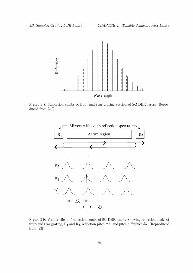
Reflection spectra of sampled gratings have comb-like structure, as in Figure 3-7. It will
be shown in subsequent sections that these comb separations depend on sampling period
of sampled grating. By implementing slightly different sampling period in front and rear
grating section, different reflection peak separation can be achieved. (Figure 3-8) The
relative position of these reflection combs can be altered by carrier injection (thus changing
the refractive index), and vernier-like effect can be apply to provide wide tuning range.
(Figure 3-9) This is to be discuss further in Section 3.3.2.
SG-DBR lasers (and also DBR, SSG-DBR, and GCSR) can be monolithically manufac-
tured thus enable integration with other key components [30], e.g. EA (Electro-absorbtion)
modulator [31, 32, 33], arrayed waveguide grating (AWG) [34], and wavelength monitor
[35, 36].
26

3.3. Sampled Grating DBR Lasers CHAPTER 3. Tunable Semiconductor Lasers
z
z
z
Real space Spatial frequency
uniform grating
modulation function
sampled grating
Bragg frequency
sampling period
grating length
grating pitch
Figure 3-6: Sampled grating and its spatial frequencies. [25]
3.3.1 Reflection properties of sampled grating
The discussion here followed those in [25] with slightly different notation. Sampled grating
is nothing more than uniform grating which is interrupted in periodic manner. The sampled
grating function can be written as product of uniform grating function and periodic modu-
lation function. The reflectivity of this structure can be then obtained from coupled-mode
equations. One prediction from coupled-mode theory is that every spatial Fourier compo-
nent of the refractive index perturbation give rise to a peak in reflection spectrum. [37]
Fourier transform of sampled grating can be obtained by convolving fourier transform of
uniform grating and the modulation function. As shown in Figure 3-6, this results in a
comb of fourier components centered at Bragg component of the uniform grating.
Figure 3-6 shows sampled grating structure with grating of pitch Λ and length Lg, with
sampling period Ls. Fourier components of sampled grating can be written as
fn = f0Lg
Lssinc(nπLg/Ls)e
iπnLg/Ls (3.2)
27

3.3. Sampled Grating DBR Lasers CHAPTER 3. Tunable Semiconductor Lasers
where f0 is Bragg wavelength of the uniform grating.
Reflection strength at each fourier component increases with coupling strength κn, which
is proportional to the fourier component itself. Coupling coefficient of each fourier compo-
nent of sampled grating can be written as
κn = κ0Lg
Lssinc(nπLg/Ls)e
iπnLg/Ls (3.3)
where κ0 is coupling strength of uniform grating.
A uniform grating with coupling strength κ has reflectivity given by [38]
r(λ) = Σniκ∗
nsin(qnLsg)
qncos(qnLsg) − i∆βnsin(qnLsg)(3.4)
where
∆βn =2πµ(λ)
λ+
iα
2−
π
Λ−
πn
Ls
= detuing from the nth component
q2n = ∆β2
n − |κn|2
Lsg = length of sampled grating structure
µ(λ) = refractive index at wavelength λ
Putting Equation (3.3) into (3.4), reflectivity of sampled grating structure is obtained.
This result is shown schematically in Figure 3-7.
Following characteristics of reflectivity in Figure 3-7 can be deduced from Equation (3.3)
and (3.4):
Peak power reflectivity of the nth order can be written as
Rn = tanh2(|κn|Lsg) (3.5)
The spacing between reflection peaks is given by
P =λ2
2µgLs(3.6)
28

3.3. Sampled Grating DBR Lasers CHAPTER 3. Tunable Semiconductor Lasers
Wavelength0
0.2
0.4
0.6
0.8
1
Ref
lect
ivity
Figure 3-7: Reflectivity of sampled grating structure
where µg is the group index.
Bandwidth of the nth peak is given by [25]
∆λn,bw =λ2
πµg
√
|κn|2 + (π/Lsg)2 (3.7)
It is shown that reflection peak separation is a function of sampling period Ls, thus
by employing slightly different Ls in front and rear grating and overlapping combs can be
obtained, as shown schematically in Figure 3-8
3.3.2 Vernier effect
As shown in Figure 3-8, reflection curves of grating sections of SG-DBR lasers have comb-
like characteristics, with slightly different pitches. This can be used to extend the tuning
range of the laser, as illustrated in Figure 3-9. By shifting position of one comb by δλ, the
pitch difference, the wavelength of incidence shifts by ∆λ, the pitch of the other reflection
comb. This means the tuning efficiency is enhanced by a factor of ∆λ/δλ from the limit
imposed by Equation 3.1.
This tuning by Vernier-like effect also means that wavelength will jump in step during
tuning. However, by shifting both reflection combs simultaneously, access can be gained to
29
3.3. Sampled Grating DBR Lasers CHAPTER 3. Tunable Semiconductor Lasers
Wavelength
Ref
lect
ion
Figure 3-8: Reflection combs of front and rear grating section of SG-DBR lasers (Repro-duced from [22])
Active regionR1 R2
R2
R1
R1'
Mirrors with comb reflection spectra
Figure 3-9: Vernier effect of reflection combs of SG-DBR lasers. Showing reflection peaks offront and rear grating, R1 and R2, reflection pitch ∆λ, and pitch difference δλ. (Reproducedfrom [22])
30

3.3. Sampled Grating DBR Lasers CHAPTER 3. Tunable Semiconductor Lasers
0 20 40 60 80 100Front curremt, mA
0
20
40
60
80
100
Rea
rcur
rent
,mA
1530 nm
1585 nm
Figure 3-10: Example of wavelength map of SG-DBR laser
every wavelength within the range, although not in a continuous way. (See for example,
Figure 3-10)
Shifting of reflection combs as described above can be achieved by injecting carrier into
grating sections, as was described in Section 3.1
3.3.3 Wavelength tuning characteristics
Figure 3-10 shows example of static wavelength tuning map of SG-DBR lasers, note the
fan-like mode characteristics. Each fan is dubbed supermode while the longitudinal modes
within each fan is called just a mode. Another characteristic worth notice is that tuning is
not continuous, as shown in Figure 3-11.
One major obstacle preventing wide spread use of tunable lasers at present time came
31

3.3. Sampled Grating DBR Lasers CHAPTER 3. Tunable Semiconductor Lasers
0 20 40 60 80 100Rear current, mA
1540
1550
1560
1570
1580
Wav
elen
gth,
nm
Figure 3-11: Section of wavelength map at front current = 30 mA
from the fact that each and every single laser fabricated has different tuning characteristics,
and thus needed to be characterized individually. The reason for this is the slight variation
across each laser chip during manufacturing process. These variation, although very small,
can cause noticeable effects on wavelength tuning characteristics.
This problem causes two main problem in implementation of tunable lasers. First, the
characterization process can took a long time. This problem has become less significant
as the technology matured, and characterization time was reduced from days of even week
down to a few hours. A new startup company, Intune Technologies [39], had focussed on
improving this characterizations process and claims it could take only about 10 minutes in
the future.
Another problem is the control system. With different tuning characteristics, each laser
has to be incorporated with its own wavelength lookup table. It is impractical to have high
resolution lookup table for each lasers, as the lookup process could be too slow, and with
effects of aging the table could not maintain accurate correspondence to the laser.
32

3.4. Wavelength Stabilization CHAPTER 3. Tunable Semiconductor Lasers
3.4 Wavelength Stabilization
This section discuss shortly the issue of wavelength stabilization, referencing, and monitor-
ing of tunable lasers. Whether tunable lasers are to be used as light sources or as part of
switching fabric, one very important problem that has to be address is wavelength stabi-
lization. Like other semiconductor devices, tunable lasers degrade over time and need to
be monitor to ensure perfect functionality over its life time. The effects of aging in tunable
semiconductors is, however, not yet fully understood and companies are doing life tests to
see how much and in which way these lasers degrade with time.
For WDM applications, the most important characteristics of laser aging is the wave-
length shift over time. It is required that the wavelength shift be much smaller than the
channel spacing of the system to avoid crosstalk. Other aspects of aging such as increased
threshold current are more tolerable.
Life time requirement for light source in telecommunication system is about 25 years,
and during that time conventional DFB lasers have wavelength drift of up to 0.25 nm. [40]
Tunable lasers have much more sophisticated spectral properties and to quantify the effects
of aging on wavelength shift is not clear cut.
One method to maintain wavelength precision during lasers life time is to lock the
wavelength to some kind of filter. Tunable lasers can operate on any wavelengths within
its tuning range, but telecommunication standards give the set of wavelength to be used as
evenly spaced grid in frequency. It is thus possible to use ethalon filter with suitable cavity
length to provide comb-like transmission spectra coincide with the frequency grid.
Analysis was given in [26] on wavelength stabilization of SSG-DBR laser. (As described
above, SG-DBR can be considered special case of SSG-DBR)
A practical implementation of such filter would be to detect small amount of light from
the laser with two detector, one with filter fitted in front. This way the variation of power
due to wavelength drift can be identify from power variation of the laser itself, which could
occur from aging.
33

Chapter 4
Wavelength Tuning Dynamics
Measurements had been done on dynamic tuning characteristics of SG-DBR lasers, using
bare laser chip the wavelength switching time was shown to be a few nanosecond. [41] In
this project, wavelength switchings were performed on laser modules supplied by Marconi
Caswell, and switchings were delayed by parasitic elements of laser modules. The results
presented here are thus not comparable to results performed on bare laser chip and do not
indicate the switching speed limit of these lasers, but conveyed information on switching
time of readily available tunable laser modules.
Definition of parameters
Before presenting any results on switching time measurement, it is necessary to make clear
the definition of many parameters used. In this report wavelength switching times are
identified and recorded in four numbers, rise time, fall time, and delay corresponded to rise
and fall transition. Rise and fall time are defined to be the time taken for power of the
particular wavelength to rise from 10% to 90% of the upper state power level, and vice
versa. Rise and fall delay are times taken for the switching process to begin, measured from
trigger point on driving signal. (Figure 4-1)
These parameters were chosen because they offered easy and definitive mean of com-
paring switching speed. Digital oscilloscope used in the experiment (by LeCroy) offered
automatic measurements of rise and fall time, while delay were manually measured.
34

CHAPTER 4. Wavelength Tuning Dynamics
mean
90%
10%
rise time fall time
upper state
lower state
rise delay fall delay
Figure 4-1: Definition of rise time, fall time, and delays. Driving current signal (above) andpower varation of one wavelength (lower) are shown. Not to scale.
35

4.1. Experimental Setup CHAPTER 4. Wavelength Tuning Dynamics
Function Generator
Current sources
Tunable laser Tunable bandpass filter
Photo Detector
Digital Oscilloscope trigger signal
Temperature controller
Figure 4-2: Diagram of the experimental set up
4.1 Experimental Setup
Figure 4-2 shows how switching time measurements were done. Three out of four currents
(gain, front grating, and phase) required to drive SG-DBR laser were provide by current
sources, while rear grating current was generated by a function generator providing square
wave. Laser output was then passed onto tunable bandpass filter, which allow only one
wavelength component to pass through. Optical signals were then detected by a photode-
tector and analyse on the digital oscilloscope. Laser’s temperature was controlled at all
time by feedback loop and thermoelectric coupler, to maintain temperature at 25 degree
celsius.
Detailed information on components used in the experiment is presented in Table 4.1
4.2 Results
Using configuration described in previous section, only one wavelength can be analysed at
a time. However, by storing the output waveform of each wavelength then display them
together, the nature of wavelength switching dynamic can be study, as shown for example
36

4.2. Results CHAPTER 4. Wavelength Tuning Dynamics
Components Make / Model Calibration status Remarks
Function Generator HP 8116A In calibration Rise/Fall time 10 ns
Output impedance 50Ω
Digital Oscilloscope LeCroy Waverunner In Calibration Bandwidth 500 MHz
LT344 Input impedance 50Ω / 1MΩ
Tunable Bandpass Dicon Fiberoptics Not subject to Tuning range 1,535-1,565 nm
Filter TF-1565-0.8-FC-3.0-1 calibration 0.5-dB bandwidth 0.8 nm
Temperature Controller ILX Lightwave LDT-5142 In calibration
Power Supply X 3 Thurlby 30V-1A Not subject to Output impedance < 5mΩ
calibration
Digital Multimeter Kiethley 177 / 179A In calibration Resolution 0.01 mA
Thurlby 1503-HA 3 months out of Resolution 0.1 mA
calibration
Table 4.1: Equipments used
in Figure 4-3. Note that dynamics of both wavelengths are identical, except for a scaling
factor in power.
All semiconductor lasers being investigated here are four-sections SG-DBR lasers, with
different active region geometry, these will be called laser I and laser II. Laser I is one of
the early manufactured module and has buried ridge structure, while relatively new laser II
has has surface ridge structure. Surface ridge structure offered higher output power but is
subject to poorer thermal properties.
4.2.1 Switching Time
Switchings were done between two wavelengths, by changing current in rear grating section
in periodic manner. Output power scanning shows that stable operating points usually lie
in the middle of each modes, thus care had been taken to ensure that switchings occur
between these stable regions. Wavelength pairs studied in laser I are shown in Figure 4-4.
Preliminary results suggested that delay times do not varied significantly among wave-
lengths pair, thus interests had been focused on investigating rise and fall time of each
wavelength components. Figure 4-5 shows switching time for both kind of lasers at various
wavelength separations. Each of these results is averaged over more than 500 oscilloscope’s
sweeps at the particular wavelength pair. Wavelength separations used were restricted by
the filter bandwidth (∼ 1 nm), and reflection peak separation of sampled grating (∼ 6-7
37

4.2. Results CHAPTER 4. Wavelength Tuning Dynamics
0 10 20 30 40 50 60 70 80 90 100Time, microsecond
Opt
ical
Pow
er
0 10 20 30 40 50 60 70 80 90 100
Figure 4-3: Wavelength switching between 1540.3 and 1552.7 nm in buried ridge laser
nm) as only one current was varied.
In both lasers, switching times differ greatly between rise and fall transition of each
wavelength. These fall times do not differ significantly between two lasers, but rise times
are shorter in laser II by an order of magnitude. This difference in switching time is due to
different packaging and bonding within laser modules, and not to the different gain section
geometry. This can be confirmed as switching time measured on bare buried ridge structure
laser chip was shown to be only a few nanoseconds. [41, 42, 43]
Results presented for laser I might suggested that switching time increase with wave-
length separation, as observed in measurements on bare laser chips. Subsequent mea-
surements, however, show that switching times do not notably increase when wavelength
separation was increase up to about 20 nm. This is observed in both lasers. These results
can be explained as followed: as variation of switching time versus wavelength separation
occurs on nanosecond timescale, while in studied laser switching times are limit by parasitic
elements to about 1 µs in laser I and 100 ns in laser II, the expected switching time variation
with wavelength separation was thus rendered unobservable.
Better module design can improve switching speed to near the limit imposed by laser
chips themself, as shown in results obtained from GCSR lasers manufactured by Altitun AB,
with switching time about 30 ns. [44]. (Enhanced to about 5 ns with pulse pre-distortion
38

4.2. Results CHAPTER 4. Wavelength Tuning Dynamics
0 5 10 15 20 25Front curremt, mA
0
5
10
15
20
25
Rea
rcur
rent
,mA
0 5 10 15 20 25
0
5
10
15
20
25
1490 nm
1560 nm
Figure 4-4: Wavelength map showing example of wavelength pairs being measured in buriedridge laser
39

4.2. Results CHAPTER 4. Wavelength Tuning Dynamics
6.1 6.15 6.2 6.25 6.3 6.35 6.4Wavelength separation, nm
0.8
1
1.2
1.4
1.6
1.8
Tim
e,m
icro
seco
nd
Backward
Forward
(a) Buried ridge, Rise time
6.1 6.15 6.2 6.25 6.3 6.35 6.4Wavelength separation, nm
6.8
6.9
7
7.1
7.2
7.3
Tim
e,m
icro
seco
nd
Backward
Forward
(b) Buried ridge, Fall time
6 6.25 6.5 6.75 7 7.25 7.5 7.75Wavelength separation, nm
70
80
90
100
110
Tim
e,ns
Backward
Forward
(c) Surface ridge, Rise time
6 6.25 6.5 6.75 7 7.25 7.5 7.75Wavelength separation, nm
7.8
8
8.2
8.4
8.6
8.8
9T
ime,
mic
rose
cond
Backward
Forward
(d) Surface ridge, Fall time
Figure 4-5: Measured switching time of (a),(b)buried ridge laser and (c),(d)surface ridgelaser, versus wavelength separation
technique, to be discussed in section 4.3)
4.2.2 Intermediate Mode Suppression Ratio
When switching involved more than one mode hop, intermediate modes are excited. This
contributes to crosstalk and thus it is interesting to see what the mode suppression ration
is. Both types of lasers had been investigate and the results are that there is no significant
difference on mode suppression ratio. (See Figure 4-6) Power ratio between the higher of
start/stop mode and the unwanted intermediate mode is 28.9 dB and 29.8 dB for buried
ridge and surface ridge laser, respectively. Note that this is for particular pair of wavelength
40

4.2. Results CHAPTER 4. Wavelength Tuning Dynamics
1535 1540 1545 1550 1555 1560 1565 Wavelength , nm
- 50
- 40
- 30
- 20
- 10
0
Opt
ical
Pow
er , d
Bm
(a) Buried ridge structure
1535 1540 1545 1550 1555 1560 1565 Wavelength , nm
- 40
- 30
- 20
- 10
0
10
Opt
ical
Pow
er , d
Bm
(b) Surface ridge structure
Figure 4-6: Mode suppression ratio during wavelength switching
and the switching current rise time is about 7 ns.
4.2.3 Effect of electronics impedance
It was shown that parasitic elements and electrical bonding within laser modules have great
effect on switching time. It is also equally important to match impedance of driving circuit
and the device itself to optimize electrical connection and thus switching speed. To choose
the best value of series resistance to use, measurements were done on the the dependency
of switching time on series resistance, and results are shown in Figure 4-7.
These measurements were done on a SG-DBR laser module, by switching laser’s wave-
length between 1538.4 nm and 1544.5 nm at the rate of 20 kHz, up-conversion means
transition from shorter wavelength to the longer, and vice versa for down-conversion. Driv-
ing current are in the form of square wave, with amplitude and DC offset adjusted to give
roughly the same current step when used with different series resistor.
Tradeoff between forward and backward switching time can be obviously seen and value
of series resistance about 50 Ω gives reasonable compromising.
41

4.3. Pulse Pre-distortion technique CHAPTER 4. Wavelength Tuning Dynamics
40 60 80 100Wavelength separation, nm
1.1
1.2
1.3
1.4
1.5
1.6
Tim
e,m
icro
seco
nd
Backward
Forward
(a) Rise time
40 60 80 100Wavelength separation, nm
6.8
6.9
7
7.1
7.2
7.3
Tim
e,m
icro
seco
nd
Backward
Forward
(b) Fall time
Figure 4-7: Measured switching time of buried ridge laser versus series resistance
4.3 Pulse Pre-distortion technique
In most type of tunable semiconductor lasers, including SG-DBR lasers, the ultimate lower
limit of switching time is impose by carrier lifetime in active region. This is an intrinsic
property of the material and cannot be easily changed.
However, carrier dynamics in active region, and thus switching characteristics, can be
manipulate by changing the way lasers are driven. It is known that switching time can
be reduced by employing pulse pre-distortion technique. [45, 12] This was originally done
using two laser drivers and differentiator (Figure 4-8), but this is difficult to use with
multi-wavelength switching as different differentiator characteristics will be required for
each wavelength pairs. Fukashiro et al. [44] suggested driver unit based on digital-to-analog
converters (DACs) with current sources to produce pre-distorted current pulse. This provide
configurable driver capable of fast-switching between any desired wavelengths.
The pulse pre-distortion technique discussed above has only been demonstrated on
GCSR type lasers by switching current applied to coupler [45] or reflector [12, 44] section,
but should apply generally to carrier injection tuning of any semiconductor lasers.
Pulse pre-distortion technique had been implemented with both lasers studied, and by
varying the overshoot size and duration some better performance had been observed. This
enhancement of switching time is, however, not as significant as in other works [45,44], and
42

4.4. Thermal drift CHAPTER 4. Wavelength Tuning Dynamics
Current Driver Current Driver
Driving current
Figure 4-8: Pulse pre-distortion based on differentiator
the origin of this finding will be discussed.
Driving used in this experiment has rise/fall time of about 10 ns, which is on the
same order as switching times reported. [41, 42, 44] It is thus clear that faster driver is
needed to obtain better performance. The driving circuit also already exhibit overshoot
characteristics, which could be from capacitance in the circuit. This internal overshoot has
duration of about 0.5 µs. This explained why switching time enhancement was not observed
when pulse pre-distortion technique was implemented with laser II, as 0.5 µs is much longer
than the laser’s rise time. (about 0.1 µs) All these indicated that with better driving unit,
shorter switching time should be achievable.
Another benefit offered by pulse pre-distortion technique is reduced Mode Suppression
Ratio during wavelength switching. [44] This phenomena was observed and result was shown
in Figure 4-9. Mode suppression ratio was increase by about 3.5 dB.
4.4 Thermal drift
So far, only electronic effects had been considered, this is because the time scale imposed
by packet-switched networks are much smaller than that of thermal effects of lasers. How-
ever, it has to be noted that switching performed in this project only occurs between two
wavelengths and thermal equilibrium had been reached. In real world, traffics come with
various characteristics, e.g. gaussian, random inhomogeneous traffic, or bursty traffic, and
43

4.4. Thermal drift CHAPTER 4. Wavelength Tuning Dynamics
1535 1540 1545 1550 1555 1560 1565 Wavelength , nm
- 50
- 40
- 30
- 20
- 10
0
Opt
ical
Pow
er , d
Bm
(a) Without pre-distorted pulse
1535 1540 1545 1550 1555 1560 1565 Wavelength , nm
- 50
- 40
- 30
- 20
- 10
0
Opt
ical
Pow
er , d
Bm
(b) With pre-distorted pulse
Figure 4-9: Intermediate Mode suppression enhancement with pulse pre-distortion tech-nique
these will have different effects on longer-timescale thermal properties of tunable lasers, and
thus their tuning characteristics. Cares had to be taken in the control of these lasers, to
ensure correct functionality over time and changing traffic.
44

Chapter 5
Conclusion
Comparing the switching speeds measured and the requirement for packet switching, it can
be seen that the modules tested do not offer the desired performance. However, the ultimate
limit of switching speed had net yet been reached, and wavelength routing with tunable
transmitters had great potential in eventually deliver switching on packet-by-packet basis.
Many switch and network configurations had been proposed to date, and demonstrations
on small scale networks show promising results.
45

Appendix A
Arrayed Waveguide Grating
devices
This appendix on arrayed waveguide grating followed closely those treatment in [2]. The-
oretical results are presented for inderstanding of how the device perform when used as
wavelength router. Readers are refered to reference given in Chapter 8 of [2] for more
detailed discussion on applications and performance of AWG devices.
Star coupler couples light from any input to all output port and, ideally, split the power
evenly. The device consist of array of input and output waveguide (fiber) connected by a
waveguide slab. (Figure A-1)
Figure A-1: Star coupler
And Figure A-2 shows, AWG form by two star couplers connected by number of waveg-
uides. If these waveguides has identical length, AWG would just direct signal from nth
input port to the nth output port. However, if these waveguides has linearly increasing
46

CHAPTER A. Arrayed Waveguide Grating devices
length, the waveguides can act as grating by distorting the wavefront emerge from them.
The waveguide itself exhibit certain dispersion, thus the path different experienced by dif-
ferent wavelengths are not the same, and the amount that wavefronts are distorted therefore
varied.
Figure A-2: Arrayed waveguide grating
With suitable design, AWG can perform as a wavelength router by directing signal from
input to output port according to wavelength and input port number. AWG can be of
miniature dimensions and integration with semiconductor lasers had been demonstrated.
The maximum number of port to date is to device produced at NTT, Japan, with 256 input
and output ports, and 25 GHz channel spacing. [10]
Another interesting property of AWG router is that wavelength are wrapped around,
i.e. wavelength λi and λi + ∆λFSR will be route to the same output port, where ∆λFSR is
the free spectral range of the device and is equal
∆λFSR =λ2
ngl(A.1)
where ng is the group index and l is the path length different in the waveguides.
47

Bibliography
[1] S. M. Gemelos, I. M. White, D. Wonglumson, K. Shrikhande, T. Ono, and L. G.Kazovsky, “WDM metropolitan area network based on CSMA/CA packet swithching,”IEEE Photonics Technol. Lett., vol. 11, pp. 1512–1514, November 1999.
[2] I. P. Kaminow and T. L. Koch, eds., Optical fiber Telecommunications, vol. IIIB. Aca-demic Press, 1997.
[3] C. Guillemot, M. Renaud, P. Gambini, C. Janz, I. Andonovic, R. Bauknecht,B. Bostica, M. Burzio, F. Callegati, M. Casoni, D. Chiaroni, F. Clerot, S. L.Danielsen, F. Dorgeuille, A. Dupas, A. Franzen, P. B. Hansen, D. K. Hunter, A. Kloch,R. Krahenbuhl, B. Lavigne, A. LeCorre, C. Raffaelli, M. Schilling, J.-C. Simon, andL. Zucchelli, “Optical packet switching: The european ACTS KEOPS project ap-proach,” J. Lightwave Technol., vol. 16, pp. 2117–2134, December 1998.
[4] G. Bendelli, M. Burzio, P. Gambini, and M. Puleo, “Performance assessment of aphotonic ATM switch based on a wavelength-controlled fiber loop buffer,” in Proceedingon Conference on Optical Fibers and Communications, pp. 106–107, 1996.
[5] D. J. Blumenthal, R. J. Feuerstein, and J. R. Sauer, “First demonstration of multihopall-optical packet switching,” IEEE Photon. Technol. Lett., vol. 6, pp. 457–460, March1993.
[6] F. forghieri, A. Bononi, and P. R. Prucnal, “Analysis and comparison of hot-potatoand single-buffer deflection routing in very high bit rate optical mesh networks,” IEEETrans. Commun., vol. 43, pp. 88–98, January 1995.
[7] D. K. Hunter, M. C. Chia, and I. Andonovic, “Buffering in optical packet switches,”J. Lightwave Technol., vol. 16, pp. 2081–2094, December 1998.
[8] P. Heywood, “Xros launches first 1000-port all optical cross connect.” March 2000.
[9] “Spectra switch optical products wave walker n-1x2.” www.spectraswitch.com, 2000.
[10] Y. Hida, Y. Hibino, M. Itoh, A. Sugita, A. Himeno, and Y. Ohmori, “Fabricationof low-loss and polarisation-insensitive 256 channel arrayed-waveguide grating with 25ghz spacing using 1.5% δ waveguides,” Electron. Lett., vol. 36, pp. 820–821, April 2000.
[11] K. Sasayama, Y. Yamada, Habara, and K. Yukimatsu, “FRONTIERNET: Frequency-routing-type time-division interconnection network,” IEEE J. Lightwave Technol.,vol. 15, pp. 485–488, March 1997.
48

BIBLIOGRAPHY BIBLIOGRAPHY
[12] A. Carena, M. D. Vaughn, R. Gaudino, M. Shell, and D. J. Blumenthal, “OPERA:An optical packet experimental routing architecture with label swapping capability,”J. Lightwave Technol., vol. 16, pp. 2135–2145, December 1998.
[13] W. D. Zhong and R. S. Tucker, “A wavelength-routing based photonic packet buffer andits application in photonic packet switching system,” J. Lightwave Technol., vol. 16,pp. 1737–1745, October 1998.
[14] B. Glance and M. J. Karol, “Large capacity multi-access wavelength division multi-plexing packet network.” United States Patent number 5,455,699, October 1995.
[15] N. Yamanaka, K. Shimoto, E. Oki, and S. Yasukawa, “ATM switch.” United StatesPatent number 5,892,604, April 1999.
[16] T. Ono, S. Gemelos, I. White, and L. g. Kazovsky, “Latency characteristics ofwavelength-switched packets in wdm multi-hop ring network,” in Proceeding on Con-ference on Optical Fibers and Communications, no. ThM8-1, (San Diego), pp. 183–185,1999.
[17] D. Wonglumson, I. M. White, S. M. Gemelos, K. Shrikhande, and L. G. Kazovsky,“HORNET–a packet-switched WDM network: Optica packet transmission and recov-ery,” IEEE Photonics Technol. Lett., vol. 11, pp. 1692–1694, December 1999.
[18] I. M. White, Y. Fukashiro, K. Shrikhande, D. Wonglumson, M. S. rogge, M. Avenar-ius, and L. G. Kazovsky, “Experimental demonstration of a media access protocol forHORNET: A WDM multiple access metropolitan area ring network,” in Proceeding onConference on Optical Fibers and Communications, no. WD3-1, (Baltimore), March2000.
[19] I. M. White, Y. Fukashiro, K. Shrikhande, D. Wonglumson, M. Rogge, M. Avenarius,and L. Kazovsky, “Experimental demonstration of a media access scheme for HORNET:A WDM multiple-access metropolitan area ring network,” in Proceeding on Conferenceon Optical Fibers and Communications, 2000.
[20] K. Kato, A. Okada, Y. Sakai, K. Noguchi, T. Sakamoto, S. Suzuki, A. Takahara,S. Kamei, A. Kaneko, and M. Matsuoka, “32 X 32 full-mech (1024 path) wavelength-routing WDM network based on uniform-loss cyclic-frequency arrayed-waveguide grat-ing,” Electron. Lett., vol. 36, July 2000.
[21] M. Shell, M. D. Vaughn, A. Wang, D. J. Blumenthal, P.-J. Rigole, and S. Nilsson,“Experimental demonstration of an all-optical routing node for multihoip wavelengthrouted networks,” Photonics Technology Letters, vol. 8, pp. 1391–1393, October 1996.
[22] M.-C. Amann and J. Buus, Tunable Laser Diodes. Artech House, 1998.
[23] T. Koch, U. Koren, R. Gnall, C. Burrus, and B. Miller, “Continuously tunable 1.5 µmmultiple-quantum well GaInAs/GaInAsP distributed-bragg-reflector lasers,” Electron.Lett., vol. 24, pp. 1431–1433, November 1998.
49

BIBLIOGRAPHY BIBLIOGRAPHY
[24] L. A. Coldren, “Multi-section tunable laser with differing multi-element mirrors.”United State Patent number 4,896,325, January 1990.
[25] V. Jayaraman, Z.-M. Chuang, and L. A. Coldren, “Theory, design, and performance ofextended tuning range semiconductor lasers with sampled gratings,” IEEE J. QuantumElectron., vol. 29, pp. 1824–1834, June 1993.
[26] H. Ishii, F. Kano, Y. Tohmori, Y. Kondo, T. Tamamura, and Y. Yoshikuni, “Nar-row spectral linewidth under wavelength tuning in thermally tunable super-structure-grating (SSG) DBR lasers.,” IEEE J. Sel. Top. Quantum Electron., vol. 1, pp. 401–407,1995.
[27] J. Willems, G. Morthier, and R. Baets, “Novel widely tunable integrated optical filterwith high spectral selectivity,” in 18th European Conference on Optical Communication(ECOC’92), (Berlin, Germany), pp. 413–416, 1992.
[28] B. Broberg, P.-J. Rigole, S. Nilsson, L. Andersson, and M. Renlund, “Widely tunablesemiconductor lasers,” in Proceeding on Conference on Optical Fibers and Communi-cations, no. WH4-1, (San Diego), pp. 137–139, 1999.
[29] P. Heywood, “Tune In!.” www.lightreading.com, April 2000.
[30] S.-L. Lee, I.-F. Jang, C.-Y. Wang, C.-T. Pien, and T.-T. Shih, “Monolithically inte-grated multiwavelength sampled grating DBR lasers for dense WDM applications,”IEEE Journal of Selected Topics in Quantum Electronics, vol. 6, pp. 197–206, Jan-uary/February 2000.
[31] B. Mason, G. A. Fish, S. P. DenBaars, and L. A. Coldren, “Widely tunable sampledgrating dbr laser with integrated electroabsorption modulator,” Photon. Tech. Letts.,vol. 11, pp. 638–640, June 1999.
[32] B. Mason, G. A. Fish, S. P. DenBaars, and L. A. Coldren, “Monolithic integration ofa widely tunable laser and an electroabsorption modulator,” in Integrated PhotonicsResearch ’99, no. RME2, (Santa Barbara, CA), pp. 53–55, July 1999.
[33] B.-S. Kim, Y. Chung, and S.-H. Kim, “Dynamic analysis of widely tunable laser diodesintegrated with sampled- and chirped-grating distributed bragg reflectors and elec-troabsorption modulator,” IEICE Trans. Electron., vol. E81-C, pp. 1342–1349, August1998.
[34] S. Menezo, A. R. andA. Talneau, F. Delorme, S. Grosmaire, H. Nakajima, E. Vergnol,F. Alexandre, and F. Gaborit, “Design, realization, and characterisation of a ten-wavelength monolithic source for wdm applications integrating dbr lasers with aphasar,” IEEE J. Sel. Top. Quantum Electron., vol. 6, pp. 185–190, January/February2000.
[35] B. Mason, O. A. Lavrova, G. A. Fish, S. P. Denbaars, and L. A. Coldren, “Sampledgrating DBR lasers with integrated wavelength monitoring,” in Integrated PhotonicsResearch ’98, no. IMD5, (Victoria, Canada), pp. 52–54, March 1998.
50

BIBLIOGRAPHY BIBLIOGRAPHY
[36] B. Mason, S. P. DenBaars, and L. A. Coldren, “Tunable sampled grating DBR laserswith integrated wavelength monitors,” IEEE Photon. Techn.Letts., vol. 10, pp. 1085–1087, August 1998.
[37] A. Yariv and P. Yeh, Optical Waves in Crystal. New York: Wiley, 1984.
[38] G. P. Agrawal and N. K. Dutta, Long Wavelength Semiconductor Lasers. New York:Van Nostrand Reinhold, 1986.
[39] “Intune technologies.” www.intune-technologies.com.
[40] Y. C. Chung, J. Jeong, and L. S. Cheng, “Aging-induced wavelength shifts in 1.5-µmDFB lasers,” IEEE Photonics Technol. Lett., vol. 6, pp. 792–795, July 1994.
[41] R. O’Dowd, “Tunable and agile laser transmitter developments for future DWDM opti-cal networks: Towards managed wavelength control and switching,” Photonic NetworkCommunications, vol. 2, no. 1, pp. 97–103, 2000.
[42] T. Mullane, T. Farrell, J. Dunne, Y. Yu, and R. O’Dowd, “Ultra-fast measurementsof a sg-dbr laser with picosecond time and nanometre wavelengthresolution using afabry-perot interferometer.,” in IEEE Lasers and Electro-Optics Conference ’99, (San-francisco), November 1999.
[43] M. Kuznetsov, J. Stone, and L. W. Stulz, “Time- and frequency-resolved measurementsof frequency modulation and switching of a tunable semiconductor laser,” Appl. Phys.Lett., vol. 59, pp. 2492–2494, November 1991.
[44] Y. Fukashiro, K. Shrikhande, M. Avenarius, M. Rogge, I. M. White, D. Wonglumson,and L. G. Kazovsky, “Fast and fine wavelength tuning of a GCSR laser using a digitallycontrolled driver,” in Proceeding on Conference on Optical Fibers and Communications,no. WM43, (Baltimore, MD), March 2000.
[45] P. J. Rigole, M. Shell, S. Nilsson, D. J. Blumenthal, and E. Berglind, “Fast wavelengthswitching in a widely tunable GCSR laser using a pulse pre-distortion technique,” inProceeding on Conference on Optical Fibers and Communications, no. WL63, (Dallas),pp. 231–232, February 1997.
51
![Stewart, Amy (DBR) · From: Bannister, Jorge (DBR) To: Stewart, Amy (DBR) Cc: Taylor, Tina (DBR); Desilets, LeeAnn (DBR) Subject: FW: [EXTERNAL] : Food Trucks Date: Friday, February](https://static.fdocuments.in/doc/165x107/5fb3a34c68602c67914aec27/stewart-amy-dbr-from-bannister-jorge-dbr-to-stewart-amy-dbr-cc-taylor.jpg)