Camera-Based Calibration Techniques for Seamless Multi-Projector ...
On Calibration Techniques for Pipelined ADCs
Swina Narula, and Sujata Pandey* Amity School of Engineering & Technology, Amity University, Noida
*Amity Institute of Telecom Engineering and Technology, Amity University Noida, INDIA Email: [email protected]
Abstract: The development and designing of advanced pipelined analog to digital converter (ADC) is becoming sophisticated day by day as dimensions and supply voltages used for devices are reducing. As the nanometer technology aids fabricating circuits with small footprints, we require high-performance Pipelined ADCs, which are able to rectify analog circuit non-idealities with digital calibration circuits. Digital background calibration is the most favorable solution instead of making changes in analog components in the deep submicron processes. This paper discusses some of the techniques for digital calibration that have been accepted to realize advanced pipelined ADCs. It was observed that on an average, for every two years, the efficiency of ADCs is enhanced by a factor of two. With constant technology scaling supply voltages have reduced and the devices operate at high speed. A closer inspection on SNDR, SFDR, INL and DNL of pipelined ADCs with different calibration techniques is presented here. Finally, a comparison on various design approaches is made to make a view towards additional enhancement in speed, power efficiency and functioning of ADCs.
Key words: pipelined ADCs, calibration techniques, SNDR, SFDR, INL, DNL
I. INTRODUCTION
There are variety ofapplications of pipelined ADCs like broadband communication transceivers, video imaging systems, cable head ends i.e. for digitizing cable modem uplinks, medical instrumentation, professional HDTV cameras, cellular base station and military. The Pipelined ADC having multistage architecture deals with a solution for low power, high resolution, high speed and chip area. Applications based on low resolution requirement like 8-10 bit resolution may use various power reduction techniques [1-3]. It’s really hard to achieve the speed of the ADCs exceeding 100 MS/s with resolution beyond 12-bit without applying any calibration technique. As the resolution of ADC increases, the hardware complexity also increases. Due to switched capacitor circuits used in MDAC of pipelined ADC, various errors like op amp nonlinearity, capacitor sizing error andOP-AMP with finite gain may come in picture.
As CMOS technologies are scaling down, amplifiers with high gain are difficult to fabricate. Also capacitor sizing issues degrades the performance of ADCs. There are so many techniques available to minimize these errors [4-10]. All these techniques have their own advantage, disadvantages and limitations. A comparison of these techniques for digital calibration is not available in literature till now.
The purpose of this paper is to analyze and compare different digital calibration techniques with their advantages that have been developed and used in various applications. Some important calibration techniques like nested background calibration, calibration using least mean square method, SPLIT, variable amplitude dithering, equalization based calibration, inter-stage scaling, two way interleaved and interpolation based nonlinear calibration has been discussed in details. There are five sections in this paper. Section II outlines pipelined ADCs with different errors and Section III emphasizes on the motivation behind the subject and different categories of calibration techniques. Section IV discusses the available techniques for digital calibration used for pipelined ADCs and their comparative analysis.
II. PIPELINED ADC ARCHITECTURE AND DIFFERENT ERRORS
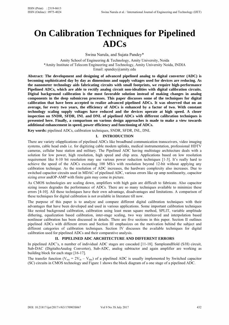
In pipelined ADC’s, n number of individual ADC stages are cascaded [11-18]. SampleandHold (S/H) circuit, Sub-DAC (DigitaltoAnalog Converter), Sub-ADC, analog subtractor and again amplifier are working as building block for each stage [16-17].
The transfer function (Vres = 2Vin – Vdac) of a pipelined ADC is usually implemented by Switched capacitor (SC) circuits in CMOS technology and Figure 1 shows the block diagram of a one stage of a pipelined ADC.
ISSN (Print) : 2319-8613 ISSN (Online) : 0975-4024 Swina Narula et al. / International Journal of Engineering and Technology (IJET)
DOI: 10.21817/ijet/2017/v9i3/170903S067 Vol 9 No 3S July 2017 432
Correcti
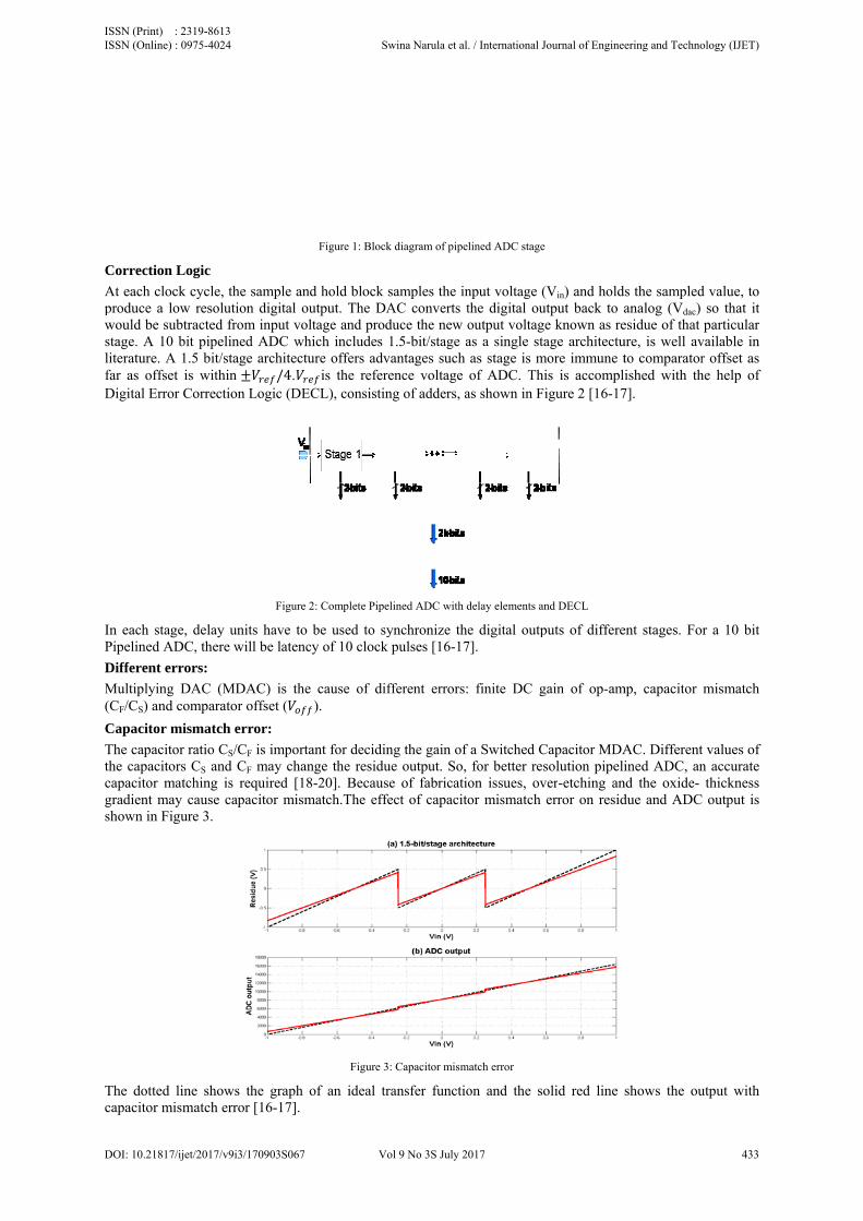
At each cproduce would bestage. A literaturefar as ofDigital E
In each sPipelined
Differen
Multiplyi(CF/CS) a
Capacito
The capathe capaccapacitorgradient shown in
The dottcapacitor
ion Logic
clock cycle, tha low resolut
e subtracted fr10 bit pipelin
e. A 1.5 bit/staffset is withinError Correctio
stage, delay ud ADC, there w
t errors:
ing DAC (Mand comparato
or mismatch
acitor ratio CS/citors CS and r matching is may cause ca
n Figure 3.
ed line showr mismatch err
he sample andtion digital ourom input volned ADC whiage architectun /4.on Logic (DEC
Figure 2
units have to will be latency
MDAC) is the or offset (
error:
/CF is importaCF may chanrequired [18
apacitor mism
ws the graph oror [16-17].
Figure 1: Block
d hold block sutput. The DAtage and prodich includes 1
ure offers advis the refere
CL), consistin
2: Complete Pipel
be used to syy of 10 clock
cause of dif).
ant for decidinnge the residu8-20]. Becausematch.The effe
Figure 3
of an ideal tr
k diagram of pipe
samples the inAC converts tduce the new o1.5-bit/stage a
vantages such ence voltage ng of adders, a
lined ADC with d
ynchronize thepulses [16-17
fferent errors:
ng the gain of ue output. So, e of fabricatioect of capacito
: Capacitor mism
ransfer functio
lined ADC stage
nput voltage (the digital ououtput voltageas a single staas stage is mof ADC. Thi
as shown in Fi
delay elements an
e digital outp7].
finite DC g
a Switched Cfor better res
on issues, ovor mismatch
match error
on and the so
Vin) and holdtput back to ae known as reage architectu
more immune tis is accompligure 2 [16-17
nd DECL
puts of differe
ain of op-am
Capacitor MDAsolution pipeliver-etching anerror on resid
olid red line
ds the sampledanalog (Vdac) esidue of that ure, is well avto comparatorished with th
7].
ent stages. Fo
mp, capacitor
AC. Differentined ADC, an
nd the oxide- due and ADC
shows the ou
d value, to so that it particular
vailable in r offset as he help of
r a 10 bit
mismatch
t values of n accurate thickness
C output is
utput with
ISSN (Print) : 2319-8613 ISSN (Online) : 0975-4024 Swina Narula et al. / International Journal of Engineering and Technology (IJET)
DOI: 10.21817/ijet/2017/v9i3/170903S067 Vol 9 No 3S July 2017 433
Compar
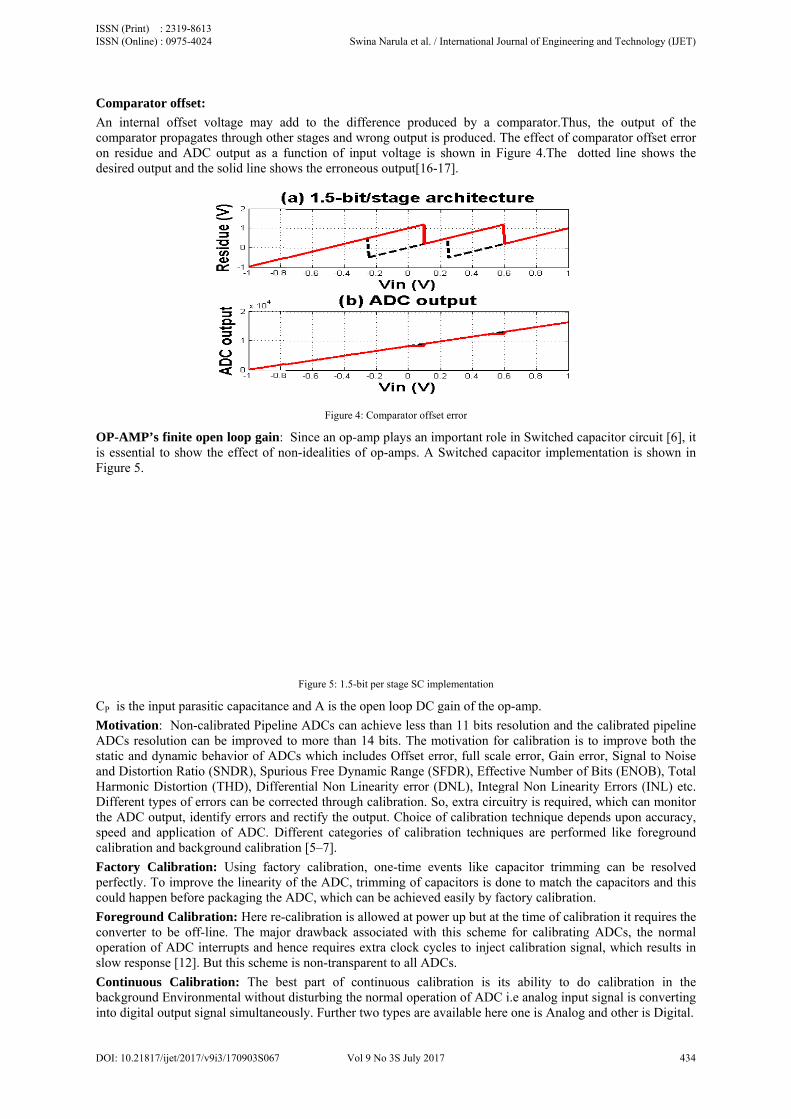
An intercomparaton residudesired o
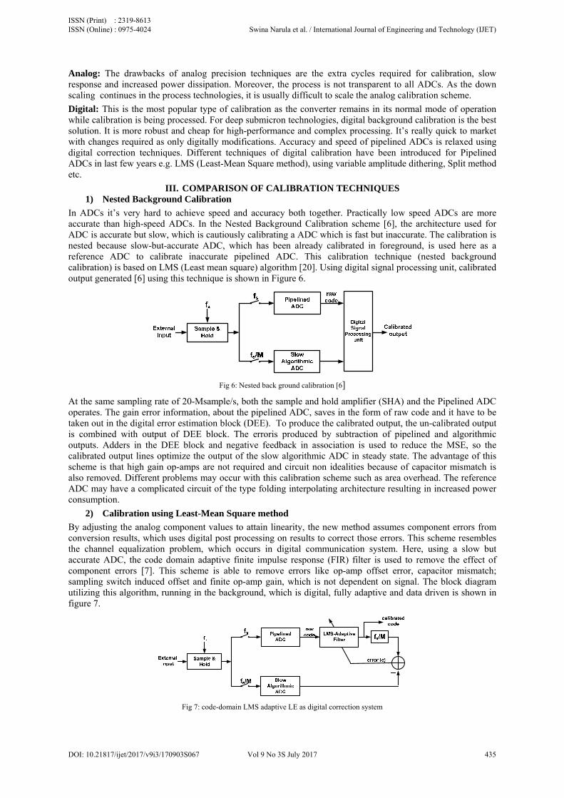
OP-AMPis essentiFigure 5.
CP is the
MotivatiADCs restatic andand DistoHarmoniDifferentthe ADCspeed ancalibratio
Factory perfectlycould hap
Foregrouconverteroperationslow resp
Continuobackgrouinto digit
rator offset:
rnal offset votor propagatesue and ADC output and the
P’s finite opeial to show th
e input parasiti
ion: Non-caliesolution can bd dynamic behortion Ratio (Sc Distortion (t types of erro
C output, identnd applicationon and backgr
Calibration:y. To improve ppen before p
und Calibratr to be off-linn of ADC inteponse [12]. Bu
ous Calibratund Environmtal output sign
oltage may as through otheoutput as a fsolid line sho
en loop gain: he effect of no
ic capacitance
ibrated Pipelinbe improved havior of ADSNDR), Spuri(THD), Differors can be corrtify errors and
n of ADC. Diround calibrati
: Using factothe linearity ackaging the A
tion: Here re-cne. The majoerrupts and heut this scheme
tion: The bemental without nal simultaneo
dd to the difer stages and wfunction of inows the errone
Figure 4
Since an op-aon-idealities o
Figure 5: 1.5-b
e and A is the
ne ADCs can to more than
DCs which incious Free Dynrential Non Lrected throughd rectify the oifferent categoion [5–7].
ory calibrationof the ADC, tADC, which c
calibration is r drawback aence requires e is non-transp
est part of codisturbing the
ously. Further
fference prodwrong output nput voltage ieous output[16
4: Comparator off
amp plays an of op-amps. A
bit per stage SC i
open loop DC
achieve less 14 bits. The
cludes Offset enamic Range (
Linearity errorh calibration.
output. Choiceories of calib
n, one-time etrimming of ccan be achieve
allowed at poassociated witextra clock c
parent to all A
ontinuous cae normal opertwo types are
duced by a cis produced. T
is shown in F6-17].
ffset error
important rolA Switched ca
implementation
C gain of the o
than 11 bits rmotivation foerror, full sca(SFDR), Effecr (DNL), IntegSo, extra circ
e of calibratiobration techniq
events like ccapacitors is ded easily by fa
wer up but at th this schemycles to injec
ADCs.
libration is iration of ADCe available her
comparator.ThThe effect of
Figure 4.The
e in Switchedapacitor imple
op-amp.
resolution andor calibration ale error, Gainctive Numbergral Non Linecuitry is requirn technique dques are perf
capacitor trimdone to match factory calibra
the time of cae for calibrat
ct calibration s
its ability to C i.e analog inpre one is Analo
hus, the outpcomparator o dotted line s
d capacitor circementation is
d the calibratedis to improve
n error, Signalr of Bits (ENOearity Errors (red, which ca
depends upon formed like fo
mming can bethe capacitor
ation.
alibration it reting ADCs, thsignal, which
do calibratioput signal is cog and other i
put of the ffset error shows the
cuit [6], it shown in
d pipeline e both the l to Noise
OB), Total (INL) etc. n monitor accuracy,
oreground
e resolved rs and this
equires the he normal results in
on in the converting is Digital.
ISSN (Print) : 2319-8613 ISSN (Online) : 0975-4024 Swina Narula et al. / International Journal of Engineering and Technology (IJET)
DOI: 10.21817/ijet/2017/v9i3/170903S067 Vol 9 No 3S July 2017 434
Analog: The drawbacks of analog precision techniques are the extra cycles required for calibration, slow response and increased power dissipation. Moreover, the process is not transparent to all ADCs. As the down scaling continues in the process technologies, it is usually difficult to scale the analog calibration scheme.
Digital: This is the most popular type of calibration as the converter remains in its normal mode of operation while calibration is being processed. For deep submicron technologies, digital background calibration is the best solution. It is more robust and cheap for high-performance and complex processing. It’s really quick to market with changes required as only digitally modifications. Accuracy and speed of pipelined ADCs is relaxed using digital correction techniques. Different techniques of digital calibration have been introduced for Pipelined ADCs in last few years e.g. LMS (Least-Mean Square method), using variable amplitude dithering, Split method etc.
III. COMPARISON OF CALIBRATION TECHNIQUES 1) Nested Background Calibration
In ADCs it’s very hard to achieve speed and accuracy both together. Practically low speed ADCs are more accurate than high-speed ADCs. In the Nested Background Calibration scheme [6], the architecture used for ADC is accurate but slow, which is cautiously calibrating a ADC which is fast but inaccurate. The calibration is nested because slow-but-accurate ADC, which has been already calibrated in foreground, is used here as a reference ADC to calibrate inaccurate pipelined ADC. This calibration technique (nested background calibration) is based on LMS (Least mean square) algorithm [20]. Using digital signal processing unit, calibrated output generated [6] using this technique is shown in Figure 6.
Fig 6: Nested back ground calibration [6]
At the same sampling rate of 20-Msample/s, both the sample and hold amplifier (SHA) and the Pipelined ADC operates. The gain error information, about the pipelined ADC, saves in the form of raw code and it have to be taken out in the digital error estimation block (DEE). To produce the calibrated output, the un-calibrated output is combined with output of DEE block. The erroris produced by subtraction of pipelined and algorithmic outputs. Adders in the DEE block and negative feedback in association is used to reduce the MSE, so the calibrated output lines optimize the output of the slow algorithmic ADC in steady state. The advantage of this scheme is that high gain op-amps are not required and circuit non idealities because of capacitor mismatch is also removed. Different problems may occur with this calibration scheme such as area overhead. The reference ADC may have a complicated circuit of the type folding interpolating architecture resulting in increased power consumption.
2) Calibration using Least-Mean Square method
By adjusting the analog component values to attain linearity, the new method assumes component errors from conversion results, which uses digital post processing on results to correct those errors. This scheme resembles the channel equalization problem, which occurs in digital communication system. Here, using a slow but accurate ADC, the code domain adaptive finite impulse response (FIR) filter is used to remove the effect of component errors [7]. This scheme is able to remove errors like op-amp offset error, capacitor mismatch; sampling switch induced offset and finite op-amp gain, which is not dependent on signal. The block diagram utilizing this algorithm, running in the background, which is digital, fully adaptive and data driven is shown in figure 7.
Fig 7: code-domain LMS adaptive LE as digital correction system
ISSN (Print) : 2319-8613 ISSN (Online) : 0975-4024 Swina Narula et al. / International Journal of Engineering and Technology (IJET)
DOI: 10.21817/ijet/2017/v9i3/170903S067 Vol 9 No 3S July 2017 435
The benefit of this scheme is relaxing from the requirement of precision of analog components and is able to continue CMOS device scaling approach [8]. Component errors from all stages are removed by Finite impulse response (FIR) digital filter. The analog signal path is intact completely to maintain conversion speed as maximum permitted by device technology used for designing purpose. This is able to correct errors caused by finite op-amp gain, capacitor mismatch, various input-referred offsets etc. A Pipelined ADC has been implemented in 0.35-μm double-poly triple-metal CMOS process [21]. Also it is able to achieve 14-b accuracy without calibration or dithering but it is required to work at high input voltage and it dissipates large power.
A combination of techniques is used to improve accuracy, such as amplifiers with gain boosting, domain-extended digital error corrections, communicated feedback capacitor switching (CFCS) and low noise dynamic comparators [22]. Also front-end stage uses a sample and hold amplifier (SHA) – less front end stage.
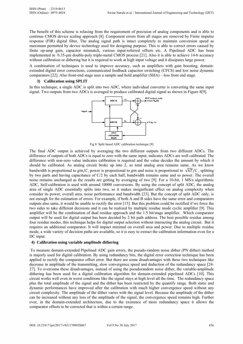
3) Calibration using SPLIT
In this technique, a single ADC is split into two ADC, where individual converter is converting the same input signal. Two outputs from two ADCs is averaged to produce calibrated digital signal as shown in Figure 8[9].
Fig 8: Split based ADC calibration technique [9]
The final ADC output is achieved by averaging the two different outputs from two different ADCs. The difference of outputs of both ADCs is equal to zero with the same input, indicates ADCs are well calibrated. The difference with non-zero value indicates calibration is required and the value decides the amount by which it should be calibrated. As analog circuit broke up into 2, so total analog area remains same. As we know bandwidth is proportional to / , power is propostional to and noise is proportional to √ / , splitting by two parts and having capacitance of C/2 by each half, bandwidth remains same and so power. The overall noise remains unchanged as the results are getting by averaging of two [9]. For a 10-bit, 1 MS/s algorithmic ADC, Self-calibration is used with around 10000 conversions. By using the concept of split ADC, the analog area of single ADC essentially splits into two, so it makes insignificant effect on analog complexity when consider its power, overall area, noise performance and bandwidth [23]. But the concept of split ADC only, is not enough for the estimation of errors. For example, if both A and B sides have the same error and comparators outputs also same, it would be unable to rectify the error [15]. But this problem could be rectified if we force the two sides to take different decisions and it can be realized by multiple residue mode cyclic amplifier [9]. This amplifier will be the combination of dual residue approach and the 1.5 bit/stage amplifier. Which comparator output will be used for digital output has been decided by 2 bit path address. The best possible residue among four residue modes, this technique helps for digital output selection without interacting the analog circuit. But it requires an additional comparator. It will impact minimal on overall area and power. Due to multiple residue mode, a wide variety of decision paths are available, so it is easy to extract the calibration information even for a DC input.
4) Calibration using variable amplitude dithering
To measure domain-extended Pipelined ADC gain errors, the pseudo-random noise dither (PN dither) method is majorly used for digital calibration. By using redundancy bits, the digital error correction technique has been applied to rectify the comparator offset error. But there are some disadvantages with these two techniques like decrease in amplitude of the transmitting, slow convergence speed and deduction of the redundancy space [24-27]. To overcome these disadvantages, instead of using the pseudorandom noise dither, the variable-amplitude dithering has been used for a digital calibration algorithm for domain-extended pipelined ADCs [10]. This circuit works well even in worst conditions like the signal stays at high level all the time. The redundancy space plus the total amplitude of the signal and the dither has been restricted by the quantify range. Both static and dynamic performances have improved after the calibration with much higher convergence speed without any circuit complexity. The amplitude of the dither varies with the signal level. Because the amplitude of the dither can be increased without any loss of the amplitude of the signal, the convergence speed remains high. Further over, in the domain-extended architecture, due to the existence of more redundancy space it allows the comparator offsets to be corrected that is within a certain range.
ISSN (Print) : 2319-8613 ISSN (Online) : 0975-4024 Swina Narula et al. / International Journal of Engineering and Technology (IJET)
DOI: 10.21817/ijet/2017/v9i3/170903S067 Vol 9 No 3S July 2017 436
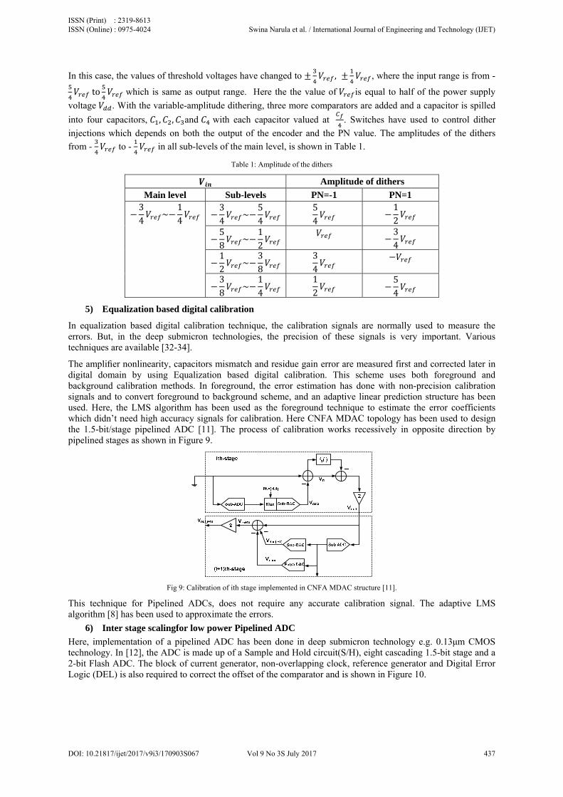
In this case, the values of threshold voltages have changed to , , where the input range is from -
to which is same as output range. Here the the value of is equal to half of the power supply
voltage . With the variable-amplitude dithering, three more comparators are added and a capacitor is spilled
into four capacitors, , , and with each capacitor valued at . Switches have used to control dither
injections which depends on both the output of the encoder and the PN value. The amplitudes of the dithers
from - to - in all sub-levels of the main level, is shown in Table 1.
Table 1: Amplitude of the dithers
Amplitude of dithers
Main level Sub-levels PN=-1 PN=1 3
4~
1
4
3
4~
5
4
5
4
1
2
5
8~
1
2
3
4
1
2~
3
8
3
4
3
8~
1
4
1
2
5
4
5) Equalization based digital calibration
In equalization based digital calibration technique, the calibration signals are normally used to measure the errors. But, in the deep submicron technologies, the precision of these signals is very important. Various techniques are available [32-34].
The amplifier nonlinearity, capacitors mismatch and residue gain error are measured first and corrected later in digital domain by using Equalization based digital calibration. This scheme uses both foreground and background calibration methods. In foreground, the error estimation has done with non-precision calibration signals and to convert foreground to background scheme, and an adaptive linear prediction structure has been used. Here, the LMS algorithm has been used as the foreground technique to estimate the error coefficients which didn’t need high accuracy signals for calibration. Here CNFA MDAC topology has been used to design the 1.5-bit/stage pipelined ADC [11]. The process of calibration works recessively in opposite direction by pipelined stages as shown in Figure 9.
Fig 9: Calibration of ith stage implemented in CNFA MDAC structure [11].
This technique for Pipelined ADCs, does not require any accurate calibration signal. The adaptive LMS algorithm [8] has been used to approximate the errors.
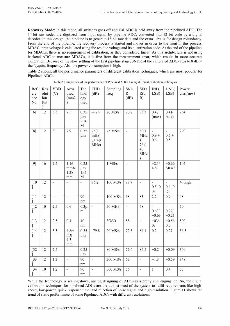
6) Inter stage scalingfor low power Pipelined ADC
Here, implementation of a pipelined ADC has been done in deep submicron technology e.g. 0.13μm CMOS technology. In [12], the ADC is made up of a Sample and Hold circuit(S/H), eight cascading 1.5-bit stage and a 2-bit Flash ADC. The block of current generator, non-overlapping clock, reference generator and Digital Error Logic (DEL) is also required to correct the offset of the comparator and is shown in Figure 10.
ISSN (Print) : 2319-8613 ISSN (Online) : 0975-4024 Swina Narula et al. / International Journal of Engineering and Technology (IJET)
DOI: 10.21817/ijet/2017/v9i3/170903S067 Vol 9 No 3S July 2017 437
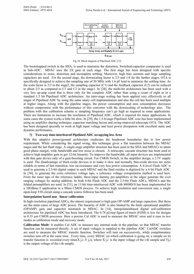
Fig 10: Block diagram of Pipelined ADC [12]
The bootstrapped switch in the SHA, is used to minimize the distortion. Switched-capacitor comparator is used in Sub-ADC. MDAC uses the 2X gain in each stage. The first stage has been designed with specific considerations to noise, distortion and incomplete settling. Moreover, high bias currents and large sampling capacitors are used. For the second stage, the downscaling factor is 2/3 and 1/4 for the further stages. OTA is specifically designed to achieve the sampling rate of 50 MHz with 1.6 pF load to minimize the settling time. As the scale factor is 2/3 in the stage2, the sampling capacitor (C1) and the feedback capacitor (C2) can be reduced to about 2/3 as compared to C1 and C2 in the stage1. In [28], the multi-bit architecture has been used with a very less op-amp count that is three only for the complete ADC rather than using a count of eight as in a standard 1.5 bit Pipelined ADC architecture. An inter-stage scaling has been applied very effectively to all stages of Pipelined ADC by using the same unary cell implementation and also the cell has been used multiple at higher stages. Along with the pipeline stages, the power consumption and area consumption decreases without compromise with the performance of this converter with the downscaling of technology also. The problem with this calibration scheme is sampling frequency can’t go high as required in some applications. There are limitations to increase the resolution of Pipelined ADC, which is required for many applications. In some cases the system works a little bit slow. In [29], the 1.5-b/stage Pipelined ADC core has been implemented using an amplifier sharing technique, capacitor matching layout and swing-improved telescopic OTA. The ADC has been designed specially to work at high input voltage and least power dissipation with excellent static and dynamic performance.
7) Two-way time-interleaved Pipelined ADC occupying less Area
With this adaptive power/ground architecture eradicates the headroom boundaries due to low power requirement. While considering the signal swing, this technique gives a flat transition between the MDAC stages and the last flash stage. A single-stage amplifier structure has been used in the SHA and MDACs to attain good phase margin, wide bandwidth and low noise is chosen. A telescopic cascade structure has been used to achieve high amplifier gain to get 12-bit linearity. To improve the bandwidth, all input devices are implemented with thin gate device only of a gain-boosting circuit. For CMOS Switch, in the amplifier design, a 2.5V supply is used. The disadvantage of thick-oxide devices is to make it slow and normally thin-oxide devices are more reliable in terms of fast transition, low on-resistance and very less power consumption. A 6-level Flash ADC is used to generate a 2.5-bit digital output in each MDAC and the final residue is digitized by a 6 bit Flash ADC. In [30], to generate the extra reference voltage taps, a reference voltage extrapolation method is used here. From the inner taps of the reference ladder, three-input dummy pre-amplifiers at the edges generate the over ranging voltages by analog addition. In both 6-bit Flash ADC and the 2.5-bit Flash ADCs, MDACs and the folded preamplifiers are used. In [31], an 11-bit time-interleaved ADC with 800MS/S has been implemented for a 10GBase-T application in a 90nm CMOS process. To achieve high resolution and conversion rate, a single open-loop T/H circuit using a cascade source follower has been used.
Interpolation based non - linear calibration
In high resolution pipelined ADCs, the utmost requirement is high gain OP-AMP and large capacitors. But these are the main cause of large ADC power. The linearity of ADC is also limited by the finite operational amplifier (OPAMP) gain and capacitor mismatch in MDAC. In [14], interpolationbased digital self-calibration architecture for pipelined ADC has been introduced. The 0.78 pJ/step figure-of-merit (FOM) is low for designs in 0.35 µm CMOS processes. Here a precise Cal ADC is used to measure the MDAC error and it runs in two modes as calibration mode and recovery mode.
Calibration Mode: It enables Cal ADC to measure any internal node in the pipeline, so that MDAC transfer function can be measured directly. A set of input voltages is supplied to the pipeline ADC. CalADC switches are used to measure the MDAC transfer function. Switches will turn on successively, while complimentary switches turn off at the same time. Every time, every MDAC on which calibration is going on, a sample on its transfer function is recorded every time(X j,i ,Y j,i), where X j,i is the input voltage of the i-th sample and Yj,i is the output voltage of the i-th sample.
ISSN (Print) : 2319-8613 ISSN (Online) : 0975-4024 Swina Narula et al. / International Journal of Engineering and Technology (IJET)
DOI: 10.21817/ijet/2017/v9i3/170903S067 Vol 9 No 3S July 2017 438
Recovery Mode: In this mode, all switches goes off and Cal ADC is held away from the pipelined ADC. The 14-bit raw codes are digitized from input signal by pipeline ADC, converted into 12 bit code by a digital decoder. In this design, the pipeline is to generate 13-bit raw data and the extra 1-bit is for design redundancy. From the end of the pipeline, the recovery process is started and moves in order to the front in this process, MDAC input voltage is calculated using the residue voltage and its quantization code. At the end of the pipeline, for MDACs, there is no requirement of calibration, as they considered linear. As this architecture is not using backend ADC to measure MDACs, it is free from the measurement error, which results in more accurate calibration. Because of the slow settling of the first pipeline stage, SNDR of the calibrated ADC drips to 8 dB at the Nyquist frequency. Also the power consumption is high.
Table 2 shows, all the performance parameters of different calibration techniques, which are most popular for Pipelined ADCs.
Table 2: Comparison of the performance of Pipelined ADCs having different calibration techniques
Reference No.
Resolution (bit)
VDD (V)
Area used (mm2)
Technology used
THD (dB)
Sampling freq
SNDR (dB)
SFDR(dB)
INL(LSB)
DNL(LSB)
Power diss.(mw)
[6] 12 3.3 7.5 0.35 µm 2P4M
–92.9 20 MS/s 70.8 93.3 0.47 (max)
0.41(max)
254
[8] 12 3 7.9 0.35 µm
76(1 mHz) 74(40 MHz)
75 MS/s - 80(1 MHz) 76 ( 40 MHz)
-0.9,+0.6
-0.5,+0.5
290
[9] 16 2.5 1.16mmX1.38mm
0.25 µm 1P4M
1 MS/s - - +2.1/-4.8
+0.66/-0.47
105
[10]
12 - - - 86.2 100 MS/s 87.7 - -0.5~0.4
-0.4~0.5
V. high
[11]
12 - - 90 nm
- 100 MS/s 68 83 2.2 0.9 48
[12]
10 2.5 0.6 0.3µm
- 50 MHz - 68 -0.63/+0.63
-0.27/+0.21
50
[13]
12 2.5 0.4 40 nm
3GS/s 58 - +03/-03
+0.5/-0.5
500
[14]
12 3.3 4.8mmX 4.3 mm
0.35 µm
-79.8 20 MS/s 72.5 84.4 0.2 0.27 56.3
[32]
12 2.5 - 0.25 µm
- 80 MS/s 72.6 84.5 +0.24 +0.09 340
[33]
12 1.2 - 90 nm
- 200 MS/s 62 - +1.3 +0.59 348
[34]
10 1.2 - 90 nm
- 500 MS/s 56 - 1 0.4 55
While the technology is scaling down, analog designing of ADCs is a pretty challenging job. So, the digital calibration techniques for pipelined ADCs are the utmost need of the system to fulfil requirements like high-speed, low-power, quick response time, and rejection of noise signal and high-resolution. Figure 11 shows the trend of static performance of some Pipelined ADCs with different resolutions.
ISSN (Print) : 2319-8613 ISSN (Online) : 0975-4024 Swina Narula et al. / International Journal of Engineering and Technology (IJET)
DOI: 10.21817/ijet/2017/v9i3/170903S067 Vol 9 No 3S July 2017 439
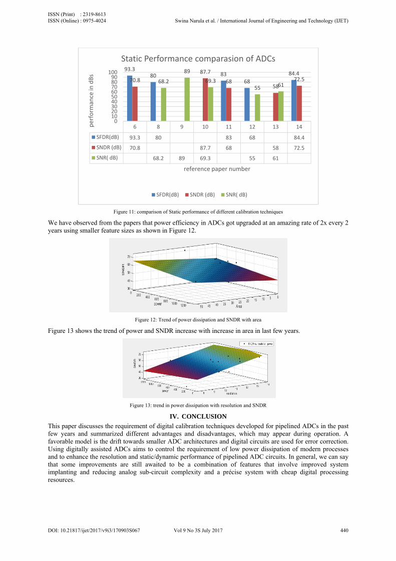
Figure 11: comparison of Static performance of different calibration techniques
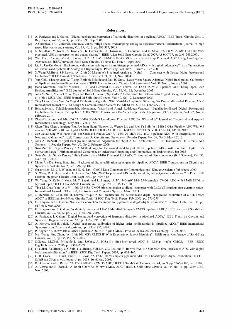
We have observed from the papers that power efficiency in ADCs got upgraded at an amazing rate of 2x every 2 years using smaller feature sizes as shown in Figure 12.
Figure 12: Trend of power dissipation and SNDR with area
Figure 13 shows the trend of power and SNDR increase with increase in area in last few years.
Figure 13: trend in power dissipation with resolution and SNDR
IV. CONCLUSION
This paper discusses the requirement of digital calibration techniques developed for pipelined ADCs in the past few years and summarized different advantages and disadvantages, which may appear during operation. A favorable model is the drift towards smaller ADC architectures and digital circuits are used for error correction. Using digitally assisted ADCs aims to control the requirement of low power dissipation of modern processes and to enhance the resolution and static/dynamic performance of pipelined ADC circuits. In general, we can say that some improvements are still awaited to be a combination of features that involve improved system implanting and reducing analog sub-circuit complexity and a précise system with cheap digital processing resources.
6 8 9 10 11 12 13 14
SFDR(dB) 93.3 80 83 68 84.4
SNDR (dB) 70.8 87.7 68 58 72.5
SNR( dB) 68.2 89 69.3 55 61
93.380 83
68
84.470.8
87.7
6858
72.568.2
89
69.355 61
0102030405060708090
100
perform
ance in dBs
reference paper number
Static Performance comparasion of ADCs
SFDR(dB) SNDR (dB) SNR( dB)
ISSN (Print) : 2319-8613 ISSN (Online) : 0975-4024 Swina Narula et al. / International Journal of Engineering and Technology (IJET)
DOI: 10.21817/ijet/2017/v9i3/170903S067 Vol 9 No 3S July 2017 440
References:
[1] A. Panigada and I. Galton, “Digital background correction of harmonic distortion in pipelined ADCs,” IEEE Trans. Circuits Syst. I, Reg. Papers, vol. 53, no. 9, pp. 1885–1895, Sep. 2006.
[2] A.Gharbiya, T.C. Caldwell, and D.A. Johns, “High speed oversampling analog-to-digitalconverters,” International journal of high speed Electronics and systems, Vol. 15, No. 2, pp. 297-317, 2005.
[3] N. Sasidhar , Y. Kook , S. Takeuchi , K. Hamashita , K. Takasuka , P. Hanumolu and U. Moon "A 1.8 V 36-mW 11-bit 80 MS/s pipelined ADC using capacitor and opamp sharing", IEEE Asian Solid-State Circuits Conf. 2007, ASSCC\'07, pp.240 -243 2007 .
[4] Wu, P.Y., Cheung, V.S.-L. ; Luong, H.C. “A 1-V 100-MS/s 8-bit CMOS Switched-Opamp Pipelined ADC Using Loading-Free Architecture” IEEE Journal of Solid-State Circuits, Volume 42 , Issue 4, April 2007.
[5] Li, J. ; Un-Ku Moon “Background calibration techniques for multistage pipelined ADCs with digital redundancy” IEEE Transactions on Circuits and Systems II: Analog and Digital Signal Processing, Volume:50 , Issue: 9 , Sep 2003
[6] X.Wang,P.J.Hurst, S.H.Lewis, “A 12-bit 20-Msample/s Pipelined Analog-to-Digital Converter with Nested Digital background Calibration”, IEEE Journal of Solid-State Circuits, vol.39, No.11, Nov. 2004.
[7] Yun Chiu, Cheong yuen W. Tsang, Borivoje Nikolic and Paul R. Gray, “Least Mean Square Adaptive Digital Background Calibration of Pipelined Analog-to-Digital Converters “IEEE Transactions On Circuits And Systems—I Vol. 51, No. 1, January 2004 .
[8] Boris Murmann, Student Member, IEEE, and Bernhard E. Boser, Fellow, “A 12-bit 75-MS/s Pipelined ADC Using Open-Loop Residue Amplification” IEEE Journal of Solid-State Circuits, Vol. 38, No. 12, December 2003.
[9] John McNeill, Michael C. W. Coln and Brian J. Larivee,“Split ADC” Architecture for Deterministic Digital Background Calibration of a 16-bit 1-MS/s ADC “IEEE Journal Of Solid-State Circuits, Vol. 40, No. 12, December 2005
[10] Ting Li and Chao You “A Digital Calibration Algorithm With Variable-Amplitude Dithering For Domain-Extended Pipeline Adcs” International Journal of VLSI design & Communication Systems (VLSICS) Vol.5, No.1, February 2014
[11] BehzadZeinali, TohidMoosazadeh, Mohammad Yavari and Angel Rodriguez-Vazquez, “Equalization-Based Digital Background Calibration Technique for Pipelined ADCs “IEEE Transactions On Very Large Scale Integration (VLSI) Systems, Vol. 22, No. 2, February 2014
[12] Zhzo-Xin Xiong and Min Cai “A 10-Bit 50-Ms/S Low-Power Pipeline ADC For Wimax/Lte” Journal of Theoretical and Applied Information Technology , May 2013. Vol. 51 No.3
[13] Chun-Ying Chen, Jiangfeng Wu, Juo-Jung Hung, Tianwei Li, Wenbo Liu and Wei-Ta Shih “A 12-Bit 3 GS/s Pipeline ADC With 0.4 mm and 500 mW in 40 nm Digital CMOS” IEEE JOURNALOFSOLID-STATECIRCUITS, VOL.47, NO.4, APRIL 2012
[14] JieYuan,Sheung Wai Fung, Kai Yin Chan and Ruoyu Xu “A 12-bit 20 MS/s 56.3 mW Pipelined ADC With Interpolation-Based Nonlinear Calibration” IEEE Transactions On Circuits And Systems—I: Regular Papers, Vol. 59, No. 3, March 2012
[15] John A. McNeill, “Digital Background-Calibration Algorithm for “Split ADC” Architecture”, IEEE Transactions On Circuits And Systems—I: Regular Papers, Vol. 56, No. 2, February 2009.
[16] SwinaNarula , Sujata Pandey “ A Methodology for Behavioral modeling of 10 bit Pipelined ADCs with modified Digital Error Correction Logic” Fifth international Conference on Advanced Computing and Communication Technologies, Jan 2015
[17] SwinaNarula, Sujata Pandey “High Performance 14-Bit Pipelined RSD ADC.” inJournal of Semiconductors (IOP Science), Vol. 37, No.3, pp. , 2016.
[18] Moon, Un-Ku. Song, Bang-Sup. “Background digital calibration techniques for pipelined ADCs”, IEEE Transactions on Circuits and Systems II- Vol. 44, No. 2, Feb 1997, pp 102.
[19] Gustavsson, M., J. J. Wikner, and N. N. Tan, “CMOS Data Converters for Communications” Kluwer Academic Publishers, 2000. [20] X. Wang, P. J. Hurst, and S. H. Lewis, “A 12-bit 20-MS/s pipelined ADC with nested digital background calibration,” in Proc. IEEE
Custom Integrated Circuits Conf., Sept. 2003, pp. 409–412. [21] W. Yang, D. Kelly, I. Mehr, M. T. Sayuk, and L. Singer, “A 3-V 340-mW 14-b 75-Msample/s CMOS ADC with 85-dB SFDR at
Nyquist input,” IEEE J. Solid-State Circuits, vol. 36, pp. 1931–1936, Dec. 2001. [22] Ting Li, Chao You “A 3-V 14-bit 75-MS/s CMOS pipeline analog-to-digital converter with 93.72-dB spurious-free dynamic range”
International Journal of Electrical, Electronics and Computer Systems, March 2014. [23] J. McNeill, M. Coln, and B. Larivee, ““Split-ADC” architecture for deterministic digital background calibration of a 16b 1MS/s
ADC,” in IEEE Int. Solid-State Circuits Conf. (ISSCC) Dig. Tech. Papers, Feb. 2005, pp. 276–278. [24] E. Siragusa and I. Galton, “Gain error correction technique for pipelined analog-to-digital converters,” Electron. Letter, vol. 36, pp.
617–618, Mar. 2000. [25] E. Siragursa and I. Galton, “A digitally enhanced 1.8-V 15-bit 40-MSample/s CMOS pipelined ADC,” IEEE Journal of Solid-State
Circuits, vol. 39, no. 12, pp. 2126–2138, Dec. 2004. [26] A. Panigada, I. Galton. “Digital background correction of harmonic distortion in pipelined ADCs,” IEEE Trans. on Circuits and
Systems I: Regular Papers, vol. 53, pp. 1885–1895, 2006. [27] A. Meruva, and B. Jalali, “Digital background calibration of higher order nonlinearities in pipelined ADCs,” IEEE International
Symposium on Circuits and Systems, pp. 1233–1236, 2007. [28] P. Bogner, “A 28mW 10b 80MS/s Pipelined ADC in 0.13 µm CMOS”, Proc. of the ISCAS 2004 Conf., pp. 17–20, 2004. [29] Nan Wang, Ping Zhou, “A 10-bit 100-MS/s CMOS IP With Emphasis on layout Matching” , IEEE Asian Conference of Solid-State
Circuits, vol. 12, pp.335-358, Nov 2006. [30] S.Gupta, M.Choi, M.Inerfield, and J.Wang,“A 1GS/s11b time-interleaved ADC in 0.13/spl mu/m CMOS,” IEEE ISSCC
Dig.Tech.Papers , 2006, pp. 2360–2369 [31] C.-C.Hsu, F.C.Huang, C.Y.Shih, C.C.Huang, Y.H.Lin, C.C.Lee, and B. Razavi, “An 11b 800 MS/s time-interleaved ADC with digital
back ground calibration,” in IEEE ISSCC Dig. Tech. Papers, 2007, pp. 464–465. [32] C. R. Grace, P. J. Hurst, and S. H. Lewis, “A 12-bit 80-MSample/s pipelined ADC with bootstrapped digital calibration,” IEEE J.
SolidState Circuits, vol. 40, no. 5, pp. 1038–1046, May 2005. [33] B. D. Sahoo and B. Razavi, “A 12-bit 200-MHz CMOS ADC,” IEEE J. Solid-State Circuits, vol. 44, no. 9, pp. 2366–2380, Sep. 2009. [34] A. Verma and B. Razavi, “A 10-bit 500-MS/s 55-mW CMOS ADC,” IEEE J. Solid-State Circuits, vol. 44, no. 11, pp. 3039–3050,
Nov. 2009.
ISSN (Print) : 2319-8613 ISSN (Online) : 0975-4024 Swina Narula et al. / International Journal of Engineering and Technology (IJET)
DOI: 10.21817/ijet/2017/v9i3/170903S067 Vol 9 No 3S July 2017 441