o/lzAlt& ,1 TURBO-XT Main Board InstallatIon GuIde Main Board - Installation... · The heart of the...
32
,1 o /lzAlt&- TURBO-XT Main Board InstallatIon GuIde
-
Upload
doannguyet -
Category
Documents
-
view
231 -
download
0
Transcript of o/lzAlt& ,1 TURBO-XT Main Board InstallatIon GuIde Main Board - Installation... · The heart of the...
,1o/lzAlt&TURBO-XT Main Board InstallatIon GuIde
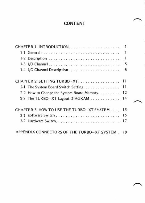
CONTENT
CHAPTER 1 INTRODUCTION.................... .
1-1 General ............................... .
1-2 Description ............................ .
1-3 I/O Channel. . . . . . . . . . . . . . . . . . . . . . . . . . . .. 5
1-4 I/O Channel Description. . . . . . . . . . . . . . . . . . . .. 6
CHAPTER 2 SETTING TURBO-XT. . . . . . . . . . . . . . . .. 11
2-1 The System Board Switch Setting. . . . . . . . . . . . . .. 11
2-2 How to Change the System Board Memory. . . . . . . .. 12
2-3 The TURBO-XT Lagout DIAGRAM ............ 14
CHAPTER 3 HOW TO USE THE TURBO-XT SYSTEM .... 15
3-1 Software Switch. . . . . . . . . . . . . . . . . . . . . . . . .. 15
3-2 Hardware Switch. . . . . . . . . • . . . . . . . . . . . . . . .. 17
APpENDIX CONNECTORS OF THE TURBO-XT SYSTEM. 19
CHAPTER 1 INTRODUCTION
1-1 General
The TURBO-XT is an Intel 8088-2 microprocessor-based sys
tem. It can run the most popular software packages like WORD
STAR, DBASEII, LOTUS 1-2-3, AUTOCAD, SYMPHONY and so
on. But please note use Normal mode (4.77 MHz) When running
copy WRITE.
The following manual will provide detailed functions and using
for TURBO-XT.
1-2 Description
The TURBO--XT system board fits horizontally in the base of
the system unit and is approximately 81/2 12 inches. It is two
layer P.c.B. DC power and a signal from the power supply enter
the board through 12 pin connectors. Other connectors on the
board are for attaching the keyboard and speaker. Eight 62-pin
card edge-sockets are also mounted on the board. The I/O channel
is bussed across these eight I/O slots.
A dual-in-line package (DI P) switch (SWI) (one eightswitch
pack) is mounted on the board and can be read under program
control, The DIP switch provides the system software with in
formation about the installed options, how much storage the
system board has, what type of the display adapter is install-led,
what operation modes are disired when power is switched on (color
or black-and-white, 80-or 40-character lines), and the number of
diskette drive attached.
The system board consists of five functional area: the pro
cessor subsystem and its support elements, the read-only mormory
(ROM) subsystem, the read/write (R/W) memory subsystem,
integrated I/O adapters, and the I/O channel. All are desired in
this section.
The heart of the TU RBO-XT system board is the In tel 8088-2
micro-processor. This pocessor is an 8- bit external bus version of
Intel's 16-bit 8086 processor, and is software-compatible with
the 8086. Thus, the 8088-2 supports 16-bit operations, including
mUltiply and divide. It also operates in maximum mode, so a
coprocessor can be added as a feature. In normal mode. The pro
cessor operates at 4.77 MHz. This frequency, which is derived
from a 14.318 MHz crystal. When you change mode to tu rbo
mode. Will give you an increase of almost 70% in speed of program
execution. At the time, the pro-cessor operates at 8MHz.
The processor is supported by a set of high-function support
2

devices providing four channels of 20-bit direct-mem~ry access
(DMA), three 16-bit timer-counter channels, and eight tlrioritized
interrupt levels.
Three of the four DMA channels are available on the I/O bus
and support high speed data transfers between I/O devices and
memory without processor intervention. The fourth DMA channel
is programmed to. refresh the system dynamic memory. This is
done by programming a channel of the timer-counter divice to
periodically request a dummy DMA transfer. This action creates a
memory-read cycle, which is available to refresh dynamic storage
both on the system board and in the system expansion slots.
The three programmable timer/counters are used by the
system as follows: Channel 0 is used as a general-purpose timer
providing a constant time base for implementing a time-of-day
clock; Channel 1 is used to time and request refresh cycles from
the DMA channel; and Channel 2 is used to support the tone
generation for the audio speaker.
Of the eight prioritized levels of interrupt, six are bussed to
the system expansion slots for use by features cards. Two levels
are used on the system board. Level 0, the highest priority, is
attached to Channel 0 of the timer/counter and provides a periodic
interrupt for the time-af-day clock. Level 1 is attached to the
keynoard adapter circuits and receives an interrupt of each scan
3
code sent by the keyboard. The non-maskable interrupt (NMI) of
the 8088-2 is used to report memory parity errors.
The system board supports both ROM/EPROM and R/W
memory. It has space for 64K x 8 of ROM or EPROM. This
ROM contains the power-<>n self-test, I/O drivers, dot patterns for
128 characters in graphics mode, and It also has of 64K R/W
memory. Memory greater than the system board has a maximum
of all R/W memery is parity checked.
The system board contains the adapter circuits for attaching
the serial· interface from the keyboard. These circuits generate an
interrupt to the processor when a complete scan code is received.
The interface can request execution of a diagnostic test in the key
board.
The keyboard interface is a 5-pin DIN connector on the
system board that extends through the rear panel of the system
unit.
The system units has an 2-1/4 inch audio speaker. The spea
ker's control circuits and driver are on the system board. The
speaker connects through a 2-wire interface that attaches to a 3-pin
connector on the system board.
The speaker drive circuit is capable of approximately 1/2 watt
4
of power. The control circuits allow the speaker to be driven three
different way: 1) a direct program control register bit may be
toggled to generate a pulse train; 2) the output from Channel 2 of
the timer cOIJnter may be programmed to generate a waveform to
to speaker; 3) the clock input to the timer counter car1 be mo
dulated with a program-controlled I/O register bit. All three
methods may be performed simultaneously.
The TURBO-XT has the following components
* I n tel 8088-2 microprocesso r.
* Socket for 8087-2 math co-processor.
* Either a 256 KB or a 640 KB random-access memory (RAM)
subsystem.
* Running at 4.77 MHz (8 MHa option).
* 8 input/ouput (I/O) slots with 62-pins card-edge socket.
* Disk Storage:
-Base Model: two 5-1/4" floppy disk drive with 360 KB.
-Enhanced Model: can add one 20 MB Harddisk drive.
1-3 I/O Channel
The I/O channel is an extension of the 8088-2 microprocessor
bus. It is, however, demultiplexed, repowered, and enhance by the
addition of interrupts and direct memory access (DMA) functions.
5
The I/O channel contains an 8 bit, bidirectional data bus, 20
address lines, 6 levels of interrupt, control lines for memory and
I/O read or write, clock and timing lines, 3 channels of DMA
control lines, memory refresh timing control lines, a channel check
line, and power and ground for the adapters.
I/O devices are addressed using I/O mapped address space.
The chan nel is designed so that 768 I/O device addressed are
abailable to the I/O channel cards.
A channel check line exists for reporting error conditions to
the processor. Activating this line results in a Non-Maskable In
terrupt (NMI) to the 8088-2 processor. Memory expansion options ,,--.....,
use this line to report parity errors.
1-4 I/O Channel Description
The following is a description of the I/O Channel. All lines
are TIL-compatible.
Singall/O Description:
OSC, Oscillator:
High speed clock with a 70-ns period (14.31818 MHz). it has
a 50% duty cycle.
ClK, System Clock:
6
It is divide-by-three of the oscillator and has a period of 210 ns
(4.77 MHz). The clock has a 33% duty cycle.
RESET:
This line is used to reset or initialize system logic upon power
up or. during a low line voltage outage. This signal is synchronized
to the falling edge of clock and is active high.
AO-A19, Address Bits 0 to 19:
These lines are used to address memory and I/O devices within
the system. The 20 address lines allow access of up to 1 megabyte
of memory. AO is the Least Significant Bit (LSB) and A19 is the
"........." Most Significant Bit (MSB). These lines are generated by either
the processor or OMA controller. They are active high.
00-07, I/O Oata Bits 0 to 7:
These lines provide data bus bits 0 to 7 for the processor,
memory, and I/O devices. 00 is the Least Significant Bit (LSB)
and 07 is the MoS( Significant Bit (MSB). These lines are active
high.
ALE, Address Latch Enable:
This line is provided by the 8288 Bus Controller and is used on
the system board to latch valid addresses from the processor. It
is available to the I/O channel as an indicator of a varid processor
address (When used with AEN). Processor addresses are la~ched
7
with the failing edge of ALE.
I/O CH CK, I/O Channel Check: .
This line provides the processor with parity (error) in for ma
tion on memory or devices i.n the I/O channel. When this signal is
active low, a parity error would indicated.
I/O CH RDY, I/O Channel Ready:
This line, normally high (ready), can be pulled low (not ready)
by a memory or I/O device to lengthen I/O or memory cycles.
It allows slower devices to attacheh to the I/O channel with a
minimum of difficulty. Any slow device using this line should
drive it low immediately upon detecting a valid address and a read ~
or write command. This lines should never be held low, longer
than 10 clock cycles. Machine cycles (I/O or memory) are exten
ded by an integral number of ClK cycles (210 ns).
IRQ2-1 RQ7,Interrupt Request 2 to 7:
. These lines are used to signal the processor, that a I/O device
requires attention. They are prioritized with I RQ2 as the highest
priority and I RQ7 as the lowest. An· Interrupt Reguest is gene
rated by raising an I RQ line (low to high) and holding it high, until
it was acknowledged by the processor (interrupt service routine).
lOR, I/O Read Command:
This command line instructs an I/O device to drive its data
8
into the data bus. It may be driven by the processor or the DMA
controller. This signal is active low.
LOW, I/O Write Command:
The command line instructs an I/O device, to read the data on
the data bus. It may be driven by the processor or the DMA
controller. This signal is active low.
MEMR, M~mory Read Command:
This;command line instructs the memory to drive its data into
the data bus. It may .be driven by.the processor or the DMA
controller. Th is signal is active low.
MEMW, Memory Write Command:
This command line instructs the memory to store the data
present on the data bus. It may be driven by the processor or
the DMA controller. This signal is active low.
DRQ1-DRQ3, DMA Request 1 to 3:
These lines are asynchronous channel requests used by peri
pheral devices to gain DMA service. They are prioritized with
DRQ3 being the lowest and DRQl being the highest. A request is
generated by bringing a JRQ line to an active level (high). A DRQ
line must be held high until the corresponding DACK line goes·
active.
9
DACKO-3-DMA Acknowledge 0 to 3:
These lines are DACK3 used to acknowledge DMA requests
(DRQ1-DRQ3) and to refresh system dynamic memory (DACKO).
They are active low.
AEN, Address Enable:
This line is used to degate the processor and other devices
from the I/O channel to allow DMA transfers to take place. When
this line is active (high), the DMA controller has control the ad
dress bus, data bus, read command lines (memory and I/O), and
the write command lines (memory and I/O).
T/C, Terminal Count:
This line provides a pulse when the terminal count for any
DMAchannel is reached. This signal is active high.
10
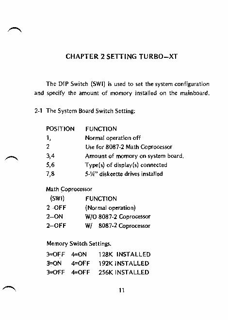
CHAPTER 2 SETTING TURBO-XT
The DIP Switch (SWI) is used to set the system configuration
and specify the amount of momory installed on the main board.
2-1 The System Board Switch Setting:
POSITION FUNCTION
1, Normal operation off
2 Use for 8087-2 Math Coprocessor
3,4 Amount of momory on system board.
5,6 T ype(s) of dispJay(s) connected
7,8 5-W' diskeette drives installed
Math ~processor
(SWi) FUNCTION
2-0FF (Normal operation)
2-0N W/O 8087-2 Coprocessor
2-0FF WI 8087-2 Coprocessor
Memory Switch Settings.
3=OFF 4=ON 128K INSTALLED
3=ON 4=OFF 1921< INSTALLED
3=OFF 4=OFF 256K INSTALLED
11
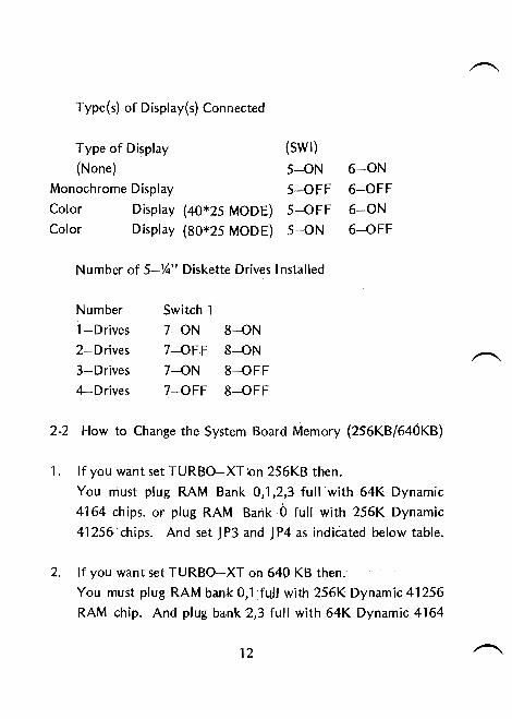
Type(s) of Display(s) Connected
Type of Display (SWI)
(None) 5-0N 6-0N
Monochrome Display 5-0FF 6-0FF
Color Display (40*25 MODE) 5--OFF 6-0N
Color Display (80*25 MODE) 5-0N 6-0FF
Number of5-%" Diskette Drives Installed
Number Switch 1
1-Drives 7-0N &-ON
2-Drives 7-0FF 8-0N
3-Drives 7-0N 8-0FF
4-Drives 7-0FF 8-0FF
2-2 How to Change the System Board Memory (256KB!640KB)
1. If you want set TURBO-XT:on 256KBthen.
You must plug RAM Bank 0,1,2,3 full with 64K Dynamic
4164 chips. or plug RAM Bank () full with 256K Dynamic
41256'chips. And set JP3 and JP4 as indiCated below table.
2. If you want set TURBO-XT on 640KB then.
You must plug RAM bank 0,1 full with 256K Dynamic 41256
RAM chip. And plug bank 2,3 full with 64K Dynamic 4164
12
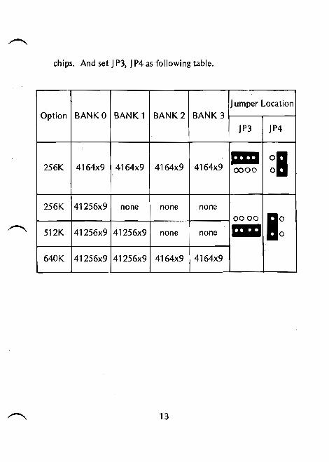
chips. And set JP3, JP4 as following table.
Jumper Location
Option BANKO BANK 1 BANK2 BANK 3
JP3 JP4
II1II ~I256K 4164x9 4164x9 4164x9 4164x9 0000
256K 41256x9 none none none 0000
512K 41256x9 41256x9 none none Ii'" I: 640K 41256x9 41256x9 4164x9 4164x9
13
".\
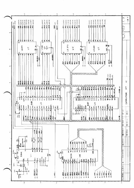
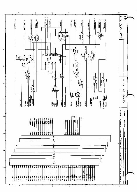
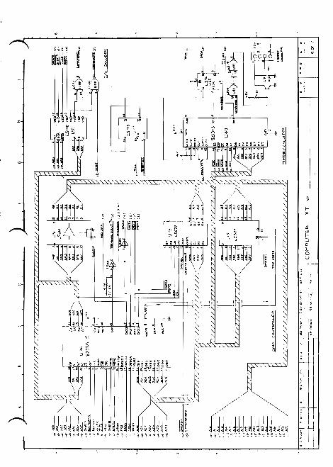
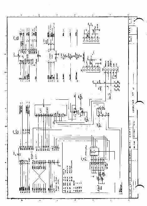
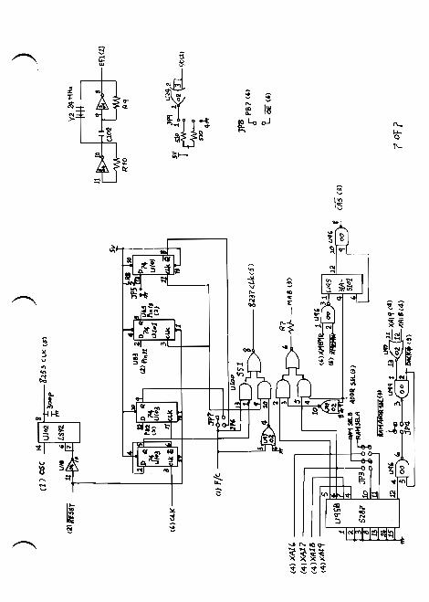
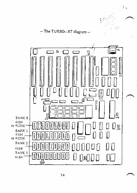
- The TURBO-XT diagram
14
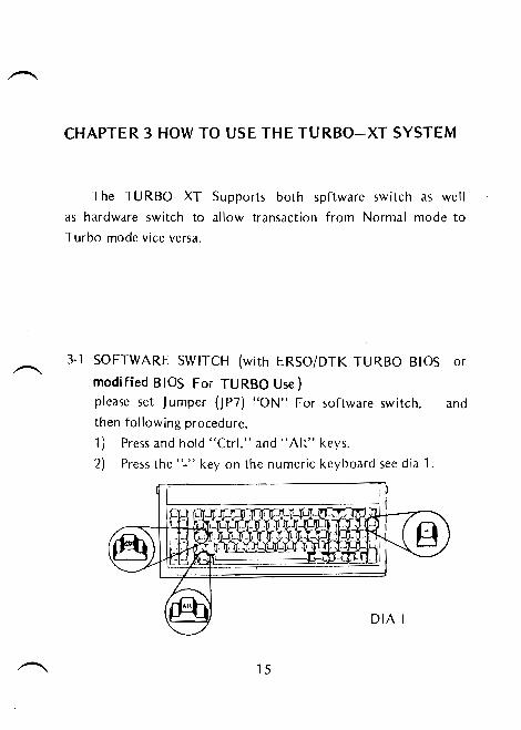
CHAPTER 3 HOW TO USE THE TURBO-XT SYSTEM
The TURBO-XT Supports both spftware switch as well
as hardware switch to allow transaction from Normal mode to Turbo mode vice versa.
3-1 SOFTWARE SWITCH (with ERSO/DTK TURBO BIOS or
modified BIOS For TURBO Use)
please set Jumper (j P7) "ON" For software switch. and then following procedure.
1) Press and hold "Ctr!." and "Alt" keys.
2) Press the "-" key on the numeric keyboard see dia 1.
15
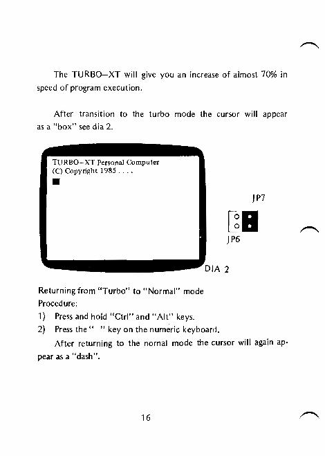
The TURBO-XT will give you an increase of almost 70% in
speed of program execution.
After transition to the turbo mode the cursor will appear
as a "box" see d ia 2.
TURBO-XT Personal Computer (C) Copyright 1985 ....
• JP7
~ JP6
Returning from "Turbo" to "Normal" mode
Procedure:
1) Press and hold "etrl" and" Alt" keys.
2) Press the "-" key on the numeric keyboard.
After returning to the nornal mode the cursor will again ap
pear as a "dash".
16
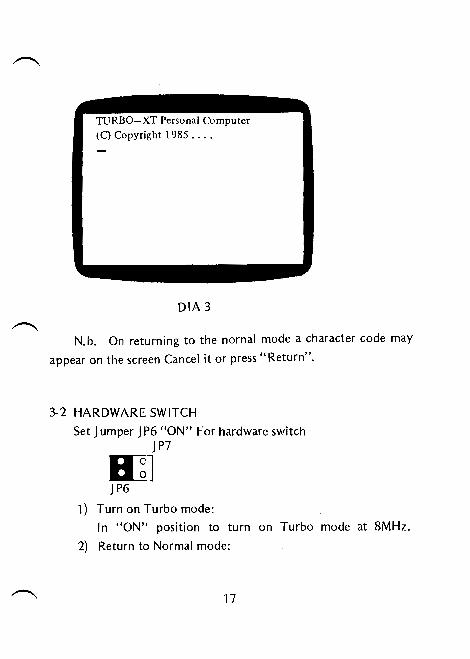
TURBO--XT Personal Computer (C) Copyright 1985 ....
DIA 3
N.b. On returning to the nornal mode a character code may
appear on the screen Cancel it or press "Return".
3-2 HARDWARE SWITCH
Set Jumper JP6 "ON" For hardware switch JP7
~ JP6
1) Turn on Turbo mode:
In "ON" position to turn on Turbo mode at SMHz.
2) Return to Normal mode:
17
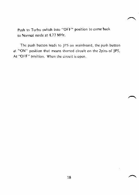
Push to Turbo switch into "OFF" position to come back
to Normal mode at 4.77 MHz.
The push button leads to JPS on main board, the push button
at "ON" position that means shorted circuit on the 2pins of JPS,
At "OFF" position. When the circuit is open.
18
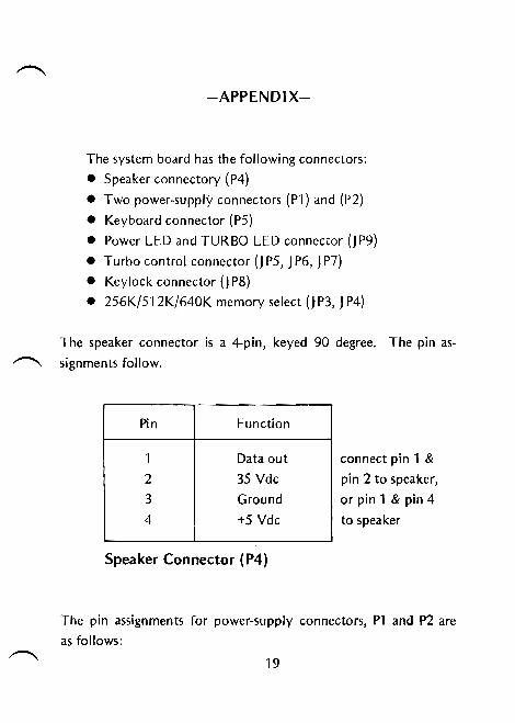
-APPENDIX-
The system board has the following connectors:
• Speaker connectory (P4)
• Two power-supply connectors (Pl) and (P2)
• Keyboard connector (P5)
• Power LED and TURBO LED connector (j P9)
• Turbo control connector (J P5, JP6, JP7)
• Keylock connector (j P8)
• 256K/512K/640K memory select (j P3, JP4)
The speaker connector is a 4-pin, keyed 90 degree. The pin as
~ signments follow.
Pin Function
1 Data out connect pin 1 &
2 35 Vdc pin 2 to speaker,
3 Ground or pin 1 & pin 4
4 +5 Vdc to speaker
Speaker Connector (P4)
The pin assignments for power-supply connectors, Pl and P2 are
as follows:
19
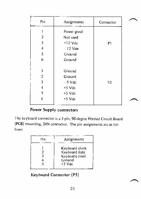
Pin
1
2
3
4
5
6
1
2
3
4
5
6
Assignments
Power good
Not used
+12 Vdc
~12 Vde
Ground
Ground
Ground
Ground
~5 Vdc
+5 Vdc
+5 Vdc
+5 Vdc
Connector
Pl
P2
Power Supply cunnectors
The keyboard connector is a 5-pin, 90-degree Printed Circuit Board
(PCB) mounting, DIN connector. The pin assignments are as fol
lows:
Pin Assignments
1 Keyboard clock 2 Keyboard data 3 Keyboard reset 4 Ground 5 +5 Vdc
Keyboard Connector (P5)
20

The power LED and LED connector is a 4-pin Berg strip. Its pin
assignments follow:
Pin Assignments
1 Turbo LED (1) pin 1 & pin 2 con
2 Tubo LED (2) nector to turbo
3 LED POWER LED pin 3 & pin
4 Ground 4 to power on LE D
Power LED and Keylock Connector (J P9)
The keyplock connector is a 2-pin, keyed, Berg strip. The pin
assignments follow:
Keyboard locked, J P8 is open10 0 Keyboard unlocked, JP8 is shortted
JP8
21