OFTWARE UART EXAMPLES - Silicon Labs · PDF fileUART receiver. C8051F00x and ... Test code is...
34
Rev. 1.1 12/03 Copyright © 2003 by Silicon Laboratories AN115 AN115 S OFTWARE UART E XAMPLES Relevant Devices This application note applies to the following devices: C8051F000, C8051F001, C8051F002, C8051F005, C8051F006, C8051F010, C8051F011, C8051F012, C8051F012, C8051F015, C8051F016, C8051F017, C8051F220, C8051F221, C8051F226, C8051F230, C8051F231, C8051F236. Introduction This application note presents a discussion about software UART implementation on C8051Fxxx devices. Two complete examples are given: a C program using the PCA as the baud rate source, and an assembly program using Timer 0 as the baud rate source. Key Features The two software examples were designed to closely mimic the hardware UART while still pre- serving hardware resources and CPU bandwidth. The following is a list of key features found in both examples: • An interface similar to the hardware UART, with user-level transmit and receive interrupts. • Interrupt or polled mode access support. • Full-duplex communication up to 57.6 kbps using an 18.432 MHz clock source. • State-based, interrupt-driven implementation, requiring minimal CPU overhead. • Minimal hardware usage: - ‘C’ example uses two PCA modules. - Assembly example uses Timer 0 in Mode 3. Implementation Options The essential trade-off to consider when imple- menting a software UART (SW UART) is between hardware usage and speed/efficiency. Designs that utilize more hardware are likely to consume less CPU bandwidth and allow higher bit rates. This trade-off is discussed below. Baud Rate Sources An interrupt must be generated for each bit that is transferred; at a full-duplex 115.2 kbps, that’s an interrupt every 4.3 μs. The method of generating these interrupts (baud rate source) determines to a large extent how much overhead the implementa- tion consumes. Available options include: 8-bit timers, 16-bit timers, and the Programmable Counter Array (PCA). Note that for full-duplex operation, two baud rate sources are required (one each for transmit and receive). The use of 8-bit timers allows one of the 16-bit hardware timers to be used for both transmit and receive baud rate generation. Timer 0 offers this capability in Mode 3. Note that when Timer 0 is in this mode, Timer 1 functionality is reduced; how- ever, Timer 1 may still provide baud rate genera- tion for the hardware UART (HW UART). Using 8-bit timers preserves hardware resources, but does introduce some overhead and latency issues. These issues are discussed in Example 2. An alternative to the above solution is the use of 16-bit auto-reload timers. In this case two of the 16 bit hardware timers are occupied by the SW UART- -one for transmit and one for receive. Any of the available timers will suffice, but the auto-reload feature on Timer 2 and Timer 3 reduces overhead, and eliminates any interrupt latency issues. Addi- tionally, 16-bit timers support a wider range of baud rates.
Transcript of OFTWARE UART EXAMPLES - Silicon Labs · PDF fileUART receiver. C8051F00x and ... Test code is...

Rev. 1.1 12/03 Copyright © 2003 by Silicon Laboratories AN115
AN115
SOFTWARE UART EXAMPLES
Relevant DevicesThis application note applies to the followingdevices:
C8051F000, C8051F001, C8051F002, C8051F005, C8051F006, C8051F010, C8051F011, C8051F012, C8051F012, C8051F015, C8051F016, C8051F017, C8051F220, C8051F221, C8051F226, C8051F230, C8051F231, C8051F236.
IntroductionThis application note presents a discussion aboutsoftware UART implementation on C8051Fxxxdevices. Two complete examples are given: a Cprogram using the PCA as the baud rate source, andan assembly program using Timer 0 as the baudrate source.
Key FeaturesThe two software examples were designed toclosely mimic the hardware UART while still pre-serving hardware resources and CPU bandwidth.The following is a list of key features found in bothexamples:
• An interface similar to the hardware UART, with user-level transmit and receive interrupts.
• Interrupt or polled mode access support.• Full-duplex communication up to 57.6 kbps
using an 18.432 MHz clock source.• State-based, interrupt-driven implementation,
requiring minimal CPU overhead.• Minimal hardware usage:
- ‘C’ example uses two PCA modules.
- Assembly example uses Timer 0 in Mode 3.
Implementation OptionsThe essential trade-off to consider when imple-menting a software UART (SW UART) is betweenhardware usage and speed/efficiency. Designs thatutilize more hardware are likely to consume lessCPU bandwidth and allow higher bit rates. Thistrade-off is discussed below.
Baud Rate SourcesAn interrupt must be generated for each bit that istransferred; at a full-duplex 115.2 kbps, that’s aninterrupt every 4.3 µs. The method of generatingthese interrupts (baud rate source) determines to alarge extent how much overhead the implementa-tion consumes. Available options include: 8-bittimers, 16-bit timers, and the ProgrammableCounter Array (PCA). Note that for full-duplexoperation, two baud rate sources are required (oneeach for transmit and receive).
The use of 8-bit timers allows one of the 16-bithardware timers to be used for both transmit andreceive baud rate generation. Timer 0 offers thiscapability in Mode 3. Note that when Timer 0 is inthis mode, Timer 1 functionality is reduced; how-ever, Timer 1 may still provide baud rate genera-tion for the hardware UART (HW UART). Using8-bit timers preserves hardware resources, but doesintroduce some overhead and latency issues. Theseissues are discussed in Example 2.
An alternative to the above solution is the use of16-bit auto-reload timers. In this case two of the 16bit hardware timers are occupied by the SW UART--one for transmit and one for receive. Any of theavailable timers will suffice, but the auto-reloadfeature on Timer 2 and Timer 3 reduces overhead,and eliminates any interrupt latency issues. Addi-tionally, 16-bit timers support a wider range ofbaud rates.
AN115
2 Rev. 1.1
The Programmable Counter Array (PCA) also pro-vides an excellent solution for the SW UART, asdemonstrated in the provided ‘C’ example. ThePCA consists of a dedicated 16-bit counter/timerand five 16-bit capture/compare modules. Each ofthese modules may be configured to trigger aninterrupt when the PCA counter matches the asso-ciated compare module’s contents. Since the PCAcounter runs uninterrupted, this solution avoids theproblem of accumulated interrupt latency. ThePCA implementation is not available onC8051F2xx devices.
Additional ConsiderationsEach of the above timer sources may be clocked bySYSCLK or an external signal. In the providedexamples, baud rate sources are clocked bySYSCLK, which is derived from an external18.432 MHz crystal. Any baud rate/crystal fre-quency combination is allowed, though softwareoverhead limits the maximum baud rate-to-SYSCLK ratio.
START bit detection is also a concern for the SWUART receiver. C8051F00x and C8051F01xdevices offer many external interrupt sources, sev-eral of which can be configured to detect fallingedges. Both example programs utilize externalinterrupts for START detection.
Example 1: Programmable Counter Array ImplementationExample 1 uses two PCA modules to generate thereceive and transmit baud rates (modules 0 and 1,respectively). The modules are configured in soft-ware timer mode to generate baud rate interrupts.An introduction to the PCA can be found inAN007.
Program StructureIn software timer mode, the PCA can generate aninterrupt when the PCA counter matches a value inof one of the compare modules. Since the PCAcounter runs uninterrupted, the modules can beupdated each bit time to accurately produce thenext bit time. In addition, the PCA offers a capturefunction that is useful in START bit detection.
The PCA modules may be routed via the crossbarto external signals. These signals (called CEXn formodule n) can be used to trigger PCA counter cap-tures. This feature is exploited in the SW UARTreceiver. START bit recognition is accomplishedwith module 0 configured to capture the PCAcounter contents upon a falling edge on the RX pin.This function offers two benefits: (1) START bitdetection is easily accomplished; and (2) since thecapture is performed immediately as the edge isdetected, the bit sample timing is immune to inter-rupt latency.
ImplementationThe transmit and receive operations for Example 1are implemented as two independent state

AN115
Rev. 1.1 3
machines in the PCA ISR. The state machines areillustrated in Figure 1.
Receive State MachineWhen the SW UART is initialized, the PCAmodule 0 is configured for negative-edge capturemode. Its input, CEX0, is routed via the crossbar toa GPIO pin (P0.2, SW_RX). With the statemachine in State 0, an interrupt is generated when afalling edge is detected on SW_RX. Since the mod-ule is in capture mode, the contents of the PCAcounter are loaded into the module 0 capture regis-ters. Note that this value is independent of interruptlatency. Module 0 is switched to software timer
mode after the START bit is detected, and 3/2 bit-time is added to the module 0 capture register. Theextra 1/2 bit-time is used only after the start bit isdetected, so that sampling will occur during themiddle of the next bit period (see Figure 2). Whenthe PCA counter reaches the value held in themodule 0 capture registers, the first bit-samplinginterrupt (LSB in this case) occurs.
States 1-8 execute on module match interrupts. Ineach state, bits are sampled from SW_RX andshifted into the RXSHIFT variable. The PCAmodule 0 contents are updated in each state to pro-vide the next bit-time interrupt (1 bit time is added
Figure 1. Transmit and Receive State Machines
State 0: Transmit START bit.- Drop TX pin as START condition.- Update Baud Rate source for next bit time.- Increment state variable.
State 1-9:Transmit Bit.- Shift LSB of Transmit Data onto TX pin.- Shift STOP bit into MSB of Transmit Data.- Update Baud Rate source for next bit time.- Increment state variable.
State 10: STOP bit transmitted.- Indicate Transmit complete.- Trigger user-level interrupt if enabled.- Reset Transmitter to Idle state.
Transmit State Machine
Interrupt Sources
State 0: Start bit detected.- Load Baud Rate source for 3/2 bit time.- Increment state variable.
State 1-8: Bit Received.- Shift value of RX pin into RX shift register.- Update Baud Rate source for next bit time.- Increment state variable.
State 9: Capture STOP bit.- Indicate Receive complete.- Trigger user-level interrupt if enabled.- Reset Receiver to Idle state.
Receive State Machine
Interrupt Sources
1) User (begin TX)2) Bit Time Generator
1) START detection2) Bit Time Generator
Figure 2. SW UART Bit Timing
D1D0 D2 D3 D4 D5 D6 D7START
BITMARK
STOPBIT
BIT TIMES
BIT SAMPLING
SPACE
3/2 Bit-Time 1 Bit-Time

AN115
4 Rev. 1.1
to the compare registers). The state variable is alsoincremented.
State 9 captures the STOP bit, posts SRI, andreturns the receiver to Idle state.
Transmit State MachineA user initiates a transmit by forcing a PCAmodule 1 interrupt (setting CCF1=1). In State 0,the TX pin is forced low to generate the STARTcondition. The PCA counter is read, and this valueplus one bit-time is loaded into to the module 1capture registers. Note that a few SYSCLKs willpass between the time the START bit is generatedand when the PCA counter is read. This is the onlyinstance in Example 1 where interrupt latencyaffects the bit time. The effect is negligible (worstcase ~ 1/16 bit-time for 57.6 kbps and an18.432 MHz SYSCLK).
States 1-9 are executed on module match inter-rupts. In each state, a bit is shifted out of the LSBof TDR, and a ‘1’ shifted in the MSB of TDR torepresent the STOP bit. One bit time is added to thePCA module 1 capture registers to generate thenext bit time. After 9 shifts, the data byte + STOPbit have been transmitted. The Transmit Completeindicator (STI) is set, the Transmit Busy indicator(STXBSY) is cleared, and the TX state variable isreset.
Program InterfaceThe SW UART supports both polled and interrupt-driven interfacing. Polled support is configured bydisabling user-level interrupts (SES=0). The trans-mit and receive indicators (STI and SRI, respec-tively) can then be polled for transfer completions.The initialization and polled mode programming
procedure for Example 1 is shown in Figure 3.
The initialization routine, SW_UART_INIT, con-figures the PCA, interrupts, and state variables for
1) Read RDR.2) Clear SRI
SRI
1
0
To Receive
STXBSY
1) Write data to TDR.2) Set CCF1 toinitiate transmit.3) Set STXBSY
STI
1
0
0
1
To Transmit
Done?
End RX
No
Yes
Done?NoYes
End TX
Initialization
1) Define SYSCLK and desiredBAUD_RATE.2) Call SW_UART_INIT.3) Set SES if user-level interruptsupport is desired.4) Set SREN to enable the SW UARTreceiver.5) Call SW_UART_ENABLE.
1) Clear STI
Figure 3. Example 1 User-Level Polled Mode Interface
AN115
Rev. 1.1 5
use in the SW UART. The SW_UART_ENABLEroutine enables the SW UART. The SREN bit mustbe set to enable the receiver. Note that theTIME_COUNT constant is calculated by the soft-ware from the BAUD_RATE and SYSCLK con-stants.
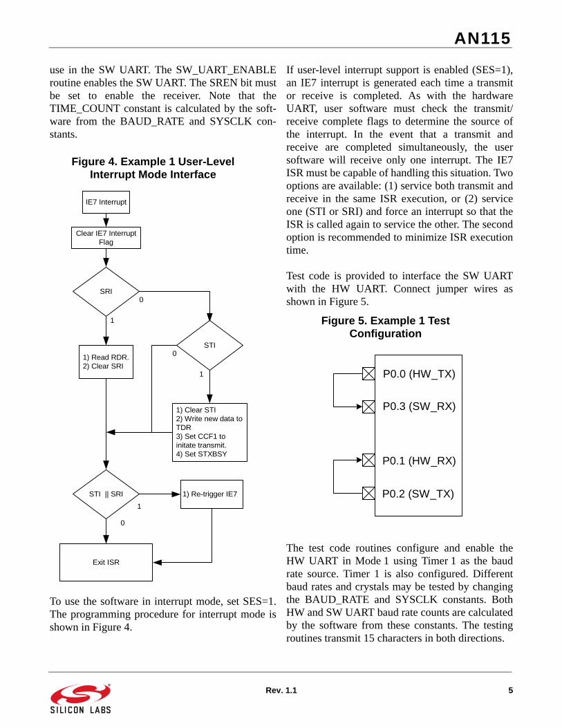
To use the software in interrupt mode, set SES=1.The programming procedure for interrupt mode isshown in Figure 4.
If user-level interrupt support is enabled (SES=1),an IE7 interrupt is generated each time a transmitor receive is completed. As with the hardwareUART, user software must check the transmit/receive complete flags to determine the source ofthe interrupt. In the event that a transmit andreceive are completed simultaneously, the usersoftware will receive only one interrupt. The IE7ISR must be capable of handling this situation. Twooptions are available: (1) service both transmit andreceive in the same ISR execution, or (2) serviceone (STI or SRI) and force an interrupt so that theISR is called again to service the other. The secondoption is recommended to minimize ISR executiontime.
Test code is provided to interface the SW UARTwith the HW UART. Connect jumper wires asshown in Figure 5.
The test code routines configure and enable theHW UART in Mode 1 using Timer 1 as the baudrate source. Timer 1 is also configured. Differentbaud rates and crystals may be tested by changingthe BAUD_RATE and SYSCLK constants. BothHW and SW UART baud rate counts are calculatedby the software from these constants. The testingroutines transmit 15 characters in both directions.
Figure 4. Example 1 User-Level Interrupt Mode Interface
Exit ISR
STI || SRI 1) Re-trigger IE7
1
0
1) Read RDR.2) Clear SRI
SRI
1
0
IE7 Interrupt
STI
1) Clear STI2) Write new data toTDR3) Set CCF1 toinitate transmit.4) Set STXBSY
Clear IE7 InterruptFlag
1
0
Figure 5. Example 1 Test Configuration
P0.0 (HW_TX)
P0.3 (SW_RX)
P0.1 (HW_RX)
P0.2 (SW_TX)

AN115
6 Rev. 1.1
To test the SW UART in polled mode, comment theline
; INTERRUPT_TEST();
and uncomment the line
POLLED_TEST();
Reverse the above steps to test the SW UART ininterrupt mode. Uncomment the line
INTERRUPT_TEST();
And comment the line
; POLLED_TEST();
The longest states in Example 2 require 113SYSCLKs (TX States 1-9). For an 18.432 MHzcrystal, a SW UART transmit or receive operationwill require a worst case 6 µs per bit transferred(113*TSYSCLK). At 57.6 kbps, that’s ~35% of CPUbandwidth for a transmit or receive (70% for full-duplex). For the Example 1 software compiled withthe Keil compiler, the full-duplex overhead may beapproximated by the following equation:
FD Overhead(%) ~ = BAUD_RATE/81,000
Per the above equation, baud rates above 80 kbpsare not supported for full duplex operation. Theoverhead penalty is only incurred while the SWUART is performing a transfer. The code listingbegins on page 10.
Example 2: 8-Bit Timer ImplementationIn Example 1 the SW UART uses Timer 0 inMode 3. In this mode, Timer 0 is split into two 8-bit timers: one is used for transmitting and one forreceiving. TL0 is used as the receive timer; TH0 isused as the transmit timer.
With Timer 0 in Mode 3, Timer 1 may not set theTF1 flag, generate an interrupt, or be clocked byexternal signals. However, Timer 1 may still oper-ate as a baud rate generator for the HW UART ifconfigured in Mode 2 (8-bit timer w/auto-reload).While Timer 0 is in Mode 3, Timer 1 may beenabled/disabled through its mode settings. Timer1 is disabled in Mode 3, and enabled in all othermodes.
With Timer 1 as the HW UART baud rate source,this solution is perhaps the most efficient use ofhardware resources. The downside is increasedsoftware overhead (relative to the 16-bit timer solu-tion). Timer 0 Mode 3 does not offer auto-reloadcapabilities; the manual timer reload requires a 16-bit move in each interrupt service routine (ISR)iteration. In addition, interrupt latency will affectthe bit-time accuracy. A correction constant can befactored into the timer preload values to compen-sate for typical interrupt latency, but variations ininterrupt latency are unaccounted for.
Slower baud rates may require more than 8-bits oftimer counts for each bit time. With SYSCLK at18.432 MHz and Timer 0 in SYSCLK/1 mode,baud rates below 72 kbps require more than 256timer counts. Available options include:
1) Use Timer 0 in SYSCLK/12 mode. Slower baudrates may be achieved with 8 bits, but standardbaud rate/SYSCLK combinations are more difficultto obtain.
2) Use Timer 0 in SYSCLK/1 mode, and keep anupper timer byte manually in the timer ISR. Notethat this method will generate an interrupt every256 SYSCLKs for each transmit and receive,regardless of the baud rate (an interrupt each timethe lower 8-bits overflow). The Example 2 soft-ware demonstrates option #2.
Program StructureThe transmit and receive operations for Example 2are implemented as two independent state
AN115
Rev. 1.1 7
machines in the Timer 0 and Timer 1 ISRs (seeFigure 1 on page 3). The Timer 0 ISR is used tomanage the receive state machine; the Timer 1 ISRmanages the transmit state machine. The /INT0ISR starts the receive state machine, but is disabledwhen the receive state is non-zero.
The SW UART receiver captures the START bitusing an external interrupt source, /INT0, config-ured for active-low edge-sensitive input. The /INT0interrupt is enabled when waiting for a START bit,and disabled during transfers. /INT0 is routed to theGPIO pins via the crossbar. Details on crossbarconfiguration can be found in AN001.
Since all timer loading is performed manually inthe ISR, interrupt latency must be compensated for.A ‘slop constant’ is subtracted from each timer pre-load value to adjust for this interrupt latency andcode executed between the timer overflow and theoperation of reloading the new timer values. Theseconstants are independent of the SYSCLK fre-quency or baud rate; however, they do not accountfor variations in interrupt latency.
Implementation NOTE: For this discussion, assume the baud rate isslow enough that the 8-bit timers are not sufficient.The direct RAM bytes labeled BCRHI and BCTHIare used to manually keep the upper bytes for thereceive and transmit timers, respectively.
Transmit State MachineWhen the SW UART is initialized and enabled, theTX interrupt is set pending but still disabled. Theuser initiates the transfer by enabling the transmitinterrupt (Note that TH0, the upper byte ofTimer 0, generates the TX interrupts).
In State 0, the TX pin is asserted low to produce theSTART condition, and the timer is loaded with 1 bittime to produce the next interrupt.
; Load high byte into BCTHImov BCTHI, #HIGH(TX_BT);; Load low byte into TH0
mov TH0, #-LOW(TX_BT);
Notice that BCTHI is loaded with the unsigned bit-time high byte, but TH0 is loaded with the negativeof the bit-time low byte. This is because Timer 0(as all hardware timers) is an up-counter, whileBCTHI counts down. TH0 will overflow and gen-erate an interrupt as it overflows from 0xFF to0x00; BCTHI is decremented upon each interrupt,and indicates a bit time when it equals zero.
For States 1-9, one state is executed each timeBCTHI reaches zero. In each State, the LSB of theTransmit data register (TDR) is shifted onto the TXpin. The TX timer is loaded with 1 bit time, and a‘1’ is shifted into the MSB of TDR to represent theSTOP bit in State 9 (TDR should hold 0xFF afterthe transfer is complete).
State 10 sets the Transmit Complete indicator(STI), clears the Transmit Busy indicator(STXBSY), and triggers an IE7 interrupt if user-level interrupt support is enabled.
Receive State MachineIn State 0, /INT0 is used as the RX input (config-ured falling-edge active, HIGH priority). An /INT0interrupt means a START condition has beendetected. The /INT0 ISR loads the RX timer (TL0+ BCRHI) with 3/2 bit-time (see Figure 2). BCRHIis decremented each time TL0 overflows.
States 1-8 execute when BCRHI reaches zero. Ineach state, the SW_RX pin is sampled and shiftedinto the LSB of the RXSHIFT variable. The RXtimer is also reloaded to generate the next samplingtime. State 9 captures the STOP bit, but framingerror detection is not provided (the STOP bit polar-ity is not checked). If user-level interrupts areenabled, this state enables and triggers the IE7interrupt.
Program InterfaceExample 2 supports both polled and interruptdriven interfacing. The initialization ritual and pro-gramming procedure for polled mode is shown in

AN115
8 Rev. 1.1
Figure 6. The TIME_COUNT constant must beexplicitly defined in this example.
Figure 6. Example 2 User-Level Polled Mode Interface
Initialization
1) Define TIME_COUNT according todesired baud rate and SYSCLK.2) Call SW_UART_INIT.3) Set SES if user-level interruptsupport is desired.4) Set SREN to enable the SW UARTreceiver.5) Call SW_UART_ENABLE.
1) Read RDR.2) Clear SRI
SRI
1
0
To Receive
STXBSY
1) Write data to TDR.2) Set ETI to initiatetransmit.3) Set STXBSY
STI
1
0
1) Clear STI
0
1
To Transmit
Done?
End RX
End TX Done?NoYes
Yes
No

AN115
Rev. 1.1 9
Figure 7 shows the IE7 ISR programming sequencefor interrupt mode. Note that the receive operationis serviced first, since it is the most sensitive tolatency.
To handle the situation of a transmit and receivecompleting simultaneously, this example services
one function and re-triggers itself to service theother.
Test code is provided. To test the polled mode code,in the MAIN routine uncomment the line
ajmp PolledRX_PolledTX
and comment the line
; ajmp InterruptRX_InterruptTX
To run the interrupt mode test code, reverse theabove steps. Comment the line
; ajmp PolledRX_PolledTX
and uncomment the line
ajmp InterruptRX_InterruptTX
Adding a jumper wire between SW_GPIO_TX andSW_GPIO_RX provides quick and easy evaluationof the SW UART. Note that this evaluation methodis only useful with the interrupt mode test code.
With a SYSCLK of 18.432 MHz, the softwaregiven in Example 2 operates in full-duplex at amaximum of 57.6 kbps. The code listing begins onpage 21.
Figure 7. Example 2 User-Level Interrupt Interface
Exit ISR
STI
1) Re-trigger IE7
1
0
1) Read RDR.2) Clear SRI
SRI
1
0
IE7 Interrupt
STI
1) Clear STI2) Write new data toTDR3) Set ETI to initatetransmit.4) Set STXBSY
SRI
1) Re-trigger IE7
1
0
Clear IE7 Interrupt Flag
0
1
AN115
10 Rev. 1.1
//------------------------------------------------------------------------------------//// Copyright 2003 Cygnal, Inc.//// FILE NAME: AN015_1.c// TARGET DEVICE: C8051F00x, C8051F01x// CREATED ON: 03/10/01// CREATED BY: JS//// Software UART program, using PCA as baud rate source.// PCA module 0 is used as receive baud rate source and START detector. For START// detection, module 0 is configured in negative-edge capture mode. For all other// SW_UART operations, module 0 is configured as a software timer. Module match// interrupts are used to generate the baud rate. Module 1 generates the transmit// baud rate in software timer mode. // Code assumes an external crystal is attached between the XTAL1 and XTAL2 pins.// The frequency of the external crystal should be defined in the SYSCLK constant.// // INITIALIZATION PROCEDURE:// 1) Define SYSCLK according to external crystal frequency.// 2) Define desired BAUD_RATE.// 3) Call SW_UART_INIT().// 4) Set SREN to enable SW_UART receiver.// 5) Set SES only if user-level interrupt support is desired.// 6) Call SW_UART_ENABLE().//// TO TRANSMIT:// 1) Poll STXBSY for zero.// 2) Write data to TDR.// 3) Set CCF1 to initiate transmit.// 4) STI will be set upon transmit completion. An IE7 interrupt is generated if // user-level interrupts are enabled.//// TO RECEIVE:// 1) If in polled mode, poll SRI. If in interrupt mode, check SRI in IE7 Interrupt// Service Routine.// 2) Read data from RDR.// // Test code is included, for both polled and interrupt mode. Test code assumes// the HW_UART pins and SW_UART pins are connected externally:// P0.0 (HW_UART TX) -> P0.3 (SW_UART RX)// P0.1 (HW_UART RX) -> P0.2 (SW_UART TX)// // To use the test code in polled mode, comment out the call to the INTERRUPT_TEST()// at the bottom of the main routine, and uncomment the call to POLLED_TEST(). To // test the interrupt mode, comment out the POLLED_TEST() call and uncomment the// INTERRUPT_TEST() call.//// The test routines configure the HW_UART to operate with Timer 1 as the baud rate// source. The Timer 1 preload values are auto-calculated from the SYSCLK and BAUD_RATE// constants.////-----------------------------------------------------------------------------------// Includes//-----------------------------------------------------------------------------------#include <c8051f000.h> // SFR declarations
//-----------------------------------------------------------------------------------// Global CONSTANTS

AN115
Rev. 1.1 11
//-----------------------------------------------------------------------------------
#define BAUD_RATE 57600 // User-definable SW_UART baud rate#define SYSCLK 18432000 // System clock derived from
// 18.432MHz XTL
#define TIME_COUNT SYSCLK/BAUD_RATE/4 // Number of PCA counts for one // bit-time. (PCA configured to count// SYSCLK/4)
#define TH_TIME_COUNT TIME_COUNT*3/2 // 3/2 bit-time, for use after receiving// a START bit. RX should be LOW for one// bit-time after the edge of the START,// and the first bit sample starts in// the middle of the next bit-time.
#define HW_TIME_COUNT SYSCLK/BAUD_RATE/16 // Time count for HW_UART baud rate// generation. Auto-calculated from the// SYSCLK and BAUD_RATE constants// defined above.
//-----------------------------------------------------------------------------------//Global VARIABLES//-----------------------------------------------------------------------------------
bit SRI; // SW_UART Receive Complete Indicatorbit STI; // SW_UART Transmit Complete Indicatorbit STXBSY; // SW_UART TX Busy flagbit SREN; // SW_UART RX Enablebit SES; // SW_UART User-level Interrupt
// Support Enable
sbit SW_RX = P0^2; // SW_UART Receive pinsbit SW_TX = P0^3; // SW_UART Transmit pin
char TDR; // SW_UART TX Data Registerchar RDR; // SW_UART RX Data Register (latch)
// Test Variableschar k, m; // Test indices.char idata SW_BUF[20]; // SW_UART test receive buffer.
bit HW_DONE; // HW transfer complete flag // (15 characters transmitted.)
bit SW_DONE; // SW transfer complete flag // (15 characters transmitted.)
//------------------------------------------------------------------------------------// Function PROTOTYPES//------------------------------------------------------------------------------------
void SW_UART_INIT(); // SW_UART initialization routinevoid SW_UART_ENABLE(); // SW_UART enable routinevoid PCA_ISR(); // SW_UART interrupt service routinevoid INTERRUPT_TEST(void); // SW_UART test routine (interrupt mode)void POLLED_TEST(void); // SW_UART test routine (polled mode)void USER_ISR(void); // SW_UART test interrupt service
// routinevoid HW_UART_INIT(void); // HW_UART initialization and setup
AN115
12 Rev. 1.1
// routinevoid HW_UART_ISR(void); // HW_UART interrupt service routine
//------------------------------------------------------------------------------------// MAIN Routine//------------------------------------------------------------------------------------// - Disables Watchdog Timer// - Configures external crystal; switches SYSCLK to external crystal when stable.// - Configures crossbar and ports.// - Initializes and enables SW_UART.// - Calls Test Routines.//void MAIN (void){
int delay; // Delay counter.
OSCXCN = 0x66; // Enable external crystalWDTCN = 0xDE; // disable watchdog timerWDTCN = 0xAD;
// Port SetupXBR0 = 0x0C; // HW_UART routed to pins P0.0 and P0.1;
// CEX0 routed to pin P0.2.XBR2 = 0x40; // Enable crossbar, pull-ups enabled.
PRT0CF = 0x09; // P0.0 (HW TX), and P0.3 (SW TX)// configured for push-pull output.
delay=256; // Delay >1 ms before polling XTLVLD.while(delay--);
while (!(OSCXCN & 0x80)); // Wait until external crystal has// started.
OSCICN = 0x0C; // Switch to external oscillatorOSCICN = 0x88; // Disable internal oscillator; enable
// missing clock detector.
POLLED_TEST(); // Call Polled mode SW_UART test // routine.
// INTERRUPT_TEST(); // Call Interrupt mode SW_UART test // routine.
while(1); // Spin forever}
//------------------------------------------------------------------------------------// Functions//------------------------------------------------------------------------------------
//------------------------------------------------------------------------------------// INTERRUPT_TEST: SW_UART Interrupt Mode Test// Test code to transmit and receive 15 characters to/from the HW_UART (in interrupt// mode), with SW_UART in interrupt mode.// - Initializes and enables the SW_UART & HW_UART// - Clears all test variables & counters// - Transfers 15 characters from HW to SW_UART, and 15 characters from SW to HW_UART,// simultaneously. //void INTERRUPT_TEST(void){

AN115
Rev. 1.1 13
SW_UART_INIT(); // Initialize SW_UARTSW_UART_ENABLE(); // Enable SW_UARTSREN = 1; // Enable SW_UART ReceiverSES = 1; // User-level interrupt support enabled.
HW_UART_INIT(); // Configure HW_UART for testing // routine.
k=m=0; // Clear user ISR counters.
HW_DONE=0; // Clear transfer complete indicatorsSW_DONE=0; //
IE |= 0x10; // Enable HW_UART interruptsSTI = 1; // Indicate transmit complete to
// initiate first transfer.
EIE2 |= 0x20; // Start SW_TX by enablingPRT1IF |= 0x80; // and forcing an IE7 interrupt
TI = 1; // Initiate a HW_UART transmit // by forcing TX interrupt.
while(!(HW_DONE&SW_DONE)); // Wait for transfers to finish.}
//------------------------------------------------------------------------------------// POLLED_TEST: SW_UART Polled Mode Test// Test code to transmit and receive 15 characters to/from the HW_UART, with SW_UART// in polled mode.// - Initializes and enables the SW_UART & HW_UART// - Clears all test variables & counters// - Sends 15 characters from the HW_UART to be received by SW_UART.// - Sends 15 characters from the SW_UART to be received by the HW_UART.//void POLLED_TEST(void){
SW_UART_INIT(); // Initialize SW_UARTSW_UART_ENABLE(); // Enable SW_UARTSREN = 1; // Enable SW_UART ReceiverSES = 0; // Disable user-level interrupt support.
HW_UART_INIT(); // Configure HW_UART for testing // routine.
k=m=0; // Clear test counter variables.HW_DONE = 0; // Clear transfer complete indicatorsSW_DONE = 0; //IE |= 0x10; // Enable HW_UART interrupts.
TI = 1; // Initiate a HW_UART transmit // by forcing TX interrupt.
// Receive 15 characters with SW_UART; transmit with HW_UART.while(SREN){ // Run while SW_UART Receiver
// is enabled.if (SRI){ // If Receive Complete:
SR = 0; // Clear receive flag.SW_BUF[k++] = RDR; // Read receive buffer.if (k==15) // If 15 characters have been received:
SREN = 0; // Disable SW_UART Receiver.

AN115
14 Rev. 1.1
} // Indicate 15 characters received}
// Transmit 15 characters with SW_UART; receive with HW_UART.while(STXBSY); // Poll Busy flag.STXBSY = 1; // Claim SW_UART TransmitterTDR=m++; // Load TX data.CCF1=1; // Initiate first SW_UART TX
// by forcing a PCA module 1 interrupt.
while(!SW_DONE){ // SW_UART transmitting here// HW_UART receiving.
if (STI){ // If Transmit Complete:STI = 0; // Clear transmit flag.if (m<16){ // Transmit 15 characters.
STXBSY = 1; // Claim SW_UART TransmitterTDR = m++; // Transmit, increment variable.CCF1 = 1; // Force module 1 interrupt to
} // initiate TX.else // If this is 15th character,
SW_DONE=1; // Indicate last character transmitted.}
}}
//------------------------------------------------------------------------------------// HW_UART_INIT: HW_UART Initialization Routine// Sets up HW_UART for use in SW_UART testing.// - HW_UART in Mode 1// - Timer 1 used as baud rate source, clocked by SYSCLK.//void HW_UART_INIT(void) {
PCON |= 0x80; // SMOD=1 (HW_UART uses Timer 1 overflow// with no divide down).
TMOD = 0x20; // Configure Timer 1 for use by HW_UARTCKCON |= 0x10; // Timer 1 derived from SYSCLKTH1 = -HW_TIME_COUNT; // Timer 1 initial valueTL1 = -HW_TIME_COUNT; // Timer 1 reload value
TR1 = 1; // Start Timer 1
RI=0; // Clear HW_UART receive and transmitTI=0; // complete indicators.
SCON = 0x50; // Configure HW_UART for Mode 1,// receiver enabled.
}//------------------------------------------------------------------------------------// SW_UART_INIT: SW_UART initialization routine// Prepares SW_UART for use.// - Configures PCA: Module 0 in negative capture mode; module 1 in software // timer mode; PCA time base = SYSCLK/4; PCA interrupt disabled; PCA counter// disabled.// - Clears pending PCA module 0 and 1 interrupts// - Resets TX and RX state variables//

AN115
Rev. 1.1 15
void SW_UART_INIT(void){
PCA0CPM0 = 0x10; // Module 0 in negative capture mode; // module 0 interrupt disabled.
PCA0CPM1 = 0x48; // Module 1 in software timer mode; // module 1 interrupt disabled.
PCA0CN = 0; // Leave PCA disabledPCA0MD = 0x02; // PCA timebase = SYSCLK/4; PCA counter
// interrupt disabled.
CCF0 = 0; // Clear pending PCA module 0 andCCF1 = 0; // module 1 capture/compare interrupts.
SRI = 0; // Clear Receive complete flag.STI = 0; // Clear Transmit complete flag.
SW_TX = 1; // TX line initially high.STXBSY = 0; // Clear SW_UART Busy flag
}
//------------------------------------------------------------------------------------// SW_UART_ENABLE: SW_UART Enable Routine// Enables SW_UART for use.// - Enables PCA module 0 interrupts// - Enables PCA module 1 interrupts// - Starts PCA counter.//void SW_UART_ENABLE(void){
PCA0CPM0 |= 0x01; // Enable module 0 (receive) interrupts.PCA0CPM1 |= 0x01; // Enable module 1 (transmit)
// interrupts.
CR = 1; // Start PCA counter.EIE1 |= 0x08; // Enable PCA interruptsEA = 1; // Globally enable interrupts
}
//------------------------------------------------------------------------------------// Interrupt Service Routines//------------------------------------------------------------------------------------//// PCA_ISR: PCA Interrupt Service Routine.// This ISR is triggered by both transmit and receive functions, for each bit that// is transmitted or received. // - Checks module 0 interrupt flag (CCF0); if set, services receive state.// - Checks module 1 interrupt flag (CCF1); if set, services transmit state.//void PCA_ISR(void) interrupt 9 {
static char SUTXST = 0; // SW_UART TX state variablestatic char SURXST = 0; // SW_UART RX state variablestatic unsigned char RXSHIFT; // SW_UART RX Shift Register
unsigned int PCA_TEMP; // Temporary storage variable for
AN115
16 Rev. 1.1
// manipulating PCA module // high & low bytes.
// Check receive interrupt flag first; service if CCF0 is set.if (CCF0){
CCF0 = 0; // Clear interrupt flag.switch (SURXST){
// State 0: START bit received.// In this state, a negative edge on SW_TX has caused the interrupt,// meaning a START has been detected and the PCA0CP0 registers have // captured the value of PCA0.// - Check for receive enable and good START bit// - Switch PCA module 0 to software timer mode// - Add 3/2 bit time to module 0 capture registers to sample LSB.// - Increment RX state variable.case 0:
if (SREN & ~SW_RX){ // Check for receive enable and a good// START bit.
PCA_TEMP = (PCA0CPH0 << 8); // Read module 0 contents intoPCA_TEMP |= PCA0CPL0; // PCA_TEMP.
PCA_TEMP += TH_TIME_COUNT; // Add 3/2 bit times to PCA_TEMP
PCA0CPL0 = PCA_TEMP; // Restore PCA0CPL0 and PCA0CPH0PCA0CPH0 = (PCA_TEMP >> 8); // with the updated value
PCA0CPM0 = 0x49; // Change module 0 to software// timer mode, interrupts enabled.
SURXST++; // Update RX state variable.}break;
// States 1-8: Bit Received// - Sample SW_RX pin// - Shift new bit into RXSHIFT// - Add 1 bit time to module 0 capture registers// - Increment RX state variablecase 1:case 2:case 3:case 4:case 5:case 6:case 7:case 8:
RXSHIFT = RXSHIFT >> 1; // Shift right 1 bitif (SW_RX) // If SW_RX=1,
RXSHIFT |= 0x80; // shift '1' into RXSHIFT MSB
PCA_TEMP = (PCA0CPH0 << 8); // Read module 0 contents intoPCA_TEMP |= PCA0CPL0; // PCA_TEMP.
PCA_TEMP += TIME_COUNT; // Add 1 bit time to PCA_TEMP
PCA0CPL0 = PCA_TEMP; // Restore PCA0CPL0 and PCA0CPH0
AN115
Rev. 1.1 17
PCA0CPH0 = (PCA_TEMP >> 8); // with the updated value
SURXST++; // Update RX state variable.break;
// State 9: 8-bits received, Capture STOP bit.// - Move RXSHIFT into RDR.// - Set SRI (indicate receive complete).// - Prepare module 0 for next transfer.// - Reset RX state variable.// - Trigger IE7 if user-level interrupt support is enabled.case 9:
RDR = RXSHIFT; // Move received data to receive // register.
SRI = 1; // Set receive complete indicator.
PCA0CPM0 = 0x11; // Switch module 0 to negative capture// mode; interrupt enabled for START// detection.
SURXST = 0; // Reset RX state variable.
if (SES){ // If user-level interrupt support// enabled
EIE2 |= 0x20; // Enable IE7.PRT1IF |= 0x80; // Trigger IE7.
}break;
}}
// Check Transmit interrupt; service if CCF1 is set.else if (CCF1){
CCF1 = 0; // Clear interrupt flagswitch (SUTXST){
// State 0: Transmit Initiated.// Here, the user has loaded a byte to transmit into TDR, and set the// module 1 interrupt to initiate the transfer.// - Transmit START bit (drop SW_TX)// - Read PCA0, add one bit time, & store in module 1 capture registers// for first bit.// - Increment TX state variable.case 0:
SW_TX = 0; // Drop TX pin as START bit.
PCA_TEMP = PCA0L; // Read PCA counter value intoPCA_TEMP |= (PCA0H << 8); // PCA_TEMP.
PCA_TEMP += TIME_COUNT; // Add 1 bit time.
PCA0CPL1 = PCA_TEMP; // Store updated match value intoPCA0CPH1 = (PCA_TEMP >> 8); // module 1 capture/compare registers.
PCA0CPM1 |= 0x48; // Enable module 1 software timer.

AN115
18 Rev. 1.1
SUTXST++; // Update TX state variable.break;
// States 1-9: Transmit Bit.// - Output LSB of TDR onto TX// - Shift TDR 1 bit right.// - Shift a '1' into MSB of TDR for STOP bit in State 9.// - Add 1 bit time to module 1 capture registercase 1:case 2:case 3:case 4:case 5:case 6:case 7:case 8:case 9:
SW_TX = (TDR & 0x01); // Output LSB of TDR onto SW_TX pin.TDR >>= 1; // Shift TDR right 1 bit.TDR |= 0x80; // Shift '1' into MSB of TDR for
// STOP bit in State 9.
PCA_TEMP = (PCA0CPH1 << 8); // Read module 1 contents intoPCA_TEMP |= PCA0CPL1; // PCA_TEMP.
PCA_TEMP += TIME_COUNT; // Add 1 bit time to PCA_TEMP
PCA0CPL1 = PCA_TEMP; // Restore PCA0CPL1 and PCA0CPH1PCA0CPH1 = (PCA_TEMP >> 8); // with the updated value
SUTXST++; // Update TX state variable.break;
// State 10: Last bit has been transmitted. Transmit STOP bit// and end transfer. // - Transmit STOP bit// - Set TX Complete indicator, clear Busy flag// - Reset TX state// - Prepare module 1 for next transfer.// - Trigger IE7 interrupt if user-level interrupts enabled.case 10:
STI = 1; // Indicate TX complete.SUTXST = 0; // Reset TX state.SW_TX = 1; // SW_TX should remain high.
PCA0CPM1 = 0x01; // Disable module 1 software timer;// leave interrupt enabled for next// transmit.
if (SES){ // If user-level interrupt support// enabled:
EIE2 |= 0x20; // Enable IE7.PRT1IF |= 0x80; // Trigger IE7.
}STXBSY = 0; // SW_UART TX free.break;
}

AN115
Rev. 1.1 19
}}
//------------------------------------------------------------------------------------// USER_ISR: User SW_UART Interrupt Service Routine (IE7 ISR)// If interrupt-mode test code is enabled, this ISR// transmits 15 characters and receives 15 characters. This routine is triggered each// time a SW_UART transmit or receive is completed.// - Checks receive complete indicator, and services.// - Checks transmit complete indicator, and services.// - Checks for transmits or receives that completed during the ISR; if so, triggers the// interrupt again.//void USER_ISR(void) interrupt 19 { // IE7 Interrupt Service Routine
PRT1IF &= ~(0x80); // Clear IE7 interrupt flag
if (SRI){ // If Receive Complete:SRI = 0; // Clear receive flag.SW_BUF[k++] = RDR; // Read receive buffer.if (k==15){ // If 15 characters have been received:
SREN=0; // Disable SW_UART Receiver.} // Indicate 15 characters received.
}
else if (STI){ // If Transmit Complete:STI = 0; // Clear transmit flag.
if (m<15){ // If less than 15 characters:STXBSY = 1; // Claim SW_UART Transmitter.
TDR = m++; // Increment variable, transmit. CCF1 = 1; // Force module 1 interrupt to initiate
} // TX
else SW_DONE=1; // Indicate last character transmitted.
}if (STI|SRI) // If SRI or STI is set, re-trigger
PRT1IF |= 0x80; // interrupt to service.}
//------------------------------------------------------------------------------------// HW_UART_ISR: Hardware UART Interrupt Service Routine// Transmits characters from 1 to 15, and receives 15 characters.// - Checks receive interrupt, and services.// - Checks transmit interrupt, and services.//void HW_UART_ISR(void) interrupt 4 {
static char i=0; // Transmit data variable.static char j=0; // Receive data index.static idata char HW_BUF[20]; // Receive data buffer.
if (RI){ // If Receive Complete:
RI=0; // Clear receive flagHW_BUF[j++] = SBUF; // Read receive bufferif (j==15) // If 15 characters received:
REN=0; // Disable HW_UART receiver.
AN115
20 Rev. 1.1
}
else if (TI){ // If Transmit Complete:
TI = 0; // Clear transmit flagif (i<15) // If characters left to transmit:
SBUF=i++; // Increment variable, transmit.else // If 15 characters transmitted,
HW_DONE=1; // Indicate HW TX finished.
}}
// End of Example 1, Software UART with PCA
AN115
Rev. 1.1 21
;-----------------------------------------------------------------------------; Cygnal, INC.;;; FILE NAME : AN015_2.ASM ; TARGET MCU : C8051F0xx; DESCRIPTION : Example source code for a software UART;; IMPLEMENTATION NOTES:; - uses Timer0 in Mode3 (two 8-bit timers); - Timer0 run/overflow is used for RX state machine; - Timer1 overflow is used for TX state machine; - 8N1, no Framing error detection; - uses IE7 as user-level interrupt; - uses single-byte PC offset for state table implementation; - uses /INT0 falling as START bit detect (primitive START bit verification);;-----------------------------------------------------------------------------
;-----------------------------------------------------------------------------; EQUATES;-----------------------------------------------------------------------------
$MOD8F000
; SW UART constantsSW_TX_GPIO EQU P0.4 ; SW UART TX GPIO pin (can be any GPIO pin)SW_RX_GPIO EQU P0.2 ; SW UART RX GPIO pin (must be /INT0)
TIME_COUNT EQU 320; Note: 320 is the limit for reliable; FD operation...; FOR SYSCLK = 18.432 MHz:; 115200 = 160; 57600 = 320; 38400 = 480; 19200 = 960; 9600 = 1920; 4800 = 3840; 2400 = 7680
TX_CORR EQU 41 ; (41) Timer preload correction value in ; cycles for TX
RX_CORR EQU 47 ; (47) Timer preload correction value in ; cycles for RX
THALF_CORR EQU 113 ; (113)Timer preload correction value for ; 3/2 RX
TX_BT EQU TIME_COUNT - TX_CORR; actual 16-bit bit counter cycle value ; TX
RX_BT EQU TIME_COUNT - RX_CORR; actual 16-bit bit counter cycle value ; RX
THALF_BT EQU TIME_COUNT*3/2 - THALF_CORR ; actual 16-bit 1.5 bit cycle value ; RX
RX_BUFSIZE EQU 16 ; size of RX buffer in chars;-----------------------------------------------------------------------------; VARIABLES;-----------------------------------------------------------------------------

AN115
22 Rev. 1.1
BSEGorg 0h
SRI: DBIT 1 ; SW UART Receive complete flagSTI: DBIT 1 ; SW UART Transmit complete flagSTXBSY: DBIT 1 ; SW UART TX BSY flagSREN: DBIT 1 ; SW UART RX EnableSES: DBIT 1 ; SW UART user-Interrupt Support Enable
DSEG at 30h
TDR: DS 1 ; SW UART TX data registerRDR: DS 1 ; SW UART RX data registerRXSHIFT: DS 1 ; SW UART RX shift registerSURXST: DS 1 ; SW UART RX state variableSUTXST: DS 1 ; SW UART TX state variableBCRHI: DS 1 ; MSB of 16-bit bit timer for SW UART RXBCTHI: DS 1 ; MSB of 16-bit bit timer for SW UART TX
;test variablesRX_TAIL: DS 1 ; write pointer to RX message bufferTX_VAL: DS 1 ; value to transmit;-------------------; Indirect address space variables
ISEG at 80h
RX_BUF: DS RX_BUFSIZE ; RX message buffer
;-------------------; STACK
STACK_TOP: DS 1 ; placeholder in symbol table for ; beginning of hardware stack
;-----------------------------------------------------------------------------; MACRO DEFINITIONS;-----------------------------------------------------------------------------
;-----------------------------------------------------------------------------; RESET AND INTERRUPT VECTOR TABLE;-----------------------------------------------------------------------------
CSEGorg 00hljmp Reset ; RESET initialization vector
org 03hljmp INT0_ISR ; Software UART RX START bit detect
org 0bhljmp Timer0_ISR ; Software UART RX state machine interrupt
org 1bhljmp Timer1_ISR ; Software UART TX state machine interrupt
org 9bhljmp IE7_ISR ; user-level Software UART interrupt

AN115
Rev. 1.1 23
;-----------------------------------------------------------------------------; MAIN PROGRAM CODE;-----------------------------------------------------------------------------
org 0B3h
Main:ajmp PolledRX_PolledTX ; leave one of these lines uncommented
; ajmp InterruptRX_InterruptTX; leave one of these lines uncommented
sjmp $ ; spin forever...
;-----------------------------------------------------------------------------; MAIN SUBROUTINES;-----------------------------------------------------------------------------
;-----------------------------------------------------------------------------; PolledRX_PolledTX;-----------------------------------------------------------------------------; This routine demonstrates polled access to the SW UART.;; The transmitter transmits a sequence from $00 to $ff;; The receiver receives characters and stores them in a circular buffer.;PolledRX_PolledTX:
acall SW_UART_Init ; initialize SW UART (leave in a; disabled state)
setb SREN ; enable SW UART receiverclr SES ; disable user-level interrupt
; supportacall SW_UART_Enable ; enable SW UART
; transmit message -- polled modejb STXBSY, $ ; wait for SW TX available
; transmit chars $00 to $ffclr a
TX_LOOP: setb STXBSY ; claim SW UART Transmittermov TDR, a ; write char to transmit data regsetb ET1 ; initiate SW TX operationinc a ; set next value to writejnb STI, $ ; wait for TX completeclr STI ; clear TX complete indicatorjnz TX_LOOP
TX_LOOP_END:mov RX_TAIL, #RX_BUF ; initialize TAIL pointer
; receive message -- polled modeRX_LOOP: mov r0, RX_TAIL ; indirect address to write character to
jnb SRI, $ ; wait for RX characterclr SRI ; clear RX complete indicatormov @r0, RDR ; store itinc RX_TAIL ; advance TAIL pointermov a, RX_TAIL ; handle TAIL wrappingadd a, #-(RX_BUF + RX_BUFSIZE)
AN115
24 Rev. 1.1
jnc RX_LOOPmov RX_TAIL, #RX_BUF ; wrap TAIL
sjmp RX_LOOP ; repeat forever...
;-----------------------------------------------------------------------------; InterruptRX_InterruptTX;-----------------------------------------------------------------------------; This routine demonstrates interrupt access to the SW UART.;; The receiver receives characters and stores them in a circular buffer.; Both the transmit and receive routines are located in the IE7_ISR handler.;InterruptRX_InterruptTX:
acall SW_UART_Init ; initialize SW UART (leave in a; disabled state)
setb SES ; Enable user-level interrupt supportsetb SREN ; Enable SW UART receiver
mov RX_TAIL, #RX_BUF ; initialize TAIL pointer
acall SW_UART_Enable ; enable SW UART
setb STI ; kick-start SW UART transmitterorl EIE2, #00100000b ; by enabling IE7orl PRT1IF, #10000000b ; and activating IE7
sjmp $
;-----------------------------------------------------------------------------; INTERRUPT VECTORS;-----------------------------------------------------------------------------;-----------------------------------------------------------------------------; Reset Interrupt Vector;; This routine initializes the device and all peripherals and variables.; - External oscillator started (SYSCLK will be switched to external osc. ; once XTLVLD goes high); - Watchdog timer is disabled; - Crossbar and GPIO output modes are defined; - H/W stack pointer is initialized; - interrupt priorities and enables are initialized here; - /INT0; - Timer0; - Timer1
Reset:
mov OSCXCN, #01100110b ; Enable Crystal osc., divide by 1 mode; XFCN = '110' for 18.432 MHz crystal; External oscillator will be selected; below after XTLVLD has gone high; indicating that the external osc; has started and settled (several; hundred microseconds from now).
mov WDTCN, #0deh ; disable watchdog timermov WDTCN, #0adh

AN115
Rev. 1.1 25
; set up Crossbar and Port I/Omov XBR0, #00000100b ; enable HW UART on P0.0 (TX), P0.1 (RX)mov XBR1, #10000100b ; enable /INT0 on P0.2; /SYSCLK on P0.3mov XBR2, #01000000b ; enable crossbar w/ pull-ups enabledorl PRT0CF, #00011101b ; enable P0.0, 0.2, 0.3, and 0.4 as push-pull
; P0.4 is SW UART TX pin; P0.2 is SW UART RX pin
orl PRT1CF, #01000000b ; enable P1.6 (LED on target board) as ; push-pull
mov SP, #STACK_TOP ; init stack pointer to end of allocated RAM
; Wait >1 ms before checking external crystal for stabilityclr amov r0, a ; Clear r0
djnz r0, $ ; Delay ~380 µsdjnz r0, $ ; Delay ~380 µsdjnz r0, $ ; Delay ~380 µs
OSC_WAIT:mov a, OSCXCN ; spin here until crystal osc is stablejnb acc.7, OSC_WAIT
orl OSCICN, #00001000b ; Select external osc. as; system clock source
anl OSCICN, #NOT(00000100b); Disable internal oscillatororl OSCICN, #10000000b ; Enable missing clock detector
; this must be done AFTER; selecting external osc as system; clock source
setb EA ; enable GLOBAL interrupts
ljmp Main
;-----------------------------------------------------------------------------; Timer0_ISR / INT0_ISR;; These interrupts start and drive the SW UART receive state machine;SWRX_STATE_TABLE: ; each table entry is 1 byte
DB SWRX_S0 - SWRX_STATE_TABLE ; IDLE / START detectDB SWRX_S1 - SWRX_STATE_TABLE ; b0DB SWRX_S2 - SWRX_STATE_TABLE ; b1DB SWRX_S3 - SWRX_STATE_TABLE ; b2DB SWRX_S4 - SWRX_STATE_TABLE ; b3DB SWRX_S5 - SWRX_STATE_TABLE ; b4DB SWRX_S6 - SWRX_STATE_TABLE ; b5DB SWRX_S7 - SWRX_STATE_TABLE ; b6DB SWRX_S8 - SWRX_STATE_TABLE ; b7DB SWRX_S9 - SWRX_STATE_TABLE ; STOP bit capture
INT0_ISR:Timer0_ISR:
push PSW ; resource preservationpush acc

AN115
26 Rev. 1.1
mov a, BCRHI ; if BCRHI is non-zero, we need to roll ; through the timer again...
jz SWRX_PROCESS_STATEdec BCRHIajmp Timer0_ISR_EXIT
SWRX_PROCESS_STATE:push DPH ; resource preservationpush DPL
mov a, SURXST ; read state offset from tablemov DPTR, #SWRX_STATE_TABLEmovc a, @A+DPTR ; 'a' now contains state offset (PC)jmp @A+DPTR ; execute state
Timer0_ISR_END: ; ALL RX states return here
pop DPL ; resource restorationpop DPH
Timer0_ISR_EXIT:pop acc ; resource restorationpop PSWreti
;SWRX_S0: RX IDLE state; At this point, a falling edge has been detected on /INT0. ; We first check to see if the SW UART receiver is enabled. If it is, we check; once to see if the RX pin is still low (START bit valid). If it is, we set up ; Timer0 to count for 3/2 bit time in order to capture the LSB. Here, we also ; disable /INT0 interrupts.; - Check for SREN = '1': IF '1':; - Load TL0 with 3/2 bit time value; - Start Timer; - Enable TF0 interrupt; - Disable /INT0 interrupt; - INC state variable to S1; - IF SREN = '0' (SW UART RX disabled); - exit gracefully, next state is S0;SWRX_S0:
jnb SREN, SWRX_S0_END ; Check to see if SW UART RX is enabled; if not, exit and remain at IDLE state
jb SW_RX_GPIO, SWRX_S0_END; check to see if START bit is good
clr EX0 ; disable /INT0
clr TR0 ; Stop Timer0 (low)clr TF0 ; Clear any pending interrupts
mov BCRHI, #HIGH(THALF_BT); set Timer0 (low) + BCRHI for 1.5 bit mov TL0, #-LOW(THALF_BT); times from now (we assume the start
; bit is good)
setb ET0 ; enable Timer0 interruptssetb TR0 ; Start Timer0L
inc SURXST ; next state is SWRX_S1 (we assume START bit ; is good)

AN115
Rev. 1.1 27
SWRX_S0_END:ajmp Timer0_ISR_END
;SWRX_S1 thru SWRX_S8: Capture b0..b7; At this point, we've determined that the START bit is valid, and we're going to ; query RX_GPIO at bit intervals, shifting the results into RXSHIFT.; - If BCRHI is non-zero, then we need to spin through the timer again; - DEC BCRHI; - let timer roll over on its own; - leave state as is; - If BCRHI is zero:; - stop timer; - Move RX_GPIO state into Carry; - Right shift Carry into RXSHIFT ; - set up timer to capture the next bit; - enable timer; - advance state variable;SWRX_S1:SWRX_S2:SWRX_S3:SWRX_S4:SWRX_S5:SWRX_S6:SWRX_S7:SWRX_S8:
clr TR0 ; Stop Timer0 (low)clr TF0 ; Clear any pending interrupts
mov BCRHI, #HIGH(RX_BT) ; load bit time value into 16-bit virtual ; counter
mov TL0, #-LOW(RX_BT)
setb TR0 ; START RX bit timer
mov C, SW_RX_GPIO ; Move RX state into Carry prior to rshift
mov a, RXSHIFTrrc a ; right shift Carry into shift registermov RXSHIFT, a ; re-store
inc SURXST ; advance state variable
SWRX_S2_END:ajmp Timer0_ISR_END
;SWRX_S9: Capture STOP bit; At this point, we've shifted all the data bits into RXSHIFT, and we're ready to ; sample the STOP bit. Here, we indicate that we've received a character, and reset ; the state machine back to IDLE. In this implementation, we don't actually capture ; the STOP bit; we assume it's good. Here's where we would add support for Framing ; Error detection.; - If BCRHI is non-zero, then we need to spin through the timer again; - DEC BCRHI; - let timer roll over on its own; - leave state as is; - If BCRHI is zero:; - stop timer

AN115
28 Rev. 1.1
; - Move RXSHIFT into RDR; - Set SRI; - Disable timer interrupt; - Enable /INT0 interrupt; - Reset state variable to IDLE; - Check to see if User-level interrupt support is enabled (EIS): If so:; - Enable IE7; - Toggle P1.7 to activate IE7;SWRX_S9:
clr TR0 ; Stop Timer0Lmov RDR, RXSHIFT ; move data from shift reg to data reg
setb SRI ; set SW UART SRI bit to indicate RX completeclr ET0 ; Disable Timer0L interruptclr IE0 ; Disable pending /INT0 interruptssetb EX0 ; Enable /INT0 interruptmov SURXST, #00 ; reset RX state to IDLE
jnb SES, SWRX_S9_END ; check to see if user-level interrupt ; support is enabled
orl EIE2, #00100000b ; enable IE7; leave priority aloneorl PRT1IF, #10000000b ; activate IE7
SWRX_S9_END:ajmp Timer0_ISR_END
;-----------------------------------------------------------------------------; Timer1_ISR (note that this is actually called by the upper-half of Timer0; which is operating in Mode 3);; This interrupt drives the SW UART transmit state machine;
SWTX_STATE_TABLE: ; each table entry is 1 byte; 11 entries; total
DB SWTX_S0 - SWTX_STATE_TABLE; START bitDB SWTX_S1 - SWTX_STATE_TABLE; b0DB SWTX_S2 - SWTX_STATE_TABLE; b1DB SWTX_S3 - SWTX_STATE_TABLE; b2DB SWTX_S4 - SWTX_STATE_TABLE; b3DB SWTX_S5 - SWTX_STATE_TABLE; b4DB SWTX_S6 - SWTX_STATE_TABLE; b5DB SWTX_S7 - SWTX_STATE_TABLE; b6DB SWTX_S8 - SWTX_STATE_TABLE; b7DB SWTX_S9 - SWTX_STATE_TABLE; STOP bit onset edgeDB SWTX_S10 - SWTX_STATE_TABLE; STOP bit terminus
Timer1_ISR:push PSW ; resource preservationpush acc
mov a, BCTHI ; if BCTHI is non-zero, we need to roll ; through the timer again...
jz SWTX_PROCESS_STATEdec BCTHIajmp Timer1_ISR_EXIT
SWTX_PROCESS_STATE:push DPH ; resource preservation

AN115
Rev. 1.1 29
push DPL
mov a, SUTXST ; read state offset from tablemov DPTR, #SWTX_STATE_TABLEmovc a, @A+DPTR ; acc now contains state offsetjmp @A+DPTR ; execute State x
Timer1_ISR_END: ; ALL TX states return here
pop DPL ; resource restorationpop DPH
Timer1_ISR_EXIT:pop acc ; resource restorationpop PSW
reti
;SWTX_S0: TX START bit state; At this point, user code has placed the char to be transmitted in TDR and has ; called the Timer1 interrupt handler explicitly by setting TF1.; - Clear STI; - Drop TX_GPIO (START bit onset edge); - Configure TH0, BCTHI for next bit time, which will be the LSB; - Enable TH0; - Set next state to SWTX_S1;SWTX_S0:
mov BCTHI, #HIGH(TX_BT) ; load bit time value into 16-bit virtual ; counter
mov TH0, #-LOW(TX_BT)clr SW_TX_GPIO ; START bit onset edgeclr TF1 ; clear any pending interrupts
inc SUTXST ; next state is SWTX_S1SWTX_S0_END:
ajmp Timer1_ISR_END
;SWTX_S1 thru SWTX_S9: TX b0..b7 and STOP bit; At this point, we start shifting the character in TDR out the TX_GPIO pin, bit ; by bit, one bit per state transition. We shift in an extra '1' at the MSB which ; becomes the STOP bit.; - If BCTHI is non-zero, then we need to spin through the timer again; - DEC BCTHI; - let timer roll over on its own; - leave state as is; - If BCTHI is zero:; - stop timer; - set up timer for next bit; - right-shift TDR; - enable timer; - output bit; - advance state variable;SWTX_S1:SWTX_S2:SWTX_S3:SWTX_S4:SWTX_S5:SWTX_S6:
AN115
30 Rev. 1.1
SWTX_S7:SWTX_S8:SWTX_S9:
mov BCTHI, #HIGH(TX_BT) ; load bit time value into 16-bit virtual ; counter
mov TH0, #-LOW(TX_BT)
mov a, TDR ; right shift next bit to transmit into Carrysetb C ; shift STOP bit into MSBrrc amov TDR, a ; re-store valuemov SW_TX_GPIO, C ; output bit on GPIO pinclr TF1 ; clear any pending interrupts
inc SUTXST ; advance to next state
SWTX_S1_END:ajmp Timer1_ISR_END
;SWTX_S10 STOP bit complete / reset to IDLE; At this point, we've shifted the STOP bit out, and we're ready to reset the state ; machine and indicate transmit complete, including initiating a user-level interrupt; if it's enabled.; - If BCTHI is non-zero, then we need to spin through the timer again; - DEC BCTHI; - let timer roll over on its own; - leave state as is; - If BCTHI is zero:; - stop timer; - set STI; - clear STXBSY; - check for IE7 support, and activate if enabled; - set state variable to S0;SWTX_S10:
clr ET1 ; Disable Timer1 interruptssetb TF1 ; Force a pending Timer1 interrupt. This
; allows the Enable Timer1 interrupt ; operation to immediately trigger a ; transmit operation
mov SUTXST, #00h ; reset state variable to IDLE statesetb STI ; Set STI to indicate transmit completeclr STXBSY ; Clear TXBSY to indicate transmitter
; availablejnb SES, SWTX_S10_END ; activate user-level interrupt IE7 if
; enabledorl EIE2, #00100000b ; enable IE7; leave priority aloneorl PRT1IF, #10000000b ; activate IE7
SWTX_S10_END:ajmp Timer1_ISR_END
;-----------------------------------------------------------------------------; IE7_ISR;; This is the user-level interrupt handler for the SW UART. Note: this code; MUST check both SRI and TRI, and if both are set, it must handle one case, and; re-trigger IE7 for the other case (or handle it in the same call) if that case

AN115
Rev. 1.1 31
; is interrupt handled. This is not required, for example, if the RX case is ; handled in the interrupt and the TX case is polled.;; Note, if the TX case is polled, STI should not be cleared here.;; In this example, if SRI is set, indicating that a character was received by; the SW UART, that received character is stored in a circular buffer (RX_BUF).; If STI is set, indicating transmit complete, the character stored in TX_VAL; is transmitted (and post incremented).; ;IE7_ISR:
push PSWpush acc
anl PRT1IF, #NOT(10000000b); clear IE7jbc SRI, SW_RX_HANDLE ; handle receive first, since
; it's the most sensitive to ; latency
jbc STI, SW_TX_HANDLE ; handle TX caseIE7_ISR_END:
pop accpop PSWreti ; all IE7_ISR routines return here...
SW_RX_HANDLE:push ar0 ; resource preservation
mov r0, RX_TAIL ; point r0 to location to storemov @r0, RDR ; read value into bufferinc RX_TAIL ; update the TAIL pointermov a, RX_TAIL ; wrap pointer if necessaryadd a, #-(RX_BUF+RX_BUFSIZE)jnc SW_RX_HANDLE_ENDmov RX_TAIL, #RX_BUF ; wrap the pointer
SW_RX_HANDLE_END:jnb STI, NO_TX_PENDING ; if TX interrupt is pending,orl PRT1IF, #10000000b ; activate it (IE7)
NO_TX_PENDING:pop ar0ajmp IE7_ISR_END
SW_TX_HANDLE:setb STXBSY ; claim SW UART Transmittermov TDR, TX_VAL ; load byte to transmit into TDRsetb ET1 ; start SW UART transmitterinc TX_VAL ; next byte to store
SW_TX_HANDLE_END:jnb SRI, NO_RX_PENDING ; if RX interrupt is pending,orl PRT1IF, #10000000b ; activate it (IE7)
NO_RX_PENDING:ajmp IE7_ISR_END ; exit
;-----------------------------------------------------------------------------; SUBROUTINES;-----------------------------------------------------------------------------

AN115
32 Rev. 1.1
;-----------------------------------------------------------------------------; SW UART SUBROUTINES (non-user code);-----------------------------------------------------------------------------
;-----------------------------------------------------------------------------; SW_UART_Init;; Init:; - /INT0 is falling-edge triggered; - Timer0 in Mode 3, (2) 8-bit timers, interrupt handlers for TL0, TH0 (TF0, TF1); timers initially disabled...; - RX/TX State machines and state variables; - SW UART TX state machine and RX state machine operate at HIGH prioritySW_UART_Init:
; Init /INT0clr EX0 ; disable /INT0 interruptssetb IT0 ; /INT0 is falling-edge triggeredclr IE0 ; forcibly clear /INT0 interrupt flagsetb PX0 ; /INT0 is HIGH priority interrupt
; Init Timer0clr ET0 ; disable Timer0 interruptsclr ET1 ; disable Timer1 interruptsclr TR0 ; Timer0 offclr TR1 ; Timer1 offclr TF0 ; forcibly clear interrupt flagsclr TF1orl TMOD, #00000011b ; Timer0 in Mode 3 (2) 8-bit timersanl TMOD, #NOT(00001100b); GATE0=0; C/T0 = 0orl CKCON, #00001000b ; Timer0 uses system clock as time basesetb PT0 ; Timer0 interrupt is HIGH prioritysetb PT1 ; Timer1 interrupt is HIGH priority
; User-level interrupt (IE7) is initialized explicitly by the state; machines
; Init State Machines and Variablesclr a ; Init state machinesmov SURXST, a ; RX state variablemov SUTXST, a ; TX state variablemov BCRHI, a ; RX bit timer MSBmov BCTHI, a ; TX bit timer MSBclr SES ; Disable user-level interrupt supportclr SREN ; Disable SW UART receiverclr TXBSY ; clear TXBSY indicatorclr SRI ; clear RX complete indicatorclr STI ; clear TX complete indicator
ret
;-----------------------------------------------------------------------------; SW_UART_Enable;; The SW_UART is enabled by enabling the interrupt handlers that move the transmit; and receive state machines from their IDLE states to their corresponding next; states. /INT0 transitions the RX state machine from IDLE to START. Timer1,; which is called explicitly by the user code (setb TF1), transitions the; transmit state machine from IDLE/START to TX_LSB.

AN115
Rev. 1.1 33
;; The user-level interrupt (IE7) is enabled in the state machines themselves; after polling EIS (external interrupt support).;SW_UART_Enable:
clr IE0 ; clear pending /INT0 interruptssetb TF1 ; Force a pending Timer1 interruptsetb EX0 ; enable /INT0 interruptsclr ET1 ; keep Timer1 interrupts disabledsetb TR1 ; Enable Timer1
ret;-----------------------------------------------------------------------------; SW_UART_Disable;; The SW UART is disabled by disabling all of its state machine interrupts, ; including the user-level interrupt (IE7), if the status register indicates that; it's enabled.SW_UART_Disable:
clr EX0 ; disable /INT0 interruptsclr ET0 ; disable Timer0 interruptsclr ET1 ; disable Timer1 interruptsjnb SES, SW_UART_Dis_End; check to see if IE7 use is enabledanl EIE2, #NOT(00100000b); disable IE7 interrupts
SW_UART_Dis_End:ret
;-----------------------------------------------------------------------------; End of file.
; End of Example 2, Software UART with Timer 0.
END

http://www.silabs.com
Silicon Laboratories Inc.400 West Cesar ChavezAustin, TX 78701USA
Simplicity Studio
One-click access to MCU and wireless tools, documentation, software, source code libraries & more. Available for Windows, Mac and Linux!
IoT Portfoliowww.silabs.com/IoT
SW/HWwww.silabs.com/simplicity
Qualitywww.silabs.com/quality
Support and Communitycommunity.silabs.com
DisclaimerSilicon Labs intends to provide customers with the latest, accurate, and in-depth documentation of all peripherals and modules available for system and software implementers using or intending to use the Silicon Labs products. Characterization data, available modules and peripherals, memory sizes and memory addresses refer to each specific device, and "Typical" parameters provided can and do vary in different applications. Application examples described herein are for illustrative purposes only. Silicon Labs reserves the right to make changes without further notice and limitation to product information, specifications, and descriptions herein, and does not give warranties as to the accuracy or completeness of the included information. Silicon Labs shall have no liability for the consequences of use of the information supplied herein. This document does not imply or express copyright licenses granted hereunder to design or fabricate any integrated circuits. The products are not designed or authorized to be used within any Life Support System without the specific written consent of Silicon Labs. A "Life Support System" is any product or system intended to support or sustain life and/or health, which, if it fails, can be reasonably expected to result in significant personal injury or death. Silicon Labs products are not designed or authorized for military applications. Silicon Labs products shall under no circumstances be used in weapons of mass destruction including (but not limited to) nuclear, biological or chemical weapons, or missiles capable of delivering such weapons.
Trademark InformationSilicon Laboratories Inc.® , Silicon Laboratories®, Silicon Labs®, SiLabs® and the Silicon Labs logo®, Bluegiga®, Bluegiga Logo®, Clockbuilder®, CMEMS®, DSPLL®, EFM®, EFM32®, EFR, Ember®, Energy Micro, Energy Micro logo and combinations thereof, "the world’s most energy friendly microcontrollers", Ember®, EZLink®, EZRadio®, EZRadioPRO®, Gecko®, ISOmodem®, Precision32®, ProSLIC®, Simplicity Studio®, SiPHY®, Telegesis, the Telegesis Logo®, USBXpress® and others are trademarks or registered trademarks of Silicon Labs. ARM, CORTEX, Cortex-M3 and THUMB are trademarks or registered trademarks of ARM Holdings. Keil is a registered trademark of ARM Limited. All other products or brand names mentioned herein are trademarks of their respective holders.