Nuvoton Hardware Monitoring IC NCT7802Y with … Sheets/Nuvoton PDFs...NCT7802Y Feb, 2012 - VI -...
87
Nuvoton Hardware Monitoring IC NCT7802Y with PECI 3.0 interface Date: Feb/2012 Revision: 1.2
Transcript of Nuvoton Hardware Monitoring IC NCT7802Y with … Sheets/Nuvoton PDFs...NCT7802Y Feb, 2012 - VI -...

Nuvoton
Hardware Monitoring IC
NCT7802Y
with PECI 3.0 interface
Date: Feb/2012 Revision: 1.2

NCT7802Y
Feb, 2012
- I - Version: 1.2
Table of Content-
1. GENERAL DESCRIPTION ......................................................................................................... 1
2. FEATURES ................................................................................................................................. 1
2.1 Temperature Measurement ............................................................................................ 1
2.2 Voltage Measurement ..................................................................................................... 1
2.3 Fan Control ..................................................................................................................... 1
2.4 Event Notification ............................................................................................................ 1
2.5 General ........................................................................................................................... 2
3. KEY SPECIFICATIONS .............................................................................................................. 2
4. PIN CONFIGURATION ............................................................................................................... 3
5. PIN DESCRIPTION ..................................................................................................................... 3
5.1 PIN TYPE DISCRIPTION ............................................................................................... 3
5.2 PIN DISCRIPTION .......................................................................................................... 4
6. DESCRIPTION ............................................................................................................................ 6
6.1 GENERAL DESCRIPTION ............................................................................................. 6
6.2 ACCESS INTERFACE .................................................................................................... 6 6.2.1 Data write to the internal register ...................................................................................... 6 6.2.2 Data read from the internal register .................................................................................. 6
6.3 ADDRESS SETTING ...................................................................................................... 7
6.4 TEMPERATURE MONITOR DATA FORMAT ................................................................ 7 6.4.1 The local temperature (on-die) data with 8-bit 2`s complement format ............................. 7 6.4.2 The remote temperature data with 11-bit 2‟s complement format..................................... 8
6.5 VOLTAGE SENSE DATA FORMAT ............................................................................... 8
6.6 FAN_IN Count Calculation .............................................................................................. 8
6.7 FAN_OUT Duty Cycle / DC Level Calculation ................................................................ 9
6.8 SMART FANTM
IV Control Parameters ........................................................................... 9 6.8.1 Step Up Time / Step Down Time ...................................................................................... 9 6.8.2 Fan Output Start-up Value ................................................................................................ 9 6.8.3 Fan Output Nonstop ......................................................................................................... 9 6.8.4 Fan Output Stop Time ...................................................................................................... 9
6.9 SMART FANTM
IV ......................................................................................................... 10
6.10 PECI .............................................................................................................................. 11
6.11 ALERT# Output ............................................................................................................. 13 6.11.1 ALERT# Output Mechanism ......................................................................................... 13 6.11.2 ALERT# Response Address ......................................................................................... 14
6.12 T_CRIT# Output ............................................................................................................ 14
6.13 SMI# Output .................................................................................................................. 14 6.13.1 Temperature ................................................................................................................. 14 6.13.2 Voltage ......................................................................................................................... 16

NCT7802Y
Feb, 2012
- II - Version: 1.2
6.13.3 Fan ............................................................................................................................... 16
6.14 RESET# Output ............................................................................................................ 16
6.15 Programming from EEPROM ....................................................................................... 16
7. REGISTER DESCRIPTION ...................................................................................................... 17
7.1 BANK0 REGISTER MAP .............................................................................................. 17
7.2 BANK 0 REGISTER DETAIL ........................................................................................ 22 7.2.1 Bank Select Register ...................................................................................................... 22 7.2.2 Remote Diode 1 Temperature Readout Register (MSB) ................................................ 22 7.2.3 Remote Diode 2 Temperature Readout Register (MSB) ................................................ 22 7.2.4 Remote Diode 3 Temperature Readout Register (MSB) ................................................ 22 7.2.5 Local Diode Temperature Readout Register (MSB) ....................................................... 23 7.2.6 Temperature Readout Register (LSB) ............................................................................ 23 7.2.7 PECI 0 Temperature Readout Register (MSB) ............................................................... 23 7.2.8 PECI 1 Temperature Readout Register (MSB) ............................................................... 23 7.2.9 Read PECI Temperature Readout Register (LSB) ......................................................... 24 7.2.10 VCC Readout Register (MSB) ...................................................................................... 24 7.2.11 VCore Readout Register (MSB) ................................................................................... 24 7.2.12 VSEN1 Readout Register (MSB) .................................................................................. 24 7.2.13 VSEN2 Readout Register (MSB) .................................................................................. 25 7.2.14 VSEN3 Readout Register (MSB) .................................................................................. 25 7.2.15 Voltage Readout Register (LSB) .................................................................................. 25 7.2.16 Fan Count 1 Readout Register (MSB) .......................................................................... 25 7.2.17 Fan Count 2 Readout Register (MSB) .......................................................................... 26 7.2.18 Fan Count 3 Readout Register (MSB) .......................................................................... 26 7.2.19 Fan Count Readout Register (LSB) .............................................................................. 26 7.2.20 MNTIMON Percent Register ......................................................................................... 26 7.2.21 Diode Fault Alert Status Register ................................................................................. 27 7.2.22 Temperature Low Alert Status Register ........................................................................ 27 7.2.23 Temperature High Alert Status Register ....................................................................... 27 7.2.24 Fan Alert Status Register ............................................................................................. 28 7.2.25 T_CRIT# Alert Status Register ..................................................................................... 28 7.2.26 GPIO Alert Status Register ........................................................................................... 28 7.2.27 Temperature SMI Status Register ................................................................................ 29 7.2.28 Voltage SMI Status Register......................................................................................... 29 7.2.29 Fan SMI Status Register .............................................................................................. 29 7.2.30 T_CRIT# Real Time Status Register ............................................................................ 30 7.2.31 Start Register ................................................................................................................ 30 7.2.32 Mode Selection Register .............................................................................................. 30 7.2.33 PECI Enable Register ................................................................................................... 30 7.2.34 Fan Enable Register ..................................................................................................... 31 7.2.35 Voltage Monitor Enable Register .................................................................................. 31 7.2.36 Conversion Rate Register ............................................................................................ 31 7.2.37 Fault Queue Register ................................................................................................... 31

NCT7802Y
Feb, 2012
- III - Version: 1.2
7.2.38 Alert# High Limit Link to T_CRIT# Register .................................................................. 32 7.2.39 Reset Time Setting Register ......................................................................................... 32 7.2.40 Reset Limit Low Byte Register...................................................................................... 32 7.2.41 Reset Limit High Byte Register ..................................................................................... 32 7.2.42 SMI# Control Register .................................................................................................. 33 7.2.43 RTD1 Temperature High Limit Register ....................................................................... 33 7.2.44 RTD1 Temperature Low Limit Register ........................................................................ 33 7.2.45 RTD2 Temperature High Limit Register ....................................................................... 34 7.2.46 RTD2 Temperature Low Limit Register ........................................................................ 34 7.2.47 RTD3 Temperature High Limit Register ....................................................................... 34 7.2.48 RTD3 Temperature Low Limit Register ........................................................................ 34 7.2.49 LTD Temperature High Limit Register .......................................................................... 34 7.2.50 LTD Temperature Low Limit Register ........................................................................... 35 7.2.51 DTS Temperature High Limit Register .......................................................................... 35 7.2.52 DTS Temperature Low Limit Register .......................................................................... 35 7.2.53 RTD1 TCRIT Threshold Register ................................................................................. 35 7.2.54 RTD2 TCRIT Threshold Register ................................................................................. 35 7.2.55 RTD3 TCRIT Threshold Register ................................................................................. 36 7.2.56 LTD TCRIT Threshold Register .................................................................................... 36 7.2.57 DTS TCRIT Threshold Register .................................................................................... 36 7.2.58 VSEN1 High Limit Low Byte Register ........................................................................... 36 7.2.59 VSEN1 Low Limit Low Byte Register ............................................................................ 36 7.2.60 VSEN2 High Limit Low Byte Register ........................................................................... 37 7.2.61 VSEN2 Low Limit Low Byte Register ............................................................................ 37 7.2.62 VSEN3 High Limit Low Byte Register ........................................................................... 37 7.2.63 VSEN3 Low Limit Low Byte Register ............................................................................ 37 7.2.64 VCC High Limit Low Byte Register ............................................................................... 37 7.2.65 VCC Low Limit Low Byte Register ................................................................................ 38 7.2.66 VSEN Limit High Byte 1 Register ................................................................................. 38 7.2.67 VSEN Limit High Byte 2 Register ................................................................................. 38 7.2.68 FANIN1 Limit Low Byte Register .................................................................................. 38 7.2.69 FANIN2 Limit Low Byte Register .................................................................................. 39 7.2.70 FANIN3 Limit Low Byte Register .................................................................................. 39 7.2.71 FANIN1 Limit High Byte Register ................................................................................. 39 7.2.72 FANIN2 Limit High Byte Register ................................................................................. 39 7.2.73 FANIN3 Limit High Byte Register ................................................................................. 40 7.2.74 ALERT Mask Register Register .................................................................................... 40 7.2.75 ALERT/SMI Mask Temperature Channel Register ....................................................... 40 7.2.76 ALERT/SMI Mask Fan Channel Register ..................................................................... 41 7.2.77 SMI Mask Voltage Channel Register ............................................................................ 41 7.2.78 T_CRIT# Mask Register ............................................................................................... 41 7.2.79 GPIO Alert Mask Register ............................................................................................ 42 7.2.80 GPIO Enable Register .................................................................................................. 42 7.2.81 GPIO Mode Register .................................................................................................... 42
NCT7802Y
Feb, 2012
- IV - Version: 1.2
7.2.82 GPIO Output Type Register.......................................................................................... 43 7.2.83 GPIO Input Data Register ............................................................................................. 43 7.2.84 GPIO Output Data Register .......................................................................................... 43 7.2.85 BEEP Voltage Channel Enable Register ...................................................................... 44 7.2.86 BEEP Fan Channel Enable Register ............................................................................ 44 7.2.87 BEEP Temperature Channel Enable Register .............................................................. 44 7.2.88 BEEP Enable Register ................................................................................................. 45 7.2.89 Fan Control Output Type .............................................................................................. 45 7.2.90 Fan Control Output Mode ............................................................................................. 45 7.2.91 Fan Control 1 Output Value .......................................................................................... 46 7.2.92 Fan Control 2 Output Value .......................................................................................... 46 7.2.93 Fan Control 3 Output Value .......................................................................................... 46 7.2.94 Close-Loop Fan Control RPM mode Register and Configure Register of PECI Error (CRPE) 46 7.2.95 Temperature to Fan mapping Relationships Register .................................................. 47 7.2.96 Temperature to Fan mapping Relationships Register .................................................. 47 7.2.97 Fan Control Configuration Register 1 ........................................................................... 48 7.2.98 Fan Control Configuration Register 2 ........................................................................... 48 7.2.99 Fan Control Configuration Register 3 ........................................................................... 49 7.2.100 Fan Control Configuration Register 4 ......................................................................... 49 7.2.101 Close-Loop Fan Control RPM mode Tolerance Register ........................................... 49 7.2.102 FANCTL Step Up Time Register ................................................................................ 50 7.2.103 FANCTL Step Down Time Register ............................................................................ 50 7.2.104 Default Fan Speed Register ....................................................................................... 50 7.2.105 FANCTL1 PWM Prescalar Register ........................................................................... 50 7.2.106 FANCTL2 PWM Prescalar Register ........................................................................... 51 7.2.107 FANCTL3 PWM Prescalar Register ........................................................................... 52 7.2.108 Temp1 Hystersis Register .......................................................................................... 52 7.2.109 Temp2 Hystersis Register .......................................................................................... 52 7.2.110 Temp3 Hystersis Register .......................................................................................... 52 7.2.111 FANCTL Start Duty Cycle Register ............................................................................ 53 7.2.112 FANCTL Stop Time Register ...................................................................................... 53 7.2.113 NonStop Disable Register .......................................................................................... 53 7.2.114 Fan Output Min Value when PECI Error Register (FOMV) ......................................... 53 7.2.115 Table 1 X-axis Transition Point 1 Register ................................................................. 54 7.2.116 Table 1 X-axis Transition Point 2 Register ................................................................. 54 7.2.117 Table 1 X-axis Transition Point 3 Register ................................................................. 54 7.2.118 Table 1 X-axis Transition Point 4 Register ................................................................. 54 7.2.119 Table 1 X-axis Critical Point Register ......................................................................... 55 7.2.120 Table 1 Y-axis Transition Point 1 Register ................................................................. 55 7.2.121 Table 1 Y-axis Transition Point 2 Register ................................................................. 55 7.2.122 Table 1 Y-axis Transition Point 3 Register ................................................................. 55 7.2.123 Table 1 Y-axis Transition Point 4 Register ................................................................. 56 7.2.124 Table 2 X-axis Transition Point 1 Register ................................................................. 56
NCT7802Y
Feb, 2012
- V - Version: 1.2
7.2.125 Table 2 X-axis Transition Point 2 Register ................................................................. 56 7.2.126 Table 2 X-axis Transition Point 3 Register ................................................................. 56 7.2.127 Table 2 X-axis Transition Point 4 Register ................................................................. 57 7.2.128 Table 2 X-axis Critical Point Register ......................................................................... 57 7.2.129 Table 2 Y-axis Transition Point 1 Register ................................................................. 57 7.2.130 Table 2 Y-axis Transition Point 2 Register ................................................................. 57 7.2.131 Table 2 Y-axis Transition Point 3 Register ................................................................. 58 7.2.132 Table 2 Y-axis Transition Point 4 Register ................................................................. 58 7.2.133 Table 3 X-axis Transition Point 1 Register ................................................................. 58 7.2.134 Table 3 X-axis Transition Point 2 Register ................................................................. 58 7.2.135 Table 3 X-axis Transition Point 3 Register ................................................................. 59 7.2.136 Table 3 X-axis Transition Point 4 Register ................................................................. 59 7.2.137 Table 3 X-axis Critical Point Register ......................................................................... 59 7.2.138 Table 3 Y-axis Transition Point 1 Register ................................................................. 59 7.2.139 Table 3 Y-axis Transition Point 2 Register ................................................................. 60 7.2.140 Table 3 Y-axis Transition Point 3 Register ................................................................. 60 7.2.141 Table 3 Y-axis Transition Point 4 Register ................................................................. 60 7.2.142 TD1 Offset Register .................................................................................................... 60 7.2.143 TD2 Offset Register .................................................................................................... 61 7.2.144 TR1 Offset Register .................................................................................................... 61 7.2.145 TR2 Offset Register .................................................................................................... 61 7.2.146 TR3 Offset Register .................................................................................................... 61 7.2.147 Digital Filter Level Select Register .............................................................................. 62 7.2.148 Programmable Temperature 1 Register ..................................................................... 62 7.2.149 Programmable Temperature 2 Register ..................................................................... 62 7.2.150 Software Reset Register ............................................................................................. 62 7.2.151 Vendor ID Register ..................................................................................................... 63 7.2.152 Chip ID Register ......................................................................................................... 63 7.2.153 Version ID Register .................................................................................................... 63
7.3 BANK 1 REGISTER MAP ............................................................................................. 64
7.4 BANK 1 REGISTER DETAIL ........................................................................................ 66 7.4.1 PECI Control Register 1 ................................................................................................. 66 7.4.2 PECI Control Register 2 ................................................................................................. 66 7.4.3 PECI Control Register 3 ................................................................................................. 66 7.4.4 Report Temperature Style Register ................................................................................ 67 7.4.5 Address Content for Manual Command Register ........................................................... 67 7.4.6 Write Length for Manual Command Register ................................................................. 67 7.4.7 Read Length for Manual Command Register ................................................................. 68 7.4.8 Command Code for Manual Command Register ............................................................ 68 7.4.9 Agent0 Base Temperature Register ............................................................................... 68 7.4.10 Agent1 Base Temperature Register ............................................................................. 68 7.4.11 Generic Write in Data 1 to Client Register .................................................................... 69 7.4.12 Generic Write in Data 2 to Client Register .................................................................... 69

NCT7802Y
Feb, 2012
- VI - Version: 1.2
7.4.13 Generic Write in Data 3 to Client Register .................................................................... 69 7.4.14 Generic Write in Data 4 to Client Register .................................................................... 69 7.4.15 Generic Write in Data 5 to Client Register .................................................................... 70 7.4.16 Generic Write in Data 6 to Client Register .................................................................... 70 7.4.17 Generic Write in Data 7 to Client Register .................................................................... 70 7.4.18 Generic Write in Data 8 to Client Register .................................................................... 70 7.4.19 Generic Write in Data 9 to Client Register .................................................................... 71 7.4.20 Generic Write in Data 10 to Client Register .................................................................. 71 7.4.21 Generic Write in Data 11 to Client Register .................................................................. 71 7.4.22 Generic Write in Data 12 to Client Register .................................................................. 71 7.4.23 Agent Relative Temperature Register .......................................................................... 72 7.4.24 Agent Characteristic Register ....................................................................................... 73 7.4.25 Generic Read Out Data 1 from Client Register............................................................. 73 7.4.26 Generic Read Out Data 2 from Client Register............................................................. 74 7.4.27 Generic Read Out Data 3 from Client Register............................................................. 74 7.4.28 Generic Read Out Data 4 from Client Register............................................................. 74 7.4.29 Generic Read Out Data 5 from Client Register............................................................. 74 7.4.30 Generic Read Out Data 6 from Client Register............................................................. 75 7.4.31 Generic Read Out Data 7 from Client Register............................................................. 75 7.4.32 Generic Read Out Data 8 from Client Register............................................................. 75 7.4.33 Generic Read Out Data 9 from Client Register............................................................. 75
8. ELECTRICAL CHARACTERISTICS ......................................................................................... 76
8.1 Absolute Maximum Ratings .......................................................................................... 76
8.2 DC Characteristics ........................................................................................................ 76
8.3 AC Characteristics ........................................................................................................ 77
9. ORDERING INFORMATION ..................................................................................................... 78
10. TOP MARKING SPECIFICATIONS .......................................................................................... 78
11. PACKAGE DRAWING AND DIMENSIONS .............................................................................. 79
12. REVISION HISTORY ................................................................................................................ 80
NCT7802Y
Feb, 2012
- 1 - Version: 1.2
1. GENERAL DESCRIPTION
NCT7802Y is a Nuvoton Hardware Monitor IC, which can monitor several critical hardware parameters of the systems, including power supply voltages, fan speeds, and temperatures, to make the system work stably and efficiently, especially for server and workstation applications. NCT7802Y supports one on-die and up to 5 remote temperature sensors with SMBus interface. There‟s a 10-bit analog-to-digital converter (ADC) is built inside NCT7802Y, to convert the monitored temperature values. The remote inputs can be connected to CPU/GPU thermal diode or any thermal diode sensors and thermistor, it also can get the Intel® CPU temperature directly via Intel ® PECI3.0 interface. Additionally, the NCT7802Y can monitor up to 5 analog voltage inputs, 3 fan tachometer inputs and supports up to 6 multifunctional GPIO. The SMART FAN
TM IV mode provides 4 sets of temperature
setting points, and they can also control the duty cycle of fan outputs. It provides an easy method to implement quiet and cooling solution with maximum safety and flexibility. Meanwhile, there‟re 5 pure hardware event pins for independent alarm signals, and the all threshold values could be set for system protection without any timing delay.
2. FEATURES
2.1 Temperature Measurement
Measure the temperature with high accuracy
One local on-die thermal sensor
Two pairs thermal diode (current mode) temperature channels
Three thermistor mode temperature channels
Support Intel® PECI 3.0 interfaces for reading Intel® CPU temperature
2.2 Voltage Measurement
Up to five voltage inputs, three multi-functions with thermal diode pair
2.3 Fan Control
Three fan control outputs multi-function (PWM mode supported)
Two fan control outputs support DC mode
Three fan tachometer input multi-function
SMART FANTM
IV mode or Manual mode to control the fan speed
2.4 Event Notification
Support 5 alarm outputs: ALERT#, T_CRIT#, RESET#, SMI#, BEEP signals to activate system protection.
ALERT# output supports SMBusTM
2.0 ARA function
NCT7802Y
Feb, 2012
- 2 - Version: 1.2
2.5 General
Provide up to 6 GPIO pins (multi-function with fan control).
I2C® Compatible System Management bus (SMBus)
Support 8 SMBus address selection
Programming from EEPROM support
3.3V±5% VCC operation
20-pin QFN package (Halogen free)
3. KEY SPECIFICATIONS
Voltage monitoring accuracy
VSEN input 10mV
VCC input 80mV
Temperature Sensor Accuracy
Remote Diode Sensor Accuracy (25~85C) 1C typ.
On-chip Temperature Sensor Accuracy (25~70C) 2C typ.
Remote Temperature Sensor Resolution 0.125C
On-chip Temperature Sensor Resolution 1 C
Supply Voltage 3.3V 5%
Operating Supply Current
VCC 5mA typ.
VTT < 1mA
Operating Temperature Range -40C ~ 85C *1
*1 Guaranteed by design from -40~85 degree C, 100% tested at 85 degree C.
NCT7802Y
Feb, 2012
- 3 - Version: 1.2
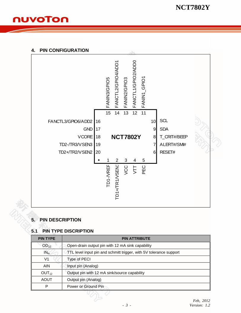
4. PIN CONFIGURATION
FA
NIN
3/G
PIO
5
FA
NC
TL2/G
PIO
4/A
DD
1
FA
NIN
2/G
PIO
3
FA
NC
TL1/G
PIO
2/A
DD
0
FA
NIN
1_G
PIO
1
15 14 13 12 11
FANCTL3/GPIO6/ADD2 16 10 SCL
GND 17 9 SDA
VCORE 18 8 T_CRIT#/BEEP
TD2-/TR3/VSEN3 19 7 ALERT#/SMI#
TD2+/TR2/VSEN2 20 6 RESET#
‧ 1 2 3 4 5
TD
1-/
VR
EF
TD
1+/T
R1/V
SE
N1
VC
C
VT
T
PE
CI
NCT7802Y
5. PIN DESCRIPTION
5.1 PIN TYPE DISCRIPTION
PIN TYPE PIN ATTRIBUTE
OD12 Open-drain output pin with 12 mA sink capability
INts TTL level input pin and schmitt trigger, with 5V tolerance support
V1 Type of PECI
AIN Input pin (Analog)
OUT12 Output pin with 12 mA sink/source capability
AOUT Output pin (Analog)
P Power or Ground Pin
NCT7802Y
Feb, 2012
- 4 - Version: 1.2
5.2 PIN DISCRIPTION
PIN NO. PIN NAME I/O FUNCTION
1 TD1- AIN Connect to Thermal Diode 1 Cathode
VREF AOUT VREF output for Thermistor function
2
TD1+
AIN
Connect to Thermal Diode 1 Anode
TR1 Thermistor 1 sensing input
VSEN1 Voltage sensing input. Detection range is 0~2.048V
3 VCC P Power supply, Voltage input 3.3V±5% It is also a voltage sensing input
4 VTT P Intel® CPU Vtt power
5 PECI V1 Intel® CPU PECI interface
6 RESET# OD12 Reset alarm output, for detect VCC power fault
7 ALERT#
OD12 Alarm output, for interrupt control (default)
SMI# Alarm output, for interrupt control
8
T_CRIT#
OD12
T_CRIT alarm output, for interrupt or shutdown control. (default)
BEEP BEEP output when abnormal event occurs (Frequency:300Hz/600Hz, Tone=500mS)
9 SDA INts/OD12 SMBus bi-directional data
10 SCL INts SMBus Clock
11
FANIN1 INts Fan tachometer input (default)
GPIO1 INts /OD12
/OUT12 General purpose I/O function
12
FANCTL1 OUT12/OD12
/AOUT
Fan speed control PWM/DC output
It can be configured to PWM/DC mode by registers. Default is PWM output
As DC output, 256 steps output voltage scaled to 0~VCC
GPIO2 INts /OD12
/OUT12 General purpose I/O function
13
FANIN2 INts Fan tachometer input (default)
GPIO3 INts /OD12
/OUT12 General purpose I/O function

NCT7802Y
Feb, 2012
- 5 - Version: 1.2
PIN NO. PIN NAME I/O FUNCTION
14
FANCTL2 OUT12/OD12
/AOUT
Fan speed control PWM/DC output
It can be configured to PWM/DC mode by registers. Default is PWM output
As DC output, 256 steps output voltage scaled to 0~VCC
GPIO4 INts /OD12
/OUT12 General purpose I/O function
15
FANIN3 INts Fan tachometer input (default)
GPIO5 INts /OD12
/OUT12 General purpose I/O function
16
FANCTL3 OUT12/OD12 Fan speed control PWM output
GPIO6 INts /OD12
/OUT12 General purpose I/O function
17 GND P Power supply ground
18 VCORE AIN Voltage sensing input. Detection range is 0~2.048V
19
TD2-
AIN
Connect to Thermal Diode 2 Cathode
TR3 Thermistor 3 sensing input
VSEN3 Voltage sensing input. Detection range is 0~2.048V
20
TD2+
AIN
Connect to Thermal Diode 2 Anode
TR2 Thermistor 2 sensing input
VSEN2 Voltage sensing input. Detection range is 0~2.048V
NCT7802Y
Feb, 2012
- 6 - Version: 1.2
6. DESCRIPTION
6.1 GENERAL DESCRIPTION
The NCT7802Y is a Nuvoton Hardware Monitor IC, contains one on-die and up to 5 remote temperature sensors, with SMBus and Intel PECI3.0 interface. There‟re also five voltage monitoring channels, 3 fan control groups, and GPIO functions with SMBus interface. NCT7802Y supports up to 8 sets SMBus address selection, it also provides ALERT#/SMI#/T_CRIT#/BEEP and RESET# alarm signals for event notification.
6.2 ACCESS INTERFACE
NCT7802Y provides SMBus to access the internal register, supports SMBus byte write and byte read protocols.
6.2.1 Data write to the internal register
6.2.2 Data read from the internal register
NCT7802Y
Feb, 2012
- 7 - Version: 1.2
6.3 ADDRESS SETTING
NCT7802Y has three address pins and multi-function with FANCTRL1~3, the SMBus address will be strapped when VCC ready 100mS, during the 100mS, the level of strapping pins must be fixed. The address will be retained as long as the VCC of NCT7802Y is maintained. The pull-up power plane must be the same as the VCC power of NCT7802Y.
ADD0(FANCTRL1) ADD1(FANCTRL2) ADD2(FANCTRL3) ADDRESS
0 0 0 0101 000X
0 0 1 0101 001X
0 1 0 0101 010X
0 1 1 0101 011X
1 0 0 0101 100X
1 0 1 0101 101X
1 1 0 0101 110X*1
1 1 1 0101 111X*2
X=Read/Write# Bit
*1 When set the NCT7802Y to address 5Ch, EEPROM loading function will be enabled, EEPROM address has to be ACh, refer to section 6.15.
*2 When set the NCT7802Y to address 5Eh, EEPROM loading function will be enabled, EEPROM address has to be AEh, refer to section 6.15.
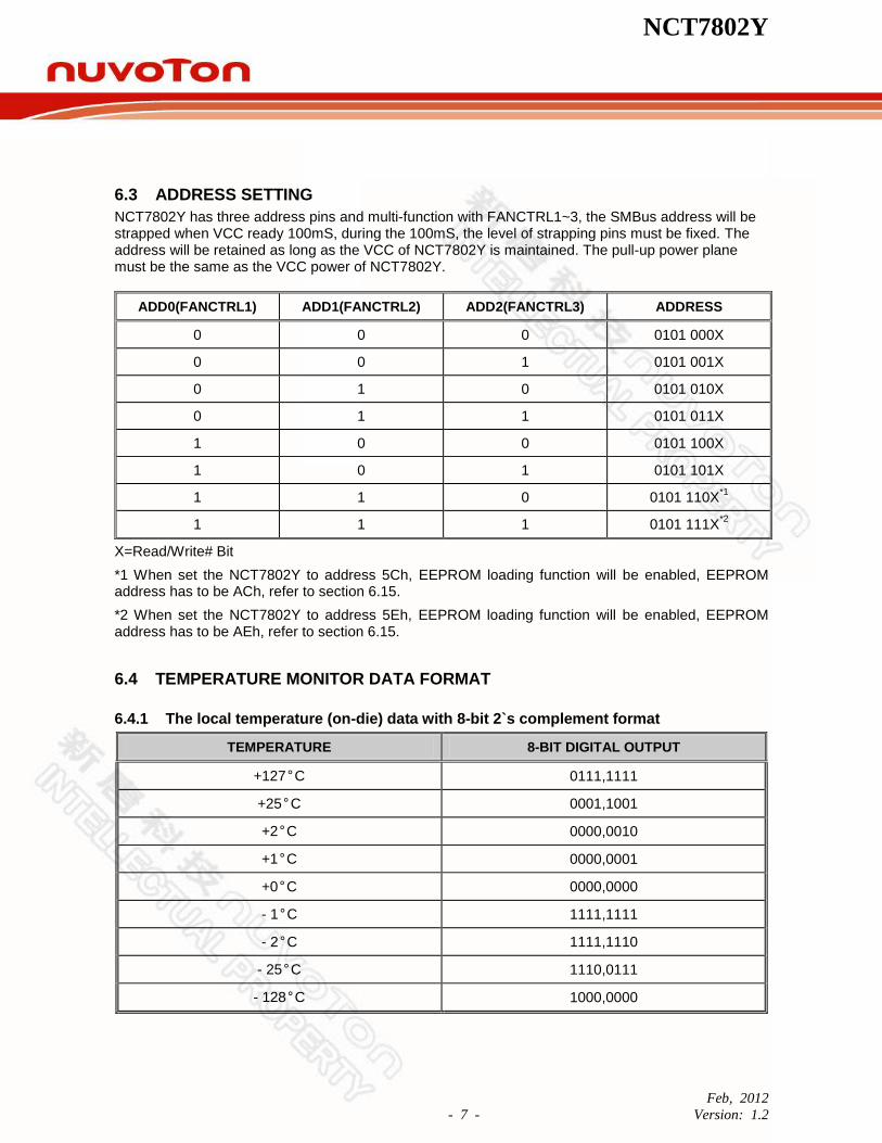
6.4 TEMPERATURE MONITOR DATA FORMAT
6.4.1 The local temperature (on-die) data with 8-bit 2`s complement format
TEMPERATURE 8-BIT DIGITAL OUTPUT
+127°C 0111,1111
+25°C 0001,1001
+2°C 0000,0010
+1°C 0000,0001
+0°C 0000,0000
- 1°C 1111,1111
- 2°C 1111,1110
- 25°C 1110,0111
- 128°C 1000,0000
NCT7802Y
Feb, 2012
- 8 - Version: 1.2
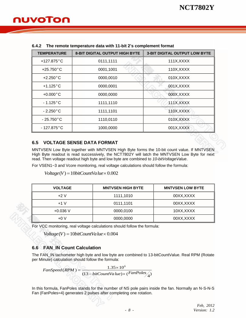
6.4.2 The remote temperature data with 11-bit 2’s complement format
TEMPERATURE 8-BIT DIGITAL OUTPUT HIGH BYTE 3-BIT DIGITAL OUTPUT LOW BYTE
+127.875°C 0111,1111 111X,XXXX
+25.750°C 0001,1001 110X,XXXX
+2.250°C 0000,0010 010X,XXXX
+1.125°C 0000,0001 001X,XXXX
+0.000°C 0000,0000 000X,XXXX
- 1.125°C 1111,1110 111X,XXXX
- 2.250°C 1111,1101 110X,XXXX
- 25.750°C 1110,0110 010X,XXXX
- 127.875°C 1000,0000 001X,XXXX
6.5 VOLTAGE SENSE DATA FORMAT
MNTVSEN Low Byte together with MNTVSEN High Byte forms the 10-bit count value. If MNTVSEN High Byte readout is read successively, the NCT7802Y will latch the MNTVSEN Low Byte for next read. Then voltage readout high byte and low byte are combined to 10-bitVoltageValue.
For VSEN1~3 and Vcore monitoring, real voltage calculations should follow the formula:
002.010)( luebitCountVaVVoltage
VOLTAGE MNTVSEN HIGH BYTE MNTVSEN LOW BYTE
+2 V 1111,1010 00XX,XXXX
+1 V 0111,1101 00XX,XXXX
+0.036 V 0000,0100 10XX,XXXX
+0 V 0000,0000 00XX,XXXX
For VCC monitoring, real voltage calculations should follow the formula:
004.010)( luebitCountVaVVoltage
6.6 FAN_IN Count Calculation
The FAN_IN tachometer high byte and low byte are combined to 13-bitCountValue. Real RPM (Rotate per Minute) calculation should follow the formula:
)4
()13(
1035.1)(
6
FanPolesluebitCountVaRPMSpeedFan
In this formula, FanPoles stands for the number of NS pole pairs inside the fan. Normally an N-S-N-S Fan (FanPoles=4) generates 2 pulses after completing one rotation.

NCT7802Y
Feb, 2012
- 9 - Version: 1.2
6.7 FAN_OUT Duty Cycle / DC Level Calculation
The NCT7802Y provides 3 set of PWM for fan speed control. The duty cycle of PWM can be programmed by an 8-bit register. The expression of duty cycle can be represented as follow formula:
%100255
ValueRegister bit -8 Programmed(%)cycleDuty
The NCT7802Y provides 2 set of DC output for fan speed control on FANCTL1 and FANCTL2. The DC output can be programmed by an 8-bit register. The expression of DC level can be represented as follow formula:
255
ValueRegister bit -8 Programmed)V( VoltageOutput VCC
6.8 SMART FANTM
IV Control Parameters
In SMART FANTM
IV Mode, there are some Fan control parameters as below descriptions:
6.8.1 Step Up Time / Step Down Time
SMART FANTM
IV is designed for the smooth operation of the fan. The Up Time / Down Time register defines the time interval between successive duty increases or decreases. If this value is set too small, the fan will not have enough time to speed up after tuning the duty and sometimes may result in unstable fan speed. On the other hand, if Up Time / Down Time is set too large, the fan may not work fast enough to dissipate the heat. This register should never be set to 0, otherwise, the fan duty will be abnormal.
6.8.2 Fan Output Start-up Value
From still to rotate, the fan usually needs a higher fan output value to generate enough torque to conquer the restriction force. Thus the Fan Output Start-up Value is used to turn on the fan with the specified output value.
6.8.3 Fan Output Nonstop
It takes some time to bring a fan from still to working state. Therefore, Nonstop value are designed with first FANCTL step output to keep the fan working when the system does not require the fan to help reduce heat but still want to keep the fast response time to speed up the fan.
6.8.4 Fan Output Stop Time
A time interval is specified to turn off the fan if SMART FANTM
IV continuously requests to slow down the fan which has already reached the Stop time.
DownTime
StopTime
UpTime
Non
Stop
Star
t
Smart Fan Lowering
FanSpeed
Smart Fan Arising Fan
Speed
FanSpeed
Figure 6-1 SMART FANTM
IV Control Parameters
NCT7802Y
Feb, 2012
- 10 - Version: 1.2
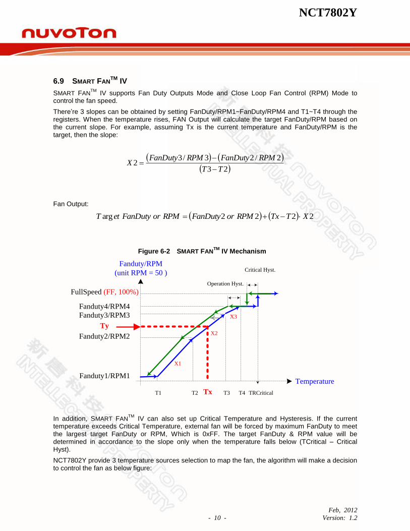
6.9 SMART FANTM
IV
SMART FANTM
IV supports Fan Duty Outputs Mode and Close Loop Fan Control (RPM) Mode to control the fan speed.
There‟re 3 slopes can be obtained by setting FanDuty/RPM1~FanDuty/RPM4 and T1~T4 through the registers. When the temperature rises, FAN Output will calculate the target FanDuty/RPM based on the current slope. For example, assuming Tx is the current temperature and FanDuty/RPM is the target, then the slope:
23
2/23/32
TT
RPMFanDutyRPMFanDutyX
Fan Output:
2222arg XTTxRPMorFanDutyRPMorFanDutyetT
Figure 6-2 SMART FANTM
IV Mechanism
Fanduty1/RPM1
Fanduty2/RPM2
FullSpeed (FF, 100%)
Operation Hyst.
TRCritical
Critical Hyst.
T1 T2 T3 T4
X2
X1
Fanduty3/RPM3
Fanduty4/RPM4
X3
Tx
Ty
Fanduty/RPM
(unit RPM = 50 )
Temperature
In addition, SMART FANTM
IV can also set up Critical Temperature and Hysteresis. If the current temperature exceeds Critical Temperature, external fan will be forced by maximum FanDuty to meet the largest target FanDuty or RPM, Which is 0xFF. The target FanDuty & RPM value will be determined in accordance to the slope only when the temperature falls below (TCritical – Critical Hyst).
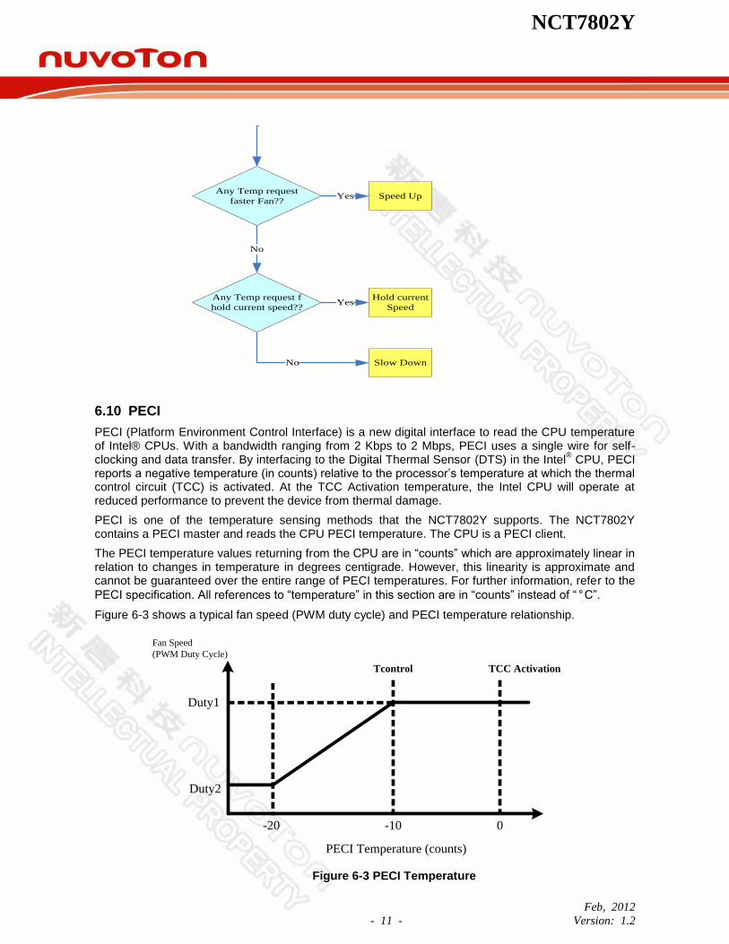
NCT7802Y provide 3 temperature sources selection to map the fan, the algorithm will make a decision to control the fan as below figure:
NCT7802Y
Feb, 2012
- 11 - Version: 1.2
Any Temp request
faster Fan??
Any Temp request f
hold current speed??
No
No
Speed Up
Hold current
Speed
Slow Down
Yes
Yes
6.10 PECI
PECI (Platform Environment Control Interface) is a new digital interface to read the CPU temperature of Intel® CPUs. With a bandwidth ranging from 2 Kbps to 2 Mbps, PECI uses a single wire for self-clocking and data transfer. By interfacing to the Digital Thermal Sensor (DTS) in the Intel
® CPU, PECI
reports a negative temperature (in counts) relative to the processor‟s temperature at which the thermal control circuit (TCC) is activated. At the TCC Activation temperature, the Intel CPU will operate at reduced performance to prevent the device from thermal damage.
PECI is one of the temperature sensing methods that the NCT7802Y supports. The NCT7802Y contains a PECI master and reads the CPU PECI temperature. The CPU is a PECI client.
The PECI temperature values returning from the CPU are in “counts” which are approximately linear in relation to changes in temperature in degrees centigrade. However, this linearity is approximate and cannot be guaranteed over the entire range of PECI temperatures. For further information, refer to the
PECI specification. All references to “temperature” in this section are in “counts” instead of “°C”.
Figure 6-3 shows a typical fan speed (PWM duty cycle) and PECI temperature relationship.
Tcontrol TCC Activation
Duty1
Duty2
-20 0-10
PECI Temperature (counts)
Fan Speed
(PWM Duty Cycle)
Figure 6-3 PECI Temperature
NCT7802Y
Feb, 2012
- 12 - Version: 1.2
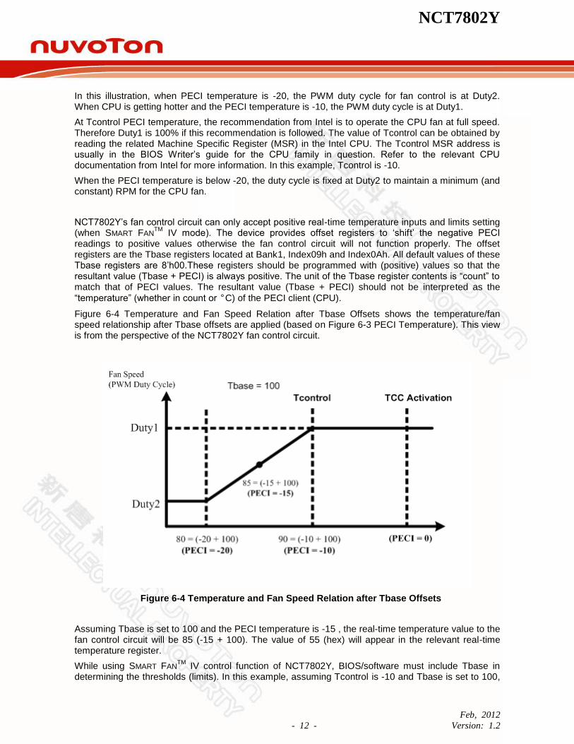
In this illustration, when PECI temperature is -20, the PWM duty cycle for fan control is at Duty2. When CPU is getting hotter and the PECI temperature is -10, the PWM duty cycle is at Duty1.
At Tcontrol PECI temperature, the recommendation from Intel is to operate the CPU fan at full speed. Therefore Duty1 is 100% if this recommendation is followed. The value of Tcontrol can be obtained by reading the related Machine Specific Register (MSR) in the Intel CPU. The Tcontrol MSR address is usually in the BIOS Writer‟s guide for the CPU family in question. Refer to the relevant CPU documentation from Intel for more information. In this example, Tcontrol is -10.
When the PECI temperature is below -20, the duty cycle is fixed at Duty2 to maintain a minimum (and constant) RPM for the CPU fan.
NCT7802Y‟s fan control circuit can only accept positive real-time temperature inputs and limits setting (when SMART FAN
TM IV mode). The device provides offset registers to „shift‟ the negative PECI
readings to positive values otherwise the fan control circuit will not function properly. The offset registers are the Tbase registers located at Bank1, Index09h and Index0Ah. All default values of these Tbase registers are 8‟h00.These registers should be programmed with (positive) values so that the resultant value (Tbase + PECI) is always positive. The unit of the Tbase register contents is “count” to match that of PECI values. The resultant value (Tbase + PECI) should not be interpreted as the
“temperature” (whether in count or °C) of the PECI client (CPU).
Figure 6-4 Temperature and Fan Speed Relation after Tbase Offsets shows the temperature/fan speed relationship after Tbase offsets are applied (based on Figure 6-3 PECI Temperature). This view is from the perspective of the NCT7802Y fan control circuit.
Figure 6-4 Temperature and Fan Speed Relation after Tbase Offsets
Assuming Tbase is set to 100 and the PECI temperature is -15 , the real-time temperature value to the fan control circuit will be 85 (-15 + 100). The value of 55 (hex) will appear in the relevant real-time temperature register.
While using SMART FANTM
IV control function of NCT7802Y, BIOS/software must include Tbase in determining the thresholds (limits). In this example, assuming Tcontrol is -10 and Tbase is set to 100,
NCT7802Y
Feb, 2012
- 13 - Version: 1.2
the threshold temperature value corresponding to the “100% fan duty cycle” event is 90 (-10+100). The value of 5A (hex) should be written to the relevant threshold register.
Tcontrol is typically -10 to -20 for PECI-enabled CPUs. Base on that, a value of 85 ~100 for Tbase could be set for proper operation of the fan control circuit. This recommendation is applicable for most designs. In general, the concept presented in this section could be used to determine the optimum value of Tcontrol to match the specific application.
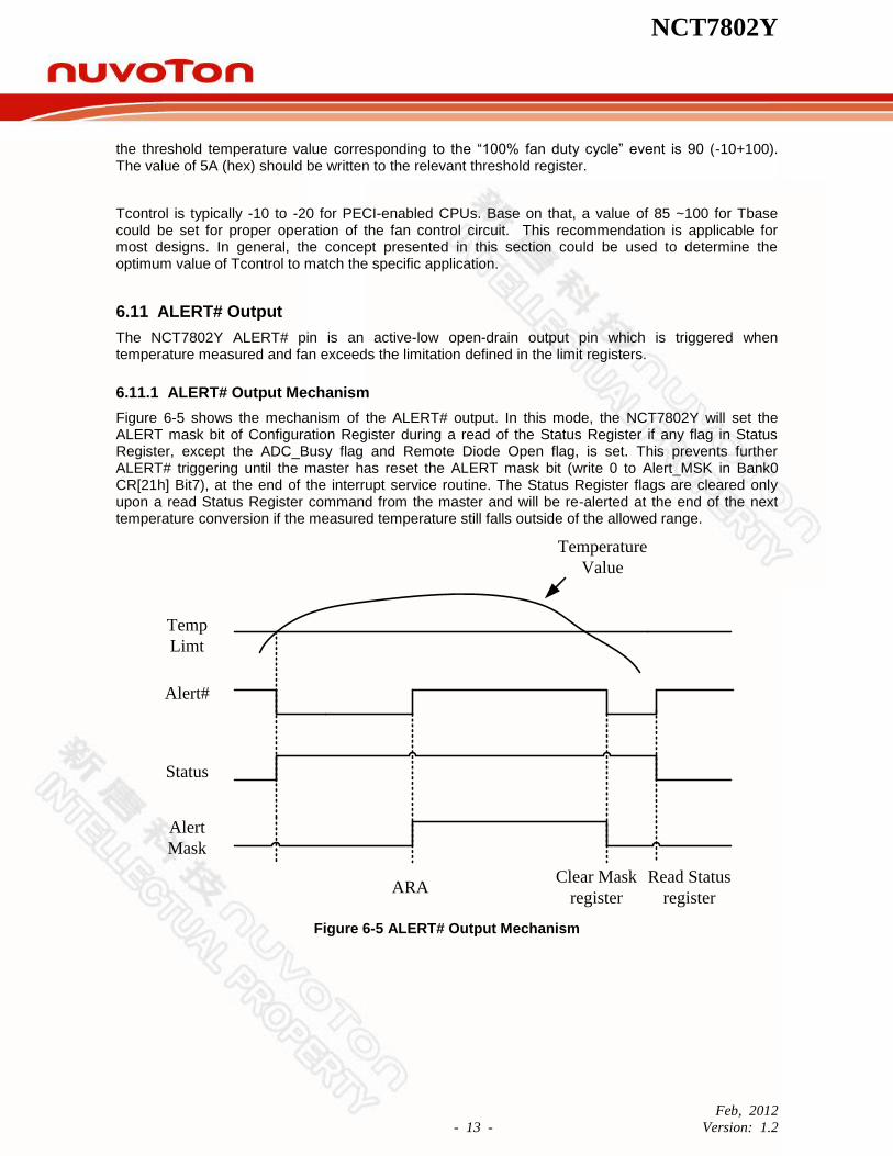
6.11 ALERT# Output
The NCT7802Y ALERT# pin is an active-low open-drain output pin which is triggered when temperature measured and fan exceeds the limitation defined in the limit registers.
6.11.1 ALERT# Output Mechanism
Figure 6-5 shows the mechanism of the ALERT# output. In this mode, the NCT7802Y will set the ALERT mask bit of Configuration Register during a read of the Status Register if any flag in Status Register, except the ADC_Busy flag and Remote Diode Open flag, is set. This prevents further ALERT# triggering until the master has reset the ALERT mask bit (write 0 to Alert_MSK in Bank0 CR[21h] Bit7), at the end of the interrupt service routine. The Status Register flags are cleared only upon a read Status Register command from the master and will be re-alerted at the end of the next temperature conversion if the measured temperature still falls outside of the allowed range.
Temp
Limt
Temperature
Value
Alert#
Status
Alert
Mask
Clear Mask
register
Read Status
registerARA
Figure 6-5 ALERT# Output Mechanism

NCT7802Y
Feb, 2012
- 14 - Version: 1.2
6.11.2 ALERT# Response Address
Figure 6-6 shows the mechanism of the SMBus ALERT# Response Address (ARA) support on ALERT# output. In this mode, the ALERT# output of the NCT7802Y is connected to the SMBus alert line which has more than one device connected to it. Through such and implementation, SMBus alert mode can assist the master in resolving which salve generates an interrupt. When the measured temperature falls outside of the allowed range, the ALERT# pin will be pulled low and the corresponding alert flags in Status Register will be set to 1. The ALERT# mask bit will just be set if there is a read command for Status Register or when ARA occurs from master (Alert Response Address is 0001100x). Meanwhile, the NCT7802Y will generate and return its own address to the master. If the temperature never falls outside of the allowed range, the latched ALERT# pin can release by the reset ALERT mask bit and the latched corresponding alert flags in Status Register can release by reading command for Status Register.
Figure 6-6 SMBus ARA Mechanism
6.12 T_CRIT# Output
T_CRIT# output pulls low when the measured temperature exceeds the critical temperature threshold point. Once the T_CRIT# output pulls low, it will not be set high until the measured temperature is lower than critical temperature threshold point.
6.13 SMI# Output
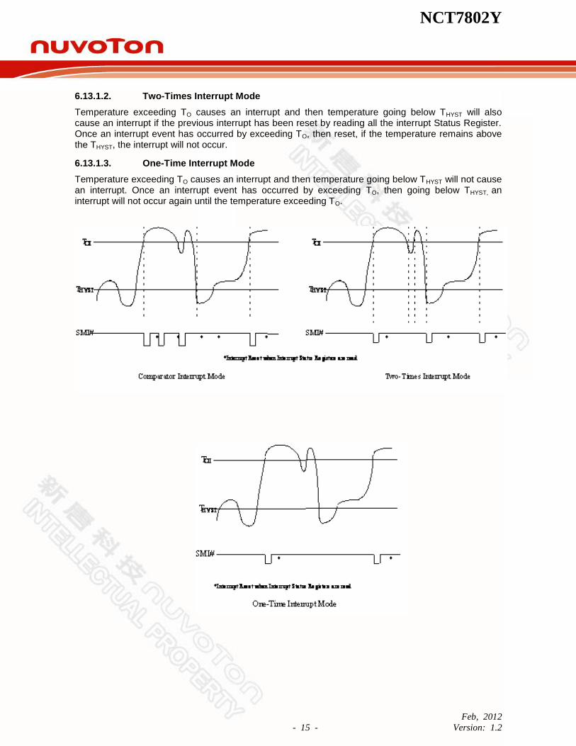
6.13.1 Temperature
SMI# for temperature monitoring provides 3 modes: Comparator Interrupt Mode, Two-Times Interrupt
Mode, and the One-Time Interrupt Mode.
6.13.1.1. Comparator Interrupt Mode
Temperature exceeding TO causes an interrupt and this interrupt will be reset when reading all of the Interrupt Status Registers. Once an interrupt event has occurred by exceeding TO, then reset, if the temperature remains above the THYST, the interrupt will occur again when the next conversion has completed. If an interrupt event has occurred by exceeding TO and not reset, the interrupts will not occur again. The interrupts will continue to occur in this manner until the temperature goes below THYST.
NCT7802Y
Feb, 2012
- 15 - Version: 1.2
6.13.1.2. Two-Times Interrupt Mode
Temperature exceeding TO causes an interrupt and then temperature going below THYST will also cause an interrupt if the previous interrupt has been reset by reading all the interrupt Status Register. Once an interrupt event has occurred by exceeding TO, then reset, if the temperature remains above the THYST, the interrupt will not occur.
6.13.1.3. One-Time Interrupt Mode
Temperature exceeding TO causes an interrupt and then temperature going below THYST will not cause an interrupt. Once an interrupt event has occurred by exceeding TO, then going below THYST, an interrupt will not occur again until the temperature exceeding TO.
NCT7802Y
Feb, 2012
- 16 - Version: 1.2
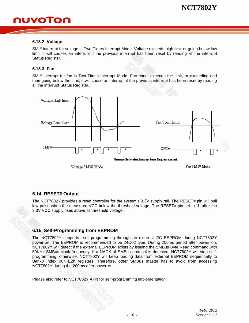
6.13.2 Voltage
SMI# interrupt for voltage is Two-Times Interrupt Mode. Voltage exceeds high limit or going below low limit, it will causes an interrupt if the previous interrupt has been reset by reading all the interrupt Status Register.
6.13.3 Fan
SMI# interrupt for fan is Two-Times Interrupt Mode. Fan count exceeds the limit, or exceeding and then going below the limit, it will cause an interrupt if the previous interrupt has been reset by reading all the interrupt Status Register.
6.14 RESET# Output
The NCT7802Y provides a reset controller for the system‟s 3.3V supply rail. The RESET# pin will pull low pulse when the measured VCC below the threshold voltage. The RESET# pin set to „1‟ after the 3.3V VCC supply rises above its threshold voltage.
6.15 Self-Programming from EEPROM
The NCT7802Y supports self-programming through an external I2C EEPROM during NCT7802Y power-on. The EEPROM is recommended to be 24C02 type. During 200ms period after power on, NCT7802Y will detect if the external EEPROM exists by issuing the SMBus Byte Read command with 50KHz SMBus clock frequency. If a NACK of SMBus protocol is detected, NCT7802Y will stop self-programming, otherwise, NCT7802Y will keep loading data from external EEPROM sequentially to Bank0 Index 00h~E2h registers. Therefore, other SMBus master has to avoid from accessing NCT7802Y during the 200ms after power-on.
Please also refer to NCT7802Y APN for self-programming implementation.
NCT7802Y
Feb, 2012
- 17 - Version: 1.2
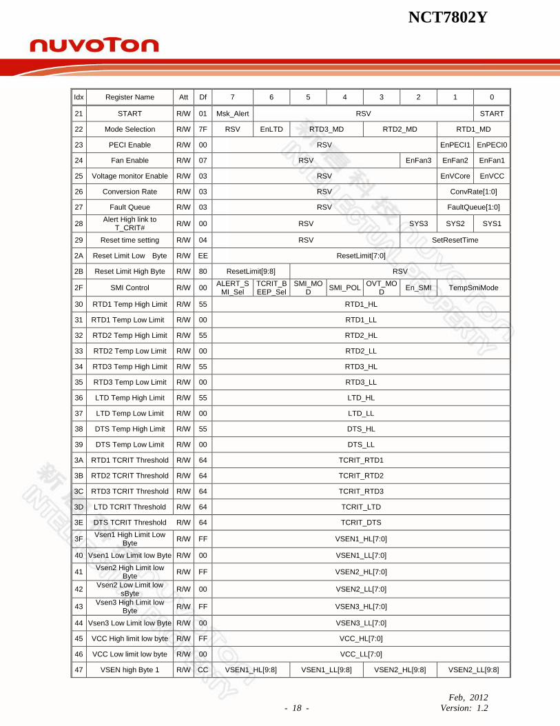
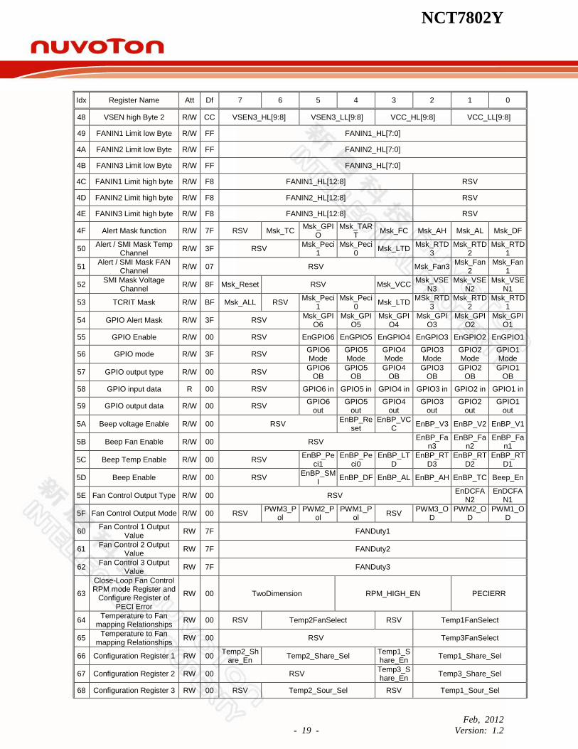
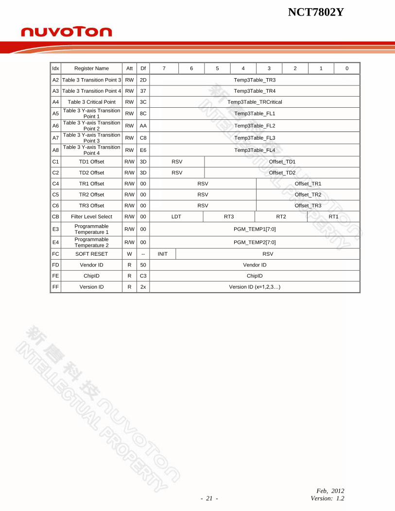
7. REGISTER DESCRIPTION
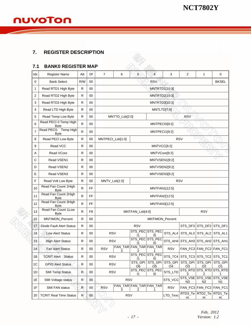
7.1 BANK0 REGISTER MAP
Idx Register Name Att Df 7 6 5 4 3 2 1 0
0 Bank Select R/W 00 RSV BKSEL
1 Read RTD1 High Byte R 00 MNTRTD1[10:3]
2 Read RTD2 High Byte R 00 MNTRTD2[10:3]
3 Read RTD3 High Byte R 00 MNTRTD3[10:3]
4 Read LTD High Byte R 00 MNTLTD[7:0]
5 Read Temp Low Byte R 00 MNTTD_Lsb[2:0] RSV
6 Read PECI 0 Temp High
Byte R 00 MNTPECI0[9:2]
7 Read PECI1 Temp High
Byte R 00 MNTPECI1[9:2]
8 Read PECI Low Byte R 00 MNTPECI_Lsb[1:0] RSV
9 Read VCC R 00 MNTVCC[9:2]
A Read VCore R 00 MNTVCore[9:2]
C Read VSEN1 R 00 MNTVSEN1[9:2]
D Read VSEN2 R 00 MNTVSEN2[9:2]
E Read VSEN3 R 00 MNTVSEN3[9:2]
F Read Volt Low Byte R 00 MNTV_Lsb[1:0] RSV
10 Read Fan Count 1High
Byte R FF MNTFAN1[12:5]
11 Read Fan Count 2High
Byte R FF MNTFAN2[12:5]
12 Read Fan Count 3High
Byte R FF MNTFAN3[12:5]
13 Read Fan Count 1Low
Byte R F8 MNTFAN_Lsb[4:0] RSV
15 MNTIMON_Percent R 00 MNTIMON_Percent
17 Diode Fault Alert Status R 00 RSV STS_DF3 STS_DF2 STS_DF1
18 Low Alert Status R 00 RSV STS_PEC
I1 STS_PEC
I0 STS_AL4 STS_AL3 STS_AL2 STS_AL1
19 High Alert Status R 00 RSV STS_PEC
I1 STS_PEC
I0 STS_AH4 STS_AH3 STS_AH2 STS_AH1
1A Fan Alert Status R 00 RSV FAN_TAR
3 FAN_TAR
2 FAN_TAR
1 RSV FAN_FC3 FAN_FC2 FAN_FC1
1B TCRIT Alert Status R 00 RSV STS_PEC
I1 STS_PEC
I0 STS_TC4 STS_TC3 STS_TC2 STS_TC1
1C GPIO Alert Status R 00 RSV STS_GPI
O6 STS_GPI
O5 STS_GPI
O4 STS_GPI
O3 STS_GPI
O2 STS_GPI
O1
1D SMI Temp Status R 00 RSV STS_PEC
I1 STS_PEC
I0 STS_LTD
STS_RTD3
STS_RTD2
STS_RTD1
1E SMI Voltage status R 00 RSV STS_VCC STS_VSE
N3 STS_VSE
N2 STS_VSE
N1
1F SMI FAN status R 00 RSV FAN_TAR
3 FAN_TAR
2 FAN_TAR
1 RSV FAN_FC3 FAN_FC2 FAN_FC1
20 TCRIT Real Time Status R 00 RSV LTD_Texc RTD3_Te
xc RTD2_Te
xc RTD1_Te
xc
NCT7802Y
Feb, 2012
- 18 - Version: 1.2
Idx Register Name Att Df 7 6 5 4 3 2 1 0
21 START R/W 01 Msk_Alert RSV START
22 Mode Selection R/W 7F RSV EnLTD RTD3_MD RTD2_MD RTD1_MD
23 PECI Enable R/W 00 RSV EnPECI1 EnPECI0
24 Fan Enable R/W 07 RSV EnFan3 EnFan2 EnFan1
25 Voltage monitor Enable R/W 03 RSV EnVCore EnVCC
26 Conversion Rate R/W 03 RSV ConvRate[1:0]
27 Fault Queue R/W 03 RSV FaultQueue[1:0]
28 Alert High link to
T_CRIT# R/W 00 RSV SYS3 SYS2 SYS1
29 Reset time setting R/W 04 RSV SetResetTime
2A Reset Limit Low Byte R/W EE ResetLimit[7:0]
2B Reset Limit High Byte R/W 80 ResetLimit[9:8] RSV
2F SMI Control R/W 00 ALERT_S
MI_Sel TCRIT_BEEP_Sel
SMI_MOD
SMI_POL OVT_MO
D En_SMI TempSmiMode
30 RTD1 Temp High Limit R/W 55 RTD1_HL
31 RTD1 Temp Low Limit R/W 00 RTD1_LL
32 RTD2 Temp High Limit R/W 55 RTD2_HL
33 RTD2 Temp Low Limit R/W 00 RTD2_LL
34 RTD3 Temp High Limit R/W 55 RTD3_HL
35 RTD3 Temp Low Limit R/W 00 RTD3_LL
36 LTD Temp High Limit R/W 55 LTD_HL
37 LTD Temp Low Limit R/W 00 LTD_LL
38 DTS Temp High Limit R/W 55 DTS_HL
39 DTS Temp Low Limit R/W 00 DTS_LL
3A RTD1 TCRIT Threshold R/W 64 TCRIT_RTD1
3B RTD2 TCRIT Threshold R/W 64 TCRIT_RTD2
3C RTD3 TCRIT Threshold R/W 64 TCRIT_RTD3
3D LTD TCRIT Threshold R/W 64 TCRIT_LTD
3E DTS TCRIT Threshold R/W 64 TCRIT_DTS
3F Vsen1 High Limit Low
Byte R/W FF VSEN1_HL[7:0]
40 Vsen1 Low Limit low Byte R/W 00 VSEN1_LL[7:0]
41 Vsen2 High Limit low
Byte R/W FF VSEN2_HL[7:0]
42 Vsen2 Low Limit low
sByte R/W 00 VSEN2_LL[7:0]
43 Vsen3 High Limit low
Byte R/W FF VSEN3_HL[7:0]
44 Vsen3 Low Limit low Byte R/W 00 VSEN3_LL[7:0]
45 VCC High limit low byte R/W FF VCC_HL[7:0]
46 VCC Low limit low byte R/W 00 VCC_LL[7:0]
47 VSEN high Byte 1 R/W CC VSEN1_HL[9:8] VSEN1_LL[9:8] VSEN2_HL[9:8] VSEN2_LL[9:8]
NCT7802Y
Feb, 2012
- 19 - Version: 1.2
Idx Register Name Att Df 7 6 5 4 3 2 1 0
48 VSEN high Byte 2 R/W CC VSEN3_HL[9:8] VSEN3_LL[9:8] VCC_HL[9:8] VCC_LL[9:8]
49 FANIN1 Limit low Byte R/W FF FANIN1_HL[7:0]
4A FANIN2 Limit low Byte R/W FF FANIN2_HL[7:0]
4B FANIN3 Limit low Byte R/W FF FANIN3_HL[7:0]
4C FANIN1 Limit high byte R/W F8 FANIN1_HL[12:8] RSV
4D FANIN2 Limit high byte R/W F8 FANIN2_HL[12:8] RSV
4E FANIN3 Limit high byte R/W F8 FANIN3_HL[12:8] RSV
4F Alert Mask function R/W 7F RSV Msk_TC Msk_GPI
O Msk_TAR
T Msk_FC Msk_AH Msk_AL Msk_DF
50 Alert / SMI Mask Temp
Channel R/W 3F RSV
Msk_Peci1
Msk_Peci0
Msk_LTD Msk_RTD
3 Msk_RTD
2 Msk_RTD
1
51 Alert / SMI Mask FAN
Channel R/W 07 RSV Msk_Fan3
Msk_Fan2
Msk_Fan1
52 SMI Mask Voltage
Channel R/W 8F Msk_Reset RSV Msk_VCC
Msk_VSEN3
Msk_VSEN2
Msk_VSEN1
53 TCRIT Mask R/W BF Msk_ALL RSV Msk_Peci
1 Msk_Peci
0 Msk_LTD
MSk_RTD3
Msk_RTD2
Msk_RTD1
54 GPIO Alert Mask R/W 3F RSV Msk_GPI
O6 Msk_GPI
O5 Msk_GPI
O4 Msk_GPI
O3 Msk_GPI
O2 Msk_GPI
O1
55 GPIO Enable R/W 00 RSV EnGPIO6 EnGPIO5 EnGPIO4 EnGPIO3 EnGPIO2 EnGPIO1
56 GPIO mode R/W 3F RSV GPIO6 Mode
GPIO5 Mode
GPIO4 Mode
GPIO3 Mode
GPIO2 Mode
GPIO1 Mode
57 GPIO output type R/W 00 RSV GPIO6
OB GPIO5
OB GPIO4
OB GPIO3
OB GPIO2
OB GPIO1
OB
58 GPIO input data R 00 RSV GPIO6 in GPIO5 in GPIO4 in GPIO3 in GPIO2 in GPIO1 in
59 GPIO output data R/W 00 RSV GPIO6
out GPIO5
out GPIO4
out GPIO3
out GPIO2
out GPIO1
out
5A Beep voltage Enable R/W 00 RSV EnBP_Re
set EnBP_VC
C EnBP_V3 EnBP_V2 EnBP_V1
5B Beep Fan Enable R/W 00 RSV EnBP_Fa
n3 EnBP_Fa
n2 EnBP_Fa
n1
5C Beep Temp Enable R/W 00 RSV EnBP_Pe
ci1 EnBP_Pe
ci0 EnBP_LT
D EnBP_RT
D3 EnBP_RT
D2 EnBP_RT
D1
5D Beep Enable R/W 00 RSV EnBP_SM
I EnBP_DF EnBP_AL EnBP_AH EnBP_TC Beep_En
5E Fan Control Output Type R/W 00 RSV EnDCFA
N2 EnDCFA
N1
5F Fan Control Output Mode R/W 00 RSV PWM3_P
ol PWM2_P
ol PWM1_P
ol RSV
PWM3_OD
PWM2_OD
PWM1_OD
60 Fan Control 1 Output
Value RW 7F FANDuty1
61 Fan Control 2 Output
Value RW 7F FANDuty2
62 Fan Control 3 Output
Value RW 7F FANDuty3
63
Close-Loop Fan Control RPM mode Register and
Configure Register of PECI Error
RW 00 TwoDimension RPM_HIGH_EN PECIERR
64 Temperature to Fan
mapping Relationships RW 00 RSV Temp2FanSelect RSV Temp1FanSelect
65 Temperature to Fan
mapping Relationships RW 00 RSV Temp3FanSelect
66 Configuration Register 1 RW 00 Temp2_Sh
are_En Temp2_Share_Sel
Temp1_Share_En
Temp1_Share_Sel
67 Configuration Register 2 RW 00 RSV Temp3_Share_En
Temp3_Share_Sel
68 Configuration Register 3 RW 00 RSV Temp2_Sour_Sel RSV Temp1_Sour_Sel

NCT7802Y
Feb, 2012
- 20 - Version: 1.2
Idx Register Name Att Df 7 6 5 4 3 2 1 0
69 Configuration Register 4 RW 00 RSV Temp3_Sour_Sel
6D Close-Loop Fan Control RPM mode Tolerance
RW 02 RSV Generic_Tol_RPM
6E Fanctl Step Up Time RW 0A UpTime
6F Fanctl Step Down Time RW 0A DownTime
70 DefaultFanSpeed RW 7F DefaultFanSpeed
71 PWM1 Prescalar RW 84 FanOutDivi
sor1[7] FanOutDivisor1[6:0]
72 PWM2 Prescalar RW 84 FanOutDivi
sor2[7] FanOutDivisor2[6:0]
73 PWM3 Prescalar RW 84 FanOutDivi
sor3[7] FanOutDivisor3[6:0]
74 Temp1 Hystersis RW 53 RSV Criti_HysT1 RSV Oper_HysT1
75 Temp2 Hystersis RW 53 RSV Criti_HysT2 RSV Oper_HysT2
76 Temp3 Hystersis RW 53 RSV Criti_HysT3 RSV Oper_HysT3
77 Fanctl Start Duty Cycle RW 30 StartDutyCycle
78 Stop Time of Fanctl RW FF StopTime
79 NonStop Enable RW 00 RSV NonStop
7A Fan Output Min Value
when PECI Error RW 80 MinDuty_PECIERR
80 Table 1 Transition Point 1 RW 19 Temp1Table_TR1
81 Table 1 Transition Point 2 RW 23 Temp1Table_TR2
82 Table 1 Transition Point 3 RW 2D Temp1Table_TR3
83 Table 1 Transition Point 4 RW 37 Temp1Table_TR4
84 Table 1 Critical Point RW 3C Temp1Table_TRCritical
85 Table 1 Y-axis Transition
Point 1 RW 8C Temp1Table_FL1
86 Table 1 Y-axis Transition
Point 2 RW AA Temp1Table_FL2
87 Table 1 Y-axis Transition
Point 3 RW C8 Temp1Table_FL3
88 Table 1 Y-axis Transition
Point 4 RW E6 Temp1Table_FL4
90 Table 2 Transition Point 1 RW 19 Temp2Table_TR1
91 Table 2 Transition Point 2 RW 23 Temp2Table_TR2
92 Table 2 Transition Point 3 RW 2D Temp2Table_TR3
93 Table 2 Transition Point 4 RW 37 Temp2Table_TR4
94 Table 2 Critical Point RW 3C Temp2Table_TRCritical
95 Table 2 Y-axis Transition
Point 1 RW 8C Temp2Table_FL1
96 Table 2 Y-axis Transition
Point 2 RW AA Temp2Table_FL2
97 Table 2 Y-axis Transition
Point 3 RW C8 Temp2Table_FL3
98 Table 2 Y-axis Transition
Point 4 RW E6 Temp2Table_FL4
A0 Table 3 Transition Point 1 RW 19 Temp3Table_TR1
A1 Table 3 Transition Point 2 RW 23 Temp3Table_TR2
NCT7802Y
Feb, 2012
- 21 - Version: 1.2
Idx Register Name Att Df 7 6 5 4 3 2 1 0
A2 Table 3 Transition Point 3 RW 2D Temp3Table_TR3
A3 Table 3 Transition Point 4 RW 37 Temp3Table_TR4
A4 Table 3 Critical Point RW 3C Temp3Table_TRCritical
A5 Table 3 Y-axis Transition
Point 1 RW 8C Temp3Table_FL1
A6 Table 3 Y-axis Transition
Point 2 RW AA Temp3Table_FL2
A7 Table 3 Y-axis Transition
Point 3 RW C8 Temp3Table_FL3
A8 Table 3 Y-axis Transition
Point 4 RW E6 Temp3Table_FL4
C1 TD1 Offset R/W 3D RSV Offset_TD1
C2 TD2 Offset R/W 3D RSV Offset_TD2
C4 TR1 Offset R/W 00 RSV Offset_TR1
C5 TR2 Offset R/W 00 RSV Offset_TR2
C6 TR3 Offset R/W 00 RSV Offset_TR3
CB Filter Level Select R/W 00 LDT RT3 RT2 RT1
E3 Programmable Temperature 1
R/W 00 PGM_TEMP1[7:0]
E4 Programmable Temperature 2
R/W 00 PGM_TEMP2[7:0]
FC SOFT RESET W -- INIT RSV
FD Vendor ID R 50 Vendor ID
FE ChipID R C3 ChipID
FF Version ID R 2x Version ID (x=1,2,3…)
NCT7802Y
Feb, 2012
- 22 - Version: 1.2
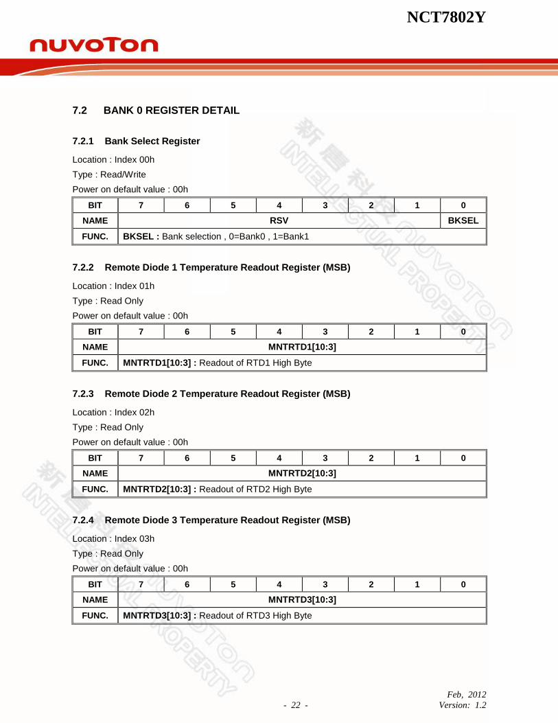
7.2 BANK 0 REGISTER DETAIL
7.2.1 Bank Select Register
Location : Index 00h
Type : Read/Write
Power on default value : 00h
BIT 7 6 5 4 3 2 1 0
NAME RSV BKSEL
FUNC. BKSEL : Bank selection , 0=Bank0 , 1=Bank1
7.2.2 Remote Diode 1 Temperature Readout Register (MSB)
Location : Index 01h
Type : Read Only
Power on default value : 00h
BIT 7 6 5 4 3 2 1 0
NAME MNTRTD1[10:3]
FUNC. MNTRTD1[10:3] : Readout of RTD1 High Byte
7.2.3 Remote Diode 2 Temperature Readout Register (MSB)
Location : Index 02h
Type : Read Only
Power on default value : 00h
BIT 7 6 5 4 3 2 1 0
NAME MNTRTD2[10:3]
FUNC. MNTRTD2[10:3] : Readout of RTD2 High Byte
7.2.4 Remote Diode 3 Temperature Readout Register (MSB)
Location : Index 03h
Type : Read Only
Power on default value : 00h
BIT 7 6 5 4 3 2 1 0
NAME MNTRTD3[10:3]
FUNC. MNTRTD3[10:3] : Readout of RTD3 High Byte
NCT7802Y
Feb, 2012
- 23 - Version: 1.2
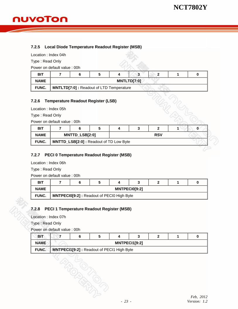
7.2.5 Local Diode Temperature Readout Register (MSB)
Location : Index 04h
Type : Read Only
Power on default value : 00h
BIT 7 6 5 4 3 2 1 0
NAME MNTLTD[7:0]
FUNC. MNTLTD[7:0] : Readout of LTD Temperature
7.2.6 Temperature Readout Register (LSB)
Location : Index 05h
Type : Read Only
Power on default value : 00h
BIT 7 6 5 4 3 2 1 0
NAME MNTTD_LSB[2:0] RSV
FUNC. MNTTD_LSB[2:0] : Readout of TD Low Byte
7.2.7 PECI 0 Temperature Readout Register (MSB)
Location : Index 06h
Type : Read Only
Power on default value : 00h
BIT 7 6 5 4 3 2 1 0
NAME MNTPECI0[9:2]
FUNC. MNTPECI0[9:2] : Readout of PECI0 High Byte
7.2.8 PECI 1 Temperature Readout Register (MSB)
Location : Index 07h
Type : Read Only
Power on default value : 00h
BIT 7 6 5 4 3 2 1 0
NAME MNTPECI1[9:2]
FUNC. MNTPECI1[9:2] : Readout of PECI1 High Byte

NCT7802Y
Feb, 2012
- 24 - Version: 1.2
7.2.9 Read PECI Temperature Readout Register (LSB)
Location : Index 08h
Type : Read Only
Power on default value : 00h
BIT 7 6 5 4 3 2 1 0
NAME MNTPECI_LSB[1:0] RSV
FUNC. MNTPECI_LSB[1:0] : Readout of PECI Low Byte
7.2.10 VCC Readout Register (MSB)
Location : Index 09h
Type : Read Only
Power on default value : 00h
BIT 7 6 5 4 3 2 1 0
NAME MNTVCC[9:2]
FUNC. MNTVCC[9:2] : Readout of VCC High Byte
7.2.11 VCore Readout Register (MSB)
Location : Index 0Ah
Type : Read Only
Power on default value : 00h
BIT 7 6 5 4 3 2 1 0
NAME MNTVCore[9:2]
FUNC. MNTVCore[9:2] : Readout of VCore High Byte
7.2.12 VSEN1 Readout Register (MSB)
Location : Index 0Ch
Type : Read Only
Power on default value : 00h
BIT 7 6 5 4 3 2 1 0
NAME MNTVSEN1[9:2]
FUNC. MNTVSEN1[9:2] : Readout of VSEN1 High Byte

NCT7802Y
Feb, 2012
- 25 - Version: 1.2
7.2.13 VSEN2 Readout Register (MSB)
Location : Index 0Dh
Type : Read Only
Power on default value : 00h
BIT 7 6 5 4 3 2 1 0
NAME MNTVSEN2[9:2]
FUNC. MNTVSEN2[9:2] : Readout of VSEN2 High Byte
7.2.14 VSEN3 Readout Register (MSB)
Location : Index 0Eh
Type : Read Only
Power on default value : 00h
BIT 7 6 5 4 3 2 1 0
NAME MNTVSEN3[9:2]
FUNC. MNTVSEN3[9:2] : Readout of VSEN3 High Byte
7.2.15 Voltage Readout Register (LSB)
Location : Index 0Fh
Type : Read Only
Power on default value : 00h
BIT 7 6 5 4 3 2 1 0
NAME MNTV_LSB[1:0] RSV
FUNC. MNTV_LSB[1:0] : Readout of Voltage Low Byte
7.2.16 Fan Count 1 Readout Register (MSB)
Location : Index 10h
Type : Read Only
Power on default value : FFh
BIT 7 6 5 4 3 2 1 0
NAME MNTFAN1[12:5]
FUNC. MNTFAN1[12:5] : Readout of Fan Count 1 High Byte
NCT7802Y
Feb, 2012
- 26 - Version: 1.2
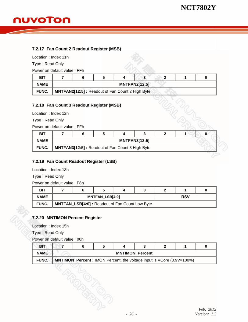
7.2.17 Fan Count 2 Readout Register (MSB)
Location : Index 11h
Type : Read Only
Power on default value : FFh
BIT 7 6 5 4 3 2 1 0
NAME MNTFAN2[12:5]
FUNC. MNTFAN2[12:5] : Readout of Fan Count 2 High Byte
7.2.18 Fan Count 3 Readout Register (MSB)
Location : Index 12h
Type : Read Only
Power on default value : FFh
BIT 7 6 5 4 3 2 1 0
NAME MNTFAN3[12:5]
FUNC. MNTFAN3[12:5] : Readout of Fan Count 3 High Byte
7.2.19 Fan Count Readout Register (LSB)
Location : Index 13h
Type : Read Only
Power on default value : F8h
BIT 7 6 5 4 3 2 1 0
NAME MNTFAN_LSB[4:0] RSV
FUNC. MNTFAN_LSB[4:0] : Readout of Fan Count Low Byte
7.2.20 MNTIMON Percent Register
Location : Index 15h
Type : Read Only
Power on default value : 00h
BIT 7 6 5 4 3 2 1 0
NAME MNTIMON_Percent
FUNC. MNTIMON_Percent : IMON Percent, the voltage input is VCore (0.9V=100%)
NCT7802Y
Feb, 2012
- 27 - Version: 1.2
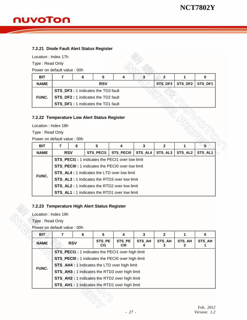
7.2.21 Diode Fault Alert Status Register
Location : Index 17h
Type : Read Only
Power on default value : 00h
BIT 7 6 5 4 3 2 1 0
NAME RSV STS_DF3 STS_DF2 STS_DF1
FUNC.
STS_DF3 : 1 indicates the TD3 fault
STS_DF2 : 1 indicates the TD2 fault
STS_DF1 : 1 indicates the TD1 fault
7.2.22 Temperature Low Alert Status Register
Location : Index 18h
Type : Read Only
Power on default value : 00h
BIT 7 6 5 4 3 2 1 0
NAME RSV STS_PECI1 STS_PECI0 STS_AL4 STS_AL3 STS_AL2 STS_AL1
FUNC.
STS_PECI1 : 1 indicates the PECI1 over low limit
STS_PECI0 : 1 indicates the PECI0 over low limit
STS_AL4 : 1 indicates the LTD over low limit
STS_AL3 : 1 indicates the RTD3 over low limit
STS_AL2 : 1 indicates the RTD2 over low limit
STS_AL1 : 1 indicates the RTD1 over low limit
7.2.23 Temperature High Alert Status Register
Location : Index 19h
Type : Read Only
Power on default value : 00h
BIT 7 6 5 4 3 2 1 0
NAME RSV STS_PE
CI1 STS_PE
CI0 STS_AH
4 STS_AH
3 STS_AH
2 STS_AH
1
FUNC.
STS_PECI1 : 1 indicates the PECI1 over high limit
STS_PECI0 : 1 indicates the PECI0 over high limit
STS_AH4 : 1 indicates the LTD over high limit
STS_AH3 : 1 indicates the RTD3 over high limit
STS_AH2 : 1 indicates the RTD2 over high limit
STS_AH1 : 1 indicates the RTD1 over high limit
NCT7802Y
Feb, 2012
- 28 - Version: 1.2
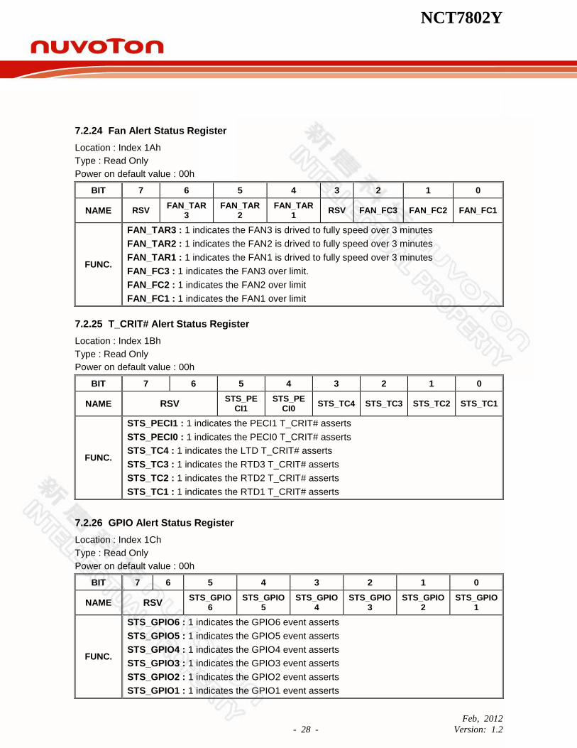
7.2.24 Fan Alert Status Register
Location : Index 1Ah
Type : Read Only
Power on default value : 00h
BIT 7 6 5 4 3 2 1 0
NAME RSV FAN_TAR
3 FAN_TAR
2 FAN_TAR
1 RSV FAN_FC3 FAN_FC2 FAN_FC1
FUNC.
FAN_TAR3 : 1 indicates the FAN3 is drived to fully speed over 3 minutes
FAN_TAR2 : 1 indicates the FAN2 is drived to fully speed over 3 minutes
FAN_TAR1 : 1 indicates the FAN1 is drived to fully speed over 3 minutes
FAN_FC3 : 1 indicates the FAN3 over limit.
FAN_FC2 : 1 indicates the FAN2 over limit
FAN_FC1 : 1 indicates the FAN1 over limit
7.2.25 T_CRIT# Alert Status Register
Location : Index 1Bh
Type : Read Only
Power on default value : 00h
BIT 7 6 5 4 3 2 1 0
NAME RSV STS_PE
CI1 STS_PE
CI0 STS_TC4 STS_TC3 STS_TC2 STS_TC1
FUNC.
STS_PECI1 : 1 indicates the PECI1 T_CRIT# asserts
STS_PECI0 : 1 indicates the PECI0 T_CRIT# asserts
STS_TC4 : 1 indicates the LTD T_CRIT# asserts
STS_TC3 : 1 indicates the RTD3 T_CRIT# asserts
STS_TC2 : 1 indicates the RTD2 T_CRIT# asserts
STS_TC1 : 1 indicates the RTD1 T_CRIT# asserts
7.2.26 GPIO Alert Status Register
Location : Index 1Ch
Type : Read Only
Power on default value : 00h
BIT 7 6 5 4 3 2 1 0
NAME RSV STS_GPIO
6 STS_GPIO
5 STS_GPIO
4 STS_GPIO
3 STS_GPIO
2 STS_GPIO
1
FUNC.
STS_GPIO6 : 1 indicates the GPIO6 event asserts
STS_GPIO5 : 1 indicates the GPIO5 event asserts
STS_GPIO4 : 1 indicates the GPIO4 event asserts
STS_GPIO3 : 1 indicates the GPIO3 event asserts
STS_GPIO2 : 1 indicates the GPIO2 event asserts
STS_GPIO1 : 1 indicates the GPIO1 event asserts

NCT7802Y
Feb, 2012
- 29 - Version: 1.2
7.2.27 Temperature SMI Status Register
Location : Index 1Dh
Type : Read Only
Power on default value : 00h
BIT 7 6 5 4 3 2 1 0
NAME RSV STS_PE
CI1 STS_PE
CI0 STS_LT
D4 STS_RT
D3 STS_RT
D2 STS_RT
D1
FUNC.
STS_PECI1 : 1 indicates the PECI1 SMI event asserts
STS_PECI0 : 1 indicates the PECI0 SMI event asserts
STS_LTD : 1 indicates the LTD SMI event asserts
STS_RTD3 : 1 indicates the RTD3 SMI event asserts
STS_RTD2 : 1 indicates the RTD2 SMI event asserts
STS_RTD1 : 1 indicates the RTD1 SMI event asserts
7.2.28 Voltage SMI Status Register
Location : Index 1Eh
Type : Read Only
Power on default value : 00h
BIT 7 6 5 4 3 2 1 0
NAME RSV STS_VCC STS_VSEN3 STS_VSEN2 STS_VSEN1
FUNC.
STS_VCC : 1 indicates the VCC over limit
STS_VSEN3 : 1 indicates the VSEN3 over limit
STS_VSEN2 : 1 indicates the VSEN2 over limit
STS_VSEN1 : 1 indicates the VSEN1 over limit
7.2.29 Fan SMI Status Register
Location : Index 1Fh
Type : Read Only
Power on default value : 00h
BIT 7 6 5 4 3 2 1 0
NAME RSV FAN_TA
R3 FAN_TA
R2 FAN_TA
R1 RSV
FAN_FC3
FAN_FC2
FAN_FC1
FUNC.
FAN_TAR3 : 1 indicates the FAN3 is drived to fully speed over 3 minutes
FAN_TAR3 : 1 indicates the FAN2 is drived to fully speed over 3 minutes
FAN_TAR3 : 1 indicates the FAN1 is drived to fully speed over 3 minutes
FAN_FC3 : 1 indicates the FAN3 over limit
FAN_FC2 : 1 indicates the FAN2 over limit
FAN_FC1 : 1 indicates the FAN1 over limit
NCT7802Y
Feb, 2012
- 30 - Version: 1.2
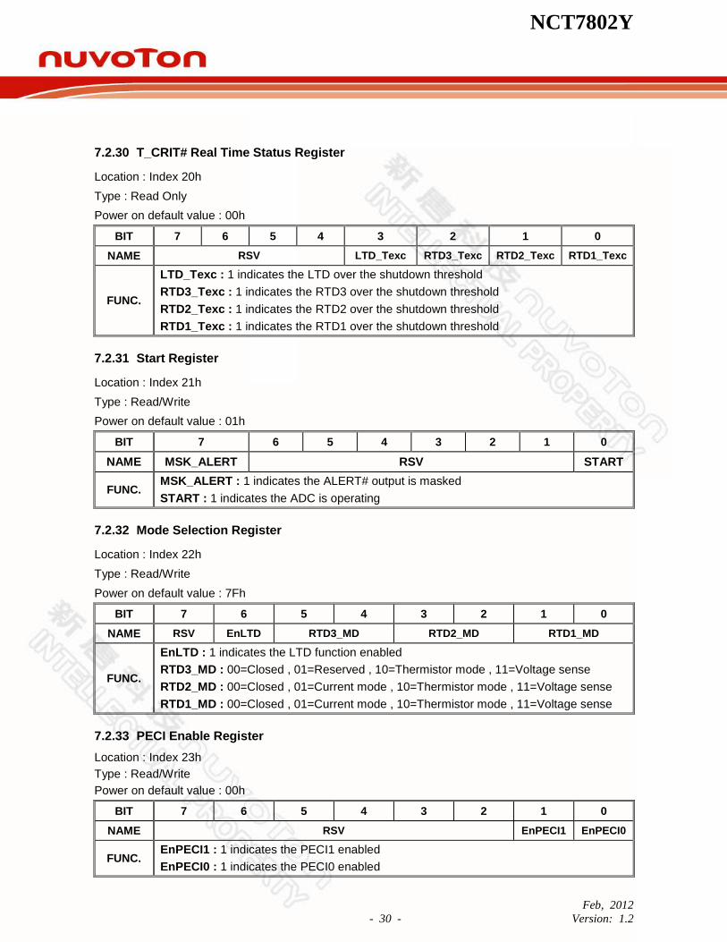
7.2.30 T_CRIT# Real Time Status Register
Location : Index 20h
Type : Read Only
Power on default value : 00h
BIT 7 6 5 4 3 2 1 0
NAME RSV LTD_Texc RTD3_Texc RTD2_Texc RTD1_Texc
FUNC.
LTD_Texc : 1 indicates the LTD over the shutdown threshold
RTD3_Texc : 1 indicates the RTD3 over the shutdown threshold
RTD2_Texc : 1 indicates the RTD2 over the shutdown threshold
RTD1_Texc : 1 indicates the RTD1 over the shutdown threshold
7.2.31 Start Register
Location : Index 21h
Type : Read/Write
Power on default value : 01h
BIT 7 6 5 4 3 2 1 0
NAME MSK_ALERT RSV START
FUNC. MSK_ALERT : 1 indicates the ALERT# output is masked
START : 1 indicates the ADC is operating
7.2.32 Mode Selection Register
Location : Index 22h
Type : Read/Write
Power on default value : 7Fh
BIT 7 6 5 4 3 2 1 0
NAME RSV EnLTD RTD3_MD RTD2_MD RTD1_MD
FUNC.
EnLTD : 1 indicates the LTD function enabled
RTD3_MD : 00=Closed , 01=Reserved , 10=Thermistor mode , 11=Voltage sense
RTD2_MD : 00=Closed , 01=Current mode , 10=Thermistor mode , 11=Voltage sense
RTD1_MD : 00=Closed , 01=Current mode , 10=Thermistor mode , 11=Voltage sense
7.2.33 PECI Enable Register
Location : Index 23h
Type : Read/Write
Power on default value : 00h
BIT 7 6 5 4 3 2 1 0
NAME RSV EnPECI1 EnPECI0
FUNC. EnPECI1 : 1 indicates the PECI1 enabled
EnPECI0 : 1 indicates the PECI0 enabled
NCT7802Y
Feb, 2012
- 31 - Version: 1.2
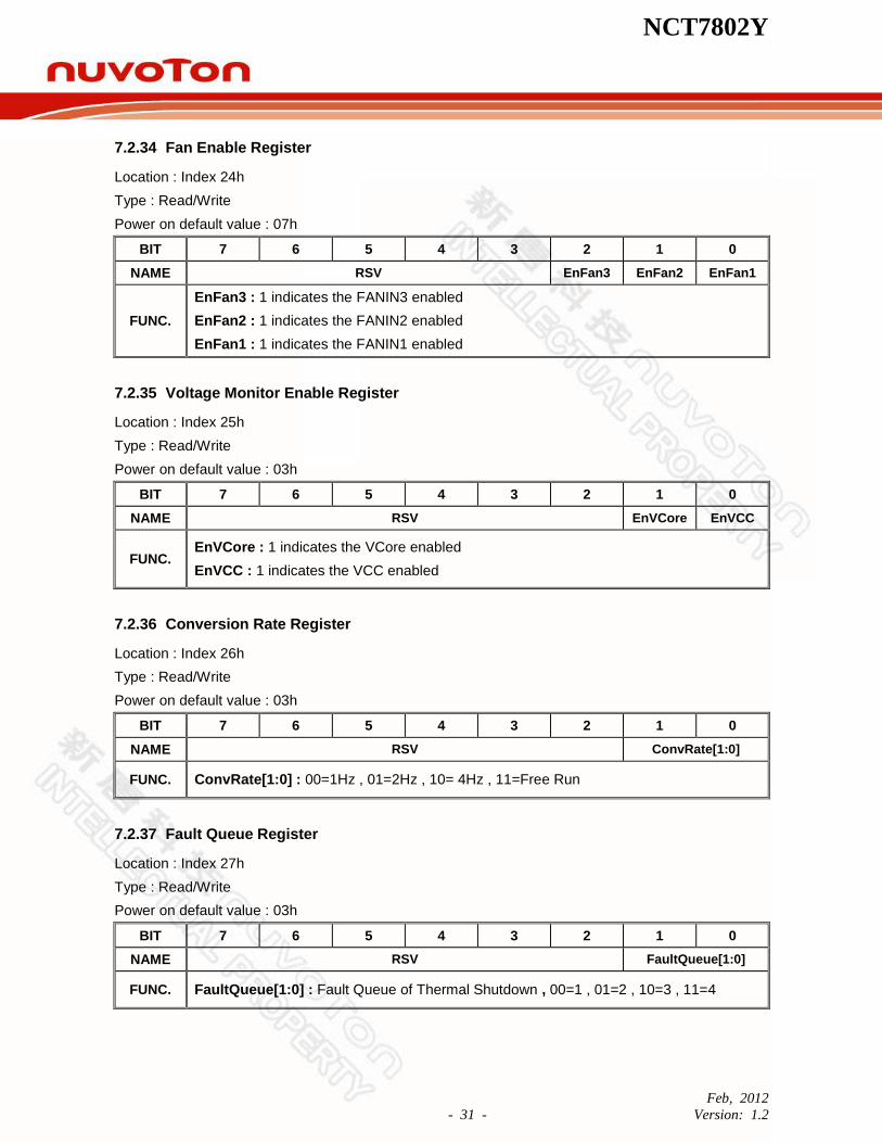
7.2.34 Fan Enable Register
Location : Index 24h
Type : Read/Write
Power on default value : 07h
BIT 7 6 5 4 3 2 1 0
NAME RSV EnFan3 EnFan2 EnFan1
FUNC.
EnFan3 : 1 indicates the FANIN3 enabled
EnFan2 : 1 indicates the FANIN2 enabled
EnFan1 : 1 indicates the FANIN1 enabled
7.2.35 Voltage Monitor Enable Register
Location : Index 25h
Type : Read/Write
Power on default value : 03h
BIT 7 6 5 4 3 2 1 0
NAME RSV EnVCore EnVCC
FUNC. EnVCore : 1 indicates the VCore enabled
EnVCC : 1 indicates the VCC enabled
7.2.36 Conversion Rate Register
Location : Index 26h
Type : Read/Write
Power on default value : 03h
BIT 7 6 5 4 3 2 1 0
NAME RSV ConvRate[1:0]
FUNC. ConvRate[1:0] : 00=1Hz , 01=2Hz , 10= 4Hz , 11=Free Run
7.2.37 Fault Queue Register
Location : Index 27h
Type : Read/Write
Power on default value : 03h
BIT 7 6 5 4 3 2 1 0
NAME RSV FaultQueue[1:0]
FUNC. FaultQueue[1:0] : Fault Queue of Thermal Shutdown , 00=1 , 01=2 , 10=3 , 11=4

NCT7802Y
Feb, 2012
- 32 - Version: 1.2
7.2.38 Alert# High Limit Link to T_CRIT# Register
Location : Index 28h
Type : Read/Write
Power on default value : 00h
BIT 7 6 5 4 3 2 1 0
NAME RSV SYS3 SYS2 SYS1
FUNC.
SYS3 : 1 indicates the External Diode3 channel high limit will be linked to T_CRIT#
SYS2 : 1 indicates the External Diode2 channel high limit will be linked to T_CRIT#
SYS1 : 1 indicates the External Diode1 channel high limit will be linked to T_CRIT#
7.2.39 Reset Time Setting Register
Location : Index 29h
Type : Read/Write
Power on default value : 04h
BIT 7 6 5 4 3 2 1 0
NAME RSV SetResetTime
FUNC. SetResetTime : 000=1ms , 001=12.5ms , 010=50ms , 011=100ms
100=200ms , 101=400ms , 110=800ms , 111=1600ms
7.2.40 Reset Limit Low Byte Register
Location : Index 2Ah
Type : Read/Write
Power on default value : EEh
BIT 7 6 5 4 3 2 1 0
NAME ResetLimit[7:0]
FUNC. ResetLimit[7:0] : Reset Limit Low Byte
7.2.41 Reset Limit High Byte Register
Location : Index 2Bh
Type : Read/Write
Power on default value : 80h
BIT 7 6 5 4 3 2 1 0
NAME ResetLimit[9:8] RSV
FUNC. ResetLimit[9:8] : Reset Limit High Byte
The Reset voltage threshold formula = Vreset-thd / 0.004
For example, the Reset voltage shreshold is 3.0V, the registers setting will be:
3.0 / 0.004 = 750, the Index[2Bh]=80h, Index[2Ah]=EEh.
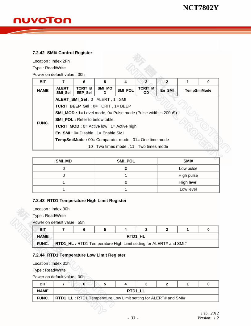
NCT7802Y
Feb, 2012
- 33 - Version: 1.2
7.2.42 SMI# Control Register
Location : Index 2Fh
Type : Read/Write
Power on default value : 00h
BIT 7 6 5 4 3 2 1 0
NAME ALERT_SMI_Sel
TCRIT_BEEP_Sel
SMI_MOD
SMI_POL TCRIT_M
OD En_SMI TempSmiMode
FUNC.
ALERT_SMI_Sel : 0= ALERT , 1= SMI
TCRIT_BEEP_Sel : 0= TCRIT , 1= BEEP
SMI_MOD : 1= Level mode, 0= Pulse mode (Pulse width is 200uS)
SMI_POL : Refer to below table.
TCRIT_MOD : 0= Active low , 1= Active high
En_SMI : 0= Disable , 1= Enable SMI
TempSmiMode : 00= Comparator mode , 01= One time mode
10= Two times mode , 11= Two times mode
SMI_MD SMI_POL SMI#
0 0 Low pulse
0 1 High pulse
1 0 High level
1 1 Low level
7.2.43 RTD1 Temperature High Limit Register
Location : Index 30h
Type : Read/Write
Power on default value : 55h
BIT 7 6 5 4 3 2 1 0
NAME RTD1_HL
FUNC. RTD1_HL : RTD1 Temperature High Limit setting for ALERT# and SMI#
7.2.44 RTD1 Temperature Low Limit Register
Location : Index 31h
Type : Read/Write
Power on default value : 00h
BIT 7 6 5 4 3 2 1 0
NAME RTD1_LL
FUNC. RTD1_LL : RTD1 Temperature Low Limit setting for ALERT# and SMI#
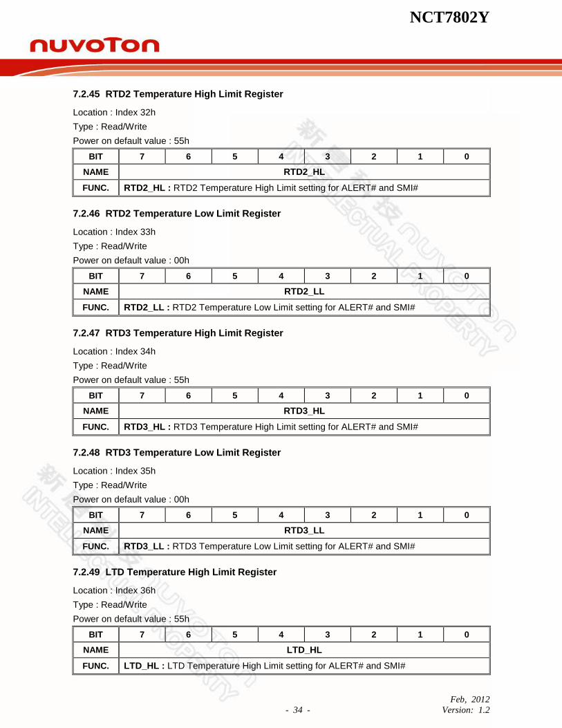
NCT7802Y
Feb, 2012
- 34 - Version: 1.2
7.2.45 RTD2 Temperature High Limit Register
Location : Index 32h
Type : Read/Write
Power on default value : 55h
BIT 7 6 5 4 3 2 1 0
NAME RTD2_HL
FUNC. RTD2_HL : RTD2 Temperature High Limit setting for ALERT# and SMI#
7.2.46 RTD2 Temperature Low Limit Register
Location : Index 33h
Type : Read/Write
Power on default value : 00h
BIT 7 6 5 4 3 2 1 0
NAME RTD2_LL
FUNC. RTD2_LL : RTD2 Temperature Low Limit setting for ALERT# and SMI#
7.2.47 RTD3 Temperature High Limit Register
Location : Index 34h
Type : Read/Write
Power on default value : 55h
BIT 7 6 5 4 3 2 1 0
NAME RTD3_HL
FUNC. RTD3_HL : RTD3 Temperature High Limit setting for ALERT# and SMI#
7.2.48 RTD3 Temperature Low Limit Register
Location : Index 35h
Type : Read/Write
Power on default value : 00h
BIT 7 6 5 4 3 2 1 0
NAME RTD3_LL
FUNC. RTD3_LL : RTD3 Temperature Low Limit setting for ALERT# and SMI#
7.2.49 LTD Temperature High Limit Register
Location : Index 36h
Type : Read/Write
Power on default value : 55h
BIT 7 6 5 4 3 2 1 0
NAME LTD_HL
FUNC. LTD_HL : LTD Temperature High Limit setting for ALERT# and SMI#
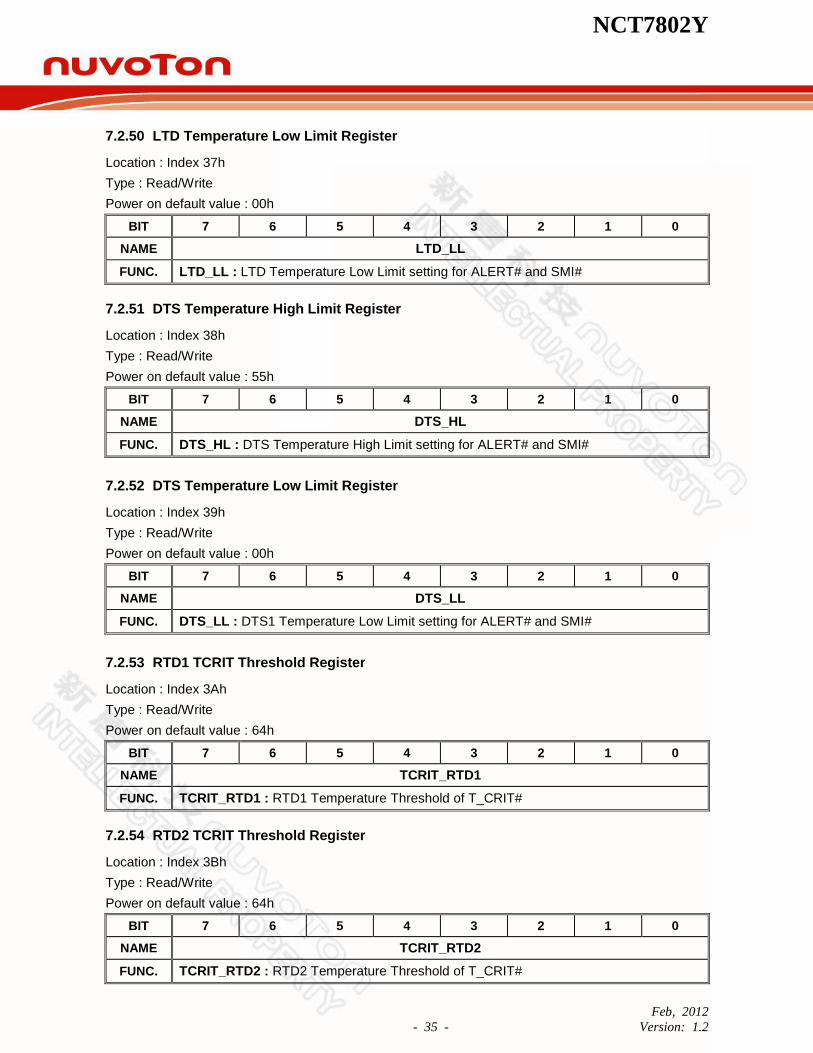
NCT7802Y
Feb, 2012
- 35 - Version: 1.2
7.2.50 LTD Temperature Low Limit Register
Location : Index 37h
Type : Read/Write
Power on default value : 00h
BIT 7 6 5 4 3 2 1 0
NAME LTD_LL
FUNC. LTD_LL : LTD Temperature Low Limit setting for ALERT# and SMI#
7.2.51 DTS Temperature High Limit Register
Location : Index 38h
Type : Read/Write
Power on default value : 55h
BIT 7 6 5 4 3 2 1 0
NAME DTS_HL
FUNC. DTS_HL : DTS Temperature High Limit setting for ALERT# and SMI#
7.2.52 DTS Temperature Low Limit Register
Location : Index 39h
Type : Read/Write
Power on default value : 00h
BIT 7 6 5 4 3 2 1 0
NAME DTS_LL
FUNC. DTS_LL : DTS1 Temperature Low Limit setting for ALERT# and SMI#
7.2.53 RTD1 TCRIT Threshold Register
Location : Index 3Ah
Type : Read/Write
Power on default value : 64h
BIT 7 6 5 4 3 2 1 0
NAME TCRIT_RTD1
FUNC. TCRIT_RTD1 : RTD1 Temperature Threshold of T_CRIT#
7.2.54 RTD2 TCRIT Threshold Register
Location : Index 3Bh
Type : Read/Write
Power on default value : 64h
BIT 7 6 5 4 3 2 1 0
NAME TCRIT_RTD2
FUNC. TCRIT_RTD2 : RTD2 Temperature Threshold of T_CRIT#
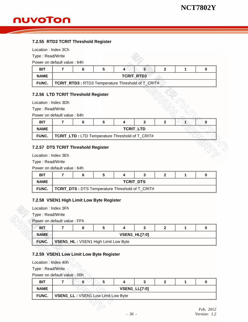
NCT7802Y
Feb, 2012
- 36 - Version: 1.2
7.2.55 RTD3 TCRIT Threshold Register
Location : Index 3Ch
Type : Read/Write
Power on default value : 64h
BIT 7 6 5 4 3 2 1 0
NAME TCRIT_RTD3
FUNC. TCRIT_RTD3 : RTD3 Temperature Threshold of T_CRIT#
7.2.56 LTD TCRIT Threshold Register
Location : Index 3Dh
Type : Read/Write
Power on default value : 64h
BIT 7 6 5 4 3 2 1 0
NAME TCRIT_LTD
FUNC. TCRIT_LTD : LTD Temperature Threshold of T_CRIT#
7.2.57 DTS TCRIT Threshold Register
Location : Index 3Eh
Type : Read/Write
Power on default value : 64h
BIT 7 6 5 4 3 2 1 0
NAME TCRIT_DTS
FUNC. TCRIT_DTS : DTS Temperature Threshold of T_CRIT#
7.2.58 VSEN1 High Limit Low Byte Register
Location : Index 3Fh
Type : Read/Write
Power on default value : FFh
BIT 7 6 5 4 3 2 1 0
NAME VSEN1_HL[7:0]
FUNC. VSEN1_HL : VSEN1 High Limit Low Byte
7.2.59 VSEN1 Low Limit Low Byte Register
Location : Index 40h
Type : Read/Write
Power on default value : 00h
BIT 7 6 5 4 3 2 1 0
NAME VSEN1_LL[7:0]
FUNC. VSEN1_LL : VSEN1 Low Limit Low Byte

NCT7802Y
Feb, 2012
- 37 - Version: 1.2
7.2.60 VSEN2 High Limit Low Byte Register
Location : Index 41h
Type : Read/Write
Power on default value : FFh
BIT 7 6 5 4 3 2 1 0
NAME VSEN2_HL[7:0]
FUNC. VSEN2_HL : VSEN2 High Limit Low Byte
7.2.61 VSEN2 Low Limit Low Byte Register
Location : Index 42h
Type : Read/Write
Power on default value : 00h
BIT 7 6 5 4 3 2 1 0
NAME VSEN2_LL[7:0]
FUNC. VSEN2_LL : VSEN2 Low Limit Low Byte
7.2.62 VSEN3 High Limit Low Byte Register
Location : Index 43h
Type : Read/Write
Power on default value : FFh
BIT 7 6 5 4 3 2 1 0
NAME VSEN3_HL[7:0]
FUNC. VSEN3_HL : VSEN3 High Limit Low Byte
7.2.63 VSEN3 Low Limit Low Byte Register
Location : Index 44h
Type : Read/Write
Power on default value : 00h
BIT 7 6 5 4 3 2 1 0
NAME VSEN3_LL[7:0]
FUNC. VSEN3_LL : VSEN3 Low Limit Low Byte
7.2.64 VCC High Limit Low Byte Register
Location : Index 45h
Type : Read/Write
Power on default value : FFh
BIT 7 6 5 4 3 2 1 0
NAME VCC_HL[7:0]
FUNC. VCC_HL : VCC High Limit Low Byte
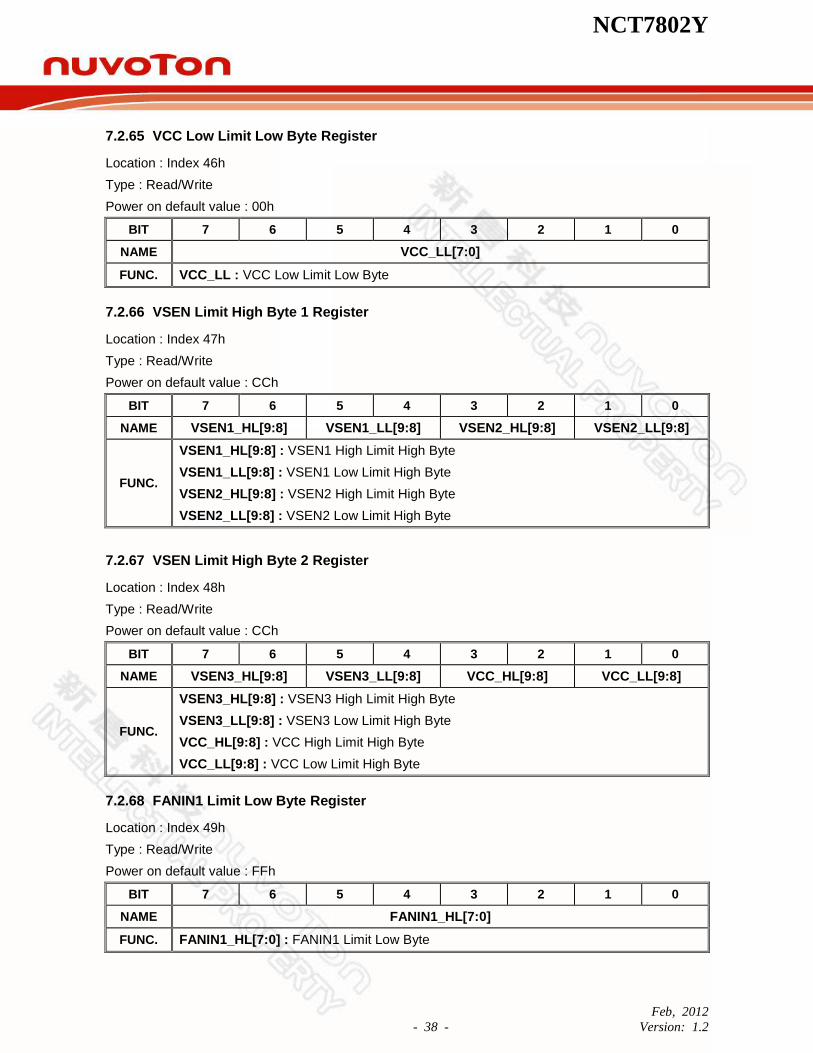
NCT7802Y
Feb, 2012
- 38 - Version: 1.2
7.2.65 VCC Low Limit Low Byte Register
Location : Index 46h
Type : Read/Write
Power on default value : 00h
BIT 7 6 5 4 3 2 1 0
NAME VCC_LL[7:0]
FUNC. VCC_LL : VCC Low Limit Low Byte
7.2.66 VSEN Limit High Byte 1 Register
Location : Index 47h
Type : Read/Write
Power on default value : CCh
BIT 7 6 5 4 3 2 1 0
NAME VSEN1_HL[9:8] VSEN1_LL[9:8] VSEN2_HL[9:8] VSEN2_LL[9:8]
FUNC.
VSEN1_HL[9:8] : VSEN1 High Limit High Byte
VSEN1_LL[9:8] : VSEN1 Low Limit High Byte
VSEN2_HL[9:8] : VSEN2 High Limit High Byte
VSEN2_LL[9:8] : VSEN2 Low Limit High Byte
7.2.67 VSEN Limit High Byte 2 Register
Location : Index 48h
Type : Read/Write
Power on default value : CCh
BIT 7 6 5 4 3 2 1 0
NAME VSEN3_HL[9:8] VSEN3_LL[9:8] VCC_HL[9:8] VCC_LL[9:8]
FUNC.
VSEN3_HL[9:8] : VSEN3 High Limit High Byte
VSEN3_LL[9:8] : VSEN3 Low Limit High Byte
VCC_HL[9:8] : VCC High Limit High Byte
VCC_LL[9:8] : VCC Low Limit High Byte
7.2.68 FANIN1 Limit Low Byte Register
Location : Index 49h
Type : Read/Write
Power on default value : FFh
BIT 7 6 5 4 3 2 1 0
NAME FANIN1_HL[7:0]
FUNC. FANIN1_HL[7:0] : FANIN1 Limit Low Byte

NCT7802Y
Feb, 2012
- 39 - Version: 1.2
7.2.69 FANIN2 Limit Low Byte Register
Location : Index 4Ah
Type : Read/Write
Power on default value : FFh
BIT 7 6 5 4 3 2 1 0
NAME FANIN2_HL[7:0]
FUNC. FANIN2_HL[7:0] : FANIN2 Limit Low Byte
7.2.70 FANIN3 Limit Low Byte Register
Location : Index 4Bh
Type : Read/Write
Power on default value : FFh
BIT 7 6 5 4 3 2 1 0
NAME FANIN3_HL[7:0]
FUNC. FANIN3_HL[7:0] : FANIN3 Limit Low Byte
7.2.71 FANIN1 Limit High Byte Register
Location : Index 4Ch
Type : Read/Write
Power on default value : F8h
BIT 7 6 5 4 3 2 1 0
NAME FANIN1_HL[12:8] RSV
FUNC. FANIN1_HL[12:8] : FANIN1 Limit High Byte
7.2.72 FANIN2 Limit High Byte Register
Location : Index 4Dh
Type : Read/Write
Power on default value : F8h
BIT 7 6 5 4 3 2 1 0
NAME FANIN2_HL[12:8] RSV
FUNC. FANIN2_HL[12:8] : FANIN2 Limit High Byte
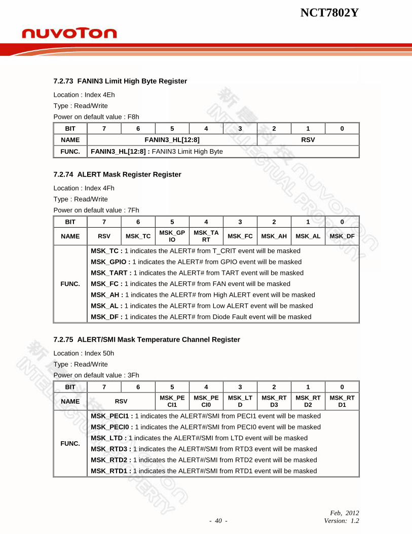
NCT7802Y
Feb, 2012
- 40 - Version: 1.2
7.2.73 FANIN3 Limit High Byte Register
Location : Index 4Eh
Type : Read/Write
Power on default value : F8h
BIT 7 6 5 4 3 2 1 0
NAME FANIN3_HL[12:8] RSV
FUNC. FANIN3_HL[12:8] : FANIN3 Limit High Byte
7.2.74 ALERT Mask Register Register
Location : Index 4Fh
Type : Read/Write
Power on default value : 7Fh
BIT 7 6 5 4 3 2 1 0
NAME RSV MSK_TC MSK_GP
IO MSK_TA
RT MSK_FC MSK_AH MSK_AL MSK_DF
FUNC.
MSK_TC : 1 indicates the ALERT# from T_CRIT event will be masked
MSK_GPIO : 1 indicates the ALERT# from GPIO event will be masked
MSK_TART : 1 indicates the ALERT# from TART event will be masked
MSK_FC : 1 indicates the ALERT# from FAN event will be masked
MSK_AH : 1 indicates the ALERT# from High ALERT event will be masked
MSK_AL : 1 indicates the ALERT# from Low ALERT event will be masked
MSK_DF : 1 indicates the ALERT# from Diode Fault event will be masked
7.2.75 ALERT/SMI Mask Temperature Channel Register
Location : Index 50h
Type : Read/Write
Power on default value : 3Fh
BIT 7 6 5 4 3 2 1 0
NAME RSV MSK_PE
CI1 MSK_PE
CI0 MSK_LT
D MSK_RT
D3 MSK_RT
D2 MSK_RT
D1
FUNC.
MSK_PECI1 : 1 indicates the ALERT#/SMI from PECI1 event will be masked
MSK_PECI0 : 1 indicates the ALERT#/SMI from PECI0 event will be masked
MSK_LTD : 1 indicates the ALERT#/SMI from LTD event will be masked
MSK_RTD3 : 1 indicates the ALERT#/SMI from RTD3 event will be masked
MSK_RTD2 : 1 indicates the ALERT#/SMI from RTD2 event will be masked
MSK_RTD1 : 1 indicates the ALERT#/SMI from RTD1 event will be masked
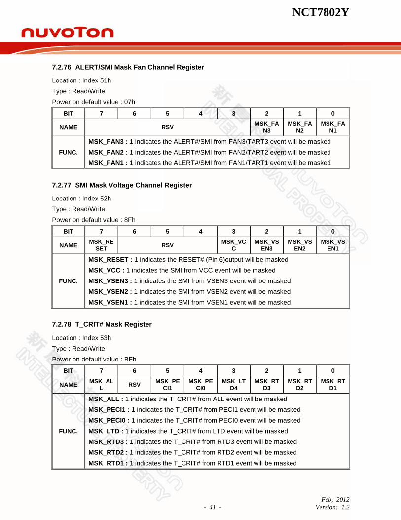
NCT7802Y
Feb, 2012
- 41 - Version: 1.2
7.2.76 ALERT/SMI Mask Fan Channel Register
Location : Index 51h
Type : Read/Write
Power on default value : 07h
BIT 7 6 5 4 3 2 1 0
NAME RSV MSK_FA
N3 MSK_FA
N2 MSK_FA
N1
FUNC.
MSK_FAN3 : 1 indicates the ALERT#/SMI from FAN3/TART3 event will be masked
MSK_FAN2 : 1 indicates the ALERT#/SMI from FAN2/TART2 event will be masked
MSK_FAN1 : 1 indicates the ALERT#/SMI from FAN1/TART1 event will be masked
7.2.77 SMI Mask Voltage Channel Register
Location : Index 52h
Type : Read/Write
Power on default value : 8Fh
BIT 7 6 5 4 3 2 1 0
NAME MSK_RE
SET RSV
MSK_VCC
MSK_VSEN3
MSK_VSEN2
MSK_VSEN1
FUNC.
MSK_RESET : 1 indicates the RESET# (Pin 6)output will be masked
MSK_VCC : 1 indicates the SMI from VCC event will be masked
MSK_VSEN3 : 1 indicates the SMI from VSEN3 event will be masked
MSK_VSEN2 : 1 indicates the SMI from VSEN2 event will be masked
MSK_VSEN1 : 1 indicates the SMI from VSEN1 event will be masked
7.2.78 T_CRIT# Mask Register
Location : Index 53h
Type : Read/Write
Power on default value : BFh
BIT 7 6 5 4 3 2 1 0
NAME MSK_AL
L RSV
MSK_PECI1
MSK_PECI0
MSK_LTD4
MSK_RTD3
MSK_RTD2
MSK_RTD1
FUNC.
MSK_ALL : 1 indicates the T_CRIT# from ALL event will be masked
MSK_PECI1 : 1 indicates the T_CRIT# from PECI1 event will be masked
MSK_PECI0 : 1 indicates the T_CRIT# from PECI0 event will be masked
MSK_LTD : 1 indicates the T_CRIT# from LTD event will be masked
MSK_RTD3 : 1 indicates the T_CRIT# from RTD3 event will be masked
MSK_RTD2 : 1 indicates the T_CRIT# from RTD2 event will be masked
MSK_RTD1 : 1 indicates the T_CRIT# from RTD1 event will be masked
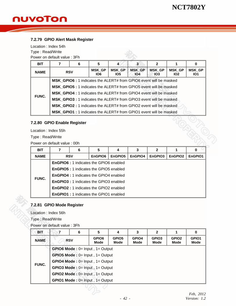
NCT7802Y
Feb, 2012
- 42 - Version: 1.2
7.2.79 GPIO Alert Mask Register
Location : Index 54h
Type : Read/Write
Power on default value : 3Fh
BIT 7 6 5 4 3 2 1 0
NAME RSV MSK_GP
IO6 MSK_GP
IO5 MSK_GP
IO4 MSK_GP
IO3 MSK_GP
IO2 MSK_GP
IO1
FUNC.
MSK_GPIO6 : 1 indicates the ALERT# from GPIO6 event will be masked
MSK_GPIO5 : 1 indicates the ALERT# from GPIO5 event will be masked
MSK_GPIO4 : 1 indicates the ALERT# from GPIO4 event will be masked
MSK_GPIO3 : 1 indicates the ALERT# from GPIO3 event will be masked
MSK_GPIO2 : 1 indicates the ALERT# from GPIO2 event will be masked
MSK_GPIO1 : 1 indicates the ALERT# from GPIO1 event will be masked
7.2.80 GPIO Enable Register
Location : Index 55h
Type : Read/Write
Power on default value : 00h
BIT 7 6 5 4 3 2 1 0
NAME RSV EnGPIO6 EnGPIO5 EnGPIO4 EnGPIO3 EnGPIO2 EnGPIO1
FUNC.
EnGPIO6 : 1 indicates the GPIO6 enabled
EnGPIO5 : 1 indicates the GPIO5 enabled
EnGPIO4 : 1 indicates the GPIO4 enabled
EnGPIO3 : 1 indicates the GPIO3 enabled
EnGPIO2 : 1 indicates the GPIO2 enabled
EnGPIO1 : 1 indicates the GPIO1 enabled
7.2.81 GPIO Mode Register
Location : Index 56h
Type : Read/Write
Power on default value : 3Fh
BIT 7 6 5 4 3 2 1 0
NAME RSV GPIO6 Mode
GPIO5 Mode
GPIO4 Mode
GPIO3 Mode
GPIO2 Mode
GPIO1 Mode
FUNC.
GPIO6 Mode : 0= Input , 1= Output
GPIO5 Mode : 0= Input , 1= Output
GPIO4 Mode : 0= Input , 1= Output
GPIO3 Mode : 0= Input , 1= Output
GPIO2 Mode : 0= Input , 1= Output
GPIO1 Mode : 0= Input , 1= Output
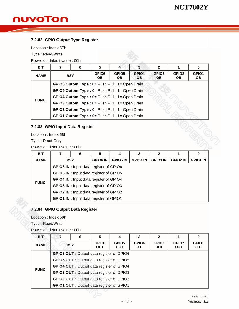
NCT7802Y
Feb, 2012
- 43 - Version: 1.2
7.2.82 GPIO Output Type Register
Location : Index 57h
Type : Read/Write
Power on default value : 00h
BIT 7 6 5 4 3 2 1 0
NAME RSV GPIO6
OB GPIO5
OB GPIO4
OB GPIO3
OB GPIO2
OB GPIO1
OB
FUNC.
GPIO6 Output Type : 0= Push Pull , 1= Open Drain
GPIO5 Output Type : 0= Push Pull , 1= Open Drain
GPIO4 Output Type : 0= Push Pull , 1= Open Drain
GPIO3 Output Type : 0= Push Pull , 1= Open Drain
GPIO2 Output Type : 0= Push Pull , 1= Open Drain
GPIO1 Output Type : 0= Push Pull , 1= Open Drain
7.2.83 GPIO Input Data Register
Location : Index 58h
Type : Read Only
Power on default value : 00h
BIT 7 6 5 4 3 2 1 0
NAME RSV GPIO6 IN GPIO5 IN GPIO4 IN GPIO3 IN GPIO2 IN GPIO1 IN
FUNC.
GPIO6 IN : Input data register of GPIO6
GPIO5 IN : Input data register of GPIO5
GPIO4 IN : Input data register of GPIO4
GPIO3 IN : Input data register of GPIO3
GPIO2 IN : Input data register of GPIO2
GPIO1 IN : Input data register of GPIO1
7.2.84 GPIO Output Data Register
Location : Index 59h
Type : Read/Write
Power on default value : 00h
BIT 7 6 5 4 3 2 1 0
NAME RSV GPIO6 OUT
GPIO5 OUT
GPIO4 OUT
GPIO3 OUT
GPIO2 OUT
GPIO1 OUT
FUNC.
GPIO6 OUT : Output data register of GPIO6
GPIO5 OUT : Output data register of GPIO5
GPIO4 OUT : Output data register of GPIO4
GPIO3 OUT : Output data register of GPIO3
GPIO2 OUT : Output data register of GPIO2
GPIO1 OUT : Output data register of GPIO1

NCT7802Y
Feb, 2012
- 44 - Version: 1.2
7.2.85 BEEP Voltage Channel Enable Register
Location : Index 5Ah
Type : Read/Write
Power on default value : 00h
BIT 7 6 5 4 3 2 1 0
NAME RSV EnBP_R
ESET EnBP_V
CC EnBP_V
SEN3 EnBP_V
SEN2 EnBP_V
SEN1
FUNC.
EnBP_RESET : 1 indicates the BEEP is enabled for RESET event
EnBP_VCC : 1 indicates the BEEP is enabled for VCC event
EnBP_VSEN3 : 1 indicates the BEEP is enabled for VSEN3 event
EnBP_VSEN2 : 1 indicates the BEEP is enabled for VSEN2 event
EnBP_VSEN1 : 1 indicates the BEEP is enabled for VSEN1 event
7.2.86 BEEP Fan Channel Enable Register
Location : Index 5Bh
Type : Read/Write
Power on default value : 00h
BIT 7 6 5 4 3 2 1 0
NAME RSV EnBP_FAN3 EnBP_FAN2 EnBP_FAN1
FUNC.
EnBP_FAN3 : 1 indicates the BEEP is enabled for FAN3 event
EnBP_FAN2 : 1 indicates the BEEP is enabled for FAN2 event
EnBP_FAN1 : 1 indicates the BEEP is enabled for FAN1 event
7.2.87 BEEP Temperature Channel Enable Register
Location : Index 5Ch
Type : Read/Write
Power on default value : 00h
BIT 7 6 5 4 3 2 1 0
NAME RSV EnBP_P
ECI1 EnBP_P
ECI0 EnBP_L
TD ENBP_R
TD3 EnBP_R
TD2 EnBP_R
TD1
FUNC.
EnBP_PECI1 : 1 indicates the BEEP is enabled for PECI1 event
EnBP_PECI0 : 1 indicates the BEEP is enabled for PECI0 event
EnBP_LTD : 1 indicates the BEEP is enabled for LTD event
EnBP_RTD3 : 1 indicates the BEEP is enabled for RTD3 event
EnBP_RTD2 : 1 indicates the BEEP is enabled for RTD2 event
EnBP_RTD1 : 1 indicates the BEEP is enabled for RTD1 event
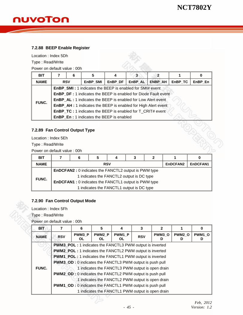
NCT7802Y
Feb, 2012
- 45 - Version: 1.2
7.2.88 BEEP Enable Register
Location : Index 5Dh
Type : Read/Write
Power on default value : 00h
BIT 7 6 5 4 3 2 1 0
NAME RSV EnBP_SMI EnBP_DF EnBP_AL ENBP_AH EnBP_TC EnBP_En
FUNC.
EnBP_SMI : 1 indicates the BEEP is enabled for SMI# event
EnBP_DF : 1 indicates the BEEP is enabled for Diode Fault event
EnBP_AL : 1 indicates the BEEP is enabled for Low Alert event
EnBP_AH : 1 indicates the BEEP is enabled for High Alert event
EnBP_TC : 1 indicates the BEEP is enabled for T_CRIT# event
EnBP_En : 1 indicates the BEEP is enabled
7.2.89 Fan Control Output Type
Location : Index 5Eh
Type : Read/Write
Power on default value : 00h
BIT 7 6 5 4 3 2 1 0
NAME RSV EnDCFAN2 EnDCFAN1
FUNC.
EnDCFAN2 : 0 indicates the FANCTL2 output is PWM type
1 indicates the FANCTL2 output is DC type
EnDCFAN1 : 0 indicates the FANCTL1 output is PWM type
1 indicates the FANCTL1 output is DC type
7.2.90 Fan Control Output Mode
Location : Index 5Fh
Type : Read/Write
Power on default value : 00h
BIT 7 6 5 4 3 2 1 0
NAME RSV PWM3_P
OL PWM2_P
OL PWM1_P
OL RSV
PWM3_OD
PWM2_OD
PWM1_OD
FUNC.
PWM3_POL : 1 indicates the FANCTL3 PWM output is inverted
PWM2_POL : 1 indicates the FANCTL2 PWM output is inverted
PWM1_POL : 1 indicates the FANCTL1 PWM output is inverted
PWM3_OD : 0 indicates the FANCTL3 PWM output is push pull
1 indicates the FANCTL3 PWM output is open drain
PWM2_OD : 0 indicates the FANCTL2 PWM output is push pull
1 indicates the FANCTL2 PWM output is open drain
PWM1_OD : 0 indicates the FANCTL1 PWM output is push pull
1 indicates the FANCTL1 PWM output is open drain

NCT7802Y
Feb, 2012
- 46 - Version: 1.2
7.2.91 Fan Control 1 Output Value
Location : Index 60h
Type : Read/Write for Manual mode , Read only for SMART FANTM
IV control
Power on default value : 7FHEX.
BIT 7 6 5 4 3 2 1 0
NAME FANDuty1
FUNC. FANDuty1 : FANCTL1 output value
7.2.92 Fan Control 2 Output Value
Location : Index 61h
Type : Read/Write for Manual mode , Read only for SMART FANTM
IV control
Power on default value : 7FHEX.
BIT 7 6 5 4 3 2 1 0
NAME FANDuty2
FUNC. FANDuty2 : FANCTL2 output value
7.2.93 Fan Control 3 Output Value
Location : Index 62h
Type : Read/Write for Manual mode , Read only for SMART FANTM
IV control
Power on default value : 7FHEX.
BIT 7 6 5 4 3 2 1 0
NAME FANDuty3
FUNC. FANDuty3 : FANCTL3 output value
7.2.94 Close-Loop Fan Control RPM mode Register and Configure Register of PECI Error (CRPE)
Location : Index 63h
Type : Read/Write
Power on default value : 00h
BIT 7 6 5 4 3 2 1 0
NAME TwoDimension RPM_HIGH_EN PECIERR
FUNC.
TwoDimension : Close_Loop Fan Control Enable
Bit7 : 1 indicated the FAN3 group enables Close-Loop Fan Control RPM mode
Bit6 : 1 indicated the FAN2 group enables Close-Loop Fan Control RPM mode
Bit5 : 1 indicated the FAN1 group enables Close-Loop Fan Control RPM mode
RPM_HIGH_EN : Changing default unit of all RPM setting from 50 RPMs to 100 RPMs.
It benefits to control ultra high RPM fan
Bit4 : 1 indicated the FAN3 group support ultra high RPM fan
Bit3 : 1 indicated the FAN2 group support ultra high RPM fan
Bit2 : 1 indicated the FAN1 group support ultra high RPM fan
PECIERR : Refer the table 7-1 PECI Error Condition Table to fan output value
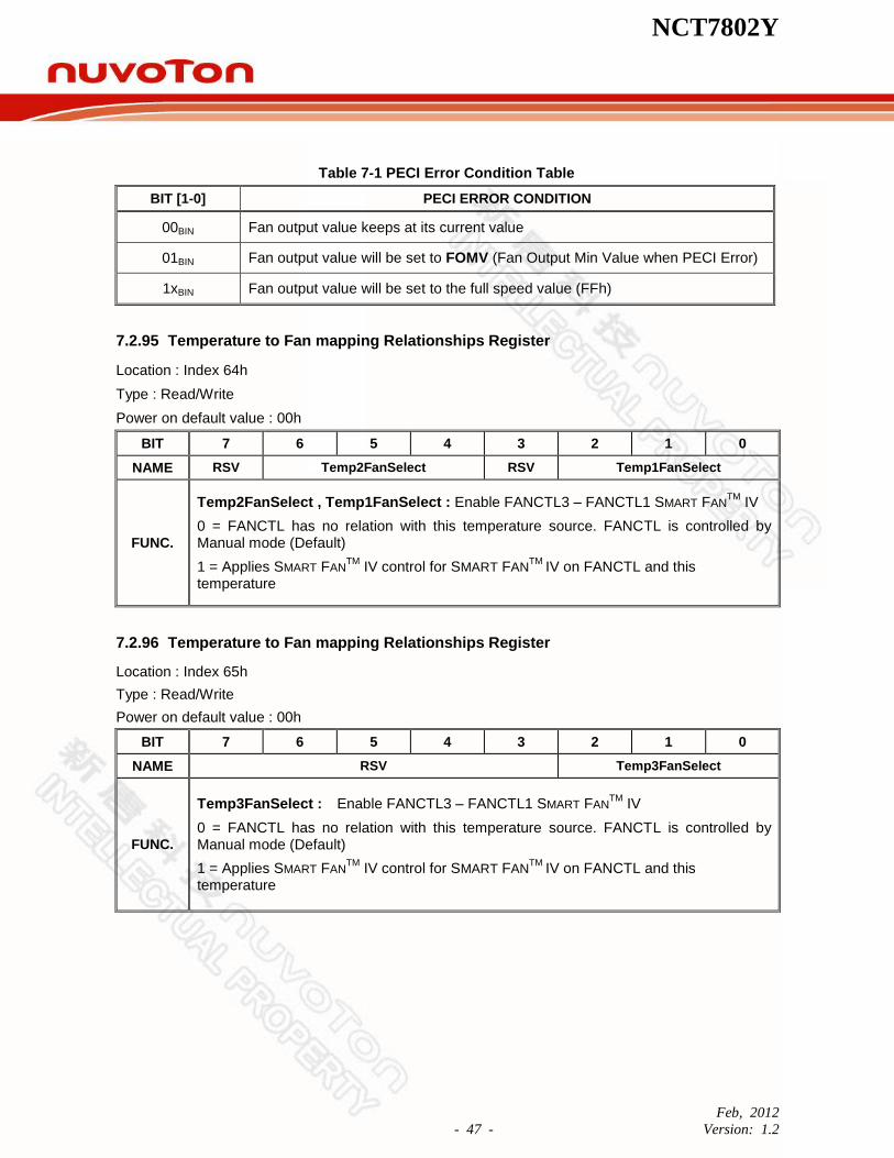
NCT7802Y
Feb, 2012
- 47 - Version: 1.2
Table 7-1 PECI Error Condition Table
BIT [1-0] PECI ERROR CONDITION
00BIN Fan output value keeps at its current value
01BIN Fan output value will be set to FOMV (Fan Output Min Value when PECI Error)
1xBIN Fan output value will be set to the full speed value (FFh)
7.2.95 Temperature to Fan mapping Relationships Register
Location : Index 64h
Type : Read/Write
Power on default value : 00h
BIT 7 6 5 4 3 2 1 0
NAME RSV Temp2FanSelect RSV Temp1FanSelect
FUNC.
Temp2FanSelect , Temp1FanSelect : Enable FANCTL3 – FANCTL1 SMART FANTM
IV
0 = FANCTL has no relation with this temperature source. FANCTL is controlled by Manual mode (Default)
1 = Applies SMART FANTM
IV control for SMART FANTM
IV on FANCTL and this temperature
7.2.96 Temperature to Fan mapping Relationships Register
Location : Index 65h
Type : Read/Write
Power on default value : 00h
BIT 7 6 5 4 3 2 1 0
NAME RSV Temp3FanSelect
FUNC.
Temp3FanSelect : Enable FANCTL3 – FANCTL1 SMART FANTM
IV
0 = FANCTL has no relation with this temperature source. FANCTL is controlled by Manual mode (Default)
1 = Applies SMART FANTM
IV control for SMART FANTM
IV on FANCTL and this temperature
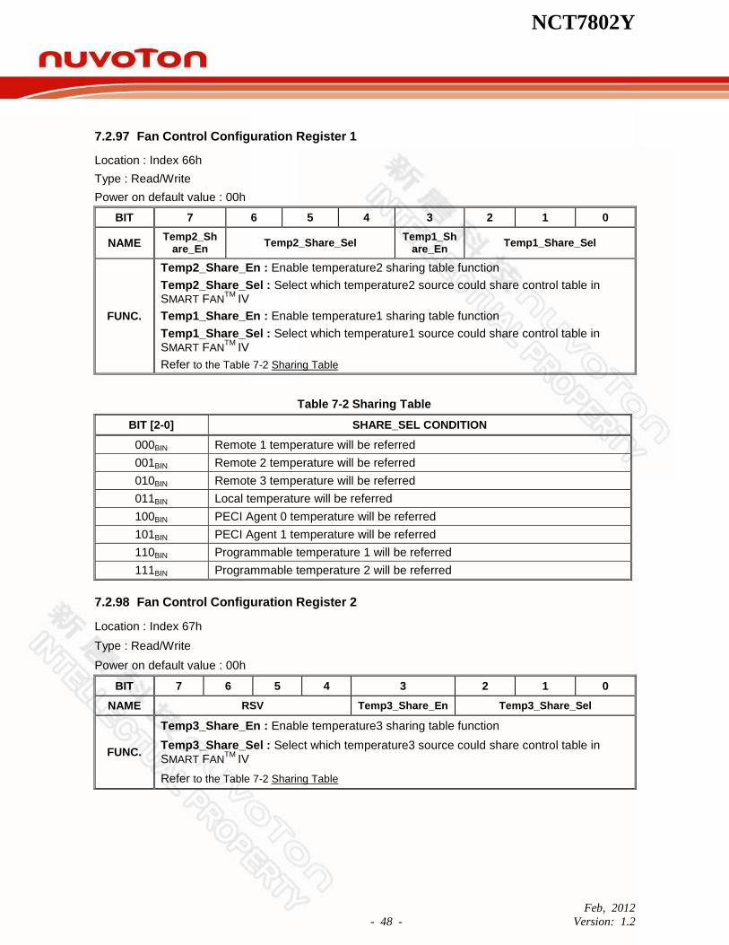
NCT7802Y
Feb, 2012
- 48 - Version: 1.2
7.2.97 Fan Control Configuration Register 1
Location : Index 66h
Type : Read/Write
Power on default value : 00h
BIT 7 6 5 4 3 2 1 0
NAME Temp2_Sh
are_En Temp2_Share_Sel
Temp1_Share_En
Temp1_Share_Sel
FUNC.
Temp2_Share_En : Enable temperature2 sharing table function
Temp2_Share_Sel : Select which temperature2 source could share control table in SMART FAN
TM IV
Temp1_Share_En : Enable temperature1 sharing table function
Temp1_Share_Sel : Select which temperature1 source could share control table in SMART FAN
TM IV
Refer to the Table 7-2 Sharing Table
Table 7-2 Sharing Table
BIT [2-0] SHARE_SEL CONDITION
000BIN Remote 1 temperature will be referred
001BIN Remote 2 temperature will be referred
010BIN Remote 3 temperature will be referred
011BIN Local temperature will be referred
100BIN PECI Agent 0 temperature will be referred
101BIN PECI Agent 1 temperature will be referred
110BIN Programmable temperature 1 will be referred
111BIN Programmable temperature 2 will be referred
7.2.98 Fan Control Configuration Register 2
Location : Index 67h
Type : Read/Write
Power on default value : 00h
BIT 7 6 5 4 3 2 1 0
NAME RSV Temp3_Share_En Temp3_Share_Sel
FUNC.
Temp3_Share_En : Enable temperature3 sharing table function
Temp3_Share_Sel : Select which temperature3 source could share control table in SMART FAN
TM IV
Refer to the Table 7-2 Sharing Table
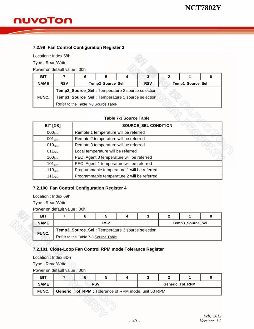
NCT7802Y
Feb, 2012
- 49 - Version: 1.2
7.2.99 Fan Control Configuration Register 3
Location : Index 68h
Type : Read/Write
Power on default value : 00h
BIT 7 6 5 4 3 2 1 0
NAME RSV Temp2_Source_Sel RSV Temp1_Source_Sel
FUNC.
Temp2_Source_Sel : Temperature 2 source selection
Temp1_Source_Sel : Temperature 1 source selection
Refer to the Table 7-3 Source Table
Table 7-3 Source Table
BIT [2-0] SOURCE_SEL CONDITION
000BIN Remote 1 temperature will be referred
001BIN Remote 2 temperature will be referred
010BIN Remote 3 temperature will be referred
011BIN Local temperature will be referred
100BIN PECI Agent 0 temperature will be referred
101BIN PECI Agent 1 temperature will be referred
110BIN Programmable temperature 1 will be referred
111BIN Programmable temperature 2 will be referred
7.2.100 Fan Control Configuration Register 4
Location : Index 69h
Type : Read/Write
Power on default value : 00h
BIT 7 6 5 4 3 2 1 0
NAME RSV Temp3_Source_Sel
FUNC. Temp3_Source_Sel : Temperature 3 source selection
Refer to the Table 7-3 Source Table
7.2.101 Close-Loop Fan Control RPM mode Tolerance Register
Location : Index 6Dh
Type : Read/Write
Power on default value : 00h
BIT 7 6 5 4 3 2 1 0
NAME RSV Generic_Tol_RPM
FUNC. Generic_Tol_RPM : Tolerance of RPM mode, unit 50 RPM
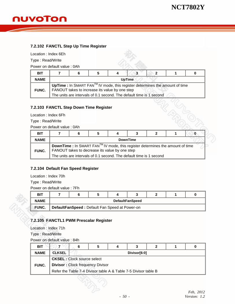
NCT7802Y
Feb, 2012
- 50 - Version: 1.2
7.2.102 FANCTL Step Up Time Register
Location : Index 6Eh
Type : Read/Write
Power on default value : 0Ah
BIT 7 6 5 4 3 2 1 0
NAME UpTime
FUNC.
UpTime : In SMART FANTM
IV mode, this register determines the amount of time FANOUT takes to increase its value by one step
The units are intervals of 0.1 second. The default time is 1 second
7.2.103 FANCTL Step Down Time Register
Location : Index 6Fh
Type : Read/Write
Power on default value : 0Ah
BIT 7 6 5 4 3 2 1 0
NAME DownTime
FUNC.
DownTime : In SMART FANTM
IV mode, this register determines the amount of time FANOUT takes to decrease its value by one step
The units are intervals of 0.1 second. The default time is 1 second
7.2.104 Default Fan Speed Register
Location : Index 70h
Type : Read/Write
Power on default value : 7Fh
BIT 7 6 5 4 3 2 1 0
NAME DefaultFanSpeed
FUNC. DefaultFanSpeed : Default Fan Speed at Power-on
7.2.105 FANCTL1 PWM Prescalar Register
Location : Index 71h
Type : Read/Write
Power on default value : 84h
BIT 7 6 5 4 3 2 1 0
NAME CLKSEL Divisor[6:0]
FUNC.
CKSEL : Clock source select
Divisor : Clock frequency Divisor
Refer the Table 7-4 Divisor table A & Table 7-5 Divisor table B

NCT7802Y
Feb, 2012
- 51 - Version: 1.2
The clock source selected by CKSEL will be divided by the divisor and used as a fan PWM output frequency.
If CKSEL equals 1, then the output clock is simply equal to 125/ (Divisor [6:0]+1) KHz
MappedDivisor depends on Divisor [6:0] and is described in the table below.
Table 7-4 Divisor Table A (CKSEL=1)
DIVISOR[6:0] MAPPED DIVISOR
OUTPUT FREQUENCY
DIVISOR[6:0] MAPPED DIVISOR
OUTPUT FREQUENCY
0000000 1 125KHz
RSV
0000001 2 62.5KHz
0000010 3 41.6KHz
0000011 4 31.2KHz
0000100 5 25KHz 0001111 16 7.8KHz
0000101 6 20.8KHz 0011111 32 3.9KHz
0000110 7 17.8KHz 0111111 64 1.9KHz
0000111 8 15.6KHz 1111111 128 976Hz
If CKSEL equals 0, then the output clock is simply equal to 1000/ Mapped Divisor Hz
MappedDivisor depends on Divisor [3:0] and is described in the table below.
Table 7-5 Divisor Table B (CKSEL=0)
DIVISOR[3:0] MAPPED DIVISOR
OUTPUT FREQUENCY
DIVISOR[3:0] MAPPED DIVISOR
OUTPUT FREQUENCY
0000 1 1000Hz 1000 12 83Hz
0001 2 500Hz 1001 16 62.5Hz
0010 3 333Hz 1010 32 31.25Hz
0011 4 250Hz 1011 64 15.6Hz
0100 5 200Hz 1100 128 7.8Hz
0101 6 166Hz 1101 256 3.9Hz
0110 7 142Hz 1110 512 1.9Hz
0111 8 125Hz 1111 1024 0.97Hz
7.2.106 FANCTL2 PWM Prescalar Register
Location : Index 72h
Type : Read/Write
Power on default value : 84h
BIT 7 6 5 4 3 2 1 0
NAME CLKSEL Divisor[6:0]
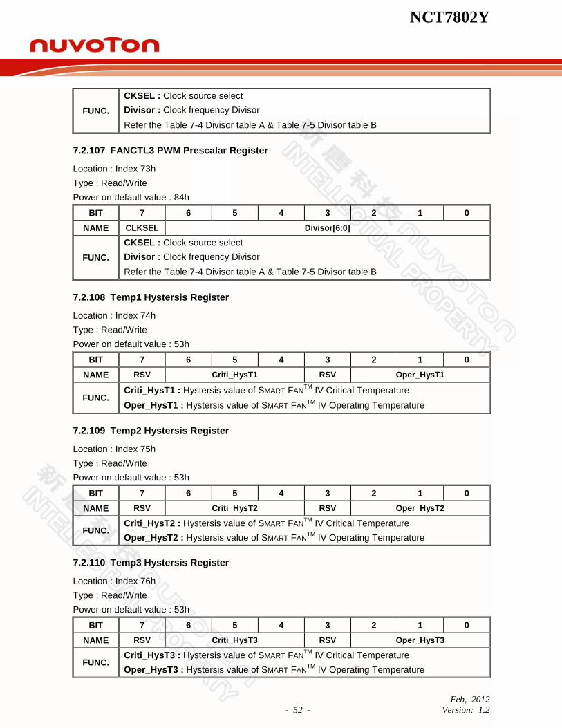
NCT7802Y
Feb, 2012
- 52 - Version: 1.2
FUNC.
CKSEL : Clock source select
Divisor : Clock frequency Divisor
Refer the Table 7-4 Divisor table A & Table 7-5 Divisor table B
7.2.107 FANCTL3 PWM Prescalar Register
Location : Index 73h
Type : Read/Write
Power on default value : 84h
BIT 7 6 5 4 3 2 1 0
NAME CLKSEL Divisor[6:0]
FUNC.
CKSEL : Clock source select
Divisor : Clock frequency Divisor
Refer the Table 7-4 Divisor table A & Table 7-5 Divisor table B
7.2.108 Temp1 Hystersis Register
Location : Index 74h
Type : Read/Write
Power on default value : 53h
BIT 7 6 5 4 3 2 1 0
NAME RSV Criti_HysT1 RSV Oper_HysT1
FUNC. Criti_HysT1 : Hystersis value of SMART FAN
TM IV Critical Temperature
Oper_HysT1 : Hystersis value of SMART FANTM
IV Operating Temperature
7.2.109 Temp2 Hystersis Register
Location : Index 75h
Type : Read/Write
Power on default value : 53h
BIT 7 6 5 4 3 2 1 0
NAME RSV Criti_HysT2 RSV Oper_HysT2
FUNC. Criti_HysT2 : Hystersis value of SMART FAN
TM IV Critical Temperature
Oper_HysT2 : Hystersis value of SMART FANTM
IV Operating Temperature
7.2.110 Temp3 Hystersis Register
Location : Index 76h
Type : Read/Write
Power on default value : 53h
BIT 7 6 5 4 3 2 1 0
NAME RSV Criti_HysT3 RSV Oper_HysT3
FUNC. Criti_HysT3 : Hystersis value of SMART FAN
TM IV Critical Temperature
Oper_HysT3 : Hystersis value of SMART FANTM
IV Operating Temperature
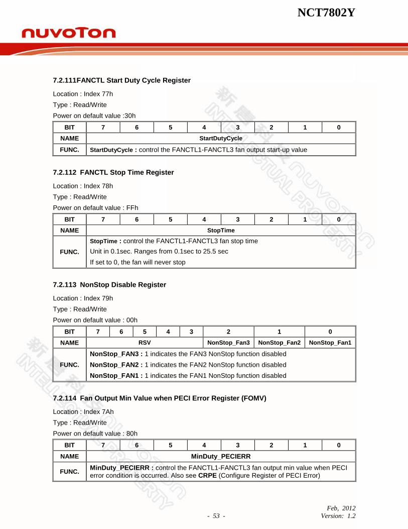
NCT7802Y
Feb, 2012
- 53 - Version: 1.2
7.2.111 FANCTL Start Duty Cycle Register
Location : Index 77h
Type : Read/Write
Power on default value :30h
BIT 7 6 5 4 3 2 1 0
NAME StartDutyCycle
FUNC. StartDutyCycle : control the FANCTL1-FANCTL3 fan output start-up value
7.2.112 FANCTL Stop Time Register
Location : Index 78h
Type : Read/Write
Power on default value : FFh
BIT 7 6 5 4 3 2 1 0
NAME StopTime
FUNC.
StopTime : control the FANCTL1-FANCTL3 fan stop time
Unit in 0.1sec. Ranges from 0.1sec to 25.5 sec
If set to 0, the fan will never stop
7.2.113 NonStop Disable Register
Location : Index 79h
Type : Read/Write
Power on default value : 00h
BIT 7 6 5 4 3 2 1 0
NAME RSV NonStop_Fan3 NonStop_Fan2 NonStop_Fan1
FUNC.
NonStop_FAN3 : 1 indicates the FAN3 NonStop function disabled
NonStop_FAN2 : 1 indicates the FAN2 NonStop function disabled
NonStop_FAN1 : 1 indicates the FAN1 NonStop function disabled
7.2.114 Fan Output Min Value when PECI Error Register (FOMV)
Location : Index 7Ah
Type : Read/Write
Power on default value : 80h
BIT 7 6 5 4 3 2 1 0
NAME MinDuty_PECIERR
FUNC. MinDuty_PECIERR : control the FANCTL1-FANCTL3 fan output min value when PECI error condition is occurred. Also see CRPE (Configure Register of PECI Error)

NCT7802Y
Feb, 2012
- 54 - Version: 1.2
7.2.115 Table 1 X-axis Transition Point 1 Register
Location : Index 80h
Type : Read/Write
Power on default value : 19h
BIT 7 6 5 4 3 2 1 0
NAME Temp1Table_TR1
FUNC. Temp1Table_TR1 : Temperature point 1 of SMART FANTM
IV table 1
7.2.116 Table 1 X-axis Transition Point 2 Register
Location : Index 81h
Type : Read/Write
Power on default value : 23h
BIT 7 6 5 4 3 2 1 0
NAME Temp1Table_TR2
FUNC. Temp1Table_TR2 : Temperature point 2 of SMART FANTM
IV table 1
7.2.117 Table 1 X-axis Transition Point 3 Register
Location : Index 82h
Type : Read/Write
Power on default value : 2Dh
BIT 7 6 5 4 3 2 1 0
NAME Temp1Table_TR3
FUNC. Temp1Table_TR3 : Temperature point 3 of SMART FANTM
IV table 1
7.2.118 Table 1 X-axis Transition Point 4 Register
Location : Index 83h
Type : Read/Write
Power on default value : 37h
BIT 7 6 5 4 3 2 1 0
NAME Temp1Table_TR4
FUNC. Temp1Table_TR4 : Temperature point 4 of SMART FANTM
IV table 1
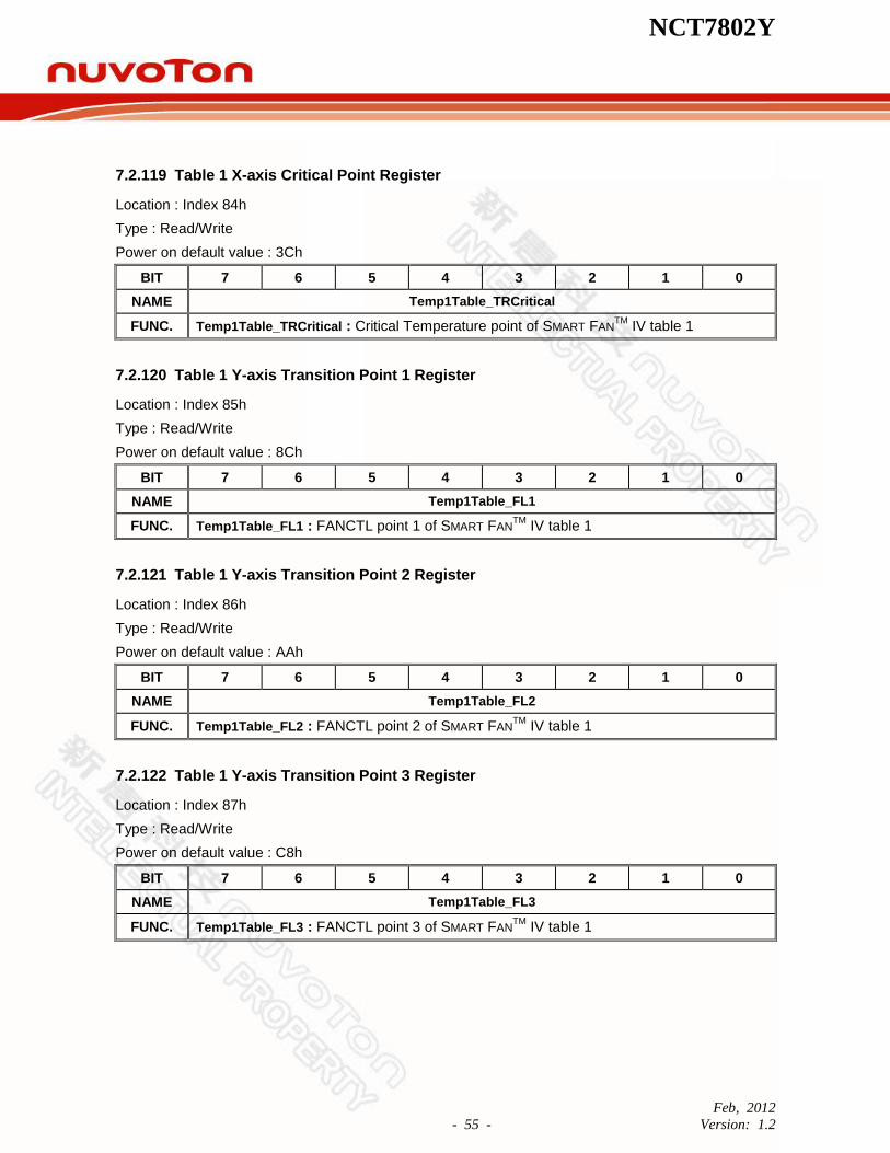
NCT7802Y
Feb, 2012
- 55 - Version: 1.2
7.2.119 Table 1 X-axis Critical Point Register
Location : Index 84h
Type : Read/Write
Power on default value : 3Ch
BIT 7 6 5 4 3 2 1 0
NAME Temp1Table_TRCritical
FUNC. Temp1Table_TRCritical : Critical Temperature point of SMART FANTM
IV table 1
7.2.120 Table 1 Y-axis Transition Point 1 Register
Location : Index 85h
Type : Read/Write
Power on default value : 8Ch
BIT 7 6 5 4 3 2 1 0
NAME Temp1Table_FL1
FUNC. Temp1Table_FL1 : FANCTL point 1 of SMART FANTM
IV table 1
7.2.121 Table 1 Y-axis Transition Point 2 Register
Location : Index 86h
Type : Read/Write
Power on default value : AAh
BIT 7 6 5 4 3 2 1 0
NAME Temp1Table_FL2
FUNC. Temp1Table_FL2 : FANCTL point 2 of SMART FANTM
IV table 1
7.2.122 Table 1 Y-axis Transition Point 3 Register
Location : Index 87h
Type : Read/Write
Power on default value : C8h
BIT 7 6 5 4 3 2 1 0
NAME Temp1Table_FL3
FUNC. Temp1Table_FL3 : FANCTL point 3 of SMART FANTM
IV table 1

NCT7802Y
Feb, 2012
- 56 - Version: 1.2
7.2.123 Table 1 Y-axis Transition Point 4 Register
Location : Index 88h
Type : Read/Write
Power on default value : E6h
BIT 7 6 5 4 3 2 1 0
NAME Temp1Table_FL4
FUNC. Temp1Table_FL4 : FANCTL point 4 of SMART FANTM
IV table 1
7.2.124 Table 2 X-axis Transition Point 1 Register
Location : Index 90h
Type : Read/Write
Power on default value : 19h
BIT 7 6 5 4 3 2 1 0
NAME Temp2Table_TR1
FUNC. Temp2Table_TR1 : Temperature point 1 of SMART FANTM
IV table 2
7.2.125 Table 2 X-axis Transition Point 2 Register
Location : Index 91h
Type : Read/Write
Power on default value : 23h
BIT 7 6 5 4 3 2 1 0
NAME Temp2Table_TR2
FUNC. Temp2Table_TR2 : Temperature point 2 of SMART FANTM
IV table 2
7.2.126 Table 2 X-axis Transition Point 3 Register
Location : Index 92h
Type : Read/Write
Power on default value : 2Dh
BIT 7 6 5 4 3 2 1 0
NAME Temp2Table_TR3
FUNC. Temp2Table_TR3 : Temperature point 3 of SMART FANTM
IV table 2

NCT7802Y
Feb, 2012
- 57 - Version: 1.2
7.2.127 Table 2 X-axis Transition Point 4 Register
Location : Index 93h
Type : Read/Write
Power on default value : 37h
BIT 7 6 5 4 3 2 1 0
NAME Temp2Table_TR4
FUNC. Temp2Table_TR4 : Temperature point 4 of SMART FANTM
IV table 2
7.2.128 Table 2 X-axis Critical Point Register
Location : Index 94h
Type : Read/Write
Power on default value : 3Ch
BIT 7 6 5 4 3 2 1 0
NAME Temp2Table_TRCritical
FUNC. Temp2Table_TRCritical : Critical Temperature point of SMART FANTM
IV table 2
7.2.129 Table 2 Y-axis Transition Point 1 Register
Location : Index 95h
Type : Read/Write
Power on default value : 8Ch
BIT 7 6 5 4 3 2 1 0
NAME Temp2Table_FL1
FUNC. Temp2Table_FL1 : FANCTL point 1 of SMART FANTM
IV table 2
7.2.130 Table 2 Y-axis Transition Point 2 Register
Location : Index 96h
Type : Read/Write
Power on default value : AAh
BIT 7 6 5 4 3 2 1 0
NAME Temp2Table_FL2
FUNC. Temp2Table_FL2 : FANCTL point 2 of SMART FANTM
IV table 2
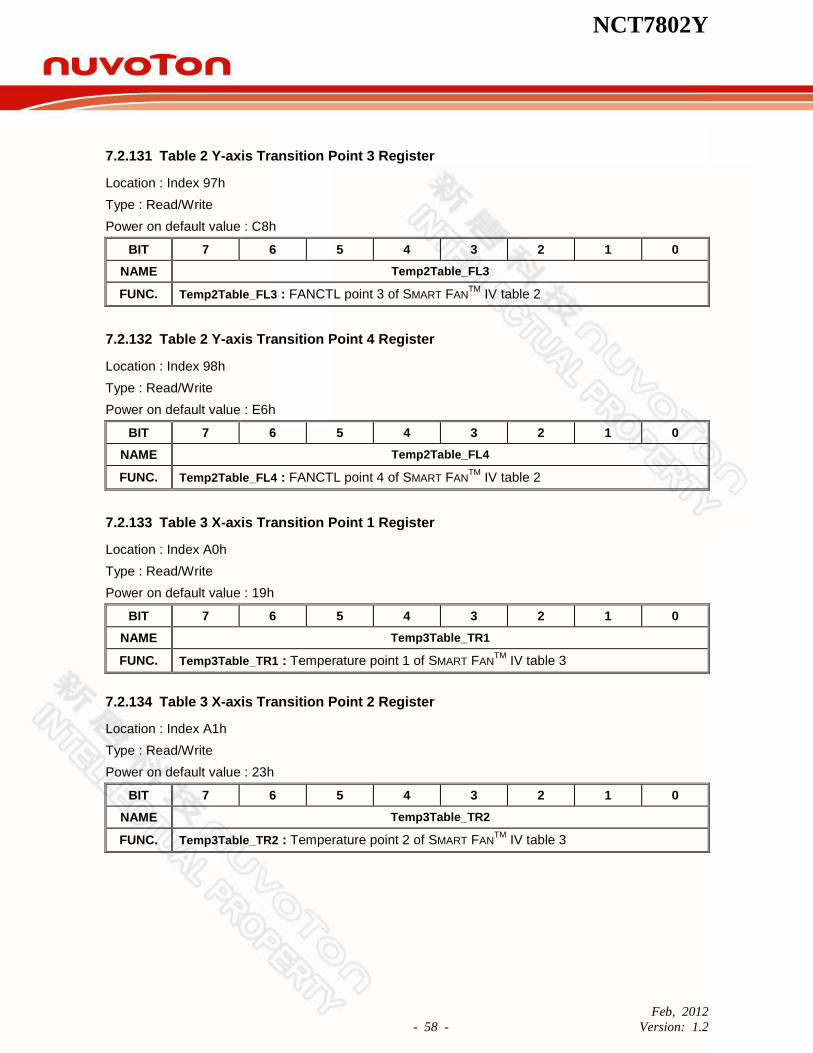
NCT7802Y
Feb, 2012
- 58 - Version: 1.2
7.2.131 Table 2 Y-axis Transition Point 3 Register
Location : Index 97h
Type : Read/Write
Power on default value : C8h
BIT 7 6 5 4 3 2 1 0
NAME Temp2Table_FL3
FUNC. Temp2Table_FL3 : FANCTL point 3 of SMART FANTM
IV table 2
7.2.132 Table 2 Y-axis Transition Point 4 Register
Location : Index 98h
Type : Read/Write
Power on default value : E6h
BIT 7 6 5 4 3 2 1 0
NAME Temp2Table_FL4
FUNC. Temp2Table_FL4 : FANCTL point 4 of SMART FANTM
IV table 2
7.2.133 Table 3 X-axis Transition Point 1 Register
Location : Index A0h
Type : Read/Write
Power on default value : 19h
BIT 7 6 5 4 3 2 1 0
NAME Temp3Table_TR1
FUNC. Temp3Table_TR1 : Temperature point 1 of SMART FANTM
IV table 3
7.2.134 Table 3 X-axis Transition Point 2 Register
Location : Index A1h
Type : Read/Write
Power on default value : 23h
BIT 7 6 5 4 3 2 1 0
NAME Temp3Table_TR2
FUNC. Temp3Table_TR2 : Temperature point 2 of SMART FANTM
IV table 3
NCT7802Y
Feb, 2012
- 59 - Version: 1.2
7.2.135 Table 3 X-axis Transition Point 3 Register
Location : Index A2h
Type : Read/Write
Power on default value : 2Dh
BIT 7 6 5 4 3 2 1 0
NAME Temp3Table_TR3
FUNC. Temp3Table_TR3 : Temperature point 3 of SMART FANTM
IV table 3
7.2.136 Table 3 X-axis Transition Point 4 Register
Location : Index A3h
Type : Read/Write
Power on default value : 37h
BIT 7 6 5 4 3 2 1 0
NAME Temp3Table_TR4
FUNC. Temp3Table_TR4 : Temperature point 4 of SMART FANTM
IV table 3
7.2.137 Table 3 X-axis Critical Point Register
Location : Index A4h
Type : Read/Write
Power on default value : 3Ch
BIT 7 6 5 4 3 2 1 0
NAME Temp3Table_TRCritical
FUNC. Temp3Table_TRCritical : Critical Temperature point of SMART FANTM
IV table 3
7.2.138 Table 3 Y-axis Transition Point 1 Register
Location : Index A5h
Type : Read/Write
Power on default value : 8Ch
BIT 7 6 5 4 3 2 1 0
NAME Temp3Table_FL1
FUNC. Temp3Table_FL1 : FANCTL point 1 of SMART FANTM
IV table 3

NCT7802Y
Feb, 2012
- 60 - Version: 1.2
7.2.139 Table 3 Y-axis Transition Point 2 Register
Location : Index A6h
Type : Read/Write
Power on default value : AAh
BIT 7 6 5 4 3 2 1 0
NAME Temp3Table_FL2
FUNC. Temp3Table_FL2 : FANCTL point 2 of SMART FANTM
IV table 3
7.2.140 Table 3 Y-axis Transition Point 3 Register
Location : Index A7h
Type : Read/Write
Power on default value : C8h
BIT 7 6 5 4 3 2 1 0
NAME Temp3Table_FL3
FUNC. Temp3Table_FL3 : FANCTL point 3 of SMART FANTM
IV table 3
7.2.141 Table 3 Y-axis Transition Point 4 Register
Location : Index A8h
Type : Read/Write
Power on default value : E6h
BIT 7 6 5 4 3 2 1 0
NAME Temp3Table_FL4
FUNC. Temp3Table_FL4 : FANCTL point 4 of SMART FANTM
IV table 3
7.2.142 TD1 Offset Register
Location : Index C1h
Type : Read/Write
Power on default value : 3Dh
BIT 7 6 5 4 3 2 1 0
NAME RSV Offset_TD1
FUNC. Offset_TD1 : TD1 function offset register
NCT7802Y
Feb, 2012
- 61 - Version: 1.2
7.2.143 TD2 Offset Register
Location : Index C2h
Type : Read/Write
Power on default value : 3Dh
BIT 7 6 5 4 3 2 1 0
NAME RSV Offset_TD2
FUNC. Offset_TD2 : TD2 function offset register
7.2.144 TR1 Offset Register
Location : Index C4h
Type : Read/Write
Power on default value : 00h
BIT 7 6 5 4 3 2 1 0
NAME RSV Offset_TR1
FUNC. Offset_TR1 : TR1 function offset register
7.2.145 TR2 Offset Register
Location : Index C5h
Type : Read/Write
Power on default value : 00h
BIT 7 6 5 4 3 2 1 0
NAME RSV Offset_TR2
FUNC. Offset_TR2 : TR2 function offset register
7.2.146 TR3 Offset Register
Location : Index C6h
Type : Read/Write
Power on default value : 00h
BIT 7 6 5 4 3 2 1 0
NAME RSV Offset_TR3
FUNC. Offset_TR3 : TR3 function offset register
NCT7802Y
Feb, 2012
- 62 - Version: 1.2
7.2.147 Digital Filter Level Select Register
Location : Index CBh
Type : Read/Write
Power on default value : 00h
BIT 7 6 5 4 3 2 1 0
NAME LDT RT3 RT2 RT1
FUNC.
00 : No filter selected. (Default)
01: Filter Level 1 selected.
10: Filter Level 2 selected.
11: Filter Level 3 selected.
Higher level will slow down the temperature sensor response.
7.2.148 Programmable Temperature 1 Register
Location : Index E3h
Type : Read/Write
Power on default value : 00h
BIT 7 6 5 4 3 2 1 0
NAME PGM_TEMP1[7:0]
FUNC. PGM_TEMP1[7:0] : Programmable Temperature 1
7.2.149 Programmable Temperature 2 Register
Location : Index E4h
Type : Read/Write
Power on default value : 00h
BIT 7 6 5 4 3 2 1 0
NAME PGM_TEMP2[7:0]
FUNC. PGM_TEMP2[7:0] : Programmable Temperature 2
7.2.150 Software Reset Register
Location : Index FCh
Type : Write Only
BIT 7 6 5 4 3 2 1 0
NAME INIT RSV
FUNC. INIT : Write 1 to reset the NCT7802Y
NCT7802Y
Feb, 2012
- 63 - Version: 1.2
7.2.151 Vendor ID Register
Location : Index FDh
Type : Ready Only
Power on default value : 50h
BIT 7 6 5 4 3 2 1 0
NAME VendorID
FUNC. VendorID: Vendor ID of NCT7802Y
7.2.152 Chip ID Register
Location : Index FEh
Type : Ready Only
Power on default value : C3h
BIT 7 6 5 4 3 2 1 0
NAME ChipID
FUNC. ChipID: Chip ID of NCT7802Y
7.2.153 Version ID Register
Location : Index FFh
Type : Ready Only
Power on default value : 2xh
BIT 7 6 5 4 3 2 1 0
NAME VersionID
FUNC. VersionID: Versin ID of NCT7802Y, the value is 2xh (x=0,1,2…)

NCT7802Y
Feb, 2012
- 64 - Version: 1.2
7.3 BANK 1 REGISTER MAP
Idx Register Name Att Df 7 6 5 4 3 2 1 0
0 Bank Select R/W 00 RSV BKSEL
1 PECI Control Reg-1 RW 10 PECI_En RSV Manual_E
n Routine_En
2 PECI Control Reg-2 RW 00 RSV TN_Extend[1:0] RSV
3 PECI Control Reg-3 RW 00 RSV En_Agt[1:0] RSV Dmn1_Agt[3:0]
4 Report Temp Style 1 RW 00 RSV Clamp RSV RtDmn_Agt[1:0] RtHigher
5 Address content for manual command
RW 00 Addr
6 Write Length for manual
command RW 00 Write_Length
7 Read Length for manual
command RW 00 Read_Length
8 Command Code for manual command
RW 00 Command_Code
9 Agent0 Base Temperature
RW 00 RSV Tbase0[6:0]
0A Agent1 Base Temperature
RW 00 RSV Tbase1[6:0]
0B Generic write in data 1 to
client RW 00 WrData_1
0C Generic write in data 2 to
client RW 00 WrData_2
0D Generic write in data 3 to
client RW 00 WrData_3
0E Generic write in data 4 to
client RW 00 WrData_4
0F Generic write in data 5 to
client RW 00 WrData_5
10 Generic write in data 6 to
client RW 00 WrData_6
11 Generic write in data 7 to
client RW 00 WrData_7
12 Generic write in data 8 to
client RW 00 WrData_8
13 Generic write in data 9 to
client RW 00 WrData_9
14 Generic write in data 10
to client RW 00 WrData_10
15 Generic write in data 11
to client RW 00 WrData_11
16 Generic write in data 12
to client RW 00 WrData_12
17 Agt0_D0 Relative Temp
(HB) RO F8 RTH_Agt0_D0
18 Agt0_D0 Relative Temp
(LB) RO 80 RTL_Agt0_D0
19 Agt0_D1 Relative Temp
(HB) RO F8 RTH_Agt0_D1
1A Agt0_D1 Relative Temp
(LB) RO 80 RTL_Agt0_D1
1B Agt1_D0 Relative Temp
(HB) RO F8 RTH_Agt1_D0
1C Agt1_D0 Relative Temp
(LB) RO 80 RTL_Agt1_D0
1D Agt1_D1 Relative Temp
(HB) RO F8 RTH_Agt1_D1
1E Agt1_D1 Relative Temp
(LB) RO 80 RTL_Agt1_D1
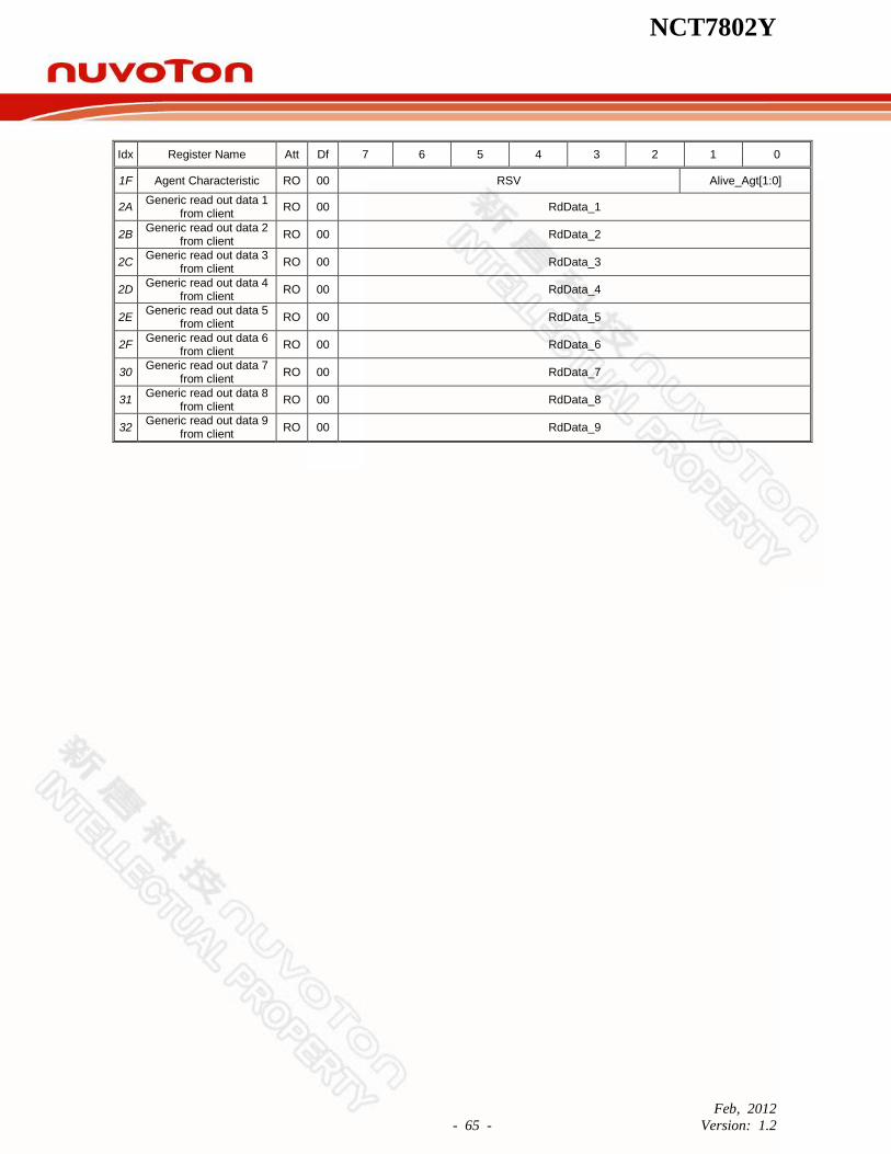
NCT7802Y
Feb, 2012
- 65 - Version: 1.2
Idx Register Name Att Df 7 6 5 4 3 2 1 0
1F Agent Characteristic RO 00 RSV Alive_Agt[1:0]
2A Generic read out data 1
from client RO 00 RdData_1
2B Generic read out data 2
from client RO 00 RdData_2
2C Generic read out data 3
from client RO 00 RdData_3
2D Generic read out data 4
from client RO 00 RdData_4
2E Generic read out data 5
from client RO 00 RdData_5
2F Generic read out data 6
from client RO 00 RdData_6
30 Generic read out data 7
from client RO 00 RdData_7
31 Generic read out data 8
from client RO 00 RdData_8
32 Generic read out data 9
from client RO 00 RdData_9

NCT7802Y
Feb, 2012
- 66 - Version: 1.2
7.4 BANK 1 REGISTER DETAIL
7.4.1 PECI Control Register 1
Location : Index 01h
Type : Read/Write
Power on default value : 10h
BIT READ / WRITE DESCRIPTION
7 R / W Enable PECI Function (PECI_En)
6~2 R / W Reserved
1 R / W Enable PECI Manual Command Function (Manual_En)
0 R / W Enable PECI GetTemp Routine Function (Routine_En)
7.4.2 PECI Control Register 2
Location : Index 02h
Type : Read/Write
Power on default value : 00h
BIT READ / WRITE DESCRIPTION
7~6 R / W Reserved
5 R / W
TN_Extend[1:0]
Adjust Transaction Rate
00BIN = 1.5 MHz
01BIN = 750 KHz
10BIN = 375 KHz
11BIN = 187.5 KHz
4 R / W
3 ~ 0 R / W Reserved
7.4.3 PECI Control Register 3
Location : Index 03h
Type : Read/Write
Power on default value : 00h
BIT READ / WRITE DESCRIPTION
7 ~ 6 R / W Reserved
5 R / W En_Agt[1:0]
PECI host to process related agents enable or disable agent
PECI host to process related agents enable or disable agent0 4 R / W
3 ~ 2 R / W Reserved
1 R / W Dmn1_Agt[1:0]
Indicate which agent with domain1
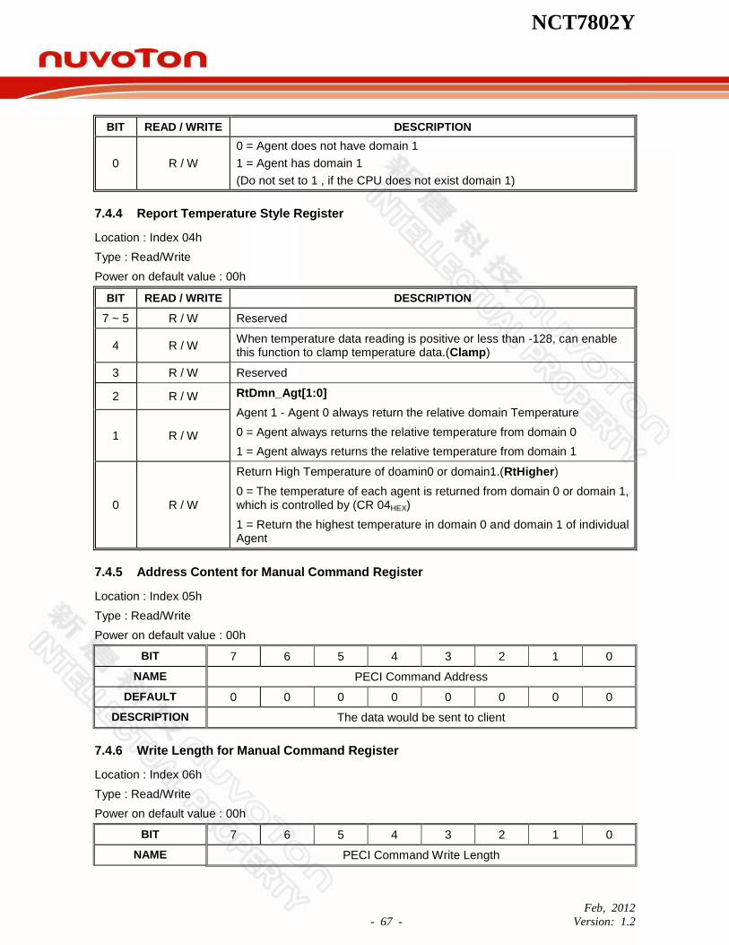
NCT7802Y
Feb, 2012
- 67 - Version: 1.2
BIT READ / WRITE DESCRIPTION
0 R / W
0 = Agent does not have domain 1
1 = Agent has domain 1
(Do not set to 1 , if the CPU does not exist domain 1)
7.4.4 Report Temperature Style Register
Location : Index 04h
Type : Read/Write
Power on default value : 00h
BIT READ / WRITE DESCRIPTION
7 ~ 5 R / W Reserved
4 R / W When temperature data reading is positive or less than -128, can enable this function to clamp temperature data.(Clamp)
3 R / W Reserved
2 R / W RtDmn_Agt[1:0]
Agent 1 - Agent 0 always return the relative domain Temperature
0 = Agent always returns the relative temperature from domain 0
1 = Agent always returns the relative temperature from domain 1
1 R / W
0 R / W
Return High Temperature of doamin0 or domain1.(RtHigher)
0 = The temperature of each agent is returned from domain 0 or domain 1, which is controlled by (CR 04HEX)
1 = Return the highest temperature in domain 0 and domain 1 of individual Agent
7.4.5 Address Content for Manual Command Register
Location : Index 05h
Type : Read/Write
Power on default value : 00h
BIT 7 6 5 4 3 2 1 0
NAME PECI Command Address
DEFAULT 0 0 0 0 0 0 0 0
DESCRIPTION The data would be sent to client
7.4.6 Write Length for Manual Command Register
Location : Index 06h
Type : Read/Write
Power on default value : 00h
BIT 7 6 5 4 3 2 1 0
NAME PECI Command Write Length
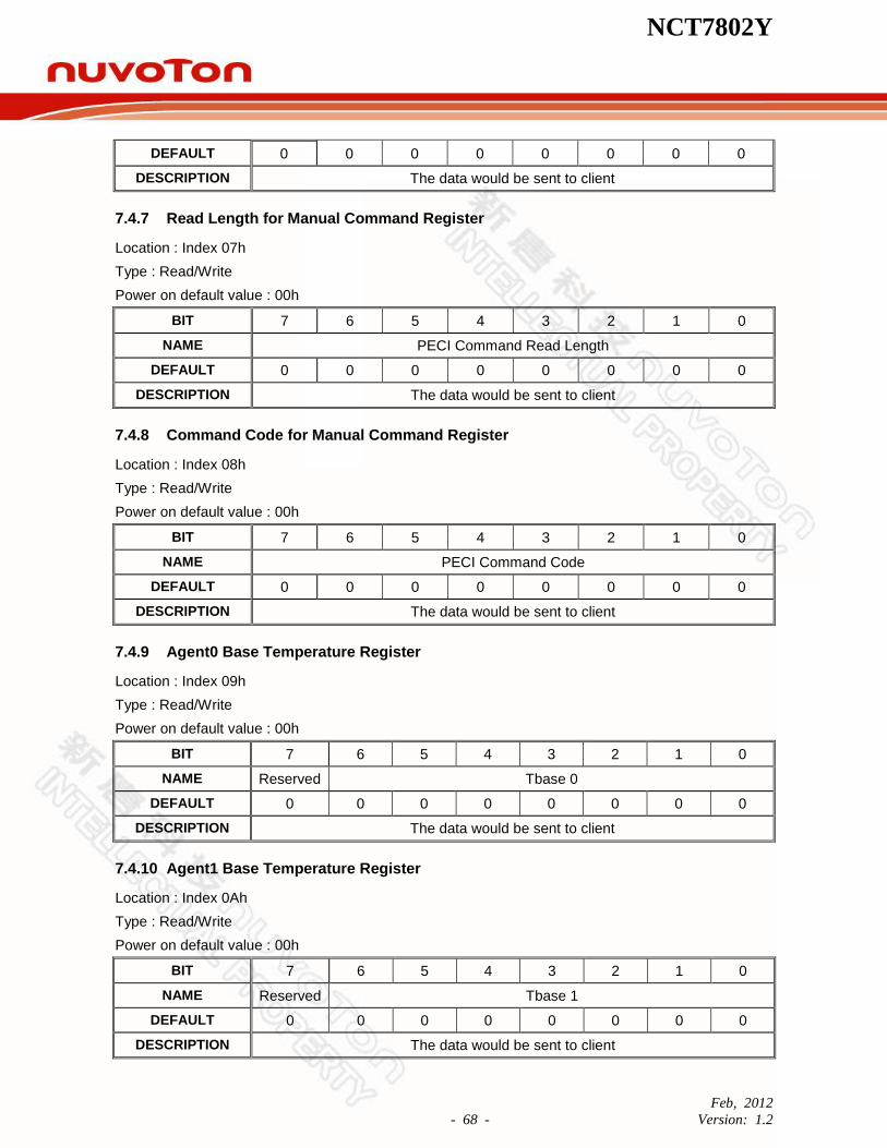
NCT7802Y
Feb, 2012
- 68 - Version: 1.2
DEFAULT 0 0 0 0 0 0 0 0
DESCRIPTION The data would be sent to client
7.4.7 Read Length for Manual Command Register
Location : Index 07h
Type : Read/Write
Power on default value : 00h
BIT 7 6 5 4 3 2 1 0
NAME PECI Command Read Length
DEFAULT 0 0 0 0 0 0 0 0
DESCRIPTION The data would be sent to client
7.4.8 Command Code for Manual Command Register
Location : Index 08h
Type : Read/Write
Power on default value : 00h
BIT 7 6 5 4 3 2 1 0
NAME PECI Command Code
DEFAULT 0 0 0 0 0 0 0 0
DESCRIPTION The data would be sent to client
7.4.9 Agent0 Base Temperature Register
Location : Index 09h
Type : Read/Write
Power on default value : 00h
BIT 7 6 5 4 3 2 1 0
NAME Reserved Tbase 0
DEFAULT 0 0 0 0 0 0 0 0
DESCRIPTION The data would be sent to client
7.4.10 Agent1 Base Temperature Register
Location : Index 0Ah
Type : Read/Write
Power on default value : 00h
BIT 7 6 5 4 3 2 1 0
NAME Reserved Tbase 1
DEFAULT 0 0 0 0 0 0 0 0
DESCRIPTION The data would be sent to client

NCT7802Y
Feb, 2012
- 69 - Version: 1.2
7.4.11 Generic Write in Data 1 to Client Register
Location : Index 0Bh
Type : Read/Write
Power on default value : 00h
BIT 7 6 5 4 3 2 1 0
NAME PECI Write Data 1
DEFAULT 0 0 0 0 0 0 0 0
DESCRIPTION The data would be sent to client
7.4.12 Generic Write in Data 2 to Client Register
Location : Index 0Ch
Type : Read/Write
Power on default value : 00h
BIT 7 6 5 4 3 2 1 0
NAME PECI Write Data 2
DEFAULT 0 0 0 0 0 0 0 0
DESCRIPTION The data would be sent to client
7.4.13 Generic Write in Data 3 to Client Register
Location : Index 0Dh
Type : Read/Write
Power on default value : 00h
BIT 7 6 5 4 3 2 1 0
NAME PECI Write Data 3
DEFAULT 0 0 0 0 0 0 0 0
DESCRIPTION The data would be sent to client
7.4.14 Generic Write in Data 4 to Client Register
Location : Index 0Eh
Type : Read/Write
Power on default value : 00h
BIT 7 6 5 4 3 2 1 0
NAME PECI Write Data 4
DEFAULT 0 0 0 0 0 0 0 0
DESCRIPTION The data would be sent to client

NCT7802Y
Feb, 2012
- 70 - Version: 1.2
7.4.15 Generic Write in Data 5 to Client Register
Location : Index 0Fh
Type : Read/Write
Power on default value : 00h
BIT 7 6 5 4 3 2 1 0
NAME PECI Write Data 5
DEFAULT 0 0 0 0 0 0 0 0
DESCRIPTION The data would be sent to client
7.4.16 Generic Write in Data 6 to Client Register
Location : Index 10h
Type : Read/Write
Power on default value : 00h
BIT 7 6 5 4 3 2 1 0
NAME PECI Write Data 6
DEFAULT 0 0 0 0 0 0 0 0
DESCRIPTION The data would be sent to client
7.4.17 Generic Write in Data 7 to Client Register
Location : Index 11h
Type : Read/Write
Power on default value : 00h
BIT 7 6 5 4 3 2 1 0
NAME PECI Write Data 7
DEFAULT 0 0 0 0 0 0 0 0
DESCRIPTION The data would be sent to client
7.4.18 Generic Write in Data 8 to Client Register
Location : Index 12h
Type : Read/Write
Power on default value : 00h
BIT 7 6 5 4 3 2 1 0
NAME PECI Write Data 8
DEFAULT 0 0 0 0 0 0 0 0
DESCRIPTION The data would be sent to client

NCT7802Y
Feb, 2012
- 71 - Version: 1.2
7.4.19 Generic Write in Data 9 to Client Register
Location : Index 13h
Type : Read/Write
Power on default value : 00h
BIT 7 6 5 4 3 2 1 0
NAME PECI Write Data 9
DEFAULT 0 0 0 0 0 0 0 0
DESCRIPTION The data would be sent to client
7.4.20 Generic Write in Data 10 to Client Register
Location : Index 14h
Type : Read/Write
Power on default value : 00h
BIT 7 6 5 4 3 2 1 0
NAME PECI Write Data 10
DEFAULT 0 0 0 0 0 0 0 0
DESCRIPTION The data would be sent to client
7.4.21 Generic Write in Data 11 to Client Register
Location : Index 15h
Type : Read/Write
Power on default value : 00h
BIT 7 6 5 4 3 2 1 0
NAME PECI Write Data 11
DEFAULT 0 0 0 0 0 0 0 0
DESCRIPTION The data would be sent to client
7.4.22 Generic Write in Data 12 to Client Register
Location : Index 16h
Type : Read/Write
Power on default value : 00h
BIT 7 6 5 4 3 2 1 0
NAME PECI Write Data 12
DEFAULT 0 0 0 0 0 0 0 0
DESCRIPTION The data would be sent to client

NCT7802Y
Feb, 2012
- 72 - Version: 1.2
7.4.23 Agent Relative Temperature Register
Location : Index 17h ~ 1Eh
Type : Read Only
Power on default value : F880h
These registers return the raw data retrieved from PECI GetTemp(). The data may be the error code (range: 8000H~81FFH) or relative temperatures to process the defined Tbase. The error code will only be update in ARTR and absolute Temperature will not be updated when the error code is received. If the RtHigher mechanism is activated, the normal temperature will always be returned first. In case both 2 domains return errors, the return priority will be Overflow Error > Underflow Error > Missing Diode > General Error. The reset value is 8001HEX, in that PECI is defaulted to be off. In PECI, 8001HEX means the diode is missing.
INDEX 17-1E DESCRIPTION
17h[15:8],18h[7:0] Domain0 Relative Temperature Agent0 [15:0]
19h[15:8],1Ah[7:0] Domain1 Relative Temperature Agent0 [15:0]
1Bh[15:8],1Ch[7:0] Domain0 Relative Temperature Agent1 [15:0]
1Dh[15:8],1Eh[7:0] Domain1 Relative Temperature Agent1 [15:0]
GetTemp() PECI Temperature format
BIT DESCRIPTION
15 Sign Bit. (Sign) In PECI Protocol, this bit should always be 1 to represent a negative temperature.
14-6 The integer part of the relative temperature. (Temperature[8:0])
5 TEMP_2. 0.5℃ unit.
4 TEMP_4. 0.25℃ unit.
3 TEMP_8. 0.125℃ unit.
2 TEMP_16. 0.0625℃ unit.
1 TEMP_32. 0.03125℃ unit.
0 TEMP_64. 0.015625℃ unit.
GetTemp() Response Definition
RESPONSE MEANING
General Sensor Error (GSE)
Thermal scan did not complete in time. Retry is appropriate.
0x0000 Processor is running at its maximum temperature or is currently being reset.
All other data
Valid temperature reading, reported as a negative offset from the TCC activation temperature.
The valide temperature reading is referred to GetTemp() PECI Temperature format

NCT7802Y
Feb, 2012
- 73 - Version: 1.2
ERROR CODE
DESCRIPTION HOST OPERATION
8000HEX General Sensor Error No further processing.
8001HEX Sensing Device Missing
8002HEX Operational, but the temperature is lower than the sensor operation range.
Compulsorily write 0℃ back to the temperature readouts.
8003HEX Operational, but the temperature is higher than the sensor operation range.
Compulsorily write 127℃ back to the temperature readouts.
8004HEX ~
81FFHEX Reserved No further operation.
7.4.24 Agent Characteristic Register
Location : Index 1Fh
Type : Read Only
Power on default value : 00h
BIT 7 6 5 4 3 2 1 0
NAME RSV PECI Alive Agent
DEFAULT 0 0 0 0 0 0 0 0
BIT DESCRIPTION
7~2 Reserved
1 1: agent1 is able to respond to Ping() command. Agent alive
0: agent1 isn‟t able to respond to Ping() command. Agent is not alive
0 1: agent0 is able to respond to Ping() command. Agent alive
0: agent0 isn‟t able to respond to Ping() command. Agent is not alive
7.4.25 Generic Read Out Data 1 from Client Register
Location : Index 2Ah
Type : Read Only
Power on default value : 00h
BIT 7 6 5 4 3 2 1 0
NAME PECI Read Data 1
DEFAULT 0 0 0 0 0 0 0 0
DESCRIPTION The data would be got from client
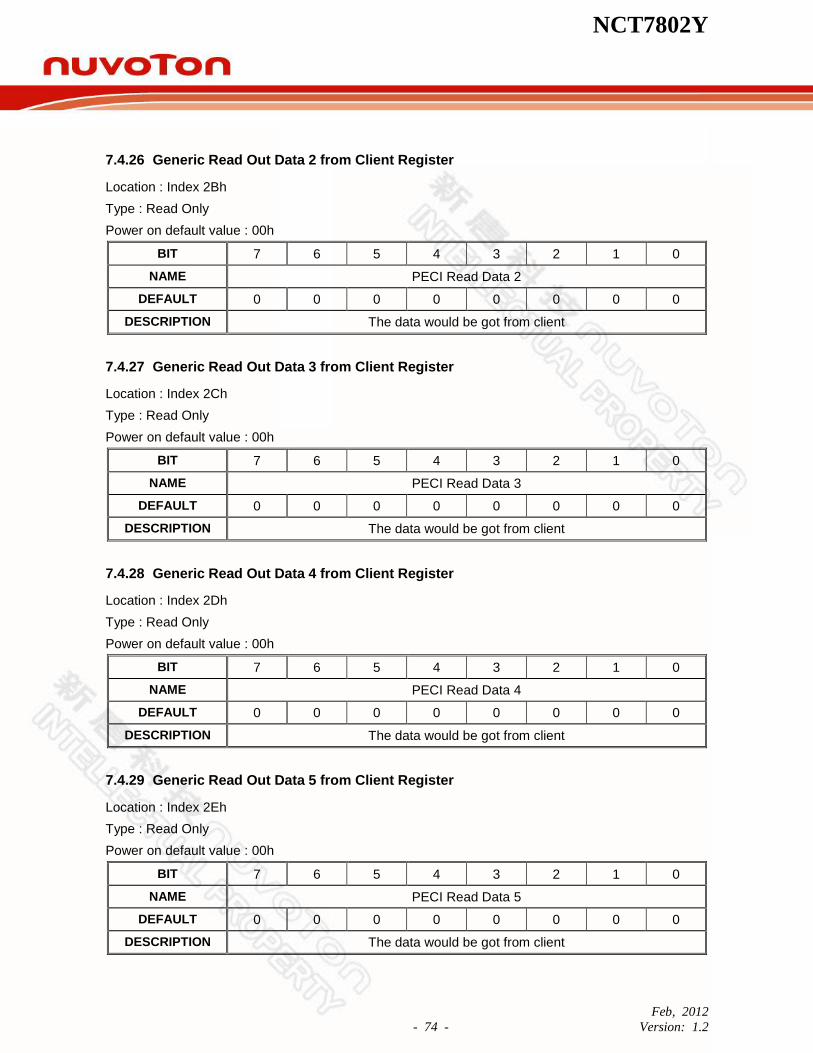
NCT7802Y
Feb, 2012
- 74 - Version: 1.2
7.4.26 Generic Read Out Data 2 from Client Register
Location : Index 2Bh
Type : Read Only
Power on default value : 00h
BIT 7 6 5 4 3 2 1 0
NAME PECI Read Data 2
DEFAULT 0 0 0 0 0 0 0 0
DESCRIPTION The data would be got from client
7.4.27 Generic Read Out Data 3 from Client Register
Location : Index 2Ch
Type : Read Only
Power on default value : 00h
BIT 7 6 5 4 3 2 1 0
NAME PECI Read Data 3
DEFAULT 0 0 0 0 0 0 0 0
DESCRIPTION The data would be got from client
7.4.28 Generic Read Out Data 4 from Client Register
Location : Index 2Dh
Type : Read Only
Power on default value : 00h
BIT 7 6 5 4 3 2 1 0
NAME PECI Read Data 4
DEFAULT 0 0 0 0 0 0 0 0
DESCRIPTION The data would be got from client
7.4.29 Generic Read Out Data 5 from Client Register
Location : Index 2Eh
Type : Read Only
Power on default value : 00h
BIT 7 6 5 4 3 2 1 0
NAME PECI Read Data 5
DEFAULT 0 0 0 0 0 0 0 0
DESCRIPTION The data would be got from client

NCT7802Y
Feb, 2012
- 75 - Version: 1.2
7.4.30 Generic Read Out Data 6 from Client Register
Location : Index 2Fh
Type : Read Only
Power on default value : 00h
BIT 7 6 5 4 3 2 1 0
NAME PECI Read Data 6
DEFAULT 0 0 0 0 0 0 0 0
DESCRIPTION The data would be got from client
7.4.31 Generic Read Out Data 7 from Client Register
Location : Index 30h
Type : Read Only
Power on default value : 00h
BIT 7 6 5 4 3 2 1 0
NAME PECI Read Data 7
DEFAULT 0 0 0 0 0 0 0 0
DESCRIPTION The data would be got from client
7.4.32 Generic Read Out Data 8 from Client Register
Location : Index 31h
Type : Read Only
Power on default value : 00h
BIT 7 6 5 4 3 2 1 0
NAME PECI Read Data 8
DEFAULT 0 0 0 0 0 0 0 0
DESCRIPTION The data would be got from client
7.4.33 Generic Read Out Data 9 from Client Register
Location : Index 32h
Type : Read Only
Power on default value : 00h
BIT 7 6 5 4 3 2 1 0
NAME PECI Read Data 9
DEFAULT 0 0 0 0 0 0 0 0
DESCRIPTION The data would be got from client
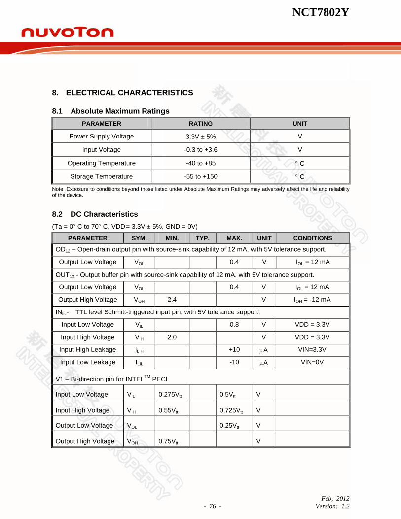
NCT7802Y
Feb, 2012
- 76 - Version: 1.2
8. ELECTRICAL CHARACTERISTICS
8.1 Absolute Maximum Ratings
PARAMETER RATING UNIT
Power Supply Voltage 3.3V 5% V
Input Voltage -0.3 to +3.6 V
Operating Temperature -40 to +85 C
Storage Temperature -55 to +150 C
Note: Exposure to conditions beyond those listed under Absolute Maximum Ratings may adversely affect the life and reliability of the device.
8.2 DC Characteristics
(Ta = 0 C to 70 C, VDD = 3.3V 5%, GND = 0V)
PARAMETER SYM. MIN. TYP. MAX. UNIT CONDITIONS
OD12 – Open-drain output pin with source-sink capability of 12 mA, with 5V tolerance support.
Output Low Voltage VOL 0.4 V IOL = 12 mA
OUT12 - Output buffer pin with source-sink capability of 12 mA, with 5V tolerance support.
Output Low Voltage VOL 0.4 V IOL = 12 mA
Output High Voltage VOH 2.4 V IOH = -12 mA
INts - TTL level Schmitt-triggered input pin, with 5V tolerance support.
Input Low Voltage VIL 0.8 V VDD = 3.3V
Input High Voltage VIH 2.0 V VDD = 3.3V
Input High Leakage ILIH +10 A VIN=3.3V
Input Low Leakage ILIL -10 A VIN=0V
V1 – Bi-direction pin for INTELTM
PECI
Input Low Voltage VIL 0.275Vtt 0.5Vtt V
Input High Voltage VIH 0.55Vtt 0.725Vtt V
Output Low Voltage VOL 0.25Vtt V
Output High Voltage VOH 0.75Vtt V
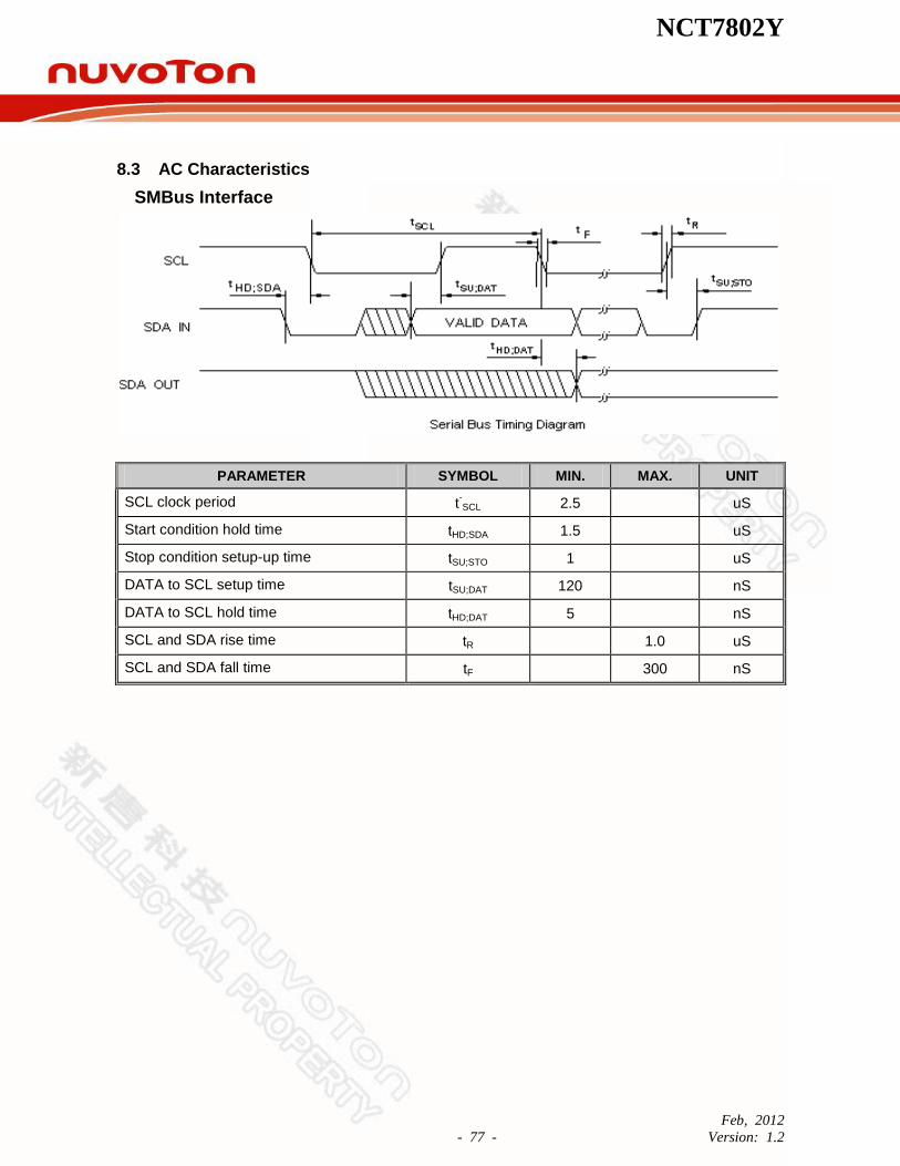
NCT7802Y
Feb, 2012
- 77 - Version: 1.2
8.3 AC Characteristics
SMBus Interface
PARAMETER SYMBOL MIN. MAX. UNIT
SCL clock period t-SCL 2.5 uS
Start condition hold time tHD;SDA 1.5 uS
Stop condition setup-up time tSU;STO 1 uS
DATA to SCL setup time tSU;DAT 120 nS
DATA to SCL hold time tHD;DAT 5 nS
SCL and SDA rise time tR 1.0 uS
SCL and SDA fall time tF 300 nS

NCT7802Y
Feb, 2012
- 78 - Version: 1.2
9. ORDERING INFORMATION
PART NUMBER PACKAGE REMARKS
NCT7802Y QFN20 Green Package (Halogen-free)
10. TOP MARKING SPECIFICATIONS
1st
Line : Nuvoton Logo
2nd
Line : Part number- NCT7802Y
3rd
Line : Assembly tracking code
1 13: packages made in year 2011, week 13
T : Assembly house code
A : IC version
BA : Nuvoton internal use code
NCT7802Y
113TABA

NCT7802Y
Feb, 2012
- 79 - Version: 1.2
11. PACKAGE DRAWING AND DIMENSIONS
QFN20 4x4 MM2
TOP VIEW BOTTOM VIEW
11
620
15
10
15
1616
15 11
10
6
51
20

NCT7802Y
Feb, 2012
- 80 - Version: 1.2
12. REVISION HISTORY
VERSION DATE PAGE DESCRIPTION
1.0 07/13/2011 N.A. Public released, all versions before 1.0 are preliminary versions.
1.1 1/5/2012 2 Added VCC monitoring accuracy item.
1.2 2/2/2012 7,16 Added Programming from EEPROM description.
Important Notice
Nuvoton Products are neither intended nor warranted for usage in systems or equipment, any malfunction or failure of which may cause loss of human life, bodily injury or severe property damage. Such applications are deemed, “Insecure Usage”.
Insecure usage includes, but is not limited to: equipment for surgical implementation, atomic energy control instruments, airplane or spaceship instruments, the control or operation of dynamic, brake or safety systems designed for vehicular use, traffic signal instruments, all types of safety devices, and other applications intended to support or sustain life.
All Insecure Usage shall be made at customer’s risk, and in the event that third parties lay claims to Nuvoton as a result of customer’s Insecure Usage, customer shall indemnify the damages and liabilities thus incurred by Nuvoton.


![Nuvoton Sound Controller Series NSC · 2020. 12. 3. · Nuvoton Sound Controller Series NSC Data Sheet ... VDD_SPK can be floating if PWM+ and PWM- pads unused. [2] Program pad include](https://static.fdocuments.in/doc/165x107/6105f6a527c208602e7e977b/nuvoton-sound-controller-series-nsc-2020-12-3-nuvoton-sound-controller-series.jpg)