
Compact Hard X-Ray Synchrotron Radiation Source with Superconducting Bending Magnets (project)

NORTHWESTERN UNIVERSITY
Synchrotron X-ray Studies of
Epitaxial 2D Material Interfaces
A DISSERTATION
SUBMITTED TO THE GRADUATE SCHOOL
IN PARTIAL FULFILLMENT OF THE REQUIREMENTS
for the degree
DOCTOR OF PHILOSOPHY
Field of Materials Science and Engineering
By
Gavin Paul Campbell
EVANSTON, ILLINOIS
May 2018

2
© Copyright by Gavin Paul Campbell 2018
All Rights Reserved
3
Abstract
Sparked by the isolation of graphene in 2004, the research community has developed a family of
2D materials with distinct functionalities, enabling rapid demonstrations of entirely 2D devices
with applications in energy, electronics, sensors and medicine. The desire to capitalize on the
fantastic properties of 2D materials motivates ongoing efforts to synthesize high-quality 2D
materials on large-scales. Epitaxial deposition of 2D materials on single-crystal substrates yields
large-scale production of 2D materials without compromising crystal quality. However, 2D
material properties are altered depending on the strength of the interactions with the substrate. The
strength of these interactions, from weak van der Waals attractions to strong covalent bonds, are
further revealed by local perturbations to the vertical atomic structure of the interface. For my
dissertation research, I have employed high-resolution synchrotron X-ray characterization
techniques to probe the interface between 2D materials and their growth substrate with atomic
precision on wafer-scales. My dissertation primarily focuses on the interface of elemental 2D
materials and single-crystal substrates, specifically 2D boron (borophene) on Ag(111) and
graphene on Ge(110). The primary objective of these measurements is to resolve outstanding
questions about the strength of interactions and resulting structure of these interfaces. Specifically,
employing X-ray standing wave-enhanced photoelectron spectroscopy, I reveal borophene to be a
highly planar atomic layer of B atoms by constructing a chemically-resolved vertical structure of
borophene with sub-Å precision. Next, I show that epitaxial graphene (EG) atop Ge(110), upon
annealing in ultra-high vacuum (UHV), induces a novel reconstruction of the underlying Ge(110)
surface. I preform a detailed documentation of this structure using a combination of high-
resolution X-ray reflectivity and grazing-incident X-ray diffraction. Finally, I probe the registry of

4
van der Waals epitaxial materials using a combination of grazing-incident X-ray scattering
measurements. Overall, the work presented herein reveals how distinct X-ray surface science
techniques can be employed to resolve outstanding questions about new 2D material interfaces.

5
Acknowledgements
First, I would like to thank my advisor, Prof. Michael Bedzyk, for his fantastic support and
flexibility throughout my time at Northwestern. Mike has an exceptional enthusiasm towards and
mastery of X-ray physics, I am privileged for his mentorship. I want to also thank my committee
members for their time and expertise; Dr. Sang-Soo Lee sharing his X-ray knowledge and Profs.
Lincoln Lauhon and Mark Hersam for their collaboration and leadership within the MRSEC and
valuable insights over the years.
I am grateful to my many collaborators for their contributions and support, without whom
this work would not have been possible. I would like to thank Jade Balla, Xiaolong Lu, Haddalia
Bergeron, Brian Kiraly, and Andrew Mannix for providing samples and challenging me to think
more deeply. Each of them their work is represented in this dissertation. I extend special thanks to
Andrew Mannix for bringing borophene to the United Kingdom. I would also like to thank Robert
Jacobberger and Prof. Michael Arnold for providing samples and my coworkers in the MRSEC
Leadership council for providing feedback.
My colleagues in the Bedzyk group have supported me throughout my time here. Early on,
I benefited from the UHV and X-ray knowledge of Martin McBriarty and Sven Stolz. From the
beginning, Jon Emery provided a foundation for me to build upon and has provided continuous
support throughout my time and Sumit Kewalramani has been an excellent mentor throughout the
years. My contemporaries in the Bedzyk group: Boris Harutyunyan, Xiao Chen, Liane Moreau,
Changrui Gao, and Kurinji Krishnamoorthy have been a constant source of support and friendship,
further enriched by Katherine Harmon, for insights into interface science; Stephanie Moffitt, for
her writing expertise; Bor-Rong Chen, for getting me started in the X-ray lab; and Li Zeng for our

6
meaningful conversations during beamtime. I am also grateful for my interactions with Guennadi
Evmenenko, Achari Kondapalli, Bo-Hong Liu, Jeffery Chen, Elise Goldfine, Anusheela Das,
Curtis Leung, I-Cheng Tung, Janak Thapa, Bruce Buchholz, and Jerry Carsello.
I have also greatly benefited from facilities and staff support at Argonne National Lab and
Diamond National Lab. Several beamline staff members were instrumental in this work, Zhan
Zhang and Christian Schlepütz of Sector 33 and Joe Strzalka of Sector 8. Special thanks go to the
staffs of Sector 5 and I09, specifically Denis Keane of Sector 5 and Tien-Lin Lee of I09, who both
showed extraordinary commitment to the success of the users at their beamlines. Lastly, I thank
Jörg Zegenhagen for his guidance and Paul Fenter and his group for teaching me the fundamentals
of X-ray data analysis.
Of course, I would like to acknowledge my family and friends for their support. I am
grateful to my parents, Scot and Melanie, for nurturing my curiosity and providing an academically
enriching environment. I am thankful to my brothers, Eric and Colin, and my sister, Caitlin, for all
their support and for our adventures through Europe. I am grateful to Alex, Ross, and Bradley for
their enduring friendship. Finally, I would like to thank Kathleen for her phenomenal support and
enduring companionship.
I also acknowledge the financial support I received from the Northwestern Materials Science and
Engineering Center and the National Science Foundation, particularly for supporting my many
trips to Argonne and international trip to Diamond.

7
For Kathleen,
looking forward

8
List of Abbreviations
2D Two Dimensional
AFM Atomic Force Microscopy
BP Black Phosphorus
CCD Charge-Coupled Device
CTR Crystal Truncation Rod
CVD Chemical Vapor Deposition
DFT Density Functional Theory
EAL Effective Attenuation Length
EBE E-Beam Evaporator
EG Epitaxial Graphene
FCC Face-Centered Cubic
FWHM Full-Width Half-Maximum
GISAXS Grazing incidence Small-Angle X-ray Scattering
GIWAXS Grazing incidence Wide-Angle X-ray Scattering
GIXD Grazing incidence X-ray Diffraction
GIXS Grazing Incidence X-ray Scattering
hBN hexagonal Boron Nitride
IMFP Inelastic Mean Free Path
LEED Low-Energy Electron Diffraction
MBE Molecular Beam Evaporator
MMS Metalized Molecular Stripes
NIXSW Normal Incidence X-ray Standing Wave
OPA Octadecylphosphonic Acid
PVD Physical Vapor Deposition
QCM Quartz Crystal Monitor
SAM Self-Assembled Monolayer
SE2DM Synthetic Elemental 2D Material

9
STM Scanning Tunneling Microscopy
STS Scanning Tunneling Spectroscopy
TMD Transition Metal Dichalcogenide
TMFP Transport Mean Free Path
UHV Ultra-High Vacuum
vdW van der Waals
XPS X-ray Photoelectron Spectroscopy
XRF X-ray Fluorescence
XRR X-ray Reflectivity
XSW X-ray Standing Wave
10
Table of Contents
Abstract ........................................................................................................................................... 3
Acknowledgements ......................................................................................................................... 5
List of Abbreviations ...................................................................................................................... 8
Table of Contents .......................................................................................................................... 10
List of Figures ............................................................................................................................... 12
List of Tables ................................................................................................................................ 14
Chapter 1: Overview ..................................................................................................................... 15
1.1: Motivation: Material Interfaces in 2D................................................................................ 15
1.1: Outline ................................................................................................................................ 16
Chapter 2: Fundamentals of two dimensional materials ............................................................... 20
2.1: Materials Stable in Two Dimensions ................................................................................. 20
2.2: 2D material synthesis ......................................................................................................... 22
2.3: Properties of Graphene ....................................................................................................... 24
2.4: Properties Elemental 2D Materials .................................................................................... 26
Chapter 3: Structure of 2D Materials on Substrates ..................................................................... 29
3.1: Interactions at interfaces .................................................................................................... 29
3.2: Epitaxial Graphene on Single-Crystals .............................................................................. 30
3.3: Epitaxial Borophene ........................................................................................................... 37
3.4: vdW Epitaxy....................................................................................................................... 40
Chapter 4: X-ray Characterization Techniques............................................................................. 41
4.1: Introduction to X-ray physics............................................................................................. 41
4.2: X-ray standing wave .......................................................................................................... 51
4.3: Crystal Truncation Rod ...................................................................................................... 57
4.4: Grazing incidence X-ray diffraction .................................................................................. 60
4.5: X-ray Photoelectron Spectroscopy ..................................................................................... 63
4.6: Other Spectroscopy ............................................................................................................ 67
Chapter 5: B/Ag(111) Interface .................................................................................................... 69
5.1: Abstract .............................................................................................................................. 69

11
5.2: Introduction ........................................................................................................................ 69
5.3: Methods .............................................................................................................................. 72
5.4: Synthesis ............................................................................................................................ 76
5.5: Results ................................................................................................................................ 82
5.6: Conclusions ........................................................................................................................ 96
Chapter 6: EG/Ge(110) Reconstruction ........................................................................................ 97
6.1: Introduction ........................................................................................................................ 97
6.2: Methods .............................................................................................................................. 99
6.3: Results .............................................................................................................................. 102
6.4: Conclusions ...................................................................................................................... 111
Chapter 7: EG/SiC(0001) Heterostructures ................................................................................ 112
7.1: Introduction ...................................................................................................................... 112
7.2: Methods ............................................................................................................................ 113
7.4: Results .............................................................................................................................. 116
7.5: Conclusions ...................................................................................................................... 130
Chapter 8: Future Work .............................................................................................................. 131
8.1: Borophene on Au(111) ..................................................................................................... 131
8.2: Blue Phosphorus............................................................................................................... 131
References: .................................................................................................................................. 133
Appendix A: Ag(111) XPS-XSW ............................................................................................... 147
A.1: Type equation here.Oddities in Photoelectron Yields ................................................... 147
Appendix B: Data sets ................................................................................................................ 151
B.1: GIXD Data for “6×2” EG/Ge(110) ................................................................................. 151
12
List of Figures
Figure 2.1: The crystal structure of graphene, defined by lattice vectors aEG and bEG. ................ 24
Figure 2.2: Schematic of graphene ............................................................................................... 25
Figure 2.3: Predicted 2D phosphorus crystal structures ............................................................... 27
Figure 3.1: C 1s photoelectron spectra of graphene ..................................................................... 34
Figure 3.2: The vertical electron density profile of EG on SiC(0001) ......................................... 36
Figure 3.3: Borophene lattice and atomic structures .................................................................... 38
Figure 3.4: Proposed atomic models for borophene on Ag(111) .................................................. 40
Figure 4.1: Simulated X-ray standing wave measurement of borophene ..................................... 56
Figure 4.2: Schematic of crystal truncation rod ............................................................................ 59
Figure 4.3: GIXS geometric setup ................................................................................................ 63
Figure 5.1: Borophene synthesis and atomic structures ............................................................... 71
Figure 5.2: Diagram of the I09 beamline at Diamond. Experimental was performed in the EH2
end-station using hard and soft X-rays from separate undulators. (From Ref. [169]) .................. 72
Figure 5.2: Fermi edge measurements .......................................................................................... 75
Figure 5.3: Reciprocal space analysis of in-plane borophene atomic structure ............................ 78
Figure 5.4: LEED patterns of 300 °C Borophene ......................................................................... 81
Figure 5.5: High-resolution XPS of borophene ............................................................................ 82
Figure 5.6: XPS survey, C 1s, and O 1s spectra of borophene ..................................................... 84
Figure 5.7: XPS of 20 °C deposited multilayer boron .................................................................. 85
Figure 5.8: Angular-resolved boron 1s XPS ................................................................................. 86
Figure 5.9: XSW characterization of silver .................................................................................. 88
Figure 5.10: XSW characterization of 20 °C deposited multilayer boron .................................... 89
Figure 5.11: XSW characterization of the borophene .................................................................. 90
Figure 5.12: XSW characterization of the in-plane borophene .................................................... 92
Figure 5.13: In-plane atomic model structure ............................................................................... 94
Figure 6.1: STM images of graphene on Ge(110) ........................................................................ 98
Figure 6.2: STM data of annealed EG/Ge(110) .......................................................................... 102
Figure 6.3: Spectra of as-grown and annealed EG/Ge(110) samples ......................................... 103

13
Figure 6.4: XRR data of EG/Ge(111) ......................................................................................... 105
Figure 6.5: Lattice of annealed EG/Ge(110) ............................................................................... 107
Figure 6.6: GIXD surface characterization of EG/Ge(110) ........................................................ 109
Figure 7.1: CVD-grown MoS2 on EG......................................................................................... 117
Figure 7.2: Rotationally commensurate van der Waals epitaxy of MoS2 on EG ....................... 119
Figure 7.3: Examination of the growth orientation of MoS2 ...................................................... 120
Figure 7.4: XRR data .................................................................................................................. 122
Figure 7.5: GIWAXS measurements .......................................................................................... 125
Figure 7.6: AFM of degraded MoS2 flakes on EG/SiC .............................................................. 127
Figure 7.7: AFM of MMS ........................................................................................................... 127
Figure 7.8: Grazing incidence small and wide-angle X-ray scattering ....................................... 130
Figure A.1: Flowchart describing the procedure to collect and analyze data at I09. .................. 147
Figure A.2: X-ray standing wave (XSW) characterization of silver .......................................... 149
Figure A.3: X-ray photoelectron spectroscopy fitting parameters of Ag 3d spectra during X-ray
standing wave characterization ................................................................................................... 150

14
List of Tables
Table 3.1: The closest separation in EG/M ................................................................................... 31
Table 5.1: Energies and angles to access Ag Bragg conditions. ................................................... 74
Table 5.2: QCM measured B deposition rate ................................................................................ 79
Table 5.3: XPS fitting parameters for Soft and Hard B 1s X-ray spectra ..................................... 83
Table 5.4: XPS fitting parameters for Soft and Hard Ag 3d X-ray spectra .................................. 85
Table 5.5: For the two deposition temperatures, XPS determined boron percent ........................ 87
Table 5.6: Coherent fraction (fH) and coherent Position (PH) of B ............................................... 93
Table 6.1: Results of model dependent fit to XRR data ............................................................. 104
Table A.1: Coherent fractions (f300°C), maximum normalized yields (Ymax), and corresponding
maximum intensity (Imax) of Ag 3d5/2 photoelectron yields ........................................................ 148
Table B.1: Measured 𝐹ℎs𝑘s2 for Ge(110) “6×2” reconstruction. .............................................. 151
15
Chapter 1: Overview
1.1: Motivation: Material Interfaces in 2D
The successful isolation and characterization of graphene in 2004, revealed new materials
physics (e.g. relativistic charge carriers [1]) and launched the now densely populated field of two-
dimensional (2D) materials. The arena of 2D materials now includes elemental and compound
planar and buckled structures, with an equally diverse set of electronic, mechanical, and optical
properties. The onset of these new materials properties follows the vertical confinement of
electrons, owing to the isolation of individual atomic layers, which are typically derived from
weakly van der Waals (vdW) bonded sheets of a hexagonal bulk crystal (e.g. graphene from
graphite). With range of exceptional electronic properties now accessible at the 2D limit, the desire
to utilize these materials in large scale device applications has motivated the development of
scalable growth methods of single-crystal high-quality 2D materials on technologically relevant
substrates. Though the in-plane structure of these materials is robust, 2D materials nonetheless
interact with their local environment, thereby imparting 2D materials with functions beyond their
intrinsic properties [2,3]. Interestingly these interactions are, in some cases, strong enough to
stabilized novel 2D structures, offering a means to dramatically expand the scope of 2D materials
beyond those derived from bulk crystals [4]. This has driven the development of so-called synthetic
2D materials [e.g. 2D boron (borophene) [5,6] and 2D silicon (silicene) [7]] which lack direct bulk
analogs.
The formation of these new 2D structures at single-crystal interfaces present a myriad of
characterization challenges, owing to degeneracy in plausible planar-like surface structures. This
problem is ubiquitous in the field of 2D materials owing to ambiguity in distinguishing free-

16
standing 2D materials from surface alloys [8,9], subsurface precipitates [10], or interfacial
reconstructions, particularly when investigating systems where the atomic structure of the surface
and interface are both unknown. Distinguishing a 2D material from other surface features is of
paramount importance when interpreting materials characteristics, as the salient properties of the
system can depend heavily on their position relative to the supporting substrate. Even for a vdW
bonded 2D material, the interface structure influences strain, doping, and symmetry of the 2D
overlayer [11-13]. Thus, understanding the interface between a 2D material and single-crystal
substrate necessities the use of chemically sensitive structural characterization with sub-Å
resolution [14]. This challenge bodes well for study through X-ray interface science, in particular
by using X-ray spectroscopy to impart chemical specificity to Ångström-resolution X-ray
diffraction measurements. This dissertation demonstrates the use of synchrotron-based X-ray
tools, primarily X-ray standing wave (XSW), crystal truncation rod (CTR), and grazing incidence
X-ray diffraction (GIXD), to solve the physics and chemistry of new surface structures, with an
emphasis on determining the interface structure of 2D structures on a given substrate.
1.1: Outline
In this document, I explore the structure of interfaces between epitaxial 2D materials and
their substrate. My work primarily focuses on elemental 2D materials, therefore in chapter 2, I
describe the origin of the characteristic properties of these materials and how a common set of
bonding configurations which lead to a diverse array of elemental 2D structures. I focus on
graphene and black phosphorus as prototypical elemental 2D materials with a planar and buckled
bonding configuration, respective. I discuss how these structures inform our understanding of new
2D materials which lack corresponding bulk allotropes.

17
The discussion of 2D materials is further expanding upon in chapter 3 by introducing
interactions of epitaxial 2D materials with their growth substrate. I review graphene on metal
substrates to demonstrate how the C-Metal interaction strength generates perturbations in the
vertical structure of the overlaying graphene accompanied by changes to the electronic properties
of graphene. I describe how rigidly bound covalent substrates, such as graphene on Ge and
graphene on SiC, circumvent these interactions to yield pristine monolayer graphene. Finally, I
introduce van der Waals epitaxy which has the potential to yield high-quality graphene with
minimal substrate interactions.
In chapter 4, I establish the principles of X-ray interface science techniques which I used
in my dissertation research to deduce the vertical structure of 2D materials and their interface.
Initially, I introduce the kinematic and dynamic theory of X-rays interaction with matter, which I
then expand upon to the theory of X-ray standing wave-enhanced photoelectron spectroscopy
(XSW-XPS), crystal truncation rod (CTR), and grazing-incidence X-ray diffraction (GIXD).
Chapter 5 describes my collaborative efforts with Andrew Mannix to resolve the interface
structure of two distinct phases of borophene on Ag(111). Using XSW-XPS, we resolve the
positions of boron in multiple chemical states with sub-Ångström spatial resolution, revealing that
the borophene forms a single planar layer that is 2.4 Å above the unreconstructed Ag surface.
Moreover, our results reveal that multiple borophene phases exhibit these characteristics, denoting
a unique form of polymorphism consistent with recent predictions.
In chapter 6, I probe the interface between epitaxial graphene and Ge(110) employing
scanning tunneling microscopy (STM), GIXD, and high-resolution X-ray reflectivity (XRR)
experiments. We present a thorough study of epitaxial graphene (EG)/Ge(110) and report a
18
Ge(110) “6×2” reconstruction stabilized by the presence of epitaxial graphene unseen in group-IV
semiconductor surfaces. Our X-ray studies reveal that graphene resides atop the surface
reconstruction with a 0.34 nm van der Waals (vdW) gap and provides protection from ambient
degradation.
In chapter 7, I explore the interface and in-plane structure of multi-dimensional vdW
epitaxy on EG on SiC(0001). First, we examine here the thickness-controlled vdW epitaxial
growth of MoS2 on EG via chemical vapor deposition, which gives rise to transfer-free synthesis
of a 2D heterostructure with registry between its constituent materials. The rotational
commensurability observed between the MoS2 and EG is driven by the energetically favorable
alignment of their respective lattices and results in nearly strain-free MoS2, as evidenced by
synchrotron X-ray scattering. We proceed to investigate the structure of metal deposited on
octadecylphosphonic acid (OPA), which forms a 1D heterostructure in registry with the underlying
graphene. We examine the orientational registry and long-range structure of the OPA molecules
using GIXD techniques and confirm the molecules are well align and could act as a catalytic
template for further chemistry.
Finally, in chapter 8, I review 2D materials systems reported in the literature that bode well
for study using X-ray interface techniques. I discuss theoretical results of borophene polymorphs
grown on Au(111), which are predicated to have a distinct vertical and in-plane structure from
borophene atop Ag(111) owing to weaker interactions with the substrate. I also discuss a recent
report of 2D blue phosphorus stabilized by Au(111), which appears to deviate in structure from
theoretical predications and bulk measurements.

19
Appendices are included to supplement discussion in the main chapters. Appendix A
describes unresolved sources of error seen in the XPS analyser at I09. Appendix B includes a
complete dataset for the GIXD analysis performed in chapter 6.
20
Chapter 2: Fundamentals of two dimensional
materials
2D materials are discrete planar layers defined by strong in-plane bonding that imparts
stability to atomically thin layers, and weak out-of-plane interactions which make them distinct
from their supporting substrate [15]. Crystallographically, a 2D material can be defined using two
lattice parameters, which should be non-degenerate when compared to a bulk lattice. The exact in-
plane bonding structure of the 2D material often leads to emergent properties distinct from bulk
counterparts.
2.1: Materials Stable in Two Dimensions
2.1.1: Thermodynamically unstable materials
2D materials, theoretically formed from reducing bulk crystals to single atomic planes, have
introduced a new engineering approach to materials. Despite early demonstrations of covalently
bonded atomic layers on metals [16-18] or SiC [19], the notion of free-standing 2D materials were
suggested to be unstable owing to thermal fluctuations which would ultimately destabilize the
material [20]. At the time, it was believed that the thermal fluctuations in atomically thin crystals
were greater than interatomic interaction strength, thereby requiring a 3D bulk crystal to stabilize
2D structures. These assertions were challenged by the successful isolation of graphene (a single
atomic layer of graphite) in 2004 [21], and even more so with the demonstration of suspended
membranes [15]. The strong in-plane C-C covalent bonds were critical for stabilizing graphene
and other 2D materials, making them robust to thermal fluctuations.
21
2.1.2: Bonding in 2D materials
2D materials are discrete atomic layers, distinct from other surface structures (i.e. surface
reconstructions and compounds), owing to both strong intramolecular bonding and weak
interactions with their surroundings which enables the formation of discrete structures of purely
surface. These purely surface structures exhibit properties distinct from the bulk surface, owing to
unbound orbital interactions across the 2D material and the confinement of the electronic structure
down to a single atomic layer. Even at the few-layer limit, these unbound orbitals interact across
the layers, adding new electronic states to the system. In fewer than ten atomic layers, 2D materials
achieve bulk-like properties, so the successful isolation of the material at the single layer limit is
crucial.
In-plane covalent bonding not only stabilizes 2D materials, it also dictates the exact structure
of the material and it need not be entirely planar. Planar structures such as graphene and hexagonal
boron nitride (hBN), are mechanically robust covalent planar hexagonal networks formed from a
single layer of sp2-hybridized atoms. Whereas mixed sp3- and sp2-hybridization leads to the
formation of partially buckled structures nonetheless isolated from their surroundings. Compound
structures, such as the covalently bonded of Transition metal dichalcogenides (TMDs), have
unbound sp3 orbitals oriented normal to the surface by the pyramid network of covalent bonds.
Thus, the challenge in the ongoing effort to develop new 2D materials is two-fold: synthesize
structures stabilized by strong intraplanar bonding and isolate these structure from their
surroundings.
22
2.2: 2D material synthesis
Initially, isolation of 2D materials was achieved through mechanical exfoliation (i.e. the
scotch tape method) of bulk material, yielding micron-sized sheets of single atomic layers.
Novoselov and Geim’s scotch-tape method [21] has been widely adopted by the research
community for its simplicity to produce well-isolated pristine samples. This approach exclusively
produces flakes of 2D material from bulk 3D allotropes and cannot be used to generate new 2D
structure or reliably synthesize large-area sheets of 2D materials. Epitaxial growth [e.g. chemical
vapor deposition (CVD) and physical vapor deposition (PVD)] [22] on single-crystal substrates
has proven the most reliable approach towards producing pure large-area 2D materials [23]. In
contrast to traditional monolayers, which rely critically on lattice matching between adatoms and
the surface, the interfacial interactions of 2D materials are superseded by the formation of the
strong in-plane covalent bonding characteristic of 2D materials. Thus, even when the substrate
interactions relatively strong, it is possible to produce an atomic layer of a single-crystal 2D
structure across large-areas with an unperturbed in-plane structure.
2.2.1: Chemical Vapor Deposition
Chemical vapor deposition (CVD) employs high-purity molecular precursors (e.g. methane)
on a catalytically active substrate to which combine to form solid layers on the surface [24]. The
precursors, though most commonly gaseous, also include liquids and solids vapor, flown in an
inert gas to the substrate target. Heating of the substrate during or after deposition is often
necessary to both decompose the precursors and allow diffusion of species on the surface to form
uniform films. Synthesis conditions vary, reflected by a myriad of classifications used to reflect
the parameters of the CVD process.

23
2.2.2: Physical Vapor Deposition
Physical vapor deposition (PVD) typically involves deposition of atomic species via
molecular beam evaporator (MBE) using an e-beam evaporator (EBE), Knudsen cell, or other solid
phase deposition source under ultra-high vacuum (UHV). The atomic sources used are typically
high-purity with well calibrated deposition rates, enabling growth of desired fractions of 2D
monolayers achieved by adjusting the deposition time. Introduction of reactive gaseous molecules
in series with atomic deposition expands the capabilities of PVD. Layer-by-layer growth of binary
alloys is possible, but typically requires specialized systems equipped with sub monolayer in situ
monitoring analysis, meant to grow a specific class of materials. Apart from in situ growth rate
monitoring, UHV enables measurements of the pristine material using techniques only suitable in
vacuum.
2.2.3: Growth from bulk Material
Selective etching and isolation in solution-based systems is among the most common
approaches to isolate 2D materials from bulk [25,26]. Though the strengths of this approach are
the production large quantity of multilayer, rather than the growth of high-quality films. Isolation
of 2D materials from the bulk can also be achieved through the selective diffusion of a specific
bulk species, such as Si from SiC. Once the C-rich SiC(0001) 6√3 × 6√3 buffer layer achieves a
sufficiently high C concentrations, the excess C condenses into a graphitic layer, separated from
Si-dangling bonds. This separation can occur also by passivation the surface with gaseous species,
which has also been shown to stabilize films grown by other methods [27].
24
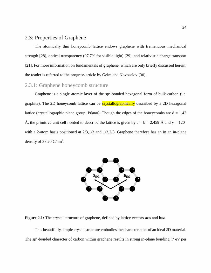
2.3: Properties of Graphene
The atomically thin honeycomb lattice endows graphene with tremendous mechanical
strength [28], optical transparency (97.7% for visible light) [29], and relativistic charge transport
[21]. For more information on fundamentals of graphene, which are only briefly discussed herein,
the reader is referred to the progress article by Geim and Novoselov [30].
2.3.1: Graphene honeycomb structure
Graphene is a single atomic layer of the sp2-bonded hexagonal form of bulk carbon (i.e.
graphite). The 2D honeycomb lattice can be crystallographically described by a 2D hexagonal
lattice (crystallographic plane group: P6mm). Though the edges of the honeycombs are d = 1.42
Å, the primitive unit cell needed to describe the lattice is given by a = b = 2.459 Å and ɣ = 120°
with a 2-atom basis positioned at 2/3,1/3 and 1/3,2/3. Graphene therefore has an in an in-plane
density of 38.20 C/nm2.
Figure 2.1: The crystal structure of graphene, defined by lattice vectors aEG and bEG.
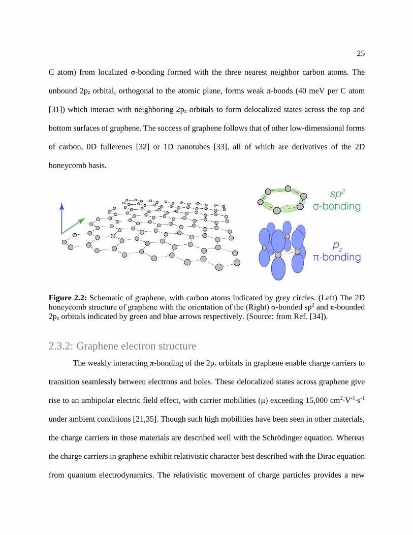
This beautifully simple crystal structure embodies the characteristics of an ideal 2D material.
The sp2-bonded character of carbon within graphene results in strong in-plane bonding (7 eV per
25
C atom) from localized σ-bonding formed with the three nearest neighbor carbon atoms. The
unbound 2pz orbital, orthogonal to the atomic plane, forms weak π-bonds (40 meV per C atom
[31]) which interact with neighboring 2pz orbitals to form delocalized states across the top and
bottom surfaces of graphene. The success of graphene follows that of other low-dimensional forms
of carbon, 0D fullerenes [32] or 1D nanotubes [33], all of which are derivatives of the 2D
honeycomb basis.
Figure 2.2: Schematic of graphene, with carbon atoms indicated by grey circles. (Left) The 2D
honeycomb structure of graphene with the orientation of the (Right) σ-bonded sp2 and π-bounded
2pz orbitals indicated by green and blue arrows respectively. (Source: from Ref. [34]).
2.3.2: Graphene electron structure
The weakly interacting π-bonding of the 2pz orbitals in graphene enable charge carriers to
transition seamlessly between electrons and holes. These delocalized states across graphene give
rise to an ambipolar electric field effect, with carrier mobilities (μ) exceeding 15,000 cm2∙V-1∙s-1
under ambient conditions [21,35]. Though such high mobilities have been seen in other materials,
the charge carriers in those materials are described well with the Schrödinger equation. Whereas
the charge carriers in graphene exhibit relativistic character best described with the Dirac equation
from quantum electrodynamics. The relativistic movement of charge particles provides a new
26
means to explore predictions of (2+1)-dimensional quantum electrodynamics [36-38]. The
interaction between these charge carriers and the graphene lattice gives rise to Dirac fermions,
where electrons with no effective mass (me) give rise to a linear dispersion relation and ballistic
transport of charge carriers near with drift velocities (vd) = 106 m∙s-1.
2.4: Properties of Elemental 2D Materials
The collection of elemental 2D materials capable of forming strongly covalently bonded
networks are referred to as Xenes. Of the Xenes, only two elements, C and P, have known layered
bulk allotropes [i.e. graphite and black phosphorus (BP)]. The remaining Xenes (Si, B, Ge, and
Sn) are so-called synthetic elemental 2D materials (SE2DMs), and have no corresponding bulk
allotropes. SE2DMs are synthesized through appropriate choice of substrate, which suppresses the
energy cost of planar configurations of atoms below otherwise thermodynamically favorable bulk
nanoclusters. Although several stable SE2DM structures have been proposed by theory [39,40],
experimental verification of these proposed structures, particularly when isolated from their
supporting substrate, are relatively sparse owing to rapid degradation under ambient conditions
[6]. Thus, it remains unclear if SE2DMs would remain intact as freestanding 2D layers when
isolated from their support substrate.
2.4.1: Buckled 2D structures
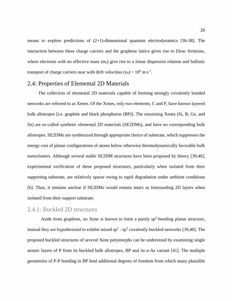
Aside from graphene, no Xene is known to form a purely sp2-bonding planar structure,
instead they are hypothesized to exhibit mixed sp2 - sp3 covalently buckled networks [39,40]. The
proposed buckled structures of several Xene polymorphs can be understood by examining single
atomic layers of P from its buckled bulk allotropes, BP and its α-As variant [41]. The multiple
geometries of P-P bonding in BP lend additional degrees of freedom from which many plausible
27
buckled 2D allotropes have been derived. Four 2D phosphorus (α-P, β-P, ɣ-P, and δ-P) allotropes
[42] have been computationally predicted by geometrical manipulations of P-P bonding in
monolayer BP with blue phosphorus (β-P; a single atomic layer of α-As BP [43]) recently
synthesized experimentally [44]. Nine others predicted P allotropes have been predicted through
more aggressive alterations [45] of BP.
Figure 2.3: Predicted 2D phosphorus crystal structures of (a) α-P (BP; black phosphorus), (b) β-
P (blue phosphorus), (c) ɣ-P, and (d) δ-P with the unit cell shown by a grey box outlined with a
black dotted line and basis vectors a1 and a2 shown in red. The modifications to the lattice to
construct these phases is shown for (e) β-P from α-P, (f) β-P from ɣ-P, and (g) ɣ-P from δ-P
(Source: adapted from Ref. [42])
While 2D phosphorus and 2D carbon have layered bulk allotropes, which provide a basis
for structure determination, the structure of SE2DMs requires more advanced surface
characterization techniques, the interpretation of which are further hampered by substrate
influence. Like BP, multiple 2D buckled allotropes of silicene (3x3[7], √13x√13, √7x√7, and
√3 × √3 [8,46]) have been proposed. The challenges in determining the structure of SE2DMs are
α-P
β-P
ɣ-P β-P
δ-P
ɣ-P
(e) (f) (g)
28
evident from ongoing efforts to characterize the √3 × √3 phase of silicene on Ag(111). Initially,
this phase was attributed to a free-standing buckled honeycomb silicene structure [40], similar to
β-P. A √3 × √3 phase of Si deposited on Ag(111) observed by scanning tunneling microscopy
(STM) [46] was attributed to the formation of a honeycomb silicene structure, which was further
validated by first-principles calculations [47]. Further structural analysis of the √3 × √3 phase of
silicene revealed it to share striking similarities to an Ag-Si reconstruction atop bulk Si layers [8],
which match rigorous structural analysis of an Ag-induced (√3 × √3)R30° reconstruction of
Si(111) [48]. Likewise, recent theoretical work of Si on Ag(111) reveals the formation of Si-Ag
alloys to be energetically favorable to freestanding Si [10].
2D Boron (borophene), like silicene, shows multiple structures when synthesized on
Ag(111). Like other SE2DMs, STM analysis of borophene matches simulated STM images from
theoretically predicted buckled structures [6]. The same structure seen in STM also match a
vacancy mediated [49] structure. These phases are discussed in greater detail in chapter 3, and in
chapter 5 we report the results of our investigation into the interface structure of borophene on
Ag(111).

29
Chapter 3: Structure of 2D Materials on
Substrates
3.1: Interactions at interfaces
2D materials, being atomically flat structures, bode well to epitaxial growth on single-
crystal substrates. The interfaces between 2D materials and substrates differ from other monolayer
materials owing to the formation of strong in-plane covalent bonds, which supersede substrate
interactions by an order of magnitude that would otherwise lead to adlayer formation. Nonetheless,
the interaction strength between growth substrates and 2D materials often exceed the forces in bulk
vdW solids, ranging from physisorption [50] to strong hybridization of atomic sites in the 2D
material [51]. By breaking the quantum confinement with a reactive substrate, 2D materials can
develop strain, doping, and structural changes in response [11-13]. Controlling the degree of
interaction at this interface is therefore critical to retain the desired properties of 2D materials.
Substrate choice is often restricted to materials with sufficient catalytic interactions, which
are vital for bottom-up synthesis of 2D materials via CVD and PVD. The precise interaction
strength of the synthesized 2D material and the substrate is revealed by the vertical distances
between them, revealing the types of bonding present in the system. Covalently bonded substrates
and surface compounds, show a maximum vertical separation equal to the covalent bond length
(e.g. 1.54 Å for diamond), which is further reduced when the covalent bond is off-normal with
respect to the substrate surface. While weakly interacting substrates via vdW epitaxy [52] show a
gap similar to a vdW bonded bulk solid (e.g. 3.36 Å for graphene). Therefore, directly measuring
the interface structure elucidates the bonding present at the interface. For 2D materials with bulk

30
allotropes, epitaxy is primarily a means to produce high-quality 2D crystals, and any interactions
with the substrate are inferred from changes to the electronic structure in the 2D material. Whereas
for SE2DMs, substrate interactions are a critical component of stabilizing otherwise
thermodynamically unfavorable structure [53]. Deconvoluting substrate interactions from the
measured properties of SE2DMs is exceptionally challenging without pristine SE2DM properties
as a basis for comparison. Thus, the degree of interaction between substrate and SE2DMs cannot
be easily inferred and instead must be measured directly.
3.2: Epitaxial Graphene on Single-Crystals
Local fluctuations in amorphous and polycrystalline substrates, on the length scale of the
hexagonal honeycomb structure of graphene, introduce periodic impurities in the graphene [54].
The desire to produce grain-boundary free 2D crystals motivated the growth of graphene on single-
crystal surfaces with well-defined terraces [55]. Even when the graphene in-plane structure is
unperturbed, interface scattering of the π-π coupled 2pz orbitals from the substrate can hinder
charge transport [13], which is reflected in the precise interface structure of the epitaxial graphene.
Initial demonstrations of CVD graphene yielded polycrystalline graphene films. The
weakest substrate interactions are unable to impose rotational registry, leading to polycrystalline
graphene, which shows reduced conductivity owing to scattering at the in-plane grain boundaries
[56]. On the other hand, strongly interacting substrates, like Ni, can lead to chemical bonding and
reduced electronic performance [57,58]. Herein, we review the precise interface structure
dependence of epitaxial graphene on metal, Ge, and SiC single-crystals. For a summary of the
growth and characterization of epitaxial graphene, the reader is directed to review articles by
31
Tetlow and Kantorovich [59] and Batzill [60] for graphene on metals, Riedl and Starke [61] and
more recently Norimatsu and Kusunoki [62] for graphene on SiC.
3.2.1: Epitaxial Graphene on Metals
Single-crystal metal substrates were among the first to produce large-area epitaxial
graphene, largely owing to their ability to catalyze carbon CVD precursors. The metal-carbon
interactions which enable graphene epitaxy, leave the in-plane structure of graphene preserved,
owing to extremely ridged in-plane C-C bonding. Biaxial strain is also energetically unfavorable,
as graphene cannot realistically achieve commensuration with a substrate using in-plane strain
more than ~1%, leading to other relaxation mechanisms. Most commonly, the interface structure
between graphene and lattice-mismatched hexagonal array of metal substrate surface atoms is a
vertically corrugated moiré superstructure, where (m × m) graphene unit cells are matched to (n ×
n) substrate unit cells, often rotated either 0° or 30° relative to each other from the hexagonal
symmetry of graphene. The large 2D lattice, formed by the shared lattice points of the epitaxial
graphene (EG) and underlying metal substrate surface atoms, is referred to as the EG/M
superlattice. The distance between carbon and substrate atoms vary considerably across the EG/M
lattice vectors, so too does the interaction strength between the atoms, as is evident from changes
to the C1s photoelectron spectra [63].
Table 3.1: The closest separation in EG/M, measured between parallel planes defined by the
innermost carbon atoms in EG and metal substrate atoms directly underneath them. (Source:
adapted from Ref. [60])
Substrate Closest Separation (Å)
Ni(111) 2.1 [57,58]
Co(0001) 2.1 [64]
Ru(0001) 2.1 [65,66]
Rh(111) 2.2 [67]
32
Re(0001) 2.1 [68]
Pd(111) 2.5 [69]
Cu(111) 3.3 [70]
Pt(111) 3.3 [69-73]
Ag(111) 3.3 [70,72,73]
Au(111) 3.3 [70,72,73]
Ir(111) 3.4 [72,74]
Fe(110) 2.1 [75]
The structure of epitaxial graphene on metals can ranges from covalent-like to vdW-like
with the corresponding gap between 2.1 Å and 3.4 Å, listed in Table 3.1. The interaction between
EG and the substrate show a correlation with d-orbital to π-bond interaction [76]. For the weakly
interacting EG/M with a vdW-like vertical separation, the electronic structure reflects pristine
graphene aside from a shift in the graphene Dirac point owing to charging from the work function
difference between metal and graphene. Whereas strongly interacting substrates induce sp3
bonding character in the overlaying graphene, revealed by a binding energy shift in the carbon 1s
photoelectron spectra and a vertical buckling of the graphene, showing in Figure 3.1.
EG on face-centered cubic (FCC) Ni(111) [57,58] and EG on Hexagonal Co(0001) [64]
show among the strongest EG/M interactions and best lattice matching (lattice mismatch < 2%),
with band hybridization occurring between the metal d-electrons and the graphene π-orbitals. The
(111) surface of Ni and (0001) surface of Co are in (1×1) registry with graphene, and therefore
does not form a moiré superstructure. The EG interacts strongly with the underlying substrate,
buckling slightly and sitting 2.11 Å and 2.16 Å atop the Ni(111) surface [57]. Similar values are
achieved for EG atop Co(0001) [64]. The graphene-Ni interactions are strong enough to form
carbide compounds at low temperatures [77,78]. Nonetheless, the absorption energy of graphene

33
on Ni(111) is comparable to physisorption (70 meV per C atom) [79], making it a useful substrate
for subsequent transfer.
EG on Ru(0001) [65] [66], Rh(111) [67], and Re(0001) [68] also show strong EG/S
interactions, showing a minimum surface separation of 2.1 Å. These metals are highly lattice
mismatched with graphene, a corrugated moiré structure forms to accommodate the mismatch.
The (23x23) Ru(0001), (11x11) Rh(111), and (9x9) Re(0001) moiré patterns showing areas
buckled outward 0.6 – 1.6 Å , 1.5 Å, and 1.6 Å, respectively.
Graphene shows weaker interfacial interactions with the noble metals, Cu(111), Pt(111),
Ag(111), Au(111) and Ir(111) [70,72,73]. These interactions are not fully vdW, as is evident by
the formation of moiré patterns to accommodate the lattice mismatch between EG and these
metals. The EG/Ir(111) moiré pattern shows a 3.41 Å vertical gap, but with undulations of no
more than 1.0 Å [74]. This ~1.0 Å has been attributed to graphene physisorption and chemisorption
across the Ir(111) surface. These weakly interacting systems also allow the formation of multiple
orientations of EG, even when in epitaxial registry, as was the case for graphene on Cu(111) [80].
EG on Fe(110) [75] is distinct from other metals as there is no symmetry matching between
substrate and EG, which is typically needed for epitaxy. The graphene is strongly electronically
coupled to the underlying Fe(110) substrate and stabilized by the formation of long-range
corrugations with a ~4 nm period. The stability of these corrugations is compromised at elevated
temperatures (630 °C), resulting in carbide formation.
34
Figure 3.1: C 1s photoelectron spectra of graphene taken using a 400 eV X-ray source. Spectra
are from monolayer graphene on metal substrates, with highly ordered pyrolytic graphite given as
a reference standard. (Source: from Ref. [63])
3.2.2: Epitaxial Graphene on Ge
Epitaxially aligned graphene on the (110) face of single-crystal Ge offer a means to produce
high-quality graphene without the fermi-energy shifting associated with metal substrates [81]. The
zig-zag and armchair directions of graphene lie parallel to the [001] and [1̅10] directions of the
Ge(110) face, making a perfect large-area single-crystal with superior electronic properties
(mobility ~10,000 cm2∙V-1∙s-1) compared to other Ge faces. Much weaker alignment was seen
between graphene and Ge(111) face, leading to polycrystalline graphene. This has been verified
by Raman and X-ray photoelectron spectroscopy (XPS), which show significant doping effects on
the (111) surface, while minimal doping are seen on the (110) surface [82]. The weak bonding
35
between the EG and Ge(110) surface is also clear from the successful transfer of graphene off of
Ge(110) via mechanical exfoliation.
The superior quality of Ge(110) has been attributed to the anisotropic C-Ge bonding during
nucleation. This bonding, accompanied by the nucleation of graphene islands, appears to be most
prominent at Ge(110) step edges. This is hypothesized to occur from in-plane lattice matching of
the graphene and Ge(110) step edges, allowing the formation of periodic C-Ge bonds, but leaving
a vdW gap underneath the graphene sheets [83]. The Ge(110) surface is believed to be pristine and
protected from oxidation by the graphene overlayer [84]. This interface also appears free of C-Ge
compounds, as the solubility is extremely low in Ge, and C-Ge phase diagram is free of compounds
near the Ge melting temperature [85]. In contrast to graphene corrugations typically associated
with moiré patterns, the corrugations seen in EG on Ge(110) appear to be due to the rearrangement
of Ge.
3.2.3: Epitaxial Graphene on SiC
Epitaxial graphene can be produced directly from a SiC wafer, without the use of carbon
precursors, using the preferential sublimation of Si from SiC single-crystal in an inert environment
(such as UHV). At high temperatures, Si sublimates more readily than C, leading to a buildup of
excess carbon at the surface, which rearranges to form graphene. Formation of additional graphene
layers occurs continuously at the EG/SiC interface with the further sublimation of Si. Following
this demonstration, epitaxial graphene has also been grown on SiC by CVD [86] and PVD [87],
boasting weaker substrate interactions and lower growth temperatures.
The most commonly used SiC allotropes for graphene synthesis are 4H-SiC and 6H-SiC,
which have a layered unit cell with 4 and 6 layers of SiC respectively. Using the (0001) Si-
36
terminated cleaved surface orients the surface normal along the stacking direction of Si and C,
ideal for graphene growth. Initially, the carbon-rich surface forms a SiC(0001) (6√3 × 6√3)R30°
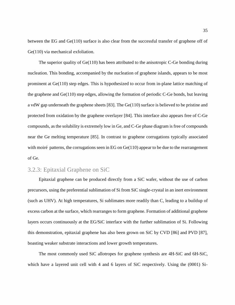
surface reconstruction, where R30° indicates the orientation relative to the underlying SiC. This
C-rich reconstruction is partially covalently bonded to the underlying SiC (Figure 3.2), exhibits an
in-plane structure distinct from the graphene honeycomb, and readily scatters charge carriers. The
C-terminated (0001̅) direction will also produce graphene, but without the consistent epitaxial
registry seen on the Si-terminated side.
Figure 3.2: The vertical electron density profile of EG on SiC(0001) interface derived from X-ray
standing wave constrained X-ray reflectivity. (a) 1.3 ML of graphene on SiC (b) 0 ML of graphene
on SiC. (Source: (a) adapted from Ref. [14] and (b) adapted from Ref. [88])
Through atomically thin layers of graphite were demonstrated using this approach as early
as 1998 [19]. These layers were not of sufficient quality to reproduce the charge transport
properties of graphene, when this approach was first demonstrated in UHV heating at 1600 K [19].
The obstacles to producing monolayer graphene primarily stemmed from the 3 layers of C in SiC
needed to produce the SiC(0001) (6√3 × 6√3)R30° reconstruction and each subsequent layer of
monolayer graphene. Quality of films has increased dramatically with reduced rates of Si
a b
37
sublimation under Si-rich atmosphere [89] or buffer gas such as Ar [90-92] at 1900 K. Both
approaches allot higher mobility of the C atoms at the surface, leading to the demonstration of near
continuous monolayers of EG on SiC.
3.3: Epitaxial Borophene
Recently, atomically thin sheets of boron (i.e., borophene) have been grown on silver
surfaces with structures distinct from known bulk boron allotropes [5,6]. Theory predicts the in-
plane B-B bonding (3 eV per B atom) to greatly exceed interactions with the substrate (100 meV
per B atom) and form a stable free-standing structure [49,93]. These sheets are evidently the
lightest known 2D metals [93-95], exhibiting anisotropic Dirac fermions and predictions of
relatively high Tc superconductivity which may elucidate the fundamental origins of metallicity
and correlated electron phenomena (e.g., superconductivity) in light elements [96,97]. Though the
interface between the borophene and the underlying silver has been predicted to play a role in
stabilizing borophene over more energetically favorable bulk structures [49,98], experimental
measurements of chemically resolved interface structure remain elusive.
3.3.1: Borophene R and D phases
Borophene deposited on silver shows at least 2 distinct lattice structures, one phase shows
a rectangular (R) 2D lattice structure, the other a diamond (D) (a.k.a. rhombic or face-centered
rectangular) 2D lattice structure, both are in registry with the underlying Ag(111) substrate [5,6].
Since initial experimental demonstrations of borophene, additional borophene structures have also
been reported, believe to be reconstructions of the Ag surface [99,100]. The STM derived lattice
shows the R phase can be described with lattice vectors |𝐚| = 5.0 Å and |𝐛| = 2.9 Å. Likewise the

38
D phase can be described with |𝐚| = |𝐛| = 4.6 Å and gamma = 142° [101], verified by low-energy
electron diffraction (LEED).
Figure 3.3: Borophene lattice and atomic structures. (a,b) STM topography images showing the
atomic-scale structures corresponding to the R and D phases. (f,g,h) LEED patterns acquired at 70
eV, corresponding to (c) borophene growth at 300 °C (predominantly R phase), and (h) borophene
growth at 400 °C (predominantly D phase). (STM images in a and b provided by A.J. Mannix)
STM imaging further reveals the R phase and D phase coexist on Ag(111) terraces, but as distinct
domains of borophene. Different ratios and relative orientations of these phases can be achieved
by modifying deposition temperature and atomic boron deposition rate {site unpublished LEED
paper}. These phases appear to exist only as monolayers, with the formation of bulk boron clusters
forming at high atomic boron surface coverage [6].
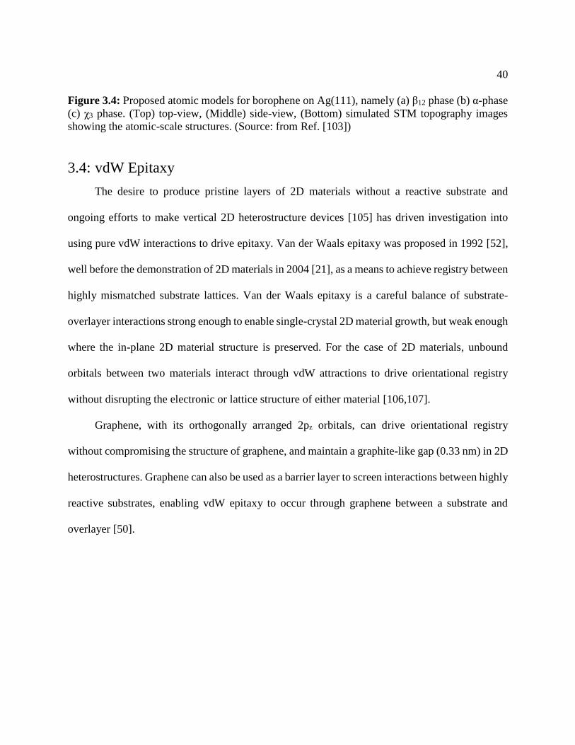
3.3.2: Atomic Models of Borophene
The atomic basis of borophene (i.e. the arrangement of boron atoms within the unit cell)
has not been measured directly. Density functional theory (DFT) calculations predict a large
degree of polymorphism in 2D boron structures [93], with at least two distinct models matching
the experimental STM data for the R phase of borophene. The first R phase model, called the α-
sheet [94,102] is a buckled triangular lattice, akin to graphene with the hexagonal honeycombs
completely filled. The vertically displaced atoms sitting one sitting 2.5 Å above the Ag(111)
surface and the other buckled an addition 0.8 Å outward to sit 3.3 Å above the Ag(111) surface

39
[6]. The second R phase model, called β12, features a highly-planar sheet of B atoms with a vacancy
concentration v = 1/6 of the triangular lattice sites. Alternatively, this can be thought of as a
graphene lattice, with ½ of the honeycombs filled with addition boron atoms. The D phase of
borophene is predicted from a slight modification to the β12 model, by using v = 1/5 to generate
the χ3 model, which achieves a diamond vacancy configuration [49]. Calculated STM data (Figure
3.4) from the α-phase, β12, and χ3 models closely match experiment, and both phases are reasonably
lattice matched to the Ag(111) substrate ~3.1% for α-phase and ~1% for β12 [100]. Recent review
articles by Zhang [103] and Mannix [104] acknowledge that current experimental results are
insufficient to unambiguously resolve the structure of borophene. To break the degeneracy of
proposed structure requires orthogonal structural descriptions as well as chemically specificity,
ideally with in situ measurements. To this end, XSW-XPS was employed as a chemically sensitive
vertical probe to resolve this structure, discussed in chapter 5.
40
Figure 3.4: Proposed atomic models for borophene on Ag(111), namely (a) β12 phase (b) α-phase
(c) χ3 phase. (Top) top-view, (Middle) side-view, (Bottom) simulated STM topography images
showing the atomic-scale structures. (Source: from Ref. [103])
3.4: vdW Epitaxy
The desire to produce pristine layers of 2D materials without a reactive substrate and
ongoing efforts to make vertical 2D heterostructure devices [105] has driven investigation into
using pure vdW interactions to drive epitaxy. Van der Waals epitaxy was proposed in 1992 [52],
well before the demonstration of 2D materials in 2004 [21], as a means to achieve registry between
highly mismatched substrate lattices. Van der Waals epitaxy is a careful balance of substrate-
overlayer interactions strong enough to enable single-crystal 2D material growth, but weak enough
where the in-plane 2D material structure is preserved. For the case of 2D materials, unbound
orbitals between two materials interact through vdW attractions to drive orientational registry
without disrupting the electronic or lattice structure of either material [106,107].
Graphene, with its orthogonally arranged 2pz orbitals, can drive orientational registry
without compromising the structure of graphene, and maintain a graphite-like gap (0.33 nm) in 2D
heterostructures. Graphene can also be used as a barrier layer to screen interactions between highly
reactive substrates, enabling vdW epitaxy to occur through graphene between a substrate and
overlayer [50].
41
Chapter 4: X-ray Characterization
Techniques
The challenge of deducing the chemically resolved vertical structure of 2D materials and
their interface bodes well for study through X-ray interface science. X-rays have already been used
extensively to study the structure of thin films and surface reconstructions. 2D materials represent
the ultimately limit of these structures, being single-atomic layer films. X-ray based techniques
(XSW, CTR, GIXS) are among the most precise vertical structure probes, allotting sub-Å
sensitivity. Owing to weak interactions with matter that enable the study of buried interface. This
dissertation demonstrates the use of synchrotron-based X-ray tools to solve the physics and
chemistry of new surface structures, with an emphasis on determining the interaction strength of
2D structures with a given substrate. Herein are the brief derivations of X-ray interactions with
matter relevant to understanding the work discussed in this document. Textbook descriptions of
the interactions of X-ray with matter are given in Warren [108] or Als-Nielsen and McMorrow
[109], and the specific case of hard X-ray photoelectron spectroscopy has been written by Woicik
[110].
4.1: Introduction to X-ray physics
4.1.1: X-ray interactions with matter
X-rays have been used to probe materials since their discovery by Wilhelm Conrad Röntgen
1895. Röntgen’s X-ray tube produced a small dose of X-rays over large-areas, which could
effectively distinguish between materials with vastly different adsorption coefficients (e.g. skin
and bone). High-intensity monochromatic X-rays enabled the determination of highly periodic
42
structures through X-ray scattering, including the celebrated discover of DNA helix structure
[111]. The development of highly brilliant monochromatic X-rays using third generation
synchrotrons enabled more exact chemical and structural information to be extracted from
materials, such as those presented in this work.
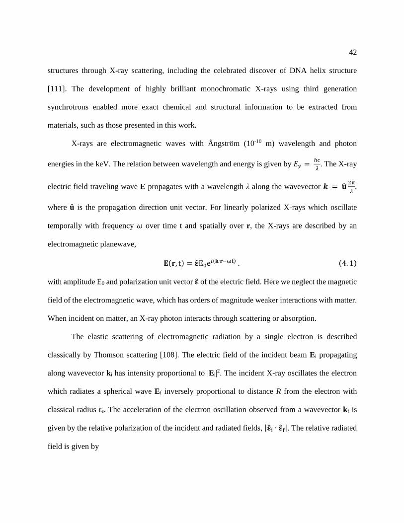
X-rays are electromagnetic waves with Ångström (10-10 m) wavelength and photon
energies in the keV. The relation between wavelength and energy is given by 𝐸𝛾 = ℎ𝑐
𝜆. The X-ray
electric field traveling wave E propagates with a wavelength λ along the wavevector 𝒌 = �̂�2π
𝜆,
where û is the propagation direction unit vector. For linearly polarized X-rays which oscillate
temporally with frequency 𝜔 over time t and spatially over r, the X-rays are described by an
electromagnetic planewave,
𝐄(𝐫, t) = �̂�E0e𝑖(𝐤∙𝐫−ωt) . (4. 1)
with amplitude E0 and polarization unit vector �̂� of the electric field. Here we neglect the magnetic
field of the electromagnetic wave, which has orders of magnitude weaker interactions with matter.
When incident on matter, an X-ray photon interacts through scattering or absorption.
The elastic scattering of electromagnetic radiation by a single electron is described
classically by Thomson scattering [108]. The electric field of the incident beam Ei propagating
along wavevector ki has intensity proportional to |Ei|2. The incident X-ray oscillates the electron
which radiates a spherical wave Ef inversely proportional to distance R from the electron with
classical radius re. The acceleration of the electron oscillation observed from a wavevector kf is
given by the relative polarization of the incident and radiated fields, |�̂�i ∙ �̂�f|. The relative radiated
field is given by
43
𝐄r
𝐄i= −
re
𝑅e𝑖(𝒌𝐟−𝒌𝐢)∙𝐫|�̂�i ∙ �̂�f| . (4. 2)
For simplicity kf – ki is defined as the momentum transfer vector q and |�̂�i ∙ �̂�f| as the polarizability
p. The polarization factor, P = |�̂�i ∙ �̂�f|2, depends on the geometry; for synchrotron experiments
with linearly polarized incident X-rays P = 1 in the vertical scattering plane (σ-polarized) and P =
cos2(2θ) in the horizontal scattering plane (π-polarized), while for an unpolarized lab source 𝑃 =
1+cos2 2𝜃
2. Where 2θ is the angle between kf and ki. The scattered intensity from a single electron
measured in X-ray experiments is therefore
𝐼 = |𝐄r|𝟐 = |𝐄i|𝟐
re2
𝑅2𝑃 . (4. 3)
Note that the phase information is lost when taking the complex conjugate |𝐄i|𝟐, this is the phase
problem in X-ray crystallography.
Now consider the atom made up of Z electrons described classically with a charge
distribution ρ(r). When considering X-ray scattering from atoms, only electrons need to be
considered because X-ray interactions with electron is ~107 greater than nuclei. The scattered field
is a superposition of the all scattering from all volume elements dr at positions r within ρ(r),
described by the atomic form factor,
𝑓0(𝐪) = ∫ 𝜌(𝐫)e𝑖𝐪∙𝐫 d𝒓 , (4. 4)
where two points separated by r have a q·r phase difference. The atomic form factor is a Fourier
transform of the charge distribution. When all scattering elements are in phase f(q = 0) = Z. With
increasing q, volume elements scatter out of phase and f(q → ∞) = 0.
44
Being bound to a nucleus, electrons in atoms cannot freely oscillate in response to an
electric field. This delayed response relative to the driving field is described by reduced scattering
length f′ and phase lag by if′′,
𝑓(𝐪, 𝜆) = 𝑓0(𝐪)+𝑓′(𝜆) + 𝑖𝑓′′(𝜆) , (4. 5)
known as the dispersion correction. This representation of the atomic form factor correctly
accounts for the binding between electrons and the atomic nucleus and will be used when
calculating X-ray interactions with a crystal in kinematical and ultimately dynamical diffraction
theory.
4.1.2: Kinematical scattering from a crystal
The scattering of a single atoms is not sufficient to be detected experimentally, considering
the interaction between the X-ray planewave and an ensemble of atoms enables Thomson
scattering theory to be extended to real materials. Solid crystalline materials can be modeled by
repeating a unit cell over set of lattice points to define 3D, 2D, or 1D structures. A crystal can be
defined mathematically as the convolution of the unit cell with the set of lattice points.
The interaction between X-rays and a set of lattice points is described by the weak-scattering
limit or kinematical approximation. Here, the influence of multiple scattering effects are neglected.
In general, scattering from a collection of atoms can be described by the form factor,
𝐹(𝐪, 𝜆)=∑ 𝑓j(𝐪, 𝜆)e𝑖𝐪∙𝐫𝐣
j
, (4. 6)
which is simply a sum over the atomic form factors 𝑓j(𝐪, 𝜆) over j atoms at positions rj. For the
case of crystal, the unit cell with vectors a, b, and c is repeated in a set of lattice points defined by
the vector 𝐑𝒏 = n1𝐚 + n2𝐛 + n3𝐜. The form factor for a crystal can therefore be described by
the product of unit cell structure factor with the lattice sum,
45
𝐹(𝐪, λ) = 𝐹u.c.(𝐪, 𝜆) ∑ e𝑖𝐪∙𝐑n
n
= ∑ 𝑓j(𝐪, 𝜆)e𝑖𝐪∙𝐫𝐣
j
∑ e𝑖𝐪∙𝐑n
n
, (4. 7)
for a unit cell with j atoms and n lattice points. Taking the geometric expansion of each component
of the lattice sum,
∑ e𝑖n𝑥 =
N−1
n=0
1 − 𝑒𝑖N𝑥
1 − 𝑒𝑖𝑥 , (4. 8)
it is apparent that for large values of N, typical of crystalline solids, the lattice sum will be near
unity unless q·Rn = 2π. This condition is fulfilled for a so-called reciprocal lattice set of vectors
𝐆ℎ𝑘𝑙 = ℎ𝐚∗ + 𝑘𝐛∗ + 𝑙𝐜∗ where 𝐆ℎ𝑘𝑙 · 𝐑n = 2π(ℎn1 + 𝑘n2 + 𝑙n3) and results in large values
for the structure factor and reflected intensity. For the limit of N , the reciprocal lattice defined
by Ghkl reduces to a set of δ-functions or so-called reciprocal lattice points. A reciprocal lattice
point Ghkl is the Fourier transform of the real space set of H = hkl lattice planes with spacing dhkl
where |𝐆ℎ𝑘𝑙| =2π
𝑑ℎ𝑘𝑙. The scalar geometry for the fulfillment of this condition is Braggs’ Law,
|𝑮𝐻| = |𝐪| =4π
sin (
2𝜃B
2) , (4. 9)
where the angle θB describes the angle of an incident and reflected plane wave relative the
sample surface plane. The vector geometry is therefore described by
𝑮𝐻 = 𝐪 = 𝐤𝐻 − 𝐤0 . (4. 10)
Using the kinematical approximation developed thus far, the reflected 𝐄𝑟 ∝ 𝐹(𝐪, λ), thus
the intensity at this condition is then given by 𝐼(𝐪, λ) = |𝐹(𝐪, λ)|2 when considering a perfectly
rigid single-crystal. Real crystals experience lattice vibrations originating primarily from thermal
vibrations of atoms. The instantaneous position of an atom is then given by 𝐑n + 𝐮n, where 𝐮n is

46
the displacement form the average atomic position. The time average the displacement, ⟨𝐮n⟩ = 0.
Evaluating the time-averaged structure factor with 𝐑n + 𝐮n results in
𝐼(𝐪, λ) = ⟨|𝐹(𝐪, λ)|2⟩ = |𝐹(𝐪, λ)|2𝑒−12
𝐪𝟐⋅⟨𝐮n𝟐 ⟩
, (4. 11)
where the exponential term is the Debye-Waller factor. The mean-squared amplitude ⟨|𝐮n𝟐|⟩
depends on the energy of the thermally excited phonons. For isotropic vibrations ⟨|𝐮n𝟐|⟩ = ⟨𝑢𝟐⟩
and the temperature dependence is given by a B-factor,
𝐵T =8𝜋2
3⟨𝑢𝟐⟩ .
The B-factor is a function of the temperature and empirically determined Debye temperature Θ of
the material [112,113].
4.1.3: Dynamical scattering from a perfect crystal
Dynamical diffraction theory is a more rigorous mathematical treatment of the interaction
between X-rays and matter which takes multiple scattering events into account. Herein is a
summary of Ewald-von Laue’s approach to solving dynamical scattering and impact on the
equations that govern X-ray interactions with matter, the details of the solution are described
initially in Batterman and Cole [114]. To reproduce the fine details of X-ray interaction with a
perfect crystal, Ewald-von Laue solved Maxwell’s equations for continuous electromagnetic
waves propagating in medium with a triply periodic complex relative permittivity. Using
appropriate boundary conditions, the solutions are wave fields that can be represented as Bloch
waves.
The crystal through which the X-rays are propagating can be thought of as a periodic
potential. This potential is described with a relative permittivity ϵr, which is a complex quantity
47
which describes how the polarization density P is influence by an electric field E within the
material. The polarization density 𝐏 = 𝜌(𝐫)𝐝 describes how the charge density ρ(r) is displaced
by a distance d. The permittivity is a measure of how resistance the material is to charge
displacement described by 𝐏 = ϵ0(ϵr − 1)𝐄, where ϵ0 is the permittivity of free space and ϵr −
1 = 𝜒𝑒 the electric susceptibility. For the case of X-rays interacting with matter, this susceptibility
can be represented as
𝜒e(𝒓) =𝜌(𝒓)𝐝
ϵ0𝐄= −
𝜌(𝒓)re𝜆2
π , (4. 12)
considering a sinusoidal field of amplitude E0 [114]. An inverse Fourier transform of the structure
factor results in the charge density 𝜌(𝐫) represented as a sum of structure factors in reciprocal
space,
𝜌(𝐫, 𝜆)=1
𝑉u.c.∑ 𝐹(𝐆𝐻, 𝜆)e−𝑖𝐆𝐻∙𝐫
𝐆𝐻
, (4. 13)
thus allowing the medium to be also be expressed as a sum of structure factors,
ϵr(𝒓) = 1 − Γ ∑ 𝐹(𝐆𝐻, 𝜆)e−𝑖𝐆𝐻∙𝐫
𝐆𝐻
, (4. 14)
with a scaling factor Γ = re𝜆2 π𝑉u.c.⁄ , where Vu.c. is the volume of the unit cell. The assumed
solution to Maxwell’s equations are planewaves described by Bloch functions with wavevector
GH and amplitude as a Fourier series. Maxwell’s equations,
∇ × 𝐄 = −𝜕𝐁
𝜕𝑡 ∇ × 𝐁 = ϵ0ϵr
𝜕𝐄
𝜕𝑡 , (4. 15)
can be solved using a choice of appropriate boundary conditions, the exact solution is described in
detail elsewhere for a perfect crystal [114] and for slightly distorted crystals [115,116], both of
which require appropriate choice of boundary conditions. Namely, the planewave solution must
48
be continuous inside and outside the crystal surface, this boundary condition is satisfied when for
every point on the surface (rs), such that
∑ 𝐄ie−2π𝑖𝐤i∙𝐫𝐬
i
= ∑ 𝐄fe−2π𝑖𝐤f∙𝐫𝐬
f
(4. 16)
for physically coupled waves at the Bragg condition, 𝐆𝐻 = 𝐤𝐻 − 𝐤0. When Maxwell’s equations
are solved with these constraints, the solution is a standing wave with energy dependent amplitude
and phase. It is common to describe the response of the standing wave solution using the
normalized parameter,
=
−2𝑏 (∆𝐸𝐸𝛾
) 𝑠𝑖𝑛2(B) +12𝐹0(1 − 𝑏)
|𝑃||𝑏|12√𝐹𝐻𝐹�̅�
, (4. 17)
which contains an offset from the geometrical Bragg energy ∆𝐸 = 𝐸𝛾 − 𝐸B. The equation for
can be similarly defined for an angular offset ∆ = − B from the Bragg angle [114]. For
convenience, 𝐹(𝐆𝐻, λ) has been separated into real 𝐹𝐻′ = 𝑓0(𝐆𝐻) + 𝑓′(λ) and imaginary 𝐹𝐻
′′ =
𝑖𝑓′′(λ) components such that 𝐹𝐻 = 𝐹𝐻′ + 𝑖𝐹𝐻
′′. The imaginary component of the H = 000 term of
the Fourier series 𝑖𝐹0′′(λ) is related to the linear absorption coefficient by 𝜇0 = 2𝜋 𝜆⁄ Γ𝐹0
′′. Simply
put, η is a complex quantity η′ + iη″ multiplied by ∆𝐸. The amplitude of the solution can be
understood as the ratio between incident and reflected beams,
E𝐻
E0= −
|𝑃|
𝑃|𝑏|
12 (𝜂 √𝜂2 − 1) √
𝐹𝐻
𝐹�̅� , (4. 18)
where the asymmetry factor 𝑏 = 0
𝐻⁄ is the ratio of the direction cosines of the incident γ0 and
reflected γH beams relative to the sample surface normal. Note that in Bragg (i.e. reflection)
geometry b is negative and for Laue (i.e. transmission) geometry b is positive. A useful substitution
49
for η is 1
2(𝑒𝑖𝜐 + 𝑒−𝑖𝜐) = cosh 𝜐 to such that (𝜂 √𝜂2 − 1) = 𝑒𝑖𝜐, which allows eq. 4.18 to be
recast in terms of phase,
E𝐻
E0= ∓|𝑏|
12𝑒𝑖𝜐√
𝐹𝐻
𝐹�̅� , (4. 19)
where the quantity υ is proportional to the relative phase between of the total field generated at the
Bragg condition. For a symmetric Bragg reflection crystal b = -1 and 𝐹𝐻 = 𝐹�̅�. The phase of EH
versus E0 shifts by π-radians when going from η′ = 1 (α branch) to η′ = -1 (β branch), which mark
the beginning and ending of the total Bragg reflection. The range of the total Bragg reflection can
be calculated from the different in energy at the α branch and the β branch, known as the Darwin
width E of the reflection where
E = 𝐸α − 𝐸β =𝐸𝛾|P|√𝐹𝐻
′ 𝐹�̅�′ + 𝐹0
′′2− 𝐹𝐻
′′𝐹�̅�′′
√|𝑏|sin2(B) , (4. 20)
the center of the reflection at η’ = 0 is offset from the kinematical approximation by
𝐸0 =𝐹0𝐸𝛾
2 sin2(B)
1 + |𝑏|
2|𝑏| . (4. 21)
4.1.4: X-ray photoexcitation
The excitation probability of an electron from initial ground state |𝑖⟩ to the final unbound
state |𝑓⟩ is expressed by the matrix element
𝑀𝑓𝑖 = 𝐸𝛾⟨𝑓|(−𝑖ℏ∇ ⋅ �̂�)e−𝑖𝐤⋅𝐫|𝑖⟩ , (4. 22)
for the absorption of a photon plane wave with electric field �̂�𝐸𝛾 and wavevector 𝐤 by an atom.
The quantity −iℏ∇ is the momentum operator. The differential absorption cross section of the
ejected photoelectron with wavevector 𝐤p can be written as
50
d𝜎(𝜃p, 𝜙p)
dΩ∝ |𝑀𝑓𝑖|
2 ,
from which the total cross section is calculated by integrating over the whole spatial angle Ω, with
spherical angles 𝜃p and 𝜙p relative to the incident beam polarization.
A multipole approximation of the matrix element 𝑀𝑓𝑖 is given by a Taylor series expansion
of the retardation factor e−𝑖𝐤⋅𝐫 = 1 − 𝑖𝐤 ⋅ 𝐫 −1
2(𝐤 ⋅ 𝐫)2 + ⋯, each term adds higher order
electromagnetic transitions. The first term (𝑀𝑓𝑖I ) gives the electric dipole; the second term (𝑀𝑓𝑖
II)
gives the electric quadrupole and magnetic dipole. For the dipole-quadrupole 2nd approximation,
the differential absorption is given by
d𝜎(𝜃p, 𝜙p)
dΩ∝ |𝑀𝑓𝑖
I |2
− 2ℜ[𝑀𝑓𝑖I ∗
𝑀𝑓𝑖II (𝐤)] . (4. 23)
the components of the second term are small compared to the first, so the |𝑀𝑓𝑖II|
2 terms are
neglected. This approximation is valid when the X-ray wavelength is considerably larger than the
electron-bound state orbital. For the case of a single X-ray beam with linearly polarized photons,
the general expression for differential absorption can be parameterized as
d𝜎
dΩ=
𝜎
4π{1 +
𝛽
2[3(�̂� ⋅ �̂�p)
2− 1] + [𝛿 + 𝛾(�̂� ⋅ �̂�p)
2] (�̂� ⋅ �̂�p)} , (4. 24)
where 𝛽 is the asymmetry factor from |𝑀𝑓𝑖I |
2; 𝛾 and 𝛿 are asymmetry factors from
2ℜ[𝑀𝑓𝑖I ∗
𝑀𝑓𝑖II (𝐤)]. These asymmetry factors depend on the atom, sub-shell, and photon energy and
can be found from simulated tables. The �̂� ⋅ �̂�p term introduces a forward and backward
asymmetry of photoemission depending on the direction of the incident photon. This non-dipolar
effect is significant at lower X-ray energies, particularly at the normal incidence reflection
geometry [117-119].

51
4.2: X-ray standing wave
X-ray spectroscopy imparts chemical specificity to Ångström-scale X-ray diffraction
measurements. Specifically, X-ray photoelectron spectroscopy (XPS) enhanced with X-ray
standing waves (XSW) has been instrument in resolving the interface structure of a myriad of 2D
materials on single-crystal surfaces [14,120,121]. With this capability, it is possible to distinguish
atoms on the surface from those in the bulk as well as the degree of bonding across a 2D material,
owing to the unique chemical signatures of these species seen by XPS and the distinct vertical
separation seen by XSW. For additional information, the reader is directed to reviews by Woodruff
[122] and Zegenhagen [123].
The XSW technique uses two coherently coupled X-ray plane waves, in this case generated
using Bragg diffraction, to produce specially resolved standing wave to periodically enhance X-
ray spectroscopic signals. The technique is used determine the position of native [124], dopant
[125,126], and surface atoms [124,127] with chemical sensitivity in/on a perfect single-crystal.
Critically XSW can be used to determine the precise spacing between chemical species, which in
a 2D structure, is indicative of the strength of interactions between layers.
4.2.1: X-ray excited photoelectron yield
The standing wave field comes from the interference of the incident plane wave,
𝐄0(𝐫, 𝑡) = �̂�0E0𝑒−𝑖 [𝐤0⋅𝐫−𝜔𝑡] , (4. 25)
and diffracted plane wave,
𝐄𝐻(𝐫, 𝑡) = �̂�𝐻E𝐻𝑒−𝑖 [𝐤𝐻⋅𝐫−𝜔𝑡] , (4. 26)
52
in a perfect single-crystal with the same time dependent frequency 𝜔𝑡. The standing wave field
𝐄T(𝐫, 𝑡) is sum of these coherent plane waves with a periodicity given by 𝒅𝐻 = 2𝜋 𝐤𝐻 − 𝒌0⁄ =
2π 𝐪⁄ . This sum of the complex e-field amplitudes is
𝐄T = [�̂�0E0𝑒−𝑖 𝐤0∙𝐫 + �̂�𝐻E𝐻𝑒−𝑖 𝐤𝐻∙𝐫]𝑒𝑖𝜔𝑡 , (4. 27)
which describes the total field of the standing wave. At the Bragg condition, 𝐪 = 𝐆𝐻, the
normalized intensity of the standing wave 𝐼(𝐫, 𝐸) = |𝐄T(𝐫, 𝑡)|2 E02⁄ is given by
|𝐄T|2
E02 = 1 + |
E𝐻
E0|
2
+ 2𝑃 |E𝐻
E0| ℜ {e−𝑖[𝐆𝐻∙𝐫−𝜐𝐸𝛾]} , (4. 28)
where the energy dependent standing wave phase 𝜐𝐸𝛾 is defined in eq. 4.19.
For standing wave excited photoemission, the position vector of the excited electron 𝐫 is
given by the displacement of the excited electron 𝐫e plus the position of the center of the atom 𝐫a.
The total photoexcitation matrix element is calculated using superposition of the incident and
reflected planewave by substituting eq. 4.27 into eq. 4.22, from which the matrix element
𝑀𝑓𝑖𝑇 (𝐫) = E0⟨𝑓|(−iℏ∇ ⋅ �̂�0)e−𝑖𝐤0⋅𝐫|𝑖⟩ + E𝐻⟨𝑓|(−iℏ∇ ⋅ �̂�𝐻)e−𝑖𝐤𝐻⋅𝐫|𝑖⟩ , (4. 29)
can be expressed as
𝑀𝑓𝑖𝑇 = E0e−𝑖𝒌𝟎⋅𝒓a
[𝑀𝑓𝑖(𝐤0, 𝐫e) +E𝐻
E0e−𝑖𝑮𝐻⋅𝒓a
𝑀𝑓𝑖(𝐤𝐻, 𝐫e)] , (4. 30)
by substituting 𝐫 = 𝐫a + 𝐫e. For a given polarization state, the normalized photoelectron cross
section d𝜎 dΩ⁄ ∝ |𝑀𝑓𝑖𝑇 (𝒓)|
2 which has the form of the standing wave intensity (eq. 4.28) where
|𝑀𝑓𝑖𝑇 |
2
E02 = 𝑆00 + 𝑆𝐻𝐻 |
E𝐻
E0|
2
+ 2 |E𝐻
E0| ℜ {𝑆0𝐻e−𝑖[𝐆𝐻⋅𝐫a−𝜐𝐸𝛾]} , (4. 31)
53
but with the addition of a set of angular emission parameters 𝑆00 = |𝑀𝑓𝑖(𝐤0, 𝐫e)|2, 𝑆𝐻𝐻 =
|𝑀𝑓𝑖(𝐤𝐻, 𝐫e)|2, and 𝑆0𝐻 = 𝑀𝑓𝑖(𝐤0, 𝐫e)∗𝑀𝑓𝑖(𝐤𝐻, 𝐫e). These modifications to the photoelectron
yield are from the photoelectron cross sections of the direct, scattered, and interfering X-ray
plane waves. These terms add the dipolar and quadripolar corrections to the photoemission
process. The 𝑆00 and 𝑆𝐻𝐻 are generally real, while the 𝑆0𝐻 is complex and results in a phase shift
𝜓 = |𝑆0𝐻|𝑒𝜓. The generalize yield function 𝑌𝐻T ∝ |𝑀𝑓𝑖
𝑇 (𝒓)|2 and is commonly written as
𝑌𝐻T = 1 + 𝑆R𝑅 + 2|𝑆I|√𝑅𝑓𝐻 cos [𝜓 − 2𝜋𝑃𝐻 − 𝜐𝐸𝛾
] (4. 32)
by defining
𝑅 = |E𝐻
E0|
2
, 𝑆R =𝑆𝐻𝐻
𝑆00 , 𝑆I =
𝑆0𝐻
𝑆00
and by introducing the coherent fraction fH and coherent position PH defined as
𝑓𝐻𝑒2π𝑖𝑃𝐻 = ∫ 𝜌(𝐫) 𝑒−𝑖𝐆𝐻∙𝐫d𝐫 (4. 33)
which are the amplitude and phase of the hkl Fourier component of the normalized atomic
distribution. The determination of the angular emission terms, have been calculated from the
matrix elements under the dipole quadrupole approximation of the photoemission cross section
[128]. The angular emission parameters become
𝑆00 =3𝜎D
4π[�̂�0 ⋅ �̂�p]
2[1 + 𝛾′(�̂�0 ⋅ �̂�p)]
𝑆𝐻𝐻 =3𝜎D
4π[�̂�𝐻 ⋅ �̂�p]
2[1 + 𝛾′(�̂�𝐻⋅�̂�p)] (4. 34)
𝑆0𝐻 =3𝜎D
4π[�̂�0 ⋅ �̂�p][�̂�𝐻 ⋅ �̂�p] [1 +
𝛾(�̂�0 ⋅ �̂�p) + 𝛾∗(�̂�𝐻 ⋅ �̂�p)
2] ,
54
where 𝜎D is the angularly integrated dipole cross section of photoelectron excitation, �̂�p is the
emitted photon electron wave, and the complex parameter 𝛾 = 𝛾′ + 𝑖γ′′= 𝛾0𝑒𝑖∆. The parameter
∆ = 𝛿d − 𝛿p is the difference partial phase shifts of the p- and d-state of the photoelectron, 𝛿d and
𝛿p can be determined from relativistic ab initio calculations [129,130].
4.2.2: Normal incidence Geometry
XSW performed at typical hard X-ray energies (e.g. Cu Kα, 8.03 keV) yield angular Darwin
widths of typically 10 – 50 microradians. To reach this theoretical width requires single-crystal
samples with mosaicity as a small fraction of Darwin width. At these energies, this restricts the
XSW measurement to highly perfect single-crystals (e.g. Ge, Si, a-TiO2, ).
Using 2𝜃 = 180° geometry minimizes the gradient of Braggs law 𝑑𝑙𝑎𝑚𝑏𝑑𝑎 d𝜃⁄ and
produces rocking curves with Darwin widths on the order of milliradians. This expanded Darwin
width allows elemental metals and other more imperfect single-crystals to be used to generate
standing waves. This geometry is referred to as both normal incidence XSW (NIXSW) and back-
reflection XSW (BRXSW). As is evident from Braggs’ law, achieving the normal incidence
geometry requires calculating an energy for a given substrate and reflection. The rocking curve is
scanned in energy rather than angle to maintain the �̂�0 ≈ −�̂�𝐻 condition. Maintaining this
geometry allows considerable simplification of the angular emission parameters, eq. 4.34. For the
case of an s→p transition with σ-polarization and the spectrometer perpendicular to �̂�0 + �̂�𝐻, the
non-dipolar effects angular photoemission cross section terms, eq. 4.32, can be simplified to
𝑆R =1 + 𝛾′ cos 𝜃p sin 𝜃
1 − 𝛾′ cos 𝜃p sin 𝜃 , 𝑆I =
1 + 𝑖𝛾′′ cos 𝜃p sin 𝜃
1 − 𝛾′ cos 𝜃p sin 𝜃, (4. 35)
where 𝜃p = 𝐆𝐻 ∡ �̂�p. In the NIXSW geometry, sin 𝜃 = 1 and the equations further simplify to
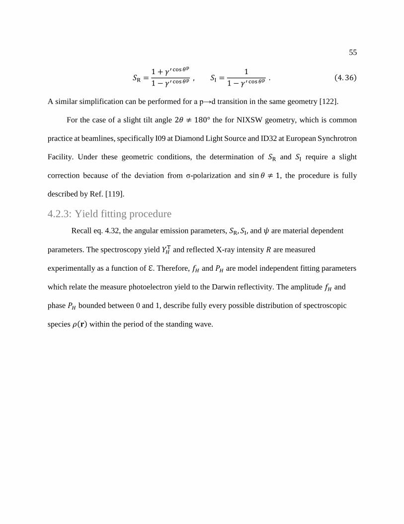
55
𝑆R =1 + 𝛾′ cos 𝜃p
1 − 𝛾′ cos 𝜃p , 𝑆I =1
1 − 𝛾′ cos 𝜃p . (4. 36)
A similar simplification can be performed for a p→d transition in the same geometry [122].
For the case of a slight tilt angle 2𝜃 ≠ 180° the for NIXSW geometry, which is common
practice at beamlines, specifically I09 at Diamond Light Source and ID32 at European Synchrotron
Facility. Under these geometric conditions, the determination of 𝑆R and 𝑆I require a slight
correction because of the deviation from σ-polarization and sin 𝜃 ≠ 1, the procedure is fully
described by Ref. [119].
4.2.3: Yield fitting procedure
Recall eq. 4.32, the angular emission parameters, 𝑆R, 𝑆I, and 𝜓 are material dependent
parameters. The spectroscopy yield 𝑌𝐻T and reflected X-ray intensity 𝑅 are measured
experimentally as a function of ℇ. Therefore, 𝑓𝐻 and 𝑃𝐻 are model independent fitting parameters
which relate the measure photoelectron yield to the Darwin reflectivity. The amplitude 𝑓𝐻 and
phase 𝑃𝐻 bounded between 0 and 1, describe fully every possible distribution of spectroscopic
species 𝜌(𝐫) within the period of the standing wave.
56
Figure 4.1: Simulated X-ray standing wave measurement of borophene (top) schematic showing
position of boron atoms (red) relative to Ag(111) single-crystal (grey) and the standing wave
(blue). (bottom) Simulated yield for coherent positions PH of distinct boron atoms buckled (left)
and planar (right) borophene assuming a coherent fraction fH = 1 and where the plane defined by
the center of Ag atoms gives PH = 0 = 1. The dotted line indicates the energy where the phase of
the standing wave, ψ = π. (Source: adapted from Ref. [103])
The coherent fraction is a measure of the distribution of 𝜌(𝐫), while the coherent position is
a measure of the average position of the distribution. To more precisely interpret atomic structure
from measured coherent fractions and positions, solve eq. 4.33 along the H = hkl direction of the
standing wave for atoms with distribution 𝜌(𝐫). For the simple case of a distribution of atomic
species (s),
ℱ𝐻s = 𝑓𝐻
N𝑒2π𝑖𝑃𝐻N
=1
𝐶n∑ 𝑐n𝑒2π𝑖𝑃𝐻
n
N
n=1
, (4. 37)
57
where the distribution is comprised of N sites with coherent positions 𝑃𝐻n and a occupation fraction
𝑐n < 1 of each site. The solution to eq. 4.37 can be found by summing complex vectors with
magnitude 𝑓𝐻n and phase angle 2π𝑃𝐻
n in the complex plane. Simulated XSW yields for proposed
atomic configurations of borophene on Ag(111) are shown in Figure 4.1.
XSW measurements taken at a set of at least three linearly independent H = hkl can be
used to determine the location of atoms relative to the 3D bulk single-crystal [131,132]. Where by
Fourier reconstruction methods [133], each 𝑓𝐻 and 𝑃𝐻 contributed a Fourier component along
which interfere to reveal the atomic positions of the measured atoms relative to the bulk single-
crystal unit cell.
4.3: Crystal Truncation Rod
The crystal truncation technique uses interference between adlayers and a perfect single-
crystal substrate to solve the structure of the interface. These interfaces often play a pivotal role in
understanding the mechanisms behind epitaxial registry of monolayers on single-crystals. This
measurement was the first direct structural measurement of covalent-like bonding present at the
EG/SiC [134] interface and revealed the formation of a wetting AgxSi1-x alloy layer at the
Ag/Si(111) interface which seeded Ag(111) epitaxy [135]. The CTR technique helps distinguish
structures with many chemically similar layers of material.
4.3.1: Kinematical Scattering from a surface
Kinematical scattering for an infinite bulk crystal results in a structure factor F with
scattering occurring at the 𝑮𝐻 = 𝐪 = 𝐤𝐻 − 𝐤0 Laue condition. The cleavage of the perfect crystal
reduces the lattice to a finite size along the surface normal of the truncated crystal, which in
reciprocal lattice stretches the points 𝑮𝐻 along the surface normal resulting in the crystal truncation
58
rods. The truncation of single-crystal surface is mathematically represented by the lattice sum
along c,
𝐹CTR(𝐪) = 𝐹ℎ𝑘(𝐪) ∑ 𝑒𝑖𝐪⋅[n𝐜]
0
n=−∞
𝑒−n𝛽 = 𝐹ℎ𝑘(𝐪)1
1 − 𝑒𝑖𝐪⋅𝐜−𝛽 , (4. 38)
where the absorption parameter is given by 𝛽 = 𝜇 sin 𝜃⁄ for one atomic plane along the surface
normal. 𝐹CTR(𝐪) depends on the precise truncation of the crystal surface, which then modulated
by interference with surface adlayers. For an adlayer with in-plane structure factor 𝐹ℎ𝑘(𝐪) and
which deviates from bulk plane-spacing by a fraction 𝑧0,
𝐹T(𝐪) = 𝐹CTR(𝐪) + 𝐹ℎ𝑘(𝐪)𝑒𝑖𝐪⋅[(1+𝑧0)𝒄]−𝛽 . (4. 39)
Recalling the derivations of the kinematical approximation, the measured intensity of such a
surface is
𝐼(𝐪) = 𝐹T(𝐪)𝑒−12
𝐪𝟐⋅⟨𝐮n𝟐 ⟩
. (4. 40)
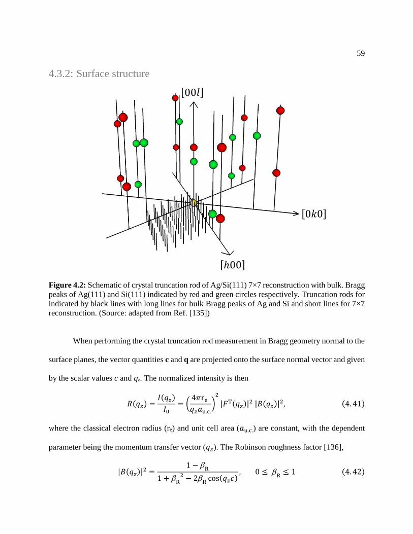
59
4.3.2: Surface structure
Figure 4.2: Schematic of crystal truncation rod of Ag/Si(111) 7×7 reconstruction with bulk. Bragg
peaks of Ag(111) and Si(111) indicated by red and green circles respectively. Truncation rods for
indicated by black lines with long lines for bulk Bragg peaks of Ag and Si and short lines for 7×7
reconstruction. (Source: adapted from Ref. [135])
When performing the crystal truncation rod measurement in Bragg geometry normal to the
surface planes, the vector quantities c and q are projected onto the surface normal vector and given
by the scalar values c and qz. The normalized intensity is then
𝑅(𝑞𝑧) =𝐼(𝑞𝑧)
𝐼0= (
4𝜋re
𝑞𝑧𝑎u.c.)
2
|𝐹T(𝑞𝑧)|2 |𝐵(𝑞𝑧)|2, (4. 41)
where the classical electron radius (re) and unit cell area (𝑎u.c.) are constant, with the dependent
parameter being the momentum transfer vector (𝑞𝑧). The Robinson roughness factor [136],
|𝐵(𝑞𝑧)|2 =1 −
R
1 + R
2 − 2R
cos(𝑞𝑧𝑐), 0 ≤
R≤ 1 (4. 42)
[00𝑙]
[0𝑘0]
[ℎ00]
60
accounts for the impact of inhomogeneity on the surface (e.g. step edges) on the measured specular
reflectivity. This measured reflectivity can be rewritten using a piecewise function to describe 𝐹T,
𝑅(𝑞𝑧) = (4𝜋𝑟e
𝑞𝑧𝑎u.c)
2
|𝐹u.c.(𝑞𝑧)𝐹CTR(𝑞𝑧) + 𝐹s(𝑞𝑧) + 𝐹v(𝑞𝑧)|2
|𝐵(𝑞𝑧)|2, (4. 43)
where contributions from the bulk crystal substrate, the topmost bulk-like crystal planes, and
overlayers are given by 𝐹u.c., 𝐹s, and 𝐹v, respectively. These are each described with a discrete or
infinite sum of m lattice planes,
𝐹(𝑞𝑧) = ∑ Θm𝑓m𝑎(𝑞𝑧)𝑒𝑖𝑞𝑧𝑧m
m
𝑒−12
(𝑞𝑧𝑢m)2(4. 44)
measured normal to the crystal surface, where each lattice plane is calculated from the average
height relative to the surface, zm, fractional monolayer occupancy, Θm, and distribution width, um.
The maximum achievable real-space resolution of the Fourier transform is described by the
Nyquist-Shannon Theorem. This value, given by 1/qmax, was added in quadrature to u.
The methodology to collect CTR reflectivity data using a hybrid photon-counting (HPC)
has been written by Fenter [137,138]. Using model-dependent statistical analysis, the terms z, Θ,
and u are refined until the calculated reflectivity matches the experimentally measured reflectivity.
The modeling tool used for this thesis work is least-squares analysis by implementing the Fienup
algorithm [139] to generate electron density profiles.
4.4: Grazing incidence X-ray diffraction
Grazing incidence X-ray diffraction (GIXD) diffraction is a powerful tool for determining
the size, shape, and orientation of nanostructures on surfaces. Through the generation of an
evanescent wave on the surface, X-rays intensity decreases exponentially with depth, allotting X-
ray techniques with heightened surface sensitivity. These techniques are commonly applied to 2D
materials to achieve measurable diffracted intensity.

61
4.4.1: Intensity and grazing angles
GIXD gains surface sensitivity the from low penetration into bulk and enhanced electric
field at surface achieved near the total external reflection condition. The refractive index of X-rays
𝑛 = 1 − 𝛿 − 𝑖𝛽, being slightly less than unity, leads to the total external reflection of an incident
X-ray beam at angles 𝛼i below the critical angle 𝛼c < √2𝛿. Though all X-rays are reflected below
𝛼c, the X-ray E-field penetrates the surface with an exponentially decaying function known as the
evanescent wave. The depth of penetration is given by
𝑍 =𝜆
2√2π (√𝛼i2 − 𝛼c
2 + 4𝛽2 + 𝛼c2 − 𝛼i
2)12
. (4. 45)
A second consequence of the evanescent wave effect is the factor of four increase in E-
field intensity at 𝛼𝑖 = 𝛼𝑐. This enhanced E-field effect enhances in-plane scattering from surface
structures, making it an optimal geometry for 2D crystal structure determination. Consider a crystal
substrate with in-plane vectors h and k with the surface normal l. The structure factor 𝐹(𝑞) is
smeared along the surface normal l, so the determination of integrated intensity requires integrating
the entire rod. A practical approach is use discrete portion of the rod qz = 0 to acquire planar
intensity cross sections. The derivation of the in-plane structure factor 𝐹ℎ𝑘 follows the derivation
of kinematical diffraction theory with l = 0,
𝐹ℎ𝑘(𝑞) = 𝑓𝑎(𝑞) | ∑ e𝑖(ℎ𝐚∗+𝑘𝐛∗)∙𝐫m𝑒⟨[𝑖𝐪⋅𝐮𝐦]⟩
M
m=1
|
2
. (4. 46)
Extracting the structure factor 𝐹ℎ𝑘 from scattered intensity requires additional factors to account
for the 2D experimental geometry and deviations from ideal kinematical scattering theory. The
Lorentz polarization factor 𝐿𝑃 = 𝑃𝐻 sin 2𝜃B⁄ accounts for the polarization of the incident beam
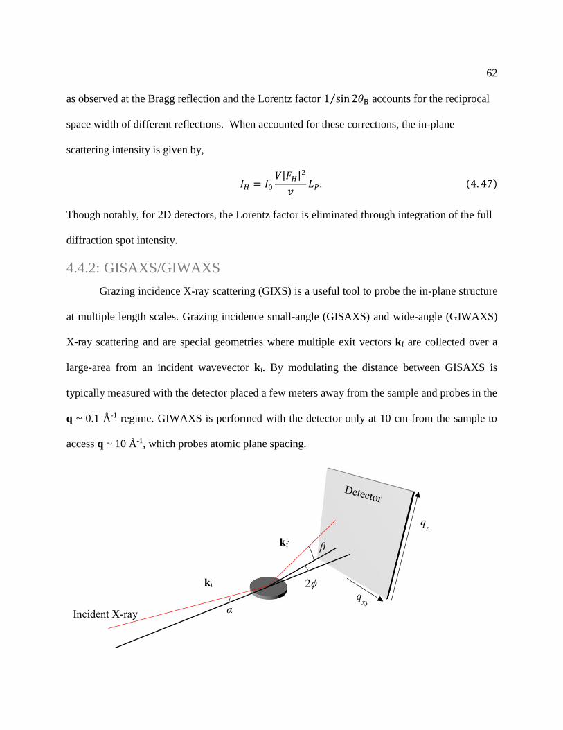
62
as observed at the Bragg reflection and the Lorentz factor 1 sin 2𝜃B⁄ accounts for the reciprocal
space width of different reflections. When accounted for these corrections, the in-plane
scattering intensity is given by,
𝐼𝐻 = 𝐼0
𝑉|𝐹𝐻|2
𝑣𝐿𝑃. (4. 47)
Though notably, for 2D detectors, the Lorentz factor is eliminated through integration of the full
diffraction spot intensity.
4.4.2: GISAXS/GIWAXS
Grazing incidence X-ray scattering (GIXS) is a useful tool to probe the in-plane structure
at multiple length scales. Grazing incidence small-angle (GISAXS) and wide-angle (GIWAXS)
X-ray scattering and are special geometries where multiple exit vectors kf are collected over a
large-area from an incident wavevector ki. By modulating the distance between GISAXS is
typically measured with the detector placed a few meters away from the sample and probes in the
q ~ 0.1 Å-1 regime. GIWAXS is performed with the detector only at 10 cm from the sample to
access q ~ 10 Å-1, which probes atomic plane spacing.
α
ki
β
2
kf
qxy
qz
Incident X-ray
63
Figure 4.3: GIXS geometric setup showing incident x-ray with vector ki, scattered vector kf,
incident angle α, scattered vertical angle β and horizontal angle 2.
4.5: X-ray Photoelectron Spectroscopy
X-ray Photoelectron Spectroscopy (XPS) is a highly surface sensitive tool for non-
destructive chemical state analysis of a surface at parts per thousand atomic
concentrations. [109]
4.5.1: X-ray Photoelectron Spectroscopy
X-ray Photoelectron spectroscopy (XPS) is typically performed under ultra-high vacuum (<
10-7 mbar) to prevent air absorption of emitted photoelectrons with nanometer mean free paths in
ambient. Though at this time, there are ongoing efforts to develop ambient-pressure XPS to study
UHV-incompatible systems. Energy-dispersive spectrometers measure the quantity of ejected
photoelectrons as a function of Ek. Electron optics within the spectrometer allow electrons in a
finite Ek window (pass energy) to reach the photoelectron detector, which is scanned over a user-
defined energy region. Ek is commonly converted to Eb and put on a reverse linear scale. A kinetic
energy calibration is performed by setting the measured spectra to a known parameter (e.g.
avaricious carbon peak or fermi energy).
4.5.2: Photoemission Physics
Electrons in a material occupy discrete energy states described by the dispersion relation for
which the interaction between wavevector qv of the electron and the material results in
characteristics binding energies (Eb). Photoelectric absorption can occur in a material when an
incident X-ray has an energy (Eγ) which exceeds the minimum energy required to excite the most

64
weakly bonded electron into vacuum, this is the work function (ΦA) of the material. As Eγ
increases, tightly bonded core-shell electrons are excited into vacuum with kinetic energy
𝐸k =ℏ2𝐪v
2
2𝑚= 𝐸𝛾 − (𝐸b + ΦA) . (4. 48)
This approach enables the determination of Eb which is sufficient to deduce the chemical
composition of atoms at a surface. This is the basis of X-ray photoelectron spectroscopy (XPS).
Local chemistry induces subtle changes in electron binding energy, thus XPS is commonly
used as a means to distinguish different chemical states [140]. An example of this is spin-orbit
interactions, which result in doublet peak (e.g. 3d3/2 and 3d5/2) for all orbitals with distinct angular
momentum (i.e. not s). Core-level shifts also reflects the valence state of the electron, which is
most commonly analyzed through comparison to a compound specific elemental library [140].
Core-level shifts can also reflect changes to the electronic structure, including band-bending [141]
and doping [82,142]. The width of the measured peak is defined by the full width half-maximum
∆E, and is a convolution of chemical-state effects with the intrinsic energy width Γ of the peak,
the X-ray line width, and the analyzer resolution. The intrinsic peak broadening is an example of
the uncertainty principle in time-energy space, Γ =ℎ
𝜏 where h is Planck’s constant and τ is the
core-hole lifetime [143]. The depletion of electrons near the Fermi energy also leads to apparent
peak broadening from core-shifting due to increased nuclear charge. This effect is evident from an
asymmetric broadening of the low KE tail of the peak [144].
4.5.3: Composition Analysis
Analysis of the XPS peak shape and intensities requires a quantum mechanical treatment
to extract quantitative chemical state composition within the measured film. A number of
simplified models for the quantum mechanical description of XPS to enable extracting quantitative

65
information. In practice, determining the photoabsorption coefficients is done either with
experimentally verified model calculations. Scofield has calculated photoionization cross sections
for neutral atoms ranging from 1 keV to 1500 keV [145].
The substrate—overlayer model [146-148] describe the influence of thin (< 29 Å)
overlayers on measured XPS peak intensity. The s-o model is based upon effective attenuation
length (EAL) calculations,
𝐸𝐴𝐿 = − {cos 𝛼𝑑ln[(𝑧, 𝛼)]
𝑑𝑧} , (4. 49)
which provides a measurement of the probability of inelastic scattering for detected photoelectrons
as a function of depth z and electron emission angle α. The precise calculation of EAL differs
between models and is the primary source of uncertainty. Nonetheless, reasonable estimates of the
overlayer thickness t can be determined by comparing these theoretically predicated EALSs to
their experimentally derived values.
EAL theories by Powell and Tanuma [149,150] and Gries [151] have been constructed
into a comprehensive NIST database [152] and companion software package to calculate EALs
using predictive models for electron kinetic energies ranging from 50 eV to 2,000 eV for a wide
range of elements and compounds. The NIST database calculates the inelastic mean free path [153]
(IMFP) and transport mean free path [154,155] (TMFP) which provide the length at which
intensity is reduced to 1/e due to inelastic and elastic scattering of photoelectrons. For a given
material, the IMFP has an electron kinetic energy dependence described by the Bethe
equation[153]
𝜆i =𝐸
𝐸p [𝛽 ln(𝛾𝐸) − (𝐶𝐸) + (
𝐷𝐸2)]
(4. 50)

66
where E is the electron energy and Ep is the bulk plasmon energy. The parameters β, γ, C, and D
depend on the valence, density, atomic weight, and bandgap of the material, described in detail by
Tanuma [149]. TMFP describes the frequency at which electrons undergo elastic scattering events
by
𝜆t =1
N𝜎t
(4. 51)
Which depends on the so-called transport cross section (σt) of the atom. These σt have been
calculated for a variety of atomic potential models [154]. EALs as a function of λi and λt for a
wide range of materials with α ranging from 0° to 50° and electron energies between 61 eV and
2016 eV were fit by
𝐿 = 𝜆i (1 −𝐵𝜆i
𝜆i + 𝜆t) , (4. 52)
where B = 0.735 is a linear fit parameter determined by Jablonski [154].
Powell and Tasneem [148] describe two methods for relating film thickness to effective
attenuation length for an overlayer (v) and substrate (s) taken at X-ray incidence angle θ and
electron emission angle α using measured intensity ratios. Both methods consider elastic-scattering
effects to be negligible. The first method uses the difference in peak intensity of the substrate signal
𝐼s for a pure substrate 𝐼0s compared to the intensity attenuated with an overlayer 𝐼𝑡
s to relate EAL
to overlayer thickness by
𝐿 = 𝑡
(ln𝐼0s − ln𝐼𝑡
s)cos 𝛼. (4. 53)
The second method additionally uses the peak intensities of the overlayer 𝐼𝑣 for a very
thick overlayer 𝐼∞v and for an overlayer of a given thickness 𝐼𝑡
v to determine the ratios of peak
intensities for overlayer and substrate. The thickness dependent EAL is given by

67
𝐿 = 𝑡 [(𝐹 +𝐼𝑡
v 𝐼𝑡s⁄
𝐼∞v 𝐼0
s⁄) cos 𝛼]
−1
, (4. 54)
where F depends on the photoelectron energy as
𝐹 =𝑒−𝑡 𝐿v cos 𝛼⁄
𝑒−𝑡 𝐿s cos 𝛼⁄, (4. 55)
where Lv and Ls are EALs for the overlayer and substrate respectively through the film.
4.6: Other Techniques
4.6.1: X-ray Fluorescence
When an X-ray of sufficient energy excites a core-shell electron into vacuum level, the
atom relaxes by filling the core-hole with a valence electron accompanied by the ejection of a
photon (fluorescence) or another electron (auger). Measuring photons emitted is the basis of X-
ray fluorescence (XRF), which provides quantitative information about the elemental composition
and coverage of material. Analyzing the characteristic energies at which photons are emitted gives
the atomic composition of a sample at sub-monolayer concentrations. Measuring relative phonon
intensities can extract the effective coverage of the atomic species, provided geometry, XRF
emission efficiency, and absorption effects are properly accounted for [156].
4.6.2: Low-Energy Electron Diffraction
The low-energy electron diffraction (LEED) technique, much like in-plane X-ray diffraction,
generates a reciprocal space lattice by the diffraction of a collimated beam of electrons (20-200
eV). The low electron energy makes LEED sensitive to the top 5-10 Å of a surface, owing to a
large interaction cross section ~1 Å2, over 106 times greater than X-rays with matter. The downside
of the strong interaction between electrons and matter is that the kinematic approximation does
not hold for LEED, so any analysis based on LEED spot intensities [157] requires the

68
implementation of dynamical diffraction theory. Herein, LEED is used as a qualitative in situ
monitor the evolution of surface structures, whereas X-ray and other surface science techniques
are used for structure determination.

69
Chapter 5: B/Ag(111) Interface
5.1: Abstract
Atomically thin two-dimensional (2D) materials exhibit superlative properties dictated by
their intralayer atomic structure, which is typically derived from a limited number of
thermodynamically stable bulk layered crystals (e.g., graphene from graphite). The growth of
entirely synthetic 2D crystals – those with no corresponding bulk allotrope – would circumvent
this dependence upon bulk thermodynamics and substantially expand the phase space available for
structure-property engineering of 2D materials. However, it remains unclear if synthetic 2D
materials can exist as structurally and chemically distinct layers anchored by van der Waals (vdW)
forces, as opposed to strongly bound adlayers. Here, we show that atomically thin sheets of boron
(i.e., borophene) grown on the Ag(111) surface exhibit a vdW-like structure without a
corresponding bulk allotrope. Using X-ray standing wave (XSW)-excited X-ray photoelectron
spectroscopy (XPS), the positions of boron in multiple chemical states are resolved with sub-
Ångström spatial resolution, revealing that the borophene forms a single planar layer that is 2.4 Å
above the unreconstructed Ag surface. Moreover, our results reveal that multiple borophene phases
exhibit these characteristics, denoting a unique form of polymorphism consistent with recent
predictions. This observation of synthetic borophene as chemically discrete from the growth
substrate suggests that it is possible to engineer a much wider variety of 2D materials than those
accessible through bulk layered crystal structures.
5.2: Introduction
Boron can form highly coordinated networks built around a motif of unconventional
covalent bonds, which are frequently delocalized about three or more atoms [158,159]. Recently,
70
2D sheets of borophene have been synthesized by depositing pure boron on atomically flat
Ag(111) substrates under ultra-high vacuum (UHV) conditions [5,6], as illustrated in Figure 5.1a.
These structures are distinct from conventional atomically thin 2D materials, which are derived
from thermodynamically stable bulk layered crystals [160] (e.g., graphene from graphite) and
exhibit superlative properties [30,161,162] dictated by their intralayer atomic structure. In contrast,
borophene is believed to exhibit a planar form similar to laterally fused nanoscale boron clusters
[49,94,159,163,164], with a number of predicted, energetically similar vacancy superlattices
characterized by a vacancy concentration vx [93,165]. Specifically, the v1/6 and v1/5 structure
models—shown in Figure 5.1b,c respectively—have been proposed for borophene on the Ag(111)
surface [5,49,101]. These structures should exhibit distinct chemical signatures due to the
differences in B-B coordination numbers (labeled in the inset models), with the v1/6 structure
demonstrating a 2:2:1 ratio of 4-fold, 5-fold, and 6-fold coordination and the v1/5 showing a 1:1
ratio of 4-fold and 5-fold coordination. Despite the differences in in-plane structure between the
two models, the predicted vertical separation from the Ag(111) substrate is 2.4 Å in both cases –
a value similar to the gap between graphene [74,166] or hexagonal boron nitride [120] and metal
growth substrates. Because the out-of-plane structure of borophene with respect to the underlying
Ag(111) substrate has not been directly quantified, it remains experimentally unclear whether
borophene is comprised of weakly bound sheets in a planar [5,49,101] or buckled [6] morphology
or as a strongly chemisorbed layer. Here, we characterize the structure of borophene under pristine
UHV conditions with XSW-excited XPS [122,167], which measures the distribution of atoms
relative to the substrate lattice with both sub-Å spatial resolution and chemical state specificity.
Independent of the specific in-plane structure, borophene is found to exist as a single, atomically

71
flat layer (i.e., not buckled) that is separated from the underlying Ag(111) substrate by a
noncovalent gap of 2.4 Å with no evident B-Ag primary bonding. This work thus experimentally
demonstrates that borophene is a synthetic, elemental 2D material with no bulk analogue.
Figure 5.1: Borophene synthesis and atomic structures. (a) Schematic of borophene growth. (b,c)
Atomic models of Ag(111)-supported borophene in the v1/6 and v1/5 structures, respectively. The
enlarged models show the LEED derived rectangular (R) and diamond (D) 2D unit cells over each
phase with the boron atomic coordination numbers labeled. (d,e) STM topography images showing
the atomic-scale structures corresponding to the R and D phases. (f,g,h) LEED patterns acquired
at 70 eV, corresponding to (f) clean Ag(111), (g) borophene growth at 300 °C (predominantly R
phase), and (h) borophene growth at 400 °C (predominantly D phase). (STM images in a and b
provided by A.J. Mannix)
Two structural phases of borophene have been observed experimentally via scanning
tunneling microscopy (STM) and low-energy electron diffraction (LEED): a primitive rectangular
phase [R phase; (Figure 5.1d)] and a diamond phase [D phase; (Figure 5.1e)] [5,6], which are
expected to match the computationally predicted v1/6 and v1/5 structures, respectively
[5,100,101,168]. The phase of borophene is determined by the boron deposition rate and the
Ag(111) substrate temperature during growth [5,6].
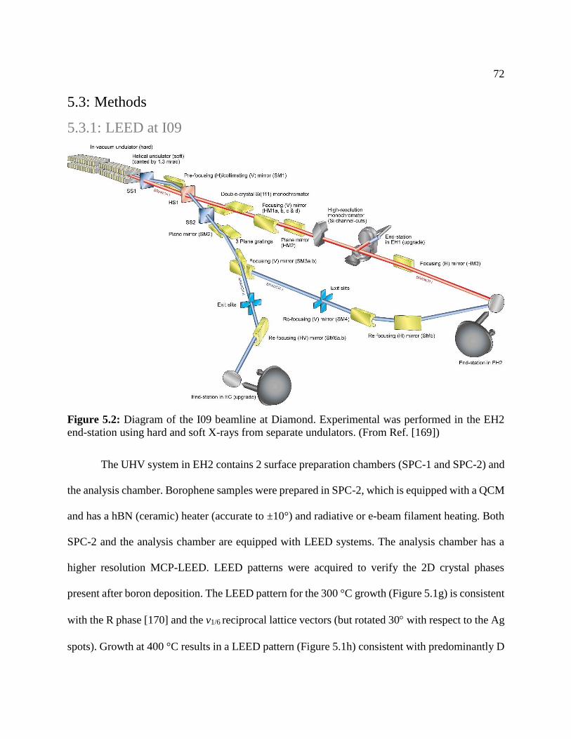
72
5.3: Methods
5.3.1: LEED at I09
Figure 5.2: Diagram of the I09 beamline at Diamond. Experimental was performed in the EH2
end-station using hard and soft X-rays from separate undulators. (From Ref. [169])
The UHV system in EH2 contains 2 surface preparation chambers (SPC-1 and SPC-2) and
the analysis chamber. Borophene samples were prepared in SPC-2, which is equipped with a QCM
and has a hBN (ceramic) heater (accurate to ±10°) and radiative or e-beam filament heating. Both
SPC-2 and the analysis chamber are equipped with LEED systems. The analysis chamber has a
higher resolution MCP-LEED. LEED patterns were acquired to verify the 2D crystal phases
present after boron deposition. The LEED pattern for the 300 °C growth (Figure 5.1g) is consistent
with the R phase [170] and the v1/6 reciprocal lattice vectors (but rotated 30 with respect to the Ag
spots). Growth at 400 °C results in a LEED pattern (Figure 5.1h) consistent with predominantly D
73
phase [6], which can be explained by a combination of the reciprocal lattice vectors of both the
v1/5 and v1/6 models. As will be shown later by XPS, the 300 °C borophene is ~90% R phase and
the 400 °C borophene is ~90% D phase.
5.3.2: X-ray at I09
To analyze the character of the bonds at the B/Ag(111) interface, we probed the chemical
identity of the R and D phases in situ using XPS and XSW at the Diamond Light Source I09
beamline, which is capable of providing both soft (100 – 2100 eV) and hard X-rays (2.1 – 20 keV)
at the same spot on the sample from two separate undulators. Soft X-rays used a defocused beam
size of 300 x 300 μm2. Hard X-rays were focused down to 40% of the original 300 x 300 μm2
beam size. XSW measurements were acquired using hard X-rays in a back-reflection geometry
(i.e., θB ≲ 90°) to maximize the B 1s yield and minimize the effect of Ag(111) mosaicity [122].
An incident beam energy of 𝐸 = 2.629 keV was selected by tuning the first harmonic of the I09
undulator and the Si(111) double-crystal monochromator. An incident beam energy of 𝐸 = 2.629
keV was selected by tuning the first harmonic of the I09 undulator and the Si(111) double-crystal
monochromator to measure Ag{111}. At this energy, the incident beam full-width half-maximum
(FWHM) bandwidth was 𝐸 = 0.36 eV. The undulator was tuned to 3.06 keV to collect Ag(020).
The third harmonic was tuned to 4.29 keV to access the Ag(022). The Bragg diffracted beam in
this near back-reflection geometry was measured by a CCD camera pointed at a Cu plate coated
with YAG fluorescent powder. We measured O 1s, Ag 3d, C 1s, B 1s, and survey XPS spectra at
variable soft X-ray energies, the FWHM bandwidth was 𝐸 = 90 meV at 500 eV. No evidence
of other elements (namely, oxygen or carbon) was observed in the survey scans, verifying a
74
chemically pure borophene sample. Borophene samples were found to tolerate X-ray irradiation
with no apparent degradation (i.e., no change in B 1s signal) despite multi-hour X-ray exposures.
Table 5.1: Energies and angles to access Ag Bragg conditions.
300 °C borophene 400 °C borophene
Energy (keV) Polar (°) Azimuth (°) Polar (°) Azimuth (°)
Ag(111) 2.6327 3.7 18.04 3.9 18.04
Ag(1̅11) 2.6327 72.3 84.09 72.4 85.48
Ag(020) 3.0357 58.3 22.50 58.4 21.51
Ag(022) 4.2917 - - 37.1 84.473
All X-ray measurements were performed in the analysis chamber of the I09 end-station.
Photoelectron spectra were acquired using a Scienta EW4000 HAXPES analyzer aligned with the
horizontal polarization direction of the incident beam. The soft X-ray incident beam energy was
set at 700 eV for collecting the survey and O 1s spectra, 450 eV for the Ag 3d and C 1s spectra,
and 350 eV for the B 1s spectrum and Fermi energy measurement. Soft XPS measurements were
performed at an incident angle α = 60° to maximize the collected photoelectron emission from the
sample. Survey scans (Error! Reference source not found.) of the borophene on Ag(111) reveal
characteristic binding energies (Eb) of only silver and boron. No evidence of other elements
(namely, oxygen or carbon) was observed in the survey scans, verifying a chemically pure
borophene sample. To collect angle-resolved XPS, the area of the detector was divided into 12 or
16 angular slices over the usable angular acceptance range of 51.6°, with a maximum acceptance
of the XPS detector of 58.0°. XPS data were analyzed using CasaXPS software [171].
Additionally, B 1s spectra were also measured at α = 30° to acquire depth-sensitive XPS data of
the borophene samples. XPS binding energy scale calibration for all the soft and hard spectra was
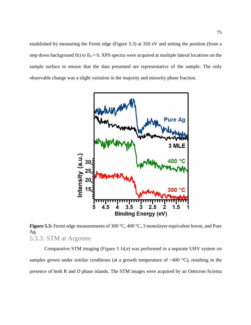
75
established by measuring the Fermi edge (Figure 5.3) at 350 eV and setting the position (from a
step down background fit) to Eb = 0. XPS spectra were acquired at multiple lateral locations on the
sample surface to ensure that the data presented are representative of the sample. The only
observable change was a slight variation in the majority and minority phase fraction.
Figure 5.3: Fermi edge measurements of 300 °C, 400 °C, 3 monolayer-equivalent boron, and Pure
Ag.
5.3.3: STM at Argonne
Comparative STM imaging (Figure 5.1d,e) was performed in a separate UHV system on
samples grown under similar conditions (at a growth temperature of ~400 °C), resulting in the
presence of both R and D phase islands. The STM images were acquired by an Omicron-Scienta

76
Cryo-SPM microscope at 2.5 K in constant-current topography mode, using an electrochemically
etched tungsten tip.
5.4: Synthesis
5.4.1: Synthesis of v1/6 and v1/5 phases
Samples were grown in a dedicated preparation chamber attached to the main X-ray
analysis chamber at beamline I09 at the Diamond Light Source under ultra-high vacuum (UHV, P
< 5 10-10 mbar). Borophene was grown on single-crystal Ag(111) substrates (>99.999% purity)
purchased from Mateck and Surface Preparation Laboratories. Substrates were prepared by
repeating cycles of Ar ion sputtering (1 kV) and annealing (550 °C), and the quality of the surface
was confirmed by LEED and XPS. The Ag(111) substrate was heated radiatively by a ceramic BN
ribbon. The sample temperature was calibrated based on measurements of a reference sample
composed of a diamond substrate bonded to a thermocouple. Boron was deposited from a FOCUS
EFM-3 electron beam evaporator using a solid boron rod (99.9999% purity) purchased from ESPI
metals. The boron deposition rate was monitored with a quartz crystal microbalance (QCM) to
achieve consistent deposition rates of 0.002 Å/s during borophene growth. Boron was deposited
for 20 min to a coverage of nominally 0.3 B/Å2, as defined by the QCM-measured deposition rate
for the 300 °C and 400 °C samples presented in the manuscript. One complete monolayer of
borophene corresponds to 0.35 B/Å2 and 0.29 B/Å2 in the v1/6 and v1/5 models, respectively, as
shown in Figure 5.1b,c. The XSW measurement further constrains the boron coverage, such that
it cannot significantly exceed 1 monolayer. A multilayer boron reference sample was deposited
on Ag(111) at room temperature, yielding a thickness of approximately 8 Å and coverage of 1.06
B/Å2. The relative B 1s intensities being 1.1, 1.0, and 3.9 between the 300 °C and 400 °C
77
borophene and 20 °C multilayer boron samples confirm QCM measurements. Attenuation of the
Ag 3d signal due to the presence of borophene further confirm sub-monolayer overlayers with 0.23
B/Å2 and 0.29 B/Å2 coverage for the 300 °C and 400 °C borophene [172]. LEED patterns were
acquired at room temperature using conventional reverse-view optics (OCI Vacuum
Microengineering).
2D reciprocal space vectors were calculated from the v1/6 and v1/5 structural models
[5,49,101] to provide a comparison for the LEED patterns. LEED patterns were taken at room
temperature using a conventional reverse-view diffractometer (OCI Vacuum Microengineering).
Figure 5.4a,e present simulated reciprocal space vectors a* and b* for the v1/6 and v1/5 models,
respectively. The borophene orientational epitaxy on the 6-fold symmetric Ag(111) surface results
in 3 unique orientations of borophene islands. Because LEED measures over a spot size on the
order of hundreds of microns, all borophene orientations are represented in the LEED patterns.
This effect is replicated by superimposing the calculated reciprocal lattice at 0°, 120°, and 240°
orientations (Figure 5.4b,f).

78
Figure 5.4: Reciprocal space analysis of in-plane borophene atomic structure. (a,e) Calculated
reciprocal lattice for the v1/6 and v1/5 structures, respectively. (b,f) Reciprocal lattices from (a,e),
superimposed for three orientations rotated 120 (green) and 240 (blue), corresponding to the
symmetry observed experimentally over a larger area of the sample. (c,g) FFT of STM images in
Figure 5.1d,e corresponding to the R and D lattices, respectively. (d,h) LEED patterns reproduced
from Figure 5.1g,h for comparison. Note that the LEED determined R lattice in (d) is consistent
with the v1/6 model rotated 30° relative to the Ag lattice in (b).
Additional reciprocal space information can be obtained by calculating the Fourier
transformations of STM images. Figure 5.4c,g shows FFTs calculated for the STM images of the
R phase (Figure 5.1d) and the D phase (Figure 5.1e). In comparison with the calculated reciprocal
space lattices and the FFTs of STM data, we are able to account for the principal features in the
LEED patterns (Figure 5.4d,h). Based on this analysis and literature precedent [6,170], we can
assign the 300 °C as predominantly R phase and the 400 °C as predominantly D phase.
5.4.2: Coverage Calibration
To avoid the modulo-d ambiguity present in the XSW measurement, 0.3 0.1 B/Å2 of
Boron was deposited to maintain sub-monolayer borophene coverage. Where one complete

79
monolayer of borophene corresponds to 0.35 B/Å2 and 0.29 B/Å2 in the v1/6 and v1/5 models,
respectively. The relative B 1s intensities of 1.0, 0.9, and 3.5 between the 300 °C and 400 °C
borophene and 20 °C multilayer boron samples confirm absolute quartz crystal monitor (QCM)
measurements. Absolute coverage was calibrated using a QCM mounted on the backside of the
sample manipulator. Boron flux was measured with the QCM prior to and after deposition onto
the Ag(111) surface. The minimal detectable deposition rate of the QCM is 0.06 Å/s,
approximately 3x higher than the target deposition rate. To achieve a reliable boron flux, QCM
measurements were collected for 10 minutes prior to and after deposition. No clear drift in the
QCM data is present over 30 minutes of collection time. A ~1 mÅ/s discrepancy between the QCM
measurements was found prior to and after boron deposition, which is the primary source of error
in calculated coverage. The SPC-2 manipulator is cooled with water to maintain low pressure
during annealing. The pumping of the water induces cyclical variations in the QCM vibration
readings, therefore all QCM data was taken over an integrated time range over multiple cycles.
Table 5.2: QCM measured B deposition rate prior to and following deposition on Ag(111).
Deposition Rate (mÅ/s) 300 °C 400 °C
QCM Before 2.1 1.6
QCM After 1.1 2.5
Average QCM 1.6±0.5 2.0±0.5
Deposition Time (s) 1,320 1,200
The successful deposition of sub-monolayer borophene was further verified from periodic
LEED measurements during boron deposition. Every 5 minutes, the sample manipulator was
turned away from the B deposition source and put in position for a LEED measurement. The
extension of the LEED system effectively blocked further boron deposition. The series of LEED
80
images clearly shows increasing borophene spot intensity, which confirms the formation of
borophene throughout the 20 minute deposition. The NIST Electron Effective Attenuation Length
Database [152] yielded inelastic mean free path (IMFP) = 5.912 A and transport mean free path
(TMFP) = 5.753 A for 84 eV electrons in boron with θ = 60° and α = 30°.
5.4.3: Borophene Annealing
Post deposition annealing of the 300 °C borophene sample was performed in an attempt to
transition from R to D phase borophene. The sample was brought to 300 °C, the temperature was
then increased at a rate of 25 °C steps every 10 minutes in a step-wise manner. LEED patterns
were taken at every 25 °C step. After reaching 500 °C, the borophene spots were barely visible
above the background from the indirect heating source. Post anneal LEED images (Figure 5.5f)
reveal a considerable reduction in borophene spots intensity for both the majority R and and
minority D phase as compared to the as-grown 300 °C LEED pattern (Figure 5.5a).
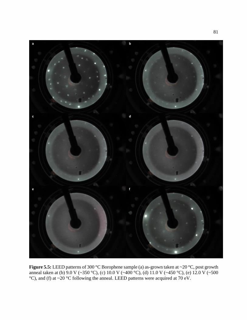
81
Figure 5.5: LEED patterns of 300 °C Borophene sample (a) as-grown taken at ~20 °C, post growth
anneal taken at (b) 9.0 V (~350 °C), (c) 10.0 V (~400 °C), (d) 11.0 V (~450 °C), (e) 12.0 V (~500
°C), and (f) at ~20 °C following the anneal. LEED patterns were acquired at 70 eV.
a b
c d
e f

82
5.5: Results
5.5.1: High-Resolution X-ray Photoelectron Spectroscopy
Figure 5.6: High-resolution XPS of borophene. (a) Boron 1s core-level spectra for borophene
samples grown at 300 °C and 400 °C. (b) Silver 3d core-level spectra of clean Ag(111) and
borophene samples grown at 300 °C and 400 °C. Both plots display the raw data (dots), fitted peak
components (filled shapes), and fitted envelope (grey line).
Figure 5.6 shows high-resolution B 1s and Ag 3d core-level spectra for borophene grown
at 300 °C and 400 °C. In both samples, the B 1s spectra (Figure 5.6a) are composed of a common
set of chemically-shifted components, and are considerably narrower than multilayer boron B 1s

83
spectra (Figure 5.5). This observation suggests that the boron atoms in borophene occupy a number
of discrete local bonding environments. In particular, the spectra can be fit with five individual
components, which we attribute to different B-B coordination numbers present in the two principal
borophene phases: three for the R phase (R4,5,6—i.e, 4-fold, 5-fold, and 6-fold coordination) and
two for the D phase (D4,5—i.e., 4-fold and 5-fold coordination), following the trend observed in
graphene of higher binding energy corresponding to higher coordination [173]. The selective
broadening of the R4,5D4 boron peaks is from distinct vacancy structures at borophene edges and
grain boundaries, which favor low coordination. The relative integrated peak intensity of these
components reflects the proportions of boron atoms in their corresponding chemical environment.
The intensity ratios show the 300 °C sample is ~90% R phase and ~10% D phase, whereas the 400
°C sample is ~10% R phase and ~90% D phase. Moreover, the ratios in peak intensities are
IR4:IR5
:IR6 2:2:1 for the R phase and ID4
:ID5 1:1 for the D phase, which are consistent with the
predicted ratios of 4-fold, 5-fold, and 6-fold coordinated boron atoms in the v1/6 and v1/5 borophene
crystal structures [5,49,101]. In both samples, the Ag 3d spectra (Figure 5.6b) are indistinguishable
from that of clean Ag(111), apart from mild attenuation due to the boron overlayer, which is
indicative of weak B-Ag interactions.
Table 5.3: XPS fitting parameters for Soft and Hard B 1s X-ray spectra taken at identical collection
range of takeoff angle α. Binding energies (Eb) and peak full-width half-maxima (FWHM) are
listed in units of electron Volts. 350 eV Soft X-rays 2.629 keV Hard X-rays
300 °C Borophene 400 °C Borophene 300 °C Borophene 400°C Borophene
B 1s B% Eb FWHM B% Eb FWHM B% Eb FWHM B% Eb FWHM
R4 *36.4 187.3 0.5 †7.0 187.4 0.5 *37.0 187.1 0.8 *6.8 187.0 0.8
R5 *36.4 187.7 0.4 †7.0 187.8 0.4 *37.0 187.5 0.7 *6.8 187.4 0.7
R6 16.0 189.5 0.4 †3.5 189.4 0.3 16.5 189.2 0.6 3.4 189.2 0.6
D4 †5.6 187.6 0.6 40.4 187.6 0.6 *4.5 187.4 0.8 *41.3 187.3 0.7

84
D5 †5.6 188.4 0.3 42.0 188.4 0.3 5.0 188.2 0.5 41.9 188.1 0.6
*,†Values held at fixed relative B% during fitting. Bold indicates majority phase.
The XPS survey data (Error! Reference source not found.) show only boron and silver
core-level peaks, confirming no contamination by carbon, oxygen, or other elemental species. The
survey spectra show binding energies of Ag 3p at 572.7 eV, Ag 3d3/2 at 374.1 eV, Ag 3d5/2 at 368.1
eV, and B 1s at 187.7 eV. Auger MVV peaks were observed at 345 and 351 eV. High-resolution
Ag 3d spectra (Figure 5.6b) are comprised only of Ag 3d3/2 and Ag 3d5/2 spin orbit components.
Figure 5.7: XPS survey, C 1s, and O 1s spectra of borophene 300 °C and 400 °C samples. Survey
scans (left) show binding energies of silver and boron, and no evidence of other elements is
evident, namely, carbon (top-right) or oxygen (bottom-right) from the raw data.
The Ag 3d5/2 Eb of 368.1 eV matches standard binding energies from Ag-Ag metallic bonds (368.2
eV) [174]. High-resolution Ag 3d core-level spectra from a clean Ag(111) control yielded the same
FWHM and Eb as the Ag 3d spectra taken after borophene deposition (Table 5.4), indicating no
major changes to the chemical environment of the surface silver atoms.
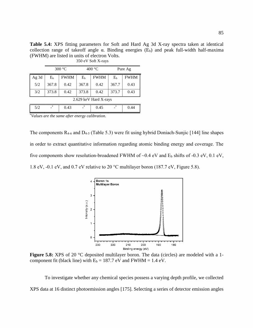
85
Table 5.4: XPS fitting parameters for Soft and Hard Ag 3d X-ray spectra taken at identical
collection range of takeoff angle α. Binding energies (Eb) and peak full-width half-maxima
(FWHM) are listed in units of electron Volts. 350 eV Soft X-rays
300 °C 400 °C Pure Ag
Ag 3d Eb FWHM Eb FWHM Eb FWHM
5/2 367.8 0.42 367.8 0.42 367.7 0.43
3/2 373.8 0.42 373.8 0.42 373.7 0.43
2.629 keV Hard X-rays
5/2 -* 0.43 -* 0.45 -* 0.44
*Values are the same after energy calibration.
The components R4-6 and D4-5 (Table 5.3) were fit using hybrid Doniach-Sunjic [144] line shapes
in order to extract quantitative information regarding atomic binding energy and coverage. The
five components show resolution-broadened FWHM of ~0.4 eV and Eb shifts of -0.3 eV, 0.1 eV,
1.8 eV, -0.1 eV, and 0.7 eV relative to 20 °C multilayer boron (187.7 eV, Figure 5.8).
Figure 5.8: XPS of 20 °C deposited multilayer boron. The data (circles) are modeled with a 1-
component fit (black line) with Eb = 187.7 eV and FWHM = 1.4 eV.
To investigate whether any chemical species possess a varying depth profile, we collected
XPS data at 16 distinct photoemission angles [175]. Selecting a series of detector emission angles
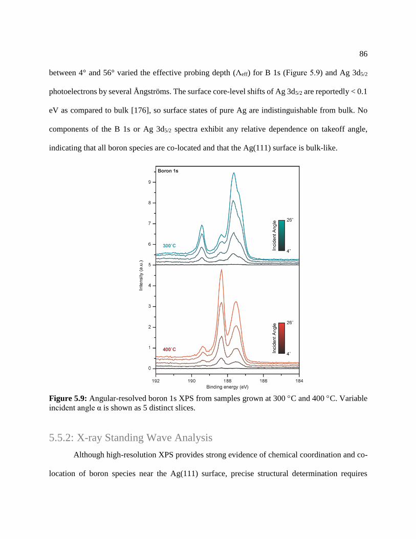
86
between 4° and 56° varied the effective probing depth (Λeff) for B 1s (Figure 5.9) and Ag 3d5/2
photoelectrons by several Ångströms. The surface core-level shifts of Ag 3d5/2 are reportedly < 0.1
eV as compared to bulk [176], so surface states of pure Ag are indistinguishable from bulk. No
components of the B 1s or Ag 3d5/2 spectra exhibit any relative dependence on takeoff angle,
indicating that all boron species are co-located and that the Ag(111) surface is bulk-like.
Figure 5.9: Angular-resolved boron 1s XPS from samples grown at 300 C and 400 C. Variable
incident angle α is shown as 5 distinct slices.
5.5.2: X-ray Standing Wave Analysis
Although high-resolution XPS provides strong evidence of chemical coordination and co-
location of boron species near the Ag(111) surface, precise structural determination requires
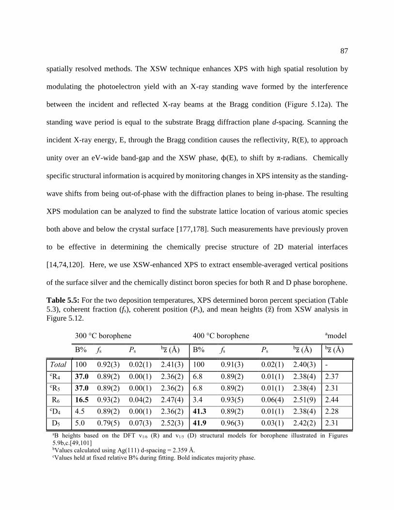
87
spatially resolved methods. The XSW technique enhances XPS with high spatial resolution by
modulating the photoelectron yield with an X-ray standing wave formed by the interference
between the incident and reflected X-ray beams at the Bragg condition (Figure 5.12a). The
standing wave period is equal to the substrate Bragg diffraction plane d-spacing. Scanning the
incident X-ray energy, E, through the Bragg condition causes the reflectivity, R(E), to approach
unity over an eV-wide band-gap and the XSW phase, ϕ(E), to shift by π-radians. Chemically
specific structural information is acquired by monitoring changes in XPS intensity as the standing-
wave shifts from being out-of-phase with the diffraction planes to being in-phase. The resulting
XPS modulation can be analyzed to find the substrate lattice location of various atomic species
both above and below the crystal surface [177,178]. Such measurements have previously proven
to be effective in determining the chemically precise structure of 2D material interfaces
[14,74,120]. Here, we use XSW-enhanced XPS to extract ensemble-averaged vertical positions
of the surface silver and the chemically distinct boron species for both R and D phase borophene.
Table 5.5: For the two deposition temperatures, XPS determined boron percent speciation (Table
5.3), coherent fraction (fs), coherent position (Ps), and mean heights (z̅) from XSW analysis in
Figure 5.12.
300 °C borophene 400 °C borophene amodel
B% fs Ps bz̅ (Å) B% fs Ps bz̅ (Å) bz̅ (Å)
Total 100 0.92(3) 0.02(1) 2.41(3) 100 0.91(3) 0.02(1) 2.40(3) -
cR4 37.0 0.89(2) 0.00(1) 2.36(2) 6.8 0.89(2) 0.01(1) 2.38(4) 2.37 cR5 37.0 0.89(2) 0.00(1) 2.36(2) 6.8 0.89(2) 0.01(1) 2.38(4) 2.31
R6 16.5 0.93(2) 0.04(2) 2.47(4) 3.4 0.93(5) 0.06(4) 2.51(9) 2.44 cD4 4.5 0.89(2) 0.00(1) 2.36(2) 41.3 0.89(2) 0.01(1) 2.38(4) 2.28
D5 5.0 0.79(5) 0.07(3) 2.52(3) 41.9 0.96(3) 0.03(1) 2.42(2) 2.31
aB heights based on the DFT v1/6 (R) and v1/5 (D) structural models for borophene illustrated in Figures
5.9b,c.[49,101] bValues calculated using Ag(111) d-spacing = 2.359 Å. cValues held at fixed relative B% during fitting. Bold indicates majority phase.

88
Depending on the precise atomic distribution the photoelectron yield from a selected
chemical species (s),
𝑌s(𝐸) = 1 + 𝑅(𝐸) + 2√𝑅(𝐸)𝑓s cos(𝜙(𝐸) − 2𝜋𝑃s) , (6. 1)
gives a distinct modulation versus energy that is parameterized by the Fourier amplitude (or
coherent fraction, fs) and phase (or coherent position, Ps) of the distribution profile [122,167].
Roughly speaking the coherent position is a normalized measurement of the atomic average
position z̅s, modulo the 2.359 Å d-spacing of the Ag(111) diffraction plane. The coherent fraction
describes the atomic distribution width normal to the diffraction planes [124]. For example, a
random distribution of atoms would produce fs = 0 and fs = 1 indicates all atoms are precisely
located at Ps.
Figure 5.10: XSW characterization of silver at the borophene/Ag(111) interface. Data (circles)
and eq. 5.1 model fits (black lines) for incident X-ray energy dependence of the X-ray reflectivity
and normalized Ag 3d5/2 photoelectron yields of 400 °C, 300 °C, and pure Ag(111) control samples

89
probed at α = 5.3°. XSW results are identical within error, yielding near-unity coherent fractions
f400°C = 1.08(3), f300°C = 1.03(3), and fpureAg = 1.04(3) and coherent positions P400°C = P300°C = PpureAg
= 0.01(1) with all Ag 3d5/2 photoelectron yields.
The Ag 3d5/2 XSW-XPS yield results in fAg = 1 and PAg = 1 for all samples, indicating that all
silver atoms within the ~10 Å sampling depth are unaffected by the presence of boron.
Figure 5.11: XSW characterization of 20 °C deposited multilayer boron on Ag(111). Data (circles)
and model fits (black lines) for incident X-ray energy dependence of the X-ray reflectivity and
normalized B 1s photoelectron yields of boron. Fits yielded coherent fractions f = 0.22(3) and
coherent positions P = 0.09(1).
In contrast to the nearly random B 1s XSW-XPS distribution (f = ~0.2) for ~3 layers of boron
deposited at 20 °C (Figure 5.11), the total B 1s XPS yield fit of both 300 °C and 400 °C borophene
showed ft > 0.9 and Pt = 0.0 corresponding to a narrow single-layer boron distribution (Gaussian
width σt = 0.15 Å) positioned at 2.4 Å above the topmost Ag(111) atomic planes. Critically, this
measurement indicates that, independent of the specific phase or B-B coordination, all boron atoms
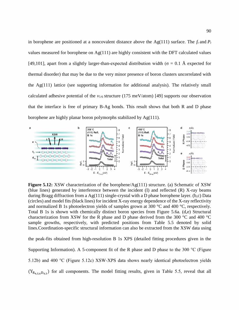
90
in borophene are positioned at a noncovalent distance above the Ag(111) surface. The ft and Pt
values measured for borophene on Ag(111) are highly consistent with the DFT calculated values
[49,101], apart from a slightly larger-than-expected distribution width (σ = 0.1 Å expected for
thermal disorder) that may be due to the very minor presence of boron clusters uncorrelated with
the Ag(111) lattice (see supporting information for additional analysis). The relatively small
calculated adhesive potential of the v1/6 structure (175 meV/atom) [49] supports our observation
that the interface is free of primary B-Ag bonds. This result shows that both R and D phase
borophene are highly planar boron polymorphs stabilized by Ag(111).
Figure 5.12: XSW characterization of the borophene/Ag(111) structure. (a) Schematic of XSW
(blue lines) generated by interference between the incident (I) and reflected (R) X-ray beams
during Bragg diffraction from a Ag(111) single-crystal with a D phase borophene layer. (b,c) Data
(circles) and model fits (black lines) for incident X-ray energy dependence of the X-ray reflectivity
and normalized B 1s photoelectron yields of samples grown at 300 °C and 400 °C, respectively.
Total B 1s is shown with chemically distinct boron species from Figure 5.6a. (d,e) Structural
characterization from XSW for the R phase and D phase derived from the 300 °C and 400 °C
sample growths, respectively, with predicted positions from Table 5.5 denoted by solid
lines.Coordination-specific structural information can also be extracted from the XSW data using
the peak-fits obtained from high-resolution B 1s XPS (detailed fitting procedures given in the
Supporting Information). A 5-component fit of the R phase and D phase to the 300 °C (Figure
5.12b) and 400 °C (Figure 5.12c) XSW-XPS data shows nearly identical photoelectron yields
(YR4,5,6D4,5) for all components. The model fitting results, given in Table 5.5, reveal that all

91
chemically distinct species of borophene are highly planar (f > 0.8) with essentially the same 2.4
Å spacing above the terminal plane of Ag(111) atoms (0.0 < P < 0.1). These results are depicted
schematically in Figure 5.12d,e for the 300 °C and 400 °C borophene samples relative to the v1/6
and v1/5 structures, respectively.
XSW measurements taken at multiple spots across the 300 °C and 400 °C samples were
used to calculate 3σ error bars reported in Table 5.5. Equation 5.1 is derived using the dipole
approximation, quadrapolar effects were taken into account to calculate the coherent fractions and
positions of boron species listed in Table 5.5 [122]. Due to a large degree of spectral overlap, R4,
R5, and D4 peaks were held at constant relative intensity to avoid negative covariance during XSW
fitting. The impact of this constraint on the interpretation of the D4 phase is minimal as the R phase
components are ~10% of the R4+R5+D4 intensity for the 400 °C sample. However, for the 300 °C
sample, this assumption precludes the decoupling of the XSW-induced modulations for the R4 and
R5 signals. Analysis of individual chemical species reveal that the well-isolated 300 °C sample R6
and 400 °C sample D5 signals both exhibit exceptionally high coherent fractions (𝑓R6D5> 0.93)
when compared to the co-constrained R4,5D4 components. It also appears that fs increases for
spectral components with large core-shifts (Table 5.3) relative to the location of the 20 °C
multilayer boron sample peak (187.7 eV). Therefore, one explanation for a relatively low coherent
fraction for low Eb components is the presence of uncorrelated boron. A 5% atomic fraction of
boron with f = 0.2 intermixed (Figure 5.11) with the borophene would be sufficient to reduce the
fs of the R4,5D4 peak from 0.93 to 0.89. Boron clusters scattered across the borophene have
previously been observed in STM, and an atomic fraction near 6% is consistent with large-area
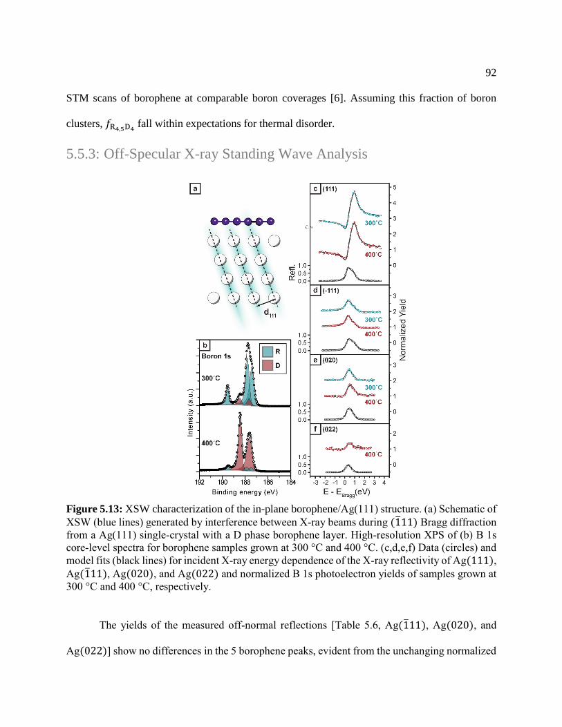
92
STM scans of borophene at comparable boron coverages [6]. Assuming this fraction of boron
clusters, 𝑓R4,5D4 fall within expectations for thermal disorder.
5.5.3: Off-Specular X-ray Standing Wave Analysis
Figure 5.13: XSW characterization of the in-plane borophene/Ag(111) structure. (a) Schematic of
XSW (blue lines) generated by interference between X-ray beams during (1̅11) Bragg diffraction
from a Ag(111) single-crystal with a D phase borophene layer. High-resolution XPS of (b) B 1s
core-level spectra for borophene samples grown at 300 °C and 400 °C. (c,d,e,f) Data (circles) and
model fits (black lines) for incident X-ray energy dependence of the X-ray reflectivity of Ag(111),
Ag(1̅11), Ag(020), and Ag(022) and normalized B 1s photoelectron yields of samples grown at
300 °C and 400 °C, respectively.
The yields of the measured off-normal reflections [Table 5.6, Ag(1̅11), Ag(020), and
Ag(022)] show no differences in the 5 borophene peaks, evident from the unchanging normalized
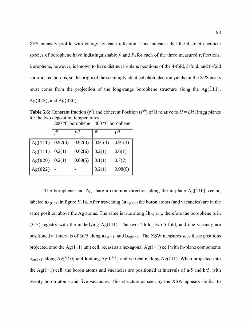
93
XPS intensity profile with energy for each refection. This indicates that the distinct chemical
species of borophene have indistinguishable fs and Ps for each of the three measured reflections.
Borophene, however, is known to have distinct in-plane positions of the 4-fold, 5-fold, and 6-fold
coordinated borons, so the origin of the seemingly identical photoelectron yields for the XPS peaks
must come from the projection of the long-range borophene structure along the Ag(1̅11),
Ag(022), and Ag(020).
Table 5.6: Coherent fraction (fH) and coherent Position (PH) of B relative to H = hkl Bragg planes
for the two deposition temperatures
300 °C borophene 400 °C borophene
fH PH fH PH
Ag(111) 0.92(3) 0.92(3) 0.91(3) 0.91(3)
Ag(1̅11) 0.2(1) 0.62(6) 0.2(1) 0.6(1)
Ag(020) 0.2(1) 0.00(5) 0.1(1) 0.7(2)
Ag(022) - - 0.2(1) 0.98(6)
The borophene and Ag share a common direction along the in-plane Ag[1̅10] vector,
labeled aAg(1×1) in figure 511a. After traversing 3aAg(1×1) the boron atoms (and vacancies) are in the
same position above the Ag atoms. The same is true along 3bAg(1×1), therefore the borophene is in
(3×3) registry with the underlying Ag(111). The two 4-fold, two 5-fold, and one vacancy are
positioned at intervals of 3n/5 along aAg(1×1) and bAg(1×1). The XSW measures sees these positions
projected onto the Ag(111) unit cell, recast as a hexagonal Ag(1×1) cell with in-plane components
aAg(1×1) along Ag[1̅10] and b along Ag[01̅1] and vertical c along Ag(111). When projected into
the Ag(1×1) cell, the boron atoms and vacancies are positioned at intervals of a/5 and b/5, with
twenty boron atoms and five vacancies. This structure as seen by the XSW appears similar to
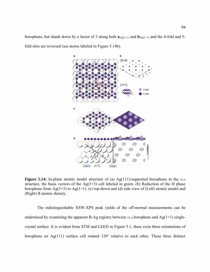
94
borophene, but shank down by a factor of 3 along both aAg(1×1) and bAg(1×1) and the 4-fold and 5-
fold sites are reversed (see atoms labeled in Figure 5.14b).
Figure 5.14: In-plane atomic model structure of (a) Ag(111)-supported borophene in the v1/5
structure, the basis vectors of the Ag(3×3) cell labeled in green. (b) Reduction of the D phase
borophene from Ag(3×3) to Ag(1×1). (c) top-down and (d) side view of (Left) atomic model and
(Right) B atomic density.
The indistinguishable XSW-XPS peak yields of the off-normal measurements can be
understood by examining the apparent B-Ag registry between v1/5 borophene and Ag(1×1) single-
crystal surface. It is evident from STM and LEED in Figure 5.1, there exist three orientations of
borophene on Ag(111) surface cell rotated 120° relative to each other. These three distinct
95
borophene domains are attributed to the p6m symmetry of the underlying Ag(111) which is
imposed on the borophene, which has cmm (or less) symmetry. The XSW measures these three
domains simultaneously, which once averaged, have equal fractions of 4-fold and 5-fold boron at
a given position when projected onto the Ag(1̅11), Ag(022), and Ag(020) lattice planes.
Despite the 20 boron atoms with at least 5 distinct positions relative to the Ag(1×1),
measured coherent fractions in Table 5.6 were as much as 0.2 for the off-normal reflections.
Critically, this indicates definite long-range commensuration between the borophene and Ag(111)
substrate (fH = 0 for incommensurate structures), with boron atoms located periodically above
particular Ag(111) sites. A Fourier inversion method was used to determine the averaged structure
of borophene within the Ag(1×1) [133]. Each measured XSW reflection provides a Fourier
component of the 3D atomic density of boron. The summation of orthogonal set of hkl Fourier
components with fH and PH generates a model-independent 3D map ρ(r), shown in Figure 5.14c,d
for B 1s and Ag 3d5/2.
𝑓𝐻𝑒2π𝑖𝑃𝐻= ∫ 𝜌(𝐫) 𝑒−𝑖𝐆𝐻∙𝐫d𝐫 (6. 2)
For the case of the Ag 3d5/2 yield, the sum of the measured Fourier components gives an atomic
density map with the familiar FCC structure, with resolution given by the measured coherent
components. The Fourier inversion of the B 1s yields reveals the atomic structure of borophene is
highly planar, but with some non-uniformities in the concentration of boron atoms. The areas of
highest boron concentration are located directly above the terminating Ag(111) atoms, which
indicates that boron atoms prefer to be close to the Ag atoms. However, relating these features to
boron atoms proves challenging, because the spacing of Fourier components is much greater than
96
the projected distance between boron atoms. Model-depending fitting analysis is underway to help
resolve this structure.
5.6: Conclusions
Based on the boron 2D lattice determination by LEED, the coordination by XPS, and height
by XSW, the R and D phases observed in STM [5,6] are confirmed to be distinct in-plane vacancy
configurations as predicted computationally for the v1/6 and v1/5 phases [5,49,101]. This conclusion
implies that borophene exhibits a unique 2D, vacancy-mediated form of structural degeneracy that
is reminiscent of the complexity observed in 3D boron allotropes. This polymorphism within the
borophene family further suggests that the properties of borophene and its derivatives can be
systematically modified based on substrate interactions, strain, and other parameters. Overall,
these results demonstrate that materials without layered bulk allotropes can be induced to form
highly planar structures at the 2D limit based purely on non-covalent interactions with metal
substrates, thereby establishing a new class of synthetic 2D materials.

97
Chapter 6: EG/Ge(110) Reconstruction
Understanding and engineering the properties of crystalline surfaces has been critical in
achieving functional electronics at the nanoscale. Employing scanning tunneling microscopy,
surface X-ray diffraction, and high-resolution X-ray reflectivity experiments, we present a
thorough study of epitaxial graphene (EG)/Ge(110) and report a Ge(110) “6×2” reconstruction
stabilized by the presence of epitaxial graphene unseen in group-IV semiconductor surfaces. X-
ray studies reveal that graphene resides atop the surface reconstruction with a 0.34 nm van der
Waals (vdW) gap and provides protection from ambient degradation.
6.1: Introduction
Single-crystal group-IV semiconductor surfaces, as a termination of ideal bulk crystals,
draw significant interest for their tendency toward complex and highly anisotropic atomic orbital
relaxations [179-185] accompanied by the emergence of energetically distinct surface states
[186,187]. Effective surface passivation of group-IV semiconductors ultimately enables
neutralization of the unbound orbitals at semiconducting surfaces [188-190], a crucial
advancement in large-scale microelectronics fabrication. Most studies, however, have focused
exclusively on intrinsic reconstructed surfaces or engineered reconstructions via reactive
chemistry. In contrast, the ability to influence chemically homogeneous semiconductor interfaces
via van der Waals interactions has not yet been explored.
Graphene synthesized on single-crystal surfaces produces a confined 2D space which
stimulates the intercalation of impurity atoms [191,192] and the formation of new 2D materials
[4]. This confined interface accommodates a new perspective on semiconductor surface
reconstructions by the recent chemical vapor deposition (CVD) synthesis of van der Waals (vdW)

98
epitaxial graphene (EG) atop atomically flat Ge(110) wafers [81,193]. The chemically inert sp2-
bonded lattice of graphene [30], protects the Ge surface from ambient while allowing diffusion of
atomic species at the encapsulated surface [84,194]. The Ge atoms rearrange into a disordered
phase at the ~900 °C synthesis temperature, with no evident long-range periodicity [83]. Despite
apparently weak vdW bonding, our earlier work [82] showed that interactions at EG/Ge(110)
interface led to induced strain and doping of the graphene accompanied by changes in the physical
structure of the Ge surface layer. Scanning tunneling microscopy (STM) studies of the annealed
EG/Ge(110) interface showed a graphene lattice on top of what appeared to be an ordered 1D
reconstruction of the Ge surface atoms with a 2 nm period [82] along the 112
direction. These
striped features are also observed in the pristine Ge(110) “16x2” reconstruction, however with a
much larger 5 nm period [183-185,195-198], making this EG stabilized Ge structure distinct from
those previously reported.
Figure 6.1: STM images of graphene on Ge(110) showing (a) perspective view (size: 500 nm ×
310 nm, V = 2 V, I = 100 pA), (b) graphene honeycomb lattice atop of as-grown Ge(110) terrace
(scale bar = 2 nm, V = 1.4 V, I = 80 pA). Inset: Fourier transform of (b) with 6-fold symmetry of
graphene indicated by dotted hexagon (scale bar = 2 nm–1), (c) graphene honeycomb lattice atop
annealed 2D reconstruction of the Ge(110) (scale bar = 2 nm, V = −1 V, I = 400 pA). (Source:
adapted from Ref. [82])

99
Herein, we report a more detailed, higher spatial resolution structural description of this
interface by combining grazing incidence X-ray diffraction (GIXD) and high-resolution X-ray
reflectivity (XRR) measurements with STM. These highly surface sensitive atomic-scale
measurements reveal relaxation of the top-most Ge layers and document the emergence of a
surface reconstruction specific to EG/Ge(110). In this particular system, the robust orbital structure
of graphene enables the study of vdW interactions at the EG/Ge(110) surface at temperatures
approaching the Ge melting point. Upon annealing the EG/Ge(110) surface in ultra-high vacuum
(UHV), we show that the presence of the EG introduces a perturbation to the crystalline surface
causing it to adopt a specific, long-range order with a Ge(110) “6×2” unit cell, previously
unobserved on any group-IV semiconducting surface. Local and global measurements confirm a
novel surface 2D reconstruction based on the rearrangement of Ge atoms in the topmost layers of
the bulk crystal. Examining the EG/Ge(110) interface with sub-Å resolution verifies a vdW gap
between graphene and a partially filled Ge buffer layer. Thus, encapsulation of the Ge(110) surface
with EG enables the emergence of an air-stable, ordered Ge surface reconstruction covering nearly
the entire Ge(110) surface.
6.2: Methods
6.2.1: Sample Preparation
Ge(110) wafers (University Wafer, resistivity 0.1-0.5 Ω-cm with Ga or Sb dopants) were
placed into a horizontal quartz tube furnace (inner diameter of 34 mm) and the system was
evacuated to ~10-6 Torr. The chamber was then filled to atmospheric pressure with 200 sccm of
Ar (99.999 %) and 100 sccm of H2 (99.999 %). The Ge samples were annealed at 910 °C for 30
minutes, after which 3.6-4.6 sccm of CH4 (99.99 %) was introduced for graphene synthesis. To

100
terminate growth, samples were rapidly cooled in the same atmosphere used during synthesis by
sliding the furnace away from the growth region.
The as-grown graphene on Ge(110) samples were transferred ex-situ into UHV (<10-10
mbar) and degassed for 1-2 hrs at ~400 °C. Annealed samples were heated to ~700 °C in UHV for
1-2 hrs. The graphene physical and electronic structure were characterized with STM in an
Omicron VT with a base pressure of 10-11 mbar. STM measurements were performed on both
samples at room temperature using electrochemically etched W tips.
6.2.2: X-ray photoelectron spectroscopy
XPS data were collected ex situ using a Thermo Scientific ESCALAB 250X in the KECK
II facility at Northwestern University. The ESCALAB is equipped with a monochromatic Al Kα
X-ray source incident at 45° with a 650 μm spot size. Photoelectrons were collected in a
hemispherical energy analyzer with a 15 eV pass energy and 0.1 eV step size. A low-energy
electron flood gun was used to compensate for charge accumulation on the sample surface. The
Fermi energy was used to calibrate the XPS energy.
6.2.3: Synchrotron X-ray Measurements
High-resolution X-ray measurements were performed at the Advanced Photon Source
(APS) station 33ID-D of Argonne National Laboratory. Out-of-plane XRR and in-plane GIXD
data were collected for an as-grown EG/Ge(110) sample and then for that same sample after
annealing it to 700 °C. Monochromatic 10.00 keV (wavelength λ = 0.1240 nm) X-rays were
focused to 70 μm × 30 μm using a Kirkpatrick-Baez mirror with a flux of 2×10¹¹ photons/s. To
reduce oxidation, the sample was kept in a He/H atmosphere. Data were collected using a Dectris
100K Pilatus area detector mounted on a Newport 6-circle goniometer. The XRR and GIXD
101
intensities from the area detector were extracted following established experimental methods
provided in Refs. [137,199].
Uncertainties in the extracted XRR and GIXD intensities were computed based on counting
statistics, while enforcing 2% and 8% minimum error bars during fitting of the XRR and GIXD
data, respectively. The XRR data were fit between Qz = 8.4 to 44.0 nm-1 using model-based
analysis. The measurement range is reported in the out-of-plane component (Qz) of the momentum
transfer vector Q = 4π Sin(2θ/2)/λ , where the scattering angle 2θ is defined as the angle between
the incident and scattered wavevectors ki and kf , respectively.
GIXD data were collected at fixed α = β = 0.2° geometry between Qxy = 3.5 to 44.0 nm-1;
where α and β are the angles between the surface and wavevectors ki and kf , respectively. The
critical angle for total external reflection of 10.00 keV X-rays from an ideal Ge mirror is αc =
0.245°; in which case the critical scattering vector Qc = 0.433 nm-1. Based on the evanescent wave
effect for the refraction of the incoming and outgoing X-rays, [200] the scattered X-rays are
probing an effective depth of 2.0 nm, i.e., the 10th Ge layer contributes e-1 times the top Ge layer
[109,200]. All in-plane, allowed and forbidden, bulk Ge reflections were ignored in GIXD
analysis. In total, 158 reflections were measured to optimize the in-plane structure using integrated
intensity azimuthal φ scans. Of the 158 reflections measured, 134 were unique based on symmetry.
GIXD integrated peak intensities were background subtracted and corrected for the Lorentz
polarization factor following standard convention [199].

102
6.3: Results
Figure 6.2: STM data of annealed EG/Ge(110) (V = -1 V, I = 400 pA) with enhanced sensitivity
to underlying Ge(110) atomic planes. Left inset: the (01) planes (red) of the unreconstructed
Ge(110)-(1x1) phase. Right inset: proposed Ge(110) reconstructed unit cell (red). The
superstructure cell is defined with reciprocal space STM data that show lattice points
corresponding to (b) the orientation and spacing of *
1x1b and (c) the Ge(110) “6×2”
superstructure with lattice parameters *
sa = 3.1 nm-1, *
sb = 5.0 nm-1, and ɣ = 120°. (STM
image provided by B.T. Kiarly)
Upon annealing EG/Ge(110) samples to 700 °C under ultra-high vacuum (UHV)
conditions, STM images show the formation of an in-plane reorganization of the underlying
Ge(110) surface Figure 6.2a,right. In some regions of the samples, the Ge(110) reconstruction can
be seen alongside a metastable, unreconstructed Ge(110)-(1x1) phase Figure 6.2a,left. Close
examination of the fast Fourier transform of the Ge(110)-(1x1) surface Figure 6.2b confirms a
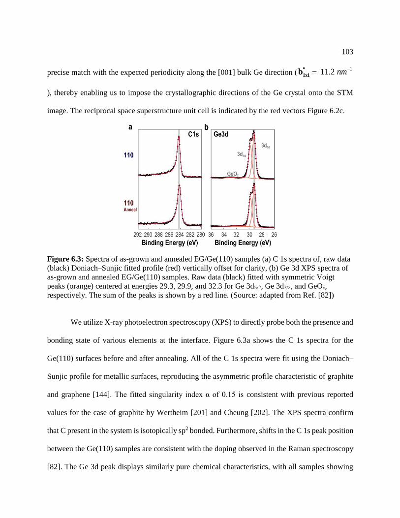
103
precise match with the expected periodicity along the [001] bulk Ge direction (1 11.2 nm*
1x1b
), thereby enabling us to impose the crystallographic directions of the Ge crystal onto the STM
image. The reciprocal space superstructure unit cell is indicated by the red vectors Figure 6.2c.
Figure 6.3: Spectra of as-grown and annealed EG/Ge(110) samples (a) C 1s spectra of, raw data
(black) Doniach–Sunjic fitted profile (red) vertically offset for clarity, (b) Ge 3d XPS spectra of
as-grown and annealed EG/Ge(110) samples. Raw data (black) fitted with symmetric Voigt
peaks (orange) centered at energies 29.3, 29.9, and 32.3 for Ge 3d5/2, Ge 3d3/2, and GeOx,
respectively. The sum of the peaks is shown by a red line. (Source: adapted from Ref. [82])
We utilize X-ray photoelectron spectroscopy (XPS) to directly probe both the presence and
bonding state of various elements at the interface. Figure 6.3a shows the C 1s spectra for the
Ge(110) surfaces before and after annealing. All of the C 1s spectra were fit using the Doniach–
Sunjic profile for metallic surfaces, reproducing the asymmetric profile characteristic of graphite
and graphene [144]. The fitted singularity index α of 0.15 is consistent with previous reported
values for the case of graphite by Wertheim [201] and Cheung [202]. The XPS spectra confirm
that C present in the system is isotopically sp2 bonded. Furthermore, shifts in the C 1s peak position
between the Ge(110) samples are consistent with the doping observed in the Raman spectroscopy
[82]. The Ge 3d peak displays similarly pure chemical characteristics, with all samples showing

104
the characteristic 3d5/2 and 3d3/2 doublet of elemental germanium. A minor GeOx peak is present
in the Ge(111) samples, pointing to a minor degree of surface oxidation likely due to the presence
of grain boundaries in the graphene. Significantly, all spectra show an absence of Ge–C bonds,
confirming the chemical integrity of the graphene before and after annealing.
Table 6.1: Results of model dependent fit to XRR data listing vertical height (Ζ), layer occupancy
fraction (Θ), and distribution width (σ) fitting parameters for as-grown and annealed “6×2”
Ge(110). Z is vertical displacement relative to the top-most Ge(110) bulk-like atomic plane, Θ is
in units of bulk-like 2D atomic densities (8.8 nm-2 for Ge(110) planes and 38.2 nm-2 for EG).
Uncertainty of 3 standard deviations is given in parentheses.
As-Grown EG/Ge(110) Annealed EG/Ge(110) “6×2”
Layer Ζ (nm) Θ σ (nm) Ζ (nm) Θ σ (nm)
Ge1 0.201(2) 0.98(3) 0.0068(6) 0.201(2) 0.99(3) 0.0075(4)
Ge2 0.404(2) 0.95(6) 0.008(1) 0.402(2) 0.93(8) 0.008(1)
Ge3 0.601(1) 0.87(8) 0.017(5) 0.600(2) 0.9(2) 0.017(7)
Ge4 Bulk 0.81(1) 0.8(2) 0.02(1) 0.80(2) 0.6(3) 0.01(2)
Buckled 0.85(8) 0.1(1) †0.022 0.85(4) 0.2(2) †0.025
Ge5 Buffer 0.96(2) 0.6(1) 0.043(3) 0.96(2) 0.7(1) 0.03(2)
EG1 1.30(1) 0.9(1) 0.024(4) 1.30(1) 0.9(1) 0.021(9)
EG2 1.64(1) 0.4(1) 0.029(9) 1.64(3) 0.4(1) †0.036
†Fixed parameter value.
The electron density profile along the [110] direction for the EG/Ge(110) interface was
determined from a model-dependent fit to the specular reflectivity data Figure 6.4. The XRR data
(Figure 6.4a) show orders-of-magnitude changes in scattered intensity as compared to the ideal
bulk terminated surface, indicating distinct positions for the surface Ge and overlaying graphene.
The peaks at 32 nm-1 and 64 nm-1 are consistent with Bragg scattering from single-crystal Ge(220)
and Ge(440) planes with characteristic 0.200 nm atomic plane spacing. The most notable
deviations from the XRR of the ideal Ge(110) bulk crystal (Figure 6.4a) are the peaks near Qz =
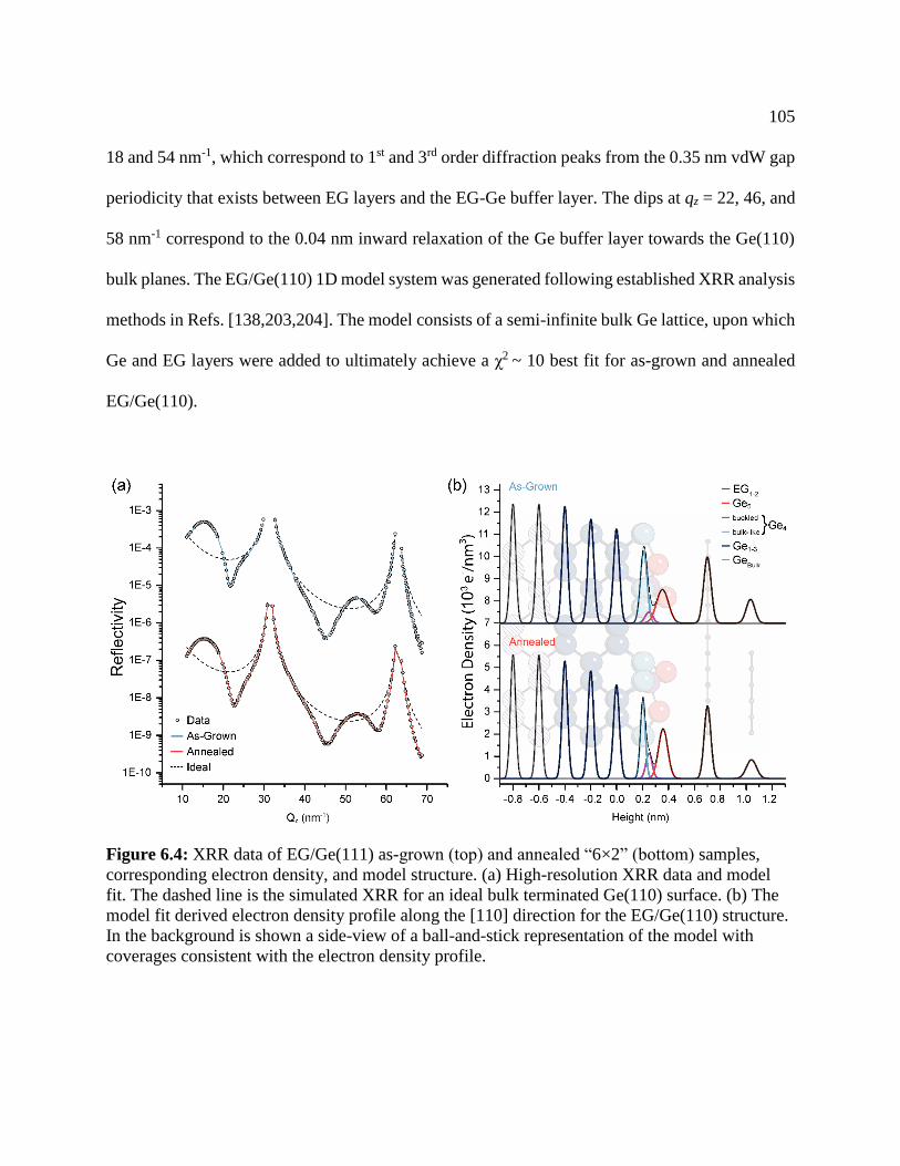
105
18 and 54 nm-1, which correspond to 1st and 3rd order diffraction peaks from the 0.35 nm vdW gap
periodicity that exists between EG layers and the EG-Ge buffer layer. The dips at qz = 22, 46, and
58 nm-1 correspond to the 0.04 nm inward relaxation of the Ge buffer layer towards the Ge(110)
bulk planes. The EG/Ge(110) 1D model system was generated following established XRR analysis
methods in Refs. [138,203,204]. The model consists of a semi-infinite bulk Ge lattice, upon which
Ge and EG layers were added to ultimately achieve a χ2 ~ 10 best fit for as-grown and annealed
EG/Ge(110).
Figure 6.4: XRR data of EG/Ge(111) as-grown (top) and annealed “6×2” (bottom) samples,
corresponding electron density, and model structure. (a) High-resolution XRR data and model
fit. The dashed line is the simulated XRR for an ideal bulk terminated Ge(110) surface. (b) The
model fit derived electron density profile along the [110] direction for the EG/Ge(110) structure.
In the background is shown a side-view of a ball-and-stick representation of the model with
coverages consistent with the electron density profile.

106
The model fit (Figure 6.4b) of the Ge(110) interface is constructed from 5 Ge layers with
6 distinct vertical Ge atomic positions and an EG layer with a partial EG bilayer. The best-fit
positions (Ζ), occupancies (Θ), and distribution widths (σ) of the EG/Ge(110) for both the as-
grown and “6×2” reconstructed XRR data are enumerated with 3 sigma confidence in Table 6.1.
The first three layers of Ge (Ge1-3) atop the semi-infinite Ge crystal remain at bulk positions (0.200
nm), but with a gradual increase in vacancy concentrations and distribution width broadening
compared to bulk Ge. The fourth layer (Ge4) and fifth layer (Ge5) of Ge deviate substantially from
bulk, forming a relaxed Ge complex consisting of a partially buckled layer underneath an inward
relaxed surface layer, which relaxes further upon annealing. For the fourth layer of the as-grown
interface, 80 ± 20% of the Ge atoms sit at the height of bulk Ge(110) planes, with the remaining
10% buckled outward 0.04 ± 0.08 nm towards the EG. The inclusion of a buckled subsurface layer
has been used previously in simulated pristine uncovered Ge(110) reconstructions and helps to
stabilize the topmost Ge buffer layer (Ge5) [183,184]. A 60 ± 10% occupancy Ge buffer layer
(Ge5) is relaxed 0.05 ± 0.01 nm inward from its bulk position. The nearly 50% vacancy
concentration in Ge5 allows in-plane diffusion of the Ge, enabling the reorganization of the surface
into the “6x2” superstructure upon annealing to 700 °C under UHV conditions. The annealed
“6x2” EG/Ge(110) shows a sharpening of the interface (~0.01 nm) accompanied by diffusion of
Ge into the reconstructed buckled and surface layers. When compared to other models for
uncovered Ge(110) surface reconstructions [183,184,196,197], the model Ge(110) vertical
structure shares key commonalities, namely broadening of the bulk Ge(110) layers, a buckled
surface layer, and a partially occupied topmost layer shifted from its ideal position toward the
Ge(110) bulk.
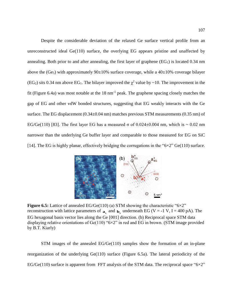
107
Despite the considerable deviation of the relaxed Ge surface vertical profile from an
unreconstructed ideal Ge(110) surface, the overlying EG appears pristine and unaffected by
annealing. Both prior to and after annealing, the first layer of graphene (EG1) is located 0.34 nm
above the (Ge5) with approximately 90±10% surface coverage, while a 40±10% coverage bilayer
(EG2) sits 0.34 nm above EG1. The bilayer improved the χ2 value by ~10. The improvement in the
fit (Figure 6.4a) was most notable at the 18 nm-1 peak. The graphene spacing closely matches the
gap of EG and other vdW bonded structures, suggesting that EG weakly interacts with the Ge
surface. The EG displacement (0.34±0.04 nm) matches previous STM measurements (0.35 nm) of
EG/Ge(110) [83]. The first layer EG has a measured σ of 0.024±0.004 nm, which is ~ 0.02 nm
narrower than the underlying Ge buffer layer and comparable to those measured for EG on SiC
[14]. The EG is highly planar, effectively bridging the corrugations in the “6×2” Ge(110) surface.
Figure 6.5: Lattice of annealed EG/Ge(110) (a) STM showing the characteristic “6×2”
reconstruction with lattice parameters of sa and
sb underneath EG (V = -1 V, I = 400 pA). The
EG hexagonal basis vector lies along the Ge [001] direction. (b) Reciprocal space STM data
displaying relative orientations of Ge(110) “6×2” in red and EG in brown. (STM image provided
by B.T. Kiarly)
STM images of the annealed EG/Ge(110) samples show the formation of an in-plane
reorganization of the underlying Ge(110) surface (Figure 6.5a). The lateral periodicity of the
EG/Ge(110) surface is apparent from FFT analysis of the STM data. The reciprocal space “6×2”

108
unit cell is indicated by the red vectors alongside the epitaxial graphene (Figure 6.5b). To study
the Ge(110) “6×2” atomic rearrangement over large-areas and with enhanced Ge sensitivity, GIXD
was performed on both the as-grown and annealed EG/Ge(110). GIXD maxima of the as-grown
EG/Ge(110) match expected Bragg peaks from the Ge(110) bulk crystal. The annealed
EG/Ge(110) GIXD data show additional in-plane diffraction maxima. These maxima (Figure 6.6a)
appear at 2D superstructure reciprocal lattice points hsks defined by basis vectors 1
6*
s 111a G and
1
12*
s 115b G , where Ghkl are reciprocal lattice vectors for diamond-cubic bulk Ge with lattice
constant 0.5658 nm. The real space “6×2” unit cell basis vectors as and bs have lengths 2.08 nm
and 1.39 nm along the 552
and 112
directions, respectively, with angle ɣ = 70.5°. The
transformation matrix
2 21
12 1 5
**
s1x1
**
s1x1
aa
bb (6. 1)
relates the reciprocal lattice basis vectors of the 2D superstructure to the (1x1) basis vectors of the
Ge (110) bulk-terminated surface. In real space, the superstructure can be properly referred to in
matrix notation as 5 1
2 2
or in Wood notation as Ge(110) “6×2”, being a non-rectangular
superstructure of the rectangular Ge(110)-(1x1) basis with 552
1
2dsa and
112dsb .

109
Figure 6.6: GIXD surface characterization of EG/Ge(110). (a) GIXD measured values of 2
S Sh kF in 2D reciprocal space indexed in hs and ks of the Ge(110) “6×2” basis. The measured
values are proportional to the areas of the hollow circles. The statistical error (red) is indicated
by the perimeter width of each circle. Bulk Ge(110) reflections are marked with an x (blue). (b)
The contour map of the direct space Patterson function for the Ge(110) “6×2” surface from eq.
6.2. All peaks with values greater than ¼ the origin peak are shown.
The areas of the hollow black circles in Fig. 3(a) are proportional to the values of 2
S Sh kF ,
which are derived from the measured in-plane (Qz = 0) integrated scattered intensities at each Ge
2D superstructure peak. S Sh kF is the 2D structure factor [109], which is sensitive to the atomic
arrangement of the Ge atoms within the “6×2” unit cell. Directly extracting Ge positions through
the complex Fourier inversion of S Sh kF is not possible due to the missing phase of
S Sh kF . Instead,
we use a Fourier inversion of the set of 134 symmetry inequivalent 2
S Sh kF values that leads to a
model-independent 2D map of displacement vectors between Ge atoms in the “6x2” reconstructed
surface. This 2D Patterson method is a viable first step in solving surface structures with several
110
symmetry-inequivalent atomic sites from GIXRD data as previously demonstrated [132,205,206].
The 2D electron density correlation function
2
,
1, cos 2
S S
s s
h k s s
h k
P x y F h x k yA
(6.2)
was used to generate the measured 2D Patterson map in Fig. 3(b), where x and y are the fractional
coordinates of the unit cell with area A. The peak at the origin is the sum of the self-correlation of
all displaced Ge atoms at the surface. The surround peaks represent vector displacements between
atoms on the surface. By applying graph theory, the ~11 symmetry inequivalent non-origin strong
peaks (max value > 0.3 Pmax) come from a minimum of 4 or 5 distinct high-density regions (i.e.
clusters of Ge atoms) for a non-centrosymmetric or centrosymmetric unit cell, respectively. The
ratios of Patterson peak values between these strong peaks and the peak at the center of the unit
cell is proportional to the overall number of Ge atoms with this displacement. The XRR derived
model [Fig. 1(b)] shows that the topmost Ge layer is comprised of 16 ± 2 Ge within the “6x2” unit
cell compared to 24 atoms in the same area within a bulk-like (110) Ge layer. The strongest non-
origin peaks in the Patterson map show ~¼ the value of the center peak, indicating that these Ge
displacements are experienced by ~4 Ge in the “6x2” surface unit cell. The high concentration of
peaks along the s sa b direction suggests the formation of ordered Ge clusters underneath the
graphene displaced relative to each other along s sa b [shown by a dashed line in Figure 6.6b.
A similar feature can be seen in STM (Figure 6.2a) and matches observations of pentagon-like
rings in the well-studied “16×2” reconstruction of pristine Ge(110) and Si(110) in UHV
[183,184,195,196,207-209]. The prominent peaks along the bs or 112
direction match the
periodic corrugated ribbons seen in the STM of graphene atop the EG/Ge(110) “6×2”

111
reconstruction (Figure 6.5a). Here we are resolving displacements between individual clusters of
Ge atoms. To resolve the individual atomic positions would require a much larger set of GIXD
peaks or a GIXD – theory combined approach.
6.4: Conclusions
In summary, we used STM, GIXD, and XRR data to reveal the formation of a previously
unidentified Ge(110) “6×2” reconstruction upon annealing, stabilized by weak vdW interactions
of EG 0.34±0.04 nm atop a reordered Ge(110) surface. Through model-independent analysis of
GIXD and STM, we show that annealing EG/Ge(110) leads to a reorganization of the Ge buffer
layer into Ge clusters positioned along the 112
bulk Ge direction. XRR reveals a vertical
relaxation of a Ge surface and verifies the integrity of the vdW gap between the Ge and overlaying
graphene after the formation of the Ge(110) “6×2” reconstruction. The graphene atop the Ge
further acts as an encapsulating layer, protecting the Ge(110) surface in ambient. This non-
destructive approach for controlling atomic surface reconstructions with vdW materials represents
a methodology for engineering single-crystal surfaces and interfaces.

112
Chapter 7: EG/SiC(0001) Heterostructures
Atomically thin MoS2/graphene heterostructures are promising candidates for
nanoelectronic and optoelectronic technologies. When synthesized on epitaxial graphene (EG) on
SiC, these heterostructures exhibit high electronic quality and wafer-scale processability owing to
commensurate growth enabled by van der Waals epitaxy. We examine here the thickness-
controlled van der Waals epitaxial growth of MoS2 on EG via chemical vapor deposition, giving
rise to transfer-free synthesis of a two-dimensional heterostructure with registry between its
constituent materials. The rotational commensurability observed between the MoS2 and EG is
driven by the energetically favorable alignment of their respective lattices and results in nearly
strain-free MoS2, as evidenced by synchrotron X-ray scattering.
7.1: Introduction
Vertical heterostructures composed of stacked two-dimensional (2D) materials allow the
exploration of fundamental interfacial interactions and novel electronic functionality. The
MoS2/graphene heterostructure [107,210] is a model 2D metal/semiconductor heterostructure
which uses the full potential of both materials due to complementary carrier mobilities and optical
responsivities [211]. The properties of MoS2/graphene heterostructures depend strongly on the
underlying substrate and the graphene synthesis technique. Controlling rotational alignment on a
large-scale ensures 2D materials will have reproducible properties on a wafer-scale. Epitaxial
graphene (EG) grown on SiC by the preferential thermal desorption [92,212,213] produces
uniform large-area synthesis of graphene unperturbed by the underlying substrate, particularly
after the decoupling of the buffer layer by post-annealing in hydrogen [191,214]. Furthermore, the
113
functionality of these heterostructures could be tailored though atomic intercalation of the EG/SiC
buffer layer [215-217].
The atomic-scale electronic and structural properties of MoS2/EG heterostructures have not
been thoroughly established. Towards these ends, we report here the rotationally commensurate
growth of atomically thin MoS2 crystals on EG by van der Waals epitaxy. We investigate the
electronic and structural properties of the resulting MoS2/EG heterostructures with synchrotron X-
ray reflectivity (XRR) and grazing incidence X-ray scattering (GIXS) as part of a comprehensive
suite of methods including atomic force microscopy (AFM), ultra-high vacuum (UHV) scanning
tunneling microscopy and spectroscopy (STM/STS), in situ X-ray photoelectron spectroscopy
(XPS), and Raman spectroscopy, which are discussed further in our collaborative work [106].
These X-ray techniques are then extended to mixed dimensional vdW heterostructures, which
integrate graphene with 0D fullerenes [32], 1D nanotubes[218], and 3D crystals [23] to form
mixed-dimensional vdW heterostructures [219].
7.2: Methods
7.2.1: Synthesis of MoS2
High-quality EG was grown on a 9 mm × 5 mm n-type 4H-SiC(0001) wafer (Cree Inc.). The
wafer was sonicated successively in acetone and isopropyl alcohol (IPA) for 10 minutes each.
Subsequently, the substrates were transferred to an ultra-high vacuum (UHV) chamber (∼5 × 10⁻¹⁰
Torr) where they were degassed at 550 °C for ~12h. EG was grown on the Si face of the wafer by
direct heating and thermal desorption of Si atoms at 1270 °C for 20 minutes (with temperature
ramping rate of 100 °C/min and cooling rate of 50 °C/min).
114
To produce MoS2 on EG, Molybdenum trioxide (MoO3, 99.98% trace metal Sigma Aldrich)
was placed in the middle of the hot zone of a Lindberg/Blue 1’’ quartz tube furnace in an alumina
boat 2.5 cm upstream of a 5 mm × 9 mm EG substrate (graphitized Si face is facing up). The sulfur
powder (Sigma Aldrich) in an alumina boat was placed 30 cm upstream of the MoO3 boat under a
PID temperature controlled heating belt. The tube was initially pumped to a base pressure of ~50
mTorr and purged with Ar gas to 400 Torr. During the anneal prior to the reaction and during the
reaction itself, the pressure was kept constant at 43 Torr (to yield mostly monolayer MoS2 crystals)
using a needle valve controller and Ar carrier gas flowing at 25 sccm. The MoO3 and EG substrate
were annealed for 20 min at 150 °C (with a 5 min ramp to 150 °C from room temperature) to
eliminate residual water and physisorbed contaminants in the tube and on the substrate.
Subsequently, the furnace was heated to a maximum temperature of 800 °C at a rate of 12 °C/min.
Once the target temperature was reached, the furnace was kept at 800 °C for 20 min and cooled
down naturally to room temperature. Concurrently, the sulfur was annealed under the same inert
conditions for 49 min at 50 °C (with 5 min ramp to 50 °C from room temperature) and brought to
a maximum temperature of 140 °C at a rate of 4 °C/min. The sulfur ramp to 140 °C began when
the furnace was approximately at 500 °C. The sulfur was then kept at the maximum temperature
for 23 min.
To form the self-assembled monolayer (SAM) of octadecylphosphonic acid (OPA), 1-2
drops of OPA solution were spin-coated at 4000 rotations per minute for 1 minute onto the EG
substrate. EG was stored in the UHV chamber until immediately before the spin coating step to
avoid contamination. The sample was then heated to 85 °C for 10 minutes to evaporate excess
solvent and OPA [220]. Finally, aluminum, iron, or platinum (purity ~99.99%, Lesker) were
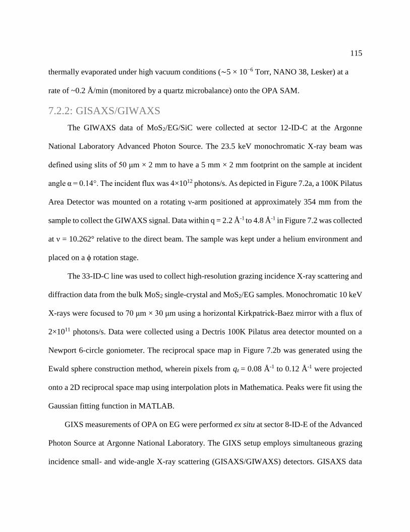
115
thermally evaporated under high vacuum conditions (∼5 × 10⁻⁶ Torr, NANO 38, Lesker) at a
rate of ~0.2 Å/min (monitored by a quartz microbalance) onto the OPA SAM.
7.2.2: GISAXS/GIWAXS
The GIWAXS data of MoS2/EG/SiC were collected at sector 12-ID-C at the Argonne
National Laboratory Advanced Photon Source. The 23.5 keV monochromatic X-ray beam was
defined using slits of 50 μm × 2 mm to have a 5 mm × 2 mm footprint on the sample at incident
angle α = 0.14°. The incident flux was 4×10¹² photons/s. As depicted in Figure 7.2a, a 100K Pilatus
Area Detector was mounted on a rotating ν-arm positioned at approximately 354 mm from the
sample to collect the GIWAXS signal. Data within q = 2.2 Å-1 to 4.8 Å-1 in Figure 7.2 was collected
at ν = 10.262° relative to the direct beam. The sample was kept under a helium environment and
placed on a ϕ rotation stage.
The 33-ID-C line was used to collect high-resolution grazing incidence X-ray scattering and
diffraction data from the bulk MoS2 single-crystal and MoS2/EG samples. Monochromatic 10 keV
X-rays were focused to 70 μm × 30 μm using a horizontal Kirkpatrick-Baez mirror with a flux of
2×10¹¹ photons/s. Data were collected using a Dectris 100K Pilatus area detector mounted on a
Newport 6-circle goniometer. The reciprocal space map in Figure 7.2b was generated using the
Ewald sphere construction method, wherein pixels from qz = 0.08 Å-1 to 0.12 Å-1 were projected
onto a 2D reciprocal space map using interpolation plots in Mathematica. Peaks were fit using the
Gaussian fitting function in MATLAB.
GIXS measurements of OPA on EG were performed ex situ at sector 8-ID-E of the Advanced
Photon Source at Argonne National Laboratory. The GIXS setup employs simultaneous grazing
incidence small- and wide-angle X-ray scattering (GISAXS/GIWAXS) detectors. GISAXS data
116
was collected for |Qmax| < 2 nm-1 with a Pilatus 1M detector and GIWAXS data was collected in
regions for Q > 2 nm-1 with a Pilatus 100K offset horizontally from the direct beam. Sector 8-ID-
E employed polarized monochromatic 7.35 keV x-rays through a beam defining slit 40 μm by 500
μm with incident photon flux of ~1011 photons/s. Samples were mounted on a φ-rotatable vacuum
stage and 100 s exposures were taken every 1.0°. The incident angle was set at α = 0.26°,
approximately 70% of the critical angle of the SiC substrate. The GISAXS experimental geometry
was calibrated using a silver behenate standard. The data were analyzed using the NIKA software
package from Argonne along with MATLAB and Mathematica fitting routines.
7.2.3: XRR
7.3: High-resolution X-ray measurements were performed at the Advanced Photon Source (APS)
station 33ID-D of Argonne National Laboratory. XRR were collected for the as-grown
EG/SiC(0001) and MoS2 on EG/SiC(0001) samples. Monochromatic 10.00 keV (wavelength λ =
0.1240 nm) X-rays were focused to 70 μm × 30 μm using a Kirkpatrick-Baez mirror with a flux
of 2×10¹¹ photons/s. To reduce oxidation, the sample was kept in a He/H atmosphere. Data were
collected using a Dectris 100K Pilatus area detector mounted on a Newport 6-circle goniometer.
The XRR intensities from the area detector were extracted following established experimental
methods provided in Refs. [137,199].
7.4: Results
7.4.1: In-plane structure
CVD growth of MoS2 on EG is performed at a variety of conditions in order to tune and
optimize the MoS2 film thickness. Figures 7.1b,c are AFM topography and phase images,
respectively, of MoS2 grown on EG at 43 Torr. Figure 7.1d extracts the edge orientations of the
117
MoS2 triangles shown in Figure 7.1b by plotting a line along one edge of each triangle. A large
majority of the triangles have parallel edges as indicated by the blue lines, while a few triangles,
indicated in red, have edges rotated by 30°. The rare occurrence of a third rotational orientation of
a MoS2 triangular domain is shown in pink. From this analysis, it is apparent that there are two
predominant types of azimuthal registration of MoS2 on EG. This crystal orientation alignment is
attributed to van der Waals epitaxy [52], which accommodates the large lattice mismatch (~28%)
between graphene and MoS2, as will be further discussed below.
Figure 7.1: CVD-grown MoS2 on EG grown at 43 Torr. (a) AFM height and (b) phase images of
MoS2/EG. Line profiles show monolayer MoS2 (green) and graphene (red) thicknesses. The
contrast between bilayer and monolayer regions of EG is more obvious in the phase image. (c)
Extraction of edge orientations of MoS2 crystals in (a) showing two predominant registrations of
MoS2 on EG.
To verify that these local AFM and STM observations persist over the entire sample,
synchrotron grazing incidence wide-angle X-ray scattering (GIWAXS) is employed to investigate
the van der Waals epitaxy of MoS2 on EG. A schematic of GIWAXS is shown in Figure 7.2a and
experimental details are outlined in the Methods section. In GIWAXS, the incident X-ray beam is
at incident angle α = 0.14°, slightly below the critical angle of total external reflection of the
substrate. The out-of-plane angle β and in-plane angle 2ϕ define the position at which the scattered
118
X-ray wave vector kf intersects the plane of the 2D detector. The qxy 2D reciprocal space map of
the MoS2/EG/SiC structure projected from qz = 0.08 Å-1 to 0.12 Å-1 is shown in Figure 7.2b with
first order spots of MoS2, EG, and SiC identified. The blue, orange, and magenta arrows indicate
the reciprocal lattice vectors b* for MoS2, EG, and SiC, respectively. As seen by the reciprocal
space points, the reciprocal lattices for MoS2 and EG are aligned, whereas SiC has a well-known
30° rotation with respect to EG [221]. This observation indicates that the majority of the MoS2
crystals are epitaxially grown along the EG lattice direction with matching six-fold symmetry,
confirming the symmetry inferred from AFM (Figure 7.2). The real-space structure reconstructed
for such aligned MoS2 growth is shown in Figure 7.2c, where the two MoS2 triangles represent the
preferred orientations in the epitaxial MoS2/EG heterostructure. Projected first order MoS2 and
SiC peaks onto ϕ are included in Figure 7.2d to examine the angular distribution. The relative
angle between the MoS2 and SiC lattices is indeed 30°±0.3°, which is a much narrower azimuthal
distribution than that of CVD MoS2 grown on sapphire [222]. The full-width-at-half-maxima of
the first order MoS2, EG, and SiC peaks as a function of ϕ are 0.7°, 0.5°, and 0.05° (limited by X-
ray optics), respectively, which confirms that the MoS2 is in good registry with EG.
Figure 7.2e shows the scattered intensity from the 2D reciprocal space map of Figure 7.2b
collected along qy at qx = 0. The real-space lattice constants calculated for MoS2, EG, and SiC are
3.16±0.01 Å, 2.46±0.01 Å and 3.07±0.01 Å, respectively. To gain more insight into the structure
of MoS2 on EG, in-plane GIXD of MoS2/EG and bulk MoS2 was performed (Figure 7.2). The
resulting lattice constants of MoS2/EG and bulk MoS2 are 3.160±0.005 Å and 3.159±0.006 Å,
which indicate a relaxed in-plane structure of MoS2 on EG similar to its bulk counterpart. The lack
of in-plane strain in the synthesized MoS2 2D crystals can be explained by total strain relaxation
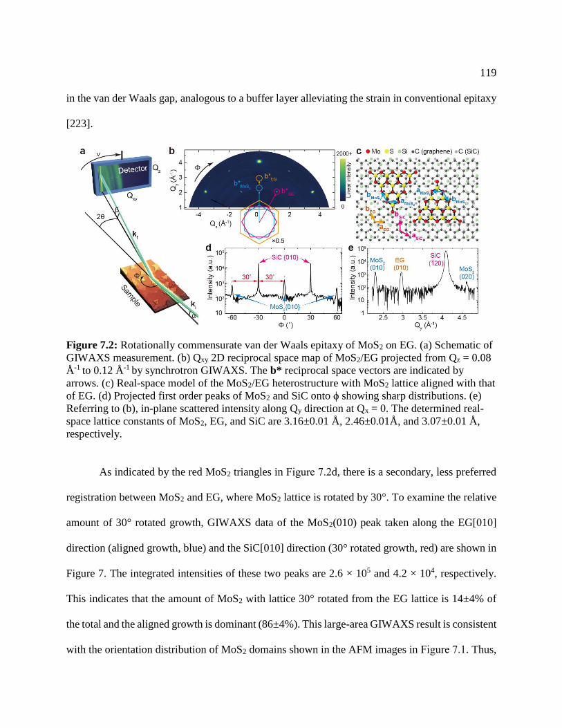
119
in the van der Waals gap, analogous to a buffer layer alleviating the strain in conventional epitaxy
[223].
Figure 7.2: Rotationally commensurate van der Waals epitaxy of MoS2 on EG. (a) Schematic of
GIWAXS measurement. (b) Qxy 2D reciprocal space map of MoS2/EG projected from Qz = 0.08
Å-1 to 0.12 Å-1 by synchrotron GIWAXS. The b* reciprocal space vectors are indicated by
arrows. (c) Real-space model of the MoS2/EG heterostructure with MoS2 lattice aligned with that
of EG. (d) Projected first order peaks of MoS2 and SiC onto ϕ showing sharp distributions. (e)
Referring to (b), in-plane scattered intensity along Qy direction at Qx = 0. The determined real-
space lattice constants of MoS2, EG, and SiC are 3.16±0.01 Å, 2.46±0.01Å, and 3.07±0.01 Å,
respectively.
As indicated by the red MoS2 triangles in Figure 7.2d, there is a secondary, less preferred
registration between MoS2 and EG, where MoS2 lattice is rotated by 30°. To examine the relative
amount of 30° rotated growth, GIWAXS data of the MoS2(010) peak taken along the EG[010]
direction (aligned growth, blue) and the SiC[010] direction (30° rotated growth, red) are shown in
Figure 7. The integrated intensities of these two peaks are 2.6 × 10⁵ and 4.2 × 10⁴, respectively.
This indicates that the amount of MoS2 with lattice 30° rotated from the EG lattice is 14±4% of
the total and the aligned growth is dominant (86±4%). This large-area GIWAXS result is consistent
with the orientation distribution of MoS2 domains shown in the AFM images in Figure 7.1. Thus,
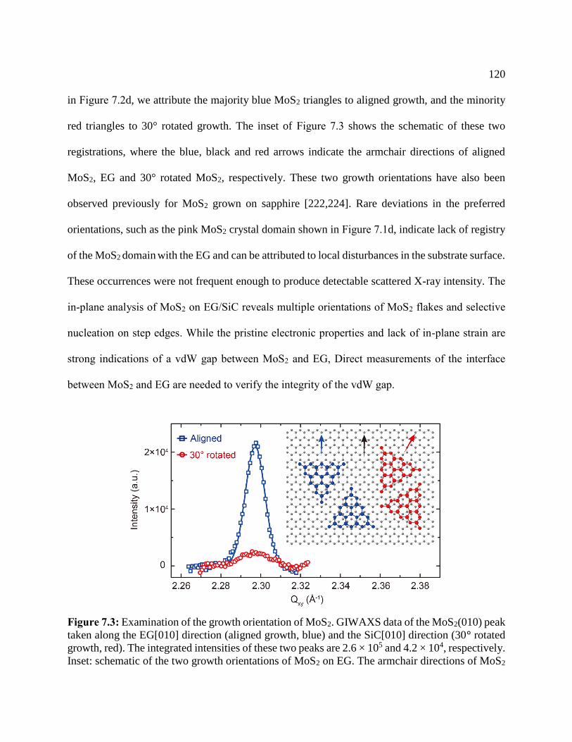
120
in Figure 7.2d, we attribute the majority blue MoS2 triangles to aligned growth, and the minority
red triangles to 30° rotated growth. The inset of Figure 7.3 shows the schematic of these two
registrations, where the blue, black and red arrows indicate the armchair directions of aligned
MoS2, EG and 30° rotated MoS2, respectively. These two growth orientations have also been
observed previously for MoS2 grown on sapphire [222,224]. Rare deviations in the preferred
orientations, such as the pink MoS2 crystal domain shown in Figure 7.1d, indicate lack of registry
of the MoS2 domain with the EG and can be attributed to local disturbances in the substrate surface.
These occurrences were not frequent enough to produce detectable scattered X-ray intensity. The
in-plane analysis of MoS2 on EG/SiC reveals multiple orientations of MoS2 flakes and selective
nucleation on step edges. While the pristine electronic properties and lack of in-plane strain are
strong indications of a vdW gap between MoS2 and EG, Direct measurements of the interface
between MoS2 and EG are needed to verify the integrity of the vdW gap.
Figure 7.3: Examination of the growth orientation of MoS2. GIWAXS data of the MoS2(010) peak
taken along the EG[010] direction (aligned growth, blue) and the SiC[010] direction (30° rotated
growth, red). The integrated intensities of these two peaks are 2.6 × 10⁵ and 4.2 × 10⁴, respectively.
Inset: schematic of the two growth orientations of MoS2 on EG. The armchair directions of MoS2

121
from aligned (blue) and 30° rotated (red) growth are indicated by the blue and red arrows,
respectively. The black arrow indicates the armchair direction of EG.
7.4.2: Vertical Model
XRR was employed to probe the interface between MoS2 and the underlying EG/SiC.
Generating a model from X-ray reflectivity, being an ensemble averaging of all layered structures
on the sample surface, necessitates the use of a model which captures all these layered structures
simultaneous, reflected in the measured XRR data. The model consists of layers of distinct
elements described by their height above the semi-infinite SiC(0001) surface, z, fractional
monolayer occupancy, Θ, and distribution width, u. Following previous XRR analysis of EG/SiC
[134], the SiC substrate contained four relaxed adlayers of alternating C and Si atop a semi-infinite
bulk 4H-SiC(0001) (Si-terminated) substrate. Three overlaying graphene layers (EG1-3) rested atop
an EG0 buffer layer consisting of two distinct C positions. To account for the CVD grown MoS2
atop the few-layer graphene on SiC(0001), six MoS2 layers were added to the EG/SiC system, of
which three MoS2 layers [(MoS2)1-3] were assumed to be sitting atop EG1-3 with and vdW gap and
the other three MoS2 layers reflect the fractional coverage of bilayer MoS2 seen in AFM [106].
Physical constraints were applied to the parameters (z, Θ, and u) to obtain a reasonable
model fit. The stoichiometry of each MoS2 layer was fixed, so a single occupancy Θ parameter
was used for one Mo and surrounding two S layers in a single MoS2 layer. The covalent
interactions between Mo and S were assumed to be bulk-like (Mo-S vertical separation = 1.5 Å)
and identical for each MoS2 layer. The occupancy for a given (MoS2)n layer was assumed to be
no greater than the exposed surface of the corresponding EGn layer, where the fraction of exposed
surface is given by Θn - Θn+1 for EGn. Likewise, physically related parameters were described with
a single viable to reduce the large number of free parameters (~192) used to describe this system.

122
7.4.3: Vertical Structure
Figure 7.4: XRR data of (a) EG/SiC, (b) CVD-deposited MoS2 on EG/SiC, and (c) EG/SiC
following MoS2 transfer. XRR data show with black dots and accompanying error bars, model fit
with red line, and simulated XRR for an ideal bulk terminated 4H-SiC(0001) surface with a dashed
line. (d-f) The XRR model fit derived electron density profile along the [0001] direction.
The XRR derived model fits of EG on SiC(0001) (Figure 7.4d) show exceptional
agreement with previously reported values [14,88]. The peaks present at 1.9 Å-1, 3.7 Å-1, and 5.6
Å-1 correspond to the 3.3 A d-spacing of graphene. The EG0 layer is comprised of a 40±10%
covalently bonded C layer and 60±10% relaxed C layer resting 2.1±0.1 Å and 2.4±0.1 Å,
respectively, above the terminus Si layer of SiC. The gap between the overlaying graphene (EG1-
3), closely match values expected from bulk (3.4±0.2 Å). The distribution width (0.16±0.2 Å)
confirms EG1-3 are pristine graphene layers.
The addition of CVD deposited MoS2 is accompanied by additional undulations in the XRR
data. The C-C peaks at 1.9 Å-1, 3.7 Å-1, and 5.6 Å-1 remain, confirming the few-layer graphene
a b c
d e f

123
remains pristine after deposition. New sharp undulations present at 1.0 Å-1 and 3.1 Å-1 are primarily
accounted for by Mo-Mo spacing (5.9±0.2 Å) which correspond to the formation of few-layer
MoS2 as seen by AFM. These primary features show additional modulations from Mo-C spacing
and from the two S layers which accompany each Mo layer in MoS2. To model the presence of
MoS2, the parameters for EG/SiC(0001) were initially held at fixed values, then relaxed to achieve
a best fit. The underlying EG2-3 are unchanged following MoS2 deposition, and (MoS2)2-3 on EG2-
3 show a vdW gap separation of 4.6±0.3 Å with 20±6% MoS2 coverage. Bulk-like bilayer MoS2
covers the sample with 34±4% of the (MoS2)1-3 forming a bilayer.
Significant changes to the model were needed at the region near the interface, consisting
of EG0-1, to achieve a good fit. The two distinct carbon peaks that makeup EG0 shifted outward to
2.3±0.1 Å and 2.5±0.1 Å, and their distribution width decreased to (~0.08 Å) and (~0.2 Å). While
the overlaying EG1 layer broadened in distribution width (~0.4 Å). This abnormality in EG1 was
further accompanied by a substantially higher (MoS2)1 coverage (88±9%) suggesting a
considerably higher degree of interaction between MoS2 on EG1 than on the more graphitic EG2-3
layers. This disproportionately high coverage could be has been reported in previous work on
MoS2 on EG/SiC [225], which shows the formation of near unity coverage MoS2 specifically on
EG1, and multilayers MoS2 were only observed atop defective graphene. However, this
observation does not fully explain our results and is inconsistent with our AFM data [106].
To verify the chemical integrity of the MoS2 and EG/SiC XPS data was taken before and
after MoS2 deposition. The Mo 3d and S 2p peaks showed no notable deviation from bulk-like
MoS2, while the C 1s peak is inconclusive owing to the large number of distinct C chemical states
present in EG/SiC [14]. The lack of strong covalent chemistry suggests the changes to the interface
124
are induced through vdW interactions between layers. The structure of the EG0 buffer layer has
previously been shown to be highly sensitive to the stabilizing influence of EG1 [88]. While the
weak electronic screening of graphene allows interfaces on either side of graphene to interaction
through graphene [50]. Thus, MoS2 interactions with the EG0 buffer layer through EG1 would not
be without precedent.
However, complications arise when considering the EG0 buffer layer, as subtle changes to
the interface will have an enhanced impact on the measured XRR by the presence of MoS2. While
it has been clear since early CTR investigations of this interface that he EG0 layer is sitting at a
much-reduced distance (~2.2 Å) [134], the precise structure of this interface has undergone
continued scrutiny [14,88]. The study performed by Emery [14], utilized XRR measurements
enhanced with chemically specific XSW-XPS data, to reveal 2 distinct chemical states of C within
EG0 corresponding to a more sp3-hybridized C at 2.1±0.1 Å and a more sp2-hybridized C at
2.45±0.10 Å. Another XRR and XSW-XPS study performed by Conrad [88] proposes an interface
structure with 3 distinct C state that transforms with the formation of additional EG layers atop
EG0.
Ultimately, our investigation of the influence of MoS2 on EG/SiC cannot be conclusive,
because the transformation seen at the interface between EG and SiC(0001) with the addition of
MoS2 could either reflect 1) a structural change in the EG/SiC to accommodate the addition of
epitaxial MoS2 or 2) imperfect modeling of the EG/SiC interface, which only becomes evident
with the addition of MoS2.
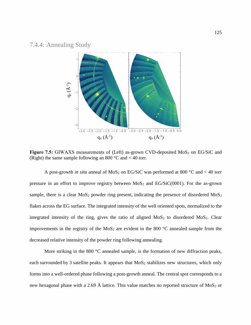
125
7.4.4: Annealing Study
Figure 7.5: GIWAXS measurements of (Left) as-grown CVD-deposited MoS2 on EG/SiC and
(Right) the same sample following an 800 °C and < 40 torr.
A post-growth in situ anneal of MoS2 on EG/SiC was performed at 800 °C and < 40 torr
pressure in an effort to improve registry between MoS2 and EG/SiC(0001). For the as-grown
sample, there is a clear MoS2 powder ring present, indicating the presence of disordered MoS2
flakes across the EG surface. The integrated intensity of the well oriented spots, normalized to the
integrated intensity of the ring, gives the ratio of aligned MoS2 to disordered MoS2. Clear
improvements in the registry of the MoS2 are evident in the 800 °C annealed sample from the
decreased relative intensity of the powder ring following annealing.
More striking in the 800 °C annealed sample, is the formation of new diffraction peaks,
each surrounded by 3 satellite peaks. It appears that MoS2 stabilizes new structures, which only
forms into a well-ordered phase following a post-growth anneal. The central spot corresponds to a
new hexagonal phase with a 2.69 Å lattice. This value matches no reported structure of MoS2 or
qy (
Å-1
)
qx (Å-1) qx (Å
-1)
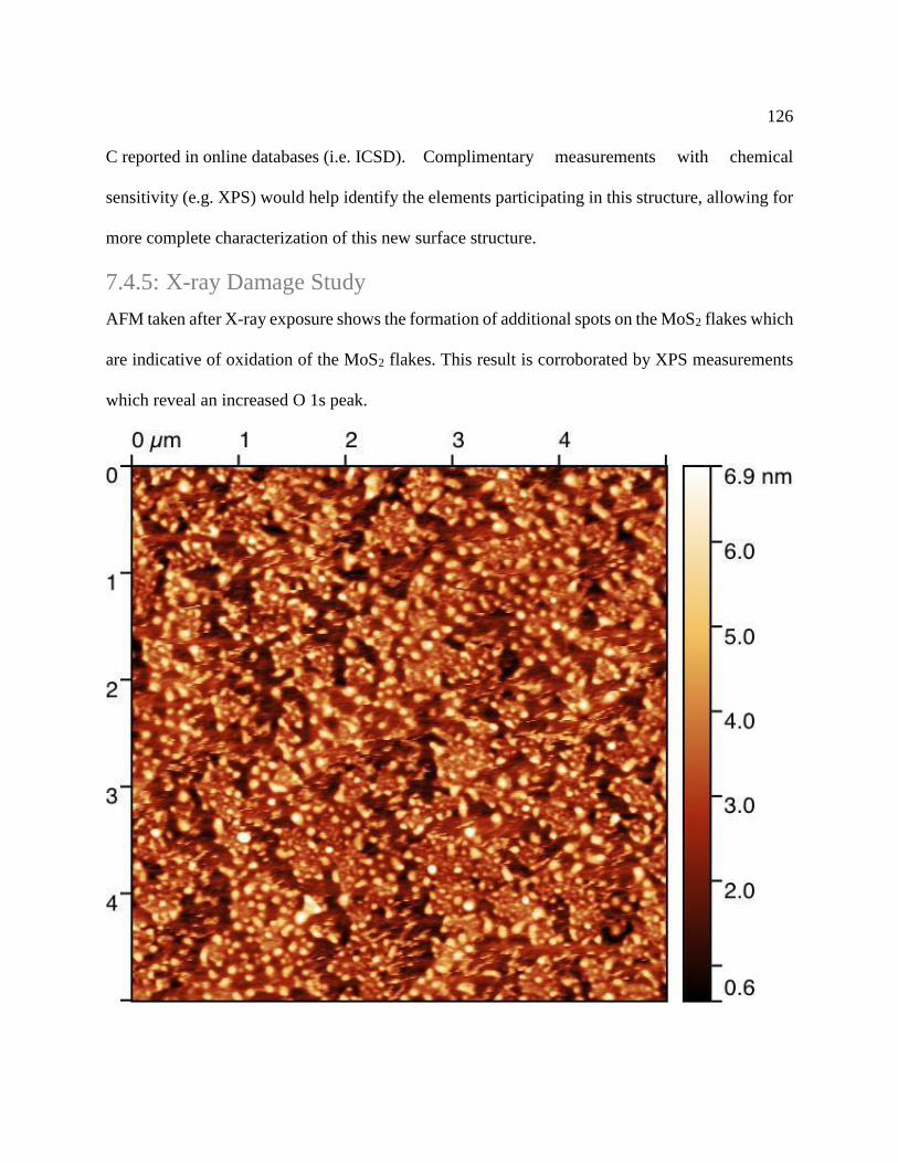
126
C reported in online databases (i.e. ICSD). Complimentary measurements with chemical
sensitivity (e.g. XPS) would help identify the elements participating in this structure, allowing for
more complete characterization of this new surface structure.
7.4.5: X-ray Damage Study
AFM taken after X-ray exposure shows the formation of additional spots on the MoS2 flakes which
are indicative of oxidation of the MoS2 flakes. This result is corroborated by XPS measurements
which reveal an increased O 1s peak.

127
Figure 7.6: AFM of degraded MoS2 flakes on EG/SiC after hours of exposure to the unattenuated
X-ray beam at 33-ID-D. (AFM image provided by J.I. Balla and X. Liu)
7.4.6: Organic molecules on EG/SiC
Figure 7.7: AFM of MMS. (a) AFM of OPA SAM on EG. The two domain oriention differ by
~64°. The SAM is continuous over EG/SiC step edges, indicated by green arrows. Fourier
transform (inset, scale bar is 1 nm-1) corresponds to a corrugation periodicity of 5.5 ± 0.3 nm. (b)
Schematic cross section of OPA on EG/SiC. Bottom to top: 4H-SiC (blue and grey), carbon-rich
buffer layer SiC (6√3 × 6√3)R30° surface reconstruction (maroon), graphene layer (purple), and
two neighboring OPA molecules with hydrogen bonds between phosphonic acid headgroups.
(AFM image provided by J.I. Balla and X. Liu)

128
We extended synchrotron grazing incidence small-angle X-ray scattering (GISAXS) and
grazing incidence wide-angle X-ray scattering (GIWAXS) analysis to examine the registry of 1D
heterostructures [226]. Here we investigated the structure of metal deposited on OPA molecules
or metalized molecular stripes (MMS). The real space model of the assembly overlaid with the
graphene (green), SiC (pink) and MMS (blue) lattice vectors is shown in Figure 7.8a. The
corresponding 2D reciprocal space map of platinum MMS is produced from GISAXS images
collected as a function of azimuthal angle φ in Figure 7.8b. The six MMS {10} Bragg peaks on
the map are formed from the superposition of 3 MMS domain orientations. To examine the relative
orientations of the MMS domains, an intensity profile cut along the φ direction of the reciprocal
space map is fitted with Gaussians and included in Figure 7.8c. The MMS scattered intensity
reaches a maximum every 60±2° indicating that the MMS domains are conformal to the 6-fold
symmetry of the underlying graphene in agreement with the AFM observations. To determine the
orientation of the 1D MMS domains with respect to the underlying substrate, GIWAXS data is
acquired simultaneously with the GISAXS experiment and provides the coordinates of the SiC
{101} Bragg peaks, from which the aSiC in-plane direction can be extracted. The Ewald sphere
construction method is used to convert raw GISAXS and GIWAXS data into reciprocal space as
shown in Figure 7.8c for direct comparison. The SiC {101} Bragg peaks are aligned relative to the
MMS {10} peaks in Figure 7.8c. In real space, this corresponds to a 30° rotation [221,227] between
the aSiC and aMSS and a parallel alignment between aMMS and aEG real space vectors (Figure 7.8a),
indicating that the metal stripes are laying along the EG “arm-chair” direction. MMS spacing and
domain structure were calculated from the integrated intensity along the longitudinal (𝐿) path of
the reciprocal space map as shown in Figure 7.8d. The 5.41±0.05 nm spacing between the platinum
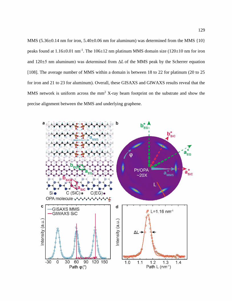
129
MMS (5.36±0.14 nm for iron, 5.40±0.06 nm for aluminum) was determined from the MMS {10}
peaks found at 1.16±0.01 nm-1. The 106±12 nm platinum MMS domain size (120±10 nm for iron
and 120±5 nm aluminum) was determined from ΔL of the MMS peak by the Scherrer equation
[108]. The average number of MMS within a domain is between 18 to 22 for platinum (20 to 25
for iron and 21 to 23 for aluminum). Overall, these GISAXS and GIWAXS results reveal that the
MMS network is uniform across the mm2 X-ray beam footprint on the substrate and show the
precise alignment between the MMS and underlying graphene.

130
Figure 7.8: Grazing incidence small and wide-angle X-ray scattering. (a) Top view of the
assembly in real space overlaid with the graphene (green), SiC (pink) and MMS (grey) unit cell
vectors. (The MMS vector extends much longer than shown.) (b) A corresponding 2D reciprocal
space map of platinum MMS overlaid with the respective reciprocal unit vectors of panel (a) (the
2D reciprocal space map is scaled by ~20× for clarity). (c) GISAXS intensity profile cut (light
blue) from panel (b) along the φ direction (blue) showing maximum intensity at 60°± 2° intervals.
The GISAXS plot is overlaid with GIWAXS SiC {101} Bragg peaks (pink) indicating the direction
of the MMS with respect to the substrate. (d) Intensity profile cut from panel (b) along the 𝐿 path
allowing determination of MMS spacing.
7.5: Conclusions
In summary, a 2D heterostructure of rotationally commensurate MoS2 on EG has been
grown via van der Waals epitaxy with controlled thickness. The structural and electronic quality
of these samples has been probed down to the atomic scale using a combination of horizontally
and vertically sensitive synchrotron X-ray scattering techniques. MoS2 is found to preferentially
grow with lattice aligned with EG. The relative amount of a less preferred registry is also
determined. Furthermore, in-plane X-ray diffraction show that the MoS2 is nearly strain-free, thus
providing an ideal system for probing the fundamental properties of two-dimensional MoS2. This
in addition to our OPA study suggests that EG may be a promising substrate for van der Waals
epitaxial growth of other emerging two-dimensional nanomaterials in addition to providing a well-
defined platform for the future study and application of MoS2/graphene heterostructures.
131
Chapter 8: Future Work
8.1: Borophene on Au(111)
Early theoretical work predicted stable forms of 2D boron on the (111) faces Au, Ag, Cu,
and Ni [49]. Of these, borophene has only been successful grown on Ag(111) [5,6], leaving Au,
Cu and Ni yet to be explored. Of these metals, Au(111) is the only surface to show a lowest energy
v1/9 in-plane structure and 1.1 Å vertically buckled structure, making it distinct from the measured
borophene phases on Ag(111). This structure reflects the weaker interaction between the v1/9 phase
and Au (77 meV/atom) compared to the v1/6 phase on Ag (175 meV), explained by weakening of
the substrate interactions with the reduction of fractional vacancies in the borophene. The weaken
substrate interactions are reflected in the vertical position of the borophene above the substrate,
this weakening trend was theoretically predicted for v1/6 and v1/5 phases of borophene, however the
vertical positions of the v1/6 and v1/5 phases appear identical in our XSW measurements.
Synthesizing polymorphs of borophene with drastically different vacancy configurations would
enable us to explore theoretical predictions of borophene substrate interactions with more certainty
and provide valuable insight into 2D boron polymorphism.
8.2: Blue Phosphorus
2D forms of phosphorus were first isolated by mechanical exfoliation of bulk black
phosphorus (BP) [228]. Bulk BP has long been known to exhibit high degrees of polymorphism
[41], showing reversible transitions to an arsenic and simple-cubic crystal structure [43]. Blue
phosphorus, along with 2 other structural derivates by geometrical tweaks to BP, were predicated
to from layered stable free-standing monolayers [228]. Blue phosphorus was recently synthesized
at the 2D limit on Au (111) using molecular beam epitaxy under ultra-high vacuum [44].
132
STM reveals a 2D diamond structure, which appears in (4x4) registry with the underlying
Au(111) and (5x5) registry with the proposed model for blue phosphorus. The proposed
superstructure model contains 42 P atoms, 24 of which rest 2.40 Å above the Au(111) and 18
vertically buckled outward at 3.58 Å above the Au(111). The in-plane structure is believed to be
somewhat strained to accommodate a slight lattice mismatch between the structure of blue
phosphorus and the underlying Au(111). Dark lines are seen in the STM data, which are reflected
in the simulations by a relaxation of the bottom layer as well as omitted rows of top layer atoms.
Interestingly, this structure deviates considerably from measurements and simulations of bulk blue
phosphorus [41,43], suggesting strong interactions at the interface which could be investigated
further through chemically resolved structural measurements using synchrotron X-rays.
133
References:
[1] A. H. Castro Neto, F. Guinea, N. M. R. Peres, K. S. Novoselov, and A. K. Geim, The
Electronic Properties of Graphene, Reviews of Modern Physics 81, 109 (2009).
[2] Y. Zhang, V. W. Brar, C. Girit, A. Zettl, and M. F. Crommie, Origin of Spatial Charge
Inhomogeneity in Graphene, Nature Physics 5, 722 (2009).
[3] A. K. Newaz, Y. S. Puzyrev, B. Wang, S. T. Pantelides, and K. I. Bolotin, Probing
Charge Scattering Mechanisms in Suspended Graphene by Varying Its Dielectric Environment,
Nat Commun 3, 734, 734 (2012).
[4] Z. Y. Al Balushi, K. Wang, R. K. Ghosh, R. A. Vila, S. M. Eichfeld, J. D. Caldwell, X.
Qin, Y. C. Lin, P. A. DeSario, G. Stone, S. Subramanian, D. F. Paul, R. M. Wallace, S. Datta, J.
M. Redwing, and J. A. Robinson, Two-Dimensional Gallium Nitride Realized Via Graphene
Encapsulation, Nat Mater 15, 1166 (2016).
[5] B. Feng, J. Zhang, Q. Zhong, W. Li, S. Li, H. Li, P. Cheng, S. Meng, L. Chen, and K.
Wu, Experimental Realization of Two-Dimensional Boron Sheets, Nat Chem 8, 563 (2016).
[6] A. J. Mannix, X. F. Zhou, B. Kiraly, J. D. Wood, D. Alducin, B. D. Myers, X. Liu, B. L.
Fisher, U. Santiago, J. R. Guest, M. J. Yacaman, A. Ponce, A. R. Oganov, M. C. Hersam, and N.
P. Guisinger, Synthesis of Borophenes: Anisotropic, Two-Dimensional Boron Polymorphs,
Science 350, 1513 (2015).
[7] P. Vogt, P. De Padova, C. Quaresima, J. Avila, E. Frantzeskakis, M. C. Asensio, A.
Resta, B. Ealet, and G. Le Lay, Silicene: Compelling Experimental Evidence for Graphenelike
Two-Dimensional Silicon, Phys Rev Lett 108, 155501 (2012).
[8] A. J. Mannix, B. Kiraly, B. L. Fisher, M. C. Hersam, and N. P. Guisinger, Silicon Growth
at the Two-Dimensional Limit on Ag(111), ACS Nano 8, 7538 (2014).
[9] Y. Chen, M. W. Gramlich, S. T. Hayden, and P. F. Miceli, In Situx-Ray Scattering Study
of Ag Island Growth on Si(111)7×7, Physical Review B 94, 11, 045437 (2016).
[10] M. Satta, S. Colonna, R. Flammini, A. Cricenti, and F. Ronci, Silicon Reactivity at the
Ag(111) Surface, Phys Rev Lett 115, 026102, 026102 (2015).
[11] A. K. Geim, Graphene: Status and Prospects, Science 324, 1530 (2009).
[12] C. R. Dean, A. F. Young, I. Meric, C. Lee, L. Wang, S. Sorgenfrei, K. Watanabe, T.
Taniguchi, P. Kim, K. L. Shepard, and J. Hone, Boron Nitride Substrates for High-Quality
Graphene Electronics, Nat Nanotechnol 5, 722 (2010).
[13] J. H. Chen, C. Jang, S. Xiao, M. Ishigami, and M. S. Fuhrer, Intrinsic and Extrinsic
Performance Limits of Graphene Devices on Sio2, Nat Nanotechnol 3, 206 (2008).
[14] J. D. Emery, B. Detlefs, H. J. Karmel, L. O. Nyakiti, D. K. Gaskill, M. C. Hersam, J.
Zegenhagen, and M. J. Bedzyk, Chemically Resolved Interface Structure of Epitaxial Graphene
on Sic(0001), Phys Rev Lett 111, 215501 (2013).
[15] J. C. Meyer, A. K. Geim, M. I. Katsnelson, K. S. Novoselov, T. J. Booth, and S. Roth,
The Structure of Suspended Graphene Sheets, Nature 446, 60 (2007).
[16] J. C. Shelton, H. R. Patil, and J. M. Blakely, Equilibrium Segregation of Carbon to a
Nickel (111) Surface: A Surface Phase Transition, Surface Science 43, 493 (1974).
134
[17] T. A. Land, T. Michely, R. J. Behm, J. C. Hemminger, and G. Comsa, Stm Investigation
of Single Layer Graphite Structures Produced on Pt(111) by Hydrocarbon Decomposition,
Surface Science 264, 261 (1992).
[18] M. Eizenberg and J. M. Blakely, Carbon Interaction with Nickel Surfaces: Monolayer
Formation and Structural Stability, The Journal of Chemical Physics 71, 3467 (1979).
[19] I. Forbeaux, J. M. Themlin, and J. M. Debever, Heteroepitaxial Graphite
On6h−Sic(0001): Interface Formation through Conduction-Band Electronic Structure, Physical
Review B 58, 16396 (1998).
[20] N. D. Mermin, Crystalline Order in Two Dimensions, Physical Review 176, 250 (1968).
[21] K. S. Novoselov, A. K. Geim, S. V. Morozov, D. Jiang, Y. Zhang, S. V. Dubonos, I. V.
Grigorieva, and A. A. Firsov, Electric Field Effect in Atomically Thin Carbon Films, Science
306, 666 (2004).
[22] X. Li, W. Cai, J. An, S. Kim, J. Nah, D. Yang, R. Piner, A. Velamakanni, I. Jung, E.
Tutuc, S. K. Banerjee, L. Colombo, and R. S. Ruoff, Large-Area Synthesis of High-Quality and
Uniform Graphene Films on Copper Foils, Science 324, 1312 (2009).
[23] J.-H. Lee, E. K. Lee, W.-J. Joo, Y. Jang, B.-S. Kim, J. Y. Lim, S.-H. Choi, S. J. Ahn, J.
R. Ahn, M.-H. Park, C.-W. Yang, B. L. Choi, S.-W. Hwang, and D. Whang, Wafer-Scale
Growth of Single-Crystal Monolayer Graphene on Reusable Hydrogen-Terminated Germanium,
Science 344, 286 (2014).
[24] X. Li, W. Cai, J. An, S. Kim, J. Nah, D. Yang, R. Piner, A. Velamakanni, I. Jung, E.
Tutuc, S. K. Banerjee, L. Colombo, and R. S. Ruoff, Large-Area Synthesis of High-Quality and
Uniform Graphene Films on Copper Foils, Science 324, 1312 (2009).
[25] J. N. Coleman, M. Lotya, A. O'Neill, S. D. Bergin, P. J. King, U. Khan, K. Young, A.
Gaucher, S. De, R. J. Smith, I. V. Shvets, S. K. Arora, G. Stanton, H. Y. Kim, K. Lee, G. T. Kim,
G. S. Duesberg, T. Hallam, J. J. Boland, J. J. Wang, J. F. Donegan, J. C. Grunlan, G. Moriarty,
A. Shmeliov, R. J. Nicholls, J. M. Perkins, E. M. Grieveson, K. Theuwissen, D. W. McComb, P.
D. Nellist, and V. Nicolosi, Two-Dimensional Nanosheets Produced by Liquid Exfoliation of
Layered Materials, Science 331, 568 (2011).
[26] J. Kang, J. W. Seo, D. Alducin, A. Ponce, M. J. Yacaman, and M. C. Hersam, Thickness
Sorting of Two-Dimensional Transition Metal Dichalcogenides Via Copolymer-Assisted Density
Gradient Ultracentrifugation, Nat Commun 5, 5478, 5478 (2014).
[27] E. Grånäs, T. Gerber, U. A. Schröder, K. Schulte, J. N. Andersen, T. Michely, and J.
Knudsen, Hydrogen Intercalation under Graphene on Ir(111), Surface Science 651, 57 (2016).
[28] C. Lee, X. Wei, J. W. Kysar, and J. Hone, Measurement of the Elastic Properties and
Intrinsic Strength of Monolayer Graphene, Science 321, 385 (2008).
[29] R. R. Nair, P. Blake, A. N. Grigorenko, K. S. Novoselov, T. J. Booth, T. Stauber, N. M.
Peres, and A. K. Geim, Fine Structure Constant Defines Visual Transparency of Graphene,
Science 320, 1308 (2008).
[30] A. K. Geim and K. S. Novoselov, The Rise of Graphene, Nat Mater 6, 183 (2007).
[31] T. Bjorkman, A. Gulans, A. V. Krasheninnikov, and R. M. Nieminen, Van Der Waals
Bonding in Layered Compounds from Advanced Density-Functional First-Principles
Calculations, Physical Review Letters 108, 5, 235502 (2012).
[32] H. W. Kroto, J. R. Heath, S. C. O'Brien, R. F. Curl, and R. E. Smalley, C60:
Buckminsterfullerene, Nature 318, 162 (1985).
135
[33] S. Iijima, Helical Microtubules of Graphitic Carbon, Nature 354, 56 (1991).
[34] B. T. Kiraly, Northwestern University, 2016.
[35] Y. Zhang, Y. W. Tan, H. L. Stormer, and P. Kim, Experimental Observation of the
Quantum Hall Effect and Berry's Phase in Graphene, Nature 438, 201 (2005).
[36] G. W. Semenoff, Condensed-Matter Simulation of a Three-Dimensional Anomaly,
Physical Review Letters 53, 2449 (1984).
[37] E. Fradkin, Critical Behavior of Disordered Degenerate Semiconductors. Ii. Spectrum
and Transport Properties in Mean-Field Theory, Phys Rev B Condens Matter 33, 3263 (1986).
[38] F. D. Haldane, Model for a Quantum Hall Effect without Landau Levels: Condensed-
Matter Realization of the "Parity Anomaly", Phys Rev Lett 61, 2015 (1988).
[39] K. Takeda and K. Shiraishi, Theoretical Possibility of Stage Corrugation in Si and Ge
Analogs of Graphite, Phys Rev B Condens Matter 50, 14916 (1994).
[40] S. Cahangirov, M. Topsakal, E. Akturk, H. Sahin, and S. Ciraci, Two- and One-
Dimensional Honeycomb Structures of Silicon and Germanium, Phys Rev Lett 102, 236804,
236804 (2009).
[41] J. C. Jamieson, Crystal Structures Adopted by Black Phosphorus at High Pressures,
Science 139, 1291 (1963).
[42] J. Guan, Z. Zhu, and D. Tomanek, Phase Coexistence and Metal-Insulator Transition in
Few-Layer Phosphorene: A Computational Study, Phys Rev Lett 113, 046804 (2014).
[43] S. E. Boulfelfel, G. Seifert, Y. Grin, and S. Leoni, Squeezing Lone Pairs: The A17 to A7
Pressure-Induced Phase Transition in Black Phosphorus, Physical Review B 85, 6, 014110
(2012).
[44] J. L. Zhang, S. Zhao, C. Han, Z. Wang, S. Zhong, S. Sun, R. Guo, X. Zhou, C. D. Gu, K.
D. Yuan, Z. Li, and W. Chen, Epitaxial Growth of Single Layer Blue Phosphorus: A New Phase
of Two-Dimensional Phosphorus, Nano Lett 16, 4903 (2016).
[45] M. Wu, H. Fu, L. Zhou, K. Yao, and X. C. Zeng, Nine New Phosphorene Polymorphs
with Non-Honeycomb Structures: A Much Extended Family, Nano Lett 15, 3557 (2015).
[46] B. Feng, Z. Ding, S. Meng, Y. Yao, X. He, P. Cheng, L. Chen, and K. Wu, Evidence of
Silicene in Honeycomb Structures of Silicon on Ag(111), Nano Lett 12, 3507 (2012).
[47] S. Cahangirov, V. O. Özçelik, L. Xian, J. Avila, S. Cho, M. C. Asensio, S. Ciraci, and A.
Rubio, Atomic Structure of The3×3phase of Silicene on Ag(111), Physical Review B 90, 035448
(2014).
[48] E. Vlieg, E. Fontes, and J. R. Patel, Structure Analysis of Si(111)-(√3 × √3 )R30°/Ag
Using X-Ray Standing Waves, Physical Review B 43, 7185 (1991).
[49] Z. Zhang, Y. Yang, G. Gao, and B. I. Yakobson, Two-Dimensional Boron Monolayers
Mediated by Metal Substrates, Angew Chem Int Ed Engl 54, 13022 (2015).
[50] Y. Kim, S. S. Cruz, K. Lee, B. O. Alawode, C. Choi, Y. Song, J. M. Johnson, C.
Heidelberger, W. Kong, S. Choi, K. Qiao, I. Almansouri, E. A. Fitzgerald, J. Kong, A. M.
Kolpak, J. Hwang, and J. Kim, Remote Epitaxy through Graphene Enables Two-Dimensional
Material-Based Layer Transfer, Nature 544, 340 (2017).
[51] K. V. Emtsev, F. Speck, T. Seyller, L. Ley, and J. D. Riley, Interaction, Growth, and
Ordering of Epitaxial Graphene on Sic{0001} Surfaces: A Comparative Photoelectron
Spectroscopy Study, Physical Review B 77 (2008).
136
[52] A. Koma, Vanderwaals Epitaxy - a New Epitaxial-Growth Method for a Highly Lattice-
Mismatched System, Thin Solid Films 216, 72 (1992).
[53] M. Xu, T. Liang, M. Shi, and H. Chen, Graphene-Like Two-Dimensional Materials,
Chem Rev 113, 3766 (2013).
[54] M. Ishigami, J. H. Chen, W. G. Cullen, M. S. Fuhrer, and E. D. Williams, Atomic
Structure of Graphene on Sio2, Nano Lett 7, 1643 (2007).
[55] C. R. Dean, A. F. Young, I. Meric, C. Lee, L. Wang, S. Sorgenfrei, K. Watanabe, T.
Taniguchi, P. Kim, K. L. Shepard, and J. Hone, Boron Nitride Substrates for High-Quality
Graphene Electronics, Nature Nanotechnology 5, 722 (2010).
[56] A. M. Shikin, D. Farías, and K. H. Rieder, Phonon Stiffening Induced by Copper
Intercalation in Monolayer Graphite on Ni(111), Europhysics Letters (EPL) 44, 44 (1998).
[57] Y. Gamo, A. Nagashima, M. Wakabayashi, M. Terai, and C. Oshima, Atomic Structure
of Monolayer Graphite Formed on Ni(111), Surface Science 374, 61 (1997).
[58] A. Varykhalov, J. Sanchez-Barriga, A. M. Shikin, C. Biswas, E. Vescovo, A. Rybkin, D.
Marchenko, and O. Rader, Electronic and Magnetic Properties of Quasifreestanding Graphene on
Ni, Phys Rev Lett 101, 157601, 157601 (2008).
[59] H. Tetlow, J. Posthuma de Boer, I. J. Ford, D. D. Vvedensky, J. Coraux, and L.
Kantorovich, Growth of Epitaxial Graphene: Theory and Experiment, Physics Reports 542, 195
(2014).
[60] M. Batzill, The Surface Science of Graphene: Metal Interfaces, Cvd Synthesis,
Nanoribbons, Chemical Modifications, and Defects, Surface Science Reports 67, 83 (2012).
[61] C. Riedl, C. Coletti, and U. Starke, Structural and Electronic Properties of Epitaxial
Graphene on Sic(0 0 0 1): A Review of Growth, Characterization, Transfer Doping and
Hydrogen Intercalation, Journal of Physics D: Applied Physics 43, 374009 (2010).
[62] W. Norimatsu and M. Kusunoki, Epitaxial Graphene on Sic{0001}: Advances and
Perspectives, Phys Chem Chem Phys 16, 3501 (2014).
[63] A. B. Preobrajenski, M. L. Ng, A. S. Vinogradov, and N. Martensson, Controlling
Graphene Corrugation on Lattice-Mismatched Substrates, Physical Review B 78, 4, 073401
(2008).
[64] D. Eom, D. Prezzi, K. T. Rim, H. Zhou, M. Lefenfeld, S. Xiao, C. Nuckolls, M. S.
Hybertsen, T. F. Heinz, and G. W. Flynn, Structure and Electronic Properties of Graphene
Nanoislands on Co(0001), Nano Lett 9, 2844 (2009).
[65] W. Moritz, B. Wang, M. L. Bocquet, T. Brugger, T. Greber, J. Wintterlin, and S.
Gunther, Structure Determination of the Coincidence Phase of Graphene on Ru(0001), Phys Rev
Lett 104, 136102, 136102 (2010).
[66] D. Martoccia, P. R. Willmott, T. Brugger, M. Bjorck, S. Gunther, C. M. Schleputz, A.
Cervellino, S. A. Pauli, B. D. Patterson, S. Marchini, J. Wintterlin, W. Moritz, and T. Greber,
Graphene on Ru(0001): A 25 X 25 Supercell, Phys Rev Lett 101, 126102, 126102 (2008).
[67] B. Wang, M. Caffio, C. Bromley, H. Fruchtl, and R. Schaub, Coupling Epitaxy, Chemical
Bonding, and Work Function at the Local Scale in Transition Metal-Supported Graphene, ACS
Nano 4, 5773 (2010).
[68] E. Miniussi, M. Pozzo, A. Baraldi, E. Vesselli, R. R. Zhan, G. Comelli, T. O. Mentes, M.
A. Nino, A. Locatelli, S. Lizzit, and D. Alfe, Thermal Stability of Corrugated Epitaxial Graphene
Grown on Re(0001), Phys Rev Lett 106, 216101, 216101 (2011).

137
[69] Q. J. Wang and J. G. Che, Origins of Distinctly Different Behaviors of Pd and Pt
Contacts on Graphene, Phys Rev Lett 103, 066802, 066802 (2009).
[70] G. Giovannetti, P. A. Khomyakov, G. Brocks, V. M. Karpan, J. van den Brink, and P. J.
Kelly, Doping Graphene with Metal Contacts, Phys Rev Lett 101, 026803, 026803 (2008).
[71] P. Sutter, J. T. Sadowski, and E. Sutter, Graphene on Pt(111): Growth and Substrate
Interaction, Physical Review B 80, 245411 (2009).
[72] C. Gong, G. Lee, B. Shan, E. M. Vogel, R. M. Wallace, and K. Cho, First-Principles
Study of Metal–Graphene Interfaces, Journal of Applied Physics 108, 123711 (2010).
[73] M. Vanin, J. J. Mortensen, A. K. Kelkkanen, J. M. Garcia-Lastra, K. S. Thygesen, and K.
W. Jacobsen, Graphene on Metals: A Van Der Waals Density Functional Study, Physical Review
B 81, 081408 (2010).
[74] C. Busse, P. Lazic, R. Djemour, J. Coraux, T. Gerber, N. Atodiresei, V. Caciuc, R.
Brako, A. T. N'Diaye, S. Blugel, J. Zegenhagen, and T. Michely, Graphene on Ir(111):
Physisorption with Chemical Modulation, Phys Rev Lett 107, 036101, 036101 (2011).
[75] N. A. Vinogradov, A. A. Zakharov, V. Kocevski, J. Rusz, K. A. Simonov, O. Eriksson,
A. Mikkelsen, E. Lundgren, A. S. Vinogradov, N. Martensson, and A. B. Preobrajenski,
Formation and Structure of Graphene Waves on Fe(110), Phys Rev Lett 109, 026101, 026101
(2012).
[76] B. Hammer and J. K. Norskov, in Advances in Catalysis, Vol 45: Impact of Surface
Science on Catalysis, edited by B. C. Gates, and H. Knozinger2000), pp. 71.
[77] J. J. McCarroll, T. Edmonds, and R. C. Pitkethly, Interpretation of a Complex Low
Energy Electron Diffraction Pattern: Carbonaceous and Sulphur-Containing Structures on
Ni(111), Nature 223, 1260 (1969).
[78] C. Klink, I. Stensgaard, F. Besenbacher, and E. Lægsgaard, An Stm Study of Carbon-
Induced Structures on Ni(111): Evidence for a Carbidic-Phase Clock Reconstruction, Surface
Science 342, 250 (1995).
[79] F. Mittendorfer, A. Garhofer, J. Redinger, J. Klimes, J. Harl, and G. Kresse, Graphene on
Ni(111): Strong Interaction and Weak Adsorption, Physical Review B 84, 201401 (2011).
[80] L. Gao, J. R. Guest, and N. P. Guisinger, Epitaxial Graphene on Cu(111), Nano Lett 10,
3512 (2010).
[81] J. H. Lee, E. K. Lee, W. J. Joo, Y. Jang, B. S. Kim, J. Y. Lim, S. H. Choi, S. J. Ahn, J. R.
Ahn, M. H. Park, C. W. Yang, B. L. Choi, S. W. Hwang, and D. Whang, Wafer-Scale Growth of
Single-Crystal Monolayer Graphene on Reusable Hydrogen-Terminated Germanium, Science
344, 286 (2014).
[82] B. Kiraly, R. M. Jacobberger, A. J. Mannix, G. P. Campbell, M. J. Bedzyk, M. S. Arnold,
M. C. Hersam, and N. P. Guisinger, Electronic and Mechanical Properties of Graphene-
Germanium Interfaces Grown by Chemical Vapor Deposition, Nano Lett 15, 7414 (2015).
[83] J. Dai, D. Wang, M. Zhang, T. Niu, A. Li, M. Ye, S. Qiao, G. Ding, X. Xie, Y. Wang, P.
K. Chu, Q. Yuan, Z. Di, X. Wang, F. Ding, and B. I. Yakobson, How Graphene Islands Are
Unidirectionally Aligned on the Ge(110) Surface, Nano Lett 16, 3160 (2016).
[84] R. Rojas Delgado, R. M. Jacobberger, S. S. Roy, V. S. Mangu, M. S. Arnold, F. Cavallo,
and M. G. Lagally, Passivation of Germanium by Graphene, ACS Appl Mater Interfaces 9,
17629 (2017).

138
[85] R. I. Scace and G. A. Slack, Solubility of Carbon in Silicon and Germanium, The Journal
of Chemical Physics 30, 1551 (1959).
[86] W. Strupinski, K. Grodecki, A. Wysmolek, R. Stepniewski, T. Szkopek, P. E. Gaskell, A.
Gruneis, D. Haberer, R. Bozek, J. Krupka, and J. M. Baranowski, Graphene Epitaxy by
Chemical Vapor Deposition on Sic, Nano Lett 11, 1786 (2011).
[87] A. Al-Temimy, C. Riedl, and U. Starke, Low Temperature Growth of Epitaxial Graphene
on Sic Induced by Carbon Evaporation, Applied Physics Letters 95, 3, 231907 (2009).
[88] M. Conrad, J. Rault, Y. Utsumi, Y. Garreau, A. Vlad, A. Coati, J. P. Rueff, P. F. Miceli,
and E. H. Conrad, Structure and Evolution of Semiconducting Buffer Graphene Grown on
Sic(0001), Physical Review B 96, 12, 195304 (2017).
[89] W. A. de Heer, C. Berger, X. Wu, P. N. First, E. H. Conrad, X. Li, T. Li, M. Sprinkle, J.
Hass, M. L. Sadowski, M. Potemski, and G. Martinez, Epitaxial Graphene, Solid State
Communications 143, 92 (2007).
[90] C. Virojanadara, M. Syväjarvi, R. Yakimova, L. I. Johansson, A. A. Zakharov, and T.
Balasubramanian, Homogeneous Large-Area Graphene Layer Growth On6h-Sic(0001), Physical
Review B 78, 245403 (2008).
[91] R. M. Tromp and J. B. Hannon, Thermodynamics and Kinetics of Graphene Growth on
Sic(0001), Phys Rev Lett 102, 106104, 106104 (2009).
[92] K. V. Emtsev, A. Bostwick, K. Horn, J. Jobst, G. L. Kellogg, L. Ley, J. L. McChesney,
T. Ohta, S. A. Reshanov, J. Rohrl, E. Rotenberg, A. K. Schmid, D. Waldmann, H. B. Weber, and
T. Seyller, Towards Wafer-Size Graphene Layers by Atmospheric Pressure Graphitization of
Silicon Carbide, Nat Mater 8, 203 (2009).
[93] E. S. Penev, S. Bhowmick, A. Sadrzadeh, and B. I. Yakobson, Polymorphism of Two-
Dimensional Boron, Nano Lett 12, 2441 (2012).
[94] H. Tang and S. Ismail-Beigi, Novel Precursors for Boron Nanotubes: The Competition of
Two-Center and Three-Center Bonding in Boron Sheets, Phys Rev Lett 99, 115501 (2007).
[95] B. Feng, J. Zhang, R.-Y. Liu, T. Iimori, C. Lian, H. Li, L. Chen, K. Wu, S. Meng, F.
Komori, and I. Matsuda, Direct Evidence of Metallic Bands in a Monolayer Boron Sheet,
Physical Review B 94, 041408 (2016).
[96] E. S. Penev, A. Kutana, and B. I. Yakobson, Can Two-Dimensional Boron
Superconduct?, Nano Lett 16, 2522 (2016).
[97] Y. Zhao, S. Zeng, and J. Ni, Superconductivity in Two-Dimensional Boron Allotropes,
Physical Review B 93, 014502 (2016).
[98] Y. Liu, E. S. Penev, and B. I. Yakobson, Probing the Synthesis of Two-Dimensional
Boron by First-Principles Computations, Angew Chem Int Ed Engl 52, 3156 (2013).
[99] Q. Zhong, J. Zhang, P. Cheng, B. Feng, W. Li, S. Sheng, H. Li, S. Meng, L. Chen, and K.
Wu, Metastable Phases of 2d Boron Sheets on Ag(1 1 1), J Phys Condens Matter 29, 095002
(2017).
[100] Z. Zhang, A. J. Mannix, Z. Hu, B. Kiraly, N. P. Guisinger, M. C. Hersam, and B. I.
Yakobson, Substrate-Induced Nanoscale Undulations of Borophene on Silver, Nano Lett 16,
6622 (2016).
[101] Z. Zhang, E. S. Penev, and B. I. Yakobson, Two-Dimensional Materials: Polyphony in B
Flat, Nat Chem 8, 525 (2016).

139
[102] X. Yang, Y. Ding, and J. Ni, Ab Initioprediction of Stable Boron Sheets and Boron
Nanotubes: Structure, Stability, and Electronic Properties, Physical Review B 77, 041402 (2008).
[103] Z. Zhang, E. S. Penev, and B. I. Yakobson, Two-Dimensional Boron: Structures,
Properties and Applications, Chem Soc Rev 46, 6746 (2017).
[104] A. J. Mannix, B. Kiraly, M. C. Hersam, and N. P. Guisinger, Synthesis and Chemistry of
Elemental 2d Materials, Nat. Rev. Chem. 1, 14, 0014 (2017).
[105] A. K. Geim and I. V. Grigorieva, Van Der Waals Heterostructures, Nature 499, 419
(2013).
[106] X. Liu, I. Balla, H. Bergeron, G. P. Campbell, M. J. Bedzyk, and M. C. Hersam,
Rotationally Commensurate Growth of Mos2 on Epitaxial Graphene, ACS Nano 10, 1067
(2016).
[107] Y. Shi, W. Zhou, A. Y. Lu, W. Fang, Y. H. Lee, A. L. Hsu, S. M. Kim, K. K. Kim, H. Y.
Yang, L. J. Li, J. C. Idrobo, and J. Kong, Van Der Waals Epitaxy of Mos(2) Layers Using
Graphene as Growth Templates, Nano Lett 12, 2784 (2012).
[108] B. E. Warren, X-Ray Diffraction (Dover Publications, 1969).
[109] J. Als-Nielsen and D. McMorrow, in Elements of Modern X-Ray Physics (John Wiley &
Sons, Inc., 2011), pp. 113.
[110] J. Woicik, Hard X-Ray Photoelectron Spectroscopy (Haxpes) 2016), Springer Series in
Surface Sciences.
[111] J. D. Watson and F. H. Crick, Molecular Structure of Nucleic Acids; a Structure for
Deoxyribose Nucleic Acid, Nature 171, 737 (1953).
[112] B. W. Batterman, Effect of Thermal Vibrations on Diffraction from Perfect Crystals. Ii.
The Bragg Case of Reflection, Physical Review 127, 686 (1962).
[113] B. Okkerse, Anomalous Transmission of X-Rays in Germanium .1. Imaginary Part of
Atomic Scattering Factor, Philips Research Reports 17, 464 (1962).
[114] B. W. Batterman and H. Cole, Dynamical Diffraction of X Rays by Perfect Crystals,
Reviews of Modern Physics 36, 681 (1964).
[115] N. Kato, Dynamical Diffraction Theory of Waves in Distorted Crystals. I. General
Formulation and Treatment for Perfect Crystals, Acta Crystallographica 16, 276 (1963).
[116] N. Kato, Dynamical Diffraction Theory of Waves in Distorted Crystals. Ii. Perturbation
Theory, Acta Crystallographica 16, 282 (1963).
[117] C. J. Fisher, R. Ithin, R. G. Jones, G. J. Jackson, D. P. Woodruff, and B. C. C. Cowie,
Non-Dipole Photoemission Effects in X-Ray Standing Wavefield Determination of Surface
Structure, Journal of Physics: Condensed Matter 10, L623 (1998).
[118] F. Schreiber, K. A. Ritley, I. A. Vartanyants, H. Dosch, J. Zegenhagen, and B. C. C.
Cowie, Non-Dipolar Contributions in Xps Detection of X-Ray Standing Waves, Surface Science
486, L519 (2001).
[119] G. van Straaten, M. Franke, F. C. Bocquet, F. S. Tautz, and C. Kumpf, Non-Dipolar
Effects in Photoelectron-Based Normal Incidence X-Ray Standing Wave Experiments, Journal
of Electron Spectroscopy and Related Phenomena 222, 106 (2018).
[120] F. H. Farwick Zum Hagen, D. M. Zimmermann, C. C. Silva, C. Schlueter, N. Atodiresei,
W. Jolie, A. J. Martinez-Galera, D. Dombrowski, U. A. Schroder, M. Will, P. Lazic, V. Caciuc,
S. Blugel, T. L. Lee, T. Michely, and C. Busse, Structure and Growth of Hexagonal Boron
Nitride on Ir(111), ACS Nano 10, 11012 (2016).
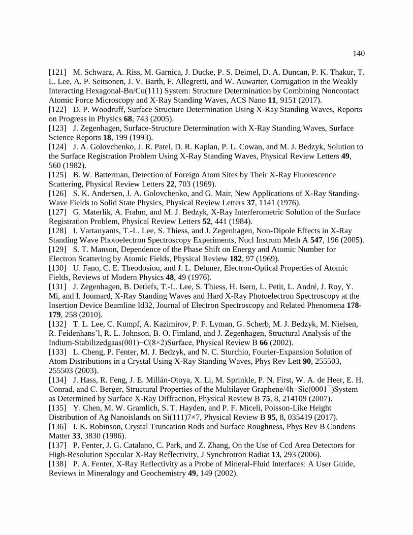
140
[121] M. Schwarz, A. Riss, M. Garnica, J. Ducke, P. S. Deimel, D. A. Duncan, P. K. Thakur, T.
L. Lee, A. P. Seitsonen, J. V. Barth, F. Allegretti, and W. Auwarter, Corrugation in the Weakly
Interacting Hexagonal-Bn/Cu(111) System: Structure Determination by Combining Noncontact
Atomic Force Microscopy and X-Ray Standing Waves, ACS Nano 11, 9151 (2017).
[122] D. P. Woodruff, Surface Structure Determination Using X-Ray Standing Waves, Reports
on Progress in Physics 68, 743 (2005).
[123] J. Zegenhagen, Surface-Structure Determination with X-Ray Standing Waves, Surface
Science Reports 18, 199 (1993).
[124] J. A. Golovchenko, J. R. Patel, D. R. Kaplan, P. L. Cowan, and M. J. Bedzyk, Solution to
the Surface Registration Problem Using X-Ray Standing Waves, Physical Review Letters 49,
560 (1982).
[125] B. W. Batterman, Detection of Foreign Atom Sites by Their X-Ray Fluorescence
Scattering, Physical Review Letters 22, 703 (1969).
[126] S. K. Andersen, J. A. Golovchenko, and G. Mair, New Applications of X-Ray Standing-
Wave Fields to Solid State Physics, Physical Review Letters 37, 1141 (1976).
[127] G. Materlik, A. Frahm, and M. J. Bedzyk, X-Ray Interferometric Solution of the Surface
Registration Problem, Physical Review Letters 52, 441 (1984).
[128] I. Vartanyants, T.-L. Lee, S. Thiess, and J. Zegenhagen, Non-Dipole Effects in X-Ray
Standing Wave Photoelectron Spectroscopy Experiments, Nucl Instrum Meth A 547, 196 (2005).
[129] S. T. Manson, Dependence of the Phase Shift on Energy and Atomic Number for
Electron Scattering by Atomic Fields, Physical Review 182, 97 (1969).
[130] U. Fano, C. E. Theodosiou, and J. L. Dehmer, Electron-Optical Properties of Atomic
Fields, Reviews of Modern Physics 48, 49 (1976).
[131] J. Zegenhagen, B. Detlefs, T.-L. Lee, S. Thiess, H. Isern, L. Petit, L. André, J. Roy, Y.
Mi, and I. Joumard, X-Ray Standing Waves and Hard X-Ray Photoelectron Spectroscopy at the
Insertion Device Beamline Id32, Journal of Electron Spectroscopy and Related Phenomena 178-
179, 258 (2010).
[132] T. L. Lee, C. Kumpf, A. Kazimirov, P. F. Lyman, G. Scherb, M. J. Bedzyk, M. Nielsen,
R. Feidenhans’l, R. L. Johnson, B. O. Fimland, and J. Zegenhagen, Structural Analysis of the
Indium-Stabilizedgaas(001)−C(8×2)Surface, Physical Review B 66 (2002).
[133] L. Cheng, P. Fenter, M. J. Bedzyk, and N. C. Sturchio, Fourier-Expansion Solution of
Atom Distributions in a Crystal Using X-Ray Standing Waves, Phys Rev Lett 90, 255503,
255503 (2003).
[134] J. Hass, R. Feng, J. E. Millán-Otoya, X. Li, M. Sprinkle, P. N. First, W. A. de Heer, E. H.
Conrad, and C. Berger, Structural Properties of the Multilayer Graphene/4h−Sic(0001¯)System
as Determined by Surface X-Ray Diffraction, Physical Review B 75, 8, 214109 (2007).
[135] Y. Chen, M. W. Gramlich, S. T. Hayden, and P. F. Miceli, Poisson-Like Height
Distribution of Ag Nanoislands on Si(111)7×7, Physical Review B 95, 8, 035419 (2017).
[136] I. K. Robinson, Crystal Truncation Rods and Surface Roughness, Phys Rev B Condens
Matter 33, 3830 (1986).
[137] P. Fenter, J. G. Catalano, C. Park, and Z. Zhang, On the Use of Ccd Area Detectors for
High-Resolution Specular X-Ray Reflectivity, J Synchrotron Radiat 13, 293 (2006).
[138] P. A. Fenter, X-Ray Reflectivity as a Probe of Mineral-Fluid Interfaces: A User Guide,
Reviews in Mineralogy and Geochemistry 49, 149 (2002).
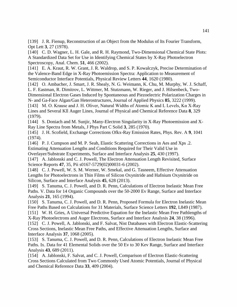
141
[139] J. R. Fienup, Reconstruction of an Object from the Modulus of Its Fourier Transform,
Opt Lett 3, 27 (1978).
[140] C. D. Wagner, L. H. Gale, and R. H. Raymond, Two-Dimensional Chemical State Plots:
A Standardized Data Set for Use in Identifying Chemical States by X-Ray Photoelectron
Spectroscopy, Anal. Chem. 51, 466 (2002).
[141] E. A. Kraut, R. W. Grant, J. R. Waldrop, and S. P. Kowalczyk, Precise Determination of
the Valence-Band Edge in X-Ray Photoemission Spectra: Application to Measurement of
Semiconductor Interface Potentials, Physical Review Letters 44, 1620 (1980).
[142] O. Ambacher, J. Smart, J. R. Shealy, N. G. Weimann, K. Chu, M. Murphy, W. J. Schaff,
L. F. Eastman, R. Dimitrov, L. Wittmer, M. Stutzmann, W. Rieger, and J. Hilsenbeck, Two-
Dimensional Electron Gases Induced by Spontaneous and Piezoelectric Polarization Charges in
N- and Ga-Face Algan/Gan Heterostructures, Journal of Applied Physics 85, 3222 (1999).
[143] M. O. Krause and J. H. Oliver, Natural Widths of Atomic K and L Levels, Kα X‐Ray
Lines and Several Kll Auger Lines, Journal of Physical and Chemical Reference Data 8, 329
(1979).
[144] S. Doniach and M. Sunjic, Many-Electron Singularity in X-Ray Photoemission and X-
Ray Line Spectra from Metals, J Phys Part C Solid 3, 285 (1970).
[145] J. H. Scofield, Exchange Corrections Ofkx-Ray Emission Rates, Phys. Rev. A 9, 1041
(1974).
[146] P. J. Cumpson and M. P. Seah, Elastic Scattering Corrections in Aes and Xps .2.
Estimating Attenuation Lengths and Conditions Required for Their Valid Use in
Overlayer/Substrate Experiments, Surface and Interface Analysis 25, 430 (1997).
[147] A. Jablonski and C. J. Powell, The Electron Attenuation Length Revisited, Surface
Science Reports 47, 35, Pii s0167-5729(02)00031-6 (2002).
[148] C. J. Powell, W. S. M. Werner, W. Smekal, and G. Tasneem, Effective Attenuation
Lengths for Photoelectrons in Thin Films of Silicon Oxynitride and Hafnium Oxynitride on
Silicon, Surface and Interface Analysis 45, 628 (2013).
[149] S. Tanuma, C. J. Powell, and D. R. Penn, Calculations of Electron Inelastic Mean Free
Paths. V. Data for 14 Organic Compounds over the 50-2000 Ev Range, Surface and Interface
Analysis 21, 165 (1994).
[150] S. Tanuma, C. J. Powell, and D. R. Penn, Proposed Formula for Electron Inelastic Mean
Free Paths Based on Calculations for 31 Materials, Surface Science Letters 192, L849 (1987).
[151] W. H. Gries, A Universal Predictive Equation for the Inelastic Mean Free Pathlengths of
X-Ray Photoelectrons and Auger Electrons, Surface and Interface Analysis 24, 38 (1996).
[152] C. J. Powell, A. Jablonski, and F. Salvat, Nist Databases with Electron Elastic-Scattering
Cross Sections, Inelastic Mean Free Paths, and Effective Attenuation Lengths, Surface and
Interface Analysis 37, 1068 (2005).
[153] S. Tanuma, C. J. Powell, and D. R. Penn, Calculations of Electron Inelastic Mean Free
Paths. Ix. Data for 41 Elemental Solids over the 50 Ev to 30 Kev Range, Surface and Interface
Analysis 43, 689 (2011).
[154] A. Jablonski, F. Salvat, and C. J. Powell, Comparison of Electron Elastic-Scattering
Cross Sections Calculated from Two Commonly Used Atomic Potentials, Journal of Physical
and Chemical Reference Data 33, 409 (2004).

142
[155] A. Jablonski and C. J. Powell, Practical Expressions for the Mean Escape Depth, the
Information Depth, and the Effective Attenuation Length in Auger-Electron Spectroscopy and X-
Ray Photoelectron Spectroscopy, Journal of Vacuum Science & Technology A: Vacuum,
Surfaces, and Films 27, 253 (2009).
[156] J. H. Hubbell, P. N. Trehan, N. Singh, B. Chand, D. Mehta, M. L. Garg, R. R. Garg, S.
Singh, and S. Puri, A Review, Bibliography, and Tabulation of K, L, and Higher Atomic Shell
X‐Ray Fluorescence Yields, Journal of Physical and Chemical Reference Data 23, 339 (1994).
[157] E. Zanazzi and F. Jona, A Reliability Factor for Surface Structure Determinations by
Low-Energy Electron Diffraction, Surface Science 62, 61 (1977).
[158] T. Ogitsu, E. Schwegler, and G. Galli, Beta-Rhombohedral Boron: At the Crossroads of
the Chemistry of Boron and the Physics of Frustration, Chem Rev 113, 3425 (2013).
[159] A. P. Sergeeva, I. A. Popov, Z. A. Piazza, W. L. Li, C. Romanescu, L. S. Wang, and A. I.
Boldyrev, Understanding Boron through Size-Selected Clusters: Structure, Chemical Bonding,
and Fluxionality, Acc Chem Res 47, 1349 (2014).
[160] K. S. Novoselov, D. Jiang, F. Schedin, T. J. Booth, V. V. Khotkevich, S. V. Morozov,
and A. K. Geim, Two-Dimensional Atomic Crystals, Proc Natl Acad Sci U S A 102, 10451
(2005).
[161] Q. H. Wang, K. Kalantar-Zadeh, A. Kis, J. N. Coleman, and M. S. Strano, Electronics
and Optoelectronics of Two-Dimensional Transition Metal Dichalcogenides, Nat Nanotechnol 7,
699 (2012).
[162] X. Ling, H. Wang, S. Huang, F. Xia, and M. S. Dresselhaus, The Renaissance of Black
Phosphorus, Proc Natl Acad Sci U S A 112, 4523 (2015).
[163] Z. A. Piazza, H. S. Hu, W. L. Li, Y. F. Zhao, J. Li, and L. S. Wang, Planar Hexagonal
B(36) as a Potential Basis for Extended Single-Atom Layer Boron Sheets, Nat Commun 5, 3113,
3113 (2014).
[164] I. Boustani, Systematic Ab Initio Investigation of Bare Boron Clusters:Mdetermination of
the Geometryand Electronic Structures Ofbn(N=2–14), Physical Review B 55, 16426 (1997).
[165] X. Wu, J. Dai, Y. Zhao, Z. Zhuo, J. Yang, and X. C. Zeng, Two-Dimensional Boron
Monolayer Sheets, ACS Nano 6, 7443 (2012).
[166] F. Bianchini, L. L. Patera, M. Peressi, C. Africh, and G. Comelli, Atomic Scale
Identification of Coexisting Graphene Structures on Ni(111), J Phys Chem Lett 5, 467 (2014).
[167] J. Zegenhagen, Surface Structure Determination with X-Ray Standing Waves, Surface
Science Reports 18, 202 (1993).
[168] A. J. Mannix, B. Kiraly, M. C. Hersam, and N. P. Guisinger, Synthesis and Chemistry of
Elemental 2d Materials, Nat Rev Chem 1, 1 (2017).
[169] I09 Beamline Layout, http://www.diamond.ac.uk/Beamlines/Surfaces-and-
Interfaces/I09/Beamline-layout.html (2018).
[170] B. Feng, O. Sugino, R. Y. Liu, J. Zhang, R. Yukawa, M. Kawamura, T. Iimori, H. Kim,
Y. Hasegawa, H. Li, L. Chen, K. Wu, H. Kumigashira, F. Komori, T. C. Chiang, S. Meng, and I.
Matsuda, Dirac Fermions in Borophene, Phys Rev Lett 118, 096401 (2017).
[171] N. A. Fairley, Casaxps, Casa Software Limited, 2016.
[172] C. J. Powell and A. Jablonski, Electron Effective Attenuation Lengths for Applications in
Auger Electron Spectroscopy and X-Ray Photoelectron Spectroscopy, Surface and Interface
Analysis 33, 211 (2002).
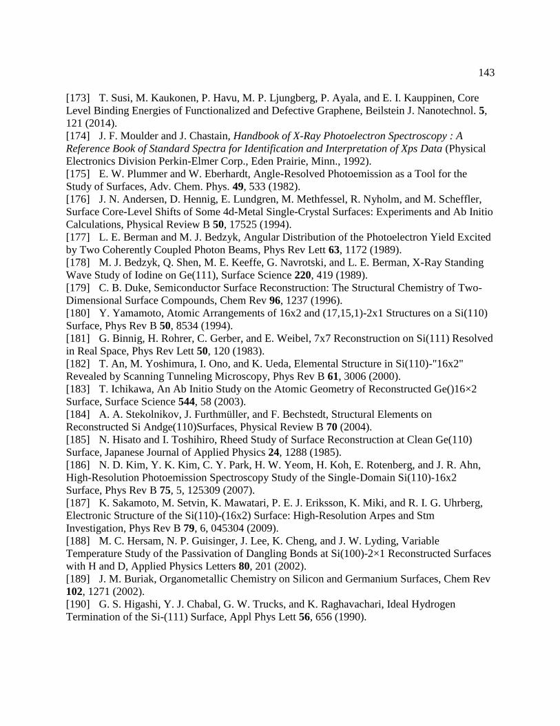
143
[173] T. Susi, M. Kaukonen, P. Havu, M. P. Ljungberg, P. Ayala, and E. I. Kauppinen, Core
Level Binding Energies of Functionalized and Defective Graphene, Beilstein J. Nanotechnol. 5,
121 (2014).
[174] J. F. Moulder and J. Chastain, Handbook of X-Ray Photoelectron Spectroscopy : A
Reference Book of Standard Spectra for Identification and Interpretation of Xps Data (Physical
Electronics Division Perkin-Elmer Corp., Eden Prairie, Minn., 1992).
[175] E. W. Plummer and W. Eberhardt, Angle-Resolved Photoemission as a Tool for the
Study of Surfaces, Adv. Chem. Phys. 49, 533 (1982).
[176] J. N. Andersen, D. Hennig, E. Lundgren, M. Methfessel, R. Nyholm, and M. Scheffler,
Surface Core-Level Shifts of Some 4d-Metal Single-Crystal Surfaces: Experiments and Ab Initio
Calculations, Physical Review B 50, 17525 (1994).
[177] L. E. Berman and M. J. Bedzyk, Angular Distribution of the Photoelectron Yield Excited
by Two Coherently Coupled Photon Beams, Phys Rev Lett 63, 1172 (1989).
[178] M. J. Bedzyk, Q. Shen, M. E. Keeffe, G. Navrotski, and L. E. Berman, X-Ray Standing
Wave Study of Iodine on Ge(111), Surface Science 220, 419 (1989).
[179] C. B. Duke, Semiconductor Surface Reconstruction: The Structural Chemistry of Two-
Dimensional Surface Compounds, Chem Rev 96, 1237 (1996).
[180] Y. Yamamoto, Atomic Arrangements of 16x2 and (17,15,1)-2x1 Structures on a Si(110)
Surface, Phys Rev B 50, 8534 (1994).
[181] G. Binnig, H. Rohrer, C. Gerber, and E. Weibel, 7x7 Reconstruction on Si(111) Resolved
in Real Space, Phys Rev Lett 50, 120 (1983).
[182] T. An, M. Yoshimura, I. Ono, and K. Ueda, Elemental Structure in Si(110)-"16x2"
Revealed by Scanning Tunneling Microscopy, Phys Rev B 61, 3006 (2000).
[183] T. Ichikawa, An Ab Initio Study on the Atomic Geometry of Reconstructed Ge()16×2
Surface, Surface Science 544, 58 (2003).
[184] A. A. Stekolnikov, J. Furthmüller, and F. Bechstedt, Structural Elements on
Reconstructed Si Andge(110)Surfaces, Physical Review B 70 (2004).
[185] N. Hisato and I. Toshihiro, Rheed Study of Surface Reconstruction at Clean Ge(110)
Surface, Japanese Journal of Applied Physics 24, 1288 (1985).
[186] N. D. Kim, Y. K. Kim, C. Y. Park, H. W. Yeom, H. Koh, E. Rotenberg, and J. R. Ahn,
High-Resolution Photoemission Spectroscopy Study of the Single-Domain Si(110)-16x2
Surface, Phys Rev B 75, 5, 125309 (2007).
[187] K. Sakamoto, M. Setvin, K. Mawatari, P. E. J. Eriksson, K. Miki, and R. I. G. Uhrberg,
Electronic Structure of the Si(110)-(16x2) Surface: High-Resolution Arpes and Stm
Investigation, Phys Rev B 79, 6, 045304 (2009).
[188] M. C. Hersam, N. P. Guisinger, J. Lee, K. Cheng, and J. W. Lyding, Variable
Temperature Study of the Passivation of Dangling Bonds at Si(100)-2×1 Reconstructed Surfaces
with H and D, Applied Physics Letters 80, 201 (2002).
[189] J. M. Buriak, Organometallic Chemistry on Silicon and Germanium Surfaces, Chem Rev
102, 1271 (2002).
[190] G. S. Higashi, Y. J. Chabal, G. W. Trucks, and K. Raghavachari, Ideal Hydrogen
Termination of the Si-(111) Surface, Appl Phys Lett 56, 656 (1990).
144
[191] C. Riedl, C. Coletti, T. Iwasaki, A. A. Zakharov, and U. Starke, Quasi-Free-Standing
Epitaxial Graphene on Sic Obtained by Hydrogen Intercalation, Phys Rev Lett 103, 246804,
246804 (2009).
[192] K. V. Emtsev, A. A. Zakharov, C. Coletti, S. Forti, and U. Starke, Ambipolar Doping in
Quasifree Epitaxial Graphene on Sic(0001) Controlled by Ge Intercalation, Phys Rev B 84
(2011).
[193] G. Wang, M. Zhang, Y. Zhu, G. Ding, D. Jiang, Q. Guo, S. Liu, X. Xie, P. K. Chu, Z. Di,
and X. Wang, Direct Growth of Graphene Film on Germanium Substrate, Sci Rep 3, 2465
(2013).
[194] J. Tesch, E. Voloshina, M. Fonin, and Y. Dedkov, Growth and Electronic Structure of
Graphene on Semiconducting Ge(110), Carbon 122, 428 (2017).
[195] T. Ichikawa, In Situ Stm Observations of Ordering Behaviors on Ge(110) Surfaces and
Atomic Geometry of the Ge{17151} Facet, Surf Sci 560, 213 (2004).
[196] C. H. Mullet and S. Chiang, Reconstructions and Phase Transition of Clean Ge(110),
Surface Science 621, 184 (2014).
[197] N. Takeuchi, Bond Conserving Rotation, Adatoms and Rest Atoms in the Reconstruction
of Si(110) and Ge(110) Surfaces: A First Principles Study, Surf Sci 494, 21 (2001).
[198] P. Bampoulis, A. Acun, L. J. Zhang, and H. J. W. Zandvliet, Electronic and Energetic
Properties of Ge(110) Pentagons, Surf Sci 626, 1 (2014).
[199] R. Feidenhans'l, Surface Structure Determination by X-Ray Diffraction, Surface Science
Reports 10 (1989).
[200] R. S. Becker, J. A. Golovchenko, and J. R. Patel, X-Ray Evanescent-Wave Absorption
and Emission, Physical Review Letters 50, 153 (1983).
[201] P. M. T. M. van Attekum and G. K. Wertheim, Excitonic Effects in Core-Hole Screening,
Physical Review Letters 43, 1896 (1979).
[202] T. T. P. Cheung, X‐Ray Photoemission of Carbon: Lineshape Analysis and Application
to Studies of Coals, Journal of Applied Physics 53, 6857 (1982).
[203] I. K. Robinson and D. J. Tweet, Surface X-Ray Diffraction, Rep. Prog. Phys. 55 (1992).
[204] A. Kraft, R. Temirov, S. K. M. Henze, S. Soubatch, M. Rohlfing, and F. S. Tautz, Lateral
Adsorption Geometry and Site-Specific Electronic Structure of a Large Organic Chemisorbate
on a Metal Surface, Physical Review B 74, 4, 041402 (2006).
[205] J. Bohr, R. Feidenhans'l, M. Nielsen, M. Toney, R. L. Johnson, and I. K. Robinson,
Model-Independent Structure Determination of the Insb(111)2 X 2 Surface with Use of
Synchrotron X-Ray Diffraction, Phys Rev Lett 54, 1275 (1985).
[206] A. L. Patterson, A Direct Method for the Determination of the Components of
Interatomic Distances in Crystals, Z. Kristall. 90, 517 (1935).
[207] T. An, M. Yoshimura, I. Ono, and K. Ueda, Elemental Structure in Si(110)-“16×2”
Revealed by Scanning Tunneling Microscopy, Physical Review B 61, 3006 (2000).
[208] N. Takeuchi, Bond Conserving Rotation, Adatoms and Rest Atoms in the Reconstruction
of Si() and Ge() Surfaces: A First Principles Study, Surface Science 494, 21 (2001).
[209] P. Bampoulis, A. Acun, L. Zhang, and H. J. W. Zandvliet, Electronic and Energetic
Properties of Ge(110) Pentagons, Surface Science 626, 1 (2014).
145
[210] L. Yu, Y. H. Lee, X. Ling, E. J. Santos, Y. C. Shin, Y. Lin, M. Dubey, E. Kaxiras, J.
Kong, H. Wang, and T. Palacios, Graphene/Mos2 Hybrid Technology for Large-Scale Two-
Dimensional Electronics, Nano Lett 14, 3055 (2014).
[211] K. Roy, M. Padmanabhan, S. Goswami, T. P. Sai, G. Ramalingam, S. Raghavan, and A.
Ghosh, Graphene-Mos2 Hybrid Structures for Multifunctional Photoresponsive Memory
Devices, Nat Nanotechnol 8, 826 (2013).
[212] C. Çelebi, C. Yanık, A. G. Demirkol, and İ. İ. Kaya, The Effect of a Sic Cap on the
Growth of Epitaxial Graphene on Sic in Ultra High Vacuum, Carbon 50, 3026 (2012).
[213] W. Norimatsu and M. Kusunoki, Transitional Structures of the Interface between
Graphene and 6h–Sic (0001), Chemical Physics Letters 468, 52 (2009).
[214] J. D. Emery, V. D. Wheeler, J. E. Johns, M. E. McBriarty, B. Detlefs, M. C. Hersam, D.
Kurt Gaskill, and M. J. Bedzyk, Structural Consequences of Hydrogen Intercalation of Epitaxial
Graphene on Sic(0001), Applied Physics Letters 105, 161602 (2014).
[215] C. Xia, S. Watcharinyanon, A. A. Zakharov, R. Yakimova, L. Hultman, L. I. Johansson,
and C. Virojanadara, Si Intercalation/Deintercalation of Graphene on 6h-Sic(0001), Physical
Review B 85 (2012).
[216] K. V. Emtsev, A. A. Zakharov, C. Coletti, S. Forti, and U. Starke, Ambipolar Doping in
Quasifree Epitaxial Graphene on Sic(0001) Controlled by Ge Intercalation, Physical Review B
84, 6, 125423 (2011).
[217] J. Sforzini, P. Hapala, M. Franke, G. van Straaten, A. Stohr, S. Link, S. Soubatch, P.
Jelinek, T. L. Lee, U. Starke, M. Svec, F. C. Bocquet, and F. S. Tautz, Structural and Electronic
Properties of Nitrogen-Doped Graphene, Phys Rev Lett 116, 126805, 126805 (2016).
[218] A. Krishnan, E. Dujardin, M. M. J. Treacy, J. Hugdahl, S. Lynum, and T. W. Ebbesen,
Graphitic Cones and the Nucleation of Curved Carbon Surfaces, Nature 388, 451 (1997).
[219] D. Jariwala, T. J. Marks, and M. C. Hersam, Mixed-Dimensional Van Der Waals
Heterostructures, Nat Mater 16, 170 (2017).
[220] J. W. Jiang, X. Zhuang, and T. Rabczuk, Orientation Dependent Thermal Conductance in
Single-Layer Mos2, Sci Rep 3, 2209, 2209 (2013).
[221] A. J. Van Bommel, J. E. Crombeen, and A. Van Tooren, Leed and Auger Electron
Observations of the Sic(0001) Surface, Surface Science 48, 463 (1975).
[222] Q. Ji, M. Kan, Y. Zhang, Y. Guo, D. Ma, J. Shi, Q. Sun, Q. Chen, Y. Zhang, and Z. Liu,
Unravelling Orientation Distribution and Merging Behavior of Monolayer Mos2 Domains on
Sapphire, Nano Lett 15, 198 (2015).
[223] M. I. Utama, Q. Zhang, J. Zhang, Y. Yuan, F. J. Belarre, J. Arbiol, and Q. Xiong, Recent
Developments and Future Directions in the Growth of Nanostructures by Van Der Waals
Epitaxy, Nanoscale 5, 3570 (2013).
[224] D. Dumcenco, D. Ovchinnikov, K. Marinov, P. Lazic, M. Gibertini, N. Marzari, O.
Lopez Sanchez, Y. C. Kung, D. Krasnozhon, M. W. Chen, S. Bertolazzi, P. Gillet, A.
Fontcuberta i Morral, A. Radenovic, and A. Kis, Large-Area Epitaxial Monolayer Mos2, ACS
Nano 9, 4611 (2015).
[225] Y. C. Lin, N. Lu, N. Perea-Lopez, J. Li, Z. Lin, X. Peng, C. H. Lee, C. Sun, L. Calderin,
P. N. Browning, M. S. Bresnehan, M. J. Kim, T. S. Mayer, M. Terrones, and J. A. Robinson,
Direct Synthesis of Van Der Waals Solids, ACS Nano 8, 3715 (2014).

146
[226] J. M. Alaboson, C. H. Sham, S. Kewalramani, J. D. Emery, J. E. Johns, A. Deshpande, T.
Chien, M. J. Bedzyk, J. W. Elam, M. J. Pellin, and M. C. Hersam, Templating Sub-10 Nm
Atomic Layer Deposited Oxide Nanostructures on Graphene Via One-Dimensional Organic Self-
Assembled Monolayers, Nano Lett 13, 5763 (2013).
[227] J. Hass, F. Varchon, J. E. Millan-Otoya, M. Sprinkle, N. Sharma, W. A. de Heer, C.
Berger, P. N. First, L. Magaud, and E. H. Conrad, Why Multilayer Graphene on 4h-
Sic(0001[over ]) Behaves Like a Single Sheet of Graphene, Phys Rev Lett 100, 125504 (2008).
[228] H. Liu, A. T. Neal, Z. Zhu, Z. Luo, X. Xu, D. Tomanek, and P. D. Ye, Phosphorene: An
Unexplored 2d Semiconductor with a High Hole Mobility, ACS Nano 8, 4033 (2014).
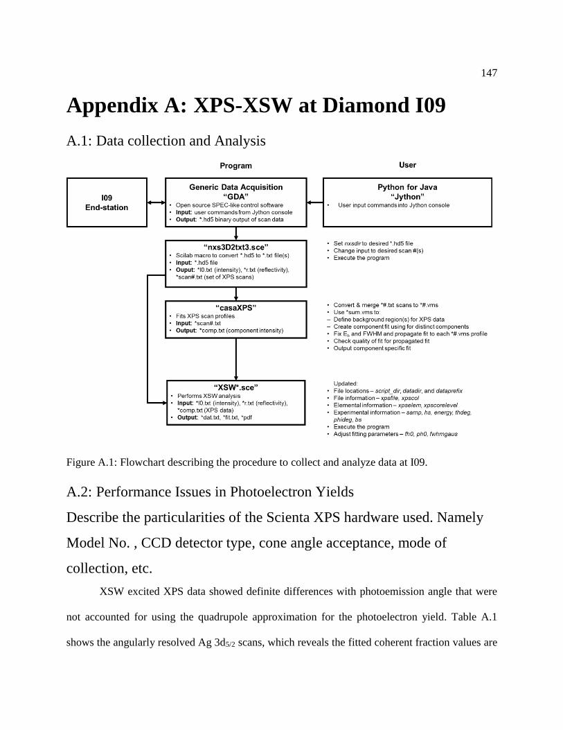
147
Appendix A: XPS-XSW at Diamond I09
A.1: Data collection and Analysis
Figure A.1: Flowchart describing the procedure to collect and analyze data at I09.
A.2: Performance Issues in Photoelectron Yields
Describe the particularities of the Scienta XPS hardware used. Namely
Model No. , CCD detector type, cone angle acceptance, mode of
collection, etc.
XSW excited XPS data showed definite differences with photoemission angle that were
not accounted for using the quadrupole approximation for the photoelectron yield. Table A.1
shows the angularly resolved Ag 3d5/2 scans, which reveals the fitted coherent fraction values are
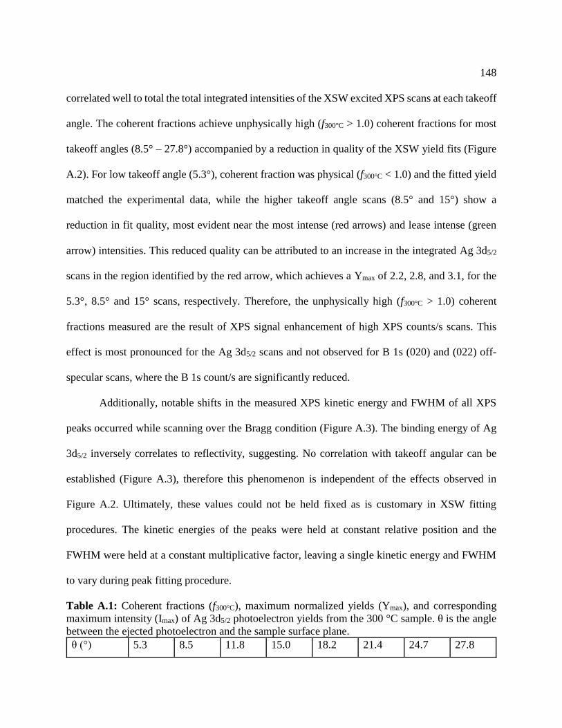
148
correlated well to total the total integrated intensities of the XSW excited XPS scans at each takeoff
angle. The coherent fractions achieve unphysically high (f300°C > 1.0) coherent fractions for most
takeoff angles (8.5° – 27.8°) accompanied by a reduction in quality of the XSW yield fits (Figure
A.2). For low takeoff angle (5.3°), coherent fraction was physical (f300°C < 1.0) and the fitted yield
matched the experimental data, while the higher takeoff angle scans (8.5° and 15°) show a
reduction in fit quality, most evident near the most intense (red arrows) and lease intense (green
arrow) intensities. This reduced quality can be attributed to an increase in the integrated Ag 3d5/2
scans in the region identified by the red arrow, which achieves a Ymax of 2.2, 2.8, and 3.1, for the
5.3°, 8.5° and 15° scans, respectively. Therefore, the unphysically high (f300°C > 1.0) coherent
fractions measured are the result of XPS signal enhancement of high XPS counts/s scans. This
effect is most pronounced for the Ag 3d5/2 scans and not observed for B 1s (020) and (022) off-
specular scans, where the B 1s count/s are significantly reduced.
Additionally, notable shifts in the measured XPS kinetic energy and FWHM of all XPS
peaks occurred while scanning over the Bragg condition (Figure A.3). The binding energy of Ag
3d5/2 inversely correlates to reflectivity, suggesting. No correlation with takeoff angular can be
established (Figure A.3), therefore this phenomenon is independent of the effects observed in
Figure A.2. Ultimately, these values could not be held fixed as is customary in XSW fitting
procedures. The kinetic energies of the peaks were held at constant relative position and the
FWHM were held at a constant multiplicative factor, leaving a single kinetic energy and FWHM
to vary during peak fitting procedure.
Table A.1: Coherent fractions (f300°C), maximum normalized yields (Ymax), and corresponding
maximum intensity (Imax) of Ag 3d5/2 photoelectron yields from the 300 °C sample. θ is the angle
between the ejected photoelectron and the sample surface plane.
θ (°) 5.3 8.5 11.8 15.0 18.2 21.4 24.7 27.8
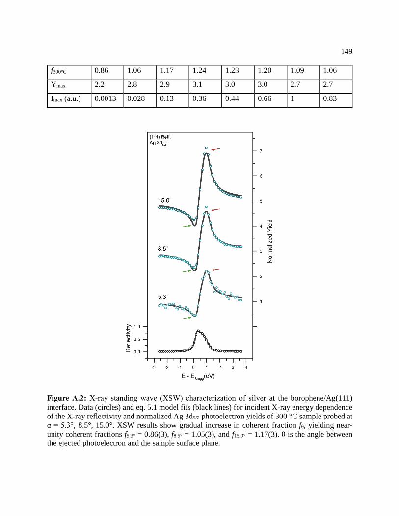
149
f300°C 0.86 1.06 1.17 1.24 1.23 1.20 1.09 1.06
Ymax 2.2 2.8 2.9 3.1 3.0 3.0 2.7 2.7
Imax (a.u.) 0.0013 0.028 0.13 0.36 0.44 0.66 1 0.83
Figure A.2: X-ray standing wave (XSW) characterization of silver at the borophene/Ag(111)
interface. Data (circles) and eq. 5.1 model fits (black lines) for incident X-ray energy dependence
of the X-ray reflectivity and normalized Ag 3d5/2 photoelectron yields of 300 °C sample probed at
α = 5.3°, 8.5°, 15.0°. XSW results show gradual increase in coherent fraction fθ, yielding near-
unity coherent fractions f5.3° = 0.86(3), f8.5° = 1.05(3), and f15.0° = 1.17(3). θ is the angle between
the ejected photoelectron and the sample surface plane.

150
Figure A.3: X-ray photoelectron spectroscopy fitting parameters of Ag 3d spectra during X-ray
standing wave characterization of the 300 °C sample probed at α = 5.3° and 15.0°.
0.4
0.45
0.5
0.55
0.6
0.65
0 10 20 30 40
FW
HM
(eV
)
Step
369.26
369.28
369.3
369.32
369.34
369.36
369.38
369.4
0 10 20 30 40
Bin
din
g E
nerg
y (
eV
)
Step
5.3°
15.0°
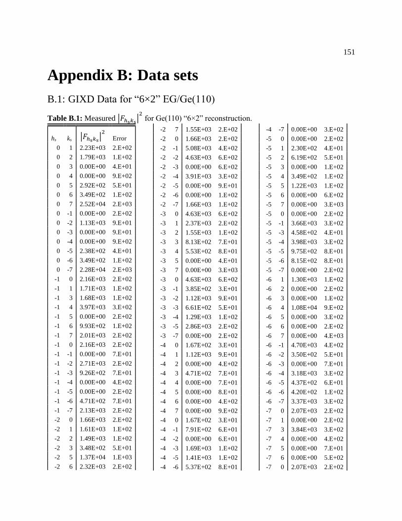
151
Appendix B: Data sets
B.1: GIXD Data for “6×2” EG/Ge(110)
Table B.1: Measured |𝐹ℎs𝑘s|
2 for Ge(110) “6×2” reconstruction.
hs ks |𝐹ℎs𝑘s|
2 Error
0 1 2.23E+03 2.E+02
0 2 1.79E+03 1.E+02
0 3 0.00E+00 4.E+01
0 4 0.00E+00 9.E+02
0 5 2.92E+02 5.E+01
0 6 3.49E+02 1.E+02
0 7 2.52E+04 2.E+03
0 -1 0.00E+00 2.E+02
0 -2 1.13E+03 9.E+01
0 -3 0.00E+00 9.E+01
0 -4 0.00E+00 9.E+02
0 -5 2.38E+02 4.E+01
0 -6 3.49E+02 1.E+02
0 -7 2.28E+04 2.E+03
-1 0 2.16E+03 2.E+02
-1 1 1.71E+03 1.E+02
-1 3 1.68E+03 1.E+02
-1 4 3.97E+03 3.E+02
-1 5 0.00E+00 2.E+02
-1 6 9.93E+02 1.E+02
-1 7 2.01E+03 2.E+02
-1 0 2.16E+03 2.E+02
-1 -1 0.00E+00 7.E+01
-1 -2 2.71E+03 2.E+02
-1 -3 9.26E+02 7.E+01
-1 -4 0.00E+00 4.E+02
-1 -5 0.00E+00 2.E+02
-1 -6 4.71E+02 7.E+01
-1 -7 2.13E+03 2.E+02
-2 0 1.66E+03 2.E+02
-2 1 1.61E+03 1.E+02
-2 2 1.49E+03 1.E+02
-2 3 3.48E+02 5.E+01
-2 5 1.37E+04 1.E+03
-2 6 2.32E+03 2.E+02
-2 7 1.55E+03 2.E+02
-2 0 1.66E+03 2.E+02
-2 -1 5.08E+03 4.E+02
-2 -2 4.63E+03 6.E+02
-2 -3 0.00E+00 6.E+02
-2 -4 3.91E+03 3.E+02
-2 -5 0.00E+00 9.E+01
-2 -6 0.00E+00 1.E+02
-2 -7 1.66E+03 1.E+02
-3 0 4.63E+03 6.E+02
-3 1 2.37E+03 2.E+02
-3 2 1.55E+03 1.E+02
-3 3 8.13E+02 7.E+01
-3 4 5.53E+02 8.E+01
-3 5 0.00E+00 4.E+01
-3 7 0.00E+00 3.E+03
-3 0 4.63E+03 6.E+02
-3 -1 3.85E+02 3.E+01
-3 -2 1.12E+03 9.E+01
-3 -3 6.61E+02 5.E+01
-3 -4 1.29E+03 1.E+02
-3 -5 2.86E+03 2.E+02
-3 -7 0.00E+00 2.E+02
-4 0 1.67E+02 3.E+01
-4 1 1.12E+03 9.E+01
-4 2 0.00E+00 4.E+02
-4 3 4.71E+02 7.E+01
-4 4 0.00E+00 7.E+01
-4 5 0.00E+00 8.E+01
-4 6 0.00E+00 4.E+02
-4 7 0.00E+00 9.E+02
-4 0 1.67E+02 3.E+01
-4 -1 7.91E+02 6.E+01
-4 -2 0.00E+00 6.E+01
-4 -3 1.69E+03 1.E+02
-4 -5 1.41E+03 1.E+02
-4 -6 5.37E+02 8.E+01
-4 -7 0.00E+00 3.E+02
-5 0 0.00E+00 2.E+02
-5 1 2.30E+02 4.E+01
-5 2 6.19E+02 5.E+01
-5 3 0.00E+00 1.E+02
-5 4 3.49E+02 1.E+02
-5 5 1.22E+03 1.E+02
-5 6 0.00E+00 6.E+02
-5 7 0.00E+00 3.E+03
-5 0 0.00E+00 2.E+02
-5 -1 3.66E+03 3.E+02
-5 -3 4.58E+02 4.E+01
-5 -4 3.98E+03 3.E+02
-5 -5 9.75E+02 8.E+01
-5 -6 8.15E+02 8.E+01
-5 -7 0.00E+00 2.E+02
-6 1 1.30E+03 1.E+02
-6 2 0.00E+00 2.E+02
-6 3 0.00E+00 1.E+02
-6 4 1.08E+04 9.E+02
-6 5 0.00E+00 3.E+02
-6 6 0.00E+00 2.E+02
-6 7 0.00E+00 4.E+03
-6 -1 4.70E+03 4.E+02
-6 -2 3.50E+02 5.E+01
-6 -3 0.00E+00 7.E+01
-6 -4 3.18E+03 3.E+02
-6 -5 4.37E+02 6.E+01
-6 -6 4.20E+02 1.E+02
-6 -7 3.37E+03 3.E+02
-7 0 2.07E+03 2.E+02
-7 1 0.00E+00 2.E+02
-7 3 3.84E+03 3.E+02
-7 4 0.00E+00 4.E+02
-7 5 0.00E+00 7.E+01
-7 6 0.00E+00 5.E+02
-7 0 2.07E+03 2.E+02
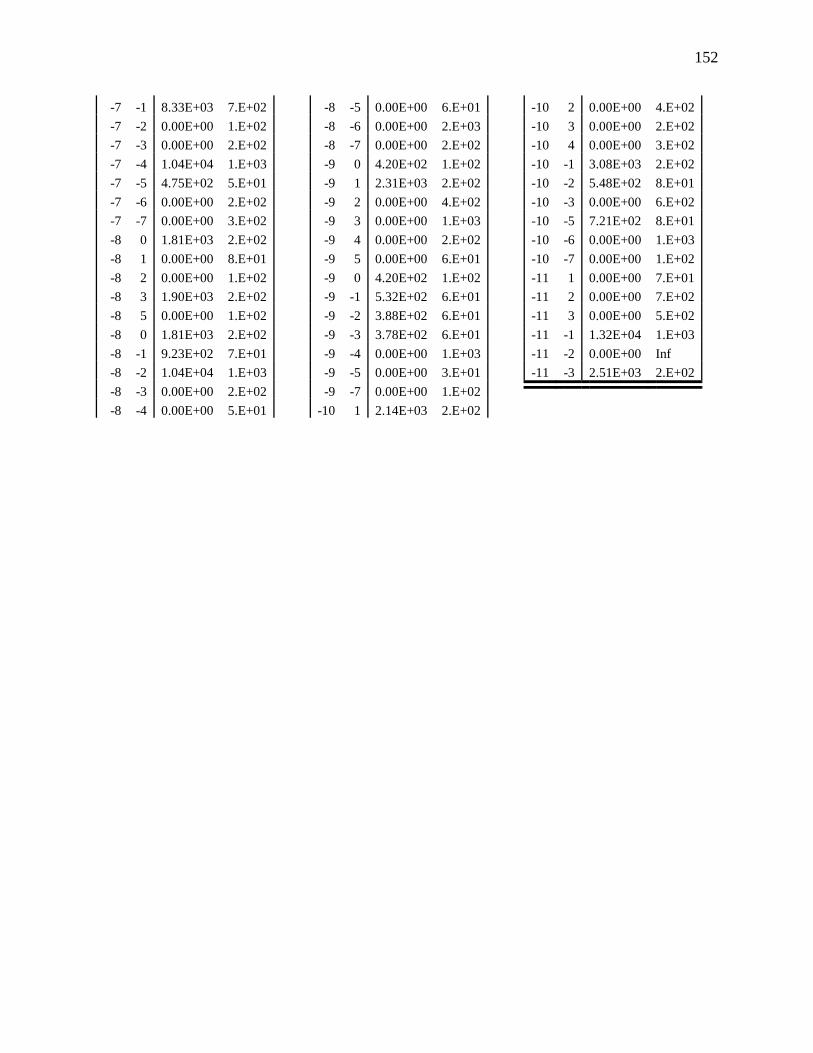
152
-7 -1 8.33E+03 7.E+02
-7 -2 0.00E+00 1.E+02
-7 -3 0.00E+00 2.E+02
-7 -4 1.04E+04 1.E+03
-7 -5 4.75E+02 5.E+01
-7 -6 0.00E+00 2.E+02
-7 -7 0.00E+00 3.E+02
-8 0 1.81E+03 2.E+02
-8 1 0.00E+00 8.E+01
-8 2 0.00E+00 1.E+02
-8 3 1.90E+03 2.E+02
-8 5 0.00E+00 1.E+02
-8 0 1.81E+03 2.E+02
-8 -1 9.23E+02 7.E+01
-8 -2 1.04E+04 1.E+03
-8 -3 0.00E+00 2.E+02
-8 -4 0.00E+00 5.E+01
-8 -5 0.00E+00 6.E+01
-8 -6 0.00E+00 2.E+03
-8 -7 0.00E+00 2.E+02
-9 0 4.20E+02 1.E+02
-9 1 2.31E+03 2.E+02
-9 2 0.00E+00 4.E+02
-9 3 0.00E+00 1.E+03
-9 4 0.00E+00 2.E+02
-9 5 0.00E+00 6.E+01
-9 0 4.20E+02 1.E+02
-9 -1 5.32E+02 6.E+01
-9 -2 3.88E+02 6.E+01
-9 -3 3.78E+02 6.E+01
-9 -4 0.00E+00 1.E+03
-9 -5 0.00E+00 3.E+01
-9 -7 0.00E+00 1.E+02
-10 1 2.14E+03 2.E+02
-10 2 0.00E+00 4.E+02
-10 3 0.00E+00 2.E+02
-10 4 0.00E+00 3.E+02
-10 -1 3.08E+03 2.E+02
-10 -2 5.48E+02 8.E+01
-10 -3 0.00E+00 6.E+02
-10 -5 7.21E+02 8.E+01
-10 -6 0.00E+00 1.E+03
-10 -7 0.00E+00 1.E+02
-11 1 0.00E+00 7.E+01
-11 2 0.00E+00 7.E+02
-11 3 0.00E+00 5.E+02
-11 -1 1.32E+04 1.E+03
-11 -2 0.00E+00 Inf
-11 -3 2.51E+03 2.E+02