
New I2C driver - tesla.zabotavdome.rutesla.zabotavdome.ru/pic/books/LinuxI2CDriver.pdf · The new...
25
New I2C driver ~ Oscilloscope pictures of I2C transactions Geert Vancompernolle 1. Setup of the new driver The new I2C driver setup has 3 extra functions, accessible via IOCTL (for high level I2C access from user space) or directly (for driver access in kernel space). The 3 extra functions are: 1. void i2c_read( unsigned char slave, unsigned char* rbuf, unsigned char rlen ); When called, this function will read a certain amount of bytes (limited to 256) from the device addressed into a read buffer allocated by the caller. 2. void i2c_write( unsigned char slave, unsigned char* wbuf, unsigned char wlen ); When called, this function will write a certain amount of bytes (limited to 256) from a write buffer to the device addressed. 3. void i2c_writeread( unsigned char slave , unsigned char* wbuf , unsigned char wlen , unsigned char* rbuf , unsigned char rlen ); When called, this function will read a certain amount of bytes (limited to 256) from a specified address previously set by writing the address to the device prior to reading from the device. To be able to use those functions, the following I2C data structure has been defined: typedef struct _I2C_DATA { unsigned char slave; /* I2C address (8-bit representation) of slave device */ unsigned char wbuf[256]; /* Write buffer (length = 256 bytes) */ unsigned int wlen; /* Number of bytes to write from wbuf[] */ unsigned char rbuf[256]; /* Read buffer (length = 256 bytes) */ unsigned int rlen; /* Number of bytes to read into rbuf[] */ } I2C_DATA; The first item contains the address of the slave The second item is the write buffer where the caller can store the data to be sent to the slave The third item is the number of bytes in the write buffer to send to the slave (limited to 256) The fourth item is the read buffer where the caller can store the data received by the slave The fifth item is the number of bytes to receive from the slave (limited to 256)
Transcript of New I2C driver - tesla.zabotavdome.rutesla.zabotavdome.ru/pic/books/LinuxI2CDriver.pdf · The new...
New I2C driver
~
Oscilloscope pictures of I2C transactions Geert Vancompernolle
1. Setup of the new driver The new I2C driver setup has 3 extra functions, accessible via IOCTL (for high level I2C access from user space) or directly (for driver access in kernel space). The 3 extra functions are:
1. void i2c_read( unsigned char slave, unsigned char* rbuf, unsigned char rlen ); When called, this function will read a certain amount of bytes (limited to 256) from the device addressed into a read buffer allocated by the caller.
2. void i2c_write( unsigned char slave, unsigned char* wbuf, unsigned char wlen ); When called, this function will write a certain amount of bytes (limited to 256) from a write buffer to the device addressed.
3. void i2c_writeread( unsigned char slave , unsigned char* wbuf , unsigned char wlen , unsigned char* rbuf , unsigned char rlen ); When called, this function will read a certain amount of bytes (limited to 256) from a specified address previously set by writing the address to the device prior to reading from the device.
To be able to use those functions, the following I2C data structure has been defined: typedef struct _I2C_DATA { unsigned char slave; /* I2C address (8-bit representation) of slave device */ unsigned char wbuf[256]; /* Write buffer (length = 256 bytes) */ unsigned int wlen; /* Number of bytes to write from wbuf[] */ unsigned char rbuf[256]; /* Read buffer (length = 256 bytes) */ unsigned int rlen; /* Number of bytes to read into rbuf[] */ } I2C_DATA; The first item contains the address of the slave The second item is the write buffer where the caller can store the data to be sent to the slave The third item is the number of bytes in the write buffer to send to the slave (limited to 256) The fourth item is the read buffer where the caller can store the data received by the slave The fifth item is the number of bytes to receive from the slave (limited to 256)

The above defined functions use this data structure in different ways.
1. Read To read from the device, you only need to specify the slave address, the read buffer and the number of bytes to read from the slave. The other parameters are left unchanged by this function.
2. Write To write to the device, you only need to specify the slave address, the write buffer and the number of bytes to write to the slave. The other parameters are left unchanged by this function.
3. Write/Read. This is a special function, which must be used when you want to write the address to the slave, where you want to read from. Devices using this protocol are, for instance, EEPROM’s (such as the 24C32 NVM from ST). In this special case, all 5 data structure elements are used. The slave address is obvious. Then, the write buffer contains the address to be written to the slave, from which you want to read from. Also specify the amount of bytes to write to the slave… Finally, the read buffer will contain the data read from the slave. Also here, you must specify the amount of bytes that will be read from the slave.
The corresponding IOCTL calls are: a. Read ioctl( fd_i2c, _IO( ETRAXI2C_IOCTYPE, I2C_READ ) , &<I2C datastruct> ) ) b. Write ioctl( fd_i2c, _IO( ETRAXI2C_IOCTYPE, I2C_WRITE ) , &<I2C datastruct>) ) c. WriteRead ioctl( fd_i2c, _IO( ETRAXI2C_IOCTYPE, I2C_WRITEREAD ) , &<I2C datastruct>) ) Preparation of the I2C data buffer. In the pseudo-example below, we want to write and read from an NVM device of type 24C32 (8kB EEPROM) with slave address 0xA0. We want to write the value 0x75 on address location 0x0000 and then we want to read it back.
I2CDATA examplebuf; examplebuf.slave = 0xA0; examplebuf.wbuf[ 0 ] = 0; examplebuf.wbuf[ 1 ] = 0; examplebuf.wbuf[ 2 ] = 0x75; examplebuf.wlen = 3; examplebuf.rlen = 1;
Commands:
ioctl( fd_i2c, _IO( ETRAXI2C_IOCTYPE, I2C_WRITE ), &examplebuf ); wait_10ms; ioctl( fd_i2c, _IO( ETRAXI2C_IOCTYPE, I2C_WRITEREAD ), &examplebuf );

Return values of the IOCTL call. I’ve introduced new error numbers, typically dedicated to I2C communication. The error numbers are stored in a file called i2c_errno.h, which is located in /include/asm-cris. The following error values are defined: #define EI2CNOERRORS 0 /* All fine */ #define EI2CBUSNFREE 1 /* I2C bus not free */ #define EI2CWADDRESS 2 /* Address write failed */ #define EI2CRADDRESS 3 /* Address read failed */ #define EI2CSENDDATA 4 /* Sending data failed */ #define EI2CRECVDATA 5 /* Receiving data failed */ #define EI2CSTRTCOND 6 /* Start condition failed */ #define EI2CRSTACOND 7 /* Repeated start condition failed */ #define EI2CSTOPCOND 8 /* Stop condition failed */ #define EI2CNOSNDBYT 9 /* Number of send bytes is 0, while there's a send buffer defined */ #define EI2CNOSNDBUF 10 /* No send buffer defined, while number of send bytes is not 0 */ #define EI2CNORCVBYT 11 /* Number of receive bytes is 0, while there's a receive buffer defined */ #define EI2CNORCVBUF 12 /* No receive buffer defined, while number of receive bytes is not 0 */ #define EI2CNOACKNLD 13 /* No acknowledge received from slave */ #define EI2CNOMNUMBR 14 /* No MAJOR number received from kernel while registering the device */
The header file i2c_errno.h is nowhere included, apart from the application where you want to use it. The only consequence of adding error numbers returned from the I2C functions is that the return type of some I2C functions defined in i2c.h should not be void anymore, but int. This is the new content for i2c.h: /* $Id: i2c.h,v 1.3 2004/05/28 09:26:59 starvik Exp $ */ #ifndef _I2C_H #define _I2C_H int i2c_init(void); /* High level I2C actions */ int i2c_writereg(unsigned char theSlave, unsigned char theReg, unsigned char theValue); unsigned char i2c_readreg(unsigned char theSlave, unsigned char theReg); /* Low level I2C */ int i2c_start(void); int i2c_stop(void); int i2c_outbyte(unsigned char x); unsigned char i2c_inbyte(void); int i2c_getack(void); void i2c_sendack(void); void i2c_sendnack(void); /**GVC**/ /* New low level I2C functions */ int i2c_read( unsigned char slave, unsigned char* rbuf, unsigned char rlen ); int i2c_write( unsigned char slave, unsigned char* wbuf, unsigned char wlen ); int i2c_writeread( unsigned char slave , unsigned char* wbuf , unsigned char wlen , unsigned char* rbuf , unsigned char rlen ); /**END GVC**/ #endif /* _I2C_H */
Since previous return types were void, no one used them in other code, so to me it will not break old code…

1.1 Writing to a NVM (EEPROM) device This section describes writing to a NVM device of type 24C32 (8kB of electrical erasable memory). To write to a NVM, one has to set the address where he wants to write first. The address takes up 2 bytes (see NVM spec). The last byte in the sequence is the value you want to write to that address. So, the transfer protocol is:
STA – SLA_ADDR – ADDR_BYTE1 – ADDR_BYTE2 – VALUE – STOP Below, you can find screen shots of the I2C communication. 1. Complete write sequence
This picture shows the write sequence to the NVM. First, the address 0xA0 is sent on the bus and is ACK’ed by the device. Next, two address bytes (here, twice 0x00) are sent to the NVM, each of them ACK’ed too. Finally, the value for address 0x0000 is sent (here, 00000111b) and is followed by an ACK from the NVM. Below, you can find more detailed views of the complete write sequence: a. The slave “write” address (0xA0) and the first address byte (0x00).
See how the ACK pulses are improved compared to the previous version of the driver (v1.0) There are no obsolete ups and downs anymore on the SDA line when generating the ACK pulse.

b. The ACK of the 1st address byte, the complete 2nd address byte and the value written to address 0xA0 (here, 00011000b).
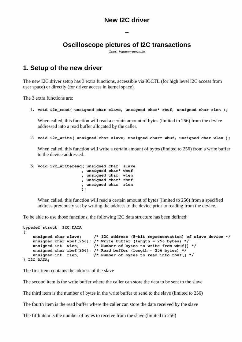
2. Detail of the start condition
In the above picture, a detailed view is given of the start condition (start condition is the moment SCL goes low when SDA is already low). You clearly see the delta of 4us between the falling edge of the SDA (red line) and the falling edge of the SCL (blue line). This is according the I2C standard. 3. Measurement of the SCL speed
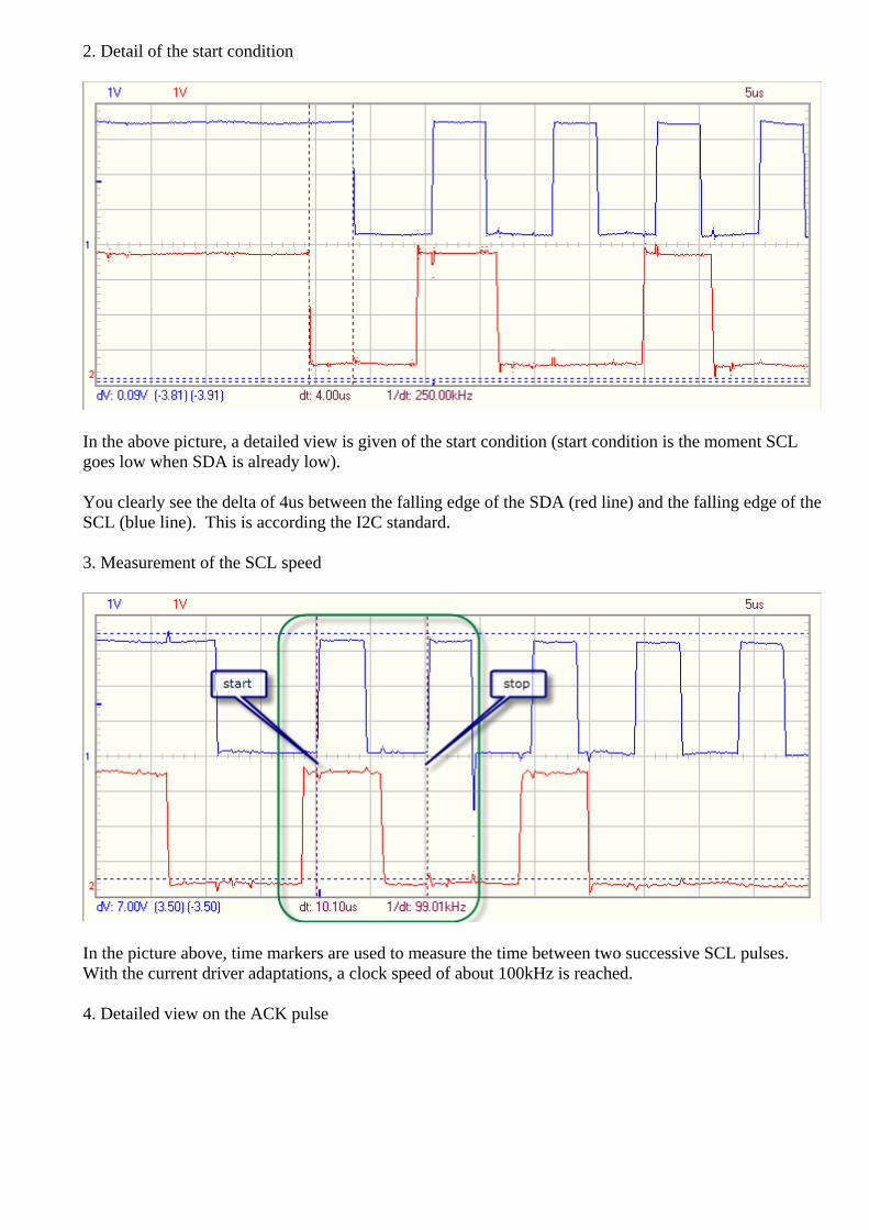
In the picture above, time markers are used to measure the time between two successive SCL pulses. With the current driver adaptations, a clock speed of about 100kHz is reached. 4. Detailed view on the ACK pulse

In the picture above, the ACK of the slave is clearly visible. In the previous version of the driver (v1.0), there was a short “HIGH” just before the SDA line was pulled low by the slave. Once the slave released the SDA line, the master was pulling the line high again. This could have a very nasty side effect: in some special occasions, this was seen as a STA condition for some components in the circuitry. The current implementation got rid of the “spikes” on the SDA line, resulting in a much more correct behaviour of the whole system during ACK/NAC. 5. Detailed view on writing the value to the NVM
In the picture above, you see three different stages in the I2C communication. The first one, indicated by an orange line, is the last ACK of the 2nd address byte sent to the NVM. Next, the data to be written is given (here, 0xFE). The slave confirms it has received the value by sending an ACK (blue line). Once the master sees this, it generates a STOP condition (green line). The time markers indicate a delay of 4us between SCL high and SDA high (as specified for the I2C protocol).

1.2 Reading from an NVM device This section describes reading from a NVM device of type 24C32 (8kB of electrical erasable memory). To read from a NVM, one has to set the address where he wants to read from first. The address takes up 2 bytes (see NVM spec). Then, there must be a repeated start condition to start the reading process. So, the transfer protocol is: STA – SLA_ADDR – ADDR_BYTE1 – ADDR_BYTE2 – RSTA – SLA_ADDR – VALUE1 –
VALUE2 - … - VALUE_N – STOP Below, you can find screen shots of the I2C communication. 1. Complete view of the Write/Read I2C transaction.
The above picture shows you the complete write/read cycle. First, the address is written where you want to read from (address 0x00), followed by a repeated start condition to read the value at location 0x00. 2. Write/Read: part 1

The above picture shows a bit more in detail the slave address and the first of the two address bytes written, each with their respective ACK pulse. 3. Write/Read: part 2
In the above picture, you see the second part of the address byte to be written to the NVM. Next, the repeated STA condition is shown (see further for a detailed view) and then again the slave address of the device, but this time the READ bit is set. 4. Write/Read: part 3
In the above picture, you see 3 important stages in the read section of the Write/Read transaction.
1. The 1st highlight rectangle. This indicates the repeated start generation. First, the SDA line is pulled high, almost immediately followed by the SCL line that’s pulled high too. Shortly after the SDA line is pulled low again. This realises the REPEATED START condition (there was no STOP condition before…). See details below:

2. The 2nd highlight rectangle. This indicates the last bit of the slave address being ‘1’. That means a READ action is to be executed. The READ bit is followed by an ACK of the slave. See details below:
3. The 3rd highlight rectangle. This indicates a NACK of the master. Since the master only wants to read one byte, it triggers the slave not to send any more bytes, by not acknowledging the byte just received. This is the only way the slave knows it doesn’t have to send any more bytes to the master. See details below.

IMPORTANT: All screen shots below are still valid, but they have now the “nice” ACK/NACK pulses (see all pictures above). There’s no unnecessary up/down visible anymore during ACK/NACK communication. I didn’t retake the screen shots due to lack of time…
1.3 Writing to a PCF8574 device The PCF8574 is an I2C controlled I/O-expander with 8 pins, each individually programmable as input or output. This is an easier I2C device, since you can only read or write to or from one location. 1. Writing to the device
The above picture shows the write sequence to the device (device address: 0x40).

After the slave has been addressed, it acknowledges and then the master sends the data to the device (here: 0xFA). Since the master only wants to send 1 byte, it generates a stop condition. In fact, the master can send as many bytes to the slave as he wants, as long as there’s no STOP condition generated. 2. Reading from the device. In the example below, 2 bytes are read from the PCF8574. Both have the same value, though… Part 1
The above picture shows the first part of the read action. The slave address is sent (mind the 8th bit, which is set to ‘1’). After the ACK, the slave sends the first byte. This byte is followed by an ACK, generated by the master. This way, the master indicates the slave it has received correctly the value from the slave and the slave immediately sends a new value on the bus, since the master has ACK’ed the byte received from the slave. Part 2
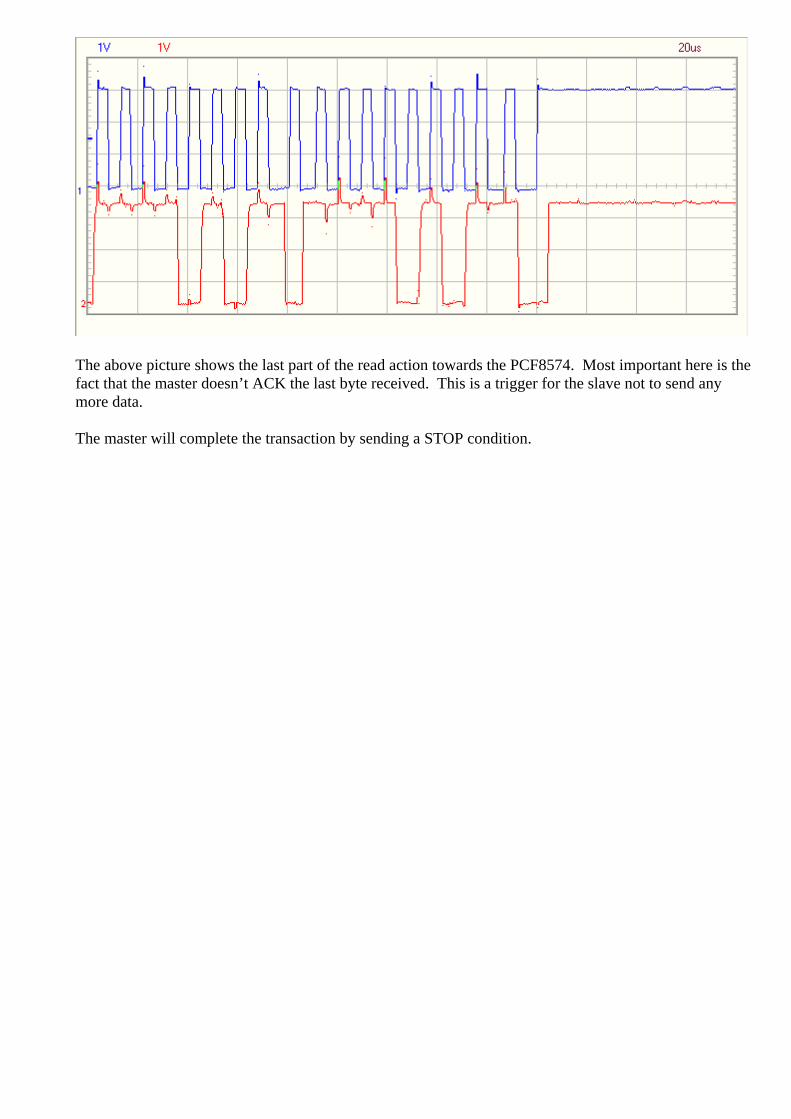
The above picture shows the last part of the read action towards the PCF8574. Most important here is the fact that the master doesn’t ACK the last byte received. This is a trigger for the slave not to send any more data. The master will complete the transaction by sending a STOP condition.
2. Some screen shots of the latest version of the I2C driver which is using the new return codes for I2C errors.
2.1 NVM (slave address: 0xA0)
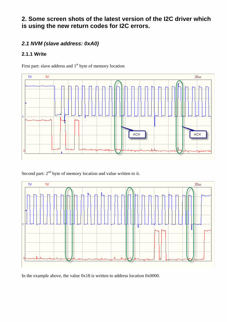
2.1.1 Write First part: slave address and 1st byte of memory location
Second part: 2nd byte of memory location and value written to it.
In the example above, the value 0x18 is written to address location 0x0000.
2.1.2. Read
2.2 PCF8574 (slave address: 0x40)
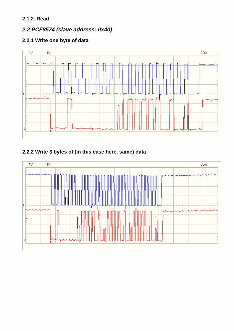
2.2.1 Write one byte of data
2.2.2 Write 3 bytes of (in this case here, same) data
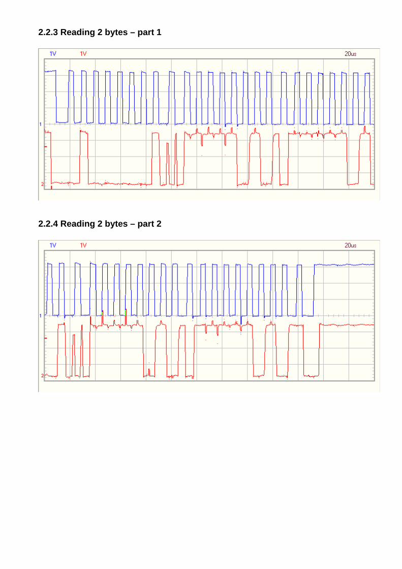
2.2.3 Reading 2 bytes – part 1
2.2.4 Reading 2 bytes – part 2

2.3 PCF8591 (address: 0x90)
2.3.1 Writing to the device Selecting channel AIN0 (control byte = 0x40).
Selecting channel AIN1 (control byte = 0x41).
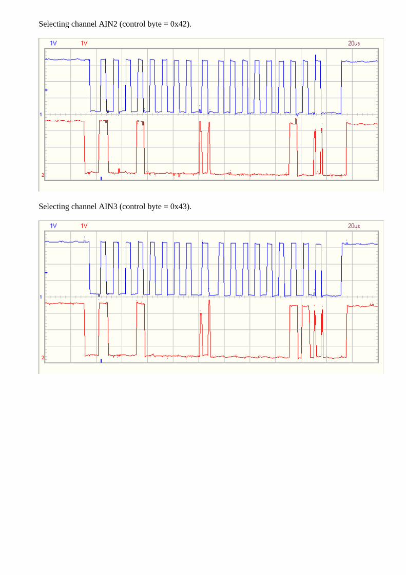
Selecting channel AIN2 (control byte = 0x42).
Selecting channel AIN3 (control byte = 0x43).

2.3.2 Reading ADC value from AIN0 When Vin of AINx changes, then the first byte read will still contain the previous conversion value. Because of this, you must always read two bytes from the device and only take the second byte into account. Only this byte contains the latest value. 1. Vin of AIN0 = 3.3V (= Vcc): part 1 = slave address + 1st byte read (ignored)
2. Vin of AIN0 = 3.3V (= Vcc): part 2 = 2nd byte read (ignored)
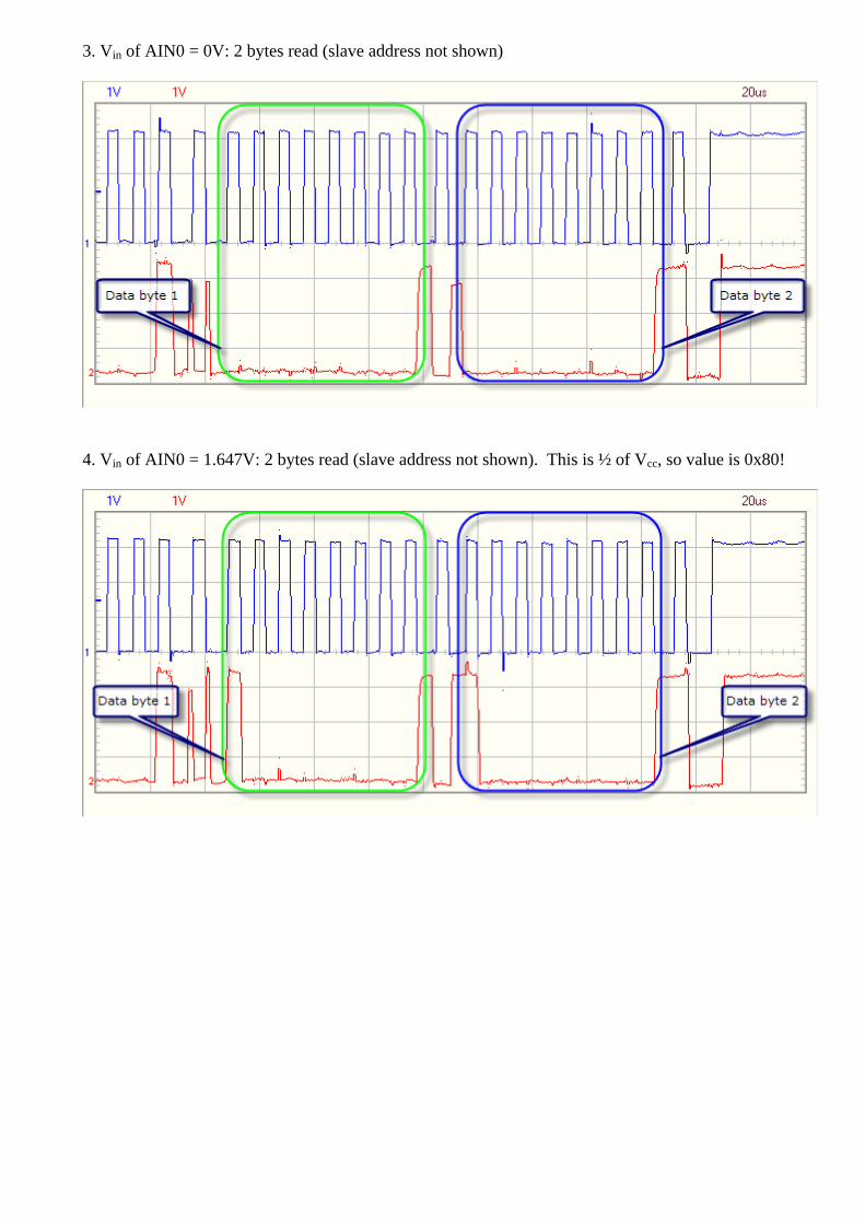
3. Vin of AIN0 = 0V: 2 bytes read (slave address not shown)
4. Vin of AIN0 = 1.647V: 2 bytes read (slave address not shown). This is ½ of Vcc, so value is 0x80!

December 2006Geert Vancompernolle

(1)
(1) Should normally be 5 us in stead of 4 us, but since the next action is setting the data line high or low, this is done 1 us before the clock is set high.This way, we fulfill the requirement of having 5 us between the falling edge of the previous clock pulse and the rising edge of the next one.
STARTCONDITION
SDA
SCL
STOPCONDITION
SDA
SCL
SEND BIT
SDA (0/1)
SCL
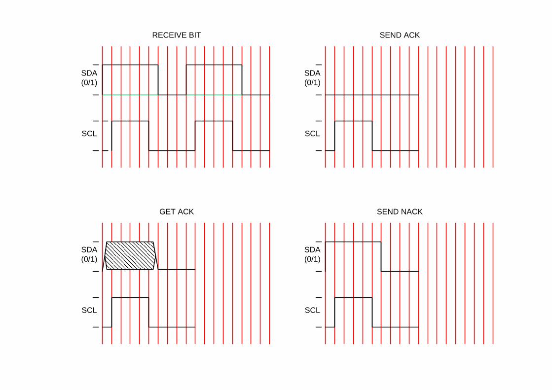
RECEIVE BIT
SDA (0/1)
SCL
SEND ACK
SDA (0/1)
SCL
GET ACK
SDA (0/1)
SCL
SEND NACK
SDA (0/1)
SCL
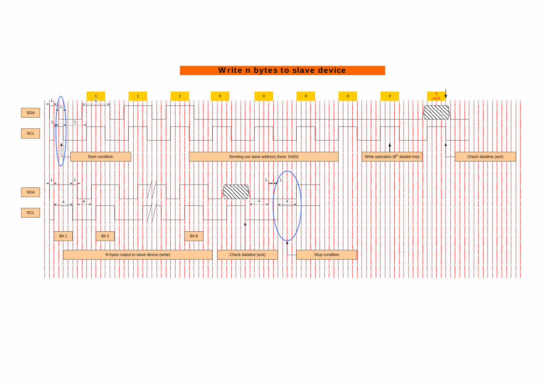
1 1 1 0 0 0 0 0 0ACK
Check dataline (ack)
Sending out slave address (here: 0xE0)Start condition
SDA
SCL
Check dataline (ack)
N bytes output to slave device (write)
Write operation (8th databit low)
Stop condition
Bit 1 Bit 2 Bit 8
SDA
SCL
4
1 1
4
11
11
5
11
44
Write n bytes to slave device
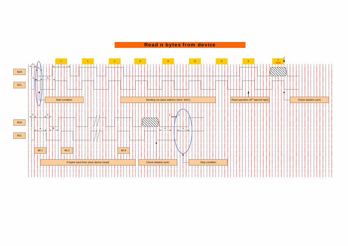
1 1 1 0 0 0 0 0 0ACK
Check dataline (ack)
Sending out slave address (here: 0xE1)Start condition
SDA
SCL
Check dataline (ack)
N bytes input from slave device (read)
Read operation (8th data bit high)
Stop condition
Bit 1 Bit 2 Bit 8
SDA
SCL
4
1 1
4
11
11
5
11
44
Read n bytes from device


