Neuron® 5000 Processor Data Sheet - Echelon...
7
1 Neuron ® 5000 Processor The Next-generation Neuron Chip for LONWORKS ® Control Networks Combined with inexpensive serial memory, the Neuron 5000 Processor provides a lower-cost, higher-performance L ON WORKS solution than those based on previous-generation Neuron 3120 ® and Neuron 3150 ® chips. The Neuron 5000 Processor incorporates communication and control functions on a single chip, in both hardware and firmware, to facilitate the design of a LONWORKS device. Its flexible 5-pin communications port can be configured to interface with a wide variety of media transceivers — including twisted-pair, RF, IR, fiber-optics, and coaxial — at a wide range of data rates. • 3.3V operation. • Higher-performance Neuron ® Core — internal system clock scales up to 80 MHz. • Enables lower-cost device designs. • Serial memory interface for inexpensive external EEPROM and flash non-volatile memories. • Supports up to 254 Network Variables (NVs) and 127 aliases. • User programmable interrupts provide faster response time to external events. • Includes hardware UART with 16-byte receive and transmit FIFOs. • 7mm x 7mm 48-pin QFN package. • 5-pin network communications port with 3.3V drive and 5V-tolerant pins. • 12 I/O pins with 35 programmable standard I/O models. • Supports up to 42KB of application code space. • 64KB RAM (44KB user accessible) and 16KB ROM on-chip memories. • Unique 48-bit Neuron ID in every device for network installation and management. • -40°C to +85°C operating temperature range. The Neuron 5000 Processor includes 3 independent 8-bit logical processors to manage the physical MAC layer, the network, and the user application. These are called the Media-Access Control (MAC) processor, the network (NET) processor, and the application (APP) processor, respectively (see Figure 1). At higher system clock rates, there is also a fourth processor to handle interrupts. I / O Comm Port External Transformer JTAG 5 XIN XOUT RST~ SVC~ Clock, Reset, and Service IRQ CPU APP CPU NET CPU MAC CPU Serial Memory Interface NVM (SPI or I 2 C) ROM (16K x 8) RAM (64K x 8) / / 12 2-6 5 / Figure 1: Neuron 5000 Processor Backward Compatibility The pins for the Neuron 5000 Processor’s communications port drive a 3.3V signal and are 5V input-tolerant. Thus, the Neuron 5000 Processor is compatible with 3.3V transceivers and with 5V transceivers that have TTL- compatible input. The Neuron 5000 Processor is compatible with TP/XF-1250 and EIA- 485 channels, and can be used with the LONWORKS LPT-11 Link Power Transceiver. It also supports a variety of other channels used with previous-generation Neuron Chips, such as RF, IR, fiber-optic, and coaxial. It does not, however, support a TP/XF-78 channel. To support a TP/FT- 10 channel, use an Echelon Free Topology Smart Transceiver (FT 5000 Smart Transceiver); to support a PL-20 power line channel, use an Echelon Power Line Smart Transceiver (PL 3120/3150/3170 Smart Transceiver). Echelon’s Smart Transceivers integrate the transceiver for the channel type and the Neuron Core into a single chip, which enables smaller designs and provides cost savings. The Neuron Core in the Neuron 5000 Processor uses the same instruction set and architecture as the previous- generation Neuron Core, with 2 new additional instructions for hardware FEATURES DESCRIPTION
Transcript of Neuron® 5000 Processor Data Sheet - Echelon...

1
Neuron® 5000 Processor
The Next-generation Neuron Chip for LONWORKS® Control Networks
Combined with inexpensive serial memory, the Neuron 5000 Processor provides a lower-cost, higher-performance LONWORKS solution than those based on previous-generation Neuron 3120® and Neuron 3150® chips.The Neuron 5000 Processor incorporates communication and control functions on a single chip, in both hardware and firmware, to facilitate the design of a LONWORKS device. Its flexible 5-pin communications port can be configured to interface with a wide variety of media transceivers— including twisted-pair, RF, IR, fiber-optics, and coaxial—at a wide range of data rates.
• 3.3V operation.• Higher-performance Neuron® Core —
internal system clock scales up to 80 MHz.
• Enables lower-cost device designs.• Serial memory interface for
inexpensive external EEPROM and flash non-volatile memories.
• Supports up to 254 Network Variables (NVs) and 127 aliases.
• User programmable interrupts provide faster response time to external events.
• Includes hardware UART with 16-byte receive and transmit FIFOs.
• 7mm x 7mm 48-pin QFN package.• 5-pin network communications port
with 3.3V drive and 5V-tolerant pins.• 12 I/O pins with 35 programmable
standard I/O models.• Supports up to 42KB of application
code space.• 64KB RAM (44KB user accessible)
and 16KB ROM on-chip memories.• Unique 48-bit Neuron ID in every
device for network installation and management.
• -40°C to +85°C operating temperature range.
The Neuron 5000 Processor includes 3 independent 8-bit logical processors to manage the physical MAC layer, the network, and the user application. These are called the Media-Access Control (MAC) processor, the network (NET) processor, and the application (APP) processor, respectively (see Figure 1). At higher system clock rates, there is also a fourth processor to handle interrupts.
I / O CommPort
ExternalTransformer
JTAG
5
XIN
XOU
T
RST
~
SVC
~
Clock, Reset,and Service
IRQ CPU
APP CPU
NET CPU
MAC CPU
SerialMemoryInterface
NVM(SPI or I2C)
ROM(16K x 8)
RAM(64K x 8)
/
/12
2-6
5/
Figure 1: Neuron 5000 Processor
Backward CompatibilityThe pins for the Neuron 5000 Processor’s communications port drive a 3.3V signal and are 5V input-tolerant. Thus, the Neuron 5000 Processor is compatible with 3.3V transceivers and with 5V transceivers that have TTL-compatible input.
The Neuron 5000 Processor is compatible with TP/XF-1250 and EIA-485 channels, and can be used with the LonWorks LPT-11 Link Power Transceiver. It also supports a variety of other channels used with previous-generation Neuron Chips, such as RF, IR, fiber-optic, and coaxial. It does not, however, support a TP/XF-78 channel. To support a TP/FT-10 channel, use an Echelon Free Topology Smart Transceiver (FT 5000 Smart Transceiver); to support a PL-20 power line channel, use an Echelon Power Line Smart Transceiver (PL 3120/3150/3170 Smart Transceiver). Echelon’s Smart Transceivers integrate the transceiver for the channel type and the Neuron Core into a single chip, which enables smaller designs and provides cost savings.
The Neuron Core in the Neuron 5000 Processor uses the same instruction set and architecture as the previous-generation Neuron Core, with 2 new additional instructions for hardware
FEATURES DESCRIPTION
2
multiplication and division. The Series 5000 Neuron Core is source code compatible with applications written for the Series 3100 Neuron Core. Applications written for the Series 3100 Neuron Core must be recompiled with the NodeBuilder® FX Development Tool or the Mini FX Evaluation Kit before they can be used with the Neuron 5000 Processor.
The Neuron 5000 Processor uses Neuron firmware version 19. Firmware versions prior to version 19 are not compatible with the Neuron 5000 Processor. The Neuron firmware is pre-programmed into the on-chip ROM. The Neuron 5000 Processor can also be configured to read newer firmware from external memories, allowing the firmware to be upgraded over time.
Enhanced PerformanceFaster system clock. The internal system clock for the Neuron 5000 Processor can be user-configured to run from 5MHz to 80MHz. The required external crystal provides a 10MHz clock frequency, and an internal PLL boosts the frequency to a maximum of 80MHz as the internal system clock speed. The previous-generation Neuron 3120/3150 Core divided the external oscillator frequency by two to create the internal system clock. Hence, a Neuron 3120/3150 Core running with a 10MHz external crystal had a 5MHz internal system clock. A Neuron 5000 Processor running with an 80MHz internal clock is thus 16 times faster than a 10MHz Neuron 3120/3150 Core running with a 5MHz internal system clock.
The 5MHz system clock mode in the Neuron 5000 Processor provides backward compatibility to support time-critical applications designed for the 10MHz Neuron 3150 or Neuron 3120 processor.
The Neuron Core inside the Neuron 5000 Processor includes a built-in hardware multiplier and divider to increase the performance of arithmetic operations.
Support for more network variables. Because it uses Neuron system firmware Version 19, the Neuron 5000 Processor supports applications with up to 254 network variables and 127 aliases for Neuron hosted devices (devices without a host microprocessor). A Series 3100 Neuron Chip or Smart Transceiver with Neuron firmware Version 15 or earlier supports up to 62 network variables and 62 aliases for Neuron hosted devices.
Series 3100 chips with Neuron firmware version 16 or later support up to 254 network variables. You must use the NodeBuilder FX Development Tool to take advantage of 254 network variables.
Interrupts. The Neuron 5000 Processor lets developers define application interrupts to handle asynchronous events triggered by selected state changes on any of the 12 I/O pins, by on-chip hardware timer-counter units, or by an on-chip high-performance hardware system timer. An application uses the Neuron C interrupt() clause to define the interrupt condition and the interrupt task that handles the condition. The Neuron C program runs the interrupt task whenever the interrupt condition is met. See the Neuron C Programmer’s Guide for more information about writing interrupt tasks and handling interrupts.
JTAG. The Neuron 5000 Processor provides an interface for the Institute of Electrical and Electronics Engineers (IEEE) Standard Test Access Port and Boundary-Scan Architecture (IEEE 1149.1-1990) of the Joint Test Action Group (JTAG) to allow a Series 5000 chip to be included in the boundary-scan chain for device production tests. A Boundary Scan Description Language (BSDL) file for the Neuron 5000 Processor can be downloaded from Echelon’s Web site.
Communications PortThe Neuron 5000 Processor includes a versatile 5-pin communications port that can be configured in two ways: 3.3 V Single-Ended Mode and 3.3 V Special-Purpose Mode. In Single-Ended Mode, pin CP0 is used for receiving serial data, pin CP1 for transmitting serial data, and pin CP2 for enabling an external transmitter. Data is communicated using Differential Manchester encoding.
In Special-Purpose Mode, pin CP0 is used for receiving serial data, pin CP1 for transmitting serial data, pin CP2 transmits a bit clock, and pin CP4 transmits a frame clock for use by an external intelligent transceiver. In this mode, the external transceiver is responsible for encoding and decoding the data stream.
Unlike the Neuron 3120/3150 Chips, the Neuron 5000 Processor does not support the Differential Mode configuration for the communications port. Thus, devices that require Differential Mode transceiver types
must be redesigned for a Neuron 5000 Processor to use Single-Ended Mode with external circuitry to provide Single-Ended to Differential Mode conversions. See the Series 5000 Chip Data Book and the Connecting a Neuron 5000 Processor to an External Transceiver Engineering Bulletin for more information.
Any 3.3V transceiver or a 5V transceiver with TTL-compatible inputs can be used with the Neuron 5000 Processor because the communications port has pins that are 5V tolerant and drive a 3.3V signal. Common transceiver types that can be used with a Neuron 5000 Processor include twisted-pair, RF, IR, fiber-optic, and coaxial.
I/O Pins and CountersThe Neuron 5000 Processor provides 12 bidirectional I/O pins that are 5V tolerant and can be configured to operate in one or more of 35 predefined standard input/output models. The chip also has two 16-bit timer/counters that reduce the need for external logic and software development.
Memory ArchitectureThe Neuron 5000 Processor uses inexpensive external serial EEPROM and flash memories for non-volatile application and data storage, and optionally for future Neuron firmware upgrades. It has 16KB of ROM and 64KB (44 KB user-accessible) of RAM on the chip. It has no on-chip non-volatile memory (EEPROM or flash) for application use. Each chip, however, contains its unique Neuron identifier (Neuron ID) in an on-chip, non-volatile, read-only memory.
The application code and configuration data are stored in the external non-volatile memory (NVM) and copied into the internal RAM during device reset; the instructions then execute from internal RAM. Writes to NVM are shadowed in the internal RAM and pushed out to external NVM by the Neuron firmware (see Figure 1). The application does manage NVM directly.
External memories supported. The Neuron 5000 Processor supports two serial interfaces for accessing off-chip non-volatile memories: serial Inter-Integrated Circuit (I2C) and serial peripheral interface (SPI). EEPROM and flash memory devices can use either the I2C interface or the SPI interface; flash memory devices must use the SPI interface.
3
External serial EEPROMs and flash devices, which are inexpensive and come in very small form factors, are available from many vendors.
The Neuron 5000 Processor requires at least 2KB of off-chip memory available in an EEPROM device to store the con-figuration data. The application code can be stored either in the EEPROM (by using a larger-capacity EEPROM device) or in a flash memory device used in addition to the 2KB (minimum) EEPROM. Thus, the external memory for a Neuron 5000 Processor has one of the configurations listed in Table 1:
Configu-ration
EEPROM FlashComments
I2C SPI SPI
1 A single I2C EEPROM memory device, from 2KB to 64KB in size.
2
One I2C EEPROM (at least 2KB in size, up to 64KB in size, but the system uses only the first 2KB of the EEPROM memory).One SPI flash memory device.
3 A single SPI EEPROM memory device, from 2KB to 64KB in size.
4
One SPI EEPROM (at least 2KB in size, up to 64KB in size, but the system uses only the first 2KB of the EEPROM memory).One SPI flash memory device.
Table 1: Allowed External Memory Device Configurations
As Table 1 shows, the Neuron 5000 Processor supports using a single EEPROM memory device, or a single EEPROM memory device plus a single flash memory device.
If the Neuron 5000 Processor detects an external flash memory device, the flash memory represents the entire user non-volatile memory for the device. That is, any additional EEPROM memory beyond the mandatory 2KB is not used.
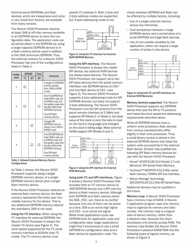
Using the I2C interface. When using the I2C interface for external EEPROM, the Neuron 5000 Processor is always the master I2C device (see Figure 2). The clock speed supported for the I2C serial memory interface is 400kHz (fast I2C mode). The I2C memory device must
specify I2C address 0. Both 1-byte and 2-byte address modes are supported, but 3-byte addressing mode is not.
SDA
3.3 V
_CS1~MISO
SCL
I 2 CSlave
(EEPROM)
Series5000 Chip
Figure 2: Using the I2C Interface for External NVM EEPROM Memory
Using the SPI interface. The Neuron 5000 Processor is always the master SPI device; any external NVM devices are always slave devices. The Neuron 5000 Processor can support up to two SPI slave devices from the serial memory interface: one EEPROM device at CS0~ and one flash device at CS1~ (see Figure 3). The Neuron 5000 Processor supports 2-byte addressing mode for SPI EEPROM devices, but does not support 3-byte addressing. The Neuron 5000 Processor runs the SPI protocol from the serial memory interface at 2.5MHz and supports SPI Mode 0. In Mode 0, the base value of the clock is zero; the data is read on the clock’s rising edge and changed on the clock’s falling edge. Most external NVMs support SPI Modes 0 and 3.
SPISlave
(EEPROM)
SCKMOSIMISO
SPISlave
(Flash)
CS0~SDA_CS1~
Series5000 Chip
Figure 3: Using the SPI Interface for External NVM Memories
Using both I2C and SPI interfaces. Figure 4 shows a Neuron 5000 Processor that includes both an I2C memory device (a 2KB EEPROM device) and a SPI memory device (a flash memory device). Although both EEPROM and flash memory share the SDA_CS1~ pin, there is no conflict because only one of them can be active at a time. SDA is an active high signal and CS1~ is an active low signal. While small applications could use EEPROM both for application code and configuration data, larger applications might find it economical to use a small EEPROM for configuration data and a flash device for application code. The
choice between EEPROM and flash can be affected by multiple factors, including:
• Use of a single external memory versus two memories.
• Cost comparison between a large EEPROM device and a combination of a small EEPROM and large flash devices.
• Use of non-volatile variables by the application, which can require a large number of writes to the device.
SCKMOSIMISO
CS0~SDA_CS1~SCL
I 2 CSlave
(EEPROM)
SPISlave(Flash)
Series5000 Chip
3.3 V
Figure 4: Using both I2C and SPI Interfaces for External NVM Memories
Memory devices supported. The Neuron 5000 Processor supports any EEPROM device that uses the SPI or I2C protocol, and meets the clock speed and addressing requirements described above.
While all EEPROM devices have a uniform write procedure, flash devices from various manufacturers differ slightly in their write procedure. Thus, a small library routine is stored in the external EEPROM device that helps the system write successfully to the external flash device. Echelon has qualified the following SPI flash memory devices for use with the Neuron 5000 Processor:
• Atmel® AT25F512B 512-Kilobit 2.7-volt Minimum SPI Serial Flash Memory.
• Numonyx™ M25P05-A 512-Kbit, serial flash memory, 50MHz SPI bus interface.
• Silicon Storage Technology SST25VF512A 512 Kbit SPI Serial Flash.
Additional devices may be qualified in the future.
Memory map. A Neuron 5000 Processor has a memory map of 64KB. A Neuron C application program uses this memory map to organize its memory and data access. The memory map is a logical view of device memory, rather than a physical view, because the chip’s processors only directly access RAM. The memory map divides the Neuron 5000 Processor’s physical 64KB RAM into the following types of logical memory, as shown in Figure 5:
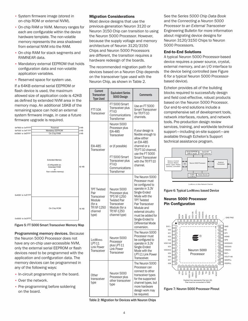
4
• System firmware image (stored in on-chip ROM or external NVM).
• On-chip RAM or NVM. Memory ranges for each are configurable within the device hardware template. The non-volatile memory represents the area shadowed from external NVM into the RAM.
• On-chip RAM for stack segments and RAMNEAR data.
• Mandatory external EEPROM that holds configuration data and non-volatile application variables.
• Reserved space for system use.If a 64KB external serial EEPROM or flash device is used, the maximum allowed size of application code is 42KB as defined by extended NVM area in the memory map. An additional 16KB of the remaining space can hold an external system firmware image, in case a future firmware upgrade is required.
ReservedMandatory EEPROM
On-Chip RAM
Extended Memory
(Configurable as:Extended RAM
or Non-volatile memory)
On-Chip ROM
0x0000 to 0x3FFF
0x4000 to 0xE7FF
0xE800 to 0xEFFF0xF000 to 0xF7FF0xF800 to 0xFFFF 2 KB
2 KB2 KB
42 KB
16 KB
Figure 5: FT 5000 Smart Transceiver Memory Map
Programming memory devices. Because the Neuron 5000 Processor does not have any on-chip user-accessible NVM, only the external serial EEPROM or flash devices need to be programmed with the application and configuration data. The memory devices can be programmed in any of the following ways:
• In-circuit programming on the board.• Over the network.• Pre-programming before soldering
on the board.
Migration ConsiderationsMost device designs that use the previous-generation Neuron 3120 or Neuron 3150 Chip can transition to using the Neuron 5000 Processor. However, because the supply voltage and memory architecture of Neuron 3120/3150 Chips and Neuron 5000 Processors are different, the transition requires a hardware redesign of the boards.
The recommended migration path for devices based on a Neuron Chip depends on the transceiver type used with the Neuron Chip, as shown in Table 2.
Current Transceiver Type Used
Equivalent Series 5000 Design Comments
FTT-10A Transceiver
FT 5000 Smart Transceiver plus FT-X3 Communications Transformer
Use an FT 5000 Smart Transceiver for TP/FT-10 channels.
EIA-485 Transceiver
Neuron 5000 Processor plus EIA-485 Transceiver
or (if possible)
FT 5000 Smart Transceiver plus FT-X3 Communications Transformer
If your design is flexible enough to allow either an EIA-485 channel or a TP/FT-10 channel, use the FT 5000 Smart Transceiver with the TP/FT-10 channel.
TPT Twisted Pair Transceiver Module (for a TP/XF-1250 channel type)
Neuron 5000 Processor plus TPT/XF-1250 Twisted Pair Transceiver Module (for a TP/XF-1250 channel type)
The Neuron 5000 Processor must be configured to operate in 3.3V Single-Ended Mode with the TPT Twisted Pair Transceiver Module and external circuitry must be added for Single-Ended to Differential Mode conversion.
LonWorks LPT-11 Link Power Transceiver
Neuron 5000 Processor plus LPT-11 Link Power Transceiver
The Neuron 5000 Processor must be configured to operate in 3.3V Single-Ended Mode with the LPT-11 Link Power Transceiver.
Other transceiver type
Neuron 5000 Processor plus other transceiver type
The Neuron 5000 Processor can connect to other transceiver types for the supported channel types, but more hardware design work may be required.
Table 2: Migration for Devices with Neuron Chips
See the Series 5000 Chip Data Book and the Connecting a Neuron 5000 Processor to an External Transceiver Engineering Bulletin for more information about migrating device designs for Neuron 3120/3150 Chips to Neuron 5000 Processors.
End-to-End SolutionsA typical Neuron 5000 Processor-based device requires a power source, crystal, external memory, and an I/O interface to the device being controlled (see Figure 6 for a typical Neuron 5000 Processor-based device).
Echelon provides all of the building blocks required to successfully design and field cost-effective, robust products based on the Neuron 5000 Processor. Our end-to-end solutions include a comprehensive set of development tools, network interfaces, routers, and network tools. Pre-production design review services, training, and worldwide technical support—including on-site support—are available through Echelon’s Support technical assistance program.
Crystal (10 MHz)
Power Source
Serial EEPROM (2KB or larger)
I/O
LONWORKS or other Network Channel
Neuron 5000 Processor ExternalTransceiver
Sense or ControlDevices: Motors,
Valves, Lights, Relays,Switches, Controllers
Serial SPIFlash (optional)
Figure 6: Typical LonWorks based Device
Neuron 5000 Processor Pin Configuration
Neuron 5000Processor
1
2
3
4
5
6
7
8
9
10
11
12
36
35
34
33
32
31
30
29
28
27
26
25
GND
NC
CP1
AGND
GP0
AVDD3V3
VDD3V3
VIN3V3
RST~
VOUT1V8
GNDPLL
VDDPLL
GND PAD
Dashed line represents Pad (pin 49)Pad must be connected to GND
SVC~
IO0
IO1
IO2
IO3
VDD1V8
IO4
VDD3V3
IO5
IO6
IO7
IO8
13 14 15 16 17 18 19 20 21 22 23 24
IO9
IO10
IO11
VDD
1V8
TRST
~
VDD
3V3
TCK
TMS
TDI
TDO
XIN
XOU
T
48 47 46 45 44 43 42 41 40 39 38 37
MO
SI
SCK
MIS
O
SCL
VDD
1V8
SDA_
CS1
~
VDD
3V3
VDD
3V3
CS0
~
CP4
CP3
CP2
Figure 7: Neuron 5000 Processor Pinout

5
Neuron 5000 Processor Pin DescriptionsAll digital inputs are low-voltage transistor-transistor logic (LVTTL) compatible, low leakage, 5V-tolerant. All digital outputs are slew-rate limited to reduce Electromagnetic Interference (EMI) concerns.
Pin Name
Pin Number Type Description
SVC~ 1 Digital I/O Service (active low)
IO0 2 Digital I/O IO0 for I/O Objects
IO1 3 Digital I/O IO1 for I/O Objects
IO2 4 Digital I/O IO2 for I/O Objects
IO3 5 Digital I/O IO3 for I/O Objects
VDD1V8 6 Power1.8 V Power Input (from internal voltage regulator)
IO4 7 Digital I/O IO4 for I/O Objects
VDD3V3 8 Power 3.3 V Power
IO5 9 Digital I/O IO5 for I/O Objects
IO6 10 Digital I/O IO6 for I/O Objects
IO7 11 Digital I/O IO7 for I/O Objects
IO8 12 Digital I/O IO8 for I/O Objects
IO9 13 Digital I/O IO9 for I/O Objects
IO10 14 Digital I/O IO10 for I/O Objects
IO11 15 Digital I/O IO11 for I/O Objects
VDD1V8 16 Power1.8 V Power Input (from internal voltage regulator)
TRST~ 17 Digital Input
JTAG Test Reset (active low)
VDD3V3 18 Power 3.3 V Power
TCK 19 Digital Input JTAG Test Clock
TMS 20 Digital Input
JTAG Test Mode Select
TDI 21 Digital Input
JTAG Test Data In
TDO 22 Digital Output
JTAG Test Data Out
XIN 23 Oscillator In
Crystal oscillator Input
XOUT 24 Oscillator Out
Crystal oscillator Output
VDDPLL 25 Power1.8 V Power Input (from internal voltage regulator)
GNDPLL 26 Power Ground
VOUT1V8 27 Power1.8 V Power Output (of internal voltage regulator)
RST~ 28 Digital I/O Reset (active low)
VIN3V3 29 Power3.3 V input to internal voltage regulator
VDD3V3 30 Power 3.3 V Power
AVDD3V3 31 Power 3.3 V Power
Pin Name
Pin Number Type Description
CP0 32 Communi-cations
Single-Ended Mode: Receive serial dataSpecial Purpose Mode: Receive serial data
AGND 33 Ground Ground
CP1 34 Communi-cations
Single-Ended Mode: Transmit serial dataSpecial Purpose Mode: Transmit serial data
NC 35 N/A Do Not Connect
GND 36 Ground Ground
CP2 37 Communi-cations
Single-Ended Mode: External transceiver enableSpecial Purpose Mode: Bit clock
CP3 38 Communi-cations Do Not Connect
CP4 39 Communi-cations
Single-Ended Mode: Collision detectSpecial Purpose Mode: Frame clock
CS0~ 40 Digital I/O
SPI slave select 0 (CS0~, active low) (for external memory connection only)
VDD3V3 41 Power 3.3 V Power
VDD3V3 42 Power 3.3 V Power
SDA_CS1~ 43 Digital I/O
I2C: serial data (SDA)SPI: slave select 1 (CS1~, active low) (for external memory connection only)
VDD1V8 44 Power1.8 V Power Input (from internal voltage regulator)
SCL 45 Digital I/OI2C: serial clock (SCL) (for external memory connection only)
MISO 46 Digital I/O
SPI master input, slave output (MISO) (for external memory connection only)
SCK 47 Digital I/OSPI serial clock (SCK) (for external memory connection only)
MOSI 48 Digital I/O
SPI master output, slave input (MOSI) (for external memory connection only)
PAD 49 Ground Pad Ground
Table 3: Neuron 5000 Processor Pin Description
Electrical CharacteristicsNeuron 5000 Processor Operating Conditions
Param-eter1 Description Minimum Typical Maximum
VDD3 Supply voltage 3.00 V 3.3 V 3.60 V
VLVI
Low-voltage indicator trip
point2.70 V 2.96 V
TAAmbient
temperature -40° C +85° C
fXINXIN clock
frequency2 - 10,0000 MHz -
IDD3
Current consumption3
5MHz10MHz20MHz40MHz80MHz
9 mA9 mA
15 mA23 mA38 mA
15 mA15 mA23 mA33 mA52 mA
Table 4: Neuron 5000 Processor Operating Conditions
Notes1. All parameters assume nominal supply
voltage (VDD3 = 3.3 V ± 0.3 V) and operating temperature (TA between -40ºC and +85ºC), unless otherwise noted.
2. See Clock Requirements in the Series 5000 Chip Data Book for more detailed information about the XIN clock frequency.
3. Assumes no load on digital I/O pins, and that the I/O lines are not switching.
Digital Pin CharacteristicsThe digital I/O pins (IO0–IO11) have LVTTL-level inputs. Pins IO0–IO7 also have low-level-detect latches. The RST~ and SVC~ pins have internal pull-ups, and the RST~ pin has hysteresis.
Table 5 below lists the characteristics of the digital I/O pins, which include IO0–IO11, CP0- CP4 and the other digital pins listed in Table 3.
Param-eter1 Description Mini-
mum Typical Maxi-mum
VOHOutput drive high
at IOH = 8 mA 2.4 V VDD3
VOLOutput drive low
at IOL = 8 mA GND 0.4 V
VIH Input high level 2.0 V 5.5 VVIL Input low level GND 0.8 V
VHYSInput hysteresis
for RST~ pin300 mV
IINInput leakage
current - 10 µA
RPUPullup
resistance213 kΩ
23 kΩ
IPUPullup current
when pin at 0 V2130 µA
275 µA
Table 5: Neuron 5000 Processor Digital Pin Characteristics
6
Notes1. All parameters assume nominal supply
voltage (VDD3 = 3.3 V ± 0.3 V) and operating temperature (TA between -40ºC and +85ºC), unless otherwise noted.
2. Applies to RST~ and SVC~ pins only.
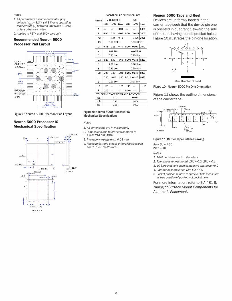
Recommended Neuron 5000 Processor Pad Layout
Figure 8: Neuron 5000 Processor Pad Layout
Neuron 5000 Processor IC Mechanical Specification
Figure 9: Neuron 5000 Processor IC Mechanical Specifications
Notes
1. All dimensions are in millimeters.2. Dimensions and tolerances conform to
ASME Y14.5M.-1994.3. Package warpage max. 0.08 mm.4. Package corners unless otherwise specified
are R0.175±0.025 mm.
Neuron 5000 Tape and Reel Devices are uniformly loaded in the carrier tape such that the device pin one is oriented in quadrant 1 toward the side of the tape having round sprocket holes. Figure 10 illustrates the pin-one location.
User Direction of Feed
Figure 10: Neuron 5000 Pin One Orientation
Figure 11 shows the outline dimensions of the carrier tape.
Figure 11: Carrier Tape Outline DrawingAo = Bo = 7.25 Ko = 1.10
Notes1. All dimensions are in millimeters.2. Tolerances unless noted: 1PL + 0.2. 2PL + 0.13. 10 Sprocket hole pitch cumulative tolerance +0.24. Camber in compliance with EIA 481.5. Pocket position relative to sprocket hole measured
as true position of pocket, not pocket hole.
For more information, refer to EIA-481-B, Taping of Surface Mount Components for Automatic Placement.
7
Copyright © 2007-2011, Echelon Corporation. Echelon, LonWorks, Neuron, 3120, 3150, and NodeBuilder are trademarks of Echelon Corporation registered in the United States and/or other countries. LonSupport is a trademark of Echelon Corporation. Other trademarks belong to their respective holders. Content subject to change without notice. P/N 003-0458-1B
Figure 12 shows the Neuron 5000 Series 13” Reel Drawing and Specification.
Figure 12: Neuron 5000 10” Reel and Hub Drawing
Figure 13 shows the 5000 Series 7” Reel Drawing and Specification.
Figure 13: Neuron 5000 7” Reel and Hub Drawing
SPECIFICATIONS
RoHS-Compliant The Neuron 5000 Processor is compliant with the European Directive 2002/95/EC on the restriction of the use of certain hazardous substances (RoHS) in electrical and electronic equipment.
EMC Specifications depend on the network transceiver used with the Neuron 5000 Processor.
Transmission Speed Depends on network transceiver: 78 kbit/s for TP/FT-10 channel; 1250 kbit/s for TP/XF-1250 channel. (See EIA-485 channel specification for transmission speed characteristics.)
Operating Temperature -40 to 85°C
Reflow Soldering Temperature Profile Refer to Joint Industry Standard document IPC/JEDEC J-STD-020D.1 (March 2008).
Peak Reflow Soldering Temperature 260°C
ORDERING INFORMATION
Neuron 5000 Processor 14305R-2000 14305R-500