Neuro-transmitter (EEG) Interface System
50
Neuro-transmitter (EEG) Interface System Design Review ECE 445: Senior Design Group #29 Kevin Armstrong-John Burton-Alex Lostumbo TA: Ryan May October 4, 2012
Transcript of Neuro-transmitter (EEG) Interface System
Neuro-transmitter (EEG) Interface System Design Review
ECE 445: Senior Design
Group #29
Kevin Armstrong-John Burton-Alex Lostumbo
TA: Ryan May
October 4, 2012

Neuro-transmitter 2 Fall 2012 (EEG) Interface System
Table of Contents
Neuro-transmitter (EEG) Interface System.................................................................................... 1
ECE445: Senior Design ..............................................................................……........................... 1
Table of Contents ....................................................................................…................................... 2
1 Introduction .....................................................................................…….................................... 3
1.1 Statement of Purpose..................................................................………….............................. 3
1.2 Objectives ..................................................................................……...................................... 3
1.2.1 Goals ..............................................................................……………................................... 3
1.2.2 Functions………………………………………………………………………...…………. 3
1.2.3 Benefits ..................................................................………................................................... 3
1.2.4 Features……………………………………………………………………………...………3
2 Design.......................................................................................................................................... 4
2.1 Block Diagrams ...............……………………………………................................................ 4
2.1.1 Power Supply ……………………………………………………………………….………8
2.1.2 Sensor Impedance Verification System……………………………………………………10
2.1.3 The Arduino System……………………………………………………….………………15
2.1.3.1 SD Card Memory Feedback Diagram……………………………………..……………..15
2.1.3.2 Clock Management and Selection System…………………………………...…………..18
2.1.4 Amplifier………………………………………………………………………..………….22
2.1.5 Filter……………………………………………………………………………..…………24
2.2 Performance Requirements..................................................................................................... 26
2.3 Simulations.........................................................................................………………….........30
2.3.1 Power Supply Systems………………………………………………………………..……30
2.3.2 Sensor Impedance Verification System……………………………………………..……..31
2.3.3 Amplification Simulations…………………………………………………………………36
2.3.4 Filter Simulations and Bode Plot……………………………………………..……………40
3 Verifications..................................................................................………………..................... 45
4. Cost Analysis….............................................………………………………………..…..........45
4.1 Labor....................................……………………………………………………....................45
4.2 Cost.................................................……………………………............................................ 45
4.3 Grand Total.......................................……………………………….......................................47
4.4 Schedule ...........................................………………………………...................................... 47
5 Engineering Ethics ...................................…………………………......................................... 49
6 Resources.....................................................………….............................................................. 50

Neuro-transmitter 3 Fall 2012 (EEG) Interface System
I. Introduction
1.1 Statement of Purpose
The purpose of this project is to reduce the cost of and improve the efficiency of current
Electroencephalography(EEG) systems. At the moment, low-cost EEG systems can run over
$800. Our system will cost under $500, and allow the end user to record brain activity without
the presence of a laptop. The current market for EEG systems is in high demand both in
neurological research and the medical industry. The devices on the market today require that one
carries around a laptop in order to record data. We will rid the necessity to carry a laptop. Along
with using a cheaper device design, we will make our device more mobile and more cost-
efficient thus creating a very viable product in the EEG market. Our device will not just replicate
other similar devices on the market. Our device is a data logging system that will serve as a more
economical alternative that adds convenience to traditional EEG systems.
1.2 Objectives
1.2.1 Goals
· Create a fully functional EEG that logs time-stamped data on an SD card
· Keep within a budget of $500
· Meet the ethical and safety requirements and quality of data for research
· SD card should hold at least 2 hours of data logging information
1.2.2 Functions
· 10,000 gain Op-amps to detect and differentiate between voltages produced by brain
waves
· Bandpass filtering to remove frequency noise from environment and subconscious
controls
· Analog to digital converter that also timestamps and stores the digitized information
· LED display to verify sensors are making the correct contact by measuring their
impedances
1.2.3 Benefits
· Making EEG mobile for novel neuroscience research
· Lowering barrier of entry for smaller neuroscience budgets to conduct field research
· Indication in the field of good sensor contact with the research participant's head
· Circuitry involved will be light and packaged for portable usage
1.2.4 Features
· SD card storing at least 2GB of memory equating to at least an hour’s worth of research
· Power supply that lasts at least 5 hours
· We have dual color LEDs that tell us if the sensors are applied properly (impedances are
less that 20 kΩ
· All sensors will pass through a common amplification and filtering component,
reducing irregularities

Neuro-transmitter 4 Fall 2012 (EEG) Interface System
II. Design
2.1 Block Diagrams
Overall EEG Functional Block Diagram:
*Figure Note: The MUX Regulator Module and Digital/Save module are contained in one Arduino device, but
are written in two separate blocks for the reader’s clarity
Figure 1a. Overall functional summary layout. Overall Functional Summary:
The large-scale block diagram describes the connection between the sensors in the EEG
cap (listed here as “sensor bay”) and our physical device encased in an acrylic box that will be
provided by the Electronics shop and be strapped to the back of the EEG cap user. To ensure that
the sensors are properly applied to the user, we plan to implement an Impedance Verification
System in order to assure both the user and the researcher that the quality of the data being
collected is accurate for the experimentation. The amplifier module will take in the signals from
the sensors and amplify them in order to bring the voltages into normal detectable levels for the
ADC to differentiate between the signals voltages. From the amplifier module, a filter module
will remove the noise from each signal and leave the resulting data signal information that we
need to store in the SD card. Both the amplifier and filter modules will take place on a PCB
board. After filtering out the noise from each sensor, the individual sensor signals will be fed into
the Digital/Save Module to store the data by signal. The ADC will convert the data with a
resolution quality great enough to accurately differentiate between the different voltages that
occur. The SD card and Arduino memory module will organize the signal information by sensor
channel.
Neuro-transmitter 5 Fall 2012 (EEG) Interface System
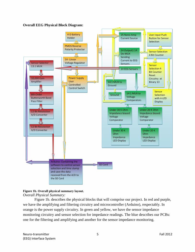
Overall EEG Physical Block Diagram:
Figure 1b. Overall physical summary layout.
Overall Physical Summary: Figure 1b. describes the physical blocks that will comprise our project. In red and purple,
we have the amplifying and filtering circuitry and microcontroller (Arduino), respectably. In
orange is the power supply circuitry. In green and yellow, we have the sensor impedance
monitoring circuitry and sensor selection for impedance readings. The blue describes our PCBs:
one for the filtering and amplifying and another for the sensor impedance monitoring.

Neuro-transmitter 6 Fall 2012 (EEG) Interface System
Power Supply:
In our power supply block, we plan to start with a high voltage and step down by means
of resistive elements between the blocks if needed. The overall power supply will consist of four
D batteries that at initial use will have 6 volts of power. This voltage will then be wired to a
PMOSFET in such a way that the PMOSFET will be connected with the batteries going to the
drain, the source going to the rest of the circuit, and the gate connected to ground. This setup will
ensure the transistor will only be on when the voltage is attached the right way, and will be off
otherwise. The reason for this and not a diode is a matter of safety to the research participant that
will be wearing this. Diodes lose more power and thus generate more heat that could be
hazardous. The PMOS on the other hand will generate far less heat and power loss and thus be
safer and more efficient. From the PMOS, the power will go through a linear voltage regulator.
The purpose for the linear voltage regulator is to ensure that even as the batteries lose volts
before they no longer function, the voltage regulator will keep outputting a constant voltage of 5
volts. Thus the power supply to the rest of the system will not vary randomly and cause distortive
effects. From the linear voltage regulator, the power will go to a switch that will be manually set
to feed the power into either the data processing and logging circuitry, or feeding the power into
the Sensor impedance verification circuitry.
MUX Module:
The MUX module will take input from the sensor bay and one output to the amplification
component. For choosing which signal will pass through the MUX, the Arduino will send a
signal command in the MUX’s SELECT bits. On a macro level, there will be a 16-to-1 MUX
provided by analog systems (described in greater detail later in report) that will choose which of
the 16 inputs should be outputted to the Arduino. Since we only use thirteen of the sixteen inputs,
we will set three of the sixteen to ground, and alternate selection between the signals being sent
to the Arduino. The block will go through the sensor inputs one at a time and connect the output
to the amplification component. The purpose of this block is to reduce the amount of circuitry
involved to amplify and filter all 13 sensor's signals.
Amplifier Module:
The amplifier module will take its inputs from the 13 sensors in the head cap, and will
send its outputs to the Filter module. It will consist of an operational amplifier that will take in
voltages between 20-200 micro-volts and output voltages from 0.2-2.00 voltages. It will
primarily be composed of resistors and two cascaded operational amplifiers designed to give
10,000 gain for the range of input voltages. The reason for cascading them is to ensure the slew
rate is never exceeded in how fast the output voltages need to change relative to the input
voltages. This amplification will be done to ensure the ADC can properly differentiate between
the types of voltage values to convert. This will specifically be a non-inverting output.
Filter Module:
The filter model will consist of an 8th order Butterworth band pass filter circuit that will
remove signals with frequencies above 50 Hz and below 0.16 Hz, while minimizing any
reduction in the signal amplitude of those frequencies that are between the two. It will take
inputs from the amplifier module and send its outputs to the MUX module. It will primarily be
composed of a high pass filter in series with a low pass filter that will be composed of resistors,
capacitors, and operational amplifiers. The exact values of the resistors and capacitors will be

Neuro-transmitter 7 Fall 2012 (EEG) Interface System
determined by the Butterworth equation.
Digital/Save Module (Memory module):
The memory module will consist of three devices, an A/D converter, the Arduino board,
and a 2GB SD card. It will also consist of a DeMUX that will take its inputs from the output of
the A/D converter and send the output to the Arduino board to one of the 13 different output
lines that correspond to the 13 sensors used. The DeMUX will be synchronized with the MUX so
the sensor currently selected will be passed through amplification, filtering, A/D conversion, and
then get put on the specific sensor signal channel on the Arduino to get stored on the SD card.
The Arduino attaches a timestamp to each signal and stores the signal in the memory card. This
data would be accessible from the memory card by means of a USB cable connection from a
computer to the Arduino board.
Sensor Impedance Verification System:
The Sensor Impedance Verification System will monitor the impedance on each of the
sensors one at a time before the user begins data logging. The user will put on the sensor cap and
apply all of the sensors to the best of their knowledge then user the impedance verification to
make sure he or she applied the sensors correctly. The system will need to be switched on before
using and switched off afterwards to not interfere with data collection. The system will have 4
parts: a current source, a selection circuit, a comparator circuit, and the Counter and LED display
unit. The current source will supply a small current (in the order of nA) that will be sent to the
skin. We will read the voltage over the sensor-skin contact of each sensor (chosen by the
selection circuit), and compare those to known voltages that correspond to known impedances
(20k and 30k). We will display two LEDs to show the relative impedance. The chosen sensor
will also be shown in binary using 4 LEDs. The user has control of the changing rate of sensors
and can change them using the button provided that will up-count the sensor number. The system
in itself will provide a visual to tell the user if each sensor is correctly applied.
Neuro-transmitter 8 Fall 2012 (EEG) Interface System
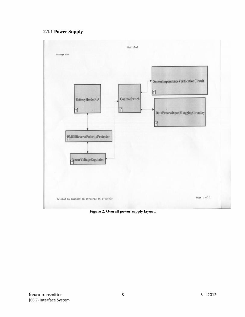
2.1.1 Power Supply
Figure 2. Overall power supply layout.

Neuro-transmitter 9 Fall 2012 (EEG) Interface System
Figure 3. Reverse polarity protection circuit.
Overall Summary:
The power supply for our system takes a voltage input of 5.4 - 6.6 Vdc supplied by 4 D
batteries. The power supply utilizes a PMOS transistor with the drain connected to Vin+, the gate
connected to ground and the source connected to our load. The purpose of this PMOS transistor
is to protect our circuit from a human failure or inserting the voltage source in backwards. When
the voltage is correctly attached (correct polarity), the PMOS turns on and lets current flow
through the circuit. When the voltage source is in reverse polarity, the PMOS turns off and the
circuit in fact doesn’t blow up like it would without the PMOS for protection. The novelty
behind this is it protects the circuit from a possible human error in inserting the voltage source in
reverse polarity because the PMOS will not conduct.
Further analysis...
With a forward biased voltage source:
Vgs = (Vg-Vs) = 0 - 6 = -6V
-If Vgs is -4V or less the PMOS transistor will turn on thus conducting current.
With the reverse polarity voltage source:
(First assume MOSFET is turned on.)
Vgs = (Vg-Vs) = 0 - (-12) = +12V
Vgs must be -4V or less in order for the PMOS transistor to turn on which is not true here. The
transistor must be off and therefore not conducting current. The circuit is safe.
Another important addition to our circuit is the inclusion of a low-dropout regulator. This
component will take an input voltage from a source that can be characterized as unstable and
make it stable. To be more precise, in our circuit our Vin from the 4 D batteries will be around 6
V. The low-dropout regulator will take this value and stabilize it at a level it can hold for longer.
Neuro-transmitter 10 Fall 2012 (EEG) Interface System
The low-dropout regulator will keep our input voltage at a stable level of 5V +-10% = 4.5-5.5V.
By doing this we will be dissipating less power in the regulator than you would if you used
another type of regulator.
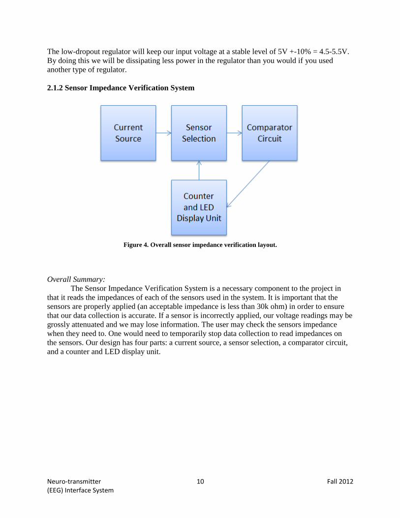
2.1.2 Sensor Impedance Verification System
Figure 4. Overall sensor impedance verification layout.
Overall Summary:
The Sensor Impedance Verification System is a necessary component to the project in
that it reads the impedances of each of the sensors used in the system. It is important that the
sensors are properly applied (an acceptable impedance is less than 30k ohm) in order to ensure
that our data collection is accurate. If a sensor is incorrectly applied, our voltage readings may be
grossly attenuated and we may lose information. The user may check the sensors impedance
when they need to. One would need to temporarily stop data collection to read impedances on
the sensors. Our design has four parts: a current source, a sensor selection, a comparator circuit,
and a counter and LED display unit.

Neuro-transmitter 11 Fall 2012 (EEG) Interface System
Figure 5. Overall current source layout.
Current Source:
The first block within the sensor impedance verification system is the current source. The
safety of our users and the security of the sensors are the two most important design criteria for
this block. We must ensure that we do not send too much current through the sensors (the Grass
Electrode Sensors can only tolerate less than 1 microamp of current). Current through the skin is
also a concern in that too large of a current can severely harm a person. Greater than 1 mA can
lead to severe burns, paralysis, or even death. Because we know that the impedance of the skin is
somewhere between 5k ohms and 50k ohms, we put a much larger impedance in series with the
impedance of the skin to make sure that the current would be constant and small coming off the
battery and that there was no way the skin and sensors would be subjected to a large voltage drop.
Note: The current sensor is selected in the Sensor Selection block
Vin / (R+Zskin) = i
5V / (200M ohm + 5k ohm) = i = 2.499E-8 A---->max current expected
5V / (200M ohm + 50k ohm) = i = 2.499E-8 A ---->min current expected
*Note: the current is constant.
The current source must be constant because in the comparator circuit, we compare the voltage
over the skin-sensor contact to voltages calculated that assume a constant current of 25 nA. We
are comparing the voltages, not direct impedances. To do this we must have a known current and

Neuro-transmitter 12 Fall 2012 (EEG) Interface System
using ohms law we can determine which voltages would correspond to which impedances.
Figure 6. Overall sensor selection layout.
Sensor Selection:
The sensor selection circuit lets the user control which sensor the sensor impedance
verification system is reading. The block consists of a push button to control a clock of a counter
that up counts current sensor on the push. The counter will count from 0 up to 13 and reset to 0.
The circuit will then display which sensor is current by lighting up LEDs that display a number
in binary. We would like to read the voltages off of the current sensor and in order to do that we
need a circuit that requires two MUXs and a DeMUX. The switches on each of the MUXs and
the DeMUX will be controlled by the counter. The first MUX takes in the current driven by the
5Vdc battery and the 200M ohm resistor. The current is then driven to the current sensor chosen
by the counter. The sensor must then go to ground. Our sensors only need to be grounded when
checking impedance. In fact we do not want our sensors to be grounded during data collection. In
order to accomplish this, the other node of each of the sensors then goes into the inputs of a
MUX. The current sensor is chosen by the counter and the output of that MUX goes to ground.
Because we want to read the voltages across each of the sensors, another MUX reads the
voltages of the sensors. The MUX chooses the current sensor and its voltage is sent to the
comparator circuit.
Neuro-transmitter 13 Fall 2012 (EEG) Interface System
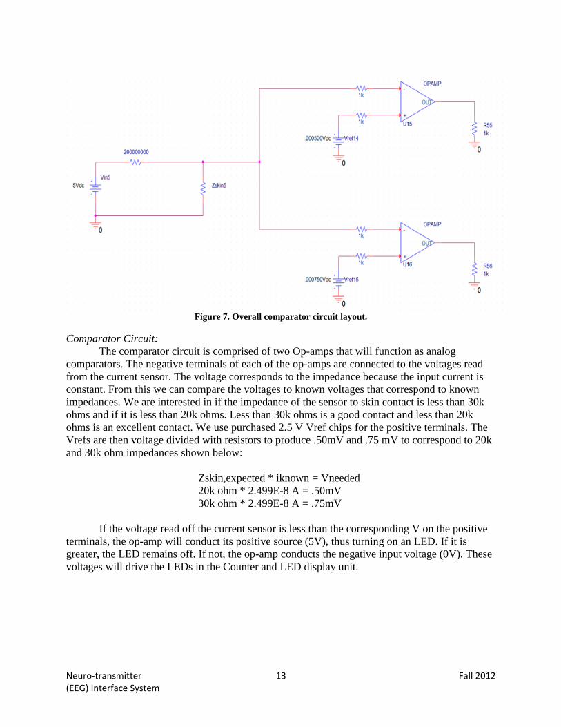
Figure 7. Overall comparator circuit layout.
Comparator Circuit:
The comparator circuit is comprised of two Op-amps that will function as analog
comparators. The negative terminals of each of the op-amps are connected to the voltages read
from the current sensor. The voltage corresponds to the impedance because the input current is
constant. From this we can compare the voltages to known voltages that correspond to known
impedances. We are interested in if the impedance of the sensor to skin contact is less than 30k
ohms and if it is less than 20k ohms. Less than 30k ohms is a good contact and less than 20k
ohms is an excellent contact. We use purchased 2.5 V Vref chips for the positive terminals. The
Vrefs are then voltage divided with resistors to produce .50mV and .75 mV to correspond to 20k
and 30k ohm impedances shown below:
Zskin,expected * iknown = Vneeded
20k ohm * 2.499E-8 A = .50mV
30k ohm * 2.499E-8 A = .75mV
If the voltage read off the current sensor is less than the corresponding V on the positive
terminals, the op-amp will conduct its positive source (5V), thus turning on an LED. If it is
greater, the LED remains off. If not, the op-amp conducts the negative input voltage (0V). These
voltages will drive the LEDs in the Counter and LED display unit.

Neuro-transmitter 14 Fall 2012 (EEG) Interface System
Figure 8. Overall Counter and LED display unit layout.
Counter and LED Display Unit:
The Counter and LED display unit will contain six LEDs. Two green LEDs will
correspond to <20k ohms and <30k ohms. If two green LEDs appear, you have excellent contact.
If only one appears, you have sufficient contact. If neither LED appears, the impedance is above
the accepted value, 30k ohms. The remaining 4 LEDs will display the current sensor number in
binary (0-13). The display will show the current sensor number given by the outputs of the
counter. The counter is also grouped within this block. The counter contains the number of the
current sensor being monitored and is controlled by the user via a push button. This allows the
user to scroll through the sensors at the user’s own pace in order to check each sensor’s contact
impedance. The counter will count from 0 up to 13 and then reset back to 0. The counter’s
outputs will be sent to the LEDs for binary display as well as to the Sensor Selection circuit.

Neuro-transmitter 15 Fall 2012 (EEG) Interface System
2.1.3 The Arduino System 2.1.3.1 SD Card Memory Feedback Diagram:
Figure 9. The Arduino microcontroller.

Neuro-transmitter 16 Fall 2012 (EEG) Interface System
*Reproduced from the Arduino Ethernet Shield page
Figure 10. The SD library included with the Arduino.

Neuro-transmitter 17 Fall 2012 (EEG) Interface System
Figure 11. Overall SD Memory Feedback layout.
Overall Summary:
In the 6”x6”x6” enclosure provided by the Electronics Shop, there will be an opening for the
user to insert and remove the 2GB SD card. Within the enclosure, there is a separate
compartment slot for the SD card reader, allowing the users access to insert and remove the SD
card. The single signal output from the MUX will be fed into the Arduino board(represented here
as SD Card I/O Module) that will timestamp each signal as it is selected one-by-one and store the
signals onto a 2GB SD card. The specifics regarding MUX signal selection will be explained in
greater detail later in this report.
SD Card I/O:
Our I/O device for the sensor signals will be amplified and filtered, and then each of the
signals will go into the Arduino board, where each signal is time stamped and stored on to the
2GB SD card.
SD Card:
This is a standard 2GB SD card that will hold at least 1.5 hours’ worth of sensor data. The
user would be able to unlock this data by means of the Arduino SDLibrary (described above),
and a USB-to-Ethernet adapter connection that links the Arduino board to the computer.
Neuro-transmitter 18 Fall 2012 (EEG) Interface System
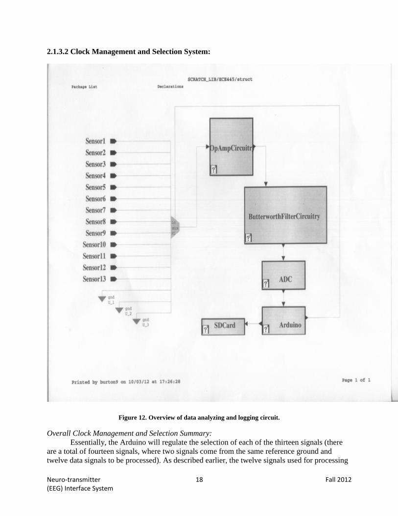
2.1.3.2 Clock Management and Selection System:
Figure 12. Overview of data analyzing and logging circuit.
Overall Clock Management and Selection Summary:
Essentially, the Arduino will regulate the selection of each of the thirteen signals (there
are a total of fourteen signals, where two signals come from the same reference ground and
twelve data signals to be processed). As described earlier, the twelve signals used for processing
Neuro-transmitter 19 Fall 2012 (EEG) Interface System
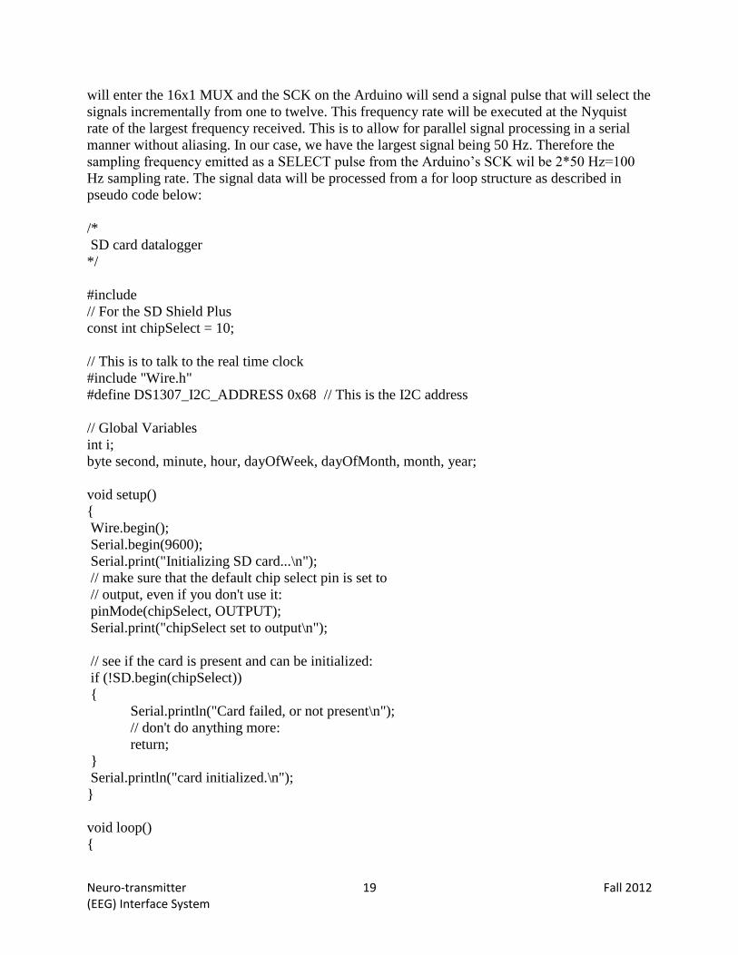
will enter the 16x1 MUX and the SCK on the Arduino will send a signal pulse that will select the
signals incrementally from one to twelve. This frequency rate will be executed at the Nyquist
rate of the largest frequency received. This is to allow for parallel signal processing in a serial
manner without aliasing. In our case, we have the largest signal being 50 Hz. Therefore the
sampling frequency emitted as a SELECT pulse from the Arduino’s SCK wil be 2*50 Hz=100
Hz sampling rate. The signal data will be processed from a for loop structure as described in
pseudo code below:
/*
SD card datalogger
*/
#include
// For the SD Shield Plus
const int chipSelect = 10;
// This is to talk to the real time clock
#include "Wire.h"
#define DS1307_I2C_ADDRESS 0x68 // This is the I2C address
// Global Variables
int i;
byte second, minute, hour, dayOfWeek, dayOfMonth, month, year;
void setup()
{
Wire.begin();
Serial.begin(9600);
Serial.print("Initializing SD card...\n");
// make sure that the default chip select pin is set to
// output, even if you don't use it:
pinMode(chipSelect, OUTPUT);
Serial.print("chipSelect set to output\n");
// see if the card is present and can be initialized:
if (!SD.begin(chipSelect))
{
Serial.println("Card failed, or not present\n");
// don't do anything more:
return;
}
Serial.println("card initialized.\n");
}
void loop()
{

Neuro-transmitter 20 Fall 2012 (EEG) Interface System
// make a string for assembling the data to log:
String dataString = getDateDs1307();
dataString += String(",");
// read three sensors and append to the string:
for (int analogPin = 0; analogPin < 3; analogPin++)
{
int sensor = analogRead(analogPin);
dataString += String(sensor);
if (analogPin < 2)
{
dataString += ",";
}
}
// open the file. note that only one file can be open at a time,
// so you have to close this one before opening another.
File dataFile = SD.open("datalog.csv", FILE_WRITE);
// if the file is available, write to it:
if (dataFile)
{
dataFile.println(dataString);
dataFile.close();
// print to the serial port too:
Serial.println(dataString);
}
// if the file isn't open, pop up an error:
else
{
Serial.println("error opening datalog.csv");
}
delay(100);
SCK=100;
Neuro-transmitter 21 Fall 2012 (EEG) Interface System
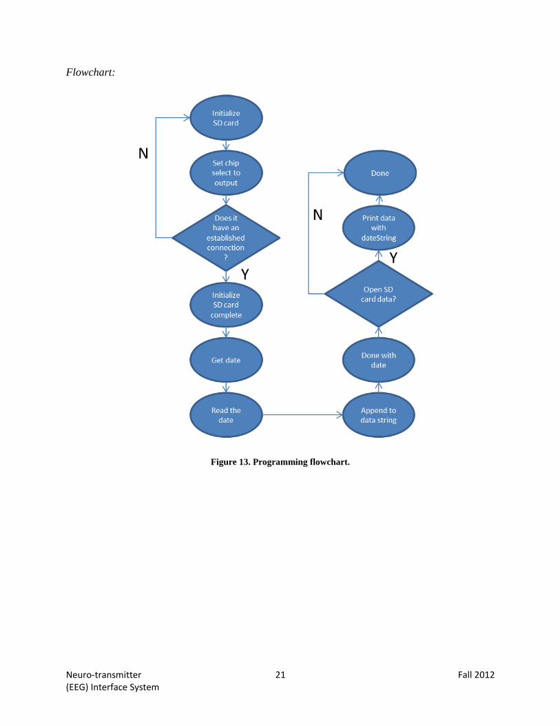
Flowchart:
Figure 13. Programming flowchart.
Neuro-transmitter 22 Fall 2012 (EEG) Interface System
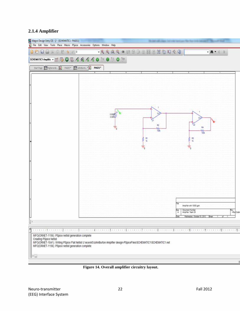
2.1.4 Amplifier
Figure 14. Overall amplifier circuitry layout.

Neuro-transmitter 23 Fall 2012 (EEG) Interface System
Overall Amplifier Summary:
The amplifier takes in voltage signals of about 20 to 200 microvolts and output voltages
with between 0.2to 2 volts. This is done so that the A/D can easily differentiate between the
different voltage levels with a certain amount of resolution. In order to make this happen, there
needs to be a 10,000 gain from the input voltage to the output voltage. Theoretically this could
have been done in one stage, however most amplifiers operate with gains around 100 and as such
it makes more sense to cascade the two stages. To calculate the gain we do the following:
The calculation centers on the fact that the voltage at both the positive and negative
inputs is the same. This arises from the fact that the gain of the amplifier is exceedingly high. If
the output of the circuit remains within rails of the supply voltage of the amplifier, then the
output voltage divided by the gain means that there is virtually no difference between the two
inputs.
As the input to the op-amp draws virtually no current, the current flowing in the resistors
R1 and R2 is the same. The voltage at the inverting input is formed from a potential divider
consisting of R1 and R2, and as the voltage at both inputs is the same, the voltage at the inverting
input must be the same as that at the noninverting input. This means that Vin = Vout x R1 / (R1
+ R2). Hence the voltage gain of the circuit A can be taken as: A = Vout/Vin = (R1+R2)/R1= (R1)/(R1) + (R2)/(R1) = 1 + R2 / R1
And if R2/R1 is much greater than 1 then A approximatly equals R2/R1. Now we can see how cascading works. This Vout will become the Vin2 for the next stage of the
circuit. Thus:
Vin2 = Vout2 x R3/(R3+R4) A2 = Vout2/Vin2 = 1 + R4/R3
But we want Vout2/Vin to get Atotal. Thus:
Vin2 = Vout = Vout2 x R3/(R3+R4) = Vin x (1+ R2/R1)
Thus:
Vout2/Vin = (1 +R2/R1) x (1+R4/R3)
And if R2/R1 and R4/R3 are much greater than 1 then this would be approximately:
Vout2/Vin = (R2/R1) x (R4/R3)
And if R4= R2, and R3=R1, then Vout2/Vin = (R2/R1) ^2
Thus a total gain of 10,000, would only need a gain of 100 at each stage. As such R2
needs to be 100 times R1. This will be verified in the simulations section.

Neuro-transmitter 24 Fall 2012 (EEG) Interface System
2.1.5 Filter
Figure 15. Overall filter circuitry layout (8
th order Butterworth bandpass).
Overall Filter Summary:
The design of the filter needs to be such that it can remove frequencies above 50 Hz, and
also remove frequencies below 0.16 Hz. The reason for this is that below 0.16 Hz there are brain
functions like sweeting being continuously done that are not part of the data we are looking at
and would provide a large amount of noise into our signal. Also, over time as the person wearing
this device moves around more and more, actions like sweeting would greatly increase causing a
huge fluctuation in voltages that would interfere with the data we are collecting. The reason to

Neuro-transmitter 25 Fall 2012 (EEG) Interface System
remove signals about 50 Hz, is because the power that runs through the walls and in our
environment is at 60 Hz and we do not want that data interfering with our results. We put the
limit at 50 rather than 60Hz, to increase the distance from the transition region to insure noise
attenuation as well as the fact that European power systems operate at 50Hz and we want our
device designed to be valid in Europe as well. In order to have this, we started with a simple low
pass filter in series with a high pass filter. This gave a simple 2nd order bandpass filter, but the
transition bands were quite large and there was a lot of ripple in the passband. So we then
doubled the previous circuitry to get a simple fourth order band-pass filter. This gave better
results, as shown in the simulations, but not enough to be useful. The transition bands were still
two large and there was too much attenuation in the passband. We realized that we could
possibly not worry about filtering out the 0.16 Hz and just use a fourth order low pass to get a
passband with less attenuation. This improved the passband attenuation but was still not enough
to be what we wanted. It was decided what we needed was a filter mathematically designed so
that its poles would produce as flat of a pass band as possible. This leads to the Butterworth filter
design. Butterworth filters use a weighting of polynomials to have poles at different frequencies
that when taken together for the group yield the frequency at which the filter should operate.
Thus the individual stages will combine to form an extremely flat band pass, but will come at the
expense of a larger transition band. Thus to get a more exact transition band it is necessary to
have higher orders of the Butterworth. Thus this lead to the fourth order Butterworth band pass
given above. The bode plot can be found in the simulation section.

Neuro-transmitter 26 Fall 2012 (EEG) Interface System
2.2 Performance Requirements
Sensor Impedance Verification System
Performance Requirement Verification Procedure
Current Source The current source needs to produce a
constant current of around 22.5-27.5nA while
connected in series to a sensor-skin
connection.
The current source needs to provide this
current regardless of the impedance of the
skin-sensor contact as the impedance will
change depending on each person and the
quality of the application of the sensor.
Current Source The Zskin will be replaced with different
known impedances of values within that we
should expect to read from the skin to sensor
contact. The first test will be to replace Zskin with
a 10k ohm resistor. The circuit should be able to
provide current within the 22.5-27.5nA range as
read by an ammeter. The second test will be to
replace Zskin with a 25k ohm impedance. The
circuit should be able to provide a current within
the 22.5-27.5 nA range as read by an ammeter.
The third test will be to replace Zskin with a 40k
ohm impedance. The circuit should also be able to
provide a current within the 22.5-27.5nA range as
read by an ammeter.
The current generated when connected to any
impedance should be similar, within a +-10%
difference. Each current read with the different
impedances replacing Zskin should be within the
22.5-27.5nA range as read by an ammeter.
Sensor Selection The sensor selection circuitry needs to be
able to connect the current source in series to
the current Zskin through the DeMUX as
selected by the counter, and then connected to
ground through a MUX, also selected by the
counter, to complete the circuit.
The current Vzskin must be connected in
parallel to the comparator circuit through a
second MUX, with switches selected by the
counter.
Sensor Selection
The sensor selection will be verified by first
reading the input voltage of the DeMUX and
comparing it to the currently selected output line
using a voltmeter. The voltage on the negative
terminal of the currently selected Zskin will also
need to be measured with a voltmeter to make
sure it is connected to ground to complete the
circuit. The currently selected input line of the
second MUX will its voltage to be measured and
compared to the output using a voltmeter to verify
the voltage across Zskin is properly being passed
through the second MUX in the circuit.
Comparator Circuit
The comparator circuit uses two voltage
dividers to change a Vref=2.4-2.6V into 450-
550uV and 675-825uV that are connected to
the positive terminals and need to be verified
because they are our direct comparisons to the
our relative resistances we would like to
Comparator Circuit
Using a voltmeter, we will measure the voltage
across the positive terminal of the first comparator
to verify the voltage after the voltage divider is
approximately 450-550uV. Then we will use a
voltmeter to measure the voltage across the
positive terminal of the second comparator to

Neuro-transmitter 27 Fall 2012 (EEG) Interface System
compare Vzskin against.
The first comparator (<20kohms) needs to
be able to output high when the input is less
than 20k ohms (which results in a voltage less
than 450-550uV). Otherwise it must output
low.
The second comparator (<30kohms) needs
to be able to output high when the input is less
than 30k ohms (which results in a voltage less
than 675-825uV). Otherwise it must output
low.
verify the voltage after the voltage divider is
approximately 675-825uV.
We will create a voltage of 350-425uV, which
corresponds to less than 20k ohms, using a wave
function generator and input it into our circuit (as
the input that would normally come from the
sensor selection). The outputs on the first
comparator (<20k ohms) should be high. The
output of the second comparator should also be
high. We will create a voltage of 575-650uV, which
corresponds to less than 30k ohms and greater
than 20k ohms, using a wave function generator
and input it into our circuit (as the input that
would normally come from the sensor selection).
The outputs on the first comparator (<20k ohms)
should be low. The output of the second
comparator (<30k ohms) should be high. We will create a voltage of 850-925uV, which
corresponds to greater than 30k ohms, using a
wave function generator and input it into our
circuit (as the input that would normally come
from the sensor selection). The outputs on the first
comparator (<20k ohms) should be low. The
output of the second comparator (<30k ohms)
should also be low.
Counter and LED Display Unit
The 2 LEDs that display the relative
impedances (<20k and <30k ohms) must light
depending on the impedance across the
sensors.
The four LEDs need to display the current
sensor number as given by the counter in
binary.
The counter must count from 0 to 13 and
must reset when it reaches 13 and continue
back to 0 in binary.
Counter and LED Display Unit
We will put the Current source in series with
a resistor and attach it directly to the LED Display Unit . The first resistor will be approximately 10k ohms. Both LEDs should light. The second resistor will be approximately 25k ohms. The first LED should be dark, while the second LED should appear bright. The third resistor will be approximately 40k ohms. Neither LED should light up. We will attach the outputs of the counter to the LEDs and begin counting by pressing the push button and see if the LEDs correctly display the output in binary. The counter must reset at 13 because we only have 14 inputs to look at. We will begin counting and pay close attention to the LEDs attached. Once the LEDs reach 13, the next current value must be 0. Effectively we will know it works if it never reaches 14 or 15.
Neuro-transmitter 28 Fall 2012 (EEG) Interface System
After reset, the counter should continue to up count as usual and must reset each time it reaches 13.
Power Supply System
Performance Requirement Verification Procedure
Dramatic Voltage Response We need the power supply to compensate
for voltage fluctuations. In order to
properly maintain a steady voltage between
4.2-4.8V, we must have a solid rectifier
circuit.
Dramatic Voltage Response To test this feature, we will take a set of voltages
at a variety of different points 0.1V, 2V, 5V, 10V,
and 15V to test voltage fluctuations that may be
triggered if the amplifier and/or filter circuits jump
in power demand, forcing our power source in
extenuating circumstances.
Reverse Polarity Protection The sensor selection circuitry needs to be
able to connect the current source in series
to the current Zskin through the DeMUX as
selected by the counter, and then connected
to ground through a MUX, also selected by
the counter, to complete the circuit.
The current Vzskin must be connected in
parallel to the comparator circuit through a
second MUX, with switches selected by the
counter.
Reverse Polarity Protection We will test this performance requirement by
sending a current in the opposite direction of the
voltage source. If a negative voltage is read, then
our reverse polarity protection circuit is not
working. Else if the voltage remains at zero under
bias current flowing against the voltage source, our
reverse polarity protection circuit works well.
Amplifier
Performance
Requirement
Verification Procedure
1st Stage Gain 100 +/-10% Gain after the first
Stage
1st Stage Gain We will test this performance requirement by sending an input
voltage from the function generator of 0.0001 volts DC and
measure the output voltage after the first stage with a voltmeter.
A resulting voltage of 0.01 +/- 10% will show the correct
amount of gain, 100, while any other value will indicate a
flawed first stage.
Total Amplification Gain 10000 +/-10% total Gain
Total Amplification Gain We will test this performance requirement by sending an input
Neuro-transmitter 29 Fall 2012 (EEG) Interface System
voltage from the function generator of 0.0001 volts DC and
measure the output voltage after the final stage with a
voltmeter. A resulting voltage of 1 volt +/- 10% will show the
correct amount of gain, 10000, while any other value will
indicate a flawed amplification stage.
Frequency Response of Circuit The gain of the circuit must stay
constant from the range of
0.16Hz to 50 Hz the frequencies
that we will be analyzing.
Frequency Response of Circuit We will test this performance requirement by sending an input
voltage from the function generator of 0.0001 volts DC and
measure the output voltage after the final stage with a
voltmeter. We will then vary the frequency of the voltage wave
from zero to 60 Hz. . We will check that the output voltage
stays around 1 volt +/- 10 %, especially from the 0.16 to 50 Hz
range. As long as the voltage does not go above or below 10%
over those frequencies from 1 volt, then the test will pass.
Filter
Performance
Requirement
Verification Procedure
Frequencies above 50 Hz
attenuated. Frequencies above 50 Hz attenuated. This will be tested by sending a 1 volt waveform from the function
generator at a frequency from 55 Hz +/-2 Hz to the input of the
filter. A voltmeter will measure the output voltage and the
verification will pass if the output voltage is 0.5 volts or less.
Frequencies from 0.16 to
50 Hz passed with
equivalent gain. Frequencies above 0.16 Hz
and below 50Hz need to be
passed with almost
Frequencies from 0.16 to 50 Hz passed with equivalent gain. This will be tested by sending a 1 volt waveform from the function
generator at frequencies sweeping from 0.16 Hz to 50Hz +/-0.2 Hz
to the input of the filter. A voltmeter will measure the output voltage
and the verification will pass if the output voltage is 1 volt +/- 20%
through all of the frequencies.
Frequencies below 0.16 Hz
attenuated.
Frequencies below 0.16 Hz attenuated. This will be tested by sending a 1 volt waveform from the function
generator at a frequency from 0.16 Hz +/-0.2 Hz to the input of the
filter. A voltmeter will measure the output voltage and the
verification will pass if the output voltage is 0.5 volts or less.
Neuro-transmitter 30 Fall 2012 (EEG) Interface System
2.3 Simulations 2.3.1 Power Supply System
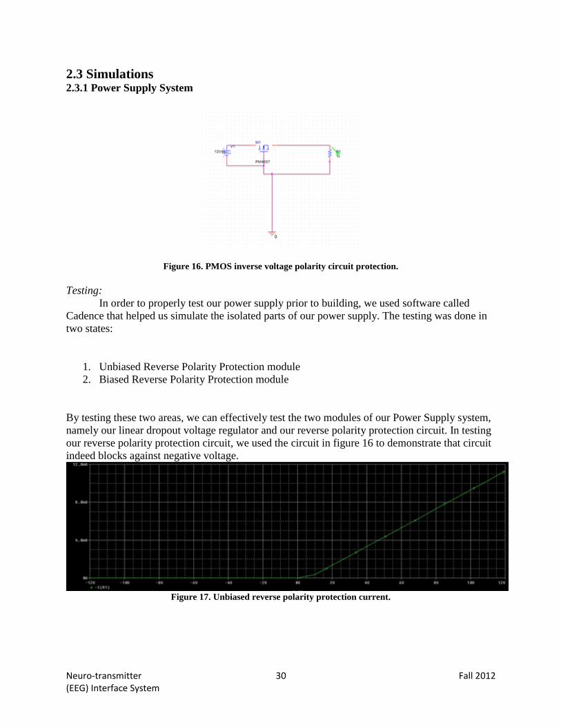
Figure 16. PMOS inverse voltage polarity circuit protection.
Testing:
In order to properly test our power supply prior to building, we used software called
Cadence that helped us simulate the isolated parts of our power supply. The testing was done in
two states:
1. Unbiased Reverse Polarity Protection module
2. Biased Reverse Polarity Protection module
By testing these two areas, we can effectively test the two modules of our Power Supply system,
namely our linear dropout voltage regulator and our reverse polarity protection circuit. In testing
our reverse polarity protection circuit, we used the circuit in figure 16 to demonstrate that circuit
indeed blocks against negative voltage.
Figure 17. Unbiased reverse polarity protection current.

Neuro-transmitter 31 Fall 2012 (EEG) Interface System
Upon close examination of the graph, we can see that there is no current before 0V, thus
confirming our hypothesis that our reverse polarity circuit works. In order to verify its efficiency,
we bias our MOSFET circuit with 30 mA. Below is the circuit that we used:
In order to properly test this circuit, we generated an IV graph that measured the steady
rectified state:
Figure 18. Biased reverse polarity protection current.
As one can see, the slope is zero, so a constant current is being emitted across a variety of
voltages confirming a steady rectified state.
2.3.2 Sensor Impedance Verification System
Testing:
In order to properly test our sensor impedance verification prior to building, we used
software called Cadence that helped us simulate two important stages of the system:
1. Current Source
2. Comparator Circuit
Neuro-transmitter 32 Fall 2012 (EEG) Interface System
By testing these two subcomponents of the block, we can show that the current in fact is
independent of the load impedance (Zskin) and that the correct LEDs light up based on the load
impedance.
The current source was simulated by replacing the skin impedance with known values that
correspond to the spectrum of impedances we plan to see.
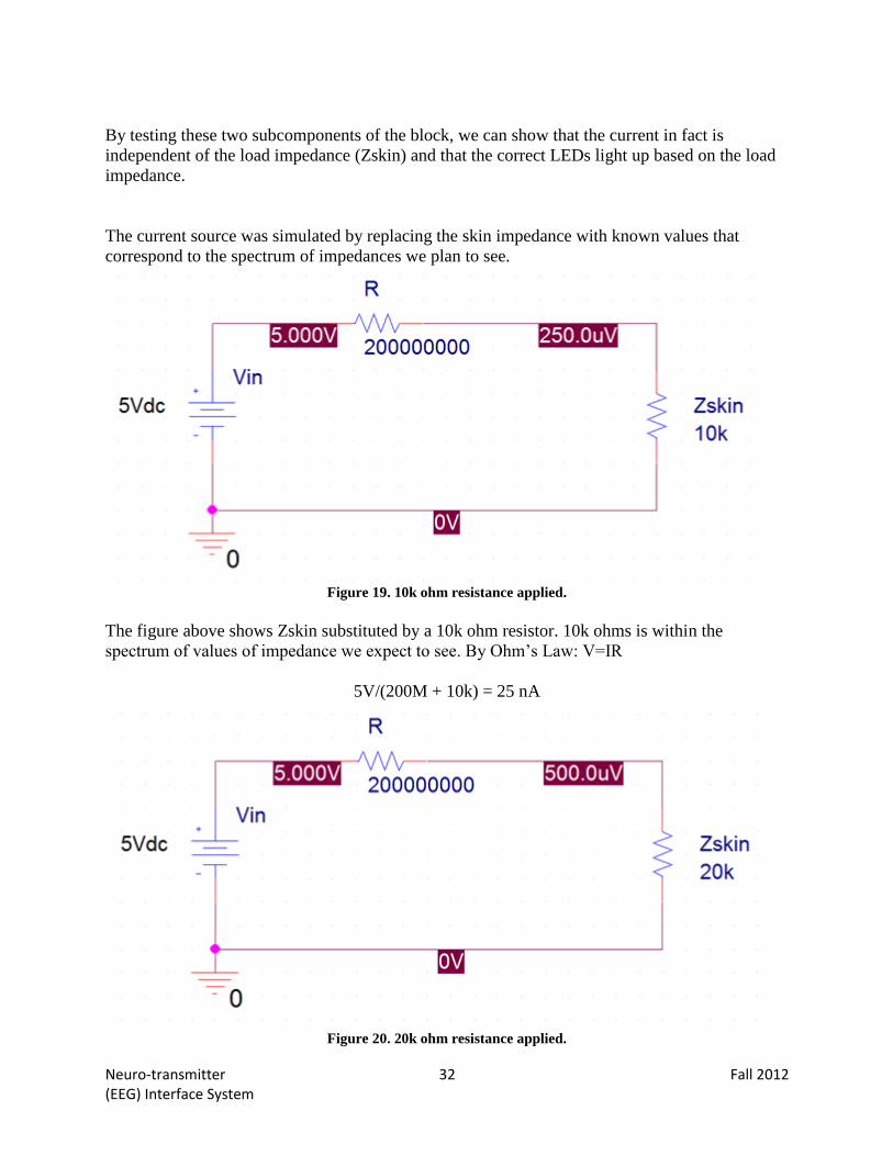
Figure 19. 10k ohm resistance applied.
The figure above shows Zskin substituted by a 10k ohm resistor. 10k ohms is within the
spectrum of values of impedance we expect to see. By Ohm’s Law: V=IR
5V/(200M + 10k) = 25 nA
Figure 20. 20k ohm resistance applied.
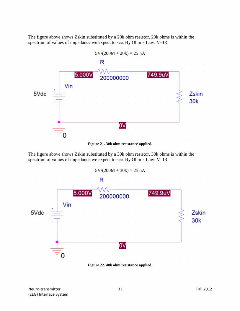
Neuro-transmitter 33 Fall 2012 (EEG) Interface System
The figure above shows Zskin substituted by a 20k ohm resistor. 20k ohms is within the
spectrum of values of impedance we expect to see. By Ohm’s Law: V=IR
5V/(200M + 20k) = 25 nA
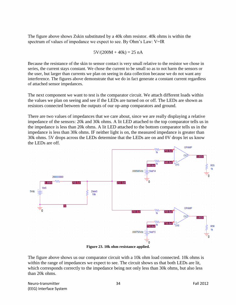
Figure 21. 30k ohm resistance applied.
The figure above shows Zskin substituted by a 30k ohm resistor. 30k ohms is within the
spectrum of values of impedance we expect to see. By Ohm’s Law: V=IR
5V/(200M + 30k) = 25 nA
Figure 22. 40k ohm resistance applied.
Neuro-transmitter 34 Fall 2012 (EEG) Interface System
The figure above shows Zskin substituted by a 40k ohm resistor. 40k ohms is within the
spectrum of values of impedance we expect to see. By Ohm’s Law: V=IR
5V/(200M + 40k) = 25 nA Because the resistance of the skin to sensor contact is very small relative to the resistor we chose in
series, the current stays constant. We chose the current to be small so as to not harm the sensors or
the user, but larger than currents we plan on seeing in data collection because we do not want any
interference. The figures above demonstrate that we do in fact generate a constant current regardless
of attached sensor impedances. The next component we want to test is the comparator circuit. We attach different loads within
the values we plan on seeing and see if the LEDs are turned on or off. The LEDs are shown as
resistors connected between the outputs of our op-amp comparators and ground.
There are two values of impedances that we care about, since we are really displaying a relative
impedance of the sensors: 20k and 30k ohms. A lit LED attached to the top comparator tells us in
the impedance is less than 20k ohms. A lit LED attached to the bottom comparator tells us in the
impedance is less than 30k ohms. IF neither light is on, the measured impedance is greater than
30k ohms. 5V drops across the LEDs determine that the LEDs are on and 0V drops let us know
the LEDs are off.
Figure 23. 10k ohm resistance applied.
The figure above shows us our comparator circuit with a 10k ohm load connected. 10k ohms is
within the range of impedances we expect to see. The circuit shows us that both LEDs are lit,
which corresponds correctly to the impedance being not only less than 30k ohms, but also less
than 20k ohms.

Neuro-transmitter 35 Fall 2012 (EEG) Interface System
Figure 24. 25k ohm resistance applied.
This time the figure above shows us our comparator circuit with a 25k ohm load connected. 25k
ohms is also within the range of impedances we expect to see. The circuit shows us that only one
of the LEDs is lit, the bottom one, which corresponds to an impedance less than 30k ohms,
which is indeed correct.
Figure 25. 40k ohm resistance applied.

Neuro-transmitter 36 Fall 2012 (EEG) Interface System
Our final simulation of the sensor impedance verification system shows us the comparator circuit
with an attached skin impedance of 40k ohms. 40k ohms is too large of a impedance to tolerate
for our circuit and will skew our data if left untouched. In this case, we want to show the user
that the impedance is too large to tolerate. We do this by leaving both LEDs unlit. Our
simulation above shows us that yes, we do actually have two LEDs left turned off, corresponding
to a skin to sensor contact impedance of 30k ohms or greater.
The overall purpose of simulation of the comparator circuitry before building the design is to
check if the logic within the circuit functions as planned. Based on our simulations, we did just
that. The current source provides a constant current that is independent of the skin-sensor
impedance, which is another term for how well the sensor is applied to the skin. The comparator
circuitry accurately determines the relative impedances of the sensors. From this we can believe
that this block is functioning as expected and proceed to assembly. 2.3.3 Amplification Simulation
In simulating the most important thing to see is that the first stage is indeed having a 100
gain from the input to the output. This is confirmed in the simulation below.

Neuro-transmitter 37 Fall 2012 (EEG) Interface System
Figure 26. 1
st stage amplifier test.
The next most important thing to check is that the total gain from the input to the final output is
indeed 10,000 as required. The simulation below confirms that this is indeed the case.
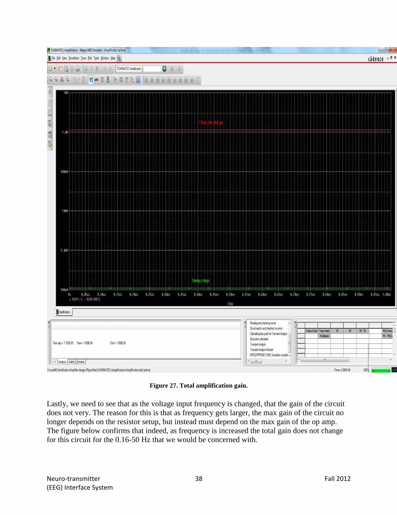
Neuro-transmitter 38 Fall 2012 (EEG) Interface System
Figure 27. Total amplification gain.
Lastly, we need to see that as the voltage input frequency is changed, that the gain of the circuit
does not very. The reason for this is that as frequency gets larger, the max gain of the circuit no
longer depends on the resistor setup, but instead must depend on the max gain of the op amp.
The figure below confirms that indeed, as frequency is increased the total gain does not change
for this circuit for the 0.16-50 Hz that we would be concerned with.

Neuro-transmitter 39 Fall 2012 (EEG) Interface System
Figure 28. Gain at various frequencies.

Neuro-transmitter 40 Fall 2012 (EEG) Interface System
2.3.4 Filter Simulation and Bode Plot
The idea of these simulations is to show why the filter system needed to be made much
more complex with more hardware than what we thought there would be at first in order to get
the needed flat band pass response that is needed. The first filter simulation shown below is the
frequency response for a simple 2nd order bandpass. This clearly shows a lot of attenuation in
the passband and very large transition bands.
Figure 29. 2
nd order bandpass.

Neuro-transmitter 41 Fall 2012 (EEG) Interface System
The next step was to take the simple bandpass filter, and take it from a second order system to a
fourth order system. The result is shorter transition bands, but also more attenuation over the
entirety of the pass band shown in the simulation below.
Figure 30. 4th
order bandpass.
Next, we simulated what would happen if we had just the fourth order lowpass in place since
filtering out the 0.16 Hz is not the most important feature of the filter. The 4th order lowpass is
shown in red below and clearly shows a shorter transition band at the cost of more attenuation in
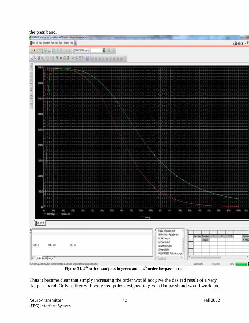
Neuro-transmitter 42 Fall 2012 (EEG) Interface System
the pass band.
Figure 31. 4
th order bandpass in green and a 4
th order lowpass in red.
Thus it became clear that simply increasing the order would not give the desired result of a very
flat pass band. Only a filter with weighted poles designed to give a flat passband would work and

Neuro-transmitter 43 Fall 2012 (EEG) Interface System
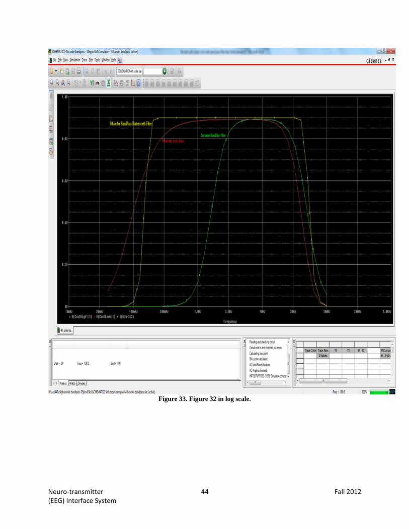
that is the very definition of the Butterworth filter. The Butterworth filter response is shown
below in yellow. Also a bode plot is included. From both it is clear to see, the 8th order band
pass Butterworth gives a very flat pass band and very sharp transitions. It is far superior to the
previous methods used with its very flat passband and very sharp transition bands.
Figure 32. Figure 31 and in yellow, an 8
th order bandpass Butterworth.
Neuro-transmitter 44 Fall 2012 (EEG) Interface System
Figure 33. Figure 32 in log scale.

Neuro-transmitter 45 Fall 2012 (EEG) Interface System
III. Verification
Tolerance Analysis For our tolerance testing, the signal amplification and filtering modules must achieve a
high precision low noise filter so that we do not corrupt our data with noise and commit it to
memory. Our tests will be checking for a 10,000 voltage gain, no current saturation, and keeping
the bandpass filter transition band and loss in signal amplitude in the pass-band to a minimum to
preserve the signal from 0.16Hz to 50Hz. Specifically we will be performing simulations using
Simulink to measure gain, and output current and to fine tune the resistor values making up the
amplifier component. Also, we will be using Simulink to simulate the specific frequencies that
the pass band occurs at for different types of filters (Butterworth, Chebychev, etc.), as-well as
showing the sensitivity to attenuation in the pass-band for these filters. Based on power
consumption, the cost, and the effectiveness of different filter types, we will decide which the
final filter to use for our system. The passband needs to be at the correct frequencies. We will
adjust the order of the filtering system based on the need to reduce noise.
IV. COST ANALYSIS
4.1 Labor
Name Hourly
Rate
Total Hours
Invested
Total=(Hourly Rate)*2.5*(Total
Hours)
Kevin Armstrong $35.00 150 $13,125
John Burton $35.00 150 $13,125
Alex Lostumbo $35.00 150 $13,125
4.2 Cost
Item Part Number Unit
Cost
Quantity Total
(USD)
Op Amps .5 slew rate LM741C 0.27 2 0.54
100k ohm resistors NTE HWCC410 2.04 2 4.08
5k ohm resistors CFR/RT13 0.50 1 0.50
1k ohm resistors RC07GF102JTR 1.19/5 7 2.38
1 ohm resistors CF-1/4WS 0.50 2 0.50

Neuro-transmitter 46 Fall 2012 (EEG) Interface System
Op Amps .4 slew rate ADA 4092 2.50 8 20.00
47k ohm resistor YJ0-365-08 1.19/5 24 5.95
100uF Capacitor 027-360 1.00 8 8.00
100nF capacitor AC1444 1.69 8 13.52
150k ohm resistors 271-1109 1.19/5 12 3.57
200M ohm resistor - 5.50 1 5.50
1:16 DeMUX HEF4514B 0.93 1 0.93
16:1 MUX 16BTC/883 7.52 2 7.52
Push Button PB-143 3.95 1 3.95
Counter Chip 74163 2.80 1 2.80
NAND logic gate 74HC21D 0.27 1 0.27
Analog Comparators LM339 2.29 2 4.58
Vref (2.5 +- .5%) TI LM4040C25 0.25 2 0.50
ADC Converter LTC2301HMS#PBF 4.01 1 4.01
Voltage Regulator LDO-7805 1.00 1 1.00
PMOS FQP47P06 2.06 1 2.06
4 D battery holder 270-396 2.19 1 2.19
4 Pack of D Batteries E95BP-4 13.00 4 13.00
Green LEDs 276-022 1.69 10 16.90
1GB SD Card SanDisk SDSDB-2048
9.99 1 9.99
Arduino Microcontroller DEV-11229 59.95 1 59.95
Purchased
enclosure 24”x24”x1/8”
- 22.33 1 22.33
PCB Board - 33.00 1 33.00
Neuro-transmitter 47 Fall 2012 (EEG) Interface System
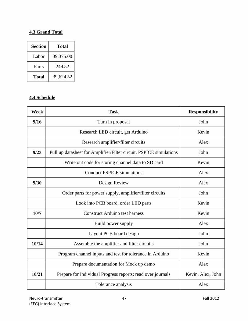
4.3 Grand Total
Section Total
Labor 39,375.00
Parts 249.52
Total 39,624.52
4.4 Schedule
Week Task Responsibility
9/16 Turn in proposal John
Research LED circuit, get Arduino Kevin
Research amplifier/filter circuits Alex
9/23 Pull up datasheet for Amplifier/Filter circuit, PSPICE simulations John
Write out code for storing channel data to SD card Kevin
Conduct PSPICE simulations Alex
9/30 Design Review Alex
Order parts for power supply, amplifier/filter circuits John
Look into PCB board, order LED parts Kevin
10/7 Construct Arduino test harness Kevin
Build power supply Alex
Layout PCB board design John
10/14 Assemble the amplifier and filter circuits John
Program channel inputs and test for tolerance in Arduino Kevin
Prepare documentation for Mock up demo Alex
10/21 Prepare for Individual Progress reports; read over journals Kevin, Alex, John
Tolerance analysis Alex

Neuro-transmitter 48 Fall 2012 (EEG) Interface System
Begin final paper(overview portion), presentation(Introductory
slides)
Kevin
10/28 Verification of specs John
Update final paper(Write-up Arduino portion) Kevin
Update presentation Alex
11/4 Mock-up Demo (individual focuses) Kevin, Alex, John
Fix remaining issues John
Completion of Modules Alex
Rehearse the A/D converter, MUX, Arduino logic flow Kevin
11/11 Check memory data is compatible with software Kevin
Edit final paper John
Edit presentation Alex
11/18 Thanksgiving break Kevin
Thanksgiving break Alex
Thanksgiving break John
11/25 Finish final draft of paper Kevin
Finish final draft of presentation Alex
Practice demo John
12/2 Demo the Arduino writing to the SD card Kevin
Demo John
Demo Alex
12/9 Tidy up the overall aesthetics of our presentation Kevin
Final Paper John
Check In Supplies Alex

Neuro-transmitter 49 Fall 2012 (EEG) Interface System
V. ENGINEERING ETHICS We will ensure that we abide to the following standards from the IEEE Code of Ethics:
1. “to accept responsibility in making decisions consistent with the safety, health and welfare of
the public, and to disclose promptly factors that might endanger the public or the environment.” Our group is working toward creating a safe and affordable EEG that would be conducive with
current health and safety standards. Our final device depends on the safety of the individual,
since the data itself is useless without the individual trusting the device.
Our project contains an impedance reading system that sends current through the sensors applied
to the heads of our users. Safety is crucial to a device that is interfacing with the human brain.
Limitations on current are essential to the health of the user. There are serious consequences
associated with ignoring the amount of current sent through the human body, which include pain,
paralysis, and possible death. The health and safety of our users is of the utmost importance.
5. “to improve the understanding of technology; its appropriate application, and potential
consequences.”
We are bound by this ethical code to act accordingly in society. We must showcase the power
that lies behind advancements in technology, but avoid ambiguity at all costs about the potential
consequences of such new inventions. Our project will lay new ground in the field of
neurological research, but all of our actions have unanticipated and unforeseeable consequences. 6. “to maintain and improve our technical competence and to undertake technological tasks for
others only if qualified by training or experience, or after full disclosure of pertinent limitations.” Although we are not officially certified with a medical or engineering license, we are closely
working with those that have earned at least their Bachelor's of Science (Ryan May), while Prof.
Andrew Singer and Kyle Matthewson both have achieved a doctoral status in the field of
engineering and neuroscience, respectively.
7. “to seek, accept, and offer honest criticism of technical work, to acknowledge and correct
errors, and to credit properly the contributions of others.” Ryan May and other instructors/professors are offering their wisdom to create the most efficient
EEG we can with our limited budget. Kyle Matthewson, a post-doctoral student studying
neuroscience at the Beckman Institute, serves as our group’s point-of-contact in understanding
how the EEG device properly functions. Working together as a team, we will critique each
other’s work to produce the best possible product. 9. “to avoid injuring others, their property, reputation, or employment by false or malicious
action.”
Focusing on safety, we want to make certain that our product does not harm anyone involved.
We must constantly reiterate that the safety of our subjects will be the primary goal throughout

Neuro-transmitter 50 Fall 2012 (EEG) Interface System
this process. We also plan on ensuring the safety of the sensor cap we plan on using, which is in
fact, not our personal property.
VI. Resources:
"Arduino - SD." Arduino - SD. Scott Fitzgerald, 11 Nov. 2011. Web. 01 Oct. 2012.
<http://arduino.cc/en/Reference/SD>.
"P-FET Reverse Voltage Polarity Protection Tutorial." YouTube. YouTube, 01 Dec. 2011.
Web. 01 Oct. 2012. <http://www.youtube.com/watch?v=IrB-FPcv1Dc>.
"Analog Filter Design Demystified." - Tutorial. N.p., n.d. Web. 02 Oct. 2012.
<http://www.maximintegrated.com/app-notes/index.mvp/id/1795>.
"The ModularEEG Design." The ModularEEG Design. N.p., n.d. Web. 26 Sept. 2012.
<http://openeeg.sourceforge.net/doc/modeeg/modeeg_design.html>.