NEC 79VR5000 RISC MICROPROCESSOR - si
56
Construction Analysis NEC 79VR5000 RISC Microprocessor Report Number: SCA 9711-567 ® S e r v i n g t h e G l o b a l S e m i c o n d u c t o r I n d u s t r y S i n c e 1 9 6 4 17350 N. Hartford Drive Scottsdale, AZ 85255 Phone: 602-515-9780 Fax: 602-515-9781 e-mail: [email protected] Internet: http://www.ice-corp.com
Transcript of NEC 79VR5000 RISC MICROPROCESSOR - si
Construction Analysis
NEC 79VR5000 RISC Microprocessor
Report Number: SCA 9711-567
®
Serv
ing
the
Global Semiconductor Industry
Since1964
17350 N. Hartford DriveScottsdale, AZ 85255Phone: 602-515-9780Fax: 602-515-9781
e-mail: [email protected]: http://www.ice-corp.com
- i -
INDEX TO TEXT
TITLE PAGE
INTRODUCTION 1
MAJOR FINDINGS 1
TECHNOLOGY DESCRIPTION
Assembly 2
Die process and design 2 - 3
ANALYSIS RESULTS I
Assembly 4
ANALYSIS RESULTS II
Die Process 5 - 7
TABLES
Procedure 8
Overall Quality Evaluation 9
Package Markings 10
Wirebond Strength 10
Die Material Analysis (WDX) 10
Horizontal Dimensions 11
Vertical Dimensions 12
- 1 -
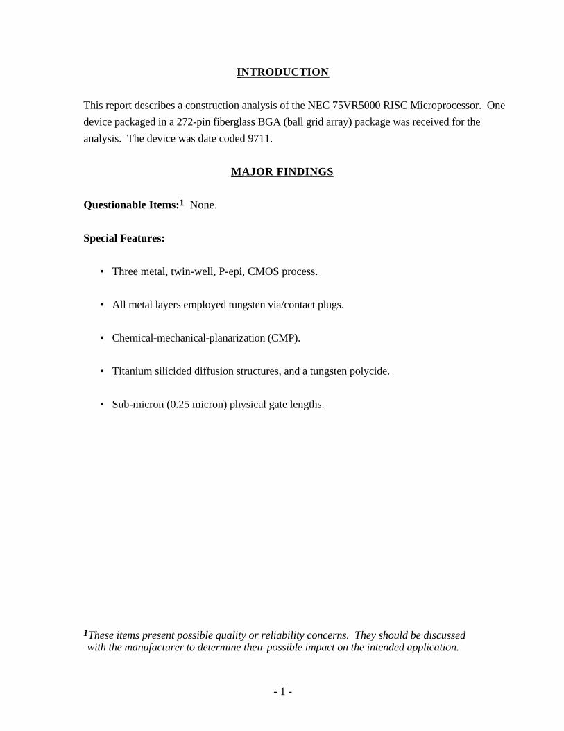
INTRODUCTION
This report describes a construction analysis of the NEC 75VR5000 RISC Microprocessor. One
device packaged in a 272-pin fiberglass BGA (ball grid array) package was received for the
analysis. The device was date coded 9711.
MAJOR FINDINGS
Questionable Items:1 None.
Special Features:
• Three metal, twin-well, P-epi, CMOS process.
• All metal layers employed tungsten via/contact plugs.
• Chemical-mechanical-planarization (CMP).
• Titanium silicided diffusion structures, and a tungsten polycide.
• Sub-micron (0.25 micron) physical gate lengths.
1These items present possible quality or reliability concerns. They should be discussedwith the manufacturer to determine their possible impact on the intended application.
- 2 -
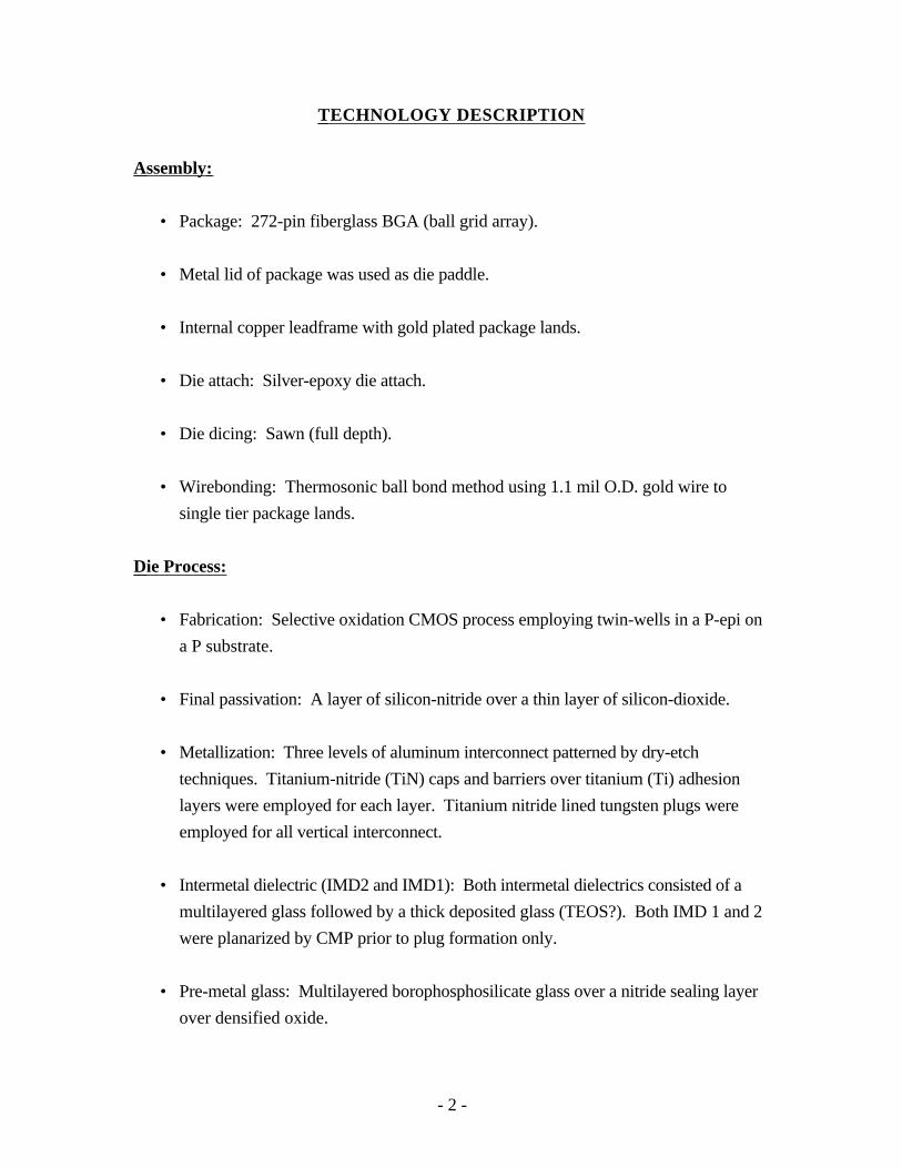
TECHNOLOGY DESCRIPTION
Assembly:
• Package: 272-pin fiberglass BGA (ball grid array).
• Metal lid of package was used as die paddle.
• Internal copper leadframe with gold plated package lands.
• Die attach: Silver-epoxy die attach.
• Die dicing: Sawn (full depth).
• Wirebonding: Thermosonic ball bond method using 1.1 mil O.D. gold wire to
single tier package lands.
Die Process:
• Fabrication: Selective oxidation CMOS process employing twin-wells in a P-epi on
a P substrate.
• Final passivation: A layer of silicon-nitride over a thin layer of silicon-dioxide.
• Metallization: Three levels of aluminum interconnect patterned by dry-etch
techniques. Titanium-nitride (TiN) caps and barriers over titanium (Ti) adhesion
layers were employed for each layer. Titanium nitride lined tungsten plugs were
employed for all vertical interconnect.
• Intermetal dielectric (IMD2 and IMD1): Both intermetal dielectrics consisted of a
multilayered glass followed by a thick deposited glass (TEOS?). Both IMD 1 and 2
were planarized by CMP prior to plug formation only.
• Pre-metal glass: Multilayered borophosphosilicate glass over a nitride sealing layer
over densified oxide.
- 3 -
TECHNOLOGY DESCRIPTION (continued)
• Polysilicon: Polycide (poly and tungsten silicide) formed all gates on the die
including the select and storage gates in the Cache memory arrays.
• Diffusions: LDD process with oxide sidewall spacers left in place, and implanted
N+ and P+ sources/drains with a titanium silicide on top. Twin-wells were used in a
P-epi on a P substrate.
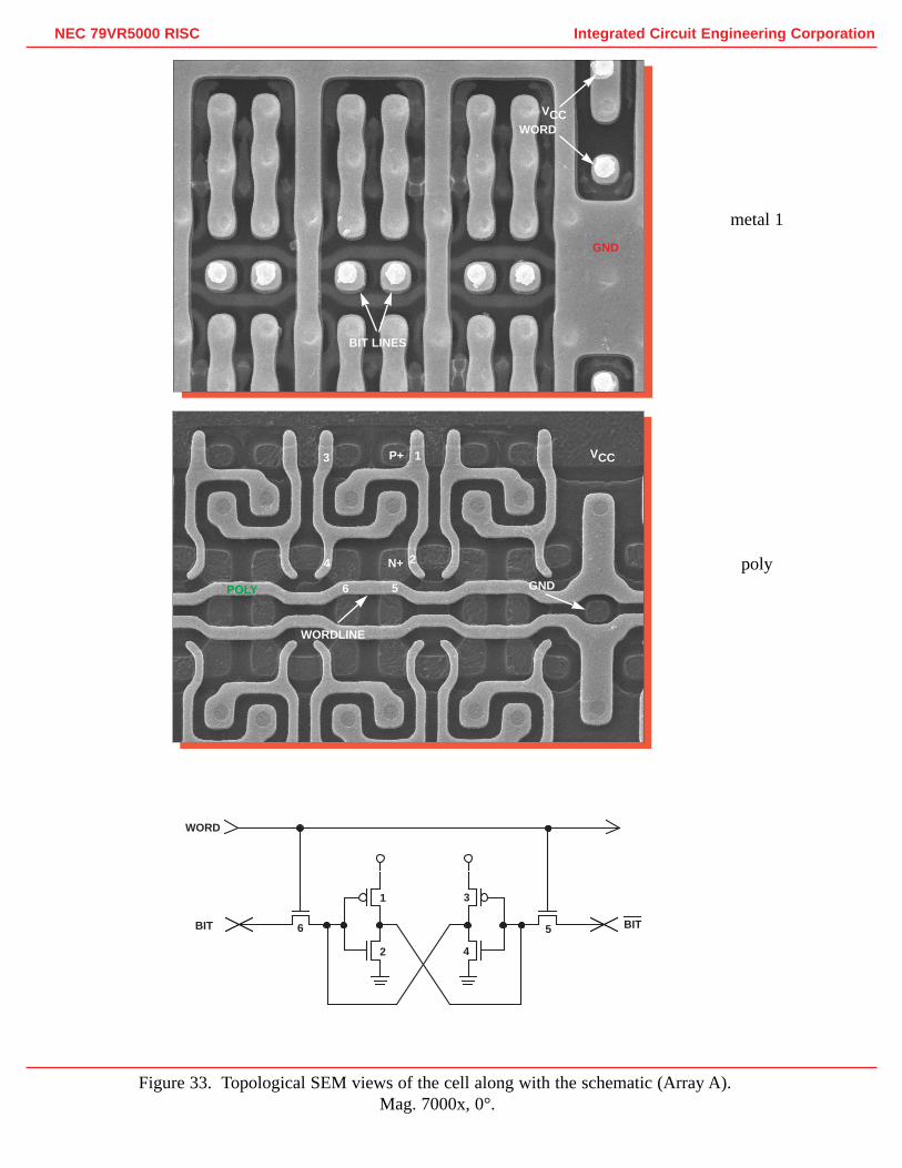
• Memory cells: Cache SRAM cell arrays were employed on this device. Metal 2
formed "piggyback" word lines, the bit lines and distributed Vcc (via metal 1).
Polycide formed the word lines, select and storage gates.
• Fuses: No redundancy fuses were found.
- 4 -
ANALYSIS RESULTS I
Assembly: Figures 1 - 5
Questionable Items:1 None.
Design Features:
• The metal lid of the package was employed as a paddle to mount the die.
General Items:
• 272-pin fiberglass BGA (ball grid array). The die was connected to the package lands by
wirebonds.
• Overall package quality: Normal. The Ball Grid Array package included a multilayer
fiberglass board with solder balls that were evenly spaced and the die was sealed with a
black encapsulant on the underside of the package. No voids or problems were noted with
the package.
• Die attach: The die was attached to the metal lid/paddle using a silver epoxy die attach of
good quality.
• Die dicing: Die separation was by sawing with normal quality workmanship.
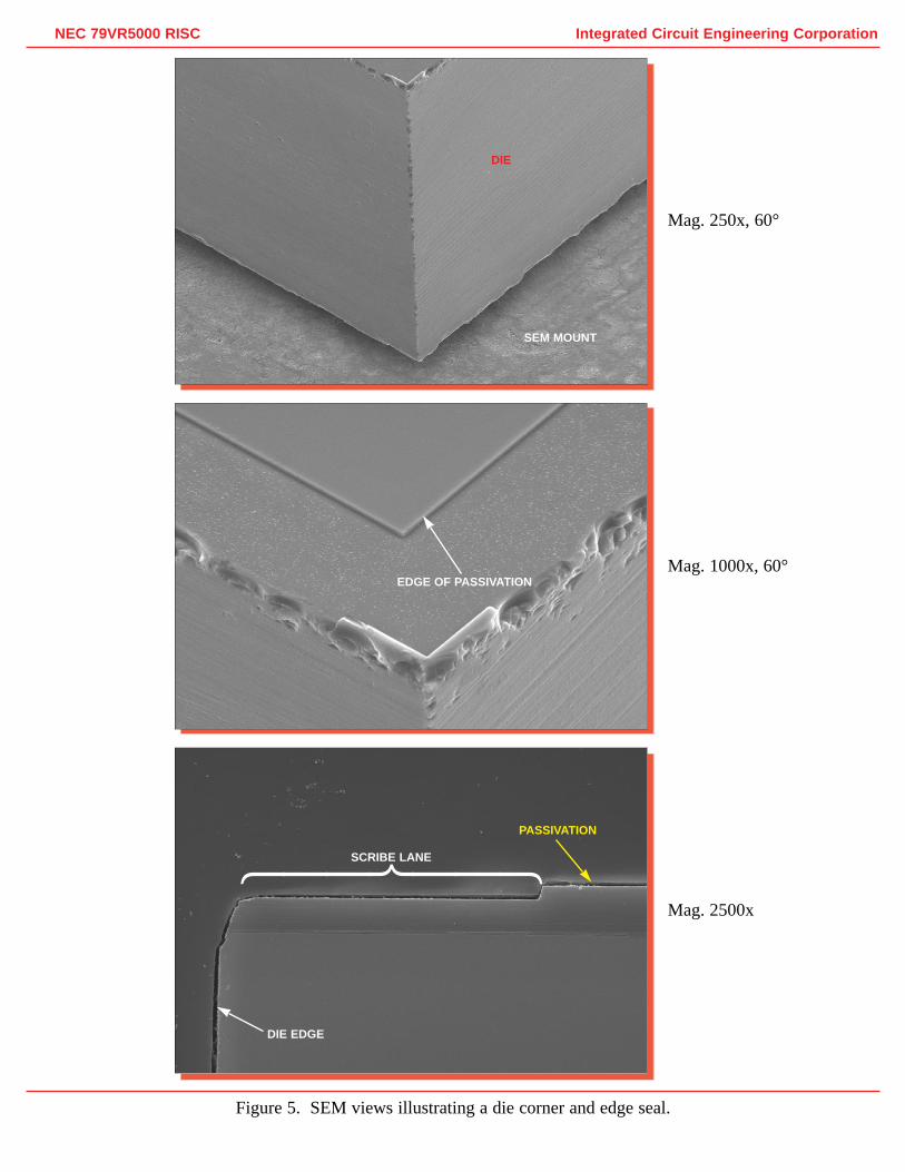
• Edge seal: Good. The passivation extended to the scribe lane to seal off the metallization.
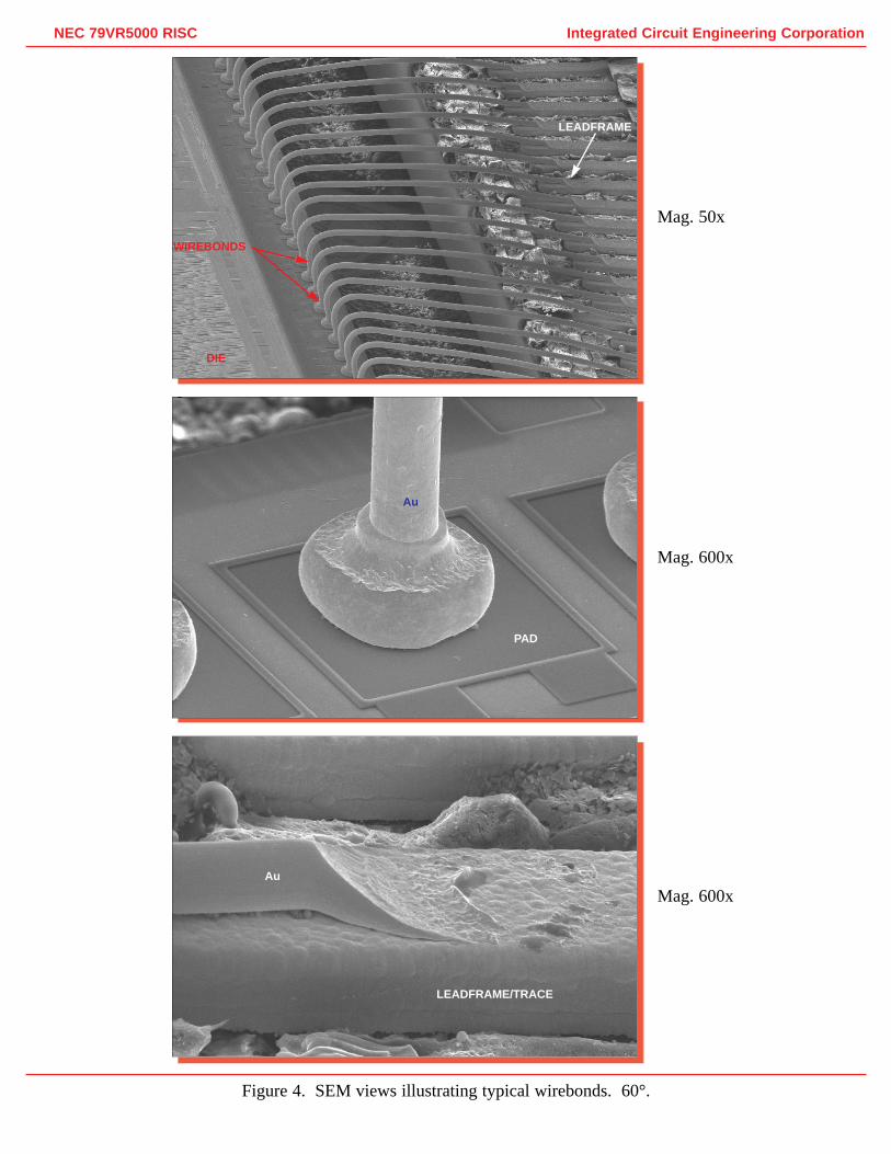
• Wirebonding: Single tier wirebonding employing a thermosonic ball bond method using 1.1
mil O.D gold wire. Wire spacing and clearance were adequate at the die edge. The die was
mounted low enough in the cavity of the fiberglass board to assist with bonding wire
clearance. All wires had normal bond pull strengths (see page 12).
1These items present possible quality or reliability concerns. They should be discussedwith the manufacturer to determine their possible impact on the intended application.
- 5 -
ANALYSIS RESULTS II
Die Process: Figures 6 - 37
Questionable Items:1 None.
Special Features:
• Three metal, twin-well, P-epi, CMOS process.
• All metal layers employed tungsten via/contact plugs.
• Chemical-mechanical-planarization (CMP).
• Titanium silicided diffusion structures, and tungsten silicide on poly.
• Sub-micron (0.25 micron) physical gate lengths.
General Items:
• Fabrication process: Selective oxidation CMOS process employing twin-wells in a
P-epi on a P substrate.
• Process Implementation: No areas of concern were found. Active area die layout
was clean. Alignment/registration was good at all levels and no damage or
contamination was found.
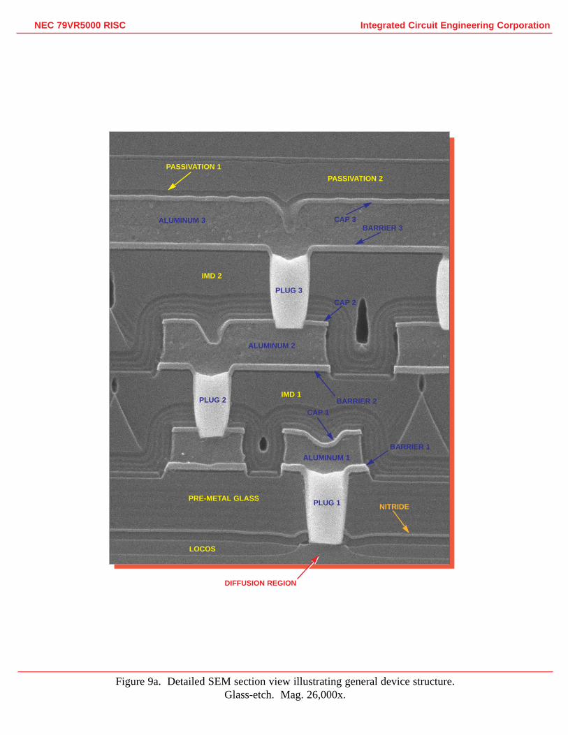
• Final Passivation: A layer of silicon-nitride over a thin layer of silicon-dioxide was
employed. Integrity tests indicated defect-free passivation. Edge seal was good as
the passivation extended into the scribe lane.
1These items present possible quality or reliability concerns. They should be discussedwith the manufacturer to determine their possible impact on the intended application.

- 6 -
ANALYSIS RESULTS II (continued)
• Metallization: Three levels of aluminum interconnect patterned by dry-etch
techniques. Titanium-nitride (TiN) caps and barriers over titanium (Ti) adhesion
layers were employed for each layer. Tungsten plugs lined underneath with
titanium-nitride were used for all vertical interconnect. Plugs had not been subjected
to CMP so were not particularly well planarized.
• Metal patterning: Metal layers were defined by dry-etch techniques. Definition was
normal for both layers, and no defects were found.
• Metal defects: No voiding or notching of the metals was found.
• Metal step coverage: No excessive metal thinning was present due to the use of
tungsten plugs; however, metal 2 and metal 3 aluminum thinned up to 50 percent at
via edges.
• Vias and contacts: Via and contact cuts were dry-etched after the dielectric layers
were planarized. Slight overetching of the M3 and M2 vias was used to penetrate the
cap metal. This appeared well controlled.
• Intermetal dielectrics (IMD2 and IMD1): Both intermetal dielectrics consisted of a
multilayered glass followed by another layer of deposited glass (TEOS?). As
mentioned, both dielectrics were well planarized by CMP.
• Pre-metal glass: The dielectric between metal 1 and polysilicon consisted of a
borophosphosilicate glass over a nitride sealing layer over grown oxide. The top of
this dielectric was also planarized by CMP. No problems were found in any of the
dielectric layers.
• Polysilicon: Polycide (poly and tungsten silicide) formed all gates on the die
including the select and storage gates in the Cache memory array. Oxide sidewall
spacers were left in place although they appeared to have been backetched some.
• Isolation: Heavily backetched local oxide (LOCOS). No problems were present at
the birdsbeaks. A step was present indicating a twin-wells process.
- 7 -
ANALYSIS RESULTS II (continued)
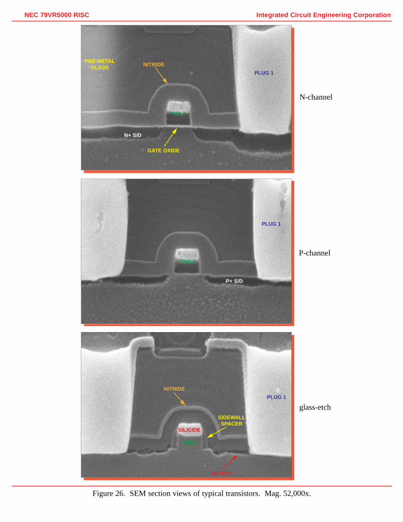
• Diffusions: LDD process with oxide sidewall spacers left in place. Implanted N+
and P+ source/drains employed a titanium silicide process, although poly used a
tungsten silicide. Definition was normal and no problems were present.
• Wells: Twin-wells in a P-epi on a P substrate. No problems were apparent.
• Memory cells: Cache SRAM cell arrays were employed on this device. Metal 2
formed "piggyback" word lines, the bit lines, and distributed Vcc (via metal 1).
Polycide formed the word lines and storage gates. Cell pitch was 4.35 x 6.9
microns (30 microns2).

- 8 -
PROCEDURE
The devices were subjected to the following analysis procedures:
External inspection
X-ray
Decapsulation
Internal optical inspection
SEM of assembly features
Wirepull tests
Passivation integrity tests
Passivation removal and inspect metal 3
Aluminum 3 removal
Delayer to metal 2 and inspect
Aluminum 2 removal
Delayer to metal 1 and inspect
Aluminum 1 removal
Delayer to poly/substrate and inspect poly structures and die surface
Die material analysis
Die sectioning (90° for SEM)*
Measure horizontal dimensions
Measure vertical dimensions
*Delineation of cross-sections is by silicon etch unless otherwise indicated.
- 9 -
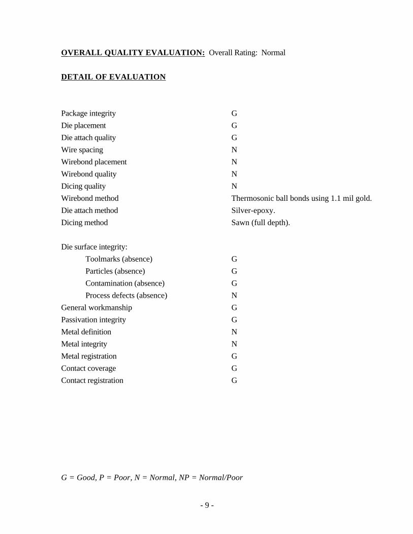
OVERALL QUALITY EVALUATION: Overall Rating: Normal
DETAIL OF EVALUATION
Package integrity G
Die placement G
Die attach quality G
Wire spacing N
Wirebond placement N
Wirebond quality N
Dicing quality N
Wirebond method Thermosonic ball bonds using 1.1 mil gold.
Die attach method Silver-epoxy.
Dicing method Sawn (full depth).
Die surface integrity:
Toolmarks (absence) G
Particles (absence) G
Contamination (absence) G
Process defects (absence) N
General workmanship G
Passivation integrity G
Metal definition N
Metal integrity N
Metal registration G
Contact coverage G
Contact registration G
G = Good, P = Poor, N = Normal, NP = Normal/Poor
- 10 -
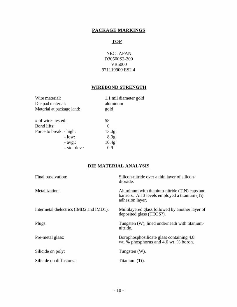
PACKAGE MARKINGS
TOP
NEC JAPAND30500S2-200
VR5000971119900 ES2.4
WIREBOND STRENGTH
Wire material: 1.1 mil diameter goldDie pad material: aluminumMaterial at package land: gold
# of wires tested: 58Bond lifts: 0Force to break - high: 13.0g
- low: 8.0g - avg.: 10.4g - std. dev.: 0.9
DIE MATERIAL ANALYSIS
Final passivation: Silicon-nitride over a thin layer of silicon-dioxide.
Metallization: Aluminum with titanium-nitride (TiN) caps and barriers. All 3 levels employed a titanium (Ti) adhesion layer.
Intermetal dielectrics (IMD2 and IMD1): Multilayered glass followed by another layer of deposited glass (TEOS?).
Plugs: Tungsten (W), lined underneath with titanium-nitride.
Pre-metal glass: Borophosphosilicate glass containing 4.8 wt. % phosphorus and 4.0 wt .% boron.
Silicide on poly: Tungsten (W).
Silicide on diffusions: Titanium (Ti).
- 11 -
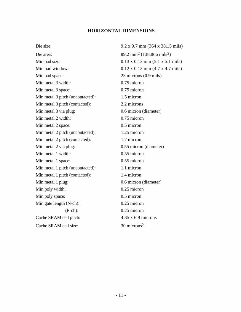
HORIZONTAL DIMENSIONS
Die size: 9.2 x 9.7 mm (364 x 381.5 mils)
Die area: 89.2 mm2 (138,866 mils2)
Min pad size: 0.13 x 0.13 mm (5.1 x 5.1 mils)
Min pad window: 0.12 x 0.12 mm (4.7 x 4.7 mils)
Min pad space: 23 microns (0.9 mils)
Min metal 3 width: 0.75 micron
Min metal 3 space: 0.75 micron
Min metal 3 pitch (uncontacted): 1.5 micron
Min metal 3 pitch (contacted): 2.2 microns
Min metal 3 via plug: 0.6 micron (diameter)
Min metal 2 width: 0.75 micron
Min metal 2 space: 0.5 micron
Min metal 2 pitch (uncontacted): 1.25 micron
Min metal 2 pitch (contacted): 1.7 micron
Min metal 2 via plug: 0.55 micron (diameter)
Min metal 1 width: 0.55 micron
Min metal 1 space: 0.55 micron
Min metal 1 pitch (uncontacted): 1.1 micron
Min metal 1 pitch (contacted): 1.4 micron
Min metal 1 plug: 0.6 micron (diameter)
Min poly width: 0.25 micron
Min poly space: 0.5 micron
Min gate length (N-ch): 0.25 micron
(P-ch): 0.25 micron
Cache SRAM cell pitch: 4.35 x 6.9 microns
Cache SRAM cell size: 30 microns2
- 12 -
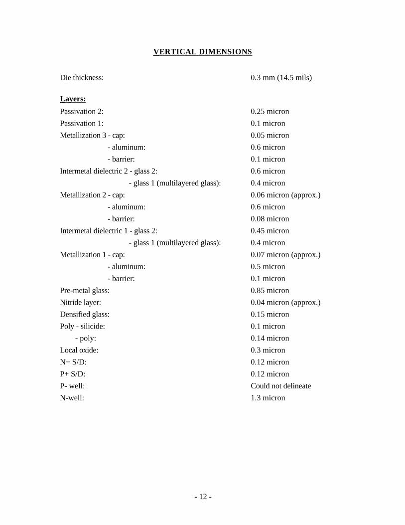
VERTICAL DIMENSIONS
Die thickness: 0.3 mm (14.5 mils)
Layers:
Passivation 2: 0.25 micron
Passivation 1: 0.1 micron
Metallization 3 - cap: 0.05 micron
- aluminum: 0.6 micron
- barrier: 0.1 micron
Intermetal dielectric 2 - glass 2: 0.6 micron
- glass 1 (multilayered glass): 0.4 micron
Metallization 2 - cap: 0.06 micron (approx.)
- aluminum: 0.6 micron
- barrier: 0.08 micron
Intermetal dielectric 1 - glass 2: 0.45 micron
- glass 1 (multilayered glass): 0.4 micron
Metallization 1 - cap: 0.07 micron (approx.)
- aluminum: 0.5 micron
- barrier: 0.1 micron
Pre-metal glass: 0.85 micron
Nitride layer: 0.04 micron (approx.)
Densified glass: 0.15 micron
Poly - silicide: 0.1 micron
- poly: 0.14 micron
Local oxide: 0.3 micron
N+ S/D: 0.12 micron
P+ S/D: 0.12 micron
P- well: Could not delineate
N-well: 1.3 micron

- ii -
INDEX TO FIGURES
PACKAGE AND ASSEMBLY Figures 1 - 5
DIE LAYOUT AND IDENTIFICATION Figures 6 - 8
PHYSICAL DIE STRUCTURES Figures 9 - 37
COLOR PROCESS DRAWING Figure 29
MEMORY CELL STRUCTURES Figure 30 - 35
GENERAL CIRCUIT LAYOUT Figure 36
TYPICAL INPUT/OUTPUT LAYOUT Figure 37
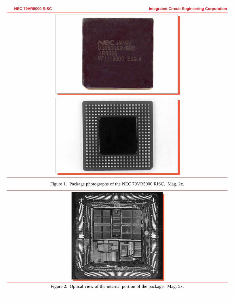
Figure 1. Package photographs of the NEC 79VR5000 RISC. Mag. 2x.
Integrated Circuit Engineering CorporationNEC 79VR5000 RISC
Figure 2. Optical view of the internal portion of the package. Mag. 5x.
Integrated Circuit Engineering CorporationNEC 79VR5000 RISC
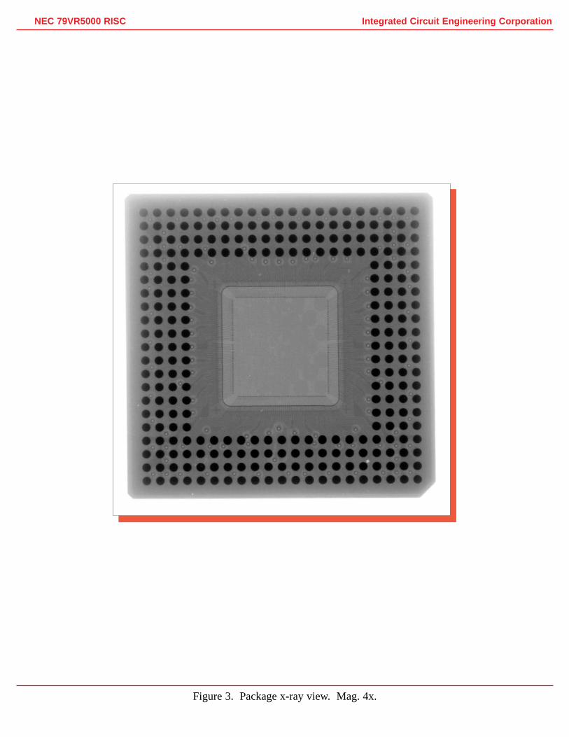
Figure 3. Package x-ray view. Mag. 4x.
Mag. 50x
Mag. 600x
Mag. 600x
Integrated Circuit Engineering CorporationNEC 79VR5000 RISC
Figure 4. SEM views illustrating typical wirebonds. 60°.
WIREBONDS
DIE
Au
PAD
LEADFRAME
Au
LEADFRAME/TRACE
Mag. 250x, 60°
Mag. 1000x, 60°
Mag. 2500x
Integrated Circuit Engineering CorporationNEC 79VR5000 RISC
Figure 5. SEM views illustrating a die corner and edge seal.
DIE
SEM MOUNT
EDGE OF PASSIVATION
11444422444433 SCRIBE LANE
PASSIVATION
DIE EDGE
Integrated Circuit Engineering CorporationNEC 79VR5000 RISC
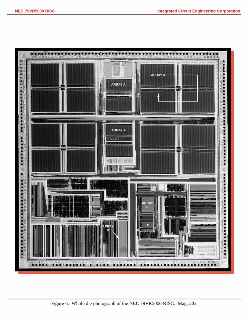
Figure 6. Whole die photograph of the NEC79VR5000 RISC. Mag. 20x.
ARRAY A
ARRAY A
ARRAY A
ARRAYC
CARRAYB
Integrated Circuit Engineering CorporationNEC 79VR5000 RISC
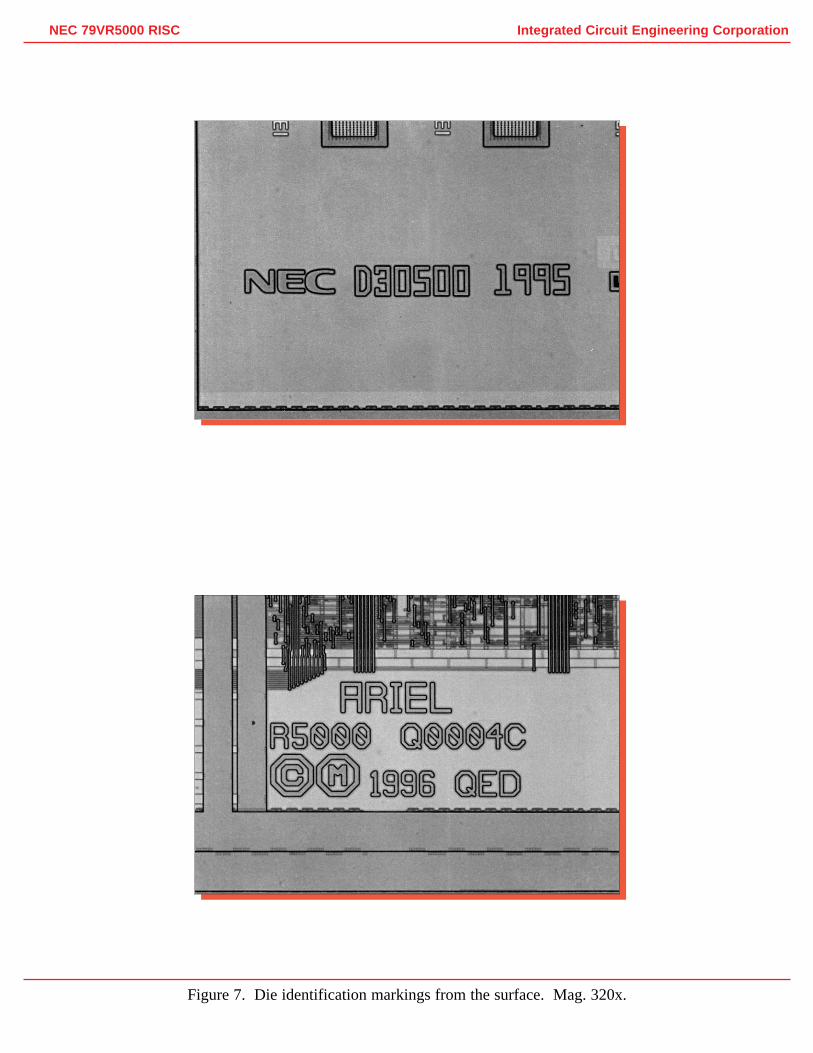
Figure 7. Die identification markings from the surface. Mag. 320x.
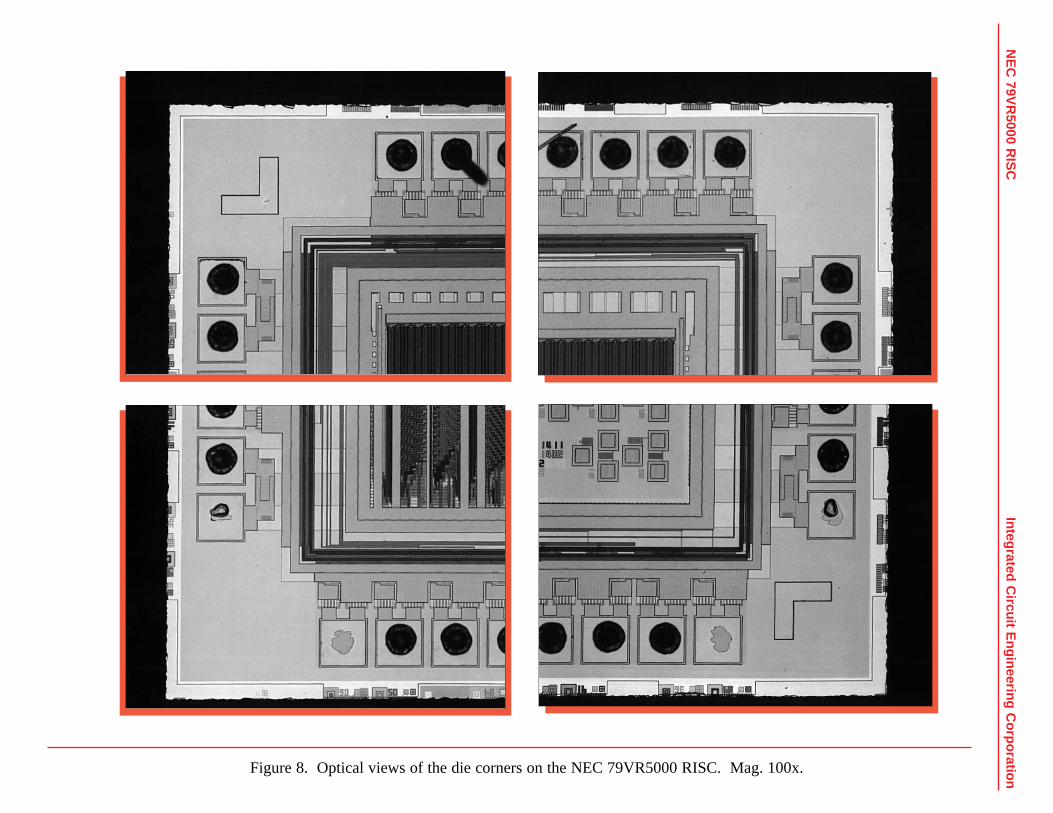
Figure 8. Optical views of the die corners on the NEC 79VR5000 RISC. Mag. 100x.
Integrated Circuit E
ngineering Corporation
NE
C 79V
R5000 R
ISC
Integrated Circuit Engineering CorporationNEC 79VR5000 RISC
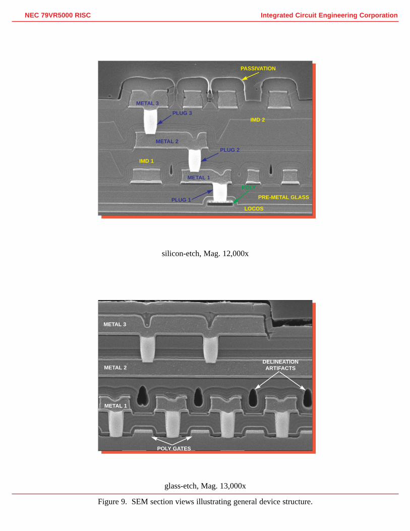
glass-etch, Mag. 13,000x
silicon-etch, Mag. 12,000x
Figure 9. SEM section views illustrating general device structure.
METAL 3
PASSIVATION
PLUG 3
METAL 2
IMD 2
IMD 1
PLUG 2
METAL 1
POLY
PLUG 1 PRE-METAL GLASS
LOCOS
METAL 3
METAL 2
METAL 1
POLY GATES
DELINEATIONARTIFACTS
Integrated Circuit Engineering CorporationNEC 79VR5000 RISC
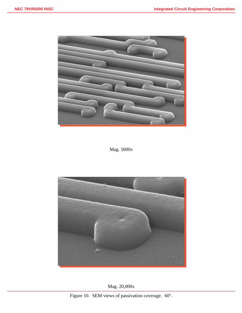
Mag. 20,000x
Mag. 5000x
Figure 10. SEM views of passivation coverage. 60°.
Integrated Circuit Engineering CorporationNEC 79VR5000 RISC
Figure 9a. Detailed SEM section view illustrating general device structure. Glass-etch. Mag. 26,000x.
PASSIVATION 1
PASSIVATION 2
ALUMINUM 3 CAP 3BARRIER 3
IMD 2
PLUG 3
CAP 2
ALUMINUM 2
BARRIER 2PLUG 2IMD 1
CAP 1
ALUMINUM 1BARRIER 1
PRE-METAL GLASS PLUG 1 NITRIDE
LOCOS
DIFFUSION REGION
Integrated Circuit Engineering CorporationNEC 79VR5000 RISC
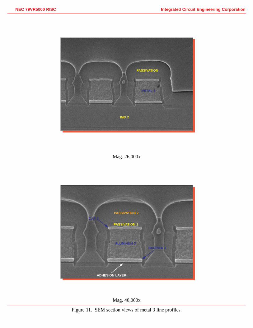
Mag. 40,000x
Mag. 26,000x
Figure 11. SEM section views of metal 3 line profiles.
PASSIVATION
METAL 3
IMD 2
PASSIVATION 2
PASSIVATION 1
CAP 3
ALUMINUM 3BARRIER 3
ADHESION LAYER
Mag. 2000x
Mag. 3200x
Mag. 13,000x
Integrated Circuit Engineering CorporationNEC 79VR5000 RISC
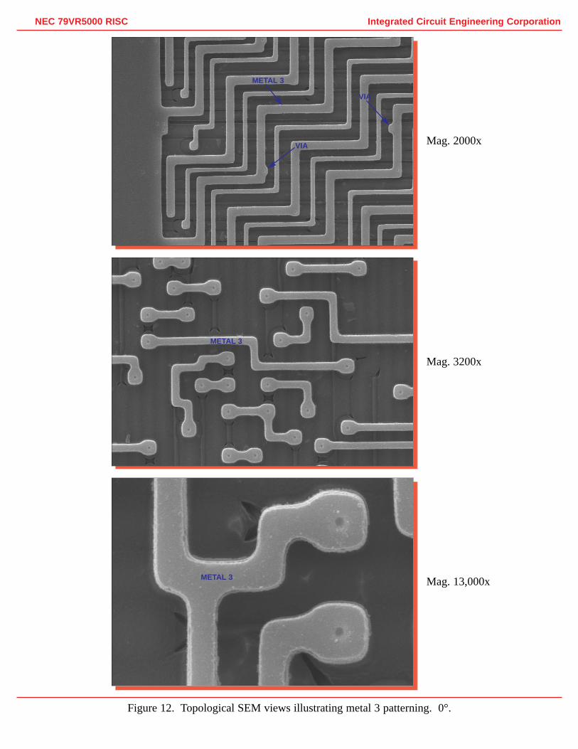
Figure 12. Topological SEM views illustrating metal 3 patterning. 0°.
METAL 3
VIA
VIA
METAL 3
METAL 3
Integrated Circuit Engineering CorporationNEC 79VR5000 RISC
Mag. 10,000x
Mag. 5000x
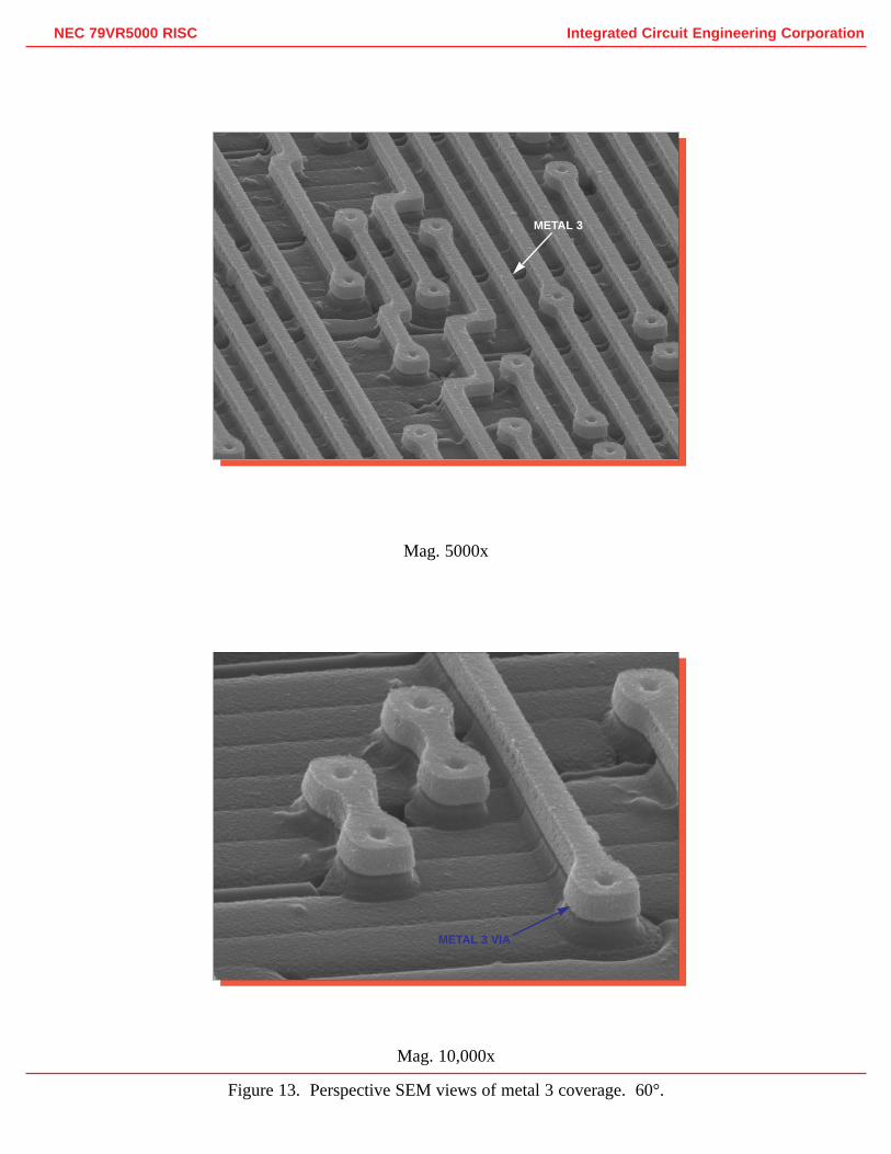
Figure 13. Perspective SEM views of metal 3 coverage. 60°.
METAL 3
METAL 3 VIA
Integrated Circuit Engineering CorporationNEC 79VR5000 RISC
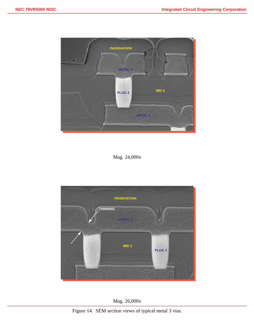
Mag. 26,000x
Mag. 24,000x
Figure 14. SEM section views of typical metal 3 vias.
PASSIVATION
METAL 3
PLUG 3IMD 2
METAL 2
METAL 3
PASSIVATION
IMD 2PLUG 3
THINNING
Integrated Circuit Engineering CorporationNEC 79VR5000 RISC
Mag. 40,000x
Mag. 26,000x
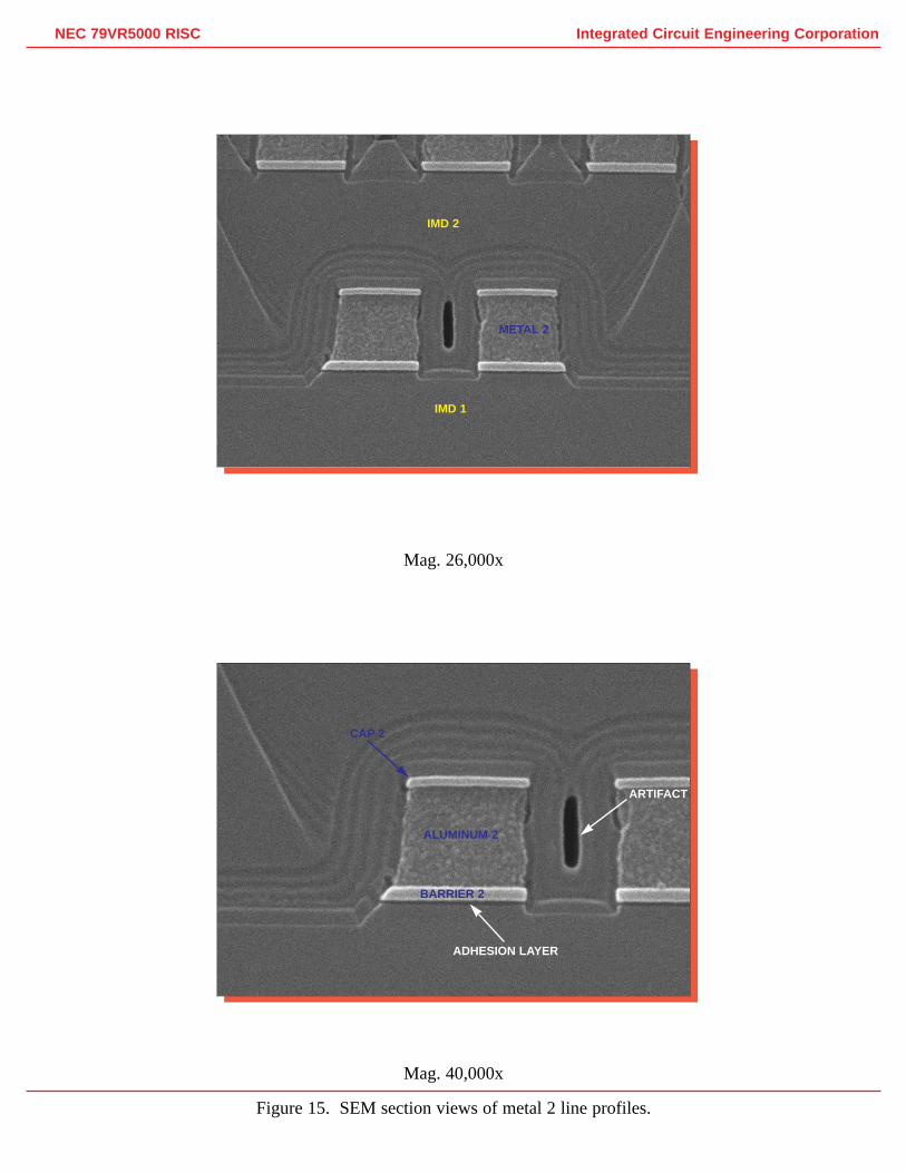
Figure 15. SEM section views of metal 2 line profiles.
IMD 2
METAL 2
IMD 1
CAP 2
ALUMINUM 2
BARRIER 2
ADHESION LAYER
ARTIFACT
Mag. 2500x
Mag. 5000x
Mag. 10,000x
Integrated Circuit Engineering CorporationNEC 79VR5000 RISC
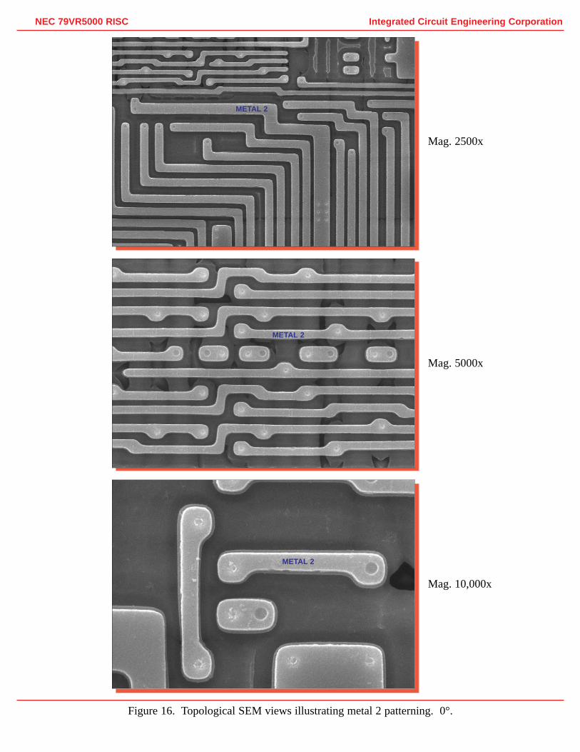
Figure 16. Topological SEM views illustrating metal 2 patterning. 0°.
METAL 2
METAL 2
METAL 2
Mag. 5000x
Mag. 5000x
Mag. 16,000x
Integrated Circuit Engineering CorporationNEC 79VR5000 RISC
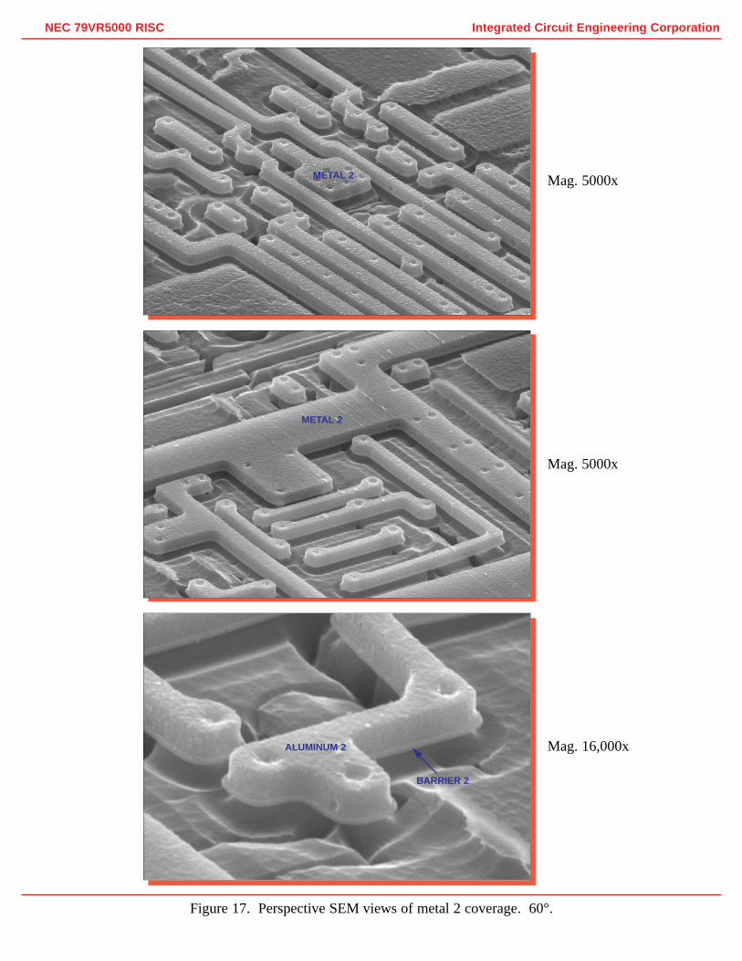
Figure 17. Perspective SEMviews of metal 2 coverage. 60°.
METAL 2
METAL 2
ALUMINUM 2
BARRIER 2

Integrated Circuit Engineering CorporationNEC 79VR5000 RISC
Mag. 40,000x, 60°
Mag. 30,000x
Figure 18. SEM views of a metal 2 via and plug.
METAL 2
PLUG 2
PLUG 2
METAL 1
METAL 1
Integrated Circuit Engineering CorporationNEC 79VR5000 RISC
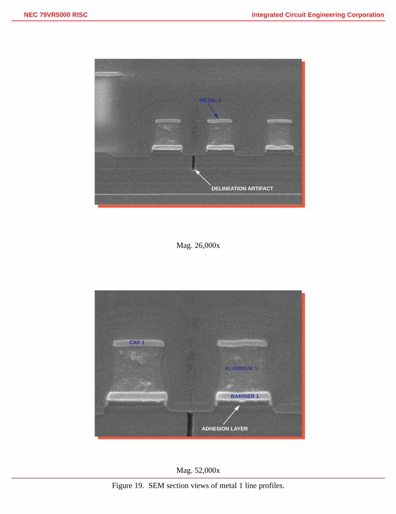
Mag. 52,000x
Mag. 26,000x
Figure 19. SEM section views of metal 1 line profiles.
METAL 1
DELINEATION ARTIFACT
CAP 1
ALUMINUM 1
BARRIER 1
ADHESION LAYER
Mag. 3500x
Mag. 6500x
Mag. 8000x
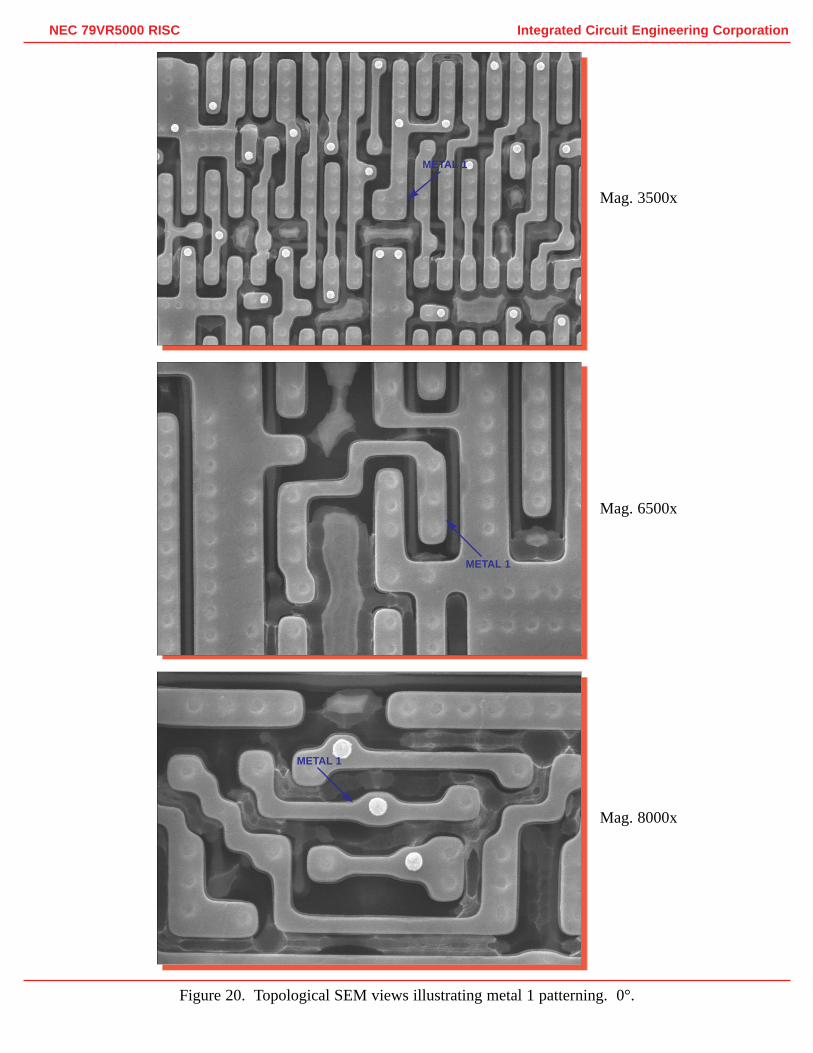
Integrated Circuit Engineering CorporationNEC 79VR5000 RISC
Figure 20. Topological SEM views illustrating metal 1 patterning. 0°.
METAL 1
METAL 1
METAL 1
Mag. 4500x
Mag. 18,000x
Mag. 18,000x
Integrated Circuit Engineering CorporationNEC 79VR5000 RISC
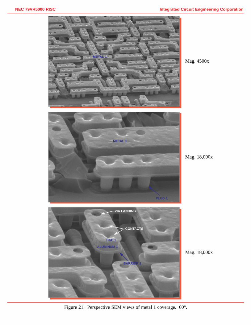
Figure 21. Perspective SEM views of metal 1 coverage. 60°.
METAL 1
METAL 1
PLUG 1
ALUMINUM 1
VIA LANDING
CONTACTS
BARRIER 1
CAP 1
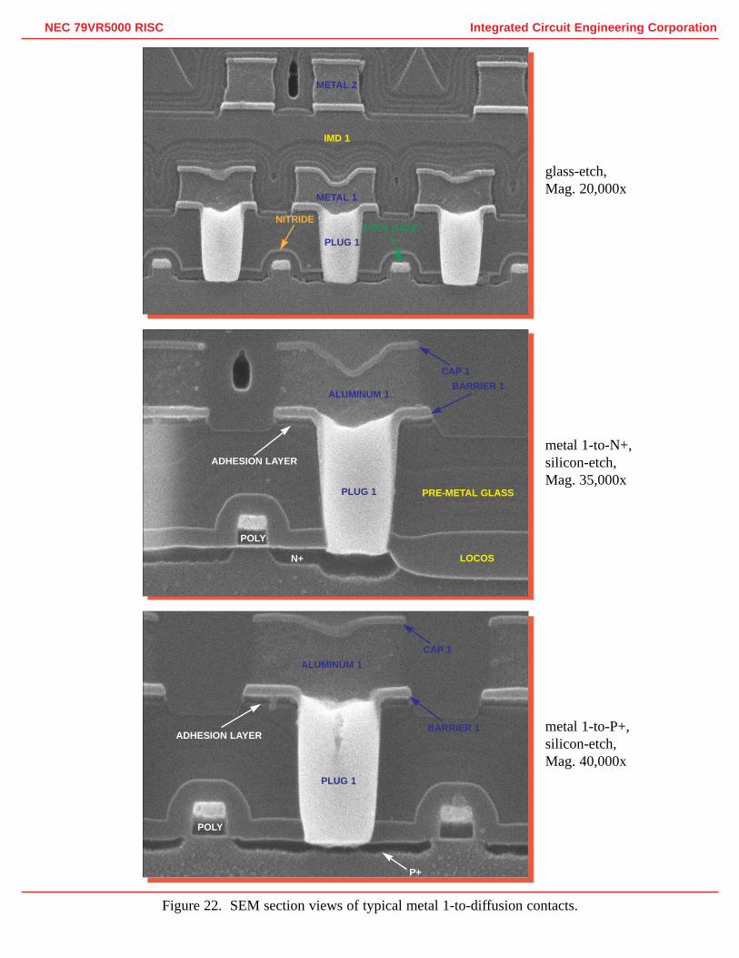
glass-etch,Mag. 20,000x
metal 1-to-N+,silicon-etch,Mag. 35,000x
metal 1-to-P+,silicon-etch,Mag. 40,000x
Integrated Circuit Engineering CorporationNEC 79VR5000 RISC
Figure 22. SEM section views of typical metal 1-to-diffusion contacts.
METAL 2
IMD 1
METAL 1
PLUG 1
NITRIDEPOLY GATE
PLUG 1
PLUG 1
POLY
ALUMINUM 1
CAP 1
BARRIER 1ADHESION LAYER
P+
BARRIER 1ALUMINUM 1
ADHESION LAYER
POLY
CAP 1
PRE-METAL GLASS
LOCOSN+
Integrated Circuit Engineering CorporationNEC 79VR5000 RISC
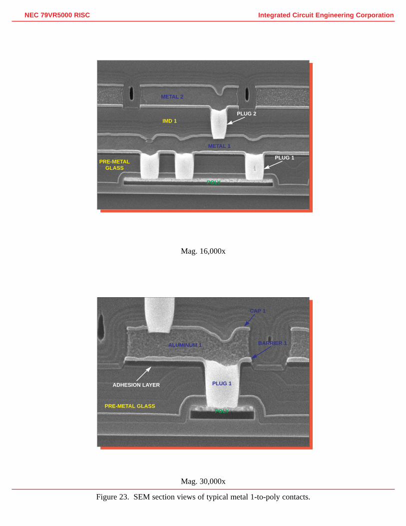
Mag. 30,000x
Mag. 16,000x
Figure 23. SEM section views of typical metal 1-to-poly contacts.
METAL 2
IMD 1PLUG 2
METAL 1
POLY
PLUG 1PRE-METAL
GLASS
CAP 1
BARRIER 1
PLUG 1
POLY
ADHESION LAYER
ALUMINUM 1
PRE-METAL GLASS
Mag. 5000x
Mag. 10,000x
Mag. 30,000x
Integrated Circuit Engineering CorporationNEC 79VR5000 RISC
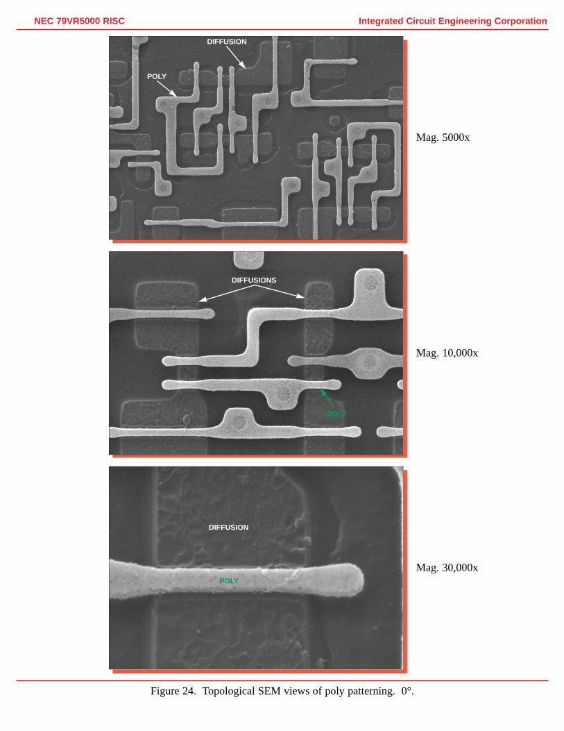
Figure 24. Topological SEM views of poly patterning. 0°.
DIFFUSION
POLY
DIFFUSIONS
POLY
POLY
DIFFUSION
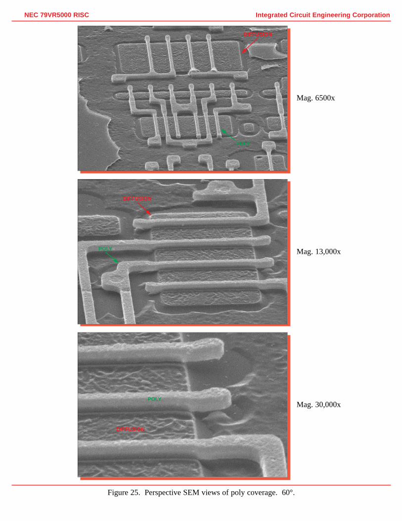
Mag. 6500x
Mag. 13,000x
Mag. 30,000x
Integrated Circuit Engineering CorporationNEC 79VR5000 RISC
Figure 25. Perspective SEM views of poly coverage. 60°.
DIFFUSION
DIFFUSION
POLY
POLY
POLY
DIFFUSION
Integrated Circuit Engineering CorporationNEC 79VR5000 RISC
Figure 26. SEM section views of typical transistors. Mag. 52,000x.
glass-etch
N-channel
P-channel
PRE-METALGLASS NITRIDE
POLY
POLY
P+ S/D
PLUG 1
PLUG 1
N+ S/D
GATE OXIDE
SILICIDE
NITRIDE
PLUG 1
POLY
SIDEWALLSPACER
SILICIDE
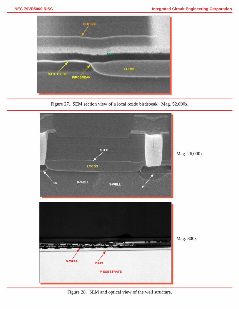
Figure 27. SEM section view of a local oxide birdsbeak. Mag. 52,000x.
Mag. 26,000x
Mag. 800x
Integrated Circuit Engineering CorporationNEC 79VR5000 RISC
Figure 28. SEM and optical view of the well structure.
NITRIDE
POLY
LOCOS
LOCOS
STEP
N+
N-WELLP-EPI
P-SUBSTRATE
P+N-WELL
P-WELL
GATE OXIDEBIRDSBEAK
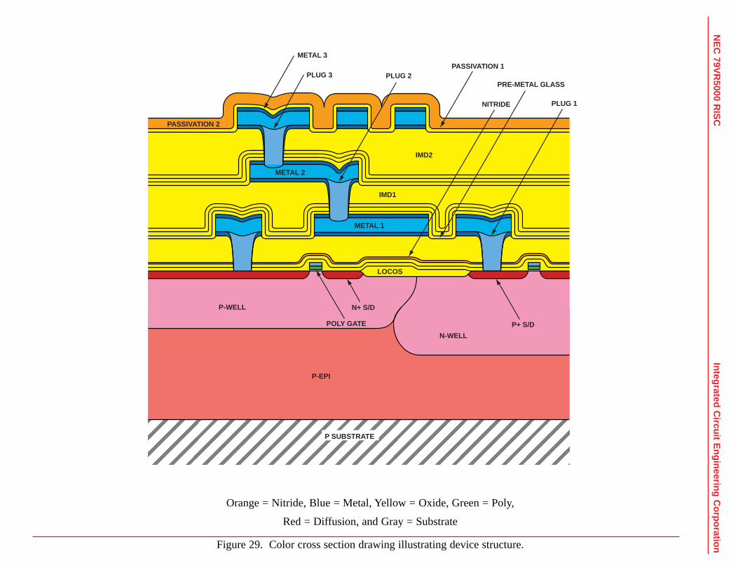
Figure 29. Color cross section drawing illustrating device structure.
Orange = Nitride, Blue = Metal, Yellow = Oxide, Green = Poly,
Red = Diffusion, and Gray = Substrate
Integrated Circuit E
ngineering Corporation
NE
C 79V
R5000 R
ISC
����������������������������
PASSIVATION 2
PASSIVATION 1
METAL 3
METAL 2
METAL 1
PLUG 3 PLUG 2
PLUG 1
IMD2
IMD1
PRE-METAL GLASS
P-WELL N+ S/D
P+ S/D
N-WELL
P-EPI
P SUBSTRATE
LOCOS
POLY GATE
NITRIDE
Integrated Circuit Engineering CorporationNEC 79VR5000 RISC
metal 2
metal 3
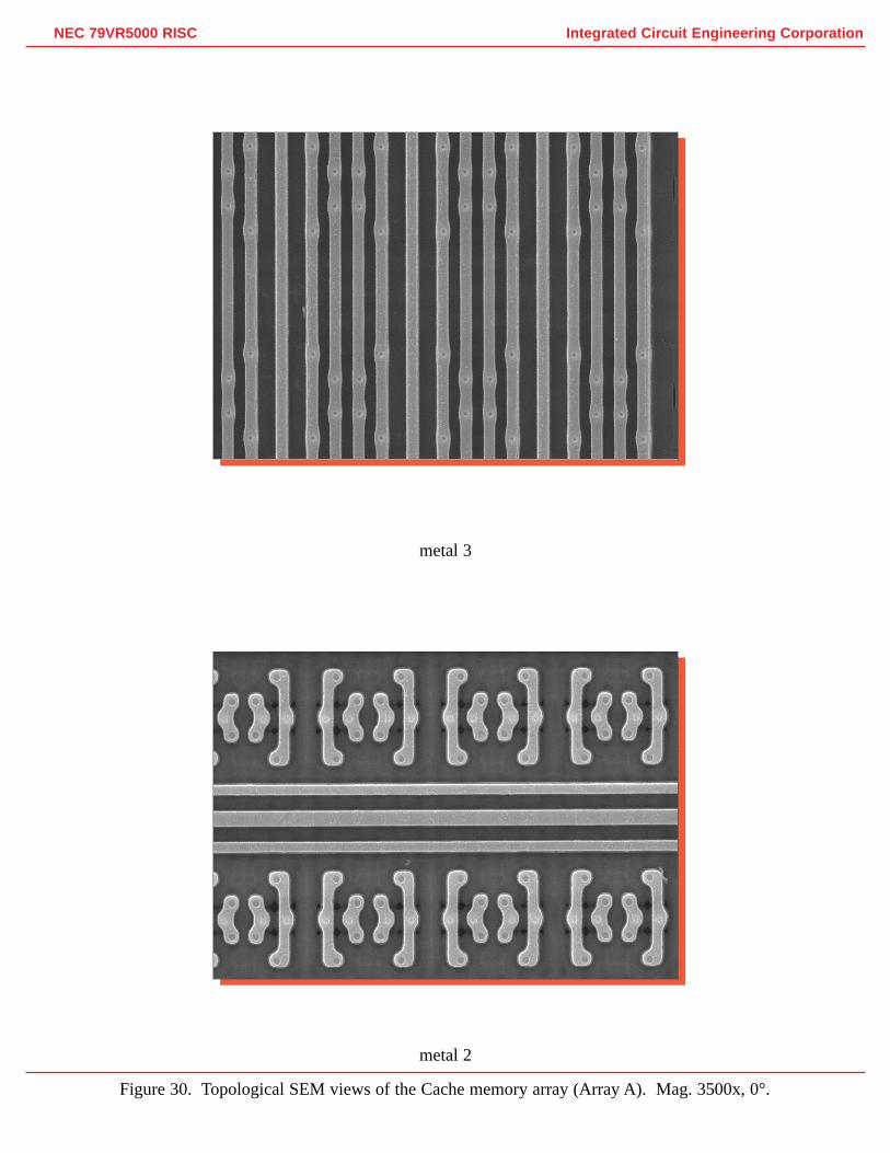
Figure 30. Topological SEM views of the Cache memory array (Array A). Mag. 3500x, 0°.
Integrated Circuit Engineering CorporationNEC 79VR5000 RISC
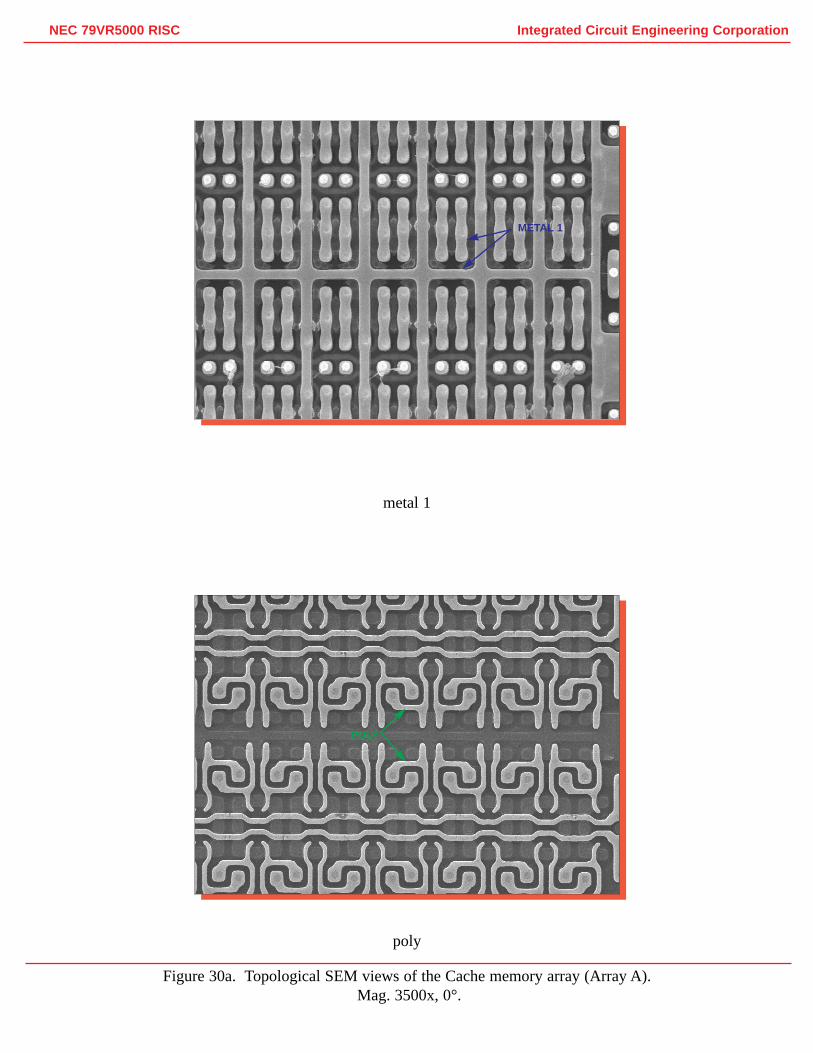
poly
metal 1
Figure 30a. Topological SEM views of the Cache memory array (Array A). Mag. 3500x, 0°.
METAL 1
POLY
Integrated Circuit Engineering CorporationNEC 79VR5000 RISC
metal 2
metal 3
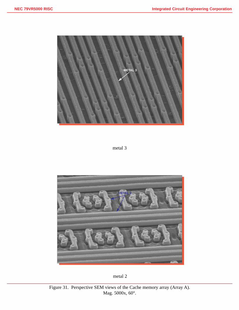
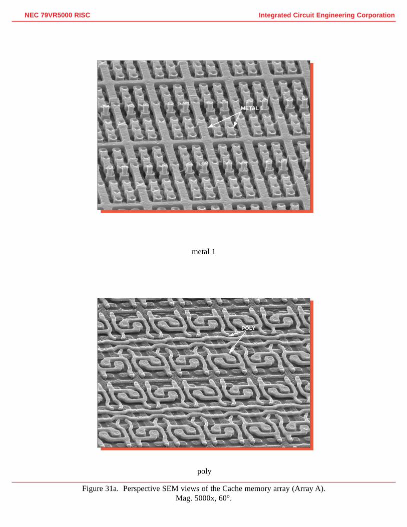
Figure 31. Perspective SEM views of the Cache memory array (Array A). Mag. 5000x, 60°.
METAL 3
METAL 2
Integrated Circuit Engineering CorporationNEC 79VR5000 RISC
poly
metal 1
Figure 31a. Perspective SEM views of the Cache memory array (Array A). Mag. 5000x, 60°.
METAL 1
POLY
Integrated Circuit Engineering CorporationNEC 79VR5000 RISC
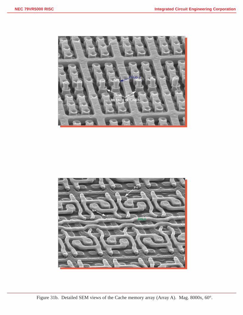
Figure 31b. Detailed SEM views of the Cache memory array (Array A). Mag. 8000x, 60°.
PLUG 2
METAL 1 BITLINES
POLY
P+
N+
Integrated Circuit Engineering CorporationNEC 79VR5000 RISC
metal 2
metal 3
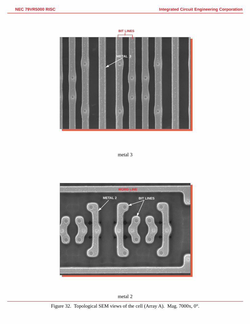
Figure 32. Topological SEM views of the cell (Array A). Mag. 7000x, 0°.
METAL 3
BIT LINES
METAL 2 BIT LINES
WORD LINE
metal 1
poly
Integrated Circuit Engineering CorporationNEC 79VR5000 RISC
WORD
BIT
1
2
3
4
56BIT
Figure 33. Topological SEM views of the cell along with the schematic (Array A). Mag. 7000x, 0°.
VCCWORD
GND
BIT LINES
POLY
P+
N+
1
2
3
4
56
WORDLINE
GND
VCC

Mag. 4000x
Mag. 8000x
Mag. 26,000x
Integrated Circuit Engineering CorporationNEC 79VR5000 RISC
Figure 34. SEM section views of the Cache memory array (Array A).
METAL 2
METAL 1
N-WELLS
N-WELL
METAL 1 BITCONTACT
POLY WORD LINE
N+
P+N+
P-WELL
METAL 1 BIT LINE
METAL 2
Integrated Circuit Engineering CorporationNEC 79VR5000 RISC
Mag. 26,000x
Mag. 8000x
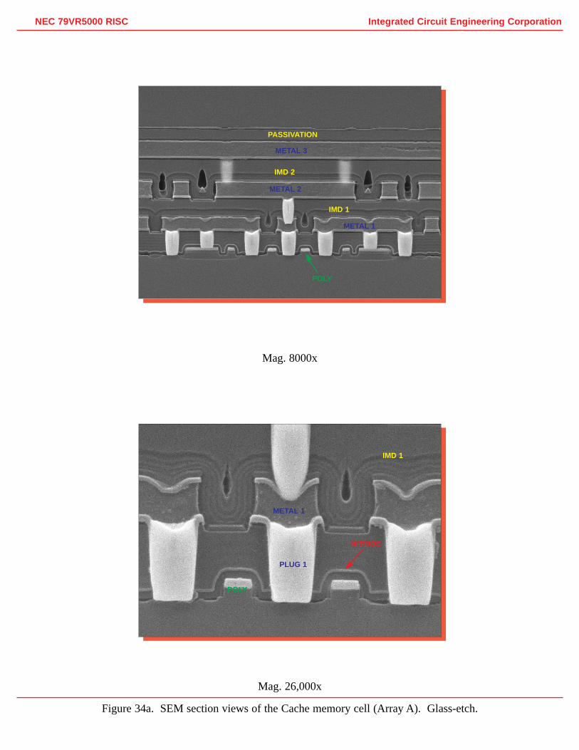
Figure 34a. SEM section views of the Cache memory cell (Array A). Glass-etch.
PASSIVATION
METAL 3
IMD 2
METAL 2
IMD 1
METAL 1
POLY
METAL 1
IMD 1
PLUG 1
NITRIDE
POLY
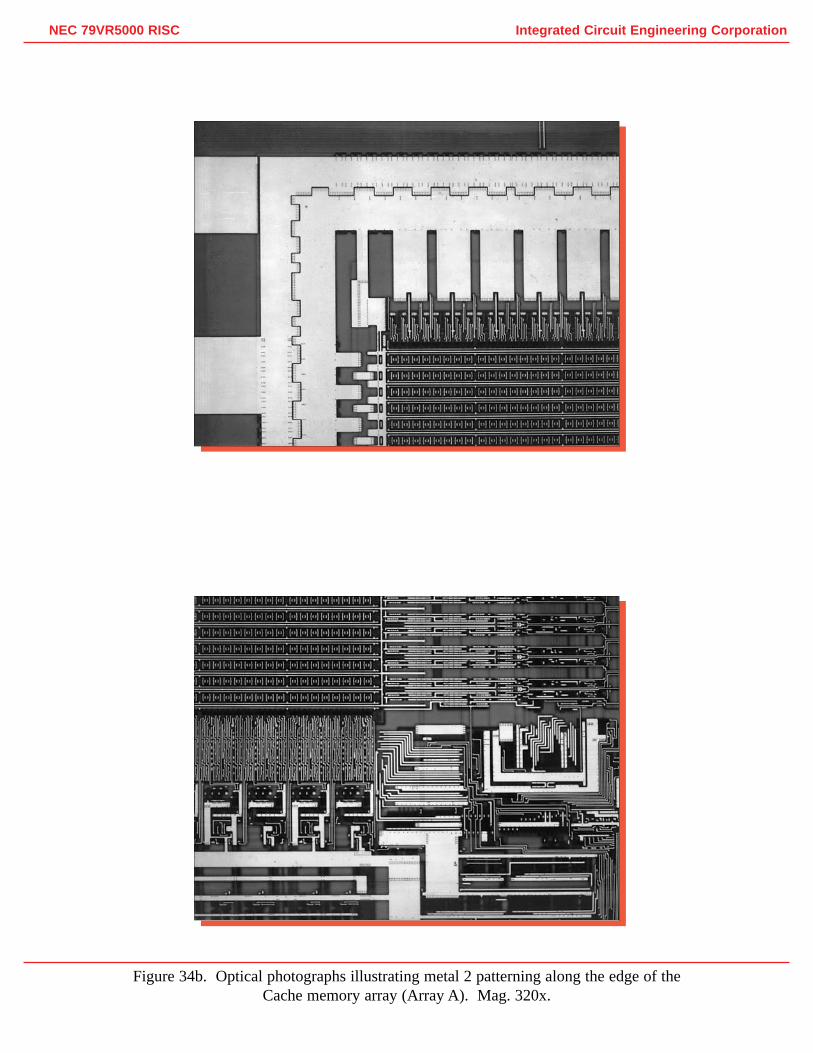
Figure 34b. Optical photographs illustrating metal 2 patterning along the edge of theCache memory array (Array A). Mag. 320x.
Integrated Circuit Engineering CorporationNEC 79VR5000 RISC
Integrated Circuit Engineering CorporationNEC 79VR5000 RISC
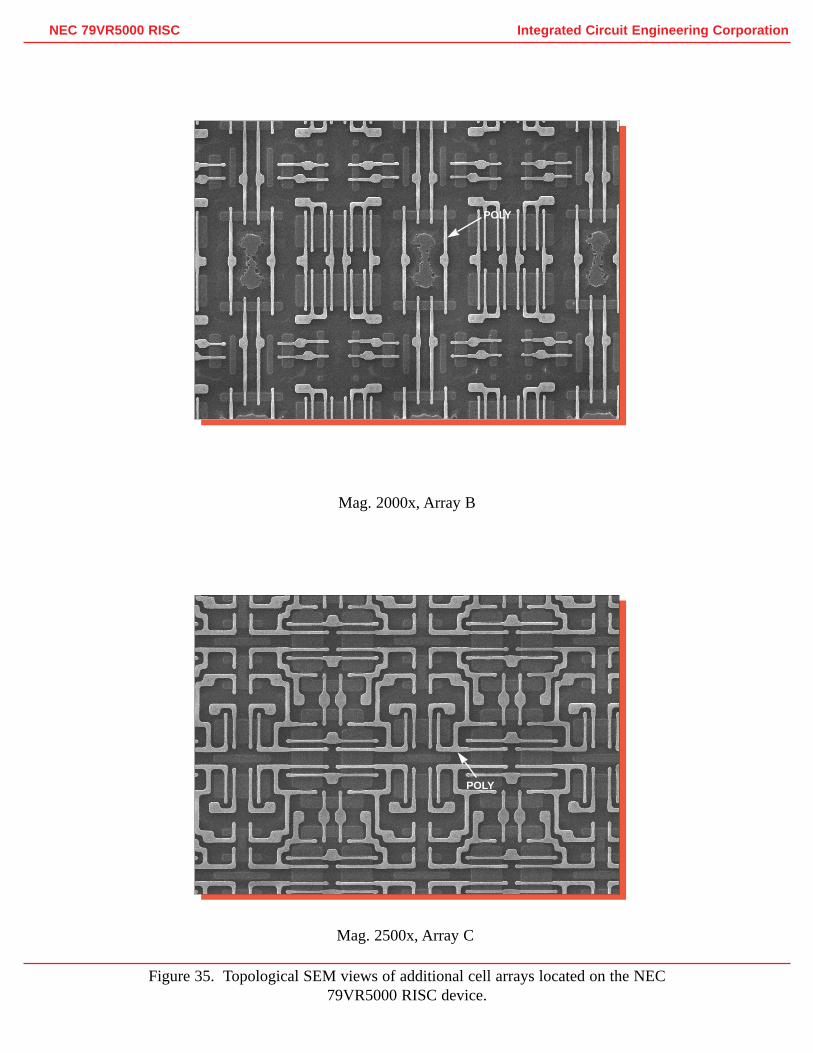
Mag. 2500x, Array C
Mag. 2000x, Array B
Figure 35. Topological SEM views of additional cell arrays located on the NEC79VR5000 RISC device.
POLY
POLY
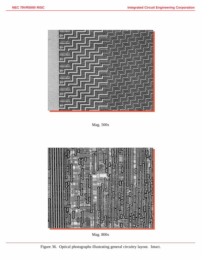
Mag. 800x
Mag. 500x
Figure 36. Optical photographs illustrating general circuitry layout. Intact.
Integrated Circuit Engineering CorporationNEC 79VR5000 RISC
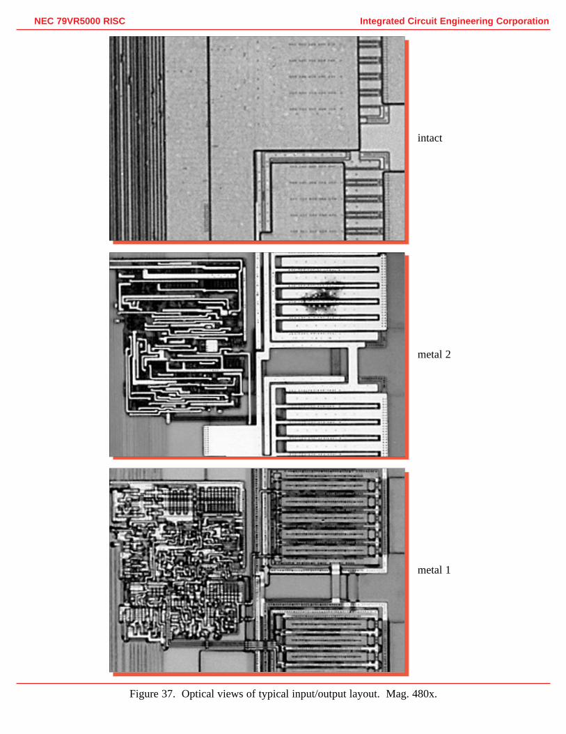
intact
metal 2
metal 1
Integrated Circuit Engineering CorporationNEC 79VR5000 RISC
Figure 37. Optical views of typical input/output layout. Mag. 480x.