NCN49597 - Power Line Communication Modem
30
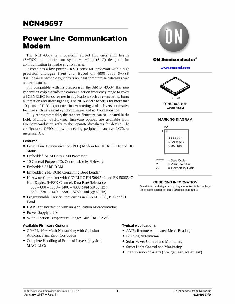
© Semiconductor Components Industries, LLC, 2017 January, 2017 - Rev. 4 1 Publication Order Number: NCN49597/D NCN49597 Power Line Communication Modem The NCN49597 is a powerful spread frequency shift keying (S-FSK) communication system-on-chip (SoC) designed for communication in hostile environments. It combines a low power ARM Cortex M0 processor with a high precision analogue front end. Based on 4800 baud S-FSK dual-channel technology, it offers an ideal compromise between speed and robustness. Pin-compatible with its predecessor, the AMIS-49587, this new generation chip extends the communication frequency range to cover all CENELEC bands for use in applications such as e-metering, home automation and street lighting. The NCN49597 benefits for more than 10 years of field experience in e-metering and delivers innovative features such as a smart synchronization and in-band statistics. Fully reprogrammable, the modem firmware can be updated in the field. Multiple royalty-free firmware options are available from ON Semiconductor; refer to the separate datasheets for details. The configurable GPIOs allow connecting peripherals such as LCDs or metering ICs. Features • Power Line Communication (PLC) Modem for 50 Hz, 60 Hz and DC Mains • Embedded ARM Cortex M0 Processor • 10 General Purpose IOs Controllable by Software • Embedded 32 kB RAM • Embedded 2 kB ROM Containing Boot Loader • Hardware Compliant with CENELEC EN 50065-1 and EN 50065-7 Half Duplex S-FSK Channel, Data Rate Selectable: 300 – 600 – 1200 – 2400 – 4800 baud (@ 50 Hz); 360 – 720 – 1440 – 2880 – 5760 baud (@ 60 Hz) • Programmable Carrier Frequencies in CENELEC A, B, C and D Band • UART for Interfacing with an Application Microcontroller • Power Supply 3.3 V • Wide Junction Temperature Range: -40°C to +125°C Available Firmware Options • ON-PL110 - Mesh Networking with Collision Avoidance and Error Correction • Complete Handling of Protocol Layers (physical, MAC, LLC) Typical Applications • AMR: Remote Automated Meter Reading • Building Automation • Solar Power Control and Monitoring • Street Light Control and Monitoring • Transmission of Alerts (fire, gas leak, water leak) See detailed ordering and shipping information in the package dimensions section on page 29 of this data sheet. ORDERING INFORMATION XXXX = Date Code Y = Plant Identifier ZZ = Traceability Code www. onsemi.com MARKING DIAGRAM 1 52 QFN52 8x8, 0.5P CASE 485M XXXXYZZ NCN 49597 C597-901 1 52
Transcript of NCN49597 - Power Line Communication Modem
© Semiconductor Components Industries, LLC, 2017
January, 2017 − Rev. 41 Publication Order Number:
NCN49597/D
NCN49597
Power Line Communication
Modem
The NCN49597 is a powerful spread frequency shift keying(S−FSK) communication system−on−chip (SoC) designed forcommunication in hostile environments.
It combines a low power ARM Cortex M0 processor with a highprecision analogue front end. Based on 4800 baud S−FSKdual−channel technology, it offers an ideal compromise between speedand robustness.
Pin−compatible with its predecessor, the AMIS−49587, this newgeneration chip extends the communication frequency range to coverall CENELEC bands for use in applications such as e−metering, homeautomation and street lighting. The NCN49597 benefits for more than10 years of field experience in e−metering and delivers innovativefeatures such as a smart synchronization and in−band statistics.
Fully reprogrammable, the modem firmware can be updated in thefield. Multiple royalty−free firmware options are available fromON Semiconductor; refer to the separate datasheets for details. Theconfigurable GPIOs allow connecting peripherals such as LCDs ormetering ICs.
Features• Power Line Communication (PLC) Modem for 50 Hz, 60 Hz and DC
Mains• Embedded ARM Cortex M0 Processor
• 10 General Purpose IOs Controllable by Software
• Embedded 32 kB RAM
• Embedded 2 kB ROM Containing Boot Loader
• Hardware Compliant with CENELEC EN 50065−1 and EN 50065−7Half Duplex S−FSK Channel, Data Rate Selectable:
300 – 600 – 1200 – 2400 – 4800 baud (@ 50 Hz);360 – 720 – 1440 – 2880 – 5760 baud (@ 60 Hz)
• Programmable Carrier Frequencies in CENELEC A, B, C and DBand
• UART for Interfacing with an Application Microcontroller
• Power Supply 3.3 V
• Wide Junction Temperature Range: −40°C to +125°C
Available Firmware Options• ON−PL110 − Mesh Networking with Collision
Avoidance and Error Correction• Complete Handling of Protocol Layers (physical,
MAC, LLC)
Typical Applications• AMR: Remote Automated Meter Reading
• Building Automation
• Solar Power Control and Monitoring
• Street Light Control and Monitoring
• Transmission of Alerts (fire, gas leak, water leak)
See detailed ordering and shipping information in the packagedimensions section on page 29 of this data sheet.
ORDERING INFORMATION
XXXX = Date CodeY = Plant IdentifierZZ = Traceability Code
www.onsemi.com
MARKING DIAGRAM
1 52
QFN52 8x8, 0.5PCASE 485M
XXXXYZZNCN 49597C597−901
152
NCN49597
www.onsemi.com2
APPLICATION
Application Example
Figure 1. Typical Application for the NCN49597 S−FSK Modem
TX_OUT
NCN49597TX_ENB
ZC_IN
REF_OUT
RX_IN
RX_OUT
XT
AL_
IN
XT
AL_
OU
T
TXD
RXD
BR 0
BR 1
RESB
VS
SA
VS
SV
DD
VD
DA
3V3_A 3V3_D
1:2 C1
R1
C2
R2
C DREF
C16 C17
3V3_A
D5
D1
D2
D3
D4
R12
C11
C12
R14
C15
C14
Y1
NCS5651
Ena
ble
C3
C4
C6
C7
R6
R5 R4
R7
R9
R10
2Vcom+B
−B
+A
−A
OutA
OutB 89
13
12 54
3
1
6 7
VCC
10 11
VEE
Vuc19
151420
GNDuCRlim
Vwarn
3V3_D12 V
R11
C5
C10
C912 V
R3
MAINS
Tr
C8
C13
U1
U2
3V3_D
VDD1V8
R8
SEN
EXT_CLK_E
Application
MicroController
&Metering
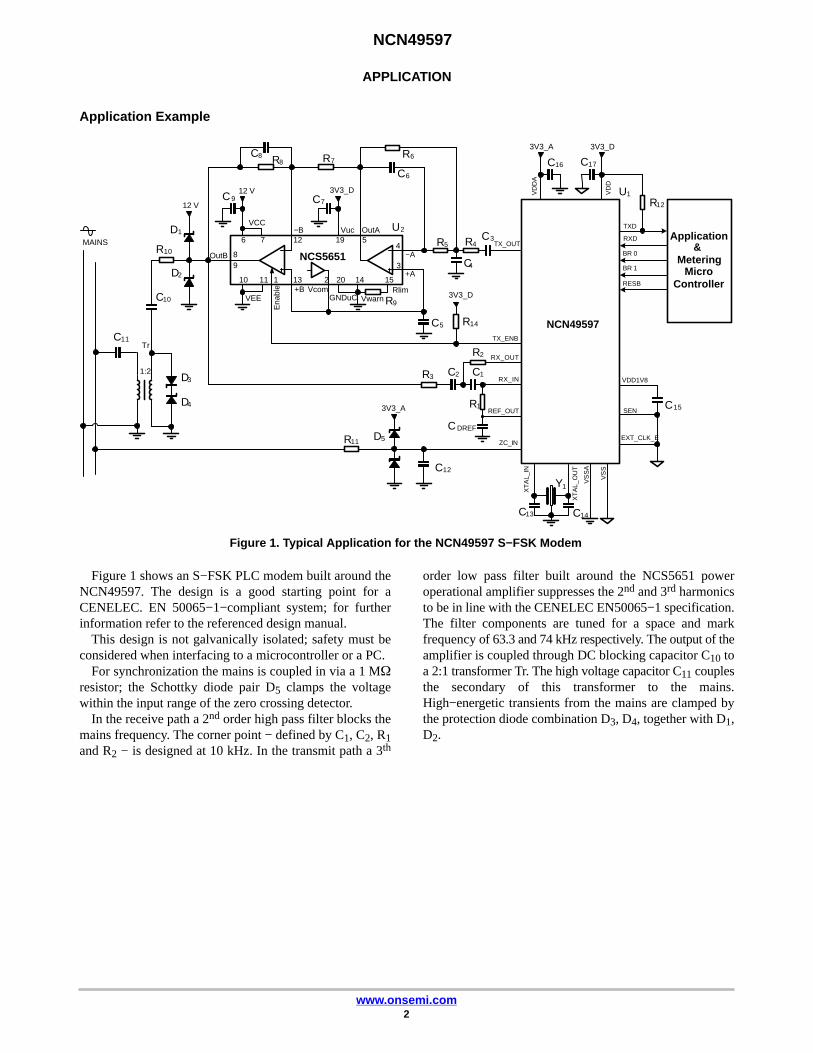
Figure 1 shows an S−FSK PLC modem built around theNCN49597. The design is a good starting point for aCENELEC. EN 50065−1−compliant system; for furtherinformation refer to the referenced design manual.
This design is not galvanically isolated; safety must beconsidered when interfacing to a microcontroller or a PC.
For synchronization the mains is coupled in via a 1 M�
resistor; the Schottky diode pair D5 clamps the voltagewithin the input range of the zero crossing detector.
In the receive path a 2nd order high pass filter blocks themains frequency. The corner point − defined by C1, C2, R1and R2 − is designed at 10 kHz. In the transmit path a 3th
order low pass filter built around the NCS5651 poweroperational amplifier suppresses the 2nd and 3rd harmonicsto be in line with the CENELEC EN50065−1 specification.The filter components are tuned for a space and markfrequency of 63.3 and 74 kHz respectively. The output of theamplifier is coupled through DC blocking capacitor C10 toa 2:1 transformer Tr. The high voltage capacitor C11 couplesthe secondary of this transformer to the mains.High−energetic transients from the mains are clamped bythe protection diode combination D3, D4, together with D1,D2.
NCN49597
www.onsemi.com3
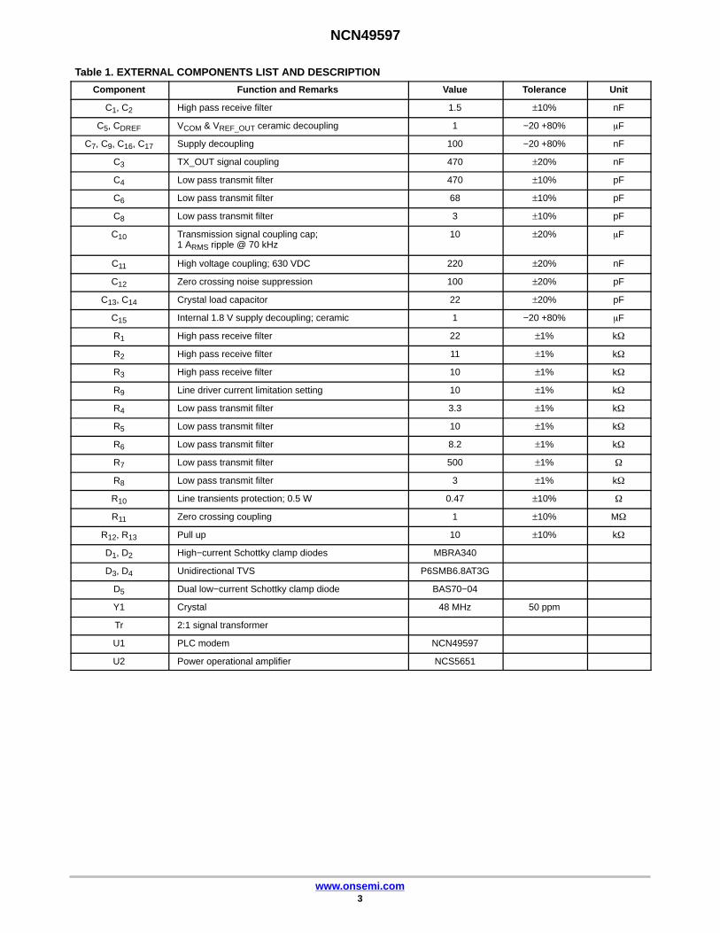
Table 1. EXTERNAL COMPONENTS LIST AND DESCRIPTION
Component Function and Remarks Value Tolerance Unit
C1, C2 High pass receive filter 1.5 ±10% nF
C5, CDREF VCOM & VREF_OUT ceramic decoupling 1 −20 +80% �F
C7, C9, C16, C17 Supply decoupling 100 −20 +80% nF
C3 TX_OUT signal coupling 470 ±20% nF
C4 Low pass transmit filter 470 ±10% pF
C6 Low pass transmit filter 68 ±10% pF
C8 Low pass transmit filter 3 ±10% pF
C10 Transmission signal coupling cap;1 ARMS ripple @ 70 kHz
10 ±20% �F
C11 High voltage coupling; 630 VDC 220 ±20% nF
C12 Zero crossing noise suppression 100 ±20% pF
C13, C14 Crystal load capacitor 22 ±20% pF
C15 Internal 1.8 V supply decoupling; ceramic 1 −20 +80% �F
R1 High pass receive filter 22 ±1% k�
R2 High pass receive filter 11 ±1% k�
R3 High pass receive filter 10 ±1% k�
R9 Line driver current limitation setting 10 ±1% k�
R4 Low pass transmit filter 3.3 ±1% k�
R5 Low pass transmit filter 10 ±1% k�
R6 Low pass transmit filter 8.2 ±1% k�
R7 Low pass transmit filter 500 ±1% �
R8 Low pass transmit filter 3 ±1% k�
R10 Line transients protection; 0.5 W 0.47 ±10% �
R11 Zero crossing coupling 1 ±10% M�
R12, R13 Pull up 10 ±10% k�
D1, D2 High−current Schottky clamp diodes MBRA340
D3, D4 Unidirectional TVS P6SMB6.8AT3G
D5 Dual low−current Schottky clamp diode BAS70−04
Y1 Crystal 48 MHz 50 ppm
Tr 2:1 signal transformer
U1 PLC modem NCN49597
U2 Power operational amplifier NCS5651
NCN49597
www.onsemi.com4
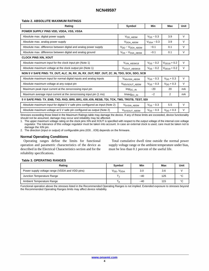
Table 2. ABSOLUTE MAXIMUM RATINGS
Rating Symbol Min Max Unit
POWER SUPPLY PINS VDD, VDDA, VSS, VSSA
Absolute max. digital power supply VDD_ABSM VSS − 0.3 3.9 V
Absolute max. analog power supply VDDA_ABSM VSSA − 0.3 3.9 V
Absolute max. difference between digital and analog power supply VDD − VDDA_ABSM −0.1 0.1 V
Absolute max. difference between digital and analog ground VSS − VSSA_ABSM −0.1 0.1 V
CLOCK PINS XIN, XOUT
Absolute maximum input for the clock input pin (Note 1) VXIN_ABSM18 VSS − 0.2 VDD18 + 0.2 V
Absolute maximum voltage at the clock output pin (Note 1) VXOUT_ABSM18 VSS − 0.2 VDD18 + 0.2 V
NON 5 V SAFE PINS: TX_OUT, ALC_IN, RX_IN, RX_OUT, REF_OUT, ZC_IN, TDO, SCK, SDO, SCB
Absolute maximum input for normal digital inputs and analog inputs VN5VSIN_ABSM VSS − 0.3 VDD + 0.3 V
Absolute maximum voltage at any output pin VN5VSOUT_ABSM VSS − 0.3 VDD + 0.3 V
Maximum peak input current at the zerocrossing input pin ImpZC_IN −20 20 mA
Maximum average input current at the zerocrossing input pin (1 ms) ImavgZC_IN −2 2 mA
5 V SAFE PINS: TX_ENB, TXD, RXD, BR0, BR1, IO0..IO9, RESB, TDI, TCK, TMS, TRSTB, TEST, SDI
Absolute maximum input for digital 5 V safe pins configured as input (Note 2) V5VSIN_ABSM VSS − 0.3 5.5 V
Absolute maximum voltage at 5 V safe pin configured as output (Note 2) V5VSOUT_ABSM VSS − 0.3 VDD + 0.3 V
Stresses exceeding those listed in the Maximum Ratings table may damage the device. If any of these limits are exceeded, device functionalityshould not be assumed, damage may occur and reliability may be affected.1. The upper maximum voltage rating on the clock pins XIN and XOUT is specified with respect to the output voltage of the internal core voltage
regulator. The tolerance of this voltage regulator must be taken into account. In case an external clock is used, care must be taken not todamage the XIN pin.
2. The direction (input or output) of configurable pins (IO0…IO9) depends on the firmware.
Normal Operating ConditionsOperating ranges define the limits for functional
operation and parametric characteristics of the device asdescribed in the Electrical Characteristics section and for thereliability specifications.
Total cumulative dwell time outside the normal powersupply voltage range or the ambient temperature under bias,must be less than 0.1 percent of the useful life.
Table 3. OPERATING RANGES
Rating Symbol Min Max Unit
Power supply voltage range (VDDA and VDD pins) VDD, VDDA 3.0 3.6 V
Junction Temperature Range TJ −40 125 °C
Ambient Temperature Range TA −40 115 °C
Functional operation above the stresses listed in the Recommended Operating Ranges is not implied. Extended exposure to stresses beyondthe Recommended Operating Ranges limits may affect device reliability.
NCN49597
www.onsemi.com5
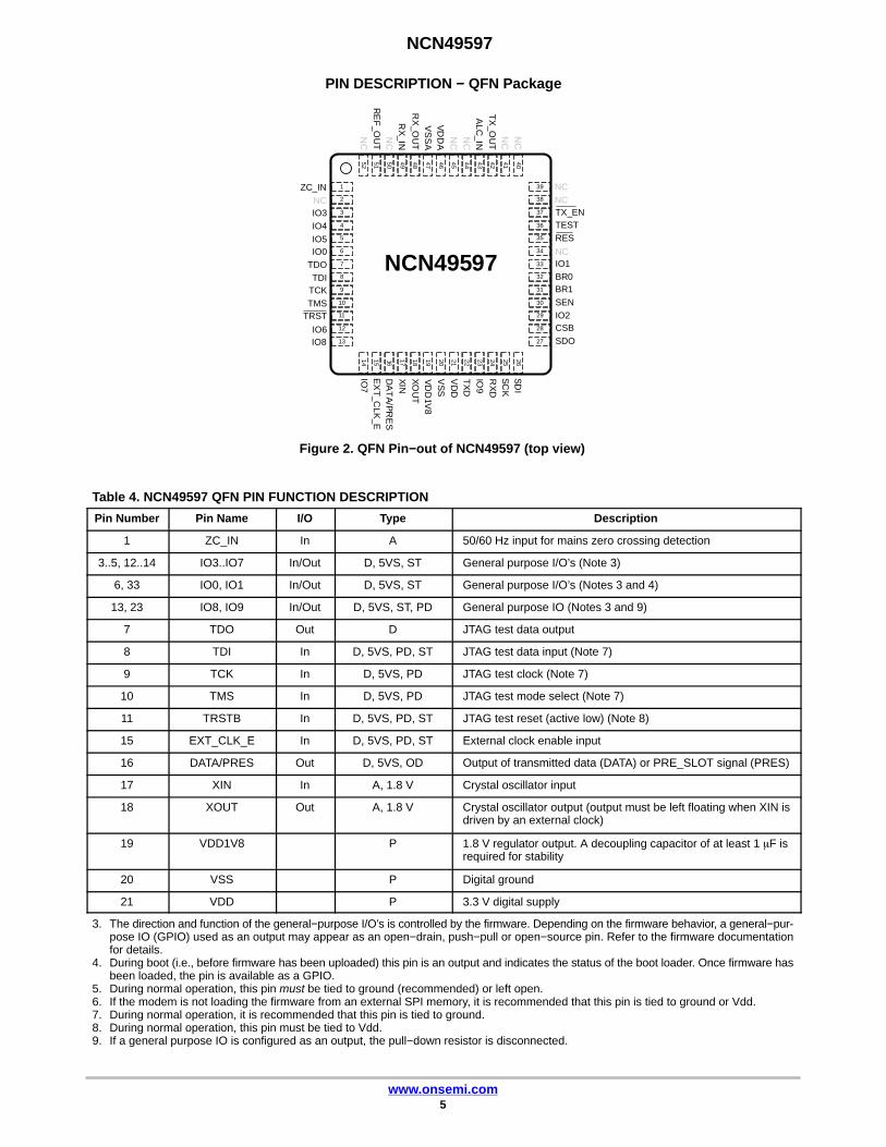
PIN DESCRIPTION − QFN Package
NCN49597
1
2
3
4
5
6
7
8
9
10
11
12
13
26252423222120191817161514
39
38
37
36
35
34
33
32
31
30
29
28
27
40414243444546474849505152N
CR
EF
_OU
TN
CR
X_IN
RX
_OU
TV
SS
AV
DD
AN
CN
CA
LC_IN
TX
_OU
TN
CN
C
IO8
DA
TA
/PR
ES
XIN
XO
UT
VD
D1V
8V
SS
VD
DT
XD
IO9
RX
DS
CK
SD
I
IO7
IO6
TMSTCKTDI
TDOIO0IO5IO4IO3NC
ZC_IN
SDOCSBIO2SENBR1BR0IO1
TEST
NCNC
TRST
RES
TX_EN
EX
T_C
LK_E
NC
Figure 2. QFN Pin−out of NCN49597 (top view)
Table 4. NCN49597 QFN PIN FUNCTION DESCRIPTION
Pin Number Pin Name I/O Type Description
1 ZC_IN In A 50/60 Hz input for mains zero crossing detection
3..5, 12..14 IO3..IO7 In/Out D, 5VS, ST General purpose I/O’s (Note 3)
6, 33 IO0, IO1 In/Out D, 5VS, ST General purpose I/O’s (Notes 3 and 4)
13, 23 IO8, IO9 In/Out D, 5VS, ST, PD General purpose IO (Notes 3 and 9)
7 TDO Out D JTAG test data output
8 TDI In D, 5VS, PD, ST JTAG test data input (Note 7)
9 TCK In D, 5VS, PD JTAG test clock (Note 7)
10 TMS In D, 5VS, PD JTAG test mode select (Note 7)
11 TRSTB In D, 5VS, PD, ST JTAG test reset (active low) (Note 8)
15 EXT_CLK_E In D, 5VS, PD, ST External clock enable input
16 DATA/PRES Out D, 5VS, OD Output of transmitted data (DATA) or PRE_SLOT signal (PRES)
17 XIN In A, 1.8 V Crystal oscillator input
18 XOUT Out A, 1.8 V Crystal oscillator output (output must be left floating when XIN isdriven by an external clock)
19 VDD1V8 P 1.8 V regulator output. A decoupling capacitor of at least 1 �F isrequired for stability
20 VSS P Digital ground
21 VDD P 3.3 V digital supply
3. The direction and function of the general−purpose I/O’s is controlled by the firmware. Depending on the firmware behavior, a general−pur-pose IO (GPIO) used as an output may appear as an open−drain, push−pull or open−source pin. Refer to the firmware documentationfor details.
4. During boot (i.e., before firmware has been uploaded) this pin is an output and indicates the status of the boot loader. Once firmware hasbeen loaded, the pin is available as a GPIO.
5. During normal operation, this pin must be tied to ground (recommended) or left open.6. If the modem is not loading the firmware from an external SPI memory, it is recommended that this pin is tied to ground or Vdd.7. During normal operation, it is recommended that this pin is tied to ground.8. During normal operation, this pin must be tied to Vdd.9. If a general purpose IO is configured as an output, the pull−down resistor is disconnected.
NCN49597
www.onsemi.com6
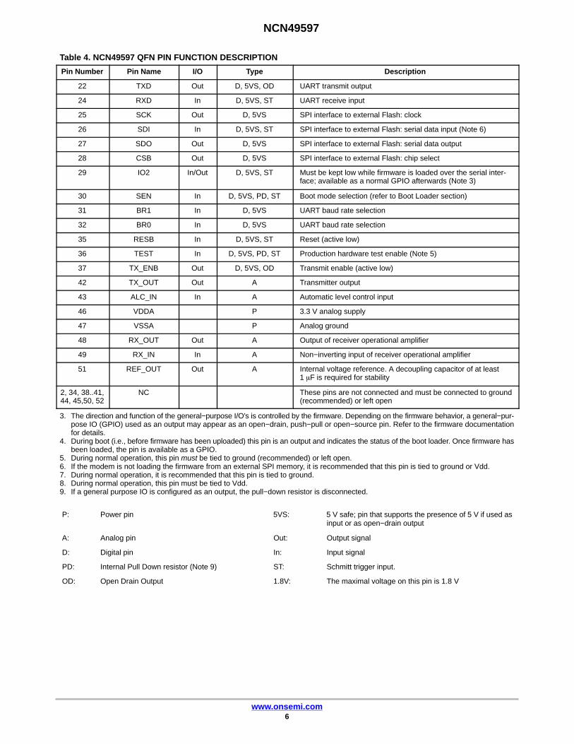
Table 4. NCN49597 QFN PIN FUNCTION DESCRIPTION
Pin Number DescriptionTypeI/OPin Name
22 TXD Out D, 5VS, OD UART transmit output
24 RXD In D, 5VS, ST UART receive input
25 SCK Out D, 5VS SPI interface to external Flash: clock
26 SDI In D, 5VS, ST SPI interface to external Flash: serial data input (Note 6)
27 SDO Out D, 5VS SPI interface to external Flash: serial data output
28 CSB Out D, 5VS SPI interface to external Flash: chip select
29 IO2 In/Out D, 5VS, ST Must be kept low while firmware is loaded over the serial inter-face; available as a normal GPIO afterwards (Note 3)
30 SEN In D, 5VS, PD, ST Boot mode selection (refer to Boot Loader section)
31 BR1 In D, 5VS UART baud rate selection
32 BR0 In D, 5VS UART baud rate selection
35 RESB In D, 5VS, ST Reset (active low)
36 TEST In D, 5VS, PD, ST Production hardware test enable (Note 5)
37 TX_ENB Out D, 5VS, OD Transmit enable (active low)
42 TX_OUT Out A Transmitter output
43 ALC_IN In A Automatic level control input
46 VDDA P 3.3 V analog supply
47 VSSA P Analog ground
48 RX_OUT Out A Output of receiver operational amplifier
49 RX_IN In A Non−inverting input of receiver operational amplifier
51 REF_OUT Out A Internal voltage reference. A decoupling capacitor of at least1 �F is required for stability
2, 34, 38..41,44, 45,50, 52
NC These pins are not connected and must be connected to ground(recommended) or left open
3. The direction and function of the general−purpose I/O’s is controlled by the firmware. Depending on the firmware behavior, a general−pur-pose IO (GPIO) used as an output may appear as an open−drain, push−pull or open−source pin. Refer to the firmware documentationfor details.
4. During boot (i.e., before firmware has been uploaded) this pin is an output and indicates the status of the boot loader. Once firmware hasbeen loaded, the pin is available as a GPIO.
5. During normal operation, this pin must be tied to ground (recommended) or left open.6. If the modem is not loading the firmware from an external SPI memory, it is recommended that this pin is tied to ground or Vdd.7. During normal operation, it is recommended that this pin is tied to ground.8. During normal operation, this pin must be tied to Vdd.9. If a general purpose IO is configured as an output, the pull−down resistor is disconnected.
P: Power pin 5VS: 5 V safe; pin that supports the presence of 5 V if used asinput or as open−drain output
A: Analog pin Out: Output signal
D: Digital pin In: Input signal
PD: Internal Pull Down resistor (Note 9) ST: Schmitt trigger input.
OD: Open Drain Output 1.8V: The maximal voltage on this pin is 1.8 V
NCN49597
www.onsemi.com7
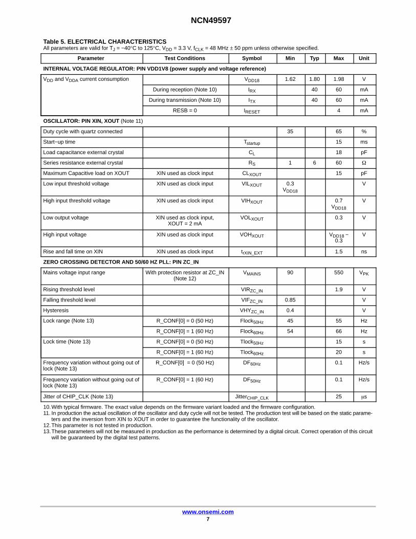
Table 5. ELECTRICAL CHARACTERISTICSAll parameters are valid for TJ = −40°C to 125°C, VDD = 3.3 V, fCLK = 48 MHz ± 50 ppm unless otherwise specified.
Parameter Test Conditions Symbol Min Typ Max Unit
INTERNAL VOLTAGE REGULATOR: PIN VDD1V8 (power supply and voltage reference)
VDD and VDDA current consumption VDD18 1.62 1.80 1.98 V
During reception (Note 10) IRX 40 60 mA
During transmission (Note 10) ITX 40 60 mA
RESB = 0 IRESET 4 mA
OSCILLATOR: PIN XIN, XOUT (Note 11)
Duty cycle with quartz connected 35 65 %
Start−up time Tstartup 15 ms
Load capacitance external crystal CL 18 pF
Series resistance external crystal RS 1 6 60 �
Maximum Capacitive load on XOUT XIN used as clock input CLXOUT 15 pF
Low input threshold voltage XIN used as clock input VILXOUT 0.3VDD18
V
High input threshold voltage XIN used as clock input VIHXOUT 0.7VDD18
V
Low output voltage XIN used as clock input,XOUT = 2 mA
VOLXOUT 0.3 V
High input voltage XIN used as clock input VOHXOUT VDD18 −0.3
V
Rise and fall time on XIN XIN used as clock input trXIN_EXT 1.5 ns
ZERO CROSSING DETECTOR AND 50/60 HZ PLL: PIN ZC_IN
Mains voltage input range With protection resistor at ZC_IN(Note 12)
VMAINS 90 550 VPK
Rising threshold level VIRZC_IN 1.9 V
Falling threshold level VIFZC_IN 0.85 V
Hysteresis VHYZC_IN 0.4 V
Lock range (Note 13) R_CONF[0] = 0 (50 Hz) Flock50Hz 45 55 Hz
R_CONF[0] = 1 (60 Hz) Flock60Hz 54 66 Hz
Lock time (Note 13) R_CONF[0] = 0 (50 Hz) Tlock50Hz 15 s
R_CONF[0] = 1 (60 Hz) Tlock60Hz 20 s
Frequency variation without going out oflock (Note 13)
R_CONF[0] = 0 (50 Hz) DF60Hz 0.1 Hz/s
Frequency variation without going out oflock (Note 13)
R_CONF[0] = 1 (60 Hz) DF50Hz 0.1 Hz/s
Jitter of CHIP_CLK (Note 13) JitterCHIP_CLK 25 �s
10.With typical firmware. The exact value depends on the firmware variant loaded and the firmware configuration.11. In production the actual oscillation of the oscillator and duty cycle will not be tested. The production test will be based on the static parame-
ters and the inversion from XIN to XOUT in order to guarantee the functionality of the oscillator.12.This parameter is not tested in production.13.These parameters will not be measured in production as the performance is determined by a digital circuit. Correct operation of this circuit
will be guaranteed by the digital test patterns.

NCN49597
www.onsemi.com8
Table 5. ELECTRICAL CHARACTERISTICSAll parameters are valid for TJ = −40°C to 125°C, VDD = 3.3 V, fCLK = 48 MHz ± 50 ppm unless otherwise specified.
Parameter UnitMaxTypMinSymbolTest Conditions
TRANSMITTER EXTERNAL PARAMETERS: PIN TX_OUT, ALC_IN, TX_ENB
AC output level fTX_OUT = 23 – 75 kHz (Note 14)fTX_OUT = 148.5 kHz (Note 14)
VTX_OUT 0.850.76
1.151.22
VPK
DC output level VTX_OUT 1.65 V
Second order harmonic distortion fTX_OUT = 148.5 kHz (Note 14) HD2 −55 dB
Third order harmonic distortion fTX_OUT = 148.5 kHz (Note 14) HD3 −57 dB
Transmitted carrier frequency resolution RfTX_OUT 11.44 11.44 Hz
Transmitted carrier frequency accuracy (Note 15) DfTX_OUT 30 Hz
Capacitive output load at pin TX_OUT (Note 15) CLTX_OUT 20 pF
Resistive output load at pin TX_OUT RLTX_OUT 5 5 k�
Turn off delay of TX_ENB output TdTX_ENB 0.25 0.5 ms
Automatic level control attenuation step ALCstep 2.9 3.1 dB
Maximum attenuation ALCrange 20.3 21.7 dB
Low threshold level on ALC_IN With DC bias equal to VREF_OUT VTLALC_IN 0.34 0.46 VPK
High threshold level on ALC_IN With DC bias equal to VREF_OUT VTHALC_IN 0.54 0.72 VPK
Input impedance of ALC_IN pin RALC_IN 111 189 k�
Power supply rejection ratio of thetransmitter section
f = 50 Hz (Note 16)f = 10 kHz (Note 16)
PSRRTX_OUT 3210
dB
Transmit cascade gain (Note 17) f = 10 kHzf = 148.5 kHzf = 195 kHzf = 245 kHzf = 500 kHzf = 1 MHzf = 2 MHz
VTX_PF_10kHzVTX_LPF_148kHz5VTX_LPF_195kHzVTX_LPF_245kHzVTX_LPF_500kHzVTX_LPF_1000kHzVTX_LPF_2000kHz
−0.5−1.3−4.5
−36−50
0.50.5−1.5−3−18
dB
14.With the level control register set for maximal output amplitude. Tested with low pass filter tuned for CENELEC D−band.15.This parameter will not be tested in production.16.A sinusoidal signal of 100 mVpp is injected between VDDA and VSSA while the digital AD converter generates an idle pattern. The signal
level at TX_OUT is measured to determine the parameter.17.The cascade of the digital−to−analog converter (DAC), low−pass filter (LPF), and transmission amplifier is production tested and must
have a frequency characteristic between the limits listed. The level is specified relative to the level at DC; the absolute output level willdepend on the operating condition.This test is done with the low−pass filter (LPF) tuned to include the CENELEC D−band. In production the measurement will be done forrelative to DC with a signal amplitude of 100 mV.
NCN49597
www.onsemi.com9
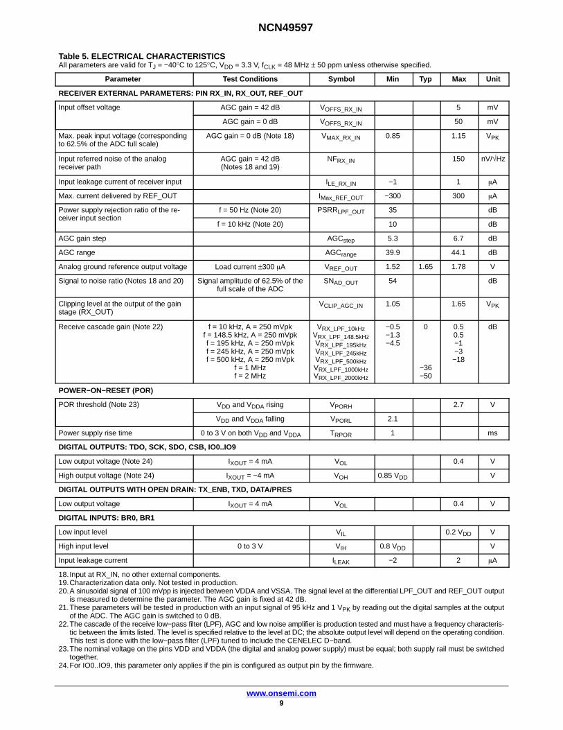
Table 5. ELECTRICAL CHARACTERISTICSAll parameters are valid for TJ = −40°C to 125°C, VDD = 3.3 V, fCLK = 48 MHz ± 50 ppm unless otherwise specified.
Parameter UnitMaxTypMinSymbolTest Conditions
RECEIVER EXTERNAL PARAMETERS: PIN RX_IN, RX_OUT, REF_OUT
Input offset voltage AGC gain = 42 dB VOFFS_RX_IN 5 mV
AGC gain = 0 dB VOFFS_RX_IN 50 mV
Max. peak input voltage (correspondingto 62.5% of the ADC full scale)
AGC gain = 0 dB (Note 18) VMAX_RX_IN 0.85 1.15 VPK
Input referred noise of the analogreceiver path
AGC gain = 42 dB(Notes 18 and 19)
NFRX_IN 150 nV/√Hz
Input leakage current of receiver input ILE_RX_IN −1 1 �A
Max. current delivered by REF_OUT IMax_REF_OUT −300 300 �A
Power supply rejection ratio of the re-ceiver input section
f = 50 Hz (Note 20) PSRRLPF_OUT 35 dB
f = 10 kHz (Note 20) 10 dB
AGC gain step AGCstep 5.3 6.7 dB
AGC range AGCrange 39.9 44.1 dB
Analog ground reference output voltage Load current ±300 �A VREF_OUT 1.52 1.65 1.78 V
Signal to noise ratio (Notes 18 and 20) Signal amplitude of 62.5% of thefull scale of the ADC
SNAD_OUT 54 dB
Clipping level at the output of the gainstage (RX_OUT)
VCLIP_AGC_IN 1.05 1.65 VPK
Receive cascade gain (Note 22) f = 10 kHz, A = 250 mVpkf = 148.5 kHz, A = 250 mVpkf = 195 kHz, A = 250 mVpkf = 245 kHz, A = 250 mVpkf = 500 kHz, A = 250 mVpk
f = 1 MHzf = 2 MHz
VRX_LPF_10kHzVRX_LPF_148.5kHzVRX_LPF_195kHzVRX_LPF_245kHzVRX_LPF_500kHzVRX_LPF_1000kHzVRX_LPF_2000kHz
−0.5−1.3−4.5
0
−36−50
0.50.5−1−3−18
dB
POWER−ON−RESET (POR)
POR threshold (Note 23) VDD and VDDA rising VPORH 2.7 V
VDD and VDDA falling VPORL 2.1
Power supply rise time 0 to 3 V on both VDD and VDDA TRPOR 1 ms
DIGITAL OUTPUTS: TDO, SCK, SDO, CSB, IO0..IO9
Low output voltage (Note 24) IXOUT = 4 mA VOL 0.4 V
High output voltage (Note 24) IXOUT = −4 mA VOH 0.85 VDD V
DIGITAL OUTPUTS WITH OPEN DRAIN: TX_ENB, TXD, DATA/PRES
Low output voltage IXOUT = 4 mA VOL 0.4 V
DIGITAL INPUTS: BR0, BR1
Low input level VIL 0.2 VDD V
High input level 0 to 3 V VIH 0.8 VDD V
Input leakage current ILEAK −2 2 �A
18.Input at RX_IN, no other external components.19.Characterization data only. Not tested in production.20.A sinusoidal signal of 100 mVpp is injected between VDDA and VSSA. The signal level at the differential LPF_OUT and REF_OUT output
is measured to determine the parameter. The AGC gain is fixed at 42 dB.21.These parameters will be tested in production with an input signal of 95 kHz and 1 VPK by reading out the digital samples at the output
of the ADC. The AGC gain is switched to 0 dB.22.The cascade of the receive low−pass filter (LPF), AGC and low noise amplifier is production tested and must have a frequency characteris-
tic between the limits listed. The level is specified relative to the level at DC; the absolute output level will depend on the operating condition.This test is done with the low−pass filter (LPF) tuned to include the CENELEC D−band.
23.The nominal voltage on the pins VDD and VDDA (the digital and analog power supply) must be equal; both supply rail must be switchedtogether.
24.For IO0..IO9, this parameter only applies if the pin is configured as output pin by the firmware.
NCN49597
www.onsemi.com10
Table 5. ELECTRICAL CHARACTERISTICSAll parameters are valid for TJ = −40°C to 125°C, VDD = 3.3 V, fCLK = 48 MHz ± 50 ppm unless otherwise specified.
Parameter UnitMaxTypMinSymbolTest Conditions
DIGITAL INPUTS WITH PULL−DOWN: TDI, TMS, TCK, TRSTB, TEST, SEN, IO8, IO9
Low input level (Note 25) VIL 0.2 VDD V
High input level (Note 25) VIH 0.8 VDD V
Pull−down resistor (Note 25) Measured at VPin = VDD / 2 RPU 35 100 170 k�
DIGITAL SCHMITT TRIGGER INPUTS: RXD, RESB, IO0..IO7, SDI
Rising threshold level (Note 26) VT+ 0.80 VDD V
Falling threshold level (Note 26) VT− 0.2 VDD V
Input leakage current (Note 26) ILEAK −2 2 �A
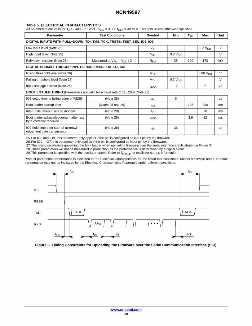
BOOT LOADER TIMING (Parameters are valid for a baud rate of 115’200) (Note 27)
IO2 setup time to falling edge of RESB (Note 28) t2s 5 �s
Boot loader startup time (Notes 28 and 29) tstx 135 200 ms
Inter−byte timeout sent to modem (Note 28) tIB 20 ms
Boot loader acknowledgement after lastbyte correctly received
(Note 28) tACK 3.6 12 ms
IO2 hold time after start of acknowl-edgement byte transmission
(Note 28) t2h 36 �s
25.For IO8 and IO9, this parameter only applies if the pin is configured as input pin by the firmware.26.For IO0…IO7, this parameter only applies if the pin is configured as input pin by the firmware.27.The timing constraints governing the boot loader when uploading firmware over the serial interface are illustrated in Figure 3.28.These parameters will not be measured in production as the performance is determined by a digital circuit.29.This parameter is specified with the oscillator stable. Refer to Tstartup for oscillator startup information.
Product parametric performance is indicated in the Electrical Characteristics for the listed test conditions, unless otherwise noted. Productperformance may not be indicated by the Electrical Characteristics if operated under different conditions.
Figure 3. Timing Constraints for Uploading the Firmware over the Serial Communication Interface (SCI)
IO2
TXD
RXD
STX ACK
RESB
tACK
t2ht2s
AAH
tstx tds tIB
NCN49597
www.onsemi.com11
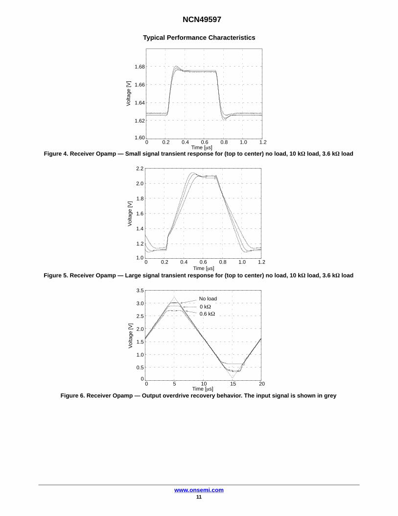
Typical Performance Characteristics
0 0.2 0.4 0.6 0.8 1.0 1.21.60
1.62
1.64
1.66
1.68
Vol
tage
[V]
Figure 4. Receiver Opamp — Small signal transient response for (top to center) no load, 10 k� load, 3.6 k� loadTime [�s]
0 0.2 0.4 0.6 0.8 1.0 1.21.0
1.2
1.4
1.6
1.8
2.0
2.2
Vol
tage
[V]
Figure 5. Receiver Opamp — Large signal transient response for (top to center) no load, 10 k� load, 3.6 k� loadTime [�s]
0 5 10 15 200
0.5
1.0
1.5
2.0
2.5
3.0
3.5
Vol
tage
[V]
Figure 6. Receiver Opamp — Output overdrive recovery behavior. The input signal is shown in greyTime [�s]
No load
0 k�0.6 k�
NCN49597
www.onsemi.com12
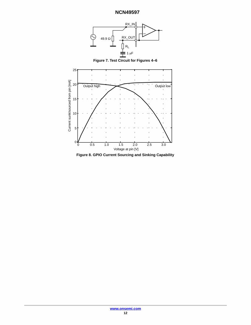
Figure 7. Test Circuit for Figures 4–6
RX_OUT
RX_IN
RL
1 �F
49.9 �
Figure 8. GPIO Current Sourcing and Sinking Capability
0 0.5 1.0 1.5 2.0 2.5 3.0Voltage at pin [V]
0
5
10
15
20
25C
urre
nt s
unk/
sour
ced
from
pin
[mA
]
Output high Output low
NCN49597
www.onsemi.com13
General Description
The NCN49597 is a single chip half duplex S−FSKmodem designed for hostile communication environmentswith very low signal−to−noise ratio (SNR) and highinterference. It is particularly suited for power line carrier(PLC) data transmission on low−or medium−voltage powerlines.
Together with firmware, the device handles of the lowerlayers of communication protocols. Firmware solutions areprovided by ON Semiconductor royalty−free for theON−PL110 protocol. It handles the physical, Media AccessControl (MAC) and Logical Link Control (LLC) layerson−chip. For more information, refer to the dedicatedsoftware datasheet.
Because the lower layers are handled on−chip, theNCN49597 provides an innovative architectural split. Theuser benefits from a higher level abstraction. Compared toa low−level interface, the NCN49597 allows fasterdevelopment of applications: the user just needs to send theraw data to the NCN49597 and no longer has to take care ofthe details of the transmission over the specific medium. Thelatter part easily represents half of the software developmentcost.
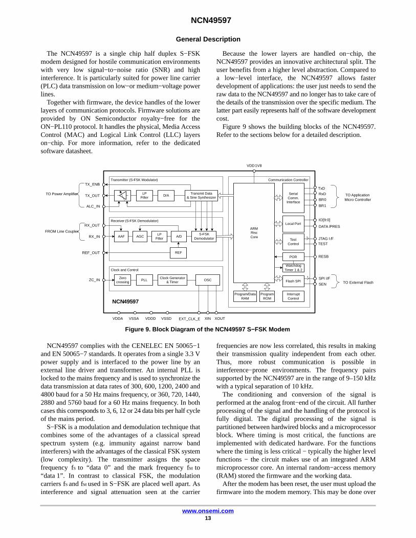
Figure 9 shows the building blocks of the NCN49597.Refer to the sections below for a detailed description.
Communication Controller
ARMRiscCore
SerialComm.
Interface
Local Port
TestControl
POR
WatchdogTimer 1 & 2
InterruptControl
Program/DataRAM
ProgramROM
S−FSKDemodulator
Receiver (S−FSK Demodulator)
Clock and Control
Zerocrossing
PLL OSCClock Generator
& Timer
Transmit Data& Sine Synthesizer
D/ALP
Filter
Transmitter (S−FSK Modulator)
RESB
JTAG I /FTEST
TX_ENB
TX_OUT
ALC_IN
RX_OUT
RX_IN
REF_OUT
ZC_IN
XIN XOUTVDDA VSSA VDDD VSSD
NCN49597
TO Power Amplifier
FROM Line Coupler
TO ApplicationMicro Controller
TxD
RxD
BR0
BR1
DATA /PRES
5
VDD1V8
IO[9:0]
SPI I/F4
EXT_CLK_E
Flash SPISEN TO External Flash
AAF AGC A/DLP
Filter
REF
Figure 9. Block Diagram of the NCN49597 S−FSK Modem
NCN49597 complies with the CENELEC EN 50065−1and EN 50065−7 standards. It operates from a single 3.3 Vpower supply and is interfaced to the power line by anexternal line driver and transformer. An internal PLL islocked to the mains frequency and is used to synchronize thedata transmission at data rates of 300, 600, 1200, 2400 and4800 baud for a 50 Hz mains frequency, or 360, 720, 1440,2880 and 5760 baud for a 60 Hz mains frequency. In bothcases this corresponds to 3, 6, 12 or 24 data bits per half cycleof the mains period.
S−FSK is a modulation and demodulation technique thatcombines some of the advantages of a classical spreadspectrum system (e.g. immunity against narrow bandinterferers) with the advantages of the classical FSK system(low complexity). The transmitter assigns the spacefrequency fS to “data 0” and the mark frequency fM to“data 1”. In contrast to classical FSK, the modulationcarriers fS and fM used in S−FSK are placed well apart. Asinterference and signal attenuation seen at the carrier
frequencies are now less correlated, this results in makingtheir transmission quality independent from each other.Thus, more robust communication is possible ininterference−prone environments. The frequency pairssupported by the NCN49597 are in the range of 9–150 kHzwith a typical separation of 10 kHz.
The conditioning and conversion of the signal isperformed at the analog front−end of the circuit. All furtherprocessing of the signal and the handling of the protocol isfully digital. The digital processing of the signal ispartitioned between hardwired blocks and a microprocessorblock. Where timing is most critical, the functions areimplemented with dedicated hardware. For the functionswhere the timing is less critical − typically the higher levelfunctions − the circuit makes use of an integrated ARMmicroprocessor core. An internal random−access memory(RAM) stored the firmware and the working data.
After the modem has been reset, the user must upload thefirmware into the modem memory. This may be done over
NCN49597
www.onsemi.com14
the asynchronous serial interface (discussed below);alternatively, the modem can autonomously retrieve thefirmware from an attached SPI memory. For details, refer tothe Boot Loader section.
The modem communicates to the applicationmicrocontroller over a Serial Communication Interface(SCI), a standard asynchronous serial link, which allowsinterfacing with any microcontroller with a free UART. TheSCI works on two wires: TXD and RXD. The baud rate isprogrammed by setting two pins (BR0, BR1).
The NCN49597, together with an NCS5651 line driver, isfunctionally equivalent to the NCN49599 modem. Thus, thesame user software works equally well with the NCN49597as with the NCN49599.
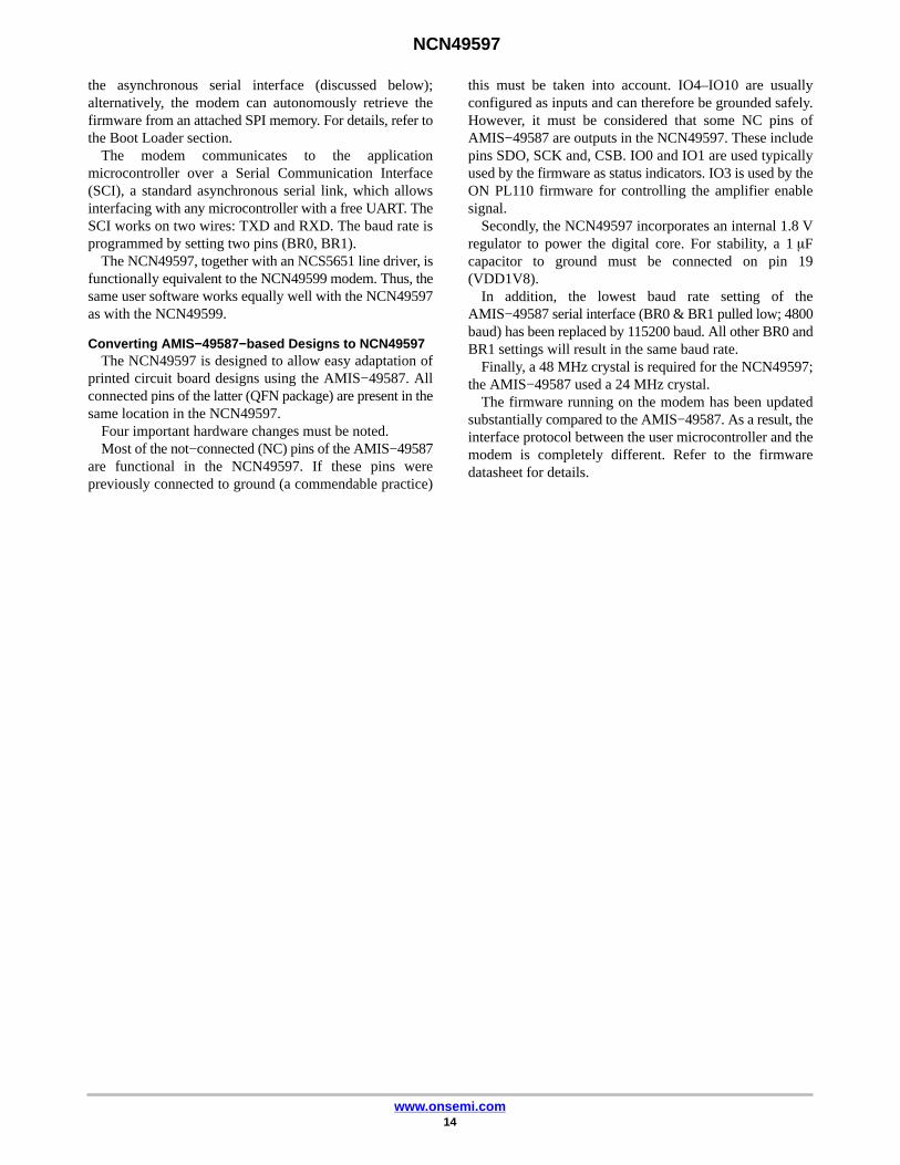
Converting AMIS−49587−based Designs to NCN49597The NCN49597 is designed to allow easy adaptation of
printed circuit board designs using the AMIS−49587. Allconnected pins of the latter (QFN package) are present in thesame location in the NCN49597.
Four important hardware changes must be noted.Most of the not−connected (NC) pins of the AMIS−49587
are functional in the NCN49597. If these pins werepreviously connected to ground (a commendable practice)
this must be taken into account. IO4–IO10 are usuallyconfigured as inputs and can therefore be grounded safely.However, it must be considered that some NC pins ofAMIS−49587 are outputs in the NCN49597. These includepins SDO, SCK and, CSB. IO0 and IO1 are used typicallyused by the firmware as status indicators. IO3 is used by theON PL110 firmware for controlling the amplifier enablesignal.
Secondly, the NCN49597 incorporates an internal 1.8 Vregulator to power the digital core. For stability, a 1 �Fcapacitor to ground must be connected on pin 19(VDD1V8).
In addition, the lowest baud rate setting of theAMIS−49587 serial interface (BR0 & BR1 pulled low; 4800baud) has been replaced by 115200 baud. All other BR0 andBR1 settings will result in the same baud rate.
Finally, a 48 MHz crystal is required for the NCN49597;the AMIS−49587 used a 24 MHz crystal.
The firmware running on the modem has been updatedsubstantially compared to the AMIS−49587. As a result, theinterface protocol between the user microcontroller and themodem is completely different. Refer to the firmwaredatasheet for details.
NCN49597
www.onsemi.com15
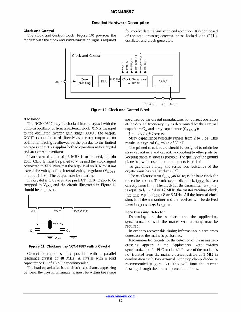
Detailed Hardware Description
Clock and ControlThe clock and control block (Figure 10) provides the
modem with the clock and synchronization signals required
for correct data transmission and reception. It is composedof the zero−crossing detector, phase locked loop (PLL),oscillator and clock generator.
Clock and Control
Zerocrossing PLL
Clock Generator& TimerZC_IN
XIN XOUT
BIT_
CLK
BYTE
_CLK
FRAM
E_C
LK
PRE
_BYT
E_C
LK
PRE
_FR
AM
E_C
LK
PRE
_SLO
T
CHIP_CLK
EXT_CLK_E
OSC
Figure 10. Clock and Control Block
OscillatorThe NCN49597 may be clocked from a crystal with the
built−in oscillator or from an external clock. XIN is the inputto the oscillator inverter gain stage; XOUT the output.XOUT cannot be used directly as a clock output as noadditional loading is allowed on the pin due to the limitedvoltage swing. This applies both to operation with a crystaland an external oscillator.
If an external clock of 48 MHz is to be used, the pinEXT_CLK_E must be pulled to VDD and the clock signalconnected to XIN. Note that the high level on XIN must notexceed the voltage of the internal voltage regulator (VDD18,or about 1.8 V). The output must be floating.
If a crystal is to be used, the pin EXT_CLK_E should bestrapped to VSSA and the circuit illustrated in Figure 11should be employed.
XIN XOUT
CX
VSSA
CX
48 MHz
EXT_CLK_E
Figure 11. Clocking the NCN49597 with a Crystal
Correct operation is only possible with a parallelresonance crystal of 48 MHz. A crystal with a loadcapacitance CL of 18 pF is recommended.
The load capacitance is the circuit capacitance appearingbetween the crystal terminals; it must be within the range
specified by the crystal manufacturer for correct operationat the desired frequency. CL is determined by the externalcapacitors CX and stray capacitance (CSTRAY):
CL = CX / 2 + CSTRAYStray capacitance typically ranges from 2 to 5 pF. This
results in a typical CX value of 33 pF.The printed circuit board should be designed to minimize
stray capacitance and capacitive coupling to other parts bykeeping traces as short as possible. The quality of the groundplane below the oscillator components is critical.
To guarantee startup, the series loss resistance of thecrystal must be smaller than 60 �.
The oscillator output fCLK (48 MHz) is the base clock forthe entire modem. The microcontroller clock, fARM, is takendirectly from fCLK. The clock for the transmitter, fTX_CLK,is equal to fCLK / 4 or 12 MHz; the master receiver clock,fRX_CLK, equals fCLK / 8 or 6 MHz. All the internal clocksignals of the transmitter and the receiver will be derivedfrom fTX_CLK resp. fRX_CLK..
Zero Crossing DetectorDepending on the standard and the application,
synchronization with the mains zero crossing may berequired.
In order to recover this timing information, a zero crossdetection of the mains is performed.
Recommended circuits for the detection of the mains zerocrossing appear in the Application Note “Mainssynchronization for PLC modems”. In case of the modem isnot isolated from the mains a series resistor of 1 M� incombination with two external Schottky clamp diodes isrecommended (Figure 12). This will limit the currentflowing through the internal protection diodes.
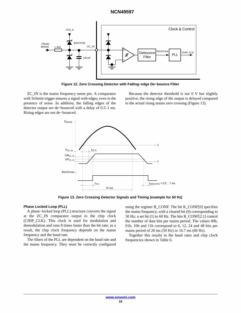
NCN49597
www.onsemi.com16
FROMMAINS
Clock & Control
ZC_IN
ZeroCross
PLLCHIP_CLKDebounce
Filter
3V3_A
1 M�
100 pF
BAS70−04
Figure 12. Zero Crossing Detector with Falling−edge De−bounce Filter
ZC_IN is the mains frequency sense pin. A comparatorwith Schmitt trigger ensures a signal with edges, even in thepresence of noise. In addition, the falling edges of thedetector output are de−bounced with a delay of 0.5–1 ms.Rising edges are not de−bounced.
Because the detector threshold is not 0 V but slightlypositive, the rising edge of the output is delayed comparedto the actual rising mains zero crossing (Figure 13).
Figure 13. Zero Crossing Detector Signals and Timing (example for 50 Hz)
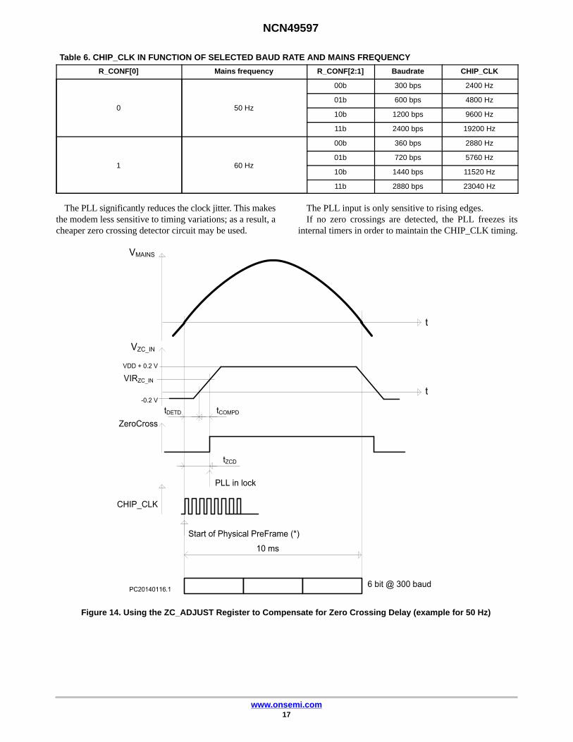
Phase Locked Loop (PLL)A phase−locked loop (PLL) structure converts the signal
at the ZC_IN comparator output to the chip clock(CHIP_CLK). This clock is used for modulation anddemodulation and runs 8 times faster than the bit rate; as aresult, the chip clock frequency depends on the mainsfrequency and the baud rate.
The filters of the PLL are dependent on the baud rate andthe mains frequency. They must be correctly configured
using the register R_CONF. The bit R_CONF[0] specifiesthe mains frequency, with a cleared bit (0) corresponding to50 Hz; a set bit (1) to 60 Hz. The bits R_CONF[2:1] controlthe number of data bits per mains period. The values 00b,01b, 10b and 11b correspond to 6, 12, 24 and 48 bits permains period of 20 ms (50 Hz) or 16.7 ms (60 Hz).
Together this results in the baud rates and chip clockfrequencies shown in Table 6.
NCN49597
www.onsemi.com17
Table 6. CHIP_CLK IN FUNCTION OF SELECTED BAUD RATE AND MAINS FREQUENCY
R_CONF[0] Mains frequency R_CONF[2:1] Baudrate CHIP_CLK
0 50 Hz
00b 300 bps 2400 Hz
01b 600 bps 4800 Hz
10b 1200 bps 9600 Hz
11b 2400 bps 19200 Hz
1 60 Hz
00b 360 bps 2880 Hz
01b 720 bps 5760 Hz
10b 1440 bps 11520 Hz
11b 2880 bps 23040 Hz
The PLL significantly reduces the clock jitter. This makesthe modem less sensitive to timing variations; as a result, acheaper zero crossing detector circuit may be used.
The PLL input is only sensitive to rising edges.If no zero crossings are detected, the PLL freezes its
internal timers in order to maintain the CHIP_CLK timing.
Figure 14. Using the ZC_ADJUST Register to Compensate for Zero Crossing Delay (example for 50 Hz)
NCN49597
www.onsemi.com18
The PLL ensures the generated chip clock is in phase withthe rising edge of comparator output. However, these edgesare not precisely in phase with the mains.
Inevitably, the external zero crossing detector circuitsuffers from a delay tDETD (e.g. caused by an optocoupler).In addition, the comparator threshold is not zero (VIRZC_IN= 1.9 V); this results in a further delay, tCOMP0 between therising edge of the signal on pin ZC_IN and the rising edgeon the comparator output (as noted before, the PLL takesonly the rising edge into account).
The combination of these delays would cause the modemto emit and receive data frames too late.
Therefore, the PLL allows tuning the phase differencebetween its input and the chip clock. The CHIP_CLK maybe brought forward by setting the register R_ZC_ADJUST.The adjustment period or granularity is 13 �s, with amaximum adjustment of 255 x 13 �s = 3.3 ms,corresponding with a sixth of the 50 Hz mains sine period.
This is illustrated in Figure 9. The “physical frame” (i.e.,the modulated signal appearing on the mains) starts earlierwith R_ZC_ADJUST[7:0] x 13 �s to compensate for thezero cross delay.
The delay corresponding with the value ofR_ZC_ADJUST is also listed in Table 7.
Table 7. ZERO CROSSING DELAY COMPENSATION
R_ZC_ADJUST[7:0] Compensation
0000 0000 0 �s (reset value)
0000 0001 13 �s
0000 0010 26 �s
0000 0011 39 �s
... ...
1111 1111 3315 �s
Clock Generator and TimerThe timing generator (Figure 10, center) is responsible for
all synchronization signals and interrupts related to S−FSKcommunication.
The timing is derived from the chip clock (CHIP_CLK,generated by the PLL) and the main oscillator clock fCLK.The timing has a fixed repetition rate, corresponding to thelength of a physical subframe (see reference [1]).
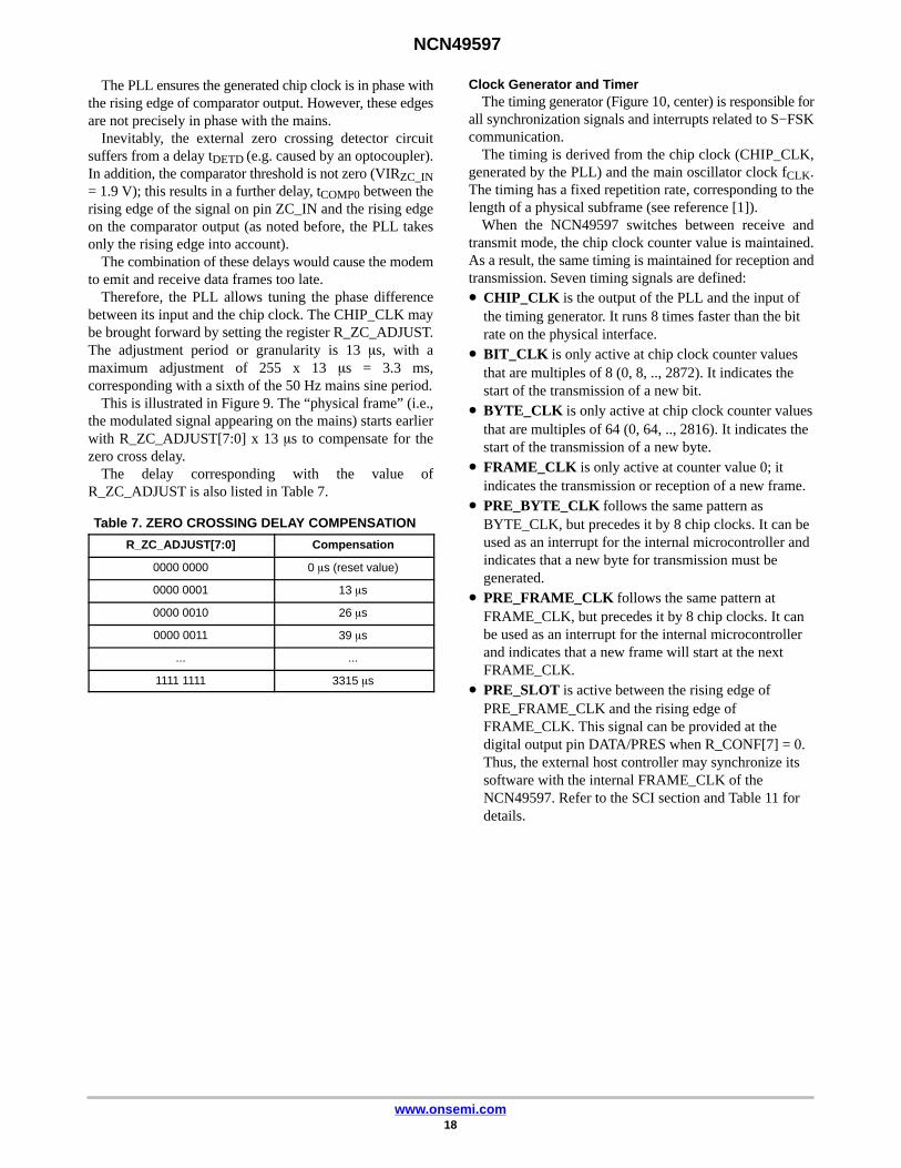
When the NCN49597 switches between receive andtransmit mode, the chip clock counter value is maintained.As a result, the same timing is maintained for reception andtransmission. Seven timing signals are defined:• CHIP_CLK is the output of the PLL and the input of
the timing generator. It runs 8 times faster than the bitrate on the physical interface.
• BIT_CLK is only active at chip clock counter valuesthat are multiples of 8 (0, 8, .., 2872). It indicates thestart of the transmission of a new bit.
• BYTE_CLK is only active at chip clock counter valuesthat are multiples of 64 (0, 64, .., 2816). It indicates thestart of the transmission of a new byte.
• FRAME_CLK is only active at counter value 0; itindicates the transmission or reception of a new frame.
• PRE_BYTE_CLK follows the same pattern asBYTE_CLK, but precedes it by 8 chip clocks. It can beused as an interrupt for the internal microcontroller andindicates that a new byte for transmission must begenerated.
• PRE_FRAME_CLK follows the same pattern atFRAME_CLK, but precedes it by 8 chip clocks. It canbe used as an interrupt for the internal microcontrollerand indicates that a new frame will start at the nextFRAME_CLK.
• PRE_SLOT is active between the rising edge ofPRE_FRAME_CLK and the rising edge ofFRAME_CLK. This signal can be provided at thedigital output pin DATA/PRES when R_CONF[7] = 0.Thus, the external host controller may synchronize itssoftware with the internal FRAME_CLK of theNCN49597. Refer to the SCI section and Table 11 fordetails.
NCN49597
www.onsemi.com19
BIT_CLK
63 64 652871 2872 102879 2 3 4 5 6 7 8 9
CHIP_CLK
BYTE_CLK
FRAME _CLK
PRE_FRAME _CLK
PRE_BYTE_CLK
R_CHIP_CNT
PRE_SLOT
Start of the physical subframe
Figure 15. Timing Signals
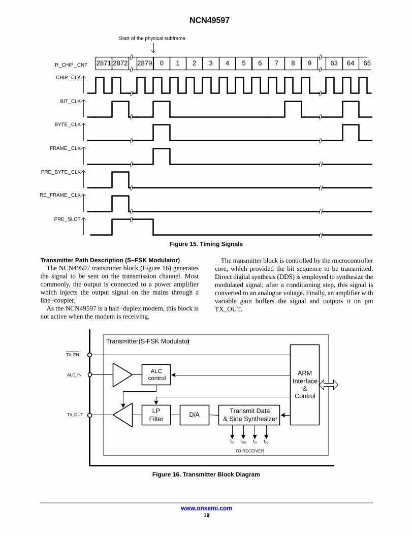
Transmitter Path Description (S−FSK Modulator)The NCN49597 transmitter block (Figure 16) generates
the signal to be sent on the transmission channel. Mostcommonly, the output is connected to a power amplifierwhich injects the output signal on the mains through aline−coupler.
As the NCN49597 is a half−duplex modem, this block isnot active when the modem is receiving.
The transmitter block is controlled by the microcontrollercore, which provided the bit sequence to be transmitted.Direct digital synthesis (DDS) is employed to synthesize themodulated signal; after a conditioning step, this signal isconverted to an analogue voltage. Finally, an amplifier withvariable gain buffers the signal and outputs it on pinTX_OUT.
Transmitter(S−FSK Modulator)
ARMInterface
&Control
TX_OUTTransmit Data
& Sine SynthesizerD/A
LPFilter
ALCcontrol
ALC_IN
TO RECEIVER
fMI fMQ fSI fSQ
TX_EN
Figure 16. Transmitter Block Diagram
NCN49597
www.onsemi.com20
Microcontroller Interface & ControlThe interface with the internal ARM microcontroller
consists of an 8−bit data register R_TX_DATA, 2 controlregisters R_TX_CTRL and R_ALC_CTRL, a flagTX_RXB defining the operating mode (a high levelcorresponding to transmit mode; low to receive) and thefrequency control registers. All these registers are memorymapped; most can be accessed through the firmware: referto the specific firmware documentation for details.
Sine Wave GeneratorThe direct digital synthesizer (DDS) generates a
sinusoidal signal alternating between the space frequency(fS, data 0) and the mark frequency (fM, data 1) as requiredto modulate the desired bit pattern. Two 16−bit widefrequency step registers, R_FM and R_FS, control the stepsused by the DDS and thus the frequencies.
The space and mark frequency can be calculated usingfS = R_FS[15:0]_dec • fDDS/218
fM = R_FM[15:0]_dec • fDDS/218
Equivalently, values for R_FS[15:0] and R_FM[15:0]may be calculated from the desired carrier frequencies
R_FS[15:0]_dec = [218 • fS/fDDS]R_FM[15:0]_dec = [218 • fM/fDDS]
With fDDS = 3 MHz the direct digital synthesizer clockfrequency and [x] equal to x rounded to the nearest integer.
At the start of the transmission the DDS phaseaccumulator starts at 0, resulting in a 0 V output level.Switching between fM and fS is phase−continuous. Uponswitching to receive mode the DDS completes the activesine period. These precautions minimize spurious emissions.
DA Converter and Anti−aliasing FilterA digital to analogue ΣΔ converter converts the sine wave
digital word to a pulse density modulated (PDM) signal. ThePDM stream is converted to an analogue signal with a firstorder switched capacitor filter.
A 3rd order continuous time low pass filter in the transmitpath filters the quantization noise and noise generated by theΣΔ DA converter.
The −3 dB frequency of this filter can be set to 130 kHz forapplications using the CENELEC A band. In thisconfiguration, the response of the filter is virtually flat up to95 kHz. Alternatively a −3 dB frequency of 195 kHz can beselected yielding a flat response for the entire CENELEC Ato D band (i.e., up to 148.5 kHz). Refer to the documentationof the firmware for more information.
The low pass filter is tuned automatically to compensatefor process variation.
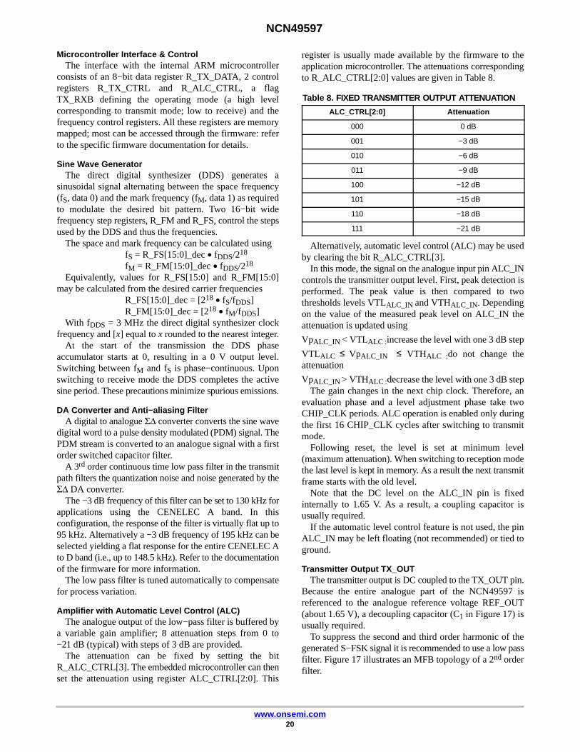
Amplifier with Automatic Level Control (ALC)The analogue output of the low−pass filter is buffered by
a variable gain amplifier; 8 attenuation steps from 0 to−21 dB (typical) with steps of 3 dB are provided.
The attenuation can be fixed by setting the bitR_ALC_CTRL[3]. The embedded microcontroller can thenset the attenuation using register ALC_CTRL[2:0]. This
register is usually made available by the firmware to theapplication microcontroller. The attenuations correspondingto R_ALC_CTRL[2:0] values are given in Table 8.
Table 8. FIXED TRANSMITTER OUTPUT ATTENUATION
ALC_CTRL[2:0] Attenuation
000 0 dB
001 −3 dB
010 −6 dB
011 −9 dB
100 −12 dB
101 −15 dB
110 −18 dB
111 −21 dB
Alternatively, automatic level control (ALC) may be usedby clearing the bit R_ALC_CTRL[3].
In this mode, the signal on the analogue input pin ALC_INcontrols the transmitter output level. First, peak detection isperformed. The peak value is then compared to twothresholds levels VTLALC_IN and VTHALC_IN. Dependingon the value of the measured peak level on ALC_IN theattenuation is updated using
VpALC_IN < VTLALC :increase the level with one 3 dB step
VTLALC ≤ VpALC_IN ≤ VTHALC :do not change theattenuation
VpALC_IN > VTHALC :decrease the level with one 3 dB stepThe gain changes in the next chip clock. Therefore, an
evaluation phase and a level adjustment phase take twoCHIP_CLK periods. ALC operation is enabled only duringthe first 16 CHIP_CLK cycles after switching to transmitmode.
Following reset, the level is set at minimum level(maximum attenuation). When switching to reception modethe last level is kept in memory. As a result the next transmitframe starts with the old level.
Note that the DC level on the ALC_IN pin is fixedinternally to 1.65 V. As a result, a coupling capacitor isusually required.
If the automatic level control feature is not used, the pinALC_IN may be left floating (not recommended) or tied toground.
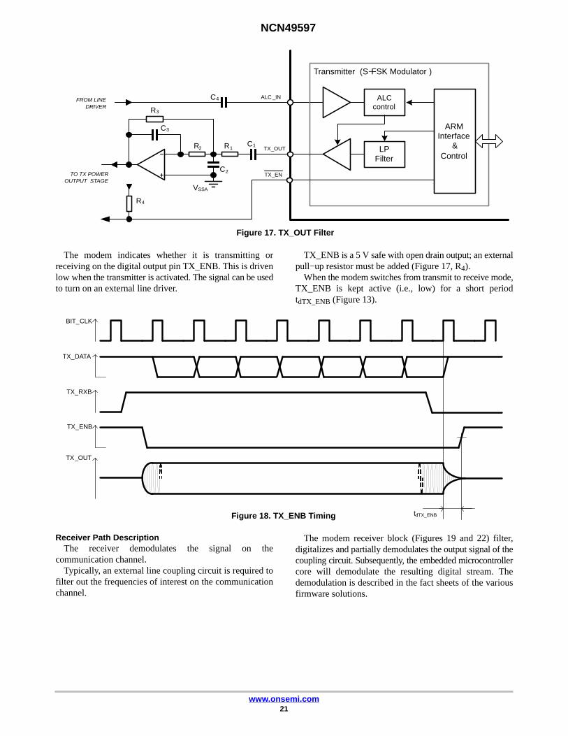
Transmitter Output TX_OUTThe transmitter output is DC coupled to the TX_OUT pin.
Because the entire analogue part of the NCN49597 isreferenced to the analogue reference voltage REF_OUT(about 1.65 V), a decoupling capacitor (C1 in Figure 17) isusually required.
To suppress the second and third order harmonic of thegenerated S−FSK signal it is recommended to use a low passfilter. Figure 17 illustrates an MFB topology of a 2nd orderfilter.
NCN49597
www.onsemi.com21
ALCcontrol
ALC _IN
Transmitter (S−FSK Modulator )
ARMInterface
&Control
TX_OUT LPFilter
TX_ENTO TX POWEROUTPUT STAGE
FROM LINEDRIVER
C1R1
VSSA
C2
R2
R3
C3
C4
R4
Figure 17. TX_OUT Filter
The modem indicates whether it is transmitting orreceiving on the digital output pin TX_ENB. This is drivenlow when the transmitter is activated. The signal can be usedto turn on an external line driver.
TX_ENB is a 5 V safe with open drain output; an externalpull−up resistor must be added (Figure 17, R4).
When the modem switches from transmit to receive mode,TX_ENB is kept active (i.e., low) for a short periodtdTX_ENB (Figure 13).
TX_DATA
TX_RXB
tdTX_ENB
BIT_CLK
TX_ENB
TX_OUT
Figure 18. TX_ENB Timing
Receiver Path DescriptionThe receiver demodulates the signal on the
communication channel.Typically, an external line coupling circuit is required to
filter out the frequencies of interest on the communicationchannel.
The modem receiver block (Figures 19 and 22) filter,digitalizes and partially demodulates the output signal of thecoupling circuit. Subsequently, the embedded microcontrollercore will demodulate the resulting digital stream. Thedemodulation is described in the fact sheets of the variousfirmware solutions.

NCN49597
www.onsemi.com22
RX_OUT
RX_IN
REF_OUT
LOW NOISEOPAMP
REF1,65 V
TODIGITAL
Receiver(Analog Path)
Gain LPF4th
order�� AD
FROMDIGITAL
Figure 19. Analog Path of the Receiver Block
Absvalueaccu
Receiver (Digital Path)
1st
DecimatorNoise
ShaperCompen−
sator
AGCControl
FROMANALOG
TOGAIN
fSI
fMQ
fSQ
SlidingFilter
SlidingFilter
SlidingFilter
SlidingFilter
Quadrature Demodulator
fS
fM
2nd
Decimator
2nd
Decimator
2nd
Decimator
2nd
Decimator
IM
QM
IS
QS
fMI
FROM TRANSMITTER
fMQ fSI fSQ
Figure 20. Digital Path of the Receiver Block
The receiver block is composed of an operation amplifierprovided for filtering, a variable gain amplifier, ananti−aliasing low pass filter and analogue to digitalconvertor (ADC), and a digital quadrature downmixer.
When the modem is transmitting, the receive blocks aredisabled to save power. The only exception is the low−passfilter, which is shared between receiver and transmitter andtherefore remains active.
50/60 Hz Suppression FilterThe line coupler − external to the modem and not
described in this document − couples the communicationchannel to the low−voltage signal input of the modem.Ideally the signal produced by the line coupler would onlycontain the frequency band used by the S−FSK modulation.
For the common case of communication over an AC powerline, a substantial 50 or 60 Hz residue is still present after theline coupler. This residue − typically much larger than thereceived signal − can easily overload the modem.
To improve communication performance, the NCN49597provides a low−noise operational amplifier in a unity−gainconfiguration which can be used to make a 50/60 Hzsuppression filter with only four external passivecomponents. Pin RX_IN is the non−inverting input andRX_OUT is the output of the amplifier.
The internal reference voltage (described below) of1.65 V is provided on REF_OUT and can be used for thispurpose. The current drawn from this pin should be limitedto 300 �A; in addition, adding a ceramic decouplingcapacitor of at least 1 �F is recommended.
C1
R1
C2
R2
CDREF
RX_OUT
RX_IN
REF_OUT
ReceivedSignal
VSSA
LOW NOISEOPAMP
REF1,65 V
TO AGC
Receiver (S−FSK Demodulator)
VIN
Figure 21. External Component Connection for 50/60 Hz Suppression Filter
NCN49597
www.onsemi.com23
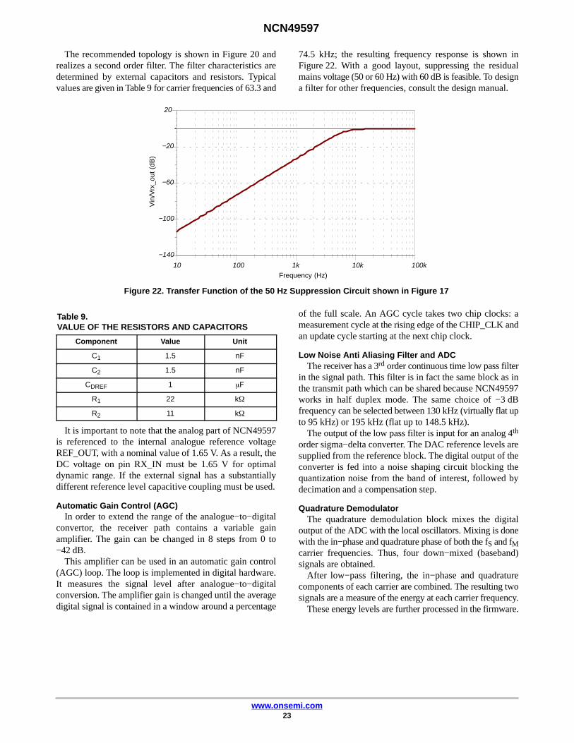
The recommended topology is shown in Figure 20 andrealizes a second order filter. The filter characteristics aredetermined by external capacitors and resistors. Typicalvalues are given in Table 9 for carrier frequencies of 63.3 and
74.5 kHz; the resulting frequency response is shown inFigure 22. With a good layout, suppressing the residualmains voltage (50 or 60 Hz) with 60 dB is feasible. To designa filter for other frequencies, consult the design manual.
T
Frequency (Hz)
10 100 1k 10k 100k
Vin
/Vrx
_out
(dB
)
−140
−100
−60
−20
20
Figure 22. Transfer Function of the 50 Hz Suppression Circuit shown in Figure 17
Table 9. VALUE OF THE RESISTORS AND CAPACITORS
Component Value Unit
C1 1.5 nF
C2 1.5 nF
CDREF 1 �F
R1 22 k�
R2 11 k�
It is important to note that the analog part of NCN49597is referenced to the internal analogue reference voltageREF_OUT, with a nominal value of 1.65 V. As a result, theDC voltage on pin RX_IN must be 1.65 V for optimaldynamic range. If the external signal has a substantiallydifferent reference level capacitive coupling must be used.
Automatic Gain Control (AGC)In order to extend the range of the analogue−to−digital
convertor, the receiver path contains a variable gainamplifier. The gain can be changed in 8 steps from 0 to−42 dB.
This amplifier can be used in an automatic gain control(AGC) loop. The loop is implemented in digital hardware.It measures the signal level after analogue−to−digitalconversion. The amplifier gain is changed until the averagedigital signal is contained in a window around a percentage
of the full scale. An AGC cycle takes two chip clocks: ameasurement cycle at the rising edge of the CHIP_CLK andan update cycle starting at the next chip clock.
Low Noise Anti Aliasing Filter and ADCThe receiver has a 3rd order continuous time low pass filter
in the signal path. This filter is in fact the same block as inthe transmit path which can be shared because NCN49597works in half duplex mode. The same choice of −3 dBfrequency can be selected between 130 kHz (virtually flat upto 95 kHz) or 195 kHz (flat up to 148.5 kHz).
The output of the low pass filter is input for an analog 4th
order sigma−delta converter. The DAC reference levels aresupplied from the reference block. The digital output of theconverter is fed into a noise shaping circuit blocking thequantization noise from the band of interest, followed bydecimation and a compensation step.
Quadrature DemodulatorThe quadrature demodulation block mixes the digital
output of the ADC with the local oscillators. Mixing is donewith the in−phase and quadrature phase of both the fS and fMcarrier frequencies. Thus, four down−mixed (baseband)signals are obtained.
After low−pass filtering, the in−phase and quadraturecomponents of each carrier are combined. The resulting twosignals are a measure of the energy at each carrier frequency.
These energy levels are further processed in the firmware.
NCN49597
www.onsemi.com24
Communication ControllerThe Communication Controller block includes the micro−processor and its peripherals (refer to Figure 23 for an overview).
Communication Controller
ARMRiscCore
POR
Watchdog
Timer 1 & 2
InterruptControl
ProgramROM
RESBFROMRECEIVER
TOTRANSMIT
Flash SPI
SerialComm.
Interface
TxD
RxD
BR0
BR1
Local PortIO[9:0]
DATA /PRES
TESTTest
Control
CS
B
SD
O
SD
I
Data / ProgramRAM
SE
N
SC
K
Figure 23. The Communication Controller is Based on a Standard ARM Corex M0 Core
The processor is an ARM Cortex M0 32−bit core with areduced instruction set computer (RISC) architecture,optimized for IO handling. Most instructions complete in asingle clock cycle, including byte multiplication. Theperipherals include a watchdog, test and debug control,RAM, ROM containing the boot loader, UART, two timers,an SPI interface to optional external memory, I/O ports andthe power−on reset. The microcontroller implementsinterrupts.
The 32 kB RAM contains the necessary space to store thefirmware and the working data. A full−duplex serialcommunication block allows interfacing to the applicationmicrocontroller.
Local PortTen bidirectional general purpose input/output (GPIO)
pins (IO0..IO9) are provided. All general purpose IO pinscan be configured as an input or an output. In addition, thefirmware can emulate open−drain or open−source pins. Allpins are 5 V tolerant.
When the modem is booting, IO2 is configured as an inputand must be pulled low to enable uploading firmware overthe serial interface. At the same time, IO0 and IO1 areconfigured as outputs and show the status of the boot loader.A LED may be connected to IO0 to help with debugging.After the firmware has been loaded successfully, IO0..IO2become available as normal IOs.
Typically, the firmware provides status indication onsome IO pins; other IO pins remain available to theapplication microcontroller as IO extensions.
The application microcontroller has also low−level accessto internal timing of the modem through the digital outputDATA/PRES pin. The function of this pin depends on theregister bit R_CONF[7].
If the bit is cleared (0), the preslot synchronization signal(PRE_SLOT) appears on the pin.
If the bit is set (1), the modem outputs the baseband,unmodulated, data. Thus, DATA/PRES is driven high whena space symbol is being transmitted (i.e., the spacefrequency fS appears on pin TX_OUT); it is driven low whena mask symbol is transmitted (fM on TX_OUT).
TestingA JTAG debug interface is provided for development,
debugging and production test. An internal pull−downresistor is provided on the input pins (TDI, TCK, TMS, andTRSTB).
In practice, the end user of the modem will not need thisinterface; this input pins may be tied to ground(recommended) or left floating; TDO should be left floating.
The pin TEST enables the internal hardware test modewhen driven high. During normal operation, it should be tiedto ground (recommended) or left floating.
Serial Communication Interface (SCI)The Serial Communication Interface allows
asynchronous communication with any deviceincorporating a standard Universal Asynchronous ReceiverTransmitter (UART).

NCN49597
www.onsemi.com25
The serial interface is full−duplex and uses the standard NRZ format with a single start bit, eight data bits and one stop bit(Figure 24). The baud rate is programmable from 9600 to 115200 baud through the BR0 and BR1 pins.
tBIT
IDLE (mark) LSB MSB IDLE(mark)
tBIT8 data bits
1 characterPC20080523.3
D0Start D1 D2 D3 D4 D5 D6 D7 Stop
Figure 24. Data Format of the Serial Interface
Serial data is sent from the NCN49597 to the applicationmicrocontroller on pin TxD; data is received on pin RxD.Both pins are 5 V tolerant, allowing communication withboth 3.3 V−and 5 V−powered devices.
On the open−drain output pin TxD an external pull−upresistor must be provided to define the logic high level(Figure 25). A value of 10 k� is recommended. Dependingon the application, an external pull−up resistor on RxD maybe required to avoid a floating input.
VSSD
+5V
Output
R
Figure 25. Interfacing to 5 V Logic using a 5 V SafeOutput and a Pull−up Resistor
Communication Controller
ARMRiscCore
SerialComm.
Interface
TxD
RxD
BR0BR1
Local PortIO[9:0]DATA /PRES
NCN49597
ApplicationMicro
Controller
3V3_D
Figure 26. Connection to the Application Microcontroller
The baud rate of the serial communication is controlled bythe pins BR0 and BR1. After reset, the logic level on thesepins is read and latched; as a result, modification of the baudrate during operation is not possible. The baud rate derivedfrom BR0 and BR1 is shown in Table 10.
Table 10. BR1, BR0 BAUD RATES
BR1 BR0 SCI Baud Rate
0 0 115200
0 1 9600
1 0 19200
1 1 38400
BR0 and BR1 are 5 V safe, allowing direct connection to5 V−powered logic.
NCN49597
www.onsemi.com26
WatchdogA watchdog supervises the ARM microcontroller. In case
the firmware does not periodically signal the watchdog it isalive, it is assumed an error has occurred and a hard reset isgenerated.
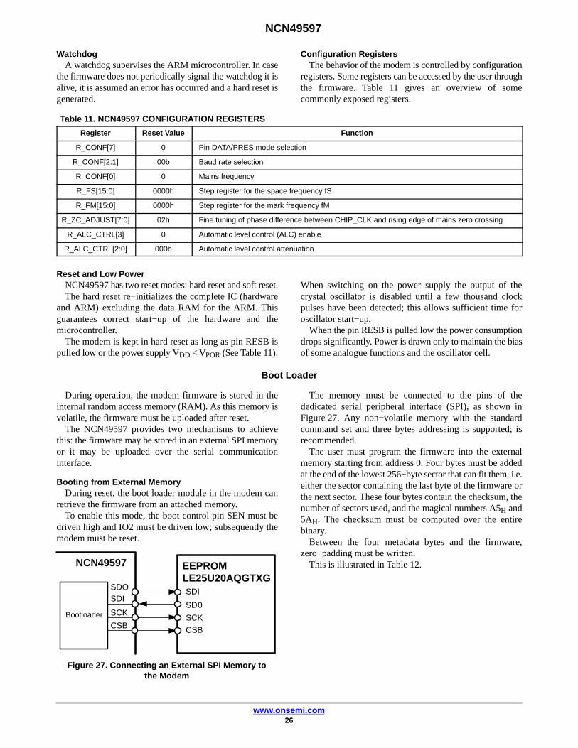
Configuration RegistersThe behavior of the modem is controlled by configuration
registers. Some registers can be accessed by the user throughthe firmware. Table 11 gives an overview of somecommonly exposed registers.
Table 11. NCN49597 CONFIGURATION REGISTERS
Register Reset Value Function
R_CONF[7] 0 Pin DATA/PRES mode selection
R_CONF[2:1] 00b Baud rate selection
R_CONF[0] 0 Mains frequency
R_FS[15:0] 0000h Step register for the space frequency fS
R_FM[15:0] 0000h Step register for the mark frequency fM
R_ZC_ADJUST[7:0] 02h Fine tuning of phase difference between CHIP_CLK and rising edge of mains zero crossing
R_ALC_CTRL[3] 0 Automatic level control (ALC) enable
R_ALC_CTRL[2:0] 000b Automatic level control attenuation
Reset and Low PowerNCN49597 has two reset modes: hard reset and soft reset.The hard reset re−initializes the complete IC (hardware
and ARM) excluding the data RAM for the ARM. Thisguarantees correct start−up of the hardware and themicrocontroller.
The modem is kept in hard reset as long as pin RESB ispulled low or the power supply VDD < VPOR (See Table 11).
When switching on the power supply the output of thecrystal oscillator is disabled until a few thousand clockpulses have been detected; this allows sufficient time foroscillator start−up.
When the pin RESB is pulled low the power consumptiondrops significantly. Power is drawn only to maintain the biasof some analogue functions and the oscillator cell.
Boot Loader
During operation, the modem firmware is stored in theinternal random access memory (RAM). As this memory isvolatile, the firmware must be uploaded after reset.
The NCN49597 provides two mechanisms to achievethis: the firmware may be stored in an external SPI memoryor it may be uploaded over the serial communicationinterface.
Booting from External MemoryDuring reset, the boot loader module in the modem can
retrieve the firmware from an attached memory.To enable this mode, the boot control pin SEN must be
driven high and IO2 must be driven low; subsequently themodem must be reset.
Bootloader
SDO
NCN49597
SDI
SCK
SDI
SD0
SCK
EEPROMLE25U20AQGTXG
CSB CSB
Figure 27. Connecting an External SPI Memory tothe Modem
The memory must be connected to the pins of thededicated serial peripheral interface (SPI), as shown inFigure 27. Any non−volatile memory with the standardcommand set and three bytes addressing is supported; isrecommended.
The user must program the firmware into the externalmemory starting from address 0. Four bytes must be addedat the end of the lowest 256−byte sector that can fit them, i.e.either the sector containing the last byte of the firmware orthe next sector. These four bytes contain the checksum, thenumber of sectors used, and the magical numbers A5H and5AH. The checksum must be computed over the entirebinary.
Between the four metadata bytes and the firmware,zero−padding must be written.
This is illustrated in Table 12.
NCN49597
www.onsemi.com27
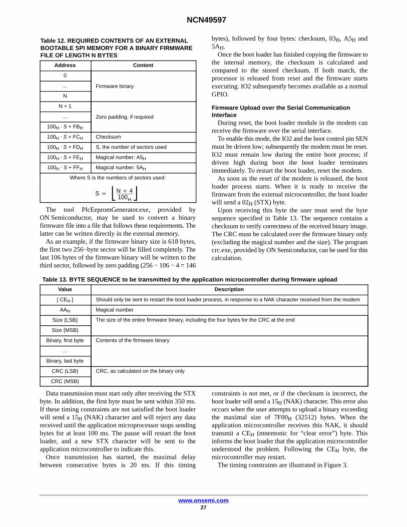
Table 12. REQUIRED CONTENTS OF AN EXTERNALBOOTABLE SPI MEMORY FOR A BINARY FIRMWAREFILE OF LENGTH N BYTES
Address Content
0
Firmware binary...
N
N + 1
Zero padding, if required...
100H � S + FBH
100H � S + FCH Checksum
100H � S + FDH S, the number of sectors used
100H � S + FEH Magical number: A5H
100H � S + FFH Magical number: 5AH
Where S is the numbers of sectors used:
S ��N � 4100H
�The tool PlcEepromGenerator.exe, provided by
ON Semiconductor, may be used to convert a binaryfirmware file into a file that follows these requirements. Thelatter can be written directly in the external memory.
As an example, if the firmware binary size is 618 bytes,the first two 256−byte sector will be filled completely. Thelast 106 bytes of the firmware binary will be written to thethird sector, followed by zero padding (256 − 106 − 4 = 146
bytes), followed by four bytes: checksum, 03H, A5H and5AH.
Once the boot loader has finished copying the firmware tothe internal memory, the checksum is calculated andcompared to the stored checksum. If both match, theprocessor is released from reset and the firmware startsexecuting. IO2 subsequently becomes available as a normalGPIO.
Firmware Upload over the Serial CommunicationInterface
During reset, the boot loader module in the modem canreceive the firmware over the serial interface.
To enable this mode, the IO2 and the boot control pin SENmust be driven low; subsequently the modem must be reset.IO2 must remain low during the entire boot process; ifdriven high during boot the boot loader terminatesimmediately. To restart the boot loader, reset the modem.
As soon as the reset of the modem is released, the bootloader process starts. When it is ready to receive thefirmware from the external microcontroller, the boot loaderwill send a 02H (STX) byte.
Upon receiving this byte the user must send the bytesequence specified in Table 13. The sequence contains achecksum to verify correctness of the received binary image.The CRC must be calculated over the firmware binary only(excluding the magical number and the size). The programcrc.exe, provided by ON Semiconductor, can be used for thiscalculation.
Table 13. BYTE SEQUENCE to be transmitted by the application microcontroller during firmware upload
Value Description
[ CEH ] Should only be sent to restart the boot loader process, in response to a NAK character received from the modem
AAH Magical number
Size (LSB) The size of the entire firmware binary, including the four bytes for the CRC at the end
Size (MSB)
Binary, first byte Contents of the firmware binary
...
Binary, last byte
CRC (LSB) CRC, as calculated on the binary only
CRC (MSB)
Data transmission must start only after receiving the STXbyte. In addition, the first byte must be sent within 350 ms.If these timing constraints are not satisfied the boot loaderwill send a 15H (NAK) character and will reject any datareceived until the application microprocessor stops sendingbytes for at least 100 ms. The pause will restart the bootloader, and a new STX character will be sent to theapplication microcontroller to indicate this.
Once transmission has started, the maximal delaybetween consecutive bytes is 20 ms. If this timing
constraints is not met, or if the checksum is incorrect, theboot loader will send a 15H (NAK) character. This error alsooccurs when the user attempts to upload a binary exceedingthe maximal size of 7F00H (32512) bytes. When theapplication microcontroller receives this NAK, it shouldtransmit a CEH (mnemonic for “clear error”) byte. Thisinforms the boot loader that the application microcontrollerunderstood the problem. Following the CEH byte, themicrocontroller may restart.
The timing constraints are illustrated in Figure 3.
NCN49597
www.onsemi.com28
Application Information
For a system−level overview of power linecommunication, refer to [4]. For more information on howto design with the NCN49597 modem, refer to the designmanual available from your sales representative [1]. Thissection gives a few hints.
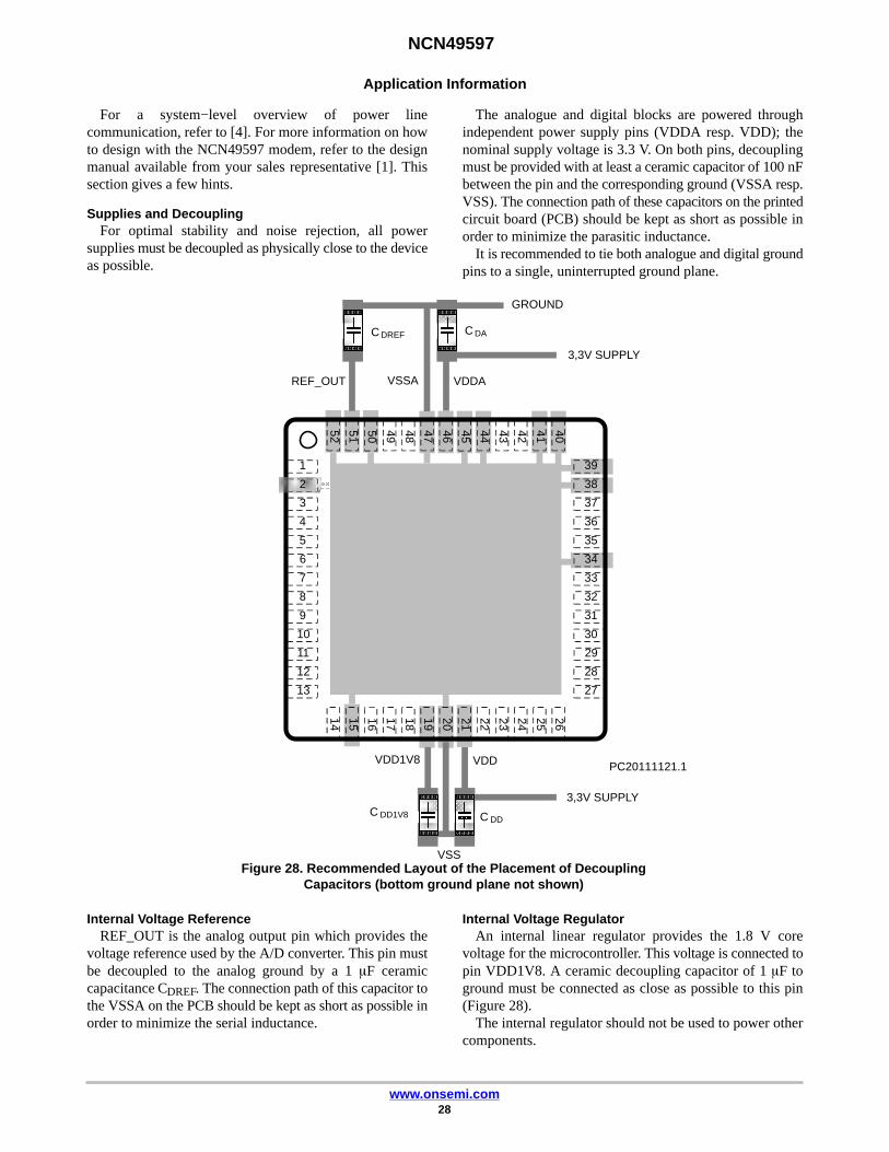
Supplies and DecouplingFor optimal stability and noise rejection, all power
supplies must be decoupled as physically close to the deviceas possible.
The analogue and digital blocks are powered throughindependent power supply pins (VDDA resp. VDD); thenominal supply voltage is 3.3 V. On both pins, decouplingmust be provided with at least a ceramic capacitor of 100 nFbetween the pin and the corresponding ground (VSSA resp.VSS). The connection path of these capacitors on the printedcircuit board (PCB) should be kept as short as possible inorder to minimize the parasitic inductance.
It is recommended to tie both analogue and digital groundpins to a single, uninterrupted ground plane.
Figure 28. Recommended Layout of the Placement of DecouplingCapacitors (bottom ground plane not shown)
PC20111121.1
1
3
4
5
6
7
8
9
10
11
12
13
26252423222120191817161514
39
38
37
36
35
34
33
32
31
30
29
28
27
40414243444546474849505152
REF_OUT VSSA VDDA
VDD1V8
VSS
VDD
C DD
C DAC DREF
GROUND
3,3V SUPPLY
3,3V SUPPLYC DD1V8
2
Internal Voltage ReferenceREF_OUT is the analog output pin which provides the
voltage reference used by the A/D converter. This pin mustbe decoupled to the analog ground by a 1 �F ceramiccapacitance CDREF. The connection path of this capacitor tothe VSSA on the PCB should be kept as short as possible inorder to minimize the serial inductance.
Internal Voltage RegulatorAn internal linear regulator provides the 1.8 V core
voltage for the microcontroller. This voltage is connected topin VDD1V8. A ceramic decoupling capacitor of 1 �F toground must be connected as close as possible to this pin(Figure 28).
The internal regulator should not be used to power othercomponents.
NCN49597
www.onsemi.com29
References
In this document references are made to:1. ON Semiconductor, Design Manual
NCN495979/9, 2016−08−23. The latest version isavailable from your sales representative.
2. CENELEC. EN 50065−1: Signaling on low−voltage electrical installations in the frequencyrange 3 kHz to 148,5 kHz. 2011−04−22. Online athttp://www.cenelec.eu/dyn/www/f?p=104:110:1022556227334229::::FSP_ORG_ID,FSP_PROJECT,FSP_LANG_ID:821,22484,25
3. ON Semiconductor. Mains synchronization forPLC modems (application note). 2015−08−19. Thelatest version is available from your salesrepresentative.
4. ON Semiconductor. AND9165/D. Getting startedwith power line communication (application note).2016−05−01. Online athttp://www.onsemi.com/pub_link/Collateral/AND9165−D.PDF
Table 14. ORDERING INFORMATION
Part Number Temperature Range Package Type Shipping†
NCN49597MNG −40°C – 125°C QFN−52(Pb−Free)
Tube
NCN49597MNRG −40°C – 125°C QFN−52(Pb−Free)
Tape & Reel
†For information on tape and reel specifications, including part orientation and tape sizes, please refer to our Tape and Reel PackagingSpecification Brochure, BRD8011/D.
NCN49597
www.onsemi.com30
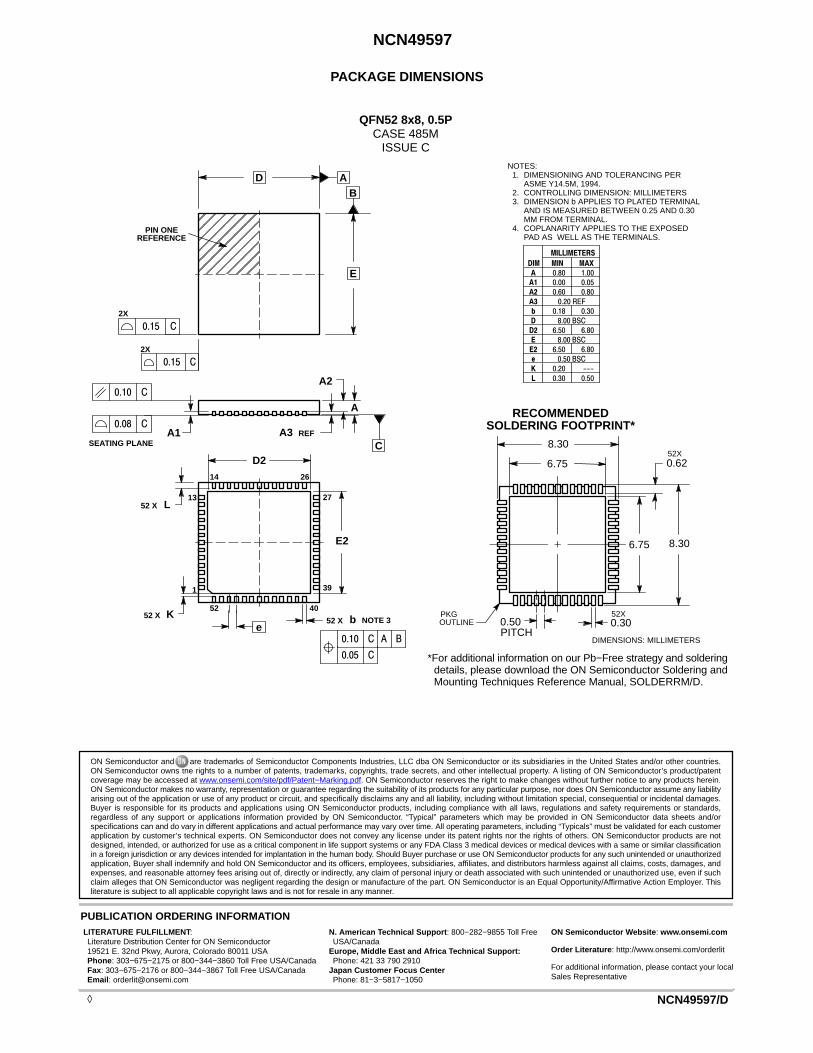
PACKAGE DIMENSIONS
ÉÉÉÉÉÉÉÉÉÉÉÉÉÉÉÉ
QFN52 8x8, 0.5PCASE 485M
ISSUE C
C0.15
NOTES:1. DIMENSIONING AND TOLERANCING PER
ASME Y14.5M, 1994.2. CONTROLLING DIMENSION: MILLIMETERS3. DIMENSION b APPLIES TO PLATED TERMINAL
AND IS MEASURED BETWEEN 0.25 AND 0.30MM FROM TERMINAL.
4. COPLANARITY APPLIES TO THE EXPOSEDPAD AS WELL AS THE TERMINALS.
AD
E
B
C0.08A1 A3
A
D2
L
NOTE 3
C0.15
2X
2X
SEATING PLANE
C0.10A2
C
E2
52 X
e
1
13
14 26
27
39
4052
b52 X
A0.10 BC
0.05 C
DIM MIN MAXMILLIMETERS
A 0.80 1.00A1 0.00 0.05A2 0.60 0.80A3 0.20 REFb 0.18 0.30D 8.00 BSCD2 6.50 6.80E 8.00 BSCE2 6.50 6.80e 0.50 BSCK 0.20 ---
REF
K52 X
L 0.30 0.50
PIN ONEREFERENCE
SOLDERING FOOTPRINT*
DIMENSIONS: MILLIMETERS
8.30
6.75
6.75
0.50
0.62
0.30
52X
52X
PITCH
8.30
PKGOUTLINE
RECOMMENDED
*For additional information on our Pb−Free strategy and solderingdetails, please download the ON Semiconductor Soldering andMounting Techniques Reference Manual, SOLDERRM/D.
ON Semiconductor and are trademarks of Semiconductor Components Industries, LLC dba ON Semiconductor or its subsidiaries in the United States and/or other countries.ON Semiconductor owns the rights to a number of patents, trademarks, copyrights, trade secrets, and other intellectual property. A listing of ON Semiconductor’s product/patentcoverage may be accessed at www.onsemi.com/site/pdf/Patent−Marking.pdf. ON Semiconductor reserves the right to make changes without further notice to any products herein.ON Semiconductor makes no warranty, representation or guarantee regarding the suitability of its products for any particular purpose, nor does ON Semiconductor assume any liabilityarising out of the application or use of any product or circuit, and specifically disclaims any and all liability, including without limitation special, consequential or incidental damages.Buyer is responsible for its products and applications using ON Semiconductor products, including compliance with all laws, regulations and safety requirements or standards,regardless of any support or applications information provided by ON Semiconductor. “Typical” parameters which may be provided in ON Semiconductor data sheets and/orspecifications can and do vary in different applications and actual performance may vary over time. All operating parameters, including “Typicals” must be validated for each customerapplication by customer’s technical experts. ON Semiconductor does not convey any license under its patent rights nor the rights of others. ON Semiconductor products are notdesigned, intended, or authorized for use as a critical component in life support systems or any FDA Class 3 medical devices or medical devices with a same or similar classificationin a foreign jurisdiction or any devices intended for implantation in the human body. Should Buyer purchase or use ON Semiconductor products for any such unintended or unauthorizedapplication, Buyer shall indemnify and hold ON Semiconductor and its officers, employees, subsidiaries, affiliates, and distributors harmless against all claims, costs, damages, andexpenses, and reasonable attorney fees arising out of, directly or indirectly, any claim of personal injury or death associated with such unintended or unauthorized use, even if suchclaim alleges that ON Semiconductor was negligent regarding the design or manufacture of the part. ON Semiconductor is an Equal Opportunity/Affirmative Action Employer. Thisliterature is subject to all applicable copyright laws and is not for resale in any manner.
PUBLICATION ORDERING INFORMATIONN. American Technical Support: 800−282−9855 Toll FreeUSA/Canada
Europe, Middle East and Africa Technical Support:Phone: 421 33 790 2910
Japan Customer Focus CenterPhone: 81−3−5817−1050
NCN49597/D
LITERATURE FULFILLMENT:Literature Distribution Center for ON Semiconductor19521 E. 32nd Pkwy, Aurora, Colorado 80011 USAPhone: 303−675−2175 or 800−344−3860 Toll Free USA/CanadaFax: 303−675−2176 or 800−344−3867 Toll Free USA/CanadaEmail: [email protected]
ON Semiconductor Website: www.onsemi.com
Order Literature: http://www.onsemi.com/orderlit
For additional information, please contact your localSales Representative
◊