UM10422 TDA5051A power line modem evaluation · PDF fileDocument information UM10422 TDA5051A...
15
UM10422 TDA5051A power line modem evaluation board Rev. 2 — 1 June 2011 User manual Document information Info Content Keywords Mains supply, TDA5051A, zero cross detector Abstract This document is a user manual for the TDA5051A power line modem stand-alone evaluation board.
Transcript of UM10422 TDA5051A power line modem evaluation · PDF fileDocument information UM10422 TDA5051A...

UM10422TDA5051A power line modem evaluation boardRev. 2 — 1 June 2011 User manual
Document information
Info Content
Keywords Mains supply, TDA5051A, zero cross detector
Abstract This document is a user manual for the TDA5051A power line modem stand-alone evaluation board.

NXP Semiconductors UM10422TDA5051A power line modem evaluation board
Revision history
Rev Date Description
v.3 20110601 user manual; third release
Added waveforms in Section 5
v.2 20110104 user manual; second release
Evaluation board, PCB layout, and BOM are updated to V2.
v.1 20101102 user manual; first release
UM10422 All information provided in this document is subject to legal disclaimers. © NXP B.V. 2011. All rights reserved.
User manual Rev. 2 — 1 June 2011 2 of 15
Contact informationFor more information, please visit: http://www.nxp.com
For sales office addresses, please send an email to: [email protected]

NXP Semiconductors UM10422TDA5051A power line modem evaluation board
1. Introduction
The TDA5051A is a Power Line Modem (PLM) IC, specifically dedicated to ASK transmission by means of home power line network at 600 baud or 1200 baud data rate. It operates from a single 5 V supply.
The TDA5051A employs control logic which provides full digital carrier generation and shaping, a high clock rate of 6-bit D/A (Digital-to-Analog) converter which provides rejection of aliasing components. The IC contains a fully integrated output power stage with overload protection. The receiver employs an AGC (Automatic Gain Control), 8-bit A/D (Analog-to-Digital) converter and narrowband digital baseband filtering and digital demodulator. The modulation and demodulation frequency is set by clock source from microcontroller or on-chip crystal oscillator.
Easy compliance with EN50065-1 is afforded with simple coupling networks. Low cost applications are realized with few external components. The TDA5051A is housed in the SO16 plastic package.
2. Safety warning
The board needs to be connected to mains voltage. Touching the reference board during operation must be avoided at all times. An isolated housing is obligatory when used in uncontrolled, non-laboratory environments. This isolation is not according to any regulated norm. Galvanic isolation of the mains phase using a variable transformer is always recommended. These devices can be recognized by the symbols shown in Figure 1.
WARNING
Lethal voltage and fire ignition hazard
The non-insulated high voltages that are present when operating this product, constitute a risk of electric shock, personal injury, death and/or ignition of fire.
This product is intended for evaluation purposes only. It shall be operated in a designated test area by personnel that is qualified according to local requirements and labor laws to work with non-insulated mains voltages and high-voltage circuits. This product shall never be operated unattended.
a. Isolated b. Not isolated
Fig 1. Variac isolation symbols
002aaf717 002aaf718
UM10422 All information provided in this document is subject to legal disclaimers. © NXP B.V. 2011. All rights reserved.
User manual Rev. 2 — 1 June 2011 3 of 15

NXP Semiconductors UM10422TDA5051A power line modem evaluation board
3. Specifications
Table 1 gives specifications for TDA5051A Power Line Modem (PLM) IC.
[1] The value of the total transmission mode current is the sum of IDD(RX/TX)(tot) + IDD(PAMP) in Table 5 “Characteristics” of the TDA5051A data sheet.
[2] Frequency range corresponding to the EN50065-1 band. However, the modem can operate at any lower oscillator frequency.
[3] The minimum value can be improved by using an external amplifier.
4. Evaluation board
Table 1. Quick reference data
Symbol Parameter Conditions Min Typ Max Unit
VDD supply voltage 4.75 5.0 5.25 V
IDD(tot) total supply current fosc = 8.48 MHz
Reception mode - 28 38 mA
Transmission mode; DATA_IN = 0; ZL = 30 Ω
[1] - 47 68 mA
Power-down mode - 19 25 mA
fcr carrier frequency [2] - 132.5 - kHz
fosc oscillator frequency 6.08 - 9.504 MHz
Vo(rms) output carrier signal (RMS value) DATA_IN = LOW; ZL = CISPR16 120 - 122 dBμV
Vi(rms) input signal (RMS value) [3] 82 - 122 dBμV
THD total harmonic distortion on CISPR16 load with coupling network
- −55 - dB
Tamb ambient temperature −10 - +80 °C
Fig 2. Evaluation board photo
019aaa515
UM10422 All information provided in this document is subject to legal disclaimers. © NXP B.V. 2011. All rights reserved.
User manual Rev. 2 — 1 June 2011 4 of 15

NXP Semiconductors UM10422TDA5051A power line modem evaluation board
5. Connecting the board
The PLM evaluation board can be used for a 230 A (AC) (50 Hz) or for a 120 V (AC) (60 Hz) mains power line. If a galvanic isolated power transformer is used, it should be placed between the AC power line and the PLM evaluation board.
Select a power line plug/cable depending on power line supply voltage and safety enclosure used in test bench setup.
Remark: When the board is placed in a metal enclosure, the middle pin of the power plug can be connected to the metal casing for grounding.
5.1 PLM test setup
Table 2. General setup
General setup
Connect Line to Line, and Neutral to Neutral.
Connect +5 V DC to pin 1.
Connect GND to pin 3 and pin 5.
Set pulse generator to square wave (0 V to 5 V), 1200 Hz, 50 % duty cycle.
Fig 3. PLM test setup (board to board)
019aaa514
PLM_I/F interface connectorpinning shown in Table 4
Power line inputs:JP1 (L) and JP2 (N) areconnected to AC power cord.
When probing the carrier signalat L and N inputs, these inputsmust be isolated with anisolation transformer.
UM10422 All information provided in this document is subject to legal disclaimers. © NXP B.V. 2011. All rights reserved.
User manual Rev. 2 — 1 June 2011 5 of 15

NXP Semiconductors UM10422TDA5051A power line modem evaluation board
[1] The average current (I) for each chip is approximately 30 mA to 40 mA.
[2] You will experience higher currents if you do not disable the Tx pin of the receiving device.
[3] You can also monitor the ASK signaling on the L and N pins (no line voltage applied).
CAUTION: You must use an isolated scope if you apply 110 V AC to the L and N inputs.
Table 3. Transmission test setup
Transmission test (A to B) Transmission test (B to A)
Connect pin 4 of board A to pulse generator
Connect pin 4 of board B to +5 V DC (disables Tx)
Connect a scope probe to pin 4 of board A
Connect a scope probe to pin 6 of board B
Connect pin 4 of board B to pulse generator
Connect pin 4 of board A to +5 V DC (disables Tx)
Connect scope probe to pin 4 of board B
Connect scope probe to pin 6 of board A
Table 4. PLM_I/F connector pin description
Pin Description
1 +5 V DC supply input
2 Oscillator 1
3 GND
4 DATA_IN; data input, active LOW
5 GND
6 DATA_OUT; data output, active LOW
7 zero cross detector
8 power down (active HIGH)
UM10422 All information provided in this document is subject to legal disclaimers. © NXP B.V. 2011. All rights reserved.
User manual Rev. 2 — 1 June 2011 6 of 15

NXP Semiconductors UM10422TDA5051A power line modem evaluation board
Fig 4. Printed-circuit board layout
019aaa516
UM10422 All information provided in this document is subject to legal disclaimers. © NXP B.V. 2011. All rights reserved.
User manual Rev. 2 — 1 June 2011 7 of 15
NXP Semiconductors UM10422TDA5051A power line modem evaluation board
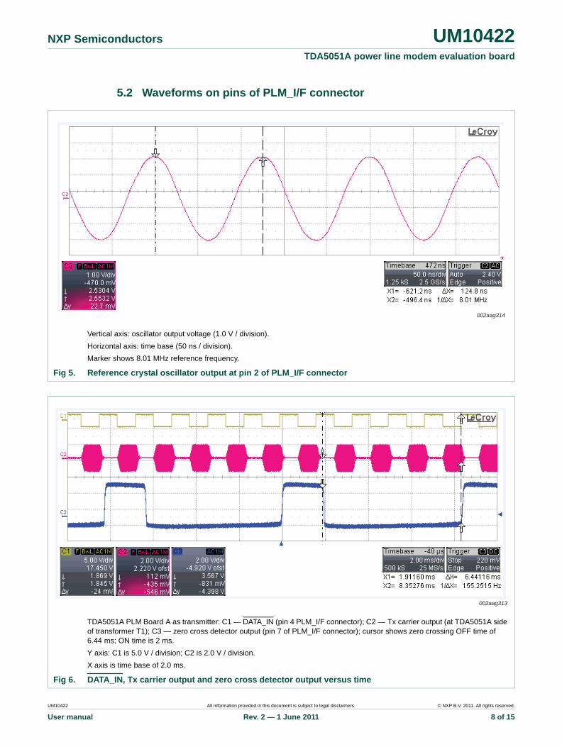
5.2 Waveforms on pins of PLM_I/F connector
Vertical axis: oscillator output voltage (1.0 V / division).
Horizontal axis: time base (50 ns / division).
Marker shows 8.01 MHz reference frequency.
Fig 5. Reference crystal oscillator output at pin 2 of PLM_I/F connector
002aag314
TDA5051A PLM Board A as transmitter: C1 — DATA_IN (pin 4 PLM_I/F connector); C2 — Tx carrier output (at TDA5051A side of transformer T1); C3 — zero cross detector output (pin 7 of PLM_I/F connector); cursor shows zero crossing OFF time of 6.44 ms; ON time is 2 ms.
Y axis: C1 is 5.0 V / division; C2 is 2.0 V / division.
X axis is time base of 2.0 ms.
Fig 6. DATA_IN, Tx carrier output and zero cross detector output versus time
002aag313
UM10422 All information provided in this document is subject to legal disclaimers. © NXP B.V. 2011. All rights reserved.
User manual Rev. 2 — 1 June 2011 8 of 15

NXP Semiconductors UM10422TDA5051A power line modem evaluation board
Board A as transmitter: C1 — DATA_IN (pin 4 of PLM_I/F connector); C2 — Tx carrier output (at TDA5051A side of transformer T1); cursor shows DATA_IN to Tx carrier output lead of 169.95 μs.
Y axis: C1 is 2.0 V / division; C2 is 2.0 V / division.
X axis is time base of 200 μs.
Fig 7. DATA_IN to Tx carrier output delay
002aag316
Board B as receiver: C1 — DATA_OUT (pin 6 of PLM_I/F connector); C2 — Rx carrier input (at TDA5051A side of transformer T1); cursor shows DATA_OUT to Rx carrier input delay of 132.3 μs.
Y axis: C1 is 2.0 V / division; C2 is 20 mV / division.
X axis is time base of 200 μs.
Fig 8. Rx carrier input to DATA_OUT delay
002aag315
UM10422 All information provided in this document is subject to legal disclaimers. © NXP B.V. 2011. All rights reserved.
User manual Rev. 2 — 1 June 2011 9 of 15

NXP Semiconductors UM10422TDA5051A power line modem evaluation board
6. Functional description
Refer to data sheet TDA5051A for functional description. www.nxp.com/pip/TDA5051A.html
Board B as receiver: C1 — DATA_OUT (pin 6 of PLM_I/F connector); C2 — Rx carrier input (at TDA5051A side of transformer T1); cursor shows zero cross detector peak-to-peak period of approximately 120 Hz.
Y axis: C1 is 2.0 V / division; C2 is 20 mV / division; C3 is 2.0 V / division.
X axis is time base of 2.0 μs.
Fig 9. Rx carrier input noise is greater at peaks of AC power line waveform
002aag317
UM10422 All information provided in this document is subject to legal disclaimers. © NXP B.V. 2011. All rights reserved.
User manual Rev. 2 — 1 June 2011 10 of 15

NXP Semiconductors UM10422TDA5051A power line modem evaluation board
7. Board schematic
Fig 10. PLM evaluation board schematic
002aaf722
VD
DD
VD
DA
PV
DD
A
31113D
GN
DA
PG
ND
AG
ND
5912
GND
SC
AN
TE
ST
6
OS
C2
8
OS
C1
7
R7
2.2 MΩ
X18 MHz
C127 pF
C227 pF
Install for crystal operation.NOTE: X1, R7, C1 and C3 optional.Carrier set to 125 kHz.
CLK_OUT
DATA_OUT
4
2
PD15
DATA_IN1
10
14
16
TX_OUT
RX_IN
TEST1
C60.1 μF
IC1TDA5051A
R1
100 Ω
C5
C3
10 μF, 16 V
0.1 μF, 25 V
L222 μH(RFB0807-220L)
D1PTVS7V0S1UR
GND
1 2 3456
T178250MC
L147 μH
(RFB0807-470L)
C947 nF
(MPXQS47K)
C4100 μF
C70.1 μF
C80.1 μF
+5 V
Q1PMBT3904
R510 kΩ
R4
1 kΩ
+5 V
zero cross detector
531
7642
8
PLM_I/F
PS
GND
65
4
OC1
IL250SM
R2
220 kΩ
1
2R31 MΩ
U
R6V250LA4P
F1370-0630-04101
1
AC 0 V to 220 V
JP1
JP2
DC 0 V to 48 V
WARNING:HIGH VOLTAGE
642
8531
7
PWM
PWM feed thru
642
8531
7
N/C
R84.7 kΩ
+5 V
C102200 pF
UM10422 All information provided in this document is subject to legal disclaimers. © NXP B.V. 2011. All rights reserved.
User manual Rev. 2 — 1 June 2011 11 of 15
NXP Semiconductors UM10422TDA5051A power line modem evaluation board
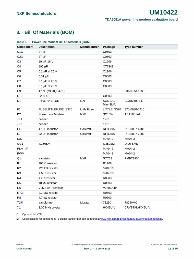
8. Bill Of Materials (BOM)
[1] Optional for XTAL.
[2] Specifications for component T1 signal transformer can be found at www.nxp.com/redirect/murata-ps.com/data/magnetics.
Table 5. Power line modem Bill Of Materials (BOM)
Component Description Manufacturer Package Type number
C1[1] 27 pF C0603
C2[1] 27 pF C0603
C3 10 μF, 16 V C1206
C4 100 μF CT7343
C5 0.1 μF at 25 V C1206
C6 0.01 μF C0603
C7 0.1 μF at 25 V C0603
C8 0.1 μF at 25 V C0603
C9 47 nF (MPXQS47K) C150-054X183
C10 2200 pF C0603
D1 PTVS7V0S1UR NXP SOD123, Mini-SMA
CGRM4001-G
F1 FUSELITTLEFUSE_S370 Little Fuse LITTLE_S370 370-0630-0410
IC1 Power Line Modem NXP SO16W TDA5051AT
JP1 header 1X01
JP2 header 1X01
L1 47 μH inductor Coilcraft RFB0807 RFB0807-470L
L2 22 μH inductor Coilcraft RFB0807 RFB0807-220L
N/C MA04-2 MA04-2
OC1 IL250SM IL250SM DIL6-SMD
PLM_I/F MA04-2 MA04-2
PWM MA04-2 MA04-2
Q1 transistor NXP SOT23 PMBT3904
R1 100 Ω resistor R1206
R2 220 kΩ resistor 0207/10
R3 1 MΩ resistor 0207/10
R4 1 kΩ resistor R0603
R5 10 kΩ resistor R0603
R6 V250LA4P resistor V250LA4P
R7[1] 2.2 MΩ resistor R0603
R8 4.7 kΩ resistor R0603
T1[2] transformer Murata 78250 78250MC
X1 8.00 MHz crystal HC49U-V CRYSTALHC49U-V
UM10422 All information provided in this document is subject to legal disclaimers. © NXP B.V. 2011. All rights reserved.
User manual Rev. 2 — 1 June 2011 12 of 15

NXP Semiconductors UM10422TDA5051A power line modem evaluation board
9. Abbreviations
Table 6. Abbreviations
Acronym Description
ADC Analog-to-Digital Converter
AGC Automatic Gain Control
ASK Amplitude Shift Keying
CMOS Complementary Metal-Oxide Semiconductor
DAC Digital-to-Analog Converter
HF High-Frequency
IC Integrated Circuit
LC inductor-capacitor filter
PLM Power Line Modem
RMS Root Mean Squared
TTL Transistor-Transistor Logic
UM10422 All information provided in this document is subject to legal disclaimers. © NXP B.V. 2011. All rights reserved.
User manual Rev. 2 — 1 June 2011 13 of 15

NXP Semiconductors UM10422TDA5051A power line modem evaluation board
10. Legal information
10.1 Definitions
Draft — The document is a draft version only. The content is still under internal review and subject to formal approval, which may result in modifications or additions. NXP Semiconductors does not give any representations or warranties as to the accuracy or completeness of information included herein and shall have no liability for the consequences of use of such information.
10.2 Disclaimers
Limited warranty and liability — Information in this document is believed to be accurate and reliable. However, NXP Semiconductors does not give any representations or warranties, expressed or implied, as to the accuracy or completeness of such information and shall have no liability for the consequences of use of such information.
In no event shall NXP Semiconductors be liable for any indirect, incidental, punitive, special or consequential damages (including - without limitation - lost profits, lost savings, business interruption, costs related to the removal or replacement of any products or rework charges) whether or not such damages are based on tort (including negligence), warranty, breach of contract or any other legal theory.
Notwithstanding any damages that customer might incur for any reason whatsoever, NXP Semiconductors’ aggregate and cumulative liability towards customer for the products described herein shall be limited in accordance with the Terms and conditions of commercial sale of NXP Semiconductors.
Right to make changes — NXP Semiconductors reserves the right to make changes to information published in this document, including without limitation specifications and product descriptions, at any time and without notice. This document supersedes and replaces all information supplied prior to the publication hereof.
Suitability for use — NXP Semiconductors products are not designed, authorized or warranted to be suitable for use in life support, life-critical or safety-critical systems or equipment, nor in applications where failure or malfunction of an NXP Semiconductors product can reasonably be expected to result in personal injury, death or severe property or environmental damage. NXP Semiconductors accepts no liability for inclusion and/or use of NXP Semiconductors products in such equipment or applications and therefore such inclusion and/or use is at the customer’s own risk.
Applications — Applications that are described herein for any of these products are for illustrative purposes only. NXP Semiconductors makes no representation or warranty that such applications will be suitable for the specified use without further testing or modification.
Customers are responsible for the design and operation of their applications and products using NXP Semiconductors products, and NXP Semiconductors accepts no liability for any assistance with applications or customer product
design. It is customer’s sole responsibility to determine whether the NXP Semiconductors product is suitable and fit for the customer’s applications and products planned, as well as for the planned application and use of customer’s third party customer(s). Customers should provide appropriate design and operating safeguards to minimize the risks associated with their applications and products.
NXP Semiconductors does not accept any liability related to any default, damage, costs or problem which is based on any weakness or default in the customer’s applications or products, or the application or use by customer’s third party customer(s). Customer is responsible for doing all necessary testing for the customer’s applications and products using NXP Semiconductors products in order to avoid a default of the applications and the products or of the application or use by customer’s third party customer(s). NXP does not accept any liability in this respect.
Export control — This document as well as the item(s) described herein may be subject to export control regulations. Export might require a prior authorization from national authorities.
Evaluation products — This product is provided on an “as is” and “with all faults” basis for evaluation purposes only. NXP Semiconductors, its affiliates and their suppliers expressly disclaim all warranties, whether express, implied or statutory, including but not limited to the implied warranties of non-infringement, merchantability and fitness for a particular purpose. The entire risk as to the quality, or arising out of the use or performance, of this product remains with customer.
In no event shall NXP Semiconductors, its affiliates or their suppliers be liable to customer for any special, indirect, consequential, punitive or incidental damages (including without limitation damages for loss of business, business interruption, loss of use, loss of data or information, and the like) arising out the use of or inability to use the product, whether or not based on tort (including negligence), strict liability, breach of contract, breach of warranty or any other theory, even if advised of the possibility of such damages.
Notwithstanding any damages that customer might incur for any reason whatsoever (including without limitation, all damages referenced above and all direct or general damages), the entire liability of NXP Semiconductors, its affiliates and their suppliers and customer’s exclusive remedy for all of the foregoing shall be limited to actual damages incurred by customer based on reasonable reliance up to the greater of the amount actually paid by customer for the product or five dollars (US$5.00). The foregoing limitations, exclusions and disclaimers shall apply to the maximum extent permitted by applicable law, even if any remedy fails of its essential purpose.
10.3 TrademarksNotice: All referenced brands, product names, service names and trademarks are the property of their respective owners.
UM10422 All information provided in this document is subject to legal disclaimers. © NXP B.V. 2011. All rights reserved.
User manual Rev. 2 — 1 June 2011 14 of 15

NXP Semiconductors UM10422TDA5051A power line modem evaluation board
11. Contents
1 Introduction . . . . . . . . . . . . . . . . . . . . . . . . . . . . 3
2 Safety warning . . . . . . . . . . . . . . . . . . . . . . . . . . 3
3 Specifications. . . . . . . . . . . . . . . . . . . . . . . . . . . 4
4 Evaluation board . . . . . . . . . . . . . . . . . . . . . . . . 4
5 Connecting the board . . . . . . . . . . . . . . . . . . . . 55.1 PLM test setup . . . . . . . . . . . . . . . . . . . . . . . . . 55.2 Waveforms on pins of PLM_I/F connector . . . . 8
6 Functional description . . . . . . . . . . . . . . . . . . 10
7 Board schematic . . . . . . . . . . . . . . . . . . . . . . . 11
8 Bill Of Materials (BOM) . . . . . . . . . . . . . . . . . . 12
9 Abbreviations. . . . . . . . . . . . . . . . . . . . . . . . . . 13
10 Legal information. . . . . . . . . . . . . . . . . . . . . . . 1410.1 Definitions. . . . . . . . . . . . . . . . . . . . . . . . . . . . 1410.2 Disclaimers . . . . . . . . . . . . . . . . . . . . . . . . . . . 1410.3 Trademarks. . . . . . . . . . . . . . . . . . . . . . . . . . . 14
11 Contents . . . . . . . . . . . . . . . . . . . . . . . . . . . . . . 15
© NXP B.V. 2011. All rights reserved.
For more information, please visit: http://www.nxp.comFor sales office addresses, please send an email to: [email protected]
Date of release: 1 June 2011
Document identifier: UM10422
Please be aware that important notices concerning this document and the product(s)described herein, have been included in section ‘Legal information’.