NAVAL POSTGRADUATE SCHOOL this research we have shown that for all three cases (FIR filter,...
79
NAVAL POSTGRADUATE SCHOOL MONTEREY, CALIFORNIA THESIS Approved for public release; distribution is unlimited EFFICIENT IMPLEMENTATION OF FILTERING AND RESAMPLING OPERATIONS ON FIELD PROGRAMMABLE GATE ARRAYS (FPGAs) FOR SOFTWARE DEFINED RADIO (SDR) by Georgios Giannoulis December 2008 Thesis Advisor: Roberto Cristi Thesis Co-advisor: Craig W. Rasmussen
-
Upload
truongxuyen -
Category
Documents
-
view
212 -
download
0
Transcript of NAVAL POSTGRADUATE SCHOOL this research we have shown that for all three cases (FIR filter,...

NAVAL
POSTGRADUATE SCHOOL
MONTEREY, CALIFORNIA
THESIS
Approved for public release; distribution is unlimited
EFFICIENT IMPLEMENTATION OF FILTERING AND RESAMPLING OPERATIONS ON FIELD
PROGRAMMABLE GATE ARRAYS (FPGAs) FOR SOFTWARE DEFINED RADIO (SDR)
by
Georgios Giannoulis
December 2008
Thesis Advisor: Roberto Cristi Thesis Co-advisor: Craig W. Rasmussen

THIS PAGE INTENTIONALLY LEFT BLANK

i
REPORT DOCUMENTATION PAGE Form Approved OMB No. 0704-0188 Public reporting burden for this collection of information is estimated to average 1 hour per response, including the time for reviewing instruction, searching existing data sources, gathering and maintaining the data needed, and completing and reviewing the collection of information. Send comments regarding this burden estimate or any other aspect of this collection of information, including suggestions for reducing this burden, to Washington headquarters Services, Directorate for Information Operations and Reports, 1215 Jefferson Davis Highway, Suite 1204, Arlington, VA 22202-4302, and to the Office of Management and Budget, Paperwork Reduction Project (0704-0188) Washington DC 20503. 1. AGENCY USE ONLY (Leave blank)
2. REPORT DATE December 2008
3. REPORT TYPE AND DATES COVERED Master’s Thesis
4. TITLE AND SUBTITLE Efficient Implementation of Filtering and Resampling Operations on Field Programmable Gate Arrays (FPGAs) for Software Defined Radio (SDR). 6. AUTHOR(S) Georgios Giannoulis
5. FUNDING NUMBERS
7. PERFORMING ORGANIZATION NAME(S) AND ADDRESS(ES) Naval Postgraduate School Monterey, CA 93943-5000
8. PERFORMING ORGANIZATION REPORT NUMBER
9. SPONSORING /MONITORING AGENCY NAME(S) AND ADDRESS(ES) N/A
10. SPONSORING/MONITORING AGENCY REPORT NUMBER
11. SUPPLEMENTARY NOTES The views expressed in this thesis are those of the author and do not reflect the official policy or position of the Department of Defense or the U.S. Government. 12a. DISTRIBUTION / AVAILABILITY STATEMENT Approved for public release; distribution is unlimited
12b. DISTRIBUTION CODE
13. ABSTRACT (maximum 200 words) In Software Defined Radios a good portion (or even the entirety) of the modulation and demodulation
processes is performed in the digital domain. The data rate of the transmitted information is very important, since efficiency is a key requirement in real time implementations and cost increases considerably with the number of samples per second to be processed. In this thesis, we address the problem of efficient design of the resampling operations, so that they can be implemented on Field Programmable Gate Arrays (FPGAs).
A set of filtering and resampling operations is developed in the Simulink environment through Xilinx/Simulink blocksets, where all the included subsystems of the design are fully accessible by the designer in any stage of operation. The key ingredient is the use of a Multiplier and Accumulator (MAC) architecture, which can be either time multiplexed for maximum hardware efficiency, or run on a parallel structure for maximum time efficiency.
15. NUMBER OF PAGES
79
14. SUBJECT TERMS Digital Signal Processing, Software Defined Radio, Field Programmable Gate Array, Resampling, Filtering, Xilinx, System Generator.
16. PRICE CODE
17. SECURITY CLASSIFICATION OF REPORT
Unclassified
18. SECURITY CLASSIFICATION OF THIS PAGE
Unclassified
19. SECURITY CLASSIFICATION OF ABSTRACT
Unclassified
20. LIMITATION OF ABSTRACT
UU NSN 7540-01-280-5500 Standard Form 298 (Rev. 8-98) Prescribed by ANSI Std. Z39.18

ii
THIS PAGE INTENTIONALLY LEFT BLANK
iii
Approved for public release; distribution is unlimited
EFFICIENT IMPLEMENTATION OF FILTERING AND RESAMPLING OPERATIONS ON FIELD PROGRAMMABLE GATE ARRAYS (FPGAs) FOR
SOFTWARE DEFINED RADIO (SDR)
Georgios Giannoulis Lieutenant, Hellenic Navy
B.S., Hellenic Naval Academy, 1997
Submitted in partial fulfillment of the requirements for the degrees of
MASTER OF SCIENCE IN ELECTRICAL ENGINEERING and
MASTER OF SCIENCE IN APPLIED MATHEMATICS
from the
NAVAL POSTGRADUATE SCHOOL December 2008
Author: Georgios Giannoulis
Approved by: Roberto Cristi Thesis Advisor
Craig W. Rasmussen Thesis Co-Advisor
Jeffrey Knorr Chairman, Department of Electrical and Computer Engineering
Carlos F. Borges Chairman, Department of Applied Mathematics

iv
THIS PAGE INTENTIONALLY LEFT BLANK

v
ABSTRACT
In Software Defined Radios a good portion (or even the entirety) of the
modulation and demodulation processes is performed in the digital domain. The data rate
of the transmitted information is very important, since efficiency is a key requirement in
real time implementations and cost increases considerably with the number of samples
per second to be processed. In this thesis, we address the problem of efficient design of
the resampling operations, so that they can be implemented on Field Programmable Gate
Arrays (FPGAs).
A set of filtering and resampling operations is developed in the Simulink
environment through Xilinx/Simulink blocksets, where all the included subsystems of the
design are fully accessible by the designer in any stage of operation. The key ingredient is
the use of a Multiplier and Accumulator (MAC) architecture, which can be either time
multiplexed for maximum hardware efficiency, or run on a parallel structure for
maximum time efficiency.

vi
THIS PAGE INTENTIONALLY LEFT BLANK
vii
TABLE OF CONTENTS
I. INTRODUCTION........................................................................................................1 A. BACKROUND .................................................................................................1
1. FPGA for Digital Signal Processing ...................................................1 2. Design Enviroment...............................................................................3
B. OBJECTIVE ....................................................................................................4 1. Efficient Use of the Dual Port Ram and DSP48 Xilinx Blocks ........5
C. RELATED WORK ..........................................................................................8
II. FINITE IMPULSE RESPONSE FILTER WITH ONE MAC (MULTIPLIER ACCUMULATOR)......................................................................................................9 A. THEORETICAL PERSPECTIVE.................................................................9 B. SOFTWARE IMPLEMENTATION ...........................................................10
1. Control Logic for Data and Filter Coefficients ...............................11 2. Alignment of Data and Filter Coefficients in the Dual Port
Ram .....................................................................................................14 3. Sequential Multiplication and Accumulation (MAC) of Data
and Filter Coefficients using DSP48.................................................15 C. RESULTS .......................................................................................................17
III. DECIMATION BY AN INTEGER FACTOR........................................................21 A. THEORETICAL PERSPECTIVE...............................................................21
1 Sampling Continuous Time Signals .................................................21 2. Analysis of Downsampling (Decimation) .........................................22 3. Efficient Implementation of Decimation Operation using Noble
Identities and Filter’s Polyphase Decomposition............................25 B. DECIMATION BY TWO WITH FIR MAC AND POLYPHASE
DECOMPOSITION.......................................................................................26 1. Software Implementation..................................................................27
a. Control Logic for Data and Filter Coefficients .....................29 b. Sequential Multiplication and Accumulation (MAC) of
Data and Filter Coefficients using the DSP48 ......................32 c. Results......................................................................................34
C. DECIMATION BY AN INTEGER FACTOR ‘D’ WITH FIR MAC AND POLYPHASE DECOMPOSITION....................................................36
IV. INTERPOLATION BY AN INTEGER FACTOR.................................................41 A. THEORETICAL PERSPECTIVE...............................................................41
1. Analysis of Upsampling (Interpolation)...........................................41 2. Efficient Implementation of Interpolation Operation using
Noble Identities and Filter’s Polyphase Decomposition.................43 B. INTERPOLATION BY TWO WITH FIR MAC AND POLYPHASE
DECOMPOSITION.......................................................................................45 1. Software Implementation..................................................................45
a. Control Logic for Data and Filter Coefficients .....................47

viii
b. Sequential Multiplication and Accumulation (MAC) of Data and Filter Coefficients using DSP48.............................50
c. Results......................................................................................52 C. INTERPOLATION BY AN INTEGER FACTOR ‘D’ WITH FIR
MAC AND POLYPHASE DECOMPOSITION.........................................53
V. CONCLUSIONS ........................................................................................................59 A. SUMMARY OF THE WORK ......................................................................59 B. SUGGESTION FOR FUTURE WORK ......................................................60
LIST OF REFERENCES......................................................................................................61
INITIAL DISTRIBUTION LIST .........................................................................................63
ix
LIST OF FIGURES
Figure 1. Actual view of FPGA VIRTEX 4 (From: [4])...................................................2 Figure 2. Physical view of FPGA VIRTEX-4 (From: [2])................................................2 Figure 3. Simulink environment using Xilinx...................................................................3 Figure 4. Basic Structure of Simulation. ...........................................................................4 Figure 5. Dual Port Ram Xilinx Block..............................................................................5 Figure 6. DSP48 Slice (From: [6]). ...................................................................................7 Figure 7. DSP48 Xilinx Block. .........................................................................................7 Figure 8. Discrete Convolution. ........................................................................................9 Figure 9. Finite Impulse Response Filter with One MAC. .............................................11 Figure 10. Controller. ........................................................................................................13 Figure 11. Time Representation of Simulation. ................................................................14 Figure 12. Outcome of Dual Port Ram..............................................................................15 Figure 13. Outcome of DSP48. .........................................................................................16 Figure 14. Frequency Spectrum of the Original and Filtered Signal (Sinusoidal Case). ..18 Figure 15. Frequency Spectrum of the Original and Filtered Signal (Gaussian White
Noise Case). .....................................................................................................19 Figure 16. Sampling Continuous Time Signals.................................................................22 Figure 17. Downsampling Operation. ...............................................................................23 Figure 18. Aliasing Effect in Frequency Spectrum...........................................................24 Figure 19. Filtering and Downsampling a Discrete Signal. ..............................................25 Figure 20. Efficient Implementation of Decimation. ........................................................26 Figure 21. Downsampling by Two....................................................................................28 Figure 22. Controller. ........................................................................................................30 Figure 23. Time Representation of Simulation. ................................................................31 Figure 24. Outcome of Dual Port Ram..............................................................................32 Figure 25. Outcome of DSP48. .........................................................................................33 Figure 26. Frequency Spectrum of the Original and Downsampled by Two Signal
without Aliasing Effect. ...................................................................................35 Figure 27. Frequency Spectrum of the Original and Downsampled by Two Signal
with Aliasing Effect. ........................................................................................36 Figure 28. Timing Diagram for Decimation by D.............................................................38 Figure 29. Frequency Spectrum of the Original and Downsampled by 4D = Signal. ....40 Figure 30. Upsampling Operation. ....................................................................................41 Figure 31. ‘Ghost’ Frequencies in Interpolation Operation. .............................................42 Figure 32. Upsampling and Filtering with LPF. ...............................................................43 Figure 33. Efficient Implementation of Interpolation. ......................................................44 Figure 34. Upsampling by Two.........................................................................................46 Figure 35. Controller. ........................................................................................................48 Figure 36. Time Representation of Simulation. ................................................................49 Figure 37. Outcome of Dual Port Ram..............................................................................50 Figure 38. Outcome of DSP48. .........................................................................................51 Figure 39. Frequency Spectrum of the Original and Upsampled by Two Signal. ............53

x
Figure 40. Timing Diagram for Interpolation by D...........................................................55 Figure 41. Frequency Spectrum of the Original and Upsampled by 4D = Signal. .........57

xi
EXECUTIVE SUMMARY
In Software Defined Radios (SDR) a good portion (or even the entirety) of the
modulation and demodulation process is performed in the digital domain. The
reconfigurability and the versatility of the SDR can be efficiently supported by the Field
Programmable Gate Arrays (FPGAs) for hardware implementations.
FPGAs are high performance integrated circuits suitable for many Digital Signal
Processing (DSP) applications with the feature of being reprogrammable by the designer.
In this way, the system can be easily reconfigured to a number of different applications.
The proper software needed to program an FPGA is provided by System
Generator (Sysgen), which is an FPGA design program responsible for driving the FPGA
through the high-level design environment of Simulink. A combination of common and
synthesized Simulink/Xilinx blocks from the Simulink library along with MATLAB
codes have been used in order to construct a configurable scheme capable of
implementing the following three operations:
a) Finite Impulse Response (FIR) filter
b) Decimation by an integer factor
c) Interpolation by an integer factor
The key ingredient is the use of the Multiplier and Accumulator (MAC)
architecture, which can be either time multiplexed for maximum hardware efficiency, or
embedded on a parallel structure for maximum time efficiency.
The main components of the implementation are the Dual Port Ram Xilinx block,
which is a random access memory containing both data and the FIR filter coefficients,
together with the DSP48 Xilinx block, which performs the multiplication and addition on
a sequential basis. The DSP48 block is specifically designed for high-speed arithmetic
operations and it is part of the standard Xilinx Virtex family architecture. The objective is
to perform the proper arrangement of the input data and FIR filter coefficients so that the
resulting multiplication and accumulation will perform the three examined operations

xii
according to the theoretical formulations. Since the operations are performed serially, the
data need to be upsampled in order to handle the increased clock rate provided by System
Generator (Sysgen) and then properly downsampled.
In this research we have shown that for all three cases (FIR filter, Decimation,
Interpolation) the overall structure is the same. What defines each operation is the control
logic (Controller) and the storing of the filter parameters.
The controller consists of logic blocks from the Xilinx blockset and it is
responsible for updating the Dual Port Ram’s memory vectors (according to Sysgen clock
rate) in order to provide the proper dual sequential output. The dual output of the memory
block is multiplied and accumulated by DSP48 math slice. The outcome of the DSP48 is
a bitstream in which the desired coefficient of the three examined operations are
embedded accordingly in multiple of the Sysgen rate. Therefore, the final output can be
obtained by downsampling the output of DSP48 with the proper factor.
MATLAB was used to verify the consistency of the simulation with the theory.

xiii
ACKNOWLEDGMENTS
Θα ήθελα να ευχαριστήσω και να εκφράσω την βαθιά μου αγάπη στη σύζυγο μου
Ελένη και στα παιδιά μου Δημοσθένη και Παναγιώτη που μου συμπαραστάθηκαν
καθ’όλη τη διάρκεια των σπουδών και της προσπάθειας ολοκλήρωσης της πτυχιακής,
επιδεικνύοντας ιδιαίτερη υπομονή και κατανόηση.
Ringrazio il mio insegnante e relatore Professor Roberto Cristi per la sua
disponibilità e il suo sostegno nella preparazione della mia tesi.
I would also like to thank my co-advisor Professor Craig W. Rasmussen for his
contribution to accomplish my thesis and the mathematical knowledge he imparted to me.

xiv
THIS PAGE INTENTIONALLY LEFT BLANK

1
I. INTRODUCTION
A. BACKROUND
In Software Defined Radio, the modulation and demodulation processes are
performed in the digital domain. The data rate of the transmitted signal is usually several
orders of magnitudes smaller than the data rate necessary to drive the Digital to Analog
Converters (DACs) at the radio frequency (RF). In real time implementations, since the
cost increases according to the number of samples per second, we need to adapt the
sampling rate to the frequency content of the transmitted signal. Therefore, signals at
radio frequency (RF) are sampled at a rate comparable to the RF frequency, while the
signals at baseband are sampled at the information rate [1]. The reconfigurability and the
versatility of the SDR can be efficiently supported by the Field Programmable Gate
Arrays (FPGAs) for hardware implementations.
1. FPGA for Digital Signal Processing
The Field Programmable Gate Array (FPGA) is a high performance integrated
circuit suitable for Digital Signal Processing (DSP) applications. An FPGA has the
feature of being programmable by the designer and it can be easily reprogrammed.
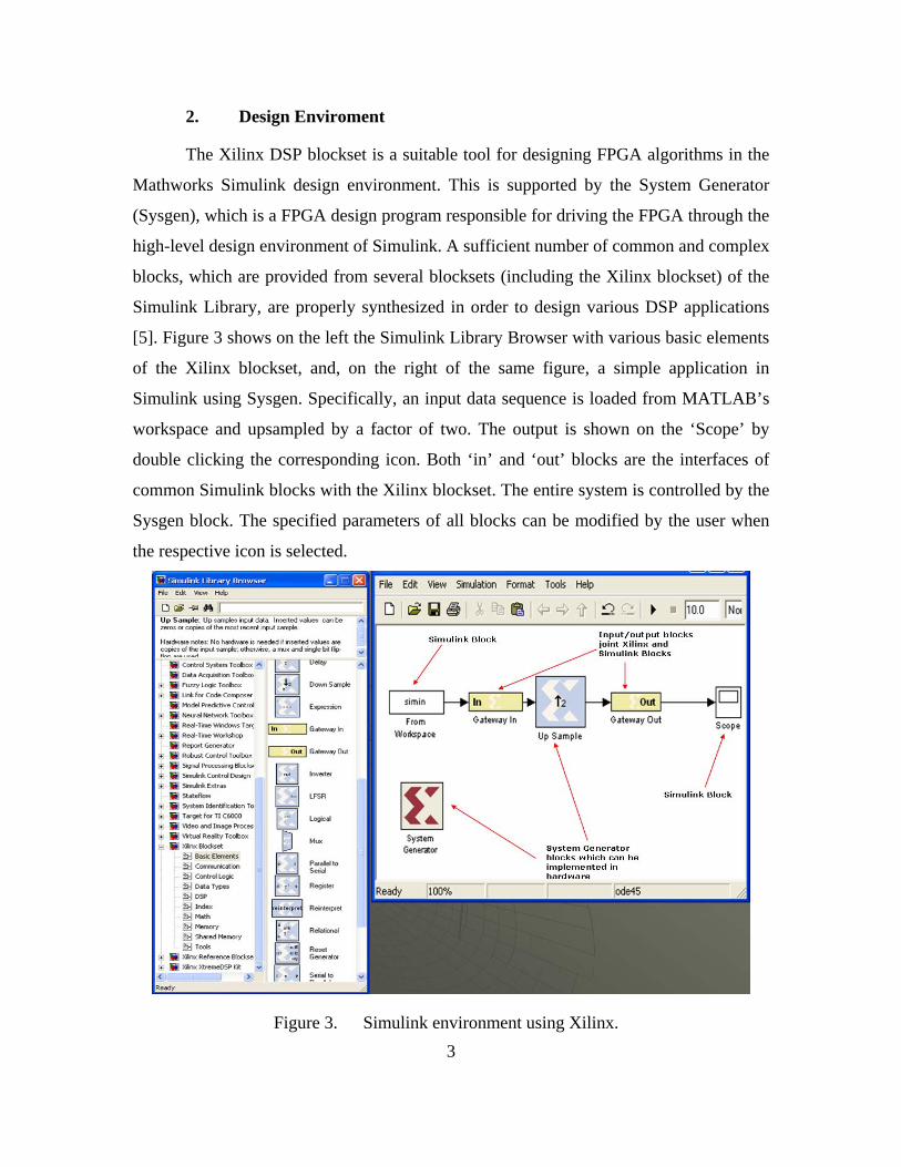
Physically, an FPGA is a two-dimensional array of gates consisting of various logic DSP
blocks and interconnections between them in order to perform DSP operations [2].
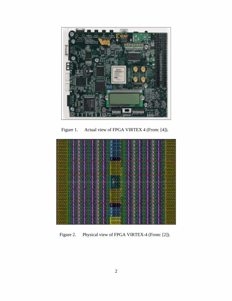
Figure 1 shows a Virtex-4 FPGA embedded in a processing board. Figure 2 shows
a number of important features such as the array of ‘slices’ disposed in columns of
macroblocks. The latter are blocks, constituted of memory and arithmetic units that are
programmed to perform suitable operations. The entire interconnected mesh can be
programmed into highly parallel algorithms [2].
2
Figure 1. Actual view of FPGA VIRTEX 4 (From: [4]).
Figure 2. Physical view of FPGA VIRTEX-4 (From: [2]).
3
2. Design Enviroment
The Xilinx DSP blockset is a suitable tool for designing FPGA algorithms in the
Mathworks Simulink design environment. This is supported by the System Generator
(Sysgen), which is a FPGA design program responsible for driving the FPGA through the
high-level design environment of Simulink. A sufficient number of common and complex
blocks, which are provided from several blocksets (including the Xilinx blockset) of the
Simulink Library, are properly synthesized in order to design various DSP applications
[5]. Figure 3 shows on the left the Simulink Library Browser with various basic elements
of the Xilinx blockset, and, on the right of the same figure, a simple application in
Simulink using Sysgen. Specifically, an input data sequence is loaded from MATLAB’s
workspace and upsampled by a factor of two. The output is shown on the ‘Scope’ by
double clicking the corresponding icon. Both ‘in’ and ‘out’ blocks are the interfaces of
common Simulink blocks with the Xilinx blockset. The entire system is controlled by the
Sysgen block. The specified parameters of all blocks can be modified by the user when
the respective icon is selected.
Figure 3. Simulink environment using Xilinx.

4
B. OBJECTIVE
In this thesis, we address the problem of efficient design of resampling operations
so they can be implemented on Field Programmable Gate Arrays (FPGAs). The key
ingredient is the use of a Multiplier and Accumulator (MAC) architecture, which will
allow us to perform the following operations:
1) Finite Impulse Response (FIR) filters
2) Decimation by an integer factor
3) Interpolation by an integer factor
The outcome of these three schemes is the development of a set of filtering and
resampling operations performed in Xilinx/Simulink. All the subsystems in the designs
are fully accessible by the designer.
In order to perform the three operations (FIR filtering, Decimation and
Interpolation by an integer factor), a basic design scheme in the Simulink environment is
used and is modified accordingly to fit the three cases. Since the objective is to develop
software suitable to programming FPGAs, a combination of Xilinx and Simulink blocks
as well as MATLAB codes is used. Figure 4 illustrates the basic structure of the
Simulation.
Figure 4. Basic Structure of Simulation.

5
In each of the three designs, the proper arrangement of the input data points and
Finite Impulse Response (FIR) filter coefficients is achieved in the Dual Port Ram Xilinx
block, which is a random access memory. The dual output of the memory block is
multiplied and accumulated by the DSP48 Xilinx block, which is an efficient block for
DSP operations implementing a Multiplier and Accumulator (MAC) operation. From the
resulting output, we selectively extract the data points of interest according to the
theoretical formulas of the three desired operations. Although several Xilinx/Simulink
blocks are used and are explained in the next chapters, the principal blocks are the Dual
Port Ram and the DSP48.
1. Efficient Use of the Dual Port Ram and DSP48 Xilinx Blocks
The Dual Port Ram Xilinx block is a dual memory device that allows the user to
specify the width and the values of each memory part. This specific block uses two sets
of ports dedicated to reading and writing of data. Each port has three inputs: (a) the
address line ‘addr’, (b) the input data ‘din’ and (c) the write enable ‘we’. In addition, each
port has one output. There is also an option of additional enable and synchronous reset
inputs for both ports that were not necessary for the purpose of this design. The Dual Port
Ram Xilinx block, along with its specified parameter window, is shown in Figure 5.
Figure 5. Dual Port Ram Xilinx Block.

6
Both memories are accessible for reading and writing by providing the right
address from the address ports ‘addra’ and ’addrb’. The initial value vector, as it is
indicated in the parameter window of Figure 5, is the concatenation of the two initial
vectors (initial data vector 0x and initial FIR filter coefficients h ). The ‘wea’ and ‘web’
are the write enable ports for each memory feeding the Dual Port Ram with a Boolean
signal ‘0’ or ‘1’.When the ‘we’ port is set to 1 then the memory writes the value of the
‘din’ port to the location specified by the corresponding address line. Each of the two
outputs depend on the write mode, which in our case is ‘read after write’, and it takes
exactly the same value indicted by the address line when the write cycle is completed [5].
For the purposes of this thesis, the second part of the memory remains unchanged
(no input data) and keeps the initial value. Specifically, input b takes the values of
properly ordered (according to the case of interest) finite impulse response (FIR) filter
coefficients, which are generated in the initialization of the simulation through any
MATLAB function such as ‘firpm’. Therefore ports ‘dinb’ and ‘web’ are fed with a
signed and a boolean zero respectively. On the other hand, the first part of the memory
changes according to ‘address’ and ‘write enable’ ports.
The outputs of ports A and B are two signed bit streams: one for the input data
points and one for coefficients of the FIR filter, aligned in such a way so that their
multiplication and accumulation will provide us the desired result for the three examined
cases.
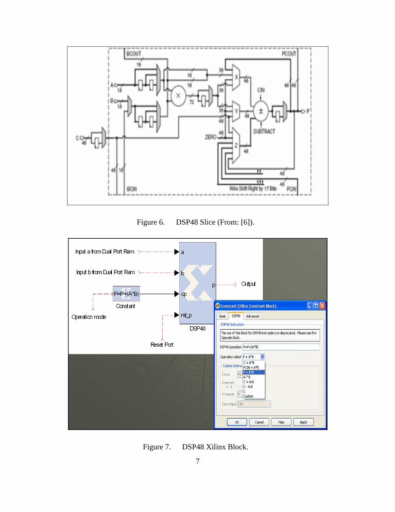
The DSP48 Xilinx block (also referred as an extreme DSP slice or DSP48 math
slice) is an efficient tool for many DSP applications, which can handle dynamically many
operations as well as be cascaded with other DSP48 blocks. It consists of an 18-bit-by-
18-bit signed multiplier with a 48-bit adder and a programmable multiplexer that can be
driven as required to perform specific operations [3]. The logic circuit of the slice is
depicted in Figure 6, while the corresponding Xilinx block along with some capable
operations is shown in Figure 7.
7
Figure 6. DSP48 Slice (From: [6]).
Figure 7. DSP48 Xilinx Block.

8
In this thesis the DSP48 is used as a multiplier and accumulator (MAC) block and
its operation is defined as P P A B= + ⋅ . With this block the product of two inputs A and
B (derived from the Dual Port Ram) is accumulated each time with the previous product
P . A reset port is available to the slice in order to reset the output every clock cycle to
produce the desired for each examined case operation.
C. RELATED WORK
Although a number of approaches to FIR filtering and resampling operations
design exist in literature ([10], [11]), to the best knowledge of the author there has been
no systematic way of designing these filters in a general fashion.
The main contribution of this resurch is an architecture, which is fully scalable to
any implementation in terms of filter coefficients and resampling factor.

9
II. FINITE IMPULSE RESPONSE FILTER WITH ONE MAC (MULTIPLIER ACCUMULATOR)
A. THEORETICAL PERSPECTIVE
In the digital domain, the output sequence [ ]y n of a Finite Impulse Response
(FIR) filter is given by the following expression:
[ ] [ ] [ ]0
N
ky n h k x n k
=
= ⋅ −∑ , (2.1)
where [ ]h n is the impulse response of the filter, [ ]x n is the input sequence and N being the degree of the transfer function of the FIR filter.
Both [ ]x n and [ ]y n are at the same clock rate x y sF F F= = as [ ] ( )sx n x nT= and
[ ] ( )sy n y nT= , where 1s
s
TF
= is the sampling interval [7]. The discrete convolution,
along with its graphical representation, is depicted in Figure 8.
Figure 8. Discrete Convolution.

10
We can verify from Figure 8 that the convolution operation can be graphically
implemented as a sliding window over a data sequence. In particular, at any time n we
need to save 1N + data points [ ] [ ] [ ], 1 ,...,x n x n x n N− − together with the
coefficients [ ] [ ] [ ]0 , 1 ,...,h h h N .
In this chapter, we address the problem of implementing the filtering operation
using one Multiplier and Accumulator (MAC). In this way, the convolution sum is
computed in about N clock pulses (where N denotes the degree of the transfer function
of the FIR filter), thus requiring a higher clock rate to be provided by the System
Generator, which controls the operation and its parameters. The objective is to perform
the proper arrangement of the input data points and the filter’s coefficients so that the
multiplication and accumulation procedure as well as the selective extraction of outcomes
will give us the desired convolution result in the most efficient way.
B. SOFTWARE IMPLEMENTATION
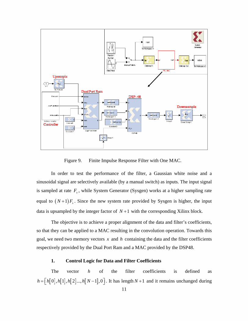
The Simulink/Xilinx implementation needed to perform the FIR filtering is shown
in Figure 9. The main components of the implementation are the Dual Port Ram, which
contains both data and the FIR filter coefficients and the DSP48, which performs the
multiplication and addition on a sequential basis. Since the operations are performed
serially, the data need to be upsampled in order to handle the increase of the clock rate
provided by System Generator. The controller consists of a set of counters (one for the
coefficients and one for the data points) along with logic blocks (implemented in Xilinx
blockset), and controls the flow of the data at the output of the dual Port Ram as well as
the timing of the operations.
11
Figure 9. Finite Impulse Response Filter with One MAC.
In order to test the performance of the filter, a Gaussian white noise and a
sinusoidal signal are selectively available (by a manual switch) as inputs. The input signal
is sampled at rate sF , while System Generator (Sysgen) works at a higher sampling rate
equal to ( )1 sN F+ . Since the new system rate provided by Sysgen is higher, the input
data is upsampled by the integer factor of 1N + with the corresponding Xilinx block.
The objective is to achieve a proper alignment of the data and filter’s coefficients,
so that they can be applied to a MAC resulting in the convolution operation. Towards this
goal, we need two memory vectors x and h containing the data and the filter coefficients
respectively provided by the Dual Port Ram and a MAC provided by the DSP48.
1. Control Logic for Data and Filter Coefficients
The vector h of the filter coefficients is defined as
[ ] [ ] [ ] [ ]0 , 1 , 2 ..., 1 ,0h h h h h N⎡ ⎤= −⎣ ⎦ . It has length 1N + and it remains unchanged during

12
the operation of the filter. Therefore, the ports ‘dinb’ (data input b) and ‘web’ (write
enable b) are set to false. The first N coefficients of the vector h are generated in
MATLAB as an FIR filter using function ‘firpm’, while the additional ( )1 thN +
coefficient is intentionally set to zero in order to serve computational issues derived from
the use of the DSP48, which works as a MAC and will be explained in the MAC
procedure.
The input data vector stored in the first part of the memory of the Dual Port Ram
is a circular shift register of length N , updated at times st nT= by
( ) [ ], sNX n x n t nT⎡ ⎤ ← =⎣ ⎦ , with ( ) 0,1,..., 1
Nn N= − denoting modulo operation. In the
implementation, ( )Nn is a periodic counter with update rate ( )1ac sF N F= + . The initial
value of the memory vector x is set to the initial conditions (say zero for example) and
updates its value according to the corresponding ‘address’ and ‘write enable’ ports
provided from the controller. Figure 10 illustrates the controller of this design.
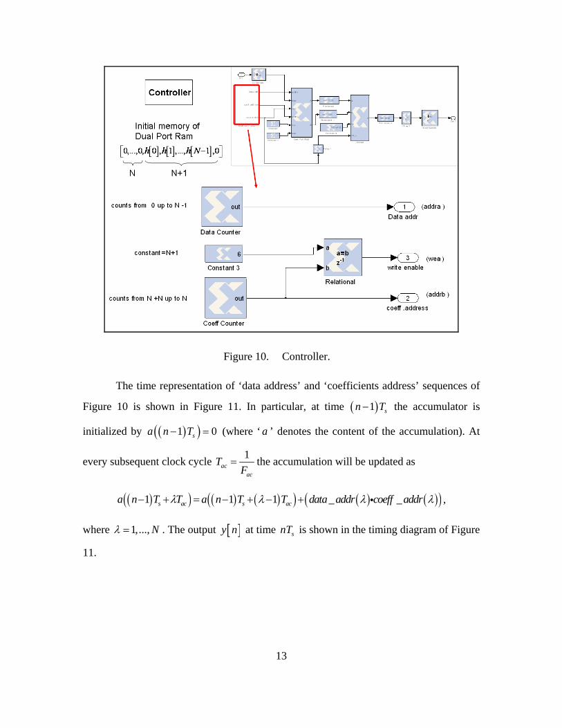
13
Figure 10. Controller.
The time representation of ‘data address’ and ‘coefficients address’ sequences of
Figure 10 is shown in Figure 11. In particular, at time ( )1 sn T− the accumulator is
initialized by ( )( )1 0sa n T− = (where ‘ a ’ denotes the content of the accumulation). At
every subsequent clock cycle 1ac
ac
TF
= the accumulation will be updated as
( )( ) ( ) ( )( ) ( ) ( )( )1 1 1 _ _s ac s aca n T T a n T T data addr coeff addrλ λ λ λ− + = − + − + i ,
where 1,..., Nλ = . The output [ ]y n at time snT is shown in the timing diagram of Figure
11.

14
Figure 11. Time Representation of Simulation.
In what follows we demonstrate the functionality of the design according to the
timing diagram illustrated in Figure 11.
2. Alignment of Data and Filter Coefficients in the Dual Port Ram
The length of the vector x is chosen to be one less than the length of h so that
the writing procedure will introduce a shift by a factor of one in the content of memory
x . It can be inferred that the outcome of the Dual Port Ram is a set of bitstreams, where
the output at port A is a recurrent window of length 1N + (in every sT ) in which the
input data is progressively shifted by one position from left to right, while the bitstream
of port B is a repetition of the vector h . Figure 12 illustrates the outcome of the Dual
Port Ram with time running from right to left.

15
Figure 12. Outcome of Dual Port Ram.
3. Sequential Multiplication and Accumulation (MAC) of Data and Filter Coefficients using DSP48
The output bitstream from the Dual Port Ram, as shown in Figure 12, is being
processed by the DSP48 Xilinx block, which works as a MAC. Its operation mode is
defined as P P A B= + ⋅ (referring to Figure 7) where the product of two pairs of the Dual
Port Ram output ports A and B is being accumulated each time with the previous
product. A reset signal (selected from the DSP48 options) for the outcome P is
introduced at clock rate 1N + provided from the properly delayed ‘write enable’ signal
of the controller of the Dual Port Ram (referring to Figure 9). The adjustment of the delay
is set so that the reset of the outcome P occurs every 1N + times, where a data
coefficient is multiplied with the zero coefficient of vector h .
16
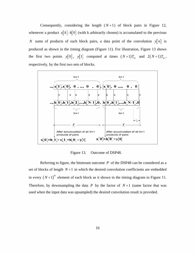
Consequently, considering the length ( 1N + ) of block pairs in Figure 12,
whenever a product [ ] [ ]0x k h⋅ (with k arbitrarily chosen) is accumulated to the previous
N sums of products of each block pairs, a data point of the convolution [ ]y n is
produced as shown in the timing diagram (Figure 11). For illustration, Figure 13 shows
the first two points [ ]0y , [ ]1y computed at times ( )1 acN T+ and ( )2 1 acN T+ ,
respectively, by the first two sets of blocks.
Figure 13. Outcome of DSP48.
Referring to figure, the bitstream outcome P of the DSP48 can be considered as a
set of blocks of length 1N + in which the desired convolution coefficients are embedded
in every ( )1 thN + element of each block as it shown in the timing diagram in Figure 11.
Therefore, by downsampling the data P by the factor of 1N + (same factor that was
used when the input data was upsampled) the desired convolution result is provided.

17
C. RESULTS
In order to test the performance, an FIR filter was designed and tested with two
classes of input signals. In particular the FIR filter has been designed as an Equiripple
Filter with the following characteristics:
Passband: 0-0.2 (in terms of Digital Frequency f )
Stopband: 0.3-0.5 (in terms of Digital Frequency f )
Order: 60
The signals tested are a sinusoid and a white noise. The sinusoid has frequency
0.1 sF F= ⋅ (Hz) with sampling frequency 10000sF = (Hz) and / sf F F= , while the
white noise is sampled at the same rate.
The frequency spectrum of the original signal and the resulting filtered signal for
the sinusoidal case is shown in Figure 14. We can verify that the frequency spectrum of
the original signal remains the same as long as its frequency is within the passband of the
FIR filter.

18
-0.5 -0.4 -0.3 -0.2 -0.1 0 0.1 0.2 0.3 0.4 0.50
200
400
600Frequency Spectrum of Original Signal
Digital Frequency
Am
plitu
de
-0.5 -0.4 -0.3 -0.2 -0.1 0 0.1 0.2 0.3 0.4 0.50
200
400
600Frequency Spectrum of Filtered Signal
Digital Frequency
Am
plitu
de
Figure 14. Frequency Spectrum of the Original and Filtered Signal (Sinusoidal Case).
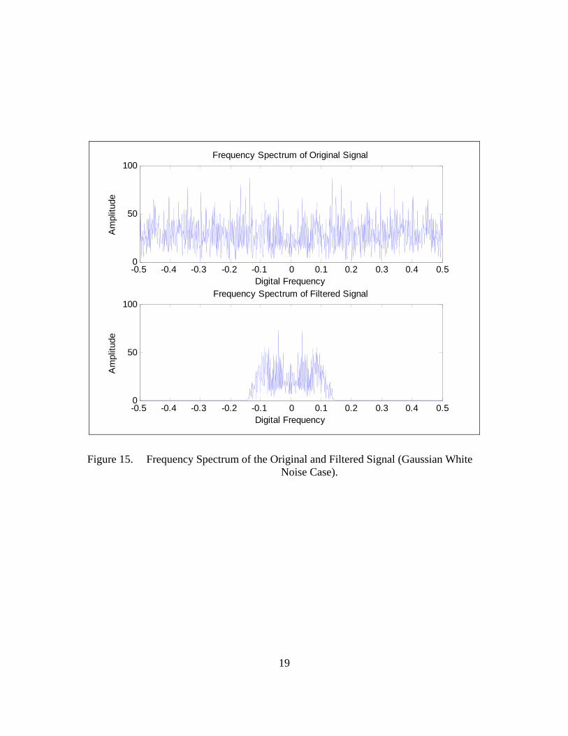
For the Gaussian white noise case the corresponding frequency spectrum, along
with the frequency spectrum of the filtered signal, is depicted in Figure 15. We can
observe that the frequencies of the Gaussian white noise are spread all over the frequency
spectrum while the frequency spectrum of the corresponding filtered signal maintains the
frequencies that are within the passband of the FIR filter and eliminates all the others.
19
-0.5 -0.4 -0.3 -0.2 -0.1 0 0.1 0.2 0.3 0.4 0.50
50
100Frequency Spectrum of Original Signal
Digital Frequency
Am
plitu
de
-0.5 -0.4 -0.3 -0.2 -0.1 0 0.1 0.2 0.3 0.4 0.50
50
100Frequency Spectrum of Filtered Signal
Digital Frequency
Am
plitu
de
Figure 15. Frequency Spectrum of the Original and Filtered Signal (Gaussian White Noise Case).

20
THIS PAGE INTENTIONALLY LEFT BLANK

21
III. DECIMATION BY AN INTEGER FACTOR
A. THEORETICAL PERSPECTIVE
1 Sampling Continuous Time Signals
It is well known that by the sampling theorem, the sampling frequency sF has to
be at least twice the signal bandwidth B [7]. The Discrete Time Fourier Transform of a
sampled signal [ ]x n with actual frequency content F , which is sampled at rate sF , is
given by the following expression:
( ) { } 2j fn
iX f DTFT x n x n e π
+∞−
=−∞⎡ ⎤ ⎡ ⎤⎣ ⎦ ⎣ ⎦= = ∑ , (3.1)
where f is a dimensionless quantity denoting the digital frequency s
FfF
= . From
equation (3.1) we can verify that ( )X f is periodic with period one since
( ) [ ] ( ) [ ] ( )2 1 21 j f n j fn
n nX f x n e x n e X fπ π
+∞ +∞− + −
=−∞ =−∞
+ = = =∑ ∑ .
Therefore, the information is contained in one period (within the interval
1/ 2 1/ 2f− ≤ ≤ ) of the periodic repetition of the frequency spectrum. Figure 16
illustrates the frequency spectrum of a continuous time and sampled signal respectively.
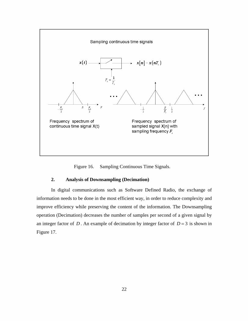
22
Figure 16. Sampling Continuous Time Signals.
2. Analysis of Downsampling (Decimation)
In digital communications such as Software Defined Radio, the exchange of
information needs to be done in the most efficient way, in order to reduce complexity and
improve efficiency while preserving the content of the information. The Downsampling
operation (Decimation) decreases the number of samples per second of a given signal by
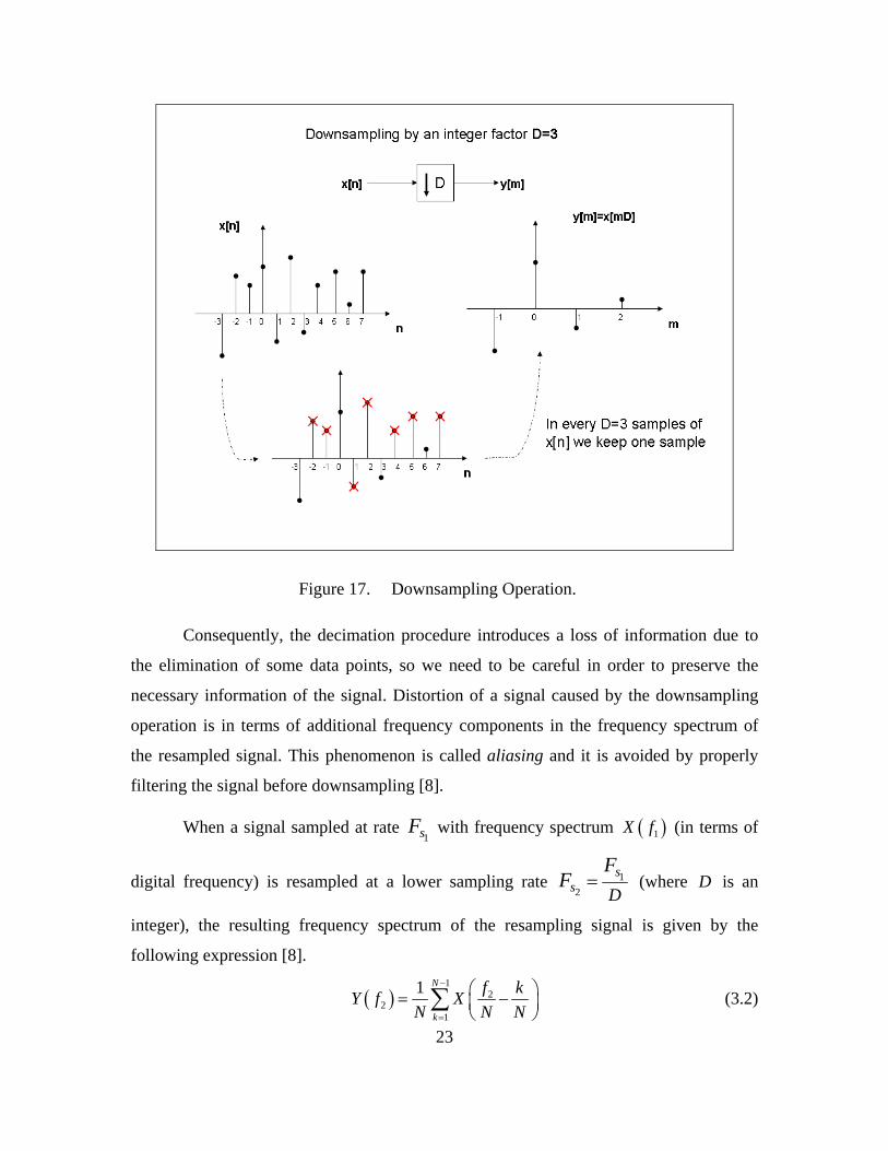
an integer factor of D . An example of decimation by integer factor of 3D = is shown in
Figure 17.
23
Figure 17. Downsampling Operation.
Consequently, the decimation procedure introduces a loss of information due to
the elimination of some data points, so we need to be careful in order to preserve the
necessary information of the signal. Distortion of a signal caused by the downsampling
operation is in terms of additional frequency components in the frequency spectrum of
the resampled signal. This phenomenon is called aliasing and it is avoided by properly
filtering the signal before downsampling [8].
When a signal sampled at rate 1sF with frequency spectrum ( )1X f (in terms of
digital frequency) is resampled at a lower sampling rate 12
ss D
FF = (where D is an
integer), the resulting frequency spectrum of the resampling signal is given by the
following expression [8].
( )1
22
1
1 N
k
f kY f XN N N
−
=
⎛ ⎞= −⎜ ⎟⎝ ⎠
∑ (3.2)

24
From equation (3.2) it is easy to show that no aliasing occurs if the signal has no
frequencies above 12
fD
> , in which case equation (3.2) becomes ( ) 22
1 fY f XN N
⎛ ⎞= ⎜ ⎟⎝ ⎠
[9]. Figure 18 illustrates this concept.
Figure 18. Aliasing Effect in Frequency Spectrum.
Generally, in order to efficiently downsample a noisy signal by an integer factor
of D , with information frequency content within the interval 1 1,2 2D D
⎛ ⎞−⎜ ⎟⎝ ⎠
and without
introducing aliasing, it is necessary to filter the signal first by the appropriate Low Pass
Filter (LPF). Therefore, the useful part of the frequency spectrum will be preserved from
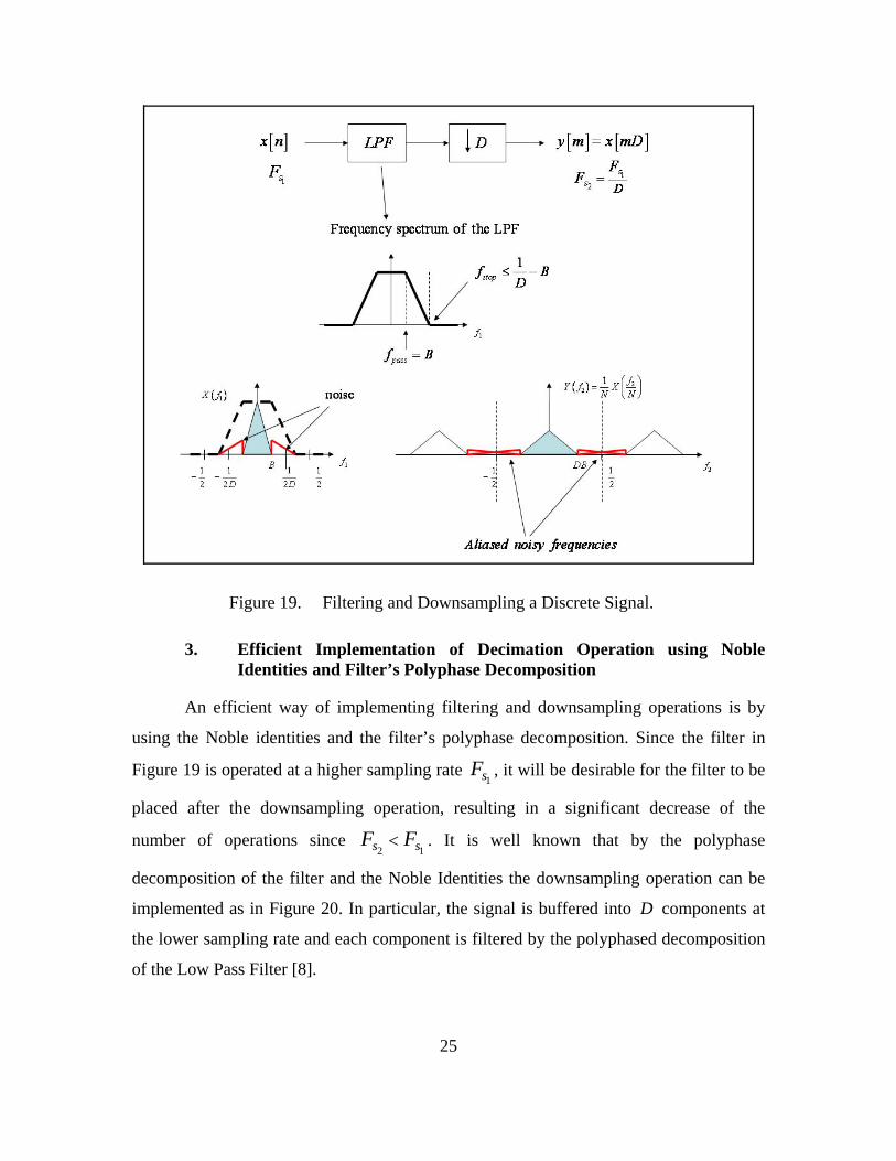
aliased frequencies caused by noise. Figure 19 illustrates this, along with the
specifications of the appropriate Low Pass Filter (LPF).
25
Figure 19. Filtering and Downsampling a Discrete Signal.
3. Efficient Implementation of Decimation Operation using Noble Identities and Filter’s Polyphase Decomposition
An efficient way of implementing filtering and downsampling operations is by
using the Noble identities and the filter’s polyphase decomposition. Since the filter in
Figure 19 is operated at a higher sampling rate 1sF , it will be desirable for the filter to be
placed after the downsampling operation, resulting in a significant decrease of the
number of operations since 2 1s sF F< . It is well known that by the polyphase
decomposition of the filter and the Noble Identities the downsampling operation can be
implemented as in Figure 20. In particular, the signal is buffered into D components at
the lower sampling rate and each component is filtered by the polyphased decomposition
of the Low Pass Filter [8].

26
Figure 20. Efficient Implementation of Decimation.
B. DECIMATION BY TWO WITH FIR MAC AND POLYPHASE DECOMPOSITION
In case of decimation by an integer factor 2D = we can relate the input and
output signal as
[ ] [ ] [ ]2 1
0
2N
ky n h k x n k
−
=
= −∑ , (3.3)
where [ ] ( )sx n x nT= , and sT is the sampling interval. Consequently, the output is
sampled at half the input rate.
The FIR filter polyphase decomposition provides two components, one for the
even samples [ ] [ ]0 2h k h k= and one for the odd samples [ ] [ ]1 2 1h k h k= + . Therefore,
equation (3.3) can be rewritten as
27
[ ] [ ] ( ) [ ] ( )1 1
0 10 0
2 2 1N N
k ky n h k x n k h k x n k
− −
= =
= − + − −⎡ ⎤ ⎡ ⎤⎣ ⎦ ⎣ ⎦∑ ∑ , (3.4)
which breaks down the computation into two phases associated to the even and odd
samples, respectively. Equation (3.4) can be rewritten as
[ ] [ ] [ ] [ ] ( ) [ ] [ ] [ ] ( )1 1
0 0 1 11 1
0 2 2 0 2 1 2 1 .N N
k k
y n h x n h k x n k h x n h k x n k− −
= =
= + − + − − −⎡ ⎤ ⎡ ⎤⎣ ⎦ ⎣ ⎦∑ ∑ (3.5)
Equation (3.5) highlights the fact that, during the time computational interval
( ) ( )2 2 2s sn T t n T− < ≤ the data vector needs to be updated with samples [ ]2 1x n − and
[ ]2x n , while the data in the two summations are available before time ( )2 2 sn T− .
1. Software Implementation
The Simulink/Xilinx implementation needed to perform the decimation-by-two
has the same structure as the model presented in Figure 4 with modified parameters to
match this case. Specifically, the initial values of the vectors of the Dual Port Ram along
with the controller (logic circuit responsible for arranging data points and FIR filter’s
coefficients) are changed in order to implement equation (3.5). Furthermore, the input
data is upsampled at a rate equal to the System Generator’s clock rate and the outcome is
downsampled twice the Sysgen rate, implementing the decimation-by-two operation.
Figure 21 illustrates the structure of this specific design.

28
Figure 21. Downsampling by Two.
In order to test the performance of the simulation a sinusoidal signal is provided
as an input. The input signal is sampled at rate sF while System Generator (Sysgen)
works at a higher sampling rate equal to sNF , with 2 2N − being the degree of the
transfer function of the FIR filter which is decomposed into its polyphase components.
The generation of the polyphase filter is accomplished in the initialization of the
simulation. Since the new system rate provided by Sysgen is higher, the input data is
upsambled by the integer factor of N with the corresponding Xilinx block.
The objective is to achieve a proper alignment of the data and filter’s coefficients
so that they can be applied to a MAC resulting in the decimation-by-two operation.
Towards this goal, we need two memory vectors x and h , containing the data and the
filter coefficients provided by the Dual Port Ram, and a MAC provided by the DSP48.

29
a. Control Logic for Data and Filter Coefficients
The vector h of the filter coefficients is defined as
[ ] [ ] [ ] [ ] [ ] [ ]0 , 2 ,..., 2 2 , 1 , 3 ,..., 2 3 ,0h h h h N h h h N⎡ ⎤= − −⎣ ⎦ and it is the concatenation of
the two polyphase components (one for the even and one for the odd samples) of a
2 1N − length FIR filter (which is generated in MATLAB) with an additional zero at the
end. The vector h has total length 2N and remains unchanged during the operation of
downsampling-by-two. Therefore the ports ‘dinb’ (data input b) and ‘web’ (write enable
b) are set to false. The last zero coefficient of vector h is added in order to serve
computational issues derived from the use of DSP48, which works as a MAC and it will
be explained in the MAC procedure.
The input data vector stored in the first part of the memory of the Dual
Port Ram is a vector x of length 2N and updated at times st nT= as
( ) [ ]2 12
NX n x n
−⎡ ⎤ ←⎣ ⎦ for the even samples and ( ) [ ]2 1
2 1N
X n N x n−
⎡ ⎤− ← −⎣ ⎦ for the odd
samples, with ( )2 10,1,..., 2 2
Nn N
−= − denoting modulo operation. In the implementation,
( )2 1Nn
− is a periodic counter with update rate ac sF NF= . The initial value of the memory
vector x is set to the initial conditions (say zero, for example) and updates its value
according to the corresponding ‘address’ and ‘write enable’ ports provided from the
controller. Figure 22 illustrates the structure of the controller.
30
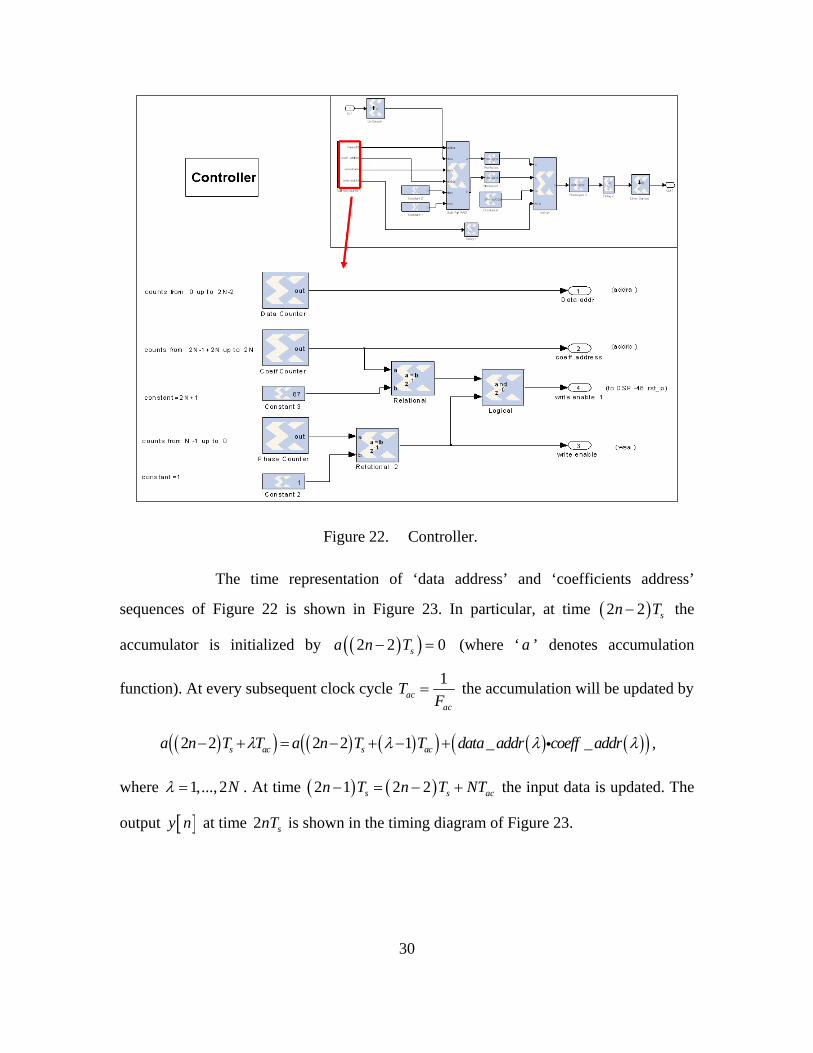
Figure 22. Controller.
The time representation of ‘data address’ and ‘coefficients address’
sequences of Figure 22 is shown in Figure 23. In particular, at time ( )2 2 sn T− the
accumulator is initialized by ( )( )2 2 0sa n T− = (where ‘ a ’ denotes accumulation
function). At every subsequent clock cycle 1ac
ac
TF
= the accumulation will be updated by
( )( ) ( ) ( )( ) ( ) ( )( )2 2 2 2 1 _ _s ac s aca n T T a n T T data addr coeff addrλ λ λ λ− + = − + − + i ,
where 1,..., 2Nλ = . At time ( ) ( )2 1 2 2s s acn T n T NT− = − + the input data is updated. The
output [ ]y n at time 2 snT is shown in the timing diagram of Figure 23.

31
Figure 23. Time Representation of Simulation.
In order to demonstrate the functionality of the implementation, Figure 23
illustrates the timing of the various signals involved.
The outcome of the Dual Port Ram is a set of bitstreams, one from port A
(data points) and one from port B (filter coefficients). It can be inferred that the outcome
of port A is a recurrent window of length 2N , which is subdivided into two windows
(one for the even samples and one for the odd samples of input signal) of length N . At
every time acT both the even and the odd samples are updated, introducing a shift by one
position from left to right. The bitstream of port B is a repetition of the vector h . Figure
24 illustrates the outcome of Dual Port Ram.

32
Figure 24. Outcome of Dual Port Ram.
b. Sequential Multiplication and Accumulation (MAC) of Data and Filter Coefficients using the DSP48
The output bitstream from the Dual Port Ram as it is shown in Figure 24 is
being processed by the DSP48 Xilinx block, which works as a MAC. Its operation mode
is defined by P P A B= + ⋅ (referring to Figure 7) where the product of two output pairs
A and B of the Dual Port Ram, is being accumulated each time with the previous
product. A reset signal (selected from the DSP48 options) for the outcome P is
introduced at clock rate 2N provided from the properly delayed ‘write enable 1’ signal
of the controller of the Dual Port Ram (referring to Figure 22). The adjustment of the
delay is set so that the reset of the outcome P occurs every 2N times, where a data
coefficient is multiplied with the zero coefficient of vector h .
Consequently, considering the length ( )2N of block pairs in figure 24,
after the last product [ ] [ ]0x k h⋅ is accumulated to the previous 2N sums of products of

33
each block pair, a data point of decimation-by-two operation [ ]y n is generated as shown
also in the timing diagram (Figure 23). Figure 25 shows the first two points [ ]0y , [ ]1y
computed at times ( )2 acN T and ( )4 acN T .
Figure 25. Outcome of DSP48.
Referring to Figure 7, the bitstream outcome P of the DSP48 can be
considered as a set of blocks of length 2N in which the desired coefficients of the
decimation-by-two operation are embedded in every ( )2 thN element of each block as
shown in the timing diagram in Figure 23. Therefore, by downsampling the data P by
the factor of 2N (twice the factor that was used when the input data was upsampled) the
desired decimation-by-two operation is performed.

34
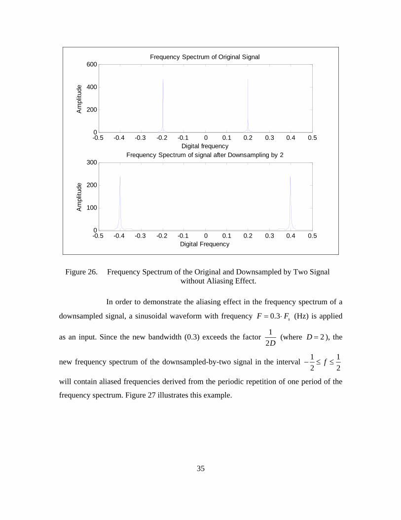
c. Results
In order to test the performance of the simulation a sinusoidal waveform
with frequency 0.2 sF F= ⋅ (Hz) and sampling frequency 1sF = (Hz) is applied as an
input.
The FIR filter has been designed as an Equiripple filter and decomposed
into two polyphase components with the following characteristics:
Passband: 0-0.3 (in terms of Digital Frequency f )
Stopband: 0.4-0.5 (in terms of Digital Frequency f )
Order: 65
The frequency spectrum of the original and the downsampled-by-two
signal is shown in Figure 26. We can verify that the frequency spectrum of the
downsampled-by-two signal is stretched (in terms of the digital frequency) by the integer
factor of two compared to the frequency spectrum of the original signal. Since the
bandwidth of the signal is less than 14
there is no aliasing effect. Therefore, the
frequency of the original signal is 0.2f = while the frequency of the downsampled-by-
two signal is 2 0.2 0.4f = × = (where f is the dimensionless digital frequency).
35
-0.5 -0.4 -0.3 -0.2 -0.1 0 0.1 0.2 0.3 0.4 0.50
200
400
600Frequency Spectrum of Original Signal
Digital frequency
Am
plitu
de
-0.5 -0.4 -0.3 -0.2 -0.1 0 0.1 0.2 0.3 0.4 0.50
100
200
300Frequency Spectrum of signal after Downsampling by 2
Digital Frequency
Am
plitu
de
Figure 26. Frequency Spectrum of the Original and Downsampled by Two Signal without Aliasing Effect.
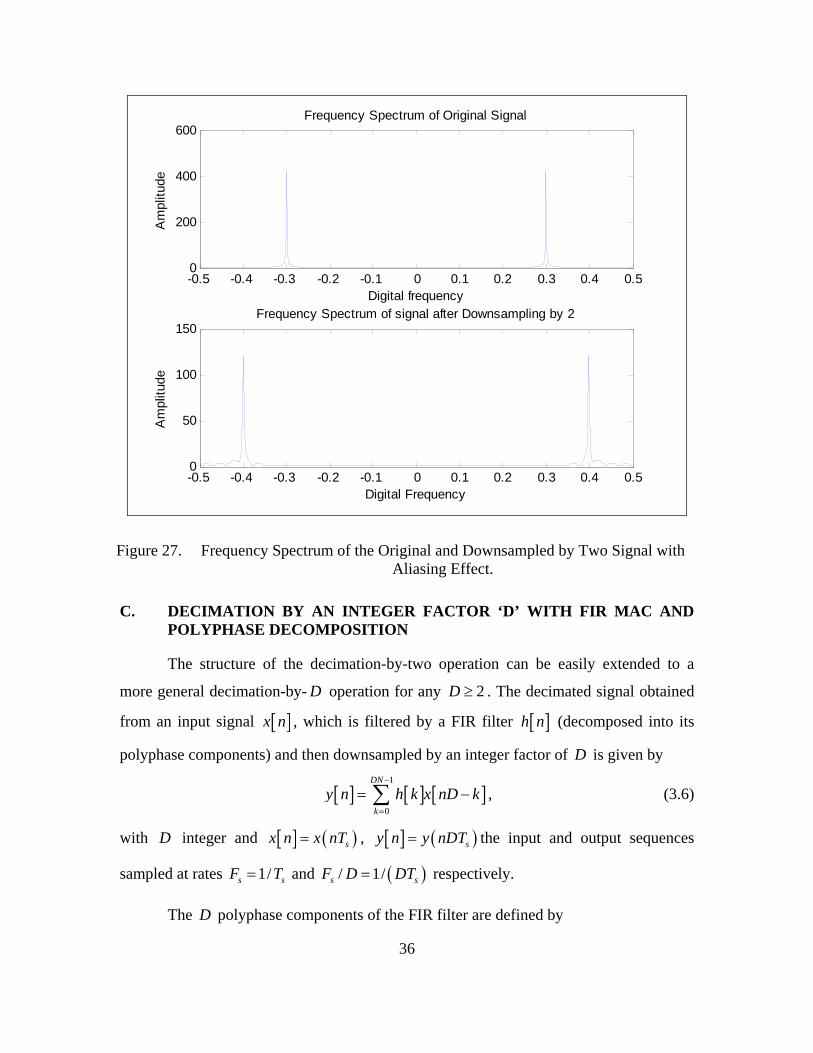
In order to demonstrate the aliasing effect in the frequency spectrum of a
downsampled signal, a sinusoidal waveform with frequency 0.3 sF F= ⋅ (Hz) is applied
as an input. Since the new bandwidth (0.3) exceeds the factor 12D
(where 2D = ), the
new frequency spectrum of the downsampled-by-two signal in the interval 1 12 2
f− ≤ ≤
will contain aliased frequencies derived from the periodic repetition of one period of the
frequency spectrum. Figure 27 illustrates this example.
36
-0.5 -0.4 -0.3 -0.2 -0.1 0 0.1 0.2 0.3 0.4 0.50
200
400
600Frequency Spectrum of Original Signal
Digital frequency
Am
plitu
de
-0.5 -0.4 -0.3 -0.2 -0.1 0 0.1 0.2 0.3 0.4 0.50
50
100
150Frequency Spectrum of signal after Downsampling by 2
Digital Frequency
Am
plitu
de
Figure 27. Frequency Spectrum of the Original and Downsampled by Two Signal with Aliasing Effect.
C. DECIMATION BY AN INTEGER FACTOR ‘D’ WITH FIR MAC AND POLYPHASE DECOMPOSITION
The structure of the decimation-by-two operation can be easily extended to a
more general decimation-by- D operation for any 2D ≥ . The decimated signal obtained
from an input signal [ ]x n , which is filtered by a FIR filter [ ]h n (decomposed into its
polyphase components) and then downsampled by an integer factor of D is given by
[ ] [ ] [ ]1
0
DN
ky n h k x nD k
−
=
= −∑ , (3.6)
with D integer and [ ] ( )sx n x nT= , [ ] ( )sy n y nDT= the input and output sequences
sampled at rates 1/s sF T= and ( )/ 1/s sF D DT= respectively.
The D polyphase components of the FIR filter are defined by

37
[ ] [ ]h k h kD= + , (3.7)
with 0,..., 1D= − and 0,..., 1k N= − . The decimated output is the superposition of the
D phases and it is given by the following expression:
[ ] [ ] ( ) [ ] ( )1 1
0 10 0
1 ...N N
k k
y n h k x n k D h k x n k D− −
= =
= − + − − +⎡ ⎤ ⎡ ⎤⎣ ⎦ ⎣ ⎦∑ ∑
[ ] ( )1
10
... 1N
Dk
h k x n k D D−
−=
+ − − +⎡ ⎤⎣ ⎦∑ . (3.8)
Equation (3.8) can be further decomposed as:
[ ] [ ] [ ] [ ] ( )1
1... 0 ...
N
k
y n h x nD h k x n k D−
=
= + − + − − +⎡ ⎤⎣ ⎦∑ (3.9)
During the time computational interval ( ) ( )s sDn D T t Dn T− < ≤ the data vector
needs to be updated with samples [ ]( 1)x Dn D− − up to [ ]x Dn , while the data in the D
summations are available before time ( ) sDn D T− .
The design needed to perform the decimation-by- D operation is similar to the
decimation-by-two case. The memory vector for the input data points in the Dual Port
Ram has length 1DN − and updates its value by
( ) [ ]( ) [ ]
( ) [ ]
( )( ) [ ]
1
1
1
1
,
1 ,
,
1 1 .
...
...
DN
DN
DN
DN
X n x nD
X n N x nD
X n N x nD
X n D N x nD D
−
−
−
−
⎡ ⎤ ←⎣ ⎦⎡ ⎤− ← −⎣ ⎦
⎡ ⎤− ← −⎣ ⎦
⎡ ⎤− − ← − +⎣ ⎦
The FIR filter coefficients vector, which is stored in the second memory of the
Dual Port Ram is the concatenation of its polyphase components derived from expression
(3.7) with total length 1DN − .

38
In the implementation, ( ) 10,..., 2
DNn DN
−= − is a periodic counter with update
rate ac sF NF= , which is the clock rate of the System Generator. Therefore the input data
is upsampled by the integer factor of N .
The time representation of ‘data address’ and ‘coefficients address’ sequences are
shown in Figure 28. In particular, at time ( ) sDn D T− the accumulator is initialized as
( )( ) 0sa Dn D T− = (where ‘ a ’ denotes the accumulation function). At every subsequent
clock cycle 1ac
ac
TF
= the accumulation will be updated by
( )( ) ( ) ( )( ) ( ) ( )( )1 _ _s ac s aca Dn D T T a Dn D T T data addr coeff addrλ λ λ λ− + = − + − + i ,
where 1,..., DNλ = . The input data is updated every thN multiple of acT with total
multiples DN . In particular, ( ) ( )1 s s acDn D T Dn D T NT− + = − + . The output [ ]y n at
time sDnT is shown in the timing diagram of Figure 28.
Figure 28. Timing Diagram for Decimation by D.

39
Apart from the new vectors that are stored in the Dual Port Ram, this design can
be obtained by simple extension of the decimation-by-two case to the more general
decimation-by-D.
Referring to Figure 7, the bitstream outcome P of the DSP48 can be considered
as a set of blocks of length DN in which the desired coefficients of the decimation-by- D
operation are embedded in every ( )thDN element of each block as shown in the timing
diagram in Figure 28. Therefore by downsampling the data P by the factor of DN ( D
times the factor which was used when the input data was upsampled) the desired
decimation-by-D operation is performed.
In order to test the performance of the simulation for the decimation factor 4D =
a sinusoidal waveform with frequency 0.1 sF F= ⋅ (Hz) and sampling frequency 1sF =
(Hz) is applied as an input.
The FIR filter has been designed as an Equiripple filter and decomposed into four
polyphase components with the following characteristics:
Passband: 0-0.2 (in terms of Digital Frequency f )
Stopband: 0.25-0.5 (in terms of Digital Frequency f )
Order: 29
The frequency spectrum of the original and the downsampled by 4D = signal is
shown in Figure 29. We can verify that the frequency spectrum of the downsampled
signal is stretched (in terms of the digital frequency) by the integer factor of four
compared to the frequency spectrum of the original signal. Since the initial bandwidth of
the signal is less than 12D
there is no aliasing effect. Therefore, the frequency of the
original signal is 0.1f = , while the frequency of the decimation-by-four signal is
4 0.1 0.4f = × = , where f is the dimensionless digital frequency.

40
-0.5 -0.4 -0.3 -0.2 -0.1 0 0.1 0.2 0.3 0.4 0.50
200
400
600Frequency Spectrum of Original Signal
Digital frequency
Am
plitu
de
-0.5 -0.4 -0.3 -0.2 -0.1 0 0.1 0.2 0.3 0.4 0.50
100
200
300Frequency Spectrum of signal after Downsample by 4
Digital Frequency
Am
plitu
de
Figure 29. Frequency Spectrum of the Original and Downsampled by 4D = Signal.

41
IV. INTERPOLATION BY AN INTEGER FACTOR
A. THEORETICAL PERSPECTIVE
1. Analysis of Upsampling (Interpolation)
In Software Defined Radios (SDR), the modulation process is performed in the
digital domain. The data rate of the transmitted information needs to be increased in order
to match the rate of the modulation (carrier frequency). An upsample operation
(interpolation) increases the number of samples per second of a given signal by an integer
factor D . An example of interpolation by integer factor of 3D = is shown in Figure 30.
Figure 30. Upsampling Operation.
42
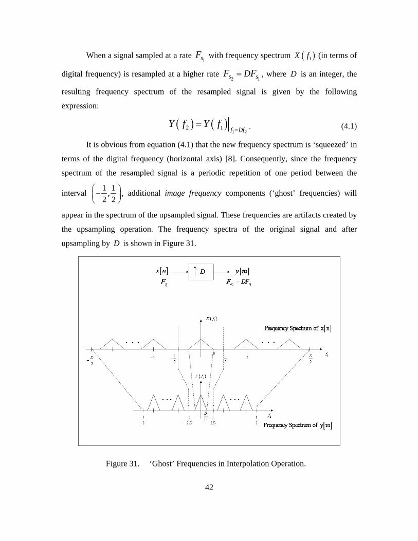
When a signal sampled at a rate 1sF with frequency spectrum ( )1X f (in terms of
digital frequency) is resampled at a higher rate 2 1s sDF F= , where D is an integer, the
resulting frequency spectrum of the resampled signal is given by the following
expression:
( ) ( )1 2
2 1 f DfY f Y f
== . (4.1)
It is obvious from equation (4.1) that the new frequency spectrum is ‘squeezed’ in
terms of the digital frequency (horizontal axis) [8]. Consequently, since the frequency
spectrum of the resampled signal is a periodic repetition of one period between the
interval 1 1,2 2
⎛ ⎞−⎜ ⎟⎝ ⎠
, additional image frequency components (‘ghost’ frequencies) will
appear in the spectrum of the upsampled signal. These frequencies are artifacts created by
the upsampling operation. The frequency spectra of the original signal and after
upsampling by D is shown in Figure 31.
Figure 31. ‘Ghost’ Frequencies in Interpolation Operation.

43
In order to eliminate the ‘ghost’ frequencies a Low Pass Filter (LPF) is needed
after the upsampling operation. The frequency response of the LPF along with its
specifications is depicted in Figure 32.
Figure 32. Upsampling and Filtering with LPF.
2. Efficient Implementation of Interpolation Operation using Noble Identities and Filter’s Polyphase Decomposition
An efficient way of implementing upsampling and filtering operations is by using
the Noble identities with the filter’s polyphase decomposition. Since the filter in Figure
32 is operated at a higher sampling rate 2sF it would be desirable for the filter to be
placed before the upsampling operation, thus minimizing the cost. It can be shown that
the upsampling operation shown in Figure 32, with the LPF ( ) ( )0
Nn
nH z h n z−
=
=∑ , can be
44
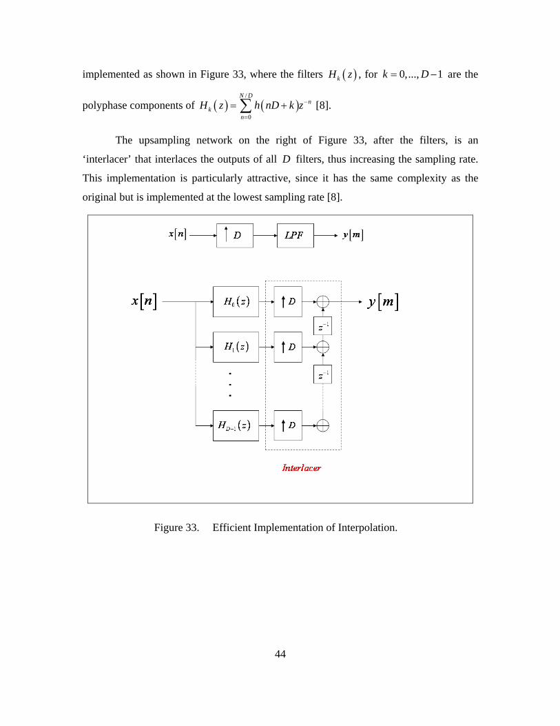
implemented as shown in Figure 33, where the filters ( )kH z , for 0,..., 1k D= − are the
polyphase components of ( ) ( )/
0
N Dn
kn
H z h nD k z−
=
= +∑ [8].
The upsampling network on the right of Figure 33, after the filters, is an
‘interlacer’ that interlaces the outputs of all D filters, thus increasing the sampling rate.
This implementation is particularly attractive, since it has the same complexity as the
original but is implemented at the lowest sampling rate [8].
Figure 33. Efficient Implementation of Interpolation.

45
B. INTERPOLATION BY TWO WITH FIR MAC AND POLYPHASE DECOMPOSITION
From the polyphase decomposition the upsampling by two is determined as
[ ] [ ] [ ]
[ ] [ ] [ ]
1
00
1
10
2 ,
2 1 .
N
kN
k
y n h k x n k
y n h k x n k
−
=
−
=
= −
+ = −
∑
∑ (4.2)
Here [ ] [ ]0 2h k h k= and [ ] [ ]1 2 1h k h k= + are the polyphase components (even and odd
samples) of the filter [ ]h n while [ ] ( )sx n x nT= with sT the sampling interval. Consequently, the output rate is twice the input rate.
Equation (4.2) highlights the fact that the signal [ ]x n is interpolated by
interlacing two signals, [ ]2y n and [ ]2 1y n + , which are computed independently.
1. Software Implementation
The Simulink/Xilinx implementation needed to perform the interpolation-by-two
has the same structure as the model presented in Figure 4 with parameters properly
chosen to match the new case. Specifically the initial values of the vectors of the Dual
Port Ram along with the controller (logic circuit responsible for arranging data points and
FIR filter’s coefficients) are changed in order to implement equation (4.2). Furthermore,
the input data is upsampled at a rate equal to the System Generator’s clock rate and the
outcome is downsampled at the half of the Sysgen rate, implementing the interpolation-
by-two operation. Figure 34 illustrates this design.

46
Figure 34. Upsampling by Two.
In order to test the performance of the simulation, a sinusoidal signal is provided
as an input. The input signal is sampled at rate sF , while the System Generator (Sysgen)
works at a higher sampling rate equal to ( )2 1 sN F+ , with 2 2N − being the degree of the
transfer function of the FIR filter which is decomposed into its polyphase components.
The generation of the polyphase filter is accomplished in the initialization of the
simulation. Since the new system rate provided by Sysgen is higher, the input data is
upsambled by the integer factor of ( )2 1N + with the corresponding Xilinx block.
The objective is to achieve a proper alignment of the data and filter’s coefficients
so that they can be applied to a MAC resulting in the interpolation-by-two operation.
Towards this goal, we need two memory vectors x and h containing the data and the
filter coefficients respectively provided by the Dual Port Ram and a MAC provided by
the DSP48.

47
a. Control Logic for Data and Filter Coefficients
The vector h of the filter coefficients is defined as
[ ] [ ] [ ] [ ] [ ] [ ]0 , 2 ,..., 2 2 ,0,0, 1 , 3 ,..., 2 3 ,0h h h h N h h h N⎡ ⎤= − −⎣ ⎦ and it is the concatenation
of the two polyphase components (one for the even and one for the odd samples) of a
2 1N − length FIR filter (which is generated in MATLAB) with three properly placed
additional zeros. The length of the vector h is 2 2N + and its value remains unchanged
during the operation of upsampling-by-two. Therefore the ports ‘dinb’ (data input b) and
‘web’ (write enable b) are set to false. The zero coefficients are required by
computational issues derived from the controller and the use of the DSP48 block which
works as a MAC and it will be explained in the MAC procedure.
The input data vector stored in the first part of the memory of the Dual
Port Ram is a vector x of length N and it is updated as ( ) [ ]NX n x n⎡ ⎤ ←⎣ ⎦ . The data
address counter is defined as ( ) 0,1,..., 1N
n N= − and it is repeated twice during the
sampling interval sT . The initial value of the memory vector x is set to the initial
conditions (say zero, for example) and updates its value according to the corresponding
‘address’ and ‘write enable’ ports provided from the controller. Figure 35 illustrates the
controller of the simulation.

48
Figure 35. Controller.
The time representation of ‘data address’ and ‘coefficients address’
sequences of Figure 35 are shown in Figure 36. In particular, at time ( )2 2 sn T− the
accumulator is initialized as ( )( )2 2 0sa n T− = (where a denotes the content of the
accumulation). At every subsequent clock cycle 1ac
ac
TF
= , the accumulation will be
updated by
( )( ) ( ) ( )( ) ( ) ( )( )2 2 2 2 1 _ _s ac s aca n T T a n T T data addr coeff addrλ λ λ λ− + = − + − + i , and
( )( ) ( ) ( )( ) ( ) ( )( )2 1 2 1 1 _ _s ac s aca n T T a n T T data addr coeff addrλ λ λ λ− + = − + − + i ,

49
with 1,..., Nλ = . The outputs [ ]2 1y n − , [ ]2y n at times ( )2 1 sn T− and 2 snT respectively
are shown in the timing diagram of Figure 36. .
Figure 36. Time Representation of Simulation.
In order to demonstrate the functionality of the implementation, Figure 36
illustrates the timing of the various signals involved.
The outcome of the Dual Port Ram is a set of bitstreams, one from port A
(data points) and one for port B (filter’s coefficients). The bitstream of port B is a
repetition of the vector h . It can be inferred that the outcome of port A is a recurrent
window of length 2 2N + , which is subdivided into two windows of length 1N + . At
every time acT both subwindows are updated with the same data, introducing a shift by
one position from left to right, while the first subwindow starts updating from the second
sample. Figure 37 illustrates the outcome of the Dual Port Ram.

50
Figure 37. Outcome of Dual Port Ram.
b. Sequential Multiplication and Accumulation (MAC) of Data and Filter Coefficients using DSP48
The output bitstream from the Dual Port Ram, as it is shown in Figure 37,
is being processed by the DSP48 Xilinx block, which implements the MAC. Its operation
mode is defined by P P A B= + ⋅ (referring to Figure 7), where the product of two pairs
of Dual Port Ram output ports A and B is being accumulated each time with the previous
product. A reset signal (selected from the DSP48 options) for the outcome P is
introduced at clock rate 1N + provided from the properly delayed ‘write enable 1’ signal
of the controller of the Dual Port Ram (referring to Figure 35). The adjustment of the
delay is set so that the reset of the outcome P occurs every 1N + samples, where the
coefficients of vector h are zero, without affecting the accumulation procedure of the
interpolation-by-two operation and therefore there is no loss of information. The third

51
zero coefficient of vector h which is placed at the first odd sample is not affecting the
accumulation process of the interpolation-by-two operation as well, since the first
subwindow of the data vector is updated from the second sample.
Consequently, considering the length ( )2 2N + of block pairs in Figure
37, whenever a product [ ] [ ]0x k h⋅ is accumulated to the previous 2 1N + sums of
products of each block pair, two data points of interpolation-by-two operation [ ]y n are
provided at every ( )1 acN T+ interval as it also shown in the timing diagram in Figure 36.
Figure 38 shows the first three points [ ]0y , [ ]1y , [ ]2y provided at time
( )1 acN Tμ + ,where 1,2,3μ = .
Figure 38. Outcome of DSP48.

52
Referring to Figure 7, the bitstream outcome P of the DSP48 can be
considered as a set of blocks of length 2 2N + in which the desired coefficients of the
interpolation-by-two operation are embedded in every ( )1 thN + and ( )2 2 thN + element
of each block as it shown in the timing diagram in Figure 36. Therefore by downsampling
the data P by the factor 1N + (half the factor that was used when the input data was
upsampled) the desired interpolation-by-two operation is performed.
c. Results
In order to test the performance of the simulation a sinusoidal waveform
with frequency 0.4 sF F= ⋅ (Hz) and sampling frequency 1sF = (Hz) is applied as an
input.
The FIR filter has been designed as an Equiripple filter and decomposed
into two polyphase components with the following characteristics:
Passband: 0-0.4 (in terms of Digital Frequency f )
Stopband: 0.45-0.5 (in terms of Digital Frequency f )
Order: 31
The frequency spectrum of the original and the upsampled-by-two signal
is shown in Figure 39. We can verify that the frequency spectrum of the upsampled-by-
two signal is squeezed (in terms of the digital frequency) by the integer factor of two
compared to the frequency spectrum of the original signal. Therefore, the frequency of
the original signal is 0.4f = while the frequency of the upsampled-by-two signal is
0.4 / 2 0.2f = = (where f is the dimensionless digital frequency).
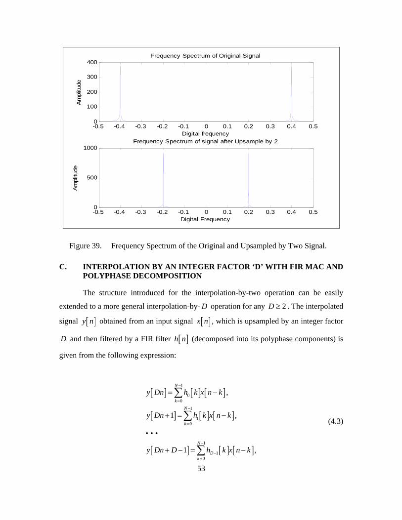
53
-0.5 -0.4 -0.3 -0.2 -0.1 0 0.1 0.2 0.3 0.4 0.50
100
200
300
400Frequency Spectrum of Original Signal
Digital frequency
Am
plitu
de
-0.5 -0.4 -0.3 -0.2 -0.1 0 0.1 0.2 0.3 0.4 0.50
500
1000Frequency Spectrum of signal after Upsample by 2
Digital Frequency
Am
plitu
de
Figure 39. Frequency Spectrum of the Original and Upsampled by Two Signal.
C. INTERPOLATION BY AN INTEGER FACTOR ‘D’ WITH FIR MAC AND POLYPHASE DECOMPOSITION
The structure introduced for the interpolation-by-two operation can be easily
extended to a more general interpolation-by- D operation for any 2D ≥ . The interpolated
signal [ ]y n obtained from an input signal [ ]x n , which is upsampled by an integer factor
D and then filtered by a FIR filter [ ]h n (decomposed into its polyphase components) is
given from the following expression:
[ ] [ ] [ ]
[ ] [ ] [ ]
[ ] [ ] [ ]
1
00
1
10
1
10
,
1 ,
1 ,
N
kN
k
N
Dk
y Dn h k x n k
y Dn h k x n k
y Dn D h k x n k
−
=
−
=
−
−=
= −
+ = −
+ − = −
∑
∑
∑
i i i (4.3)
54
with D integer and [ ] ( )sx n x nT= , [ ] ( )/sy n y nT D= the input and output sequences
sampled at rates 1/s sF T= and /s sDF D T= respectively.
The D polyphase components of the FIR filter are defined as:
[ ] [ ]h k h kD= + (4.4)
with 0,..., 1D= − and 0,..., 1k N= − .
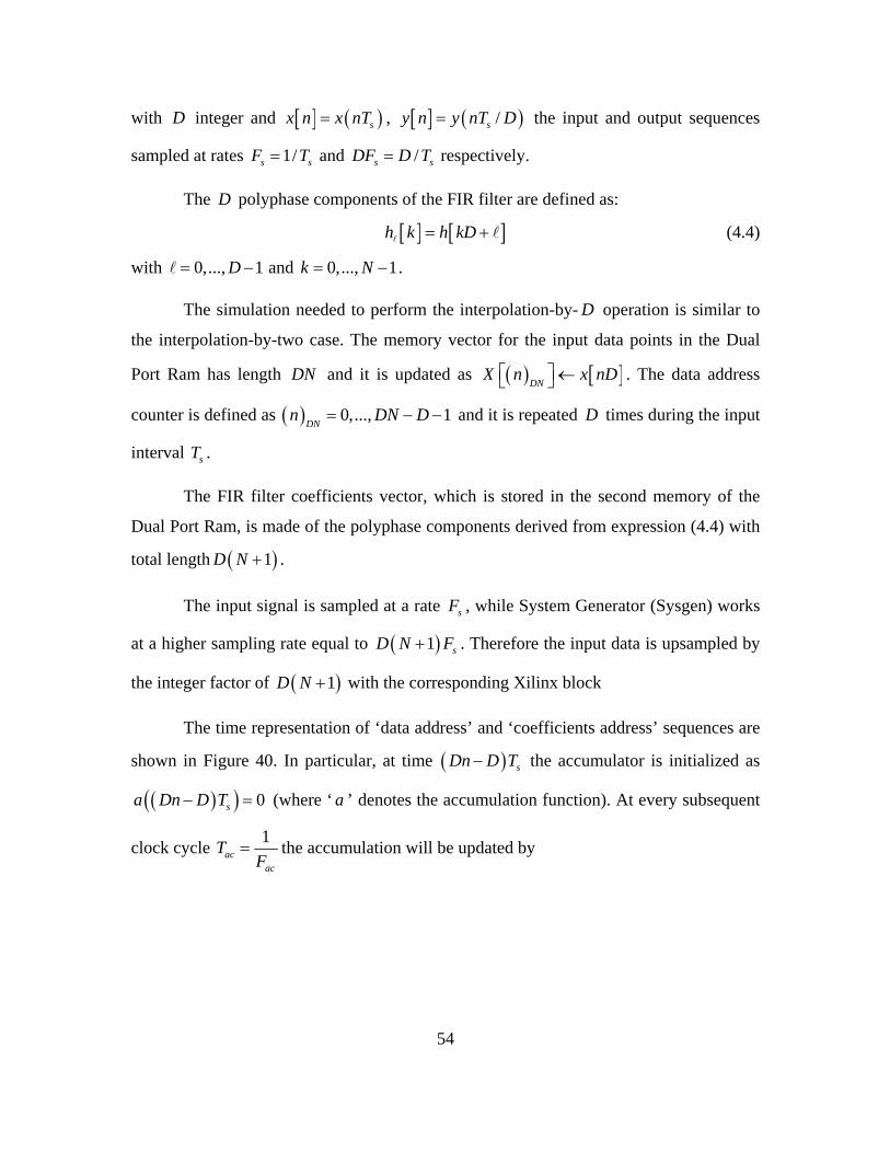
The simulation needed to perform the interpolation-by- D operation is similar to
the interpolation-by-two case. The memory vector for the input data points in the Dual
Port Ram has length DN and it is updated as ( ) [ ]DNX n x nD⎡ ⎤ ←⎣ ⎦ . The data address
counter is defined as ( ) 0,..., 1DN
n DN D= − − and it is repeated D times during the input
interval sT .
The FIR filter coefficients vector, which is stored in the second memory of the
Dual Port Ram, is made of the polyphase components derived from expression (4.4) with
total length ( )1D N + .
The input signal is sampled at a rate sF , while System Generator (Sysgen) works
at a higher sampling rate equal to ( )1 sD N F+ . Therefore the input data is upsampled by
the integer factor of ( )1D N + with the corresponding Xilinx block
The time representation of ‘data address’ and ‘coefficients address’ sequences are
shown in Figure 40. In particular, at time ( ) sDn D T− the accumulator is initialized as
( )( ) 0sa Dn D T− = (where ‘ a ’ denotes the accumulation function). At every subsequent
clock cycle 1ac
ac
TF
= the accumulation will be updated by
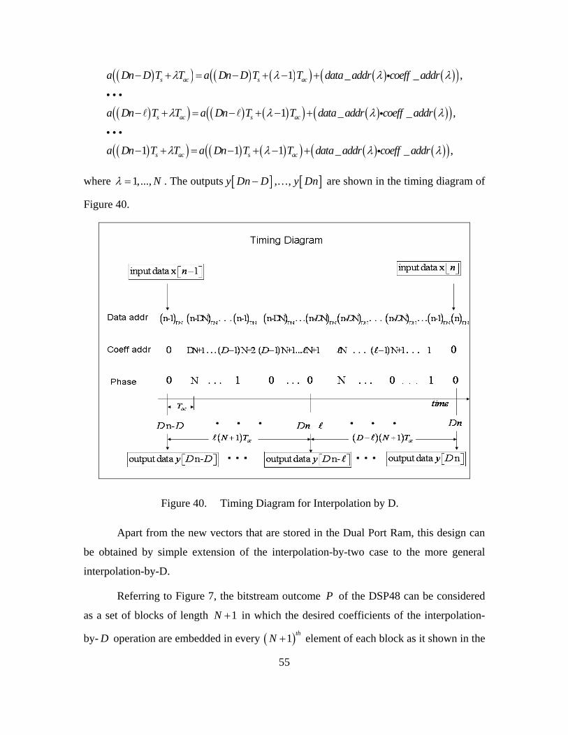
55
( )( ) ( ) ( )( ) ( ) ( )( )
( )( ) ( ) ( )( ) ( ) ( )( )
( )( ) ( ) ( )( ) ( ) ( )( )
1 _ _ ,
1 _ _ ,
1 1 1 _ _ ,
s ac s ac
s ac s ac
s ac s ac
a Dn D T T a Dn D T T data addr coeff addr
a Dn T T a Dn T T data addr coeff addr
a Dn T T a Dn T T data addr coeff addr
λ λ λ λ
λ λ λ λ
λ λ λ λ
− + = − + − +
− + = − + − +
− + = − + − +
i
i i ii
i i ii
where 1,..., Nλ = . The outputs [ ]y Dn D− ,…, [ ]y Dn are shown in the timing diagram of
Figure 40.
Figure 40. Timing Diagram for Interpolation by D.
Apart from the new vectors that are stored in the Dual Port Ram, this design can
be obtained by simple extension of the interpolation-by-two case to the more general
interpolation-by-D.
Referring to Figure 7, the bitstream outcome P of the DSP48 can be considered
as a set of blocks of length 1N + in which the desired coefficients of the interpolation-
by- D operation are embedded in every ( )1 thN + element of each block as it shown in the
56
timing diagram in Figure 40. Therefore by downsampling the data P by the factor of
1N + ( D times less the factor which was used when the input data was upsampled) the
desired interpolation-by- D operation is performed.
In order to test the performance of the simulation for interpolation factor , 4D = a
sinusoidal waveform with frequency 0.4 sF F= ⋅ (Hz) and sampling frequency 1sF =
(Hz) is applied as an input.
The FIR filter has been designed as an Equiripple filter and decomposed into four
polyphase components with the following characteristics:
Passband: 0-0.2 (in terms of Digital Frequency f )
Stopband: 0.25-0.5 (in terms of Digital Frequency f )
Order: 120
The frequency spectrum of the original and the upsampled by 4D = signal is
shown in Figure 41. We can verify that the frequency spectrum of the upsampled by
4D = signal is squeezed (in terms of the digital frequency) by the integer factor of four
compared to the frequency spectrum of the original signal. Therefore, the frequency of
the original signal is 0.4f = , while the frequency of the upsampled-by-four signal is
0.4 / 4 0.1f = = (where f is the dimensionless digital frequency).
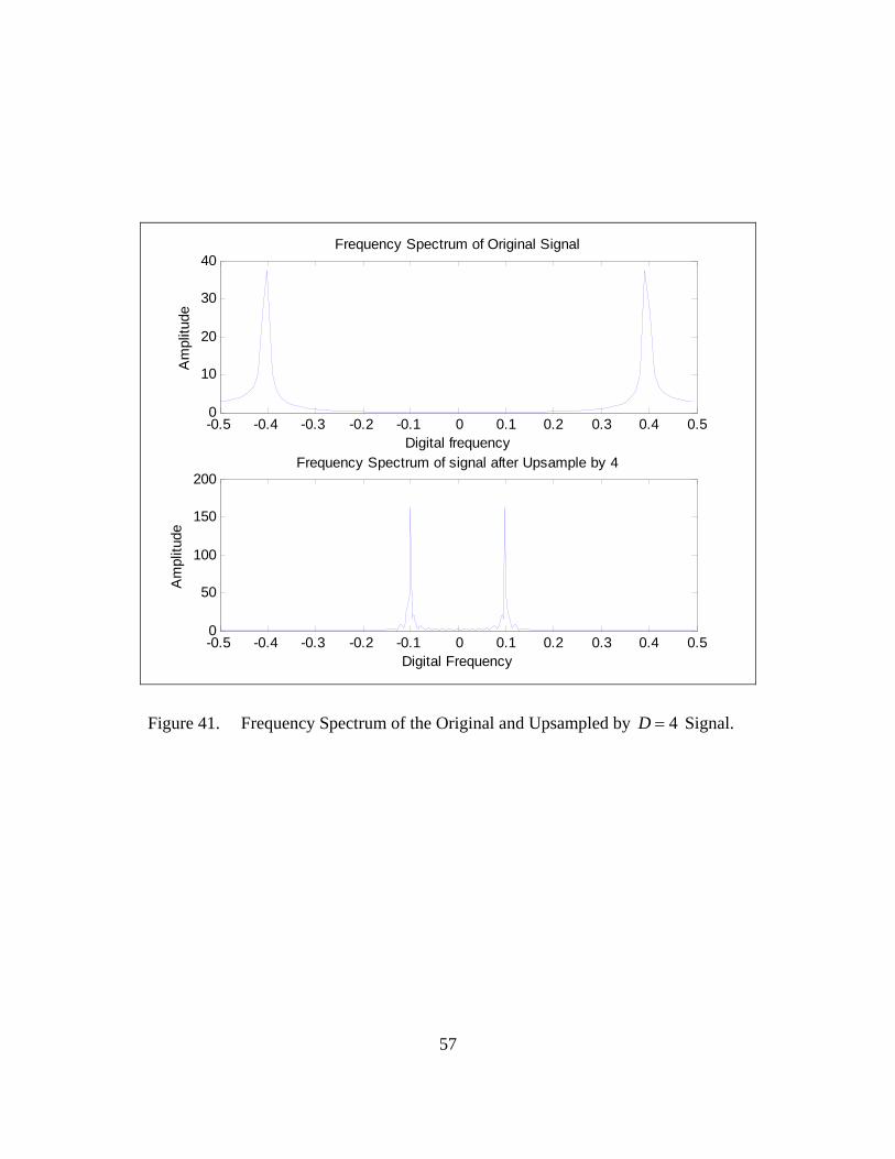
57
-0.5 -0.4 -0.3 -0.2 -0.1 0 0.1 0.2 0.3 0.4 0.50
10
20
30
40Frequency Spectrum of Original Signal
Digital frequency
Am
plitu
de
-0.5 -0.4 -0.3 -0.2 -0.1 0 0.1 0.2 0.3 0.4 0.50
50
100
150
200Frequency Spectrum of signal after Upsample by 4
Digital Frequency
Am
plitu
de
Figure 41. Frequency Spectrum of the Original and Upsampled by 4D = Signal.

58
THIS PAGE INTENTIONALLY LEFT BLANK

59
V. CONCLUSIONS
A. SUMMARY OF THE WORK
In this research, we presented an architecture for implementing resampling
operations in FPGAs. The particularly interesting feature of this approach is the use of a
specific functional block (the DSP48), which is optimized for DSP applications in real
time. Although a number of applications are possible, this approach is particularly
attractive in the implementation of Software Defined Radios (SDR).
Three classes of DSP operations have been implemented software in the Simulink
design environment:
1) Finite Impulse Response filter
2) Decimation by an integer factor
3) Interpolation by an integer factor
All subsystems of the design are fully accessible by the designer at every stage.
The key ingredient was the use of a Multiplier and Accumulator (MAC)
architecture carried out from the DSP48 slice, which is an efficient Xilinx block (from
the Simulink library) for many DSP applications. The dual input fed to the DSP48 was
provided from the Dual Port Ram Xilinx block, which is a memory device that allows the
user to specify the width and the values for each memory part in order to perform the
three above mentioned operations.
The Xilinx System Generator was used to realize the software performance to a
Virtex-4 FPGA, increasing the computation data rate according to each case.
MATLAB code was used to generate the FIR filter and its polyphase
decomposition in the design and also to verify the performance providing the desired
results in terms of plots demonstrating the corresponding theoretical perspective.
60
B. SUGGESTION FOR FUTURE WORK
The designs presented in this thesis will be part of a general Software Defined
Radio (SDR) implementation. In particular it will be interlaced with both modulation and
demodulation processes, so that the whole radio will be implemented in software.
There are several issues to be addressed. The most important is whether this
approach can be implemented in real time using a reasonable amount of chip “real
estate”. In order to address this problem, higher-level language code needs to be used to
implement the algorithm on the chip.
This is part of an ongoing research project.

61
LIST OF REFERENCES
[1] Jeffrey H. Reed, Software Radio: A modern approach to Radio Engineering, Prentice Hall, 2002.
[2] Ruđer Bošković Institute, http://www.irb.hr/en/cir/education/courses/fpga/FPGA/fpga_sklopovi/ (Accessed August 12, 2008).
[3] Xilinx online documentation, System Generator for DSP, User Guide, Release 10.1.1, April 2008 http://www.xilinx.com/support/documentation/sw_manuals/sysgen_user.pdf (Accessed August 12, 2008).
[4] ARM webpage (photo of FPGA Virtex-4 embedded in processing board) http://www.arm.com/rximages/15515.jpg (Accessed November 7, 2008).
[5] Xilinx online documentation, System Generator for DSP, Reference Guide, Release 10.1.1, April 2008, http://www.xilinx.com/support/documentation/sw_manuals/sysgen_ref.pdf (Accessed August 17, 2008).
[6] Xilinx online documentation, System Generator for DSP, Getting Started Guide, Release 10.1.1, April 2008, http://www.xilinx.com/support/documentation/sw_manuals/sysgen_gs.pdf, (Accessed August 20, 2008).
[7] Robert D. Strum, Donald E. Kirk, First Principles of Discrete Systems and Digital Signal Processing, 1988.
[8] Roberto Cristi, Modern Digital Signal Processing. Thomson Brooks/Cole, 2004.
[9] P. P. Vaidyanathan, Multirate Systems and Filter Banks, Prentice Hall, 1993.
[10] Xilinx online documentation, Xtreme DSP for Virtex-4 FPGAs, User Guide, UG073(v2.7) May 15,2008 http://www.xilinx.com/support/documentation/user_guides/ug073.pdf (Accessed July 18, 2008)
[11] Ondřej Pirochta, “Hardware Implementations of Digital Filters in FPGA”, Brno University of Technology http://www.urel.feec.vutbr.cz/ra2008/archive/ra2005/papers/401.pdf (Accessed November 20, 2008)

62
THIS PAGE INTENTIONALLY LEFT BLANK

63
INITIAL DISTRIBUTION LIST
1. Defense Technical Information Center Ft. Belvoir, Virginia
2. Dudley Knox Library Naval Postgraduate School Monterey, California
3. Professor Roberto Cristi Naval Postgraduate School Monterey, California
4. Associate Professor Craig W. Rasmussen Naval Postgraduate School Monterey, California
5. Embassy of Greece Office of Naval Attaché
Washington DC 20008