Nanoelectronics 09 - University of York
15
Department of Electronic Engineering Nanoelectronics 09 Atsufumi Hirohata 10:00 Wednesday , 16/February /2022 (D/L 006) Quick Review over the Last Lecture ( ) : ( ) : ( Single electron transistor (SET) ) : * http://stc-mditr.org/research/lsoe/highlights/highlight4.cfm ON ( Drain ) current increases with increasing a ( gate ) voltage. * OFF p n
Transcript of Nanoelectronics 09 - University of York

Department of Electronic Engineering
Nanoelectronics09
Atsufumi Hirohata
10:00 Wednesday, 16/February/2022 (D/L 006)
Quick Review over the Last Lecture( Field effect transistor (FET) ) :
( Esaki Tunneling diode ) : ( Single electron transistor (SET) ) :
* http://stc-mditr.org/research/lsoe/highlights/highlight4.cfm
ON
( Drain ) current increases with increasing a ( gate ) voltage. *
OFF
p n
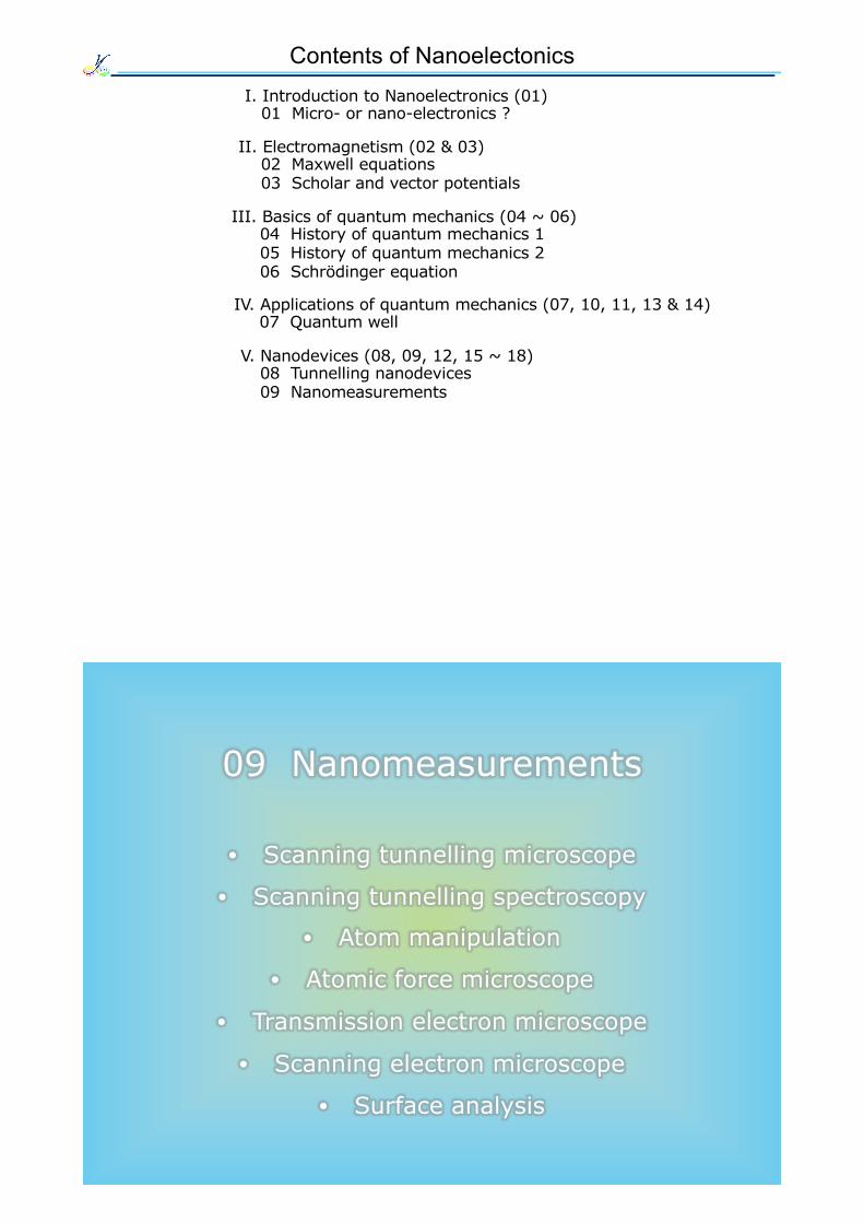
Contents of NanoelectonicsI. Introduction to Nanoelectronics (01)
01 Micro- or nano-electronics ?
II. Electromagnetism (02 & 03)02 Maxwell equations03 Scholar and vector potentials
III. Basics of quantum mechanics (04 ~ 06)04 History of quantum mechanics 105 History of quantum mechanics 206 Schrödinger equation
IV. Applications of quantum mechanics (07, 10, 11, 13 & 14)07 Quantum well
V. Nanodevices (08, 09, 12, 15 ~ 18)08 Tunnelling nanodevices09 Nanomeasurements
09 Nanomeasurements
• Scanning tunnelling microscope
• Scanning tunnelling spectroscopy
• Atom manipulation
• Atomic force microscope
• Transmission electron microscope
• Scanning electron microscope
• Surface analysis
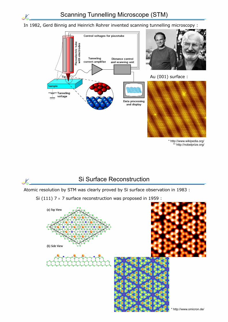
Scanning Tunnelling Microscope (STM)In 1982, Gerd Binnig and Heinrich Rohrer invented scanning tunnelling microscopy :
Au (001) surface :
* http://www.wikipedia.org/** http://nobelprize.org/
tunnelling current
Si Surface ReconstructionAtomic resolution by STM was clearly proved by Si surface observation in 1983 :
* http://www.omicron.de/
Si (111) 7 ´ 7 surface reconstruction was proposed in 1959 :

Si (111) 7 ´ 7 Surface Reconstruction
* http://www.ss.teen.setsunan.ac.jp/2006/si-7x7-das-vr.html
Scanning Tunnelling Spectroscopy (STS) In order to measure a density of states (DOS) with a STM tip,
* http://www.physics.berkeley.edu/research/crommie/research_stm.html

Atom ManipulationAn individual atom can be manipulated by a STM tip shown by Donald Eigler in 1989 :
** http://www.physics.berkeley.edu/research/crommie/research_stm.html* http://www.wikipedia.org/
35 Xe atoms
Atom Manipulation by IBM
Atom Manipulation by IBM
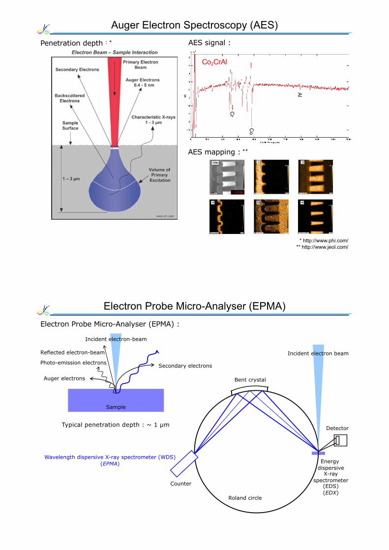
Atomic Force Microscope (AFM)In 1985, Gerd Binnig invented atomic force microscopy :
* http://www.wikipedia.org/
® Non-conductive surface can be observed.

Magnetic Force Microscope (MFM)In 1987, a magnetic tip was introduced to observe a magnetic stray field : *
** http://www.veeco.com/
® By subtracting surface morphology, magnetic domains are observed.
* Y. Martin, H. K. Wickramasinghe, Appl. Phys. Lett. 50, 1455 (1987).
® Similarly, scanning SQUID † / Hall ‡ microscope were developed.† C. C. Tsuei et al., Phys. Rev. Lett. 73, 593 (1994).
‡ A. Oral et al., Appl. Phys. Lett. 69, 1324 (1996).
AFM / MFM OperationDifferent lift height can make a tip to be sensitive to atomic / magnetic forces : *
* A. Hirohata, M. Samiepour, M. Corbetta, "Magnetic Force Microscopy for Magnetic Recording and Devices," in "Electrical Atomic Force Microscopy for Nanoelectronics" Umberto Celano (Ed.) (Springer, Berlin, Germany, 2019) p. 231-265.

AFM / MFM ImagesMFM images can subtract dots morphology :
20 nm thick Fe dots (1 µm diameter) 30 nm thick NiFe dots (5 µm)
Transmission Electron Microscope (TEM)In 1933, Ernst A. F. Ruska and Max Knoll built an electron microscope :
** http://www.wikipedia.org/
• Preliminary electron microscope (´ 17) in 1931
* http://nobelprize.org/
• Improved to ´ 12,000 in 1933
• Sample thickness : 200 ~ 300 nm
• Commercially available from Siemens in 1938
• Magnetic field acts as a lensto electron-beam :
Hans W. H. Busch in 1927

Early TEM ImagesEarly oxide replica of etched Al :
* http://www-g.eng.cam.ac.uk/125/achievements/mcmullan/mcm.htm
Si-Fe :
Scanning Electron Microscope (SEM)In 1937, Manfred von Ardenne developed a scanning electron microscope :
* http://www.wikipedia.org/** http://bluedianni.blogspot.com/2008/05/scanning-electron-microscopy-sem.html

Early SEM ImagesSEM image of etched brass :
* http://www-g.eng.cam.ac.uk/125/achievements/mcmullan/mcm.htm
Scanning Transmission Electron Microscope (STEM)By scanning electron-beam, TEM resolution can be improved significantly :
• 0.8 Å resolution
York JEOL Nanocentre

Capability of STEMBy STEM, H atoms were directly observed :
* S. D. Findlay et al., Appl. Phys. Exp. 3, 116603 (2010).
Annular dark field (ADF) STEM Annular bright field (ABF) STEM
Incident e-beam
Specimen
Diffraction electrons
Detector
Observation of heavy atoms. Observation of heavy andlight atoms at the same time.
Collection of electronswith large scattering angles.
Collection of electronswith small scattering angles.
Surface SpectroscopyBy introducing electron-beam onto a sample surface :
* http://www.wikipedia.org/** http://auger.ung.si/agn/
Auger electrons are found by Lise Meitner in 1922 and Pierre V. Auger in 1925 :
Sample
Secondary electronsPhoto-emission electrons
Incident electron-beam
Reflected electron-beam
Auger electrons
Characteristic X-ray
Auger electrons(AES)
Auger Electron Spectroscopy (AES)Penetration depth : *
** http://www.jeol.com/* http://www.phi.com/
Co2CrAl
Co
Cr
Al
AES signal :
AES mapping : **
Electron Probe Micro-Analyser (EPMA)Electron Probe Micro-Analyser (EPMA) :
Sample
Secondary electronsPhoto-emission electrons
Typical penetration depth : ~ 1 µm
Incident electron-beam
Reflected electron-beam
Auger electrons
Characteristic X-ray(EPMA, EDX)
Detector
Counter
Bent crystal
Roland circle
Wavelength dispersive X-ray spectrometer (WDS)(EPMA) Energy
dispersiveX-ray
spectrometer(EDS)(EDX)
Incident electron beam

EPMA SignalsExample of Co2TiSn :
Shadow edge
0010
01
10
11 11
Laue spots
Surface Structural AnalysisReflection high energy electron diffraction (RHEED) :
Screen
SampleShadow edge Incident electron beam
Direct spot
00 Reflected beam
Typical penetration depth : a few nm01 Reflected beam
[110]
[110]
[010]
Real space : fcc (001) surface
Unit cell
[110]
[110]
Reciprocal lattice : bcc (001)
01
00
11
10
02 12
11
10
12
0th
1st
2nd
Clean surface :
Streak patterns

(2´4) GaAs (001)
[110]
1.0 nm
Co2FeAl
epitaxial L21(clean surface)
2.0 nm
7.5 nm
20 nm
Co2FeAl (001) <110> || GaAs (001) <110>
[110]
[1-10][100]
top view (001)
side view [110]
AsGa 1
Ö 2
bcc [110] ® B2
1Ö 2
bcc [110] ® L21
Zinc blendea = 0.56533 nma
c (2´4) unit mesh
CoCr or Fe Al
RHEED ObservationRHEED patterns of Co2FeAl grown on GaAs (001) :
Surface AnalysisMajor techniques for surface analysis :
* D. P. Woodruff and T. A. Delchar, Modern Techniques of Surface Science (Cambridge University Press, Cambridge, 1994).
Techniques Incident beam Signals Composition Structure Electronic state
Auger electron spectroscopy (AES)
Electron-beam Auger electrons Qualitative analysis Auger electron
spectra
Auger electron diffraction (AED)
Electron-beam Auger electrons Auger diffraction
(~ a few atoms)
Electron probe micro-analyzer (EPMA)
Electron-beam
Characteristic X-ray
Qualitative analysis (sensitivity ~ 0.1 %) X-ray spectra
Energy dispersive X-ray analysis (EDX)
Electron-beam
Characteristic X-ray Qualitative analysis X-ray spectra
X-ray photoelectron spectroscopy (XPS)
Electron-beam
Photo-emission electrons Qualitative analysis Atomic binding
energy
Photoemission electron microscopy (PEEM)
X-ray / photon
Photo-emission electrons Atom mapping Atomic binding
energy
Secondary ion mass spectroscopy (SIMS)
Electron-beam
Secondary electrons Qualitative analysis
Electron energy-lossspectroscopy (EELS)
Electron-beam
Secondary electrons
Surface absorption spectra
Reflection high energy diffraction (RHEED)
Electron-beam
Reflected electron-beam
Reflected diffraction patterns
Low energy electron diffraction (LEED)
Electron-beam
Reflected electron-beam
Back-scattered diffraction patterns
X-ray absorption fine structure (XAFS) X-ray Photo-emission
electronsSurface absorption
spectra
X-ray diffraction (XRD) X-ray Reflected X-ray X-ray diffraction
Transmission electron diffraction (TED)
Electron-beam
Transmission electrons
Diffraction patterns (t < 30 nm)

Detection Limits of Surface Analysis
* http://www.nanoscience.co.jp/surface_analysis/technique/RBS-HFS-PIXE-NRA.html