Nanoelectronic Design Based on a CNT Nano …cdn.intechweb.org/pdfs/9460.pdf˘ˇˆ 0 Nanoelectronic...
36
0 Nanoelectronic Design Based on a CNT Nano-Architecture Bao Liu Electrical and Computer Engineering Department The University of Texas at San Antonio San Antonio, TX, 78249-0669 Email: [email protected] Abstract — Carbon nanotubes (CNTs) and carbon nanotube field effect transistors (CNFETs) have demonstrated extraordinary properties and are widely expected to be the building blocks of next generation VLSI circuits. This chapter presents (1) the first purely CNT and CNFET based nano- architecture, (2) an adaptive configuration methodology for nanoelectronic design based on the CNT nano-architecture, and (3) robust differential asynchronous circuits as a promising nano-circuit paradigm. 1. Introduction Silicon based CMOS technology scaling has driven the semiconductor industry towards cost minimization and performance improvement in the past five decades, and is rapidly ap- proaching its end (30). On the other hand, nanotechnology has achieved significant progress in recent years, fabricating a variety of nanometer scale devices, e.g., molecular diodes (44) and carbon nanotube field effect transistors (CNFETs) (46). This provides new opportunities for VLSI circuits to achieve continuing cost minimization and performance improvement in a post-silicon-based-CMOS-technology era. However, we must overcome a number of significant challenges for practical nanoelectronic systems, including achieving some of the most critical nanoelectronic design metrics as follow. 1. Manufacturability. As minimum layout feature size becomes smaller than lithography light wavelength, traditional lithography based manufacturing process can no longer achieve satisfiable resolution, and leads to significant process variations. Resolution enhancement and other design for manufacturability techniques become less applica- ble as scaling continues. Alternatively, nanoelectronic systems are expected to be based on bottom-up self-assembly based manufacturing processes, e.g., molecular beam epi- taxy (MBE). Such bottom-up self-assembly manufacturing processes provide regular structures, e.g., perfectly aligned carbon nanotubes (23). Consequently, nanoelectronic systems need to rely on reconfigurability to achieve functionality and reliability (51). 2. Reliability. Technology scaling has led to increasingly significant process and system runtime variations, including critical dimension variation, dopant fluctuation, electro- magnetic emission, alpha particle radiation and cosmos ray strikes. Such variations can- not be avoided by manufacturing process improvement, and is inherent at nanometer www.intechopen.com
Transcript of Nanoelectronic Design Based on a CNT Nano …cdn.intechweb.org/pdfs/9460.pdf˘ˇˆ 0 Nanoelectronic...
������������� ���������������������������������� ���
0
Nanoelectronic Design Based on
a CNT Nano-Architecture
Bao LiuElectrical and Computer Engineering Department
The University of Texas at San AntonioSan Antonio, TX, 78249-0669
Email: [email protected]
Abstract — Carbon nanotubes (CNTs) and carbon nanotube field effect transistors (CNFETs) have
demonstrated extraordinary properties and are widely expected to be the building blocks of next
generation VLSI circuits. This chapter presents (1) the first purely CNT and CNFET based nano-
architecture, (2) an adaptive configuration methodology for nanoelectronic design based on the
CNT nano-architecture, and (3) robust differential asynchronous circuits as a promising nano-circuit
paradigm.
1. Introduction
Silicon based CMOS technology scaling has driven the semiconductor industry towards costminimization and performance improvement in the past five decades, and is rapidly ap-proaching its end (30). On the other hand, nanotechnology has achieved significant progressin recent years, fabricating a variety of nanometer scale devices, e.g., molecular diodes (44)and carbon nanotube field effect transistors (CNFETs) (46). This provides new opportunitiesfor VLSI circuits to achieve continuing cost minimization and performance improvement in apost-silicon-based-CMOS-technology era.However, we must overcome a number of significant challenges for practical nanoelectronicsystems, including achieving some of the most critical nanoelectronic design metrics as follow.
1. Manufacturability. As minimum layout feature size becomes smaller than lithographylight wavelength, traditional lithography based manufacturing process can no longerachieve satisfiable resolution, and leads to significant process variations. Resolutionenhancement and other design for manufacturability techniques become less applica-ble as scaling continues. Alternatively, nanoelectronic systems are expected to be basedon bottom-up self-assembly based manufacturing processes, e.g., molecular beam epi-taxy (MBE). Such bottom-up self-assembly manufacturing processes provide regularstructures, e.g., perfectly aligned carbon nanotubes (23). Consequently, nanoelectronicsystems need to rely on reconfigurability to achieve functionality and reliability (51).
2. Reliability. Technology scaling has led to increasingly significant process and systemruntime variations, including critical dimension variation, dopant fluctuation, electro-magnetic emission, alpha particle radiation and cosmos ray strikes. Such variations can-not be avoided by manufacturing process improvement, and is inherent at nanometer
��
www.intechopen.com
�������
�����������
�����������
�����������
�����������
��
��
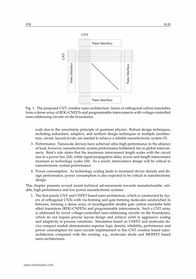
Fig. 1. The proposed CNT crossbar nano-architecture: layers of orthogonal carbon nanotubesform a dense array of RDG-CNFETs and programmable interconnects with voltage-controllednano-addressing circuits on the boundaries.
scale due to the uncertainty principle of quantum physics. Robust design techniques,including redundant, adaptive, and resilient design techniques at multiple (architec-ture, circuit, layout) levels, are needed to achieve a reliable nanoelectronic system (5).
3. Performance. Nanoscale devices have achieved ultra-high performance in the absenceof load, however, nanoelectronic system performance bottleneck lies in global intercon-nects. Rent’s rule states that the maximum interconnect length scales with the circuitsize in a power law (24), while signal propagation delay across unit length interconnectincreases as technology scales (30). As a result, interconnect design will be critical tonanoelectronic system performance.
4. Power consumption. As technology scaling leads to increased device density and de-sign performance, power consumption is also expected to be critical in nanoelectronicdesign.
This chapter presents several recent technical advancements towards manufacturable, reli-able, high performance and low power nanoelectronic systems.
1. The first purely CNT and CNFET based nano-architecture, which is constructed by lay-ers of orthogonal CNTs with via-forming and gate-forming molecules sandwiched inbetween, forming a dense array of reconfigurable double gate carbon nanotube fieldeffect transistors (RDG-CNFETs) and programmable interconnects. Such a CNT arrayis addressed by novel voltage-controlled nano-addressing circuits on the boundaries,which do not require precise layout design and achieve yield in aggressive scalingand adaptivity to process variations. Simulation based on CNFET and molecular de-vice compact models demonstrates superior logic density, reliability, performance andpower consumption for nano-circuits implemented in this CNT crossbar based nano-architecture compared with the existing, e.g., molecular diode and MOSFET basednano-architectures.
www.intechopen.com
������������� ���������������������������������� ���
2. A complete set of linear complexity methods for adaptive configuration of nanoelec-tronic systems based on a CNT crossbar based nano-architecture (Fig. 1) (26), including(1) adaptive nano-addressing, (2) RDG-CNFET gate matching, and (3) catastrophic de-fect mapping methods. Compared with the previous nano-architecture defect mappingand adaptive configuration proposals, these methods are complete, specific, determin-istic, of low runtime complexity. These methods demonstrate the promising prospect ofachieving nanoelectronic systems of correct functionality, performance, and reliabilitybased on the CNT crossbar nano-architecture.
3. Robust Differential Asynchronous (RDA) circuits as a promising paradigm for reliable(noise immune and delay insensitive) high performance and low power nano-circuitsbased on the CNT crossbar nano-architecture. Theoretical analysis and SPICE simu-lation based on 22nm CMOS Predictive Technology Models show that RDA circuitsachieve much enhanced reliability in logic correctness in the presence of a single bitsoft error or common multiple bit soft errors, and timing correctness in the presence ofparametric variations given the physical proximity of the circuit components.
The rest of this chapter is organized as follows. Section 2 reviews the existing nanoelectronicdevices, nano-architectures and nano-addressing circuits. Section 3 presents the proposedCNT crossbar based nano-architecture including a novel RDG-CNFET device, a multi-layerCNT crossbar structure, and a voltage-controlled nano-addressing circuit. Section 4 presentsadaptive configuration methods for nanoelectronic systems based on the CNT crossbar nano-architecture. Section 5 presents robust differential asynchronous circuits as a promising nano-circuit paradigm. Section 6 presents simulation results which evaluate the CNT crossbar nano-architecture and robust differential asynchronous nano-circuits. Section 7 concludes this pa-per with a list of nanotechnologies which enable and improve the proposed CNT crossbarbased nano-architecture.
2. Background
2.1 Existing Nanoscale Devices
Carbon nanotube is one of the most promising candidates for interconnect technology atnanometer scale, due to its extraordinary properties in electrical current carrying capabil-ity, thermal conductivity, and mechanical strength. A carbon nanotube is a one-atom-thickgraphene sheet rolled up in a cylinder of a nanometer-order diameter, which is semicon-ductive or metallic depending on its chirality. The cylinder form eliminates boundaries andboundary-induced scattering, yielding electron mean free path on the order of micrometerscompared with few tens of nanometers in copper interconnects (32). This gives extraordinarycurrent carrying capacity, achieving a current density on the order of 109 A/cm2 (56). How-ever, large resistance exists at CNT-metal contacts, reducing the performance advantage ofCNTs over copper interconnects (38).Among various nanotechnology devices, carbon nanotube field effect transistors are the mostpromising candidates to replace the current CMOS field effect transistors as the buildingblocks of nanoelectronic systems. Three kinds of carbon nanotube based field effect transis-tors (CNFETs) have been manufactured: (1) A Schottky barrier based carbon nanotube fieldeffect transistor (SB-CNFET) consists of a metal-nanotube-metal junction, and works on theprinciple of direct tunneling through the Schottky barrier formed by direct contact of metaland semiconducting nanotube. The barrier width is modulated by the gate voltage. This de-vice has the most mature manufacturing technique up to today, while two problems limit its
www.intechopen.com
������
future: (a) The metal-nanotube contact severely limits current. (b) The ambipolar conductionmakes this devices cannot be applied to conventional circuit design methods. (2) A MOSFET-like CNFET is made by doping a continuous nanotube on both sides of the gate, thus formingthe source/drain regions. This is a unipolar device of high on-current. (3) A band-to-bandtunneling carbon nanotube field effect transistor (T-CNFET) is made by doping the sourceand the drain regions into p+ and n+ respectively. This device has low on-current and ultralow off current, making it potential for ultra low power applications. It also has the potentialto achieve ultra fast signal switching with < 60mV/decade subthreshold slope (46).Molecular electronic devices are based on two families of molecules: the catenanes whichconsist of two or more interlocked rings, and the rotaxanes which consist of one or morerings encircling a dumbbell-shaped component. These molecules can be switched betweenstates of different conductivities in a redox (reduction/oxidation) process by applying cur-rents through them, providing reconfigurability for nanoscale devices (44).A variety of reconfigurable nanoscale devices have been proposed. Resonant tunneling diodesbased on redox active molecules are configurable on/off (44). Nanowire field effect transistorswith redox active molecules at gates are of high/low conductance (17). Spin-RAM devices areof high/low conductivity based on the parallel/anti-parallel magnetization configuration ofthe device which is configured by the polarity of the source voltage (40). A double gate Schot-tky barrier CNFET is configurable to be a p-type FET, an n-type FET, or off, by the electricalpotential of the back gate (25). A double gate field effect transistor with the back gate drivenby a three state RTD memory cell is configurable to be a transistor or an interconnect, reducingreconfiguration cost of a gate array (4).
2.2 Existing Nanoelectronic Architectures
At least three categories of nanoelectronic architectures have been proposed. An early nano-electronic architecture NanoFabrics was based on molecular resonant tunneling diodes (RTDs)and negative differential resistors (NDRs) (20). The insightful authors have observed thatpassive device (diode/resistor) based circuits lack signal gain to recover from signal attenua-tion, while combining with CMOS circuits compromises scaling advantages. They proposedlatches based on negative differential resistors (NDRs), which, unfortunately, have becomeobsolete since the publication.The majority of the existing nanoelectronic architectures are based on a hybrid nano-CMOStechnology, with CMOS circuits complementing nano-circuits. In FPNI (50) (CMOL (54)),a nanowire crossbar is placed on top of CMOS logic gates (inverters). The nanowires pro-vide programmable interconnects (and wired-OR logic), while the CMOS gates(inverters)provide logic implementation (signal inversion and gain). Such architectures achieve compro-mised scaling advantage in term of device density. DeHon (11; 13) proposed to combine pro-grammable nanoscale diode logic arrays with fixed simple CMOS circuitry, e.g., of prechargeand evaluation transistors as in domino logic for signal gain. Sequential elements need also tobe implemented as CMOS circuits. However, the optimal size of a combinational logic blockis typically small (e.g., of 30-50 gates), which results in significant CMOS circuitry overheadin such architectures. An exception is memory design, where CMOS technology provides pe-ripheral circuitry such as address decoders and read sensors with moderate overhead, whilenanotechnology provides scaling advantage in memory cells (17; 47; 63).The third category of existing nanoelectronic architectures rely on DNA-guided self-assemblyto form 2-D scuffles for nanotubes (42; 43) or 3-D DNA-rods (14). Such technologies targetapplication in the far future.
www.intechopen.com
������������� ���������������������������������� ��!
������������������������
��������������
�����������
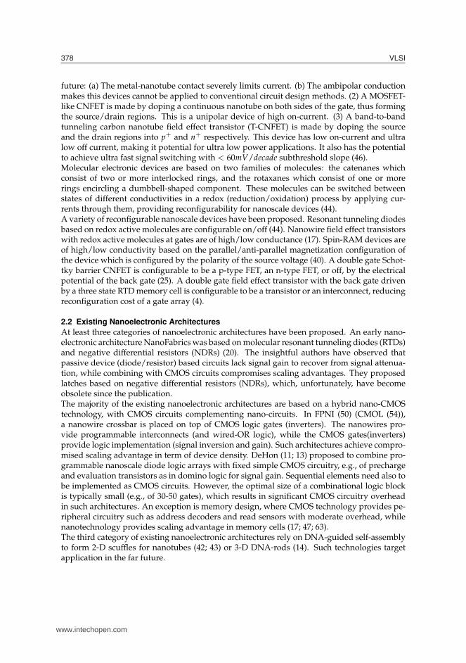
Fig. 2. Layout of undifferentiated nanoscale wires (data lines) addressed by microscale wires(address lines). Lithography defines high- and low-k dielectric regions, which gives field effecttransistors and direct conduction, respectively.
2.3 Existing Nano-Addressing Circuits
A nano-addressing circuit selectively addresses a nanoscale wire in an array, and enables datacommunication between a nano-system and the outside world. The existing nano-addressingcircuits are based on binary decoders, with an array of (microscale) address lines runningacross the (nanoscale) data lines, forming transistors at each crossing (e.g., Fig. 2). Each dataline is selected by a unique binary address, given each data line has a unique gate configura-tion. However, such precise layout design is highly unlikely to achieve at a sublithographicnanometer scale (without significantly compromised yield).In details, the existing nano-addressing circuits are in four categories as follow.
1. Randomized contact decoder (59) includes gold particles which are deposited at ran-dom as contacts between nanoscale and microscale wires. Testing and feedback providea one-to-one mapping between a nanoscale wire and an address.
2. Undifferentiated nanoscale wires are addressable by microscale wires with (e.g., lithog-raphy defined) different gate configurations (which requires nanoscale wire spacing inthe same order of lithography resolution) (22) (Fig. 2).
3. Alternatively, different gate configurations are realized in the nanoscale wires, by grow-ing lightly-doped and heavily-doped carbon nanotubes of different length alternatively,while the microscale wires are undifferentiated. A microscale wire crossing a lightly-doped nanotube segment forms a gate, while a heavily-doped nanotube segment isalways conductive for all possible signals in the microscale wire. In such a case, precisecontrol of the lengths of the lightly- and heavily-doped nanotube segments would becritical (12; 21).
4. In radial addressing, multi-walled carbon nanotubes are grown with lightly- andheavily-doped shells, an etching process removes the heavily-doped outer shells at pre-cise locations, and defines the gate configurations at each crossing of nanoscale andmicroscale wires (48).
www.intechopen.com
����� "
Because process variations are inevitably significant at nanometer scale, these existing nano-addressing structures achieve limited yield, e.g., there is certain probability that two nanoscalewires have identical or similar gate configuration due to process variation. Furthermore,nanoscale wires are mostly partially selected, e.g., they may not achieve the ideal conductivityupon selected, due to process variations such as misalignment, dopant variation, etc.
2.4 Existing Nano-Architecture Defect-Mapping and Adaptive Configuration Methods
Existing nano-architecture defect mapping techniques are as follow. (1) On a Teramac recon-figurable computing platform, signals are propagated along each row or each column in acrossbar structure, a defect is located at the intersection of a defective row and a defective col-umn, based on the assumption that a single defect is present (10). (2) In the NanoFabrics nano-architecture, the roughly estimated number of defects for a subset of computing resources arecollected by counter or none-some-many circuits, a simple graph based algorithm or a Bayes’rule based probabilistic computation procedure gives defect occurrence probability estimates.E.g., highly likely defects are detected in the probability assignment phase, which accumulatesdefect probability in different test configurations, while less likely defects are located in thedefect location phase, which incrementally clears certain spots as non-defects during test ofdifferent configurations (33). (3) A Build-In Self-Test (BIST) method in the NanoFabrics nano-architecture brings much increased complexity with limited applicability (in finding availabledefect-free neighboring nanoBlocks to implement test circuitry) (8; 58).After a defect map is achieved presumably, logic circutis can be constructed avoiding or utiliz-ing the defects. For example, a nanoPLA block can be synthesized in the presence of defectivecrosspoints (36), a CNT nano-circuit layout can be synthesized in the presence of misalignedand mispositioned CNTs (41), metallic CNTs (61), and CNTs of variational density (62).
2.5 Existing CNT Nano-Circuit Design
A very limited number of primitive combinational logic circuits have been fabricated basedon CNFETs, including an inverter and two NOR gates in NMOS logic based on SB-CNFETs(3), and a five-inverter ring oscillator based on MOSFET-like CNFETs (9). While nano-circuitsbased on ambipolar SB-CNFETs need different topologies (3; 46; 53), nano-circuits based onunipolar MOSFET-like CNFETs can be identical to CMOS circuits (9).
3. CNT Crossbar based Nano-Architecture
As we have seen, most existing nanoelectronic architectures are based on diode/resistor logicand CMOS/nano-technologies (11; 13; 20; 50; 54; 63), which only achieve limited manufactura-bility, reliability, and performance. Carbon nanotubes (CNTs) and carbon nanotube field effecttransistors (CNFETs) are the most promising candidates as the the building blocks of nanoelec-tronic systems due to their extraordinary properties. CNTs possess excellent electrical currentcarrying capability, thermal conductivity, and mechanical strength. CNFETs are potential toachieve high on-current, ultra-low off-current, and ultra-fast switching (< 60mV/decade sub-threshold slope). CNT crossbar structure (Fig. 1) is one of the most promising candidatesfor nanoelectronic design platform. Recently, UIUC researchers have achieved fabrication ofdense perfectly aligned CNT arrays (23). Such a CNT crossbar structure forms the basis ofnanoscale memories (17; 47; 63).However, no nanoelectronic architecture has been proposed which is solely based on CNTsand CNFETs. The reasons include lack of (1) a reconfigurable CNT based device which couldprovide functionality and reliability, (2) a self-assembly process which forms complex CNT
www.intechopen.com
������������� ���������������������������������� � #
���� �������
�������
��������
��������������
��
��� ��� �������
��
�������
���!����
"��#�����$
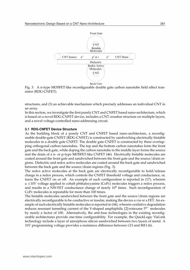
Fig. 3. A n-type MOSFET-like reconfigurable double gate carbon nanotube field effect tran-sistor (RDG-CNFET).
structures, and (3) an achievable mechanism which precisely addresses an individual CNT inan array.In this section, we investigate the first purely CNT and CNFET based nano-architecture, whichis based on a novel RDG-CNFET device, includes a CNT crossbar structure on multiple layers,and a novel voltage-controlled nano-addressing circuit.
3.1 RDG-CNFET Device Structure
As the building block of a purely CNT and CNFET based nano-architecture, a reconfig-urable double-gate CNFET (RDG-CNFET) is constructed by sandwiching electrically bistablemolecules in a double gate CNFET. The double gate CNFET is constructed by three overlap-ping orthogonal carbon nanotubes. The top and the bottom carbon nanotubes form the frontgate and the back gate, while doping the carbon nanotube in the middle layer forms the sourceand the drain of a n- or p-type MOSFET-like CNFET (46). Electrically bistable molecules arecoated around the front gate and sandwiched between the front gate and the source/drain re-gions. Dielectric and redox active molecules are coated around the back gate and sandwichedbetween the back gate and the source/drain regions (Fig. 3).The redox active molecules at the back gate are electrically reconfigurable to hold/releasecharge in a redox process, which controls the CNFET threshold voltage and conductance, or,turns the CNFET on or off. An example of such configuration is reported in (17), whereina ±10V voltage applied to cobalt phthalocyanine (CoPc) molecules triggers a redox process,and results in a NW-FET conductance change of nearly 104 times. Such reconfiguration ofCoPc molecules is repeatable for more than 100 times.The bistable molecules sandwiched between the front gate and the source/drain regions areelectrically reconfigurable to be conductive or insular, making the device a via or a FET. An ex-ample of such electrically bistable molecules is reported in (44), wherein oxidative degradationreduces resonant tunneling current of the V-shaped amphiphilic [2]-rotaxane 54+ moleculesby nearly a factor of 100. Alternatively, the anti-fuse technologies in the existing reconfig-urable architectures provide one-time configurability. For example, the QuickLogic ViaLinktechnology include a layer of amorphous silicon sandwiched between two layers of metal. A10V programming voltage provides a resistance difference between GΩ and 80Ω (6).
www.intechopen.com
����� $
�
�
��
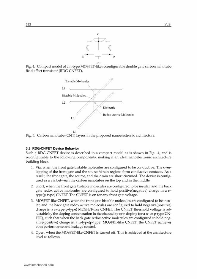
Fig. 4. Compact model of a n-type MOSFET-like reconfigurable double gate carbon nanotubefield effect transistor (RDG-CNFET).
�%
�&
�������
�'
�("��#�����$��������
���������������
���������������
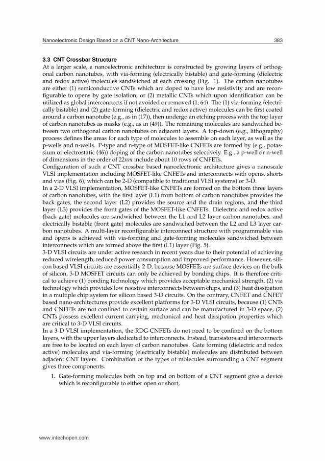
Fig. 5. Carbon nanotube (CNT) layers in the proposed nanoelectronic architecture.
3.2 RDG-CNFET Device Behavior
Such a RDG-CNFET device is described in a compact model as is shown in Fig. 4, and isreconfigurable to the following components, making it an ideal nanoelectronic architecturebuilding block.
1. Via, when the front gate bistable molecules are configured to be conductive. The over-lapping of the front gate and the source/drain regions form conductive contacts. As aresult, the front gate, the source, and the drain are short circuited. The device is config-ured as a via between the carbon nanotubes on the top and in the middle.
2. Short, when the front gate bistable molecules are configured to be insular, and the backgate redox active molecules are configured to hold positive(negative) charge in a n-type(p-type) CNFET. The CNFET is on for any front gate voltage.
3. MOSFET-like CNFET, when the front gate bistable molecules are configured to be insu-lar, and the back gate redox active molecules are configured to hold negative(positive)charge in a n-type(p-type) MOSFET-like CNFET. The CNFET threshold voltage is ad-justable by the doping concentration in the channel (p or n doping for a n- or p-type CN-FET), such that when the back gate redox active molecules are configured to hold neg-ative(positive) charge in a n-type(p-type) MOSFET-like CNFET, the CNFET achievesboth performance and leakage control.
4. Open, when the MOSFET-like CNFET is turned off. This is achieved at the architecturelevel as follows.
www.intechopen.com
������������� ���������������������������������� � �
3.3 CNT Crossbar Structure
At a larger scale, a nanoelectronic architecture is constructed by growing layers of orthog-onal carbon nanotubes, with via-forming (electrically bistable) and gate-forming (dielectricand redox active) molecules sandwiched at each crossing (Fig. 1). The carbon nanotubesare either (1) semiconductive CNTs which are doped to have low resistivity and are recon-figurable to opens by gate isolation, or (2) metallic CNTs which upon identification can beutilized as global interconnects if not avoided or removed (1; 64). The (1) via-forming (electri-cally bistable) and (2) gate-forming (dielectric and redox active) molecules can be first coatedaround a carbon nanotube (e.g., as in (17)), then undergo an etching process with the top layerof carbon nanotubes as masks (e.g., as in (49)). The remaining molecules are sandwiched be-tween two orthogonal carbon nanotubes on adjacent layers. A top-down (e.g., lithography)process defines the areas for each type of molecules to assemble on each layer, as well as thep-wells and n-wells. P-type and n-type of MOSFET-like CNFETs are formed by (e.g., potas-sium or electrostatic (46)) doping of the carbon nanotubes selectively. E.g., a p-well or n-wellof dimensions in the order of 22nm include about 10 rows of CNFETs.Configuration of such a CNT crossbar based nanoelectronic architecture gives a nanoscaleVLSI implementation including MOSFET-like CNFETs and interconnects with opens, shortsand vias (Fig. 6), which can be 2-D (compatible to traditional VLSI systems) or 3-D.In a 2-D VLSI implementation, MOSFET-like CNFETs are formed on the bottom three layersof carbon nanotubes, with the first layer (L1) from bottom of carbon nanotubes provides theback gates, the second layer (L2) provides the source and the drain regions, and the thirdlayer (L3) provides the front gates of the MOSFET-like CNFETs. Dielectric and redox active(back gate) molecules are sandwiched between the L1 and L2 layer carbon nanotubes, andelectrically bistable (front gate) molecules are sandwiched between the L2 and L3 layer car-bon nanotubes. A multi-layer reconfigurable interconnect structure with programmable viasand opens is achieved with via-forming and gate-forming molecules sandwiched betweeninterconnects which are formed above the first (L1) layer (Fig. 5).3-D VLSI circuits are under active research in recent years due to their potential of achievingreduced wirelength, reduced power consumption and improved performance. However, sili-con based VLSI circuits are essentially 2-D, because MOSFETs are surface devices on the bulkof silicon, 3-D MOSFET circuits can only be achieved by bonding chips. It is therefore criti-cal to achieve (1) bonding technology which provides acceptable mechanical strength, (2) viatechnology which provides low resistive interconnects between chips, and (3) heat dissipationin a multiple chip system for silicon based 3-D circuits. On the contrary, CNFET and CNFETbased nano-architectures provide excellent platforms for 3-D VLSI circuits, because (1) CNTsand CNFETs are not confined to certain surface and can be manufactured in 3-D space, (2)CNTs possess excellent current carrying, mechanical and heat dissipation properties whichare critical to 3-D VLSI circuits.In a 3-D VLSI implementation, the RDG-CNFETs do not need to be confined on the bottomlayers, with the upper layers dedicated to interconnects. Instead, transistors and interconnectsare free to be located on each layer of carbon nanotubes. Gate forming (dielectric and redoxactive) molecules and via-forming (electrically bistable) molecules are distributed betweenadjacent CNT layers. Combination of the types of molecules surrounding a CNT segmentgives three components.
1. Gate-forming molecules both on top and on bottom of a CNT segment give a devicewhich is reconfigurable to either open or short,
www.intechopen.com
����� %
�� � �� �)��
������
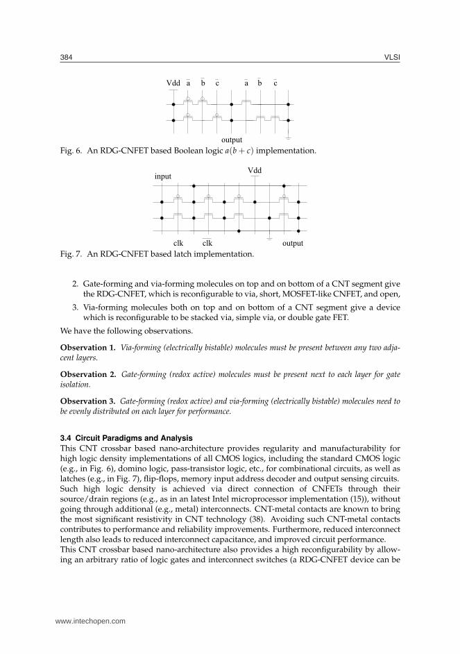
Fig. 6. An RDG-CNFET based Boolean logic a(b + c) implementation.
��������!
)�������
��!
Fig. 7. An RDG-CNFET based latch implementation.
2. Gate-forming and via-forming molecules on top and on bottom of a CNT segment givethe RDG-CNFET, which is reconfigurable to via, short, MOSFET-like CNFET, and open,
3. Via-forming molecules both on top and on bottom of a CNT segment give a devicewhich is reconfigurable to be stacked via, simple via, or double gate FET.
We have the following observations.
Observation 1. Via-forming (electrically bistable) molecules must be present between any two adja-cent layers.
Observation 2. Gate-forming (redox active) molecules must be present next to each layer for gateisolation.
Observation 3. Gate-forming (redox active) and via-forming (electrically bistable) molecules need tobe evenly distributed on each layer for performance.
3.4 Circuit Paradigms and Analysis
This CNT crossbar based nano-architecture provides regularity and manufacturability forhigh logic density implementations of all CMOS logics, including the standard CMOS logic(e.g., in Fig. 6), domino logic, pass-transistor logic, etc., for combinational circuits, as well aslatches (e.g., in Fig. 7), flip-flops, memory input address decoder and output sensing circuits.Such high logic density is achieved via direct connection of CNFETs through theirsource/drain regions (e.g., as in an latest Intel microprocessor implementation (15)), withoutgoing through additional (e.g., metal) interconnects. CNT-metal contacts are known to bringthe most significant resistivity in CNT technology (38). Avoiding such CNT-metal contactscontributes to performance and reliability improvements. Furthermore, reduced interconnectlength also leads to reduced interconnect capacitance, and improved circuit performance.This CNT crossbar based nano-architecture also provides a high reconfigurability by allow-ing an arbitrary ratio of logic gates and interconnect switches (a RDG-CNFET device can be
www.intechopen.com
������������� ���������������������������������� � �
����������'
)���'
����������%
)���%
)���%
)���'
������������������������
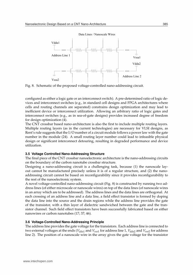
Fig. 8. Schematic of the proposed voltage-controlled nano-addressing circuit.
configured as either a logic gate or an interconnect switch). A pre-determined ratio of logic de-vices and interconnect switches (e.g., in standard cell designs and FPGA architectures wherecells and routing channels are separated) constrains design optimization and may lead toinefficient device or interconnect utilization. Allowing an arbitrary ratio of logic gates andinterconnect switches (e.g., as in sea-of-gate designs) provides increased degree of freedomfor design optimization (4).The CNT crossbar based nano-architecture is also the first to include multiple routing layers.Multiple routing layers (as in the current technologies) are necessary for VLSI designs, asRent’s rule suggests that the I/O number of a circuit module follows a power law with the gatenumber in the module (24). A small routing layer number could lead to infeasible physicaldesign or significant interconnect detouring, resulting in degraded performance and deviceutilization.
3.5 Voltage Controlled Nano-Addressing Structure
The final piece of the CNT crossbar nanoelectronic architecture is the nano-addressing circuitson the boundary of the carbon nanotube crossbar structure.Designing a nano-addressing circuit is a challenging task, because (1) the nanoscale lay-out cannot be manufactured precisely unless it is of a regular structure, and (2) the nano-addressing circuit cannot be based on reconfigurability since it provides reconfigurability tothe rest of the nanoelectronic system.A novel voltage-controlled nano-addressing circuit (Fig. 8) is constructed by running two ad-dress lines (of either microscale or nanoscale wires) on top of the data lines (of nanoscale wiresin an array which are to be addressed). The address lines and the data lines are orthogonal. Ateach crossing of an address line and a data line, a field effect transistor is formed by dopingthe data line into the source and the drain regions while the address line provides the gateof the transistor, with a thin layer of dielectric sandwiched between the gate and the tran-sistor channel. Such field effect transistors have been successfully fabricated based on eithernanowires or carbon nanotubes (17; 37; 46).
3.6 Voltage-Controlled Nano-Addressing Principle
The address line provides the gate voltage for the transistors. Each address line is connected totwo external voltages at the ends (Vdda1 and Vssa1 for address line 1, Vdda2 and Vssa2 for addressline 2). The position of a nanoscale wire in the array gives the gate voltage for the transistor
www.intechopen.com
����� �
on the nanoscale wire alone the address line. For example, a i-th nanoscale wire (starting fromVss) in an array of n equally spaced nanoscale wires has a transistor gate voltage
Vg(i, n) =i
nVdd +
n − i
nVss (1)
in an address line connecting to two external voltage sources Vdd and Vss. Here we assumeuniform address lines of negligible external resistance (from the first or the last nanoscale wireto the nearest external voltage source).A transistor is on if its gate voltage exceeds the threshold voltage Vg > Vth. A nanoscalewire is conductive if both transistors on it are on. Because the two address lines provide anincreasing series and a decreasing series of gate voltages respectively, only nanoscale wires atspecific positions in the array are conductive. For example, for Vdda1 = Vdda2 and Vssa1 = Vssa2,the nanoscale wire in the middle of the array gets conductive.In general, to select the i-th data line from the left in an array of n nanoscale wires, the externalvoltages need to be such that all the transistors on the right hand side of the i-th data line inthe first address line are off, and all the transistors on the left hand side of the i-th data line inthe second address line are off:
Vga1(i + 1, n) = (1 −i + 1
n)Vdda1 +
i + 1n
Vssa1 < Vth
Vga2(i − 1, n) =i − 1
nVdda2 + (1 −
i − 1n
)Vssa2 < Vth (2)
3.7 Voltage Controlled Nano-Addressing Analysis
Compared with the existing nano-addressing circuits, the proposed voltage-controlled nano-addressing circuit leads to significant manufacturing yield improvement due to the followingreasons.The existing nano-addressing circuits are based on binary decoders and require everynanoscale wire have a unique physical structure to differentiate itself, which is highly unlikely ina nanotechnology manufacturing process - lithography cannot achieve nanoscale resolution,while bottom-up self-assembly based nanotechnology manufacturing processes provide onlyregular structures. Even at microscale, such a structure is subject to prevalent catastrophicdefects and significant parametric variations, which result in low yield.On the contrary, the proposed circuit consists of only uniform components in a regular struc-ture. Every nanoscale wire has a uniform physical structure and is differentiated by their electricalparameters, e.g., the node voltages. This scheme avoids any precise layout design and signifi-cantly improves yield and enables aggressive scaling of the addressing circuit with the rest ofthe nanoelectronic system.Furthermore, let us compare voltage-controlled nano-addressing with the existing binary de-coder based nano-addressing mechanisms in terms of addressing accuracy and resolution.These two key quantitative metrics for nano-addressing circuits are defined as follow sincesuch definition is not available in previous publications to the best of the author’s knowledge.
Definition 1. Addressing inaccuracy of a nano-addressing circuit is the offset between the targetdata line i and the data line j of maximum current.
AI = |i − j| (3)
www.intechopen.com
������������� ���������������������������������� � �
In voltage-controlled nano-addressing, addressing inaccuracy is given by inaccurate address-ing voltages from the voltage dividers. Such addressing inaccuracy can be further minimizedby adjusting the external voltages to adapt to manufacturing process and system runtimeparametric variations. As a result, a mis-addressing is localized, i.e., the data line j of maxi-mum current is not far from the target data line i.In traditional binary decoder based nano-addressing, an n-bit binary address has n neigh-boring binary addresses of Hamming distance 1. A 1-bit error could lead to n different mis-addressings. This leads to non-localized mis-addressing and a more significant addressinginaccuracy.
Definition 2. Addressing resolution of a nano-addressing circuit is the minimum ratio between theon current Ion(i) of a target data line i and the off current Io f f (j) of a non-target data line j (under allconditions, e.g., different inputs and parametric variations).
AR = Min{Ion(i)
Io f f (j)} (4)
In traditional binary decoder based nano-addressing, the achievable addressing resolution de-pends on the conductance difference between the target data line and other non-target datalines. There are n non-target data lines with Hamming distance 1 for a n-bit target address,which have similar if not identical conductances. The presence of parametric variations fur-ther reduces addressing resolution.In voltage-controlled nano-addressing, addressing resolution is largely given by the address-ing voltage difference between two adjacent data lines. Applying high voltages leads to anumber of reliability issues, such as electromigration and gate dioxide breakdown. Carbonnanotubes are highly resistive to electromigration, while new material is needed to enhancereliability for gate dioxide breakdown.Alternatively, for given gate voltage difference, transistor current difference can be improvedby improving the inverse subthreshold slope. However, MOSFETs and MOSFET-like CNFETsare limited to an inverse subthreshold slope S (which is the minimum gate voltage variationneeded to bring a 10× source-drain current increase) of 2.3 kT
q ≈ 60mV/decade at 300K (46).This requires development of novel devices for larger inverse subthreshold slopes.
4. Adaptive Configuration of Nanoelectronic Systems Based on the CNT Crossbar
Nano-Architecture
In this section, we examine a list of nanoelectronic design adaptive configuration methodswhich cancel the effects of catastrophic defects and parametric variations in the proposedCNT crossbar nano-architecture.
4.1 Adaptive Nano-Addressing
A variety of parametric variations are expected to be prevalent and significant in nanoelec-tronic systems. Their effects on the voltage-controlled nano-addressing circuit (Fig. 8) are asfollow.
1. Global address line resistance variations, e.g., due to uniform width, height, and/orresistivity variations of the address lines, have no effect on the voltage divider hencethe addressing scheme.
2. Address line misalignment (shifting) has no effect on the conductances of the data lines.
www.intechopen.com
�����
)*
"
"
)�
� �� +
∆ ,���"∆����"
"* �
�"*
Fig. 9. Addressing two CNTs Di and Dj with a resistance of ΔR in between.
3. Global data line misalignment (i.e., shifting of all data lines), variations of external volt-age sources, and variations of external wire/contact resistance (between the resistivevoltage divider and the external voltage sources) lead to potential addressing inaccu-racy (CNT target offset).
4. Individual data line misalignment (shifting) could decrease the difference between thegate voltages of two adjacent transistors, leading to degraded addressing resolution(on/off CNT current ratio between two adjacent CNTs).
5. Process variations of the transistors, including width, length, dopant concentration, andoxide thickness variations, lead to transistor conductivity uncertainty and degradedaddressing resolution.
The nano-addressing scheme needs to achieve a higher enough addressing resolution whichendures the above-mentioned parametric variation effects (e.g., by applying high externaladdressing voltages, and/or novel CNFETs of < 60mV/decade subthreshold slope).After achieving satisfiable addressing resolution, we need to minimize any addressing inac-curacy and address the correct CNT data line (Problem 1).
Problem 1 (Adaptive Nano-Addressing). Given a voltage-controlled nano-addressing circuit, ad-dress the i-th CNT data line in the presence of parametric variations.
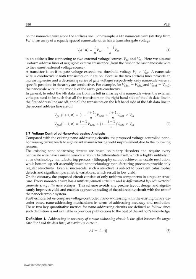
Let us first derive the external voltage offset needed for a data address offset. Suppose for anaddress line, the external voltages Vh and Vl address the i-th CNT data line Di. The resistancebetween CNT data line Di and the high (low) external address voltage Vh (Vl) is Rh (Rl) (Fig.9).1 We have
Rl
Rh + RlVh +
Rh
Rh + RlVl = Von (5)
where Von is the voltage needed to address a CNT data line of peak current. Shifting theexternal voltages to Vh + ΔV and Vl + ΔV addresses another CNT data line Dj. The resistancebetween CNT data line Dj and the high (low) external address voltage is Rh + ΔR (Rl − ΔR).We have
Rl − ΔR
Rh + Rl(Vh + ΔV) +
Rh + ΔR
Rh + Rl(Vl + ΔV) = Von (6)
1 For the first address line, the high external voltage Vh = Vl1 is on the left, the low external voltageVl = Vr1 is on the right. For the second address line, the high external voltage Vh = Vr2 is on the right,the low external voltage Vl = Vl2 is on the left.
www.intechopen.com
������������� ���������������������������������� � !
As a result,
ΔV =ΔR
Rh + Rl(Vh − Vl) (7)
Observation 4. The external voltage offset ΔV is proportional to the resistance offset ΔR between twoCNT data lines, and is proportional to the physical offset ΔL between the two CNT data lines, if theresistive voltage dividers are uniform (e.g., the CNT data lines are equally spaced and the address lineshave uniform resistivity).
Based on Observation 1, Method 1 gives an adaptive nanoelectronic addressing method,which finds the external voltage shifts needed to address the left most and the right mostCNT data lines first. Any other external voltage shift needed to address a specific CNT dataline is then computed based on a linear interpolation. To address the left most or the rightmost CNT data line, we apply a gradually increasing/decreasing external voltage offset ΔVat an address line, keep all the transistors at the other address line on, and measure the con-ductance of the array of CNT data lines. The maximum and the minimum ΔV’s (e.g., ΔVmink
and ΔVmaxk, k = 1 or 2) with non-zero CNT data line conductances address the left most andthe right most CNT data lines, respectively.
Algorithm 1: Adaptive Voltage ControlledNano Addressing
Input: An array of n CNT data lines, address iOutput: Addressing i-th data line
1. Turn on all transistors at address line 2 (Vl2 =Vr2 > Vth)2. Find ΔVl1 which addresses first data line (bi-nary search)3. Find ΔVr1 which addresses n-th data line (bi-nary search)4. Turn on all transistors at address line 1 (Vl1 =Vr1 > Vth)5. Find ΔVl2 which addresses first data line (bi-nary search)6. Find ΔVr2 which addresses n-th data line (bi-nary search)7. Shift Vl1 and Vr1 by n−i
n ΔVl1 +in ΔVr1
8. Shift Vl2 and Vr2 by n−in ΔVl2 +
in ΔVr2
Observation 5. The addressing accuracy given by Method 1 depends only on the uniformity of theresistive voltage divider, and the time domain variations of the external voltage differences Vl1 − Vr1and Vl2 − Vr2. Any time-invariant (e.g., manufacturing process) variations of the external voltages(Vl1, Vr1, Vl2, and Vr2) or the external address line resistances (from the outer most data lines to theexternal voltage sources) do not affect the achievable addressing accuracy.
4.2 RDG-CNFET Gate Matching
Another process variation is the misalignment of the front gate CNT and the back gate CNT ofa reconfigurable double-gate CNFET (RDG-CNFET). This is because that the front gate CNTand the back gate CNT are on different (i − 1 and i + 1) layers, while CNT arrays on differentlayers do not have and are not expected to have a precise alignment mechanism.
www.intechopen.com
�����!"
��������
��������������
��
�� ������� �� �������
��
�������
���!����
"��#�����$
��
�������
���!����
"��#�����$
��������
��������������
��
��
�������
���!����
"��#�����$
��
�������
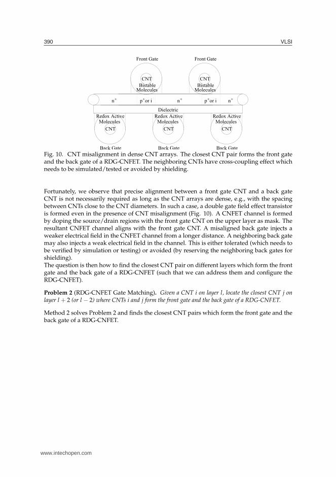
Fig. 10. CNT misalignment in dense CNT arrays. The closest CNT pair forms the front gateand the back gate of a RDG-CNFET. The neighboring CNTs have cross-coupling effect whichneeds to be simulated/tested or avoided by shielding.
Fortunately, we observe that precise alignment between a front gate CNT and a back gateCNT is not necessarily required as long as the CNT arrays are dense, e.g., with the spacingbetween CNTs close to the CNT diameters. In such a case, a double gate field effect transistoris formed even in the presence of CNT misalignment (Fig. 10). A CNFET channel is formedby doping the source/drain regions with the front gate CNT on the upper layer as mask. Theresultant CNFET channel aligns with the front gate CNT. A misaligned back gate injects aweaker electrical field in the CNFET channel from a longer distance. A neighboring back gatemay also injects a weak electrical field in the channel. This is either tolerated (which needs tobe verified by simulation or testing) or avoided (by reserving the neighboring back gates forshielding).The question is then how to find the closest CNT pair on different layers which form the frontgate and the back gate of a RDG-CNFET (such that we can address them and configure theRDG-CNFET).
Problem 2 (RDG-CNFET Gate Matching). Given a CNT i on layer l, locate the closest CNT j onlayer l + 2 (or l − 2) where CNTs i and j form the front gate and the back gate of a RDG-CNFET.
Method 2 solves Problem 2 and finds the closest CNT pairs which form the front gate and theback gate of a RDG-CNFET.
www.intechopen.com
������������� ���������������������������������� �!#
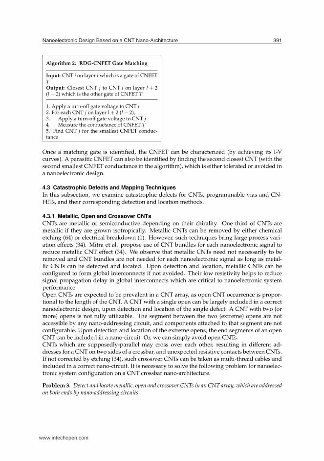
Algorithm 2: RDG-CNFET Gate Matching
Input: CNT i on layer l which is a gate of CNFETTOutput: Closest CNT j to CNT i on layer l + 2(l − 2) which is the other gate of CNFET T
1. Apply a turn-off gate voltage to CNT i2. For each CNT j on layer l + 2 (l − 2),3. Apply a turn-off gate voltage to CNT j4. Measure the conductance of CNFET T5. Find CNT j for the smallest CNFET conduc-tance
Once a matching gate is identified, the CNFET can be characterized (by achieving its I-Vcurves). A parasitic CNFET can also be identified by finding the second closest CNT (with thesecond smallest CNFET conductance in the algorithm), which is either tolerated or avoided ina nanoelectronic design.
4.3 Catastrophic Defects and Mapping Techniques
In this subsection, we examine catastrophic defects for CNTs, programmable vias and CN-FETs, and their corresponding detection and location methods.
4.3.1 Metallic, Open and Crossover CNTs
CNTs are metallic or semiconductive depending on their chirality. One third of CNTs aremetallic if they are grown isotropically. Metallic CNTs can be removed by either chemicaletching (64) or electrical breakdown (1). However, such techniques bring large process vari-ation effects (34). Mitra et al. propose use of CNT bundles for each nanoelectronic signal toreduce metallic CNT effect (34). We observe that metallic CNTs need not necessarily to beremoved and CNT bundles are not needed for each nanoelectronic signal as long as metal-lic CNTs can be detected and located. Upon detection and location, metallic CNTs can beconfigured to form global interconnects if not avoided. Their low resistivity helps to reducesignal propagation delay in global interconnects which are critical to nanoelectronic systemperformance.Open CNTs are expected to be prevalent in a CNT array, as open CNT occurrence is propor-tional to the length of the CNT. A CNT with a single open can be largely included in a correctnanoelectronic design, upon detection and location of the single defect. A CNT with two (ormore) opens is not fully utilizable. The segment between the two (extreme) opens are notaccessible by any nano-addressing circuit, and components attached to that segment are notconfigurable. Upon detection and location of the extreme opens, the end segments of an openCNT can be included in a nano-circuit. Or, we can simply avoid open CNTs.CNTs which are supposedly-parallel may cross over each other, resulting in different ad-dresses for a CNT on two sides of a crossbar, and unexpected resistive contacts between CNTs.If not corrected by etching (34), such crossover CNTs can be taken as multi-thread cables andincluded in a correct nano-circuit. It is necessary to solve the following problem for nanoelec-tronic system configuration on a CNT crossbar nano-architecture.
Problem 3. Detect and locate metallic, open and crossover CNTs in an CNT array, which are addressedon both ends by nano-addressing circuits.
www.intechopen.com
�����!$
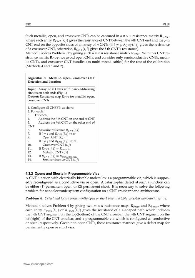
Such metallic, open, and crossover CNTs can be captured in a n × n resistance matrix RCNT ,where each entry RCNT(i, j) gives the resistance of CNT between the i-th CNT end and the j-thCNT end on the opposite sides of an array of n CNTs (if i �= j, RCNT(i, j) gives the resistanceof a crossover CNT, otherwise, RCNT(i, i) gives the i-th CNT’s resistance).Method 3 solves Problem 3 by giving such a n × n resistance matrix RCNT . With this CNT re-sistance matrix RCNT , we avoid open CNTs, and consider only semiconductive CNTs, metal-lic CNTs, and crossover CNT bundles (as multi-thread cables) for the rest of the calibration(Methods 4 and 5 and 2).
Algorithm 3: Metallic, Open, Crossover CNTDetection and Location
Input: Array of n CNTs with nano-addressingcircuits on both ends (Fig. 1)Output: Resistance map RCNT for metallic, open,crossover CNTs
1. Configure all CNFETs as shorts2. For each i3. For each j4. Address the i-th CNT on one end of CNT5. Address the j-th CNT on the other end ofCNT6. Measure resistance RCNT(i, j)7. If i = j and RCNT(i, j) ≈ ∞
8. Open CNT (i, j)9. If i �= j and RCNT(i, j) ≪ ∞
10. Crossover CNT (i, j)11. If RCNT(i, j) ≈ Rmetallic
12. Metallic CNT (i, j)13. If RCNT(i, j) ≈ Rsemiconductive
14. Semiconductive CNT (i, j)
4.3.2 Opens and Shorts in Programmable Vias
A CNT junction with electrically bistable molecules is a programmable via, which is suppos-edly reconfigured as a conductive via or open. A catastrophic defect at such a junction canbe either (1) permanent open, or (2) permanent short. It is necessary to solve the followingproblem for nanoelectronic system configuration on a CNT crossbar nano-architecture.
Problem 4. Detect and locate permanently open or short vias in a CNT crossbar nano-architecture.
Method 4 solves Problem 4 by giving two m × n resistance maps RPmin and RPmax, whereeach entry RPmin(i, j) or RPmax(i, j) gives the resistance of a L-shaped path which includesthe i-th CNT segment on the top(bottom) of the CNT crossbar, the j-th CNT segment on theleft(right) of the CNT crossbar, and a programmable via which is configured as conductiveor open, respectively. Given non-open CNTs, these resistance matrices give a defect map forpermanently open or short vias.
www.intechopen.com
������������� ���������������������������������� �!�
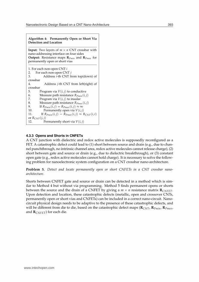
Algorithm 4: Permanently Open or Short ViaDetection and Location
Input: Two layers of m × n CNT crossbar withnano-addressing interface on four sidesOutput: Resistance maps RPmin and RPmax forpermanently open or short vias
1. For each non-open CNT i2. For each non-open CNT j3. Address i-th CNT from top(down) ofcrossbar4. Address j-th CNT from left(right) ofcrossbar5. Program via V(i, j) to conductive6. Measure path resistance RPmin(i, j)7. Program via V(i, j) to insular8. Measure path resistance RPmax(i, j)9. If RPmin(i, j) = RPmax(i, j) ≈ ∞
10. Permanently open via V(i, j)11. If RPmin(i, j) = RPmax(i, j) ≈ RCNT(i, i)or RCNT(j, j)12. Permanently short via V(i, j)
4.3.3 Opens and Shorts in CNFETs
A CNT junction with dielectric and redox active molecules is supposedly reconfigured as aFET. A catastrophic defect could lead to (1) short between source and drain (e.g., due to chan-nel punchthrough, no intrinsic channel area, redox active molecules cannot release charge), (2)short between gate and source or drain (e.g., due to dielectric breakthrough), or (3) constantopen gate (e.g., redox active molecules cannot hold charge). It is necessary to solve the follow-ing problem for nanoelectronic system configuration on a CNT crossbar nano-architecture.
Problem 5. Detect and locate permanently open or short CNFETs in a CNT crossbar nano-architecture.
Shorts between CNFET gate and source or drain can be detected in a method which is sim-ilar to Method 4 but without via programming. Method 5 finds permanent opens or shortsbetween the source and the drain of a CNFET by giving a m × n resistance matrix RCNFET .Upon detection and location, these catastrophic defects (metallic, open and crossover CNTs,permanently open or short vias and CNFETs) can be included in a correct nano-circuit. Nano-circuit physical design needs to be adaptive to the presence of these catastrophic defects, andwill be different from die to die, based on the catastrophic defect maps (RCNT , RPmin, RPmax,and RCNFET) for each die.
www.intechopen.com
�����!%
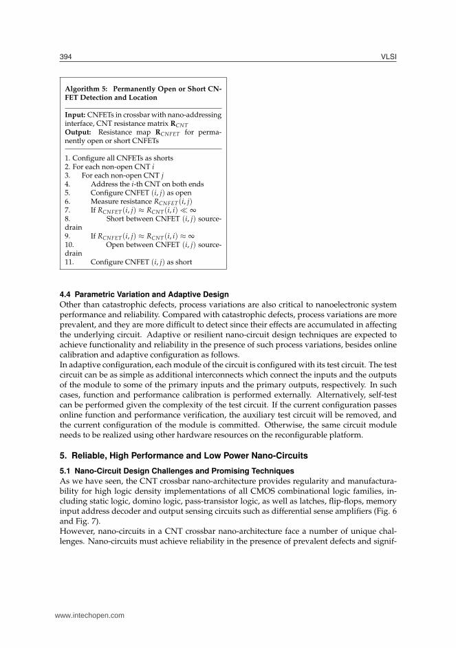
Algorithm 5: Permanently Open or Short CN-FET Detection and Location
Input: CNFETs in crossbar with nano-addressinginterface, CNT resistance matrix RCNT
Output: Resistance map RCNFET for perma-nently open or short CNFETs
1. Configure all CNFETs as shorts2. For each non-open CNT i3. For each non-open CNT j4. Address the i-th CNT on both ends5. Configure CNFET (i, j) as open6. Measure resistance RCNFET(i, j)7. If RCNFET(i, j) ≈ RCNT(i, i) ≪ ∞
8. Short between CNFET (i, j) source-drain9. If RCNFET(i, j) ≈ RCNT(i, i) ≈ ∞
10. Open between CNFET (i, j) source-drain11. Configure CNFET (i, j) as short
4.4 Parametric Variation and Adaptive Design
Other than catastrophic defects, process variations are also critical to nanoelectronic systemperformance and reliability. Compared with catastrophic defects, process variations are moreprevalent, and they are more difficult to detect since their effects are accumulated in affectingthe underlying circuit. Adaptive or resilient nano-circuit design techniques are expected toachieve functionality and reliability in the presence of such process variations, besides onlinecalibration and adaptive configuration as follows.In adaptive configuration, each module of the circuit is configured with its test circuit. The testcircuit can be as simple as additional interconnects which connect the inputs and the outputsof the module to some of the primary inputs and the primary outputs, respectively. In suchcases, function and performance calibration is performed externally. Alternatively, self-testcan be performed given the complexity of the test circuit. If the current configuration passesonline function and performance verification, the auxiliary test circuit will be removed, andthe current configuration of the module is committed. Otherwise, the same circuit moduleneeds to be realized using other hardware resources on the reconfigurable platform.
5. Reliable, High Performance and Low Power Nano-Circuits
5.1 Nano-Circuit Design Challenges and Promising Techniques
As we have seen, the CNT crossbar nano-architecture provides regularity and manufactura-bility for high logic density implementations of all CMOS combinational logic families, in-cluding static logic, domino logic, pass-transistor logic, as well as latches, flip-flops, memoryinput address decoder and output sensing circuits such as differential sense amplifiers (Fig. 6and Fig. 7).However, nano-circuits in a CNT crossbar nano-architecture face a number of unique chal-lenges. Nano-circuits must achieve reliability in the presence of prevalent defects and signif-
www.intechopen.com
������������� ���������������������������������� �!�
icant parametric variations, must achieve performance with highly resistive CNT intercon-nects, etc. We discuss nano-circuit design in a CNT crossbar nano-architecture in this section.Nanoscale computing systems are expected to be subject to prevalent defects and significantprocess and environmental variations inevitably as a result of the uncertainty principle ofquantum physics. E.g., the conductance of a CNT or a CNFET is very sensitive to chirality,diameter, etc. (38). Besides adaptive configuration, nanoscale computing systems need newcomputing models or circuit paradigms for reliability enhancement, performance improve-ment and power consumption reduction.As technology scales, nanoelectronic computing systems are expected to be based on singleelectron devices (the average number of electrons in a transistor channel is approaching onefor the current technologies). In quantum mechanics, the occurrence probability of an electronis the wavefunction given by the Schrodinger equation. How to extract a deterministic com-putation result from stochastic events such as electron occurrences is one of the fundamentalproblems that we are facing in designing nanometer scale computing systems. Traditionalcomputation based on large devices can be modeled as redundancy and threshold based logic(which includes majority logic). In redundancy and threshold based logic, the error rate isgiven by a binomial distribution (the probability of observing m events in an environment ofexpecting an average of n independent events). As a result, a minimum signal-to-noise ratiois required with performance and power consumption implications. Finding a more efficientreliable computing model is of essential interest in nanoelectronic design.Besides stochastic signal occurrence, signal propagation delay variability is another categoryof uncertainty in stochastic nanoscale systems. Nanoelectronic design needs to be adaptive toor resilient in the presence of signal propagation delay variations. Existing techniques (e.g.,the Razor technology (2; 18) wherein a shadow flip-flop captures a delayed data signal for tim-ing verification and correction) achieves only limited performance adaptivity, e.g., the circuityis adaptive to performance variations only within a given range. Asynchronous circuits haveunlimited adaptivity to performance variations, and are ideal for high performance (enablingperformance scaling in the presence of significant performance variations) and low power (be-ing event-driven and clockless) nanoelectronic design (e.g., multi-core chips are expected to beincreasingly self-timed, global-asynchronous-locally-synchronous, or totally asynchronous).However, existing asynchronous design techniques suffer in reliability in the presence of softerrors (e.g., glitches, coupling noises, radiation or cosmos ray strike induced random noises),which has limited their applications for decades.A number of robust design techniques at multiple levels help to enhance reliability and reduceerror rate of a nanoelectronic computing system. At the circuit level, differential signaling andcomplementary logic reduces parametric variation effects by exploiting spatial and temporalcorrelations (e.g., by correlating m and n for reduced error rate in a binomial distribution) (15;31; 57). At a higher level, we believe that Error Detection/Correction Code (35) is the key tothe stochastic signal occurrence problem in nanoscale systems (e.g., for lower required signal-to-noise ratios, which lead to high performance and low power), and needs to be applied moreextensively at a variety of design hierarchy levels. Error correction coding has been appliedwidely in today’s memories and wireless communication systems. Proposals also exist forapplying (AN or residue) error detection/correction coding in arithmetic circuits (7).
www.intechopen.com
�����!�
�
�$����
$����-�.
$����-�.�/�
�/�
�/�
�/�
0
��!/�
��!/�
��!/�
��!/�
$����
�
�
�������
�������
��
$����-�.
$����-�.
�/�
�/�
�!/��!/�
�/��/�
%
��!/��
%
��!/��
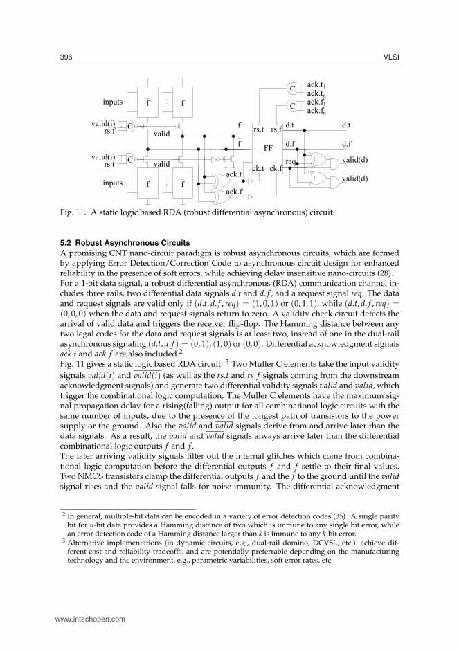
Fig. 11. A static logic based RDA (robust differential asynchronous) circuit.
5.2 Robust Asynchronous Circuits
A promising CNT nano-circuit paradigm is robust asynchronous circuits, which are formedby applying Error Detection/Correction Code to asynchronous circuit design for enhancedreliability in the presence of soft errors, while achieving delay insensitive nano-circuits (28).For a 1-bit data signal, a robust differential asynchronous (RDA) communication channel in-cludes three rails, two differential data signals d.t and d. f , and a request signal req. The dataand request signals are valid only if (d.t, d. f , req) = (1, 0, 1) or (0, 1, 1), while (d.t, d. f , req) =(0, 0, 0) when the data and request signals return to zero. A validity check circuit detects thearrival of valid data and triggers the receiver flip-flop. The Hamming distance between anytwo legal codes for the data and request signals is at least two, instead of one in the dual-railasynchronous signaling (d.t, d. f ) = (0, 1), (1, 0) or (0, 0). Differential acknowledgment signalsack.t and ack. f are also included.2
Fig. 11 gives a static logic based RDA circuit. 3 Two Muller C elements take the input validitysignals valid(i) and valid(i) (as well as the rs.t and rs. f signals coming from the downstreamacknowledgment signals) and generate two differential validity signals valid and valid, whichtrigger the combinational logic computation. The Muller C elements have the maximum sig-nal propagation delay for a rising(falling) output for all combinational logic circuits with thesame number of inputs, due to the presence of the longest path of transistors to the powersupply or the ground. Also the valid and valid signals derive from and arrive later than thedata signals. As a result, the valid and valid signals always arrive later than the differentialcombinational logic outputs f and f .The later arriving validity signals filter out the internal glitches which come from combina-tional logic computation before the differential outputs f and f settle to their final values.Two NMOS transistors clamp the differential outputs f and the f to the ground until the validsignal rises and the valid signal falls for noise immunity. The differential acknowledgment
2 In general, multiple-bit data can be encoded in a variety of error detection codes (35). A single paritybit for n-bit data provides a Hamming distance of two which is immune to any single bit error, whilean error detection code of a Hamming distance larger than k is immune to any k-bit error.
3 Alternative implementations (in dynamic circuits, e.g., dual-rail domino, DCVSL, etc.) achieve dif-ferent cost and reliability tradeoffs, and are potentially preferrable depending on the manufacturingtechnology and the environment, e.g., parametric variabilities, soft error rates, etc.
www.intechopen.com
������������� ���������������������������������� �!�
signals ack.t and ack. f derive from and always appear later than the differential data signalsf and f .At the sender’s end of the interconnect, for sequential elements, flip-flops are preferred overlatches for reliability. A flip-flop is only vulnerable to noise when capturing the signal, while alatch is vulnerable to noise whenever it is transparent. The flip-flops send out differential datasignals d.t and d. f (which come from the differential combinational logic outputs f and f ) aswell as a request req signal (which comes from the acknowledgment signal ack.t). At the re-ceiver end of the interconnect, a group of XOR and AND(NAND) gates verify the differentialdata and request signals, and generate two differential validity signals valid(d) and valid(d).Any single bit soft error or common multiple bit soft errors injected to the interconnects or atthe validity signals will halt the circuit.Each sender flip-flop is triggered by two differential acknowledgment signals ack.t and ack. fas the differential clock signals ck.t = 1 and ck. f = 0, and is reset by two differential resetsignals when rs.t = 1 and rs. f = 0. The differential reset signals come from the downstreamdifferential acknowledgment signals ack.ti and ack. fi via the Muller C elements. They alsogenerate the valid and valid signals which trigger the combinational logic computation.In the presence of multiple fanouts, multiple sets of differential acknowledgment signals willbe sent back to the upstream stage. With the Muller C elements holding the input validity sig-nals, the early arriving acknowledgment signals hold until the latest acknowledgment signalarrive from the fanouts. At that time the Muller C elements close the inputs to the combina-tional logic block and reset the flip-flop at the upstream stage, which brings all differentialdata and request signals d.t, d. f and req as well as the acknowledgment signals ack.t and ack. fback to the ground, completing an asynchronous communication cycle.
5.3 Logic and Timing Correctness of RDA Circuits
An RDA circuit achieves logic and timing correctness in the presence of a single bit soft erroror common multiple bit soft errors given the physical proximity of the circuit components.
Definition 3 (Single Bit Soft Error). A single bit soft error is a glitch or toggling caused by a singleevent upset as a result of an alpha particle or neutron strike from radioactive material or cosmos rays.
Definition 4 (Common Multiple Bit Soft Error). A common multiple bit soft error is glitches ortogglings of the same magnitude and polarity caused by common noises such as capacitive or inductiveinterconnect coupling, or spatially correlated transient parametric (e.g., supply voltage, temperature)variations (19; 39; 60), which have near identical effects on components at close physical proximity.
Theorem 1 (Logic Correctness). An robust differential asynchronous circuit achieves logic correct-ness at the event of a single bit soft error or common multiple bit soft errors.
Proof. An RDA circuit achieves logic correctness in the following cases.
1. A single bit soft error or a common multiple bit soft error at the input data signals leadsto invalid data. The valid(i)(valid(i)) signal will not rise(fall).
2. A single bit soft error or a common multiple bit soft error at the valid(i) and valid(i)signals, at the Muller C elements computing the valid and valid signals, or at the validand valid signals, leads to an early false or a late valid(valid) signal. In this case, thedifferential structure for the valid/valid signals prevents any logic error. A false validsignal turns off the keeper circuit, but can rise neither f nor f , because the valid signalis still high. A false valid signal rises either f or f , while the keeper circuit still clamps
www.intechopen.com
�����!
both f and f to the ground. Only when both the valid and valid signals arrive, thedifferential combinational logic computation is enabled.
3. A single bit soft error or a common multiple bit soft error at the differential combina-tional logic block or the differential data signals f and f will not raise the ack.t signalnor lower the ack. f signal.4
4. A single bit soft error or a common multiple bit soft error at the differential acknowl-edgment signals ack.t and ack. f does not trigger the flip-flop.
5. A single bit soft error or a common multiple bit soft error at the differential reset signalsRS and RS does not reset the flip-flop.
6. A single bit soft error or a common multiple bit soft error at the differential data signalsd.t and d. f and the request req signal leads to invalid data and does not generate avalidity signal.
In summary, in order to make an RDA circuit to fail, the glitches must follow certain specificpatterns, e.g., to reverse a “01” to a “10”, which is highly unlikely to take place.
⊓⊔
Theorem 2 (Timing Correctness). An robust differential asynchronous circuit achieves timing cor-rectness for any delay variation given the physical proximity of the circuit components.
Proof. Prevalent parametric (process, temperature, supply voltage) variations in nanoelec-tronic circuits lead to significant delay variations for the components in the circuit. Becausesuch delay variations are spatially correlated (19; 39; 60), given the physical proximity of thecircuit components, their delay variations are tightly correlated. Consequently, an RDA circuitachieves timing correctness in the following cases.
1. The input data signals d.t and d. f always arrive earlier than the differential validitysignals valid(d) and valid(d), which derive from the differential data and the requestsignals.
2. The valid(valid) signal derives from the input validity signals valid(i) and valid(i)through the Muller C elements.
The rising(falling) delay of an Muller C element is the maximum of any combinationallogic block of the same number of inputs with the longest serial transistor path to thepower supply and the ground. Given the tight correlation of parametric variations forthe transistors and the interconnects in the circuit, the valid and valid signals arrive noearly than the final combinational logic computation results f and f . The valid and validsignals enable the differential outputs f and f via the tri-state output structure and thekeeper circuit, thus filtering out the glitches in combinational logic computation.
3. The differential acknowledgment signals ack.t and ack. f derive from and arrive no earlythan the differential data signals f and f . They are further delayed (e.g., via buffers)such that at the rising edge of the flip-flop clock signal, the input data signals havesettled to their final values, and the flip-flop captures the correct data f and f . Conse-quently, no setup time constraint is required. The differential data signals f and f hold
4 A glitch does not appear before valid data given the clamp NMOS transistors and fast data rise timein a static RDA circuit. A dynamic RDA circuit needs to enhance robustness for a soft error strike ata combinational logic output, e.g., by including weak keeper PMOS transistors, or delaying prechargePMOS transistors.
www.intechopen.com
������������� ���������������������������������� �!!
until the differential acknowledgment signals ack.t and ack. f reach the upstream stage,reset the upstream flip-flop, and lower the valid(i) and valid signals, which take muchlonger time than the hold time of the flip-flop. Consequently, no hold time constraint isrequired.
4. The differential acknowledgment signals ack.t and ack. f arrive after the combinationallogic computation completes and the differential data signals f and f settle to their finalvalues.
5. After all downstream stages send back acknowledgment signals, the flip-flop is reset,bringing the differential data d.t and d. f and the request req signals to the ground. Thedownstream stage acknowledgment signals are also brought back to the ground as aresult. This completes a four-phase asynchronous communication cycle.
As a result, the proposed robust differential asynchronous circuit is delay insensitive, i.e.,achieves correct timing (signal arrival time sequence) in the presence of delay variations,which is critical for nanoelectronic circuits. ⊓⊔
6. Experiments
6.1 Voltage-Controlled Nano-Addressing
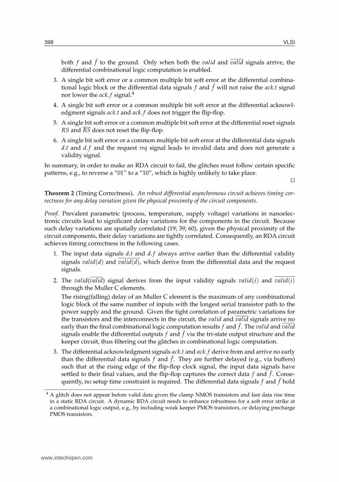
In this section, we first verify the effectiveness of the proposed voltage-controlled nano-addressing circuit (Fig. 8) by running SPICE simulation based on the Stanford CNFET com-pact model (52).In the proposed voltage-controlled nano-addressing circuit, each nanotube is gated by two N-type MOSFET-like CNFETs. These CNFETs are of 6.4nm gate width and 32nm channel length,as are described in the Stanford CNFET compact model. The two CNFETs in each nanotubeare given a voltage drop of Vdd = 1V. The external address voltages are Vdda1 = Vdda2 = 1V,Vssa1 = Vssa2 = 0. As a result, the CNFETs have complementary gate voltages Vg1 +Vg2 = 1V.Fig. 12 gives the nanotube currents in the array with different gate voltage at the first addressline. The nanotubes carry a significant current only with specific gate voltages, e.g., reachingIout = 5.064mA at gate voltage Vg1 = 0.495V.With 0 and 1V external voltages, Fig. 12 gives the currents for all the nanotubes in the array.With larger external voltages, Fig. 12 is extended to give the nanotube currents: any nanotubewith a Vga1 > 1V or Vga2 < 0V gate voltage at the first address line carries zero current.Addressing resolution is given by the difference of addressing voltages between two adjacentnanotubes (since MOSFETs and MOSFET-like CNFETs are limited to a < 60mV/decade in-verse subthreshold slope). Adjusting the external address voltages minimizes any addressinginaccuracy due to manufacturing process and system runtime parametric variations.
6.2 Comparison of CNT Crossbar based and the Existing Nano-Architecture
Let us now compare nano-circuits implemented in the proposed CNT crossbar based nano-architecture and the existing nano-architectures. Considering DNA-guide self-assembly basednanoelectronic architectures such as NANA (42) and SOSA (43) target the far future, and FPNI(50) is very similar to CMOS technology by employing CMOS transistors and nanowires, I willcompare RDG-CNFET based logic implementation with molecular diode and MOS transistorbased logic implementation which is the mainstream nanoelectronic architecture in literature.5
5 Comparing CNFET and CMOS-FET circuits gives approximately 5× performance improvement (16).
www.intechopen.com
����%""
��
��
��
��
��
��
�
�� ��� ��� ��� ��� ��� �� ��� ��� ��
�������
��
�������
������
Fig. 12. Nanotube current Iout in mA for CNFET gate voltage Vg1 in the first address line.
)�� �
� ������
� �
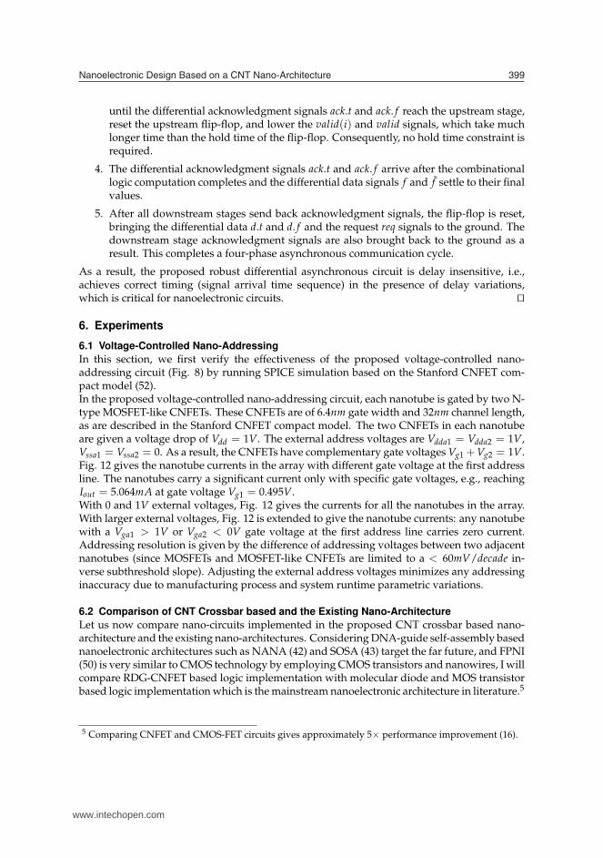
Fig. 13. A molecular diode/MOSFET based Boolean logic a(b + c) implementation.
As an example of a combinational logic block, a Boolean logic function a(b+ c) is implementedbased on RDG-CNFETs (Fig. 6) and by molecular diodes and peripheral CMOS transistors(Fig. 13). In the following experiments, SPICE simulation is conducted based on the latestStanford compact CNFET model (52), a molecular device model from a latest publication (17),and the latest Predictive CMOS Technology Model (45).The RDG-CNFETs are constructed based on an enhancement mode CNFET of 6.4nm gatewidth and 32nm channel length, as is described in the Stanford compact model (52). Thebistable molecules at the front gate provide a resistance difference between GΩ and about80Ω (6).6 The redox active molecules at the back gate are cobalt phthalocyanine (CoPc) (17),which have been the basis of a NW-FET device with 1000× conductance difference (17).The molecular diodes are based on V-shaped amphiphilic [2]rotaxane 54+ molecules (44), withsaturation current Is = 36pA, emission coefficient N = 14.66, and an on/off current ratio of194.9. The CMOS transistors are modeled by 22nm Predictive Technology Models (45). Tobalance the current difference between molecular diodes and PMOS transistors, the PMOStransistors have a channel width/length ratio W/L = 1/10, while each molecular diode con-sists of 10, 000 V-shaped amphiphilic [2]rotaxane 54+ molecules. As a result, the circuit has acurrent on the order of nA.
6 The amorphous silicon based anti-fuse technology works with silicon based nanowires (6). Similartechnologies are expected and assumed here for carbon nanotubes.
www.intechopen.com
������������� ���������������������������������� %"#
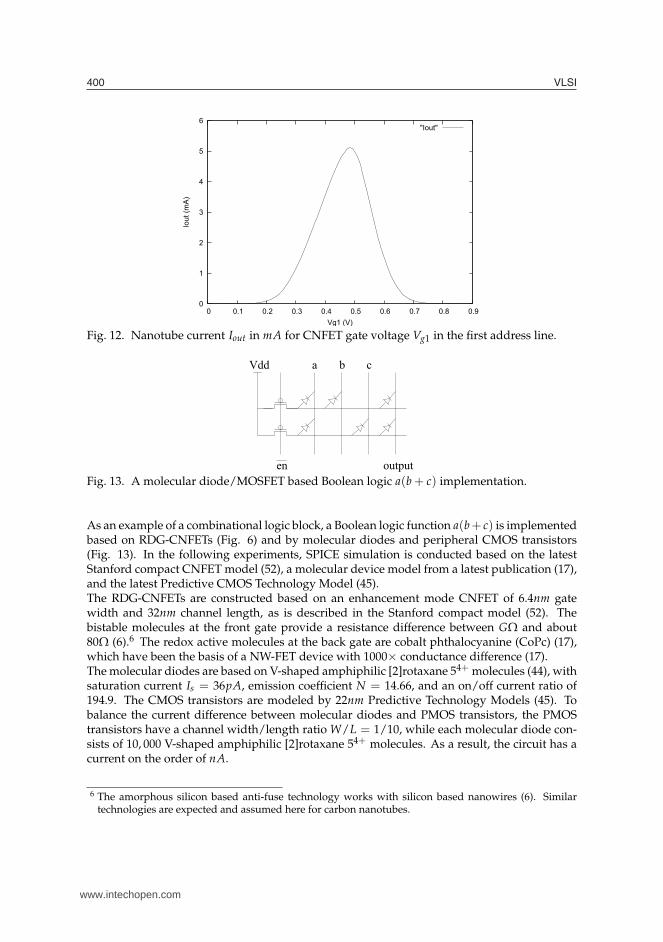
Mo. Diode RDG-CNFETabc Vout Pstatic Vout Pstatic
(V) (W) (V) (W)111 0.999 1.49n 1.000 0.25n110 0.807 0.83µ 1.000 0.33n101 0.807 0.83µ 1.000 0.32n011 0.497 1.45µ 0.000 15.34p000 0.265 1.47µ 0.000 41.32p
Table 1. Output voltage and static power consumption with different inputs of RDG-CNFETand molecular diode based Boolean logic a(b + c) implementations.
Comparing the CNFET based and the molecular diode/CMOS based logic implementations,we have the following observations.
1. Area: The CNFET based logic implementation takes an area of 2 × 6 = 12 CNFETsand 2 × 3 = 6 vias, while molecular diodes and MOSFET based implementation takesan area of 2 × 4 = 8 molecular diodes and 2 MOSFETs (and two more MOSFETs ifan inverter is included at each output to restore signal voltage swing). ConsideringCNFET based implementation is in a complementary logic, and the MOS transistorsdo not scale well, CNFET based implementation is expected to achieve superior logicdensity at a nanometer technology node.
2. Signal reliability: The CNFET based logic implementation achieves full voltage swingat the outputs, while in the diode logic circuit, the output swing depends on the inputs,and varies between 0.503V to 0.735V in the experiment (Table 1). Additional CMOScircuitry (e.g., an inverter) can be included at each output to restore full voltage swing,however, the reduced signal voltage swing in the diode logic circuit still implies com-promised signal reliability.
3. Static power: The CNFET based logic implementation in CMOS logic achieves orders ofmagnitudes of less power consumption compared with molecular diodes and MOSFETbased implementation for most input vectors (Table 1).
4. Performance: The CNFET based logic implementation achieves orders of magnitudeof timing performance improvement compared with molecular diodes and MOSFETbased implementation (Table 2).
In summary, CNFET based logic implementation achieves superior logic density, reliabil-ity, performance, and power consumption compared with molecular diodes and CMOS-FETbased Boolean logic implementation.
6.3 Verification of RDA Circuits
In this section, we verify logic and timing correctness of robust differential asynchronous cir-cuits by running HSPICE simulation based on 22nm Predictive Technology Models (45).Fig. 14 gives signal waveforms for a perfect RDA circuit implementing Boolean function f =ab in CMOS static logic. Input signal a falls from logic 1 at 100ps to logic 0 at 200ps, inputsignal b rises from logic 0 at 0ps to logic 1 at 50ps. The validity signal valid(valid) rises(falls)from logic 0(1) at 100ps to logic 1(0) at 200ps. As a result, we observe that the late arrival ofthe valid(valid) signals enable the combinational logic computation for f and f , and filter out
www.intechopen.com
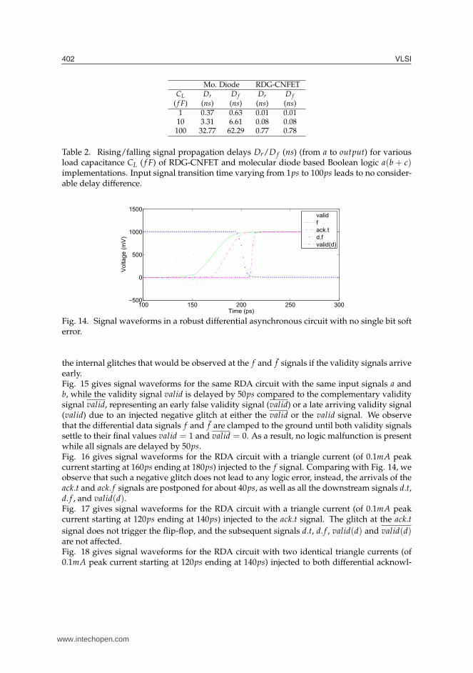
����%"$
Mo. Diode RDG-CNFETCL Dr D f Dr D f
( f F) (ns) (ns) (ns) (ns)1 0.37 0.63 0.01 0.01
10 3.31 6.61 0.08 0.08100 32.77 62.29 0.77 0.78
Table 2. Rising/falling signal propagation delays Dr/D f (ns) (from a to output) for variousload capacitance CL ( f F) of RDG-CNFET and molecular diode based Boolean logic a(b + c)implementations. Input signal transition time varying from 1ps to 100ps leads to no consider-able delay difference.
��� ��� ��� ��� �������
�
���
����
����
���������
���� �������
! ��"
#
$%�
"#
! ��"�"�
Fig. 14. Signal waveforms in a robust differential asynchronous circuit with no single bit softerror.
the internal glitches that would be observed at the f and f signals if the validity signals arriveearly.Fig. 15 gives signal waveforms for the same RDA circuit with the same input signals a andb, while the validity signal valid is delayed by 50ps compared to the complementary validitysignal valid, representing an early false validity signal (valid) or a late arriving validity signal(valid) due to an injected negative glitch at either the valid or the valid signal. We observethat the differential data signals f and f are clamped to the ground until both validity signalssettle to their final values valid = 1 and valid = 0. As a result, no logic malfunction is presentwhile all signals are delayed by 50ps.Fig. 16 gives signal waveforms for the RDA circuit with a triangle current (of 0.1mA peakcurrent starting at 160ps ending at 180ps) injected to the f signal. Comparing with Fig. 14, weobserve that such a negative glitch does not lead to any logic error, instead, the arrivals of theack.t and ack. f signals are postponed for about 40ps, as well as all the downstream signals d.t,d. f , and valid(d).Fig. 17 gives signal waveforms for the RDA circuit with a triangle current (of 0.1mA peakcurrent starting at 120ps ending at 140ps) injected to the ack.t signal. The glitch at the ack.tsignal does not trigger the flip-flop, and the subsequent signals d.t, d. f , valid(d) and valid(d)are not affected.Fig. 18 gives signal waveforms for the RDA circuit with two identical triangle currents (of0.1mA peak current starting at 120ps ending at 140ps) injected to both differential acknowl-
www.intechopen.com
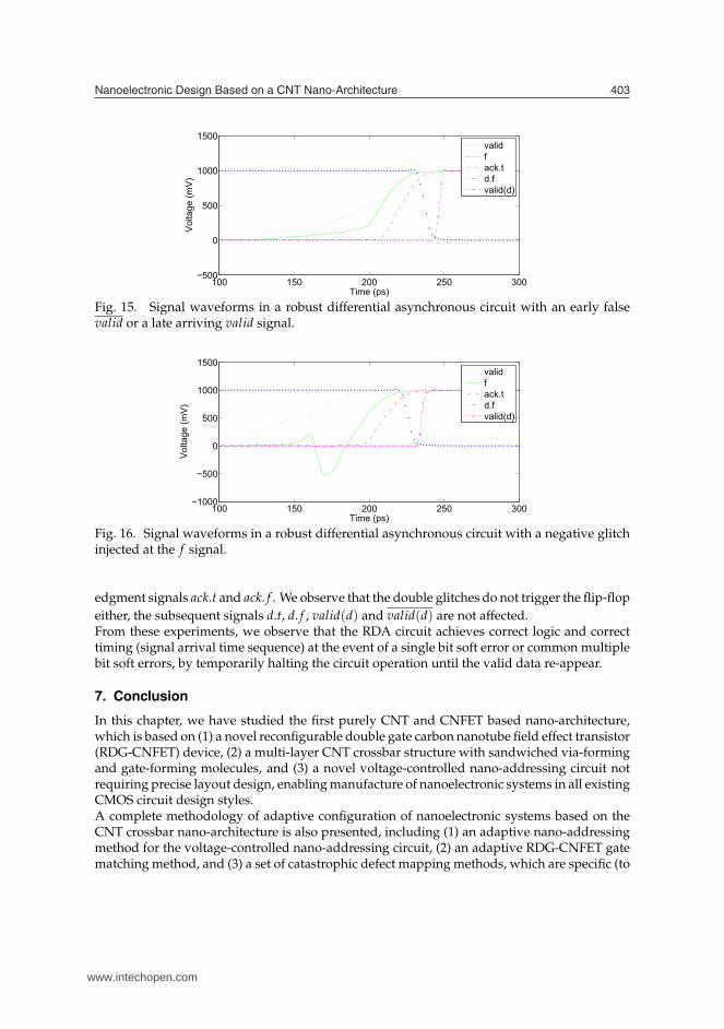
������������� ���������������������������������� %"�
��� ��� ��� ��� �������
�
���
����
����
���������
���� �������
! ��"
#
$%�
"#
! ��"�"�
Fig. 15. Signal waveforms in a robust differential asynchronous circuit with an early falsevalid or a late arriving valid signal.
��� ��� ��� ��� ��������
����
�
���
����
����
���������
���� �������
! ��"
#
$%�
"#
! ��"�"�
Fig. 16. Signal waveforms in a robust differential asynchronous circuit with a negative glitchinjected at the f signal.
edgment signals ack.t and ack. f . We observe that the double glitches do not trigger the flip-flopeither, the subsequent signals d.t, d. f , valid(d) and valid(d) are not affected.From these experiments, we observe that the RDA circuit achieves correct logic and correcttiming (signal arrival time sequence) at the event of a single bit soft error or common multiplebit soft errors, by temporarily halting the circuit operation until the valid data re-appear.
7. Conclusion
In this chapter, we have studied the first purely CNT and CNFET based nano-architecture,which is based on (1) a novel reconfigurable double gate carbon nanotube field effect transistor(RDG-CNFET) device, (2) a multi-layer CNT crossbar structure with sandwiched via-formingand gate-forming molecules, and (3) a novel voltage-controlled nano-addressing circuit notrequiring precise layout design, enabling manufacture of nanoelectronic systems in all existingCMOS circuit design styles.A complete methodology of adaptive configuration of nanoelectronic systems based on theCNT crossbar nano-architecture is also presented, including (1) an adaptive nano-addressingmethod for the voltage-controlled nano-addressing circuit, (2) an adaptive RDG-CNFET gatematching method, and (3) a set of catastrophic defect mapping methods, which are specific (to
www.intechopen.com
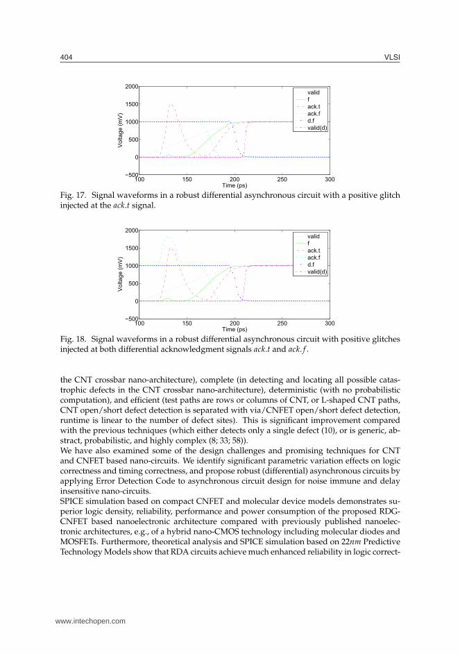
����%"%
��� ��� ��� ��� �������
�
���
����
����
����
���������
���� �������
! ��"
#
$%�
$%#
"#
! ��"�"�
Fig. 17. Signal waveforms in a robust differential asynchronous circuit with a positive glitchinjected at the ack.t signal.
��� ��� ��� ��� �������
�
���
����
����
����
���������
���� �������
! ��"
#
$%�
$%#
"#
! ��"�"�
Fig. 18. Signal waveforms in a robust differential asynchronous circuit with positive glitchesinjected at both differential acknowledgment signals ack.t and ack. f .
the CNT crossbar nano-architecture), complete (in detecting and locating all possible catas-trophic defects in the CNT crossbar nano-architecture), deterministic (with no probabilisticcomputation), and efficient (test paths are rows or columns of CNT, or L-shaped CNT paths,CNT open/short defect detection is separated with via/CNFET open/short defect detection,runtime is linear to the number of defect sites). This is significant improvement comparedwith the previous techniques (which either detects only a single defect (10), or is generic, ab-stract, probabilistic, and highly complex (8; 33; 58)).We have also examined some of the design challenges and promising techniques for CNTand CNFET based nano-circuits. We identify significant parametric variation effects on logiccorrectness and timing correctness, and propose robust (differential) asynchronous circuits byapplying Error Detection Code to asynchronous circuit design for noise immune and delayinsensitive nano-circuits.SPICE simulation based on compact CNFET and molecular device models demonstrates su-perior logic density, reliability, performance and power consumption of the proposed RDG-CNFET based nanoelectronic architecture compared with previously published nanoelec-tronic architectures, e.g., of a hybrid nano-CMOS technology including molecular diodes andMOSFETs. Furthermore, theoretical analysis and SPICE simulation based on 22nm PredictiveTechnology Models show that RDA circuits achieve much enhanced reliability in logic correct-
www.intechopen.com
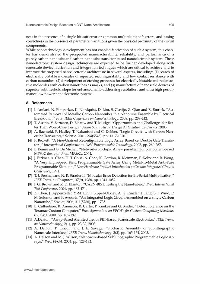
������������� ���������������������������������� %"�
ness in the presence of a single bit soft error or common multiple bit soft errors, and timingcorrectness in the presence of parametric variations given the physical proximity of the circuitcomponents.While nanotechnology development has not enabled fabrication of such a system, this chap-ter has demonstrated the prospected manufacturability, reliability, and performance of apurely carbon nanotube and carbon nanotube transistor based nanoelectronic system. Thesenanoelectronic system design techniques are expected to be further developed along withnanoscale device fabrication and integration techniques which are critical to achieve and toimprove the proposed nanoelectronic architecture in several aspects, including: (1) search ofelectrically bistable molecules of repeated reconfigurability and low contact resistance withcarbon nanotubes, (2) development of etching processes for electrically bistable and redox ac-tive molecules with carbon nanotubes as masks, and (3) manufacture of nanoscale devices ofsuperior subthreshold slope for enhanced nano-addressing resolution, and ultra high perfor-mance low power nanoelectronic systems.
8. References
[1] I. Amlani, N. Pimparkar, K. Nordquist, D. Lim, S. Clavijo, Z. Qian and R. Emrick, “Au-tomated Removal of Metallic Carbon Nanotubes in a Nanotube Ensemble by ElectricalBreakdown,” Proc. IEEE Conference on Nanotechnology, 2008, pp. 239-242.
[2] T. Austin, V. Bertacco, D. Blaauw and T. Mudge, “Opportunities and Challenges for Bet-ter Than Worst-Case Design,” Asian South Pacific Design Automation Conference, 2005.
[3] A. Bachtold, P. Hadley, T. Nakanishi and C. Dekker, “Logic Circuits with Carbon Nan-otube Transistors,” Science, 2001, 294(5545), pp. 1317-1320.
[4] P. Beckett, “A Fine-Grained Reconfigurable Logic Array Based on Double Gate Transis-tors,” International Conference on Field-Programmable Technology, 2002, pp. 260-267.
[5] L. Benini and G. De Micheli, “Networks on chips: A new paradigm for component-basedMPSoC design,” Proc. MPSoC., 2004.
[6] J. Birkner, A. Chan, H. T. Chua, A. Chao, K. Gordon, B. Kleinman, P. Kolze and R. Wong,“A Very High-Speed Field Programmable Gate Array Using Metal-To-Metal Anti-FuseProgrammable Elements,” New Hardware Product Introduction at Custom Integrated CircuitsConference, 1991.
[7] T. J. Brosnan and N. R. Strader II, “Modular Error Detection for Bit-Serial Multiplication,”IEEE Trans. on Computers, 37(9), 1988, pp. 1043-1052.
[8] J. G. Brown and R. D. Blanton, “CAEN-BIST: Testing the NanoFabric,” Proc. InternationalTest Conference, 2004, pp. 462-471.
[9] Z. Chen, J. Appenzeller, Y.-M. Lin, J. Sippel-Oakley, A. G. Rinzler, J. Tang, S. J. Wind, P.M. Solomon and P. Avouris, “An Integrated Logic Circuit Assembled on a Single CarbonNanotube,” Science, 2006, 311(5768), pp. 1735.
[10] B. Culbertson, R. Amerson, R. Carter, P. Kuekes and G. Snider, “Defect Tolerance on theTeramac Custom Computer,” Proc. Symposium on FPGA’s for Custom Computing Machines(FCCM), 2000, pp. 185-192.
[11] A.DeHon, “Array-Based Architecture for FET-Based, Nanoscale Electronics,” IEEE Trans.on Nanotechnology, 2(1), pp. 23-32, 2003.
[12] A. DeHon, P. Lincoln and J. E. Savage, “Stochastic Assembly of SublithographicNanoscale Interface,” IEEE Trans. Nanotechnology, 2(3), pp. 165-174, 2003.
[13] A. DeHon and M. J. Wilson, “Nanowire-Based Sublithographic Programmable Logic Ar-rays,” Proc. FPGA, 2004, pp. 123-132.
www.intechopen.com
����%"�
[14] C. Dwyer, L. Vicci, J. Poulton, D. Erie, R. Superfine, S. Washburn and R. M. Taylor, “Thedesign of DNA self-assembled computing circuitry,” IEEE Trans. on Very Large Scale Inte-gration (VLSI) Systems, 12(11), pp. 1214-1220, Nov. 2004.
[15] D. J. Deleganes, M. Barany, G. Geannopoulos, K. Kreitzer, M. Morrise, D. Milliron, A.P. Singh and S. Wijeratne, “Low-Voltage Swing Logic Circuits for a Pentium 4 ProcessorInteger Core,” IEEE J. of Solid-State Circuits, 40(1), pp. 36-43, 2005.
[16] J. Deng, and H.-S. P. Wong, “A Compact SPICE Model for Carbon Nanotube Field EffectTransistors Including Non-Idealities and Its Application âAT Part II: Full Device Modeland Circuits Performance Benchmarking,” IEEE Trans. Electron Devices, 2007.
[17] X. Duan, Y. Huang and C. M. Lieber, “Nonvolatile Memory and Programmable Logicfrom Molecule-Gated Nanowires,” Nano Letters, 2(5), pp. 487-490, 2002.
[18] D. Ernst, N. S. Kim, S. Das, S. Lee, D. Blaauw, T. Austin, T. Mudge and K. Flautner, “Ra-zor: Circuit-Level Correction of Timing Errors for Low-Power Operation,” IEEE MICROspecial issue on Top Picks From Microarchitecture Conferences of 2004, 2005.
[19] P. Friedberg, Y. Cao, J. Cain, R. Wang, J. Rabaey, and C. Spanos, “Modeling Within-DieSpatial Correlation Effects for Process-Design Co-Optimization,” Proc. International Sym-posium on Quality Electronic Design, pp. 516-521, 2005.
[20] S. C. Goldstein and M. Budiu, “NanoFabrics: Spatial Computing Using Molecular Elec-tronics,” Proc. International Symposium on Computer Architecture, 2001, pp. 178-191.
[21] B. Gojman, E. Rachlin, and J. E. Savage, “Evaluation of Design Strategies for Stochasti-cally Assembled Nanoarray Memories,” Journal of Emerging Technologies, 1(2), 2005, pp.73-108.
[22] J. R. Heath and M. A. Ratner, “Molecular Electronics,” Physics Today, 56(5), pp. 43-49,2003.
[23] S. J. Kang, C. Kocabas, T. Ozel, M. Shim, N. Pimparkar, M. A. Alam, S. V. Rotkin and J. A.Rogers, “High-Performance Electronics Using Dense, Perfectly Aligned Arrays of Single-Walled Carbon Nanotubes,” Nature Nanotechnology, Vol. 2, pp. 230-236, April 2007.
[24] B. S. Landman and R. L. Russo, “On a Pin Versus Block Relationship for Partitions ofLogic Graphs,” IEEE Trans. on Computers, C-20, pp. 1469-1479, 1971.
[25] J. Liu, I. O’Connor, D. Navarro and F. Gaffiot, “Design of a Novel CNTFET-Based Recon-figurable Logic Gate,” Proc. ISVLSI, 2007, pp. 285-290.
[26] B. Liu, “Reconfigurable Double Gate Carbon Nanotube Field Effect Transistor Based Na-noelectronic Architecture,” Proc. Asia and South Pacific Design Automation Conference, 2009.
[27] B. Liu, “Adaptive Voltage Controlled Nanoelectronic Addressing for Yield, Accuracy andResolution,” Proc. International Symposium on Quality Electronic Design, 2009.
[28] B. Liu, “Robust Differential Asynchronous Nanoelectronic Circuits,” Proc. InternationalSymposium on Quality Electronic Design, 2009.
[29] B. Liu, “Defect Mapping and Adaptive Configuration of Nanoelectronic Circuits Basedon a CNT Crossbar Nano-Architecture,” Workshop on Nano, Molecular, and Quantum Com-munications (NanoCom), 2009.
[30] International Technology Roadmap for Semiconductors, http://www.itrs.net/.[31] A. Maheshwari and W. Burleson, “Differential Current-Sensing for On-Chip Intercon-
nects,” IEEE Trans. on VLSI Systems, 12(12), 2004, pp. 1321-1329.[32] P. L. McEuen, M. S. Fuhrer and P. Hongkun, “Single-walled Carbon Nanotube Electron-
ics,” IEEE Trans. Nanotechnology, 1(1), pp. 78-85, 2002.[33] M. Mishra and S. C. Goldstein, “Defect Tolerance at the End of the Roadmap,” Proc.
International Test Conference, 2003, pp. 1201-1211.
www.intechopen.com
������������� ���������������������������������� %"�
[34] S. Mitra, N. Patil and J. Zhang, “Imperfection-Immune Carbon Nanotube VLSI LogicCircuits,” Foundations of NANO, 2008.
[35] T. K. Moon, Error Correction Coding: Mathematical Methods and Algorithms, Wiley-Interscience, 2005.
[36] H. Naeimi and A. DeHon, “A Greedy Algorithm for Tolerating Defective Crosspoints inNanoPLA Design,” Proc. Intl. Conf. on Field-Programmable Technology, 2004, pp. 49-56.
[37] P. Nguyen, H. T. Ng, T. Yamada, M. K. Smith, J. Li, J. Han and M. Meyyappan, “DirectIntegration of Metal Oxide Nanowire in Vertical Field-Effect Transistor,” Nano Letters,2004, 4(4), pp. 651-657.
[38] A. Nieuwoudt and Y. Massoud, “Assessing the Implications of Process Variations on Fu-ture Carbon Nanotube Bundle Interconnect Solutions,” Proc. Intl. Symp. on Quality Elec-tronic Design, 2007, pp. 119-126.
[39] M. Orshansky, L. Milor, P. Chen, K. Keutzer, C. Hu, “Impact of spatial intrachip gatelength variability on the performance of high-speed digital circuits,” IEEE Trans. onComputer-Aided Design of Integrated Circuits and Systems, 2002, pp. 544-553.
[40] S. S. P. Parkin, “Spintronics Materials and Devices: Past, Present and Future,” IEEE Inter-national Electron Devices Meeting (IEDM) Technical Digest, pp. 903-906, 2004.
[41] N. Patil, J. Deng, A. Lin, H.-S. Philip Wong and S. Mitra, “Design Methods for Mis-aligned and Mispositioned Carbon-Nanotube Immune Circuits,” IEEE Tran. on CAD,2008, 27(10), pp. 1725-1736.
[42] J. P. Patwardhan, C. Dwyer, A. R. Lebeck and D. J. Sorin, “NANA: A Nano-Scale ActiveNetwork Architecture,” ACM Journal on Emerging Technologies in Computing Systems, 2(1),pp. 1-30, 2006.
[43] J. P. Patwardhan, V. Johri, C. Dwyer and A. R. Lebeck, “A Defect Tolerant Self-OrganizingNanoscale SIMD Architecture,” International Conference on Architecture Support for Pro-gramming Languages and Operating Systems, 2006, pp. 241-251.
[44] A. R. Pease, J. O. Jeppesen, J. F. Stoddart, Y. Luo, C. P. Collier and J. R. Heath, “SwitchingDevices Based on Interlocked Molecules,” Acc. Chem. Res., 34, pp. 433-444, 2001.
[45] Predictive Technology Model, http://www.eas.asu.edu/∼ptm/.[46] A. Raychowdhury and K. Roy, “Carbon Nanotube Electronics: Design of High Perfor-
mance and Low Power Digital Circuits,” IEEE Trans. on Circuits and Systems - I: Funda-mental Theory and Applications, 54(11), pp. 2391-1401, 2007.
[47] G. S. Rose, A. C. Cabe, N. Gergel-Hackett, N. Majumdar, M. R. Stan, J. C. Bean, L. R. Har-riott, Y. Yao and J. M. Tour, “Design Approaches for Hybrid CMOS/Molecular MemoryBased on Experimental Device Data,” Proc. Great Lakes Symposium on VLSI, 2006, pp. 2-7.
[48] J. E. Savage, E. Rachlin, A. DeHon, C. M. Lieber and Y. Wu, “Radial Addressing ofNanowires,” ACM Journal of Emerging Technologies in Computing Systems, 2(2), pp. 129-154. 2006.
[49] M. S. Schmidt, T. Nielsen, D. N. Madsen, A. Kristensen and P. BÃÿggild, “Nano-ScaleSilicon structures by Using Carbon Nanotubes as Reactive Ion Masks,” Nanotechnology,16, pp. 750-753, 2005.
[50] G. S. Snider and R. S. Williams, “Nano/CMOS Architectures Using a Field-Programmable Nanowire Interconnect,” Nanotechnology, 18(3), 2007.
[51] M. R. Stan, P. D. Franzon, S. C. Goldstein, J. C. Lach and M. M. Ziegler, “MolecularElectronics: From Devices and Interconnect to Circuits and Architecture,” Proc. of theIEEE, 91(11), pp. 1940-1957, 2003.
[52] Stanford CNFET Model, http://nano.stanford.edu/models.php.
www.intechopen.com

����%"
[53] R. Sordan, K. Balasubramanian, M. Burghard and K. Kern, “Exclusive-OR Gate with aSingle Carbon Nanotube,” Appl. Phys. Lett., 2006, 88.
[54] D. B. Strukov and K. K. Likharev, “CMOL FPGA: A Reconfigurable Architecture for Hy-brid Digital Circuits with Two-Terminal Nanodevices,” Nanotechnology, 16(6), pp. 888-900, 2005.
[55] J. P. Sun, G. I. Haddad, P. Mazumder and J. N. Schulman, “Resonant Tunneling Diodes:Models and Properties,” Proc. of the IEEE, 86(4), 1998, pp. 641-660.
[56] Y.-C. Tseng, P. Xuan, A. Javey, R. Malloy, Q. Wang, J. Bokor and H. Dai, “MonolithicIntegration of Carbon Nanotube Devices with Silicon MOS Technology,” Nano Letters,4(1), pp. 123-127, 2004.
[57] N. Tzartzanis and W. W. Walker, “Differential Current-Mode Sensing for Efficient On-Chip Global Signaling,” IEEE J. of Solid-State Circuits, 40(11), 2005, pp. 2141-2147.
[58] Z. Wang and K. Chakrabarty, “Using Built-In Self-Test and Adaptive Recovery for DefectTolerance in Molecular Electronics-Based NanoFabrics,” Proc. International Test Confer-ence, 2005.
[59] R. S. Williams and P. J. Kuekes, “Demultiplexer for a Molecular Wire Crossbar Network,”US Patent Number 6,256,767, 2001.
[60] J. Xiong, V. Zolotov, and L. He, “Robust Extraction of Spatial Correlation,” Proc. Interna-tional Symposium on Physical Design, 2006, pp. 2-9.
[61] J. Zhang, N. P. Patil, A. Hazeghi and S. Mitra, “Carbon Nanotube Circuits in the Presenceof Carbon Nanotube Density Variations,” Proc. Design Automation Conference, 2009.
[62] J. Zhang, N. P. Patil and S. Mitra, “Design Guidelines for Metallic-Carbon-Nanotube-Tolerant Digital Logic Circuits, Proc. Design Automation and Test in Europe, 2008, pp. 1009-1014.
[63] W. Zhang, N. K. Jha and L. Shang, “NATURE: A Hybrid Nanotube/CMOS DynamicallyReconfigurable Architecture,” Proc. Design Automation Conference, 2006, pp. 711-716.
[64] G. Zhang, P. Qi, X. Wang, Y. Lu, X. Li, R. Tu, S. Bangsaruntip, D. Mann, L. Zhang and H.Dai, “Selective Etching of Metallic Carbon Nanotubes by Gas-Phase Reaction,” Science,314, 2006, pp. 974-977.
www.intechopen.com
VLSIEdited by Zhongfeng Wang
ISBN 978-953-307-049-0Hard cover, 456 pagesPublisher InTechPublished online 01, February, 2010Published in print edition February, 2010
The process of Integrated Circuits (IC) started its era of VLSI (Very Large Scale Integration) in 1970’s whenthousands of transistors were integrated into one single chip. Nowadays we are able to integrate more than abillion transistors on a single chip. However, the term “VLSI” is still being used, though there was some effort tocoin a new term ULSI (Ultra-Large Scale Integration) for fine distinctions many years ago. VLSI technology hasbrought tremendous benefits to our everyday life since its occurrence. VLSI circuits are used everywhere, realapplications include microprocessors in a personal computer or workstation, chips in a graphic card, digitalcamera or camcorder, chips in a cell phone or a portable computing device, and embedded processors in anautomobile, et al. VLSI covers many phases of design and fabrication of integrated circuits. For a commercialchip design, it involves system definition, VLSI architecture design and optimization, RTL (register transferlanguage) coding, (pre- and post-synthesis) simulation and verification, synthesis, place and route, timinganalyses and timing closure, and multi-step semiconductor device fabrication including wafer processing, diepreparation, IC packaging and testing, et al. As the process technology scales down, hundreds or eventhousands of millions of transistors are integrated into one single chip. Hence, more and more complicatedsystems can be integrated into a single chip, the so-called System-on-chip (SoC), which brings to VLSIengineers ever increasingly challenges to master techniques in various phases of VLSI design. For modernSoC design, practical applications are usually speed hungry. For instance, Ethernet standard has evolved from10Mbps to 10Gbps. Now the specification for 100Mbps Ethernet is on the way. On the other hand, with thepopularity of wireless and portable computing devices, low power consumption has become extremely critical.To meet these contradicting requirements, VLSI designers have to perform optimizations at all levels ofdesign. This book is intended to cover a wide range of VLSI design topics. The book can be roughly partitionedinto four parts. Part I is mainly focused on algorithmic level and architectural level VLSI design and optimizationfor image and video signal processing systems. Part II addresses VLSI design optimizations for cryptographyand error correction coding. Part III discusses general SoC design techniques as well as other application-specific VLSI design optimizations. The last part will cover generic nano-scale circuit-level design techniques.
How to referenceIn order to correctly reference this scholarly work, feel free to copy and paste the following:
Bao Liu (2010). Nanoelectronic Design Based on a CNT Nano-Architecture, VLSI, Zhongfeng Wang (Ed.),ISBN: 978-953-307-049-0, InTech, Available from: http://www.intechopen.com/books/vlsi/nanoelectronic-design-based-on-a-cnt-nano-architecture
www.intechopen.com

InTech EuropeUniversity Campus STeP Ri Slavka Krautzeka 83/A 51000 Rijeka, Croatia Phone: +385 (51) 770 447 Fax: +385 (51) 686 166www.intechopen.com
InTech ChinaUnit 405, Office Block, Hotel Equatorial Shanghai No.65, Yan An Road (West), Shanghai, 200040, China
Phone: +86-21-62489820 Fax: +86-21-62489821