Nano
44
DESIGN A ND SIMULATION OF NANO SCAL E N M OS DEVICE A PROJECT REPORT Submitted by Bhargab Kashyap Manish jha Suvanjan Nandy Ranvijay Kumar Singh Mousumi Biswas Himadri Prasad Das Jiaul Hoque in partial fulfillment for the award of the degree of B.TECH IN Electronics & Communication Engineering INSTITUTE OF SCIENCE & TECHNOLOGY May, 2011 UNDER THE GUIDANCE OF Himadri Sekhar Das ASST. PROFESSOR Department of Electronics & Communication Engineering INSTITUTE OF SCIENCE & TECHNOLOGY
-
Upload
subir-maity -
Category
Documents
-
view
22 -
download
1
description
Nano scale mos
Transcript of Nano

7/14/2019 Nano
http://slidepdf.com/reader/full/nano55cf9d2d550346d033ac8bf6 1/44
D E SI G N AN D SI M U L AT I O N OF N AN O
SCAL E N-M OS D E VI CE
A PROJECT REPORT
Submitted by
Bhargab Kashyap
Manish jha
Suvanjan Nandy
Ranvijay Kumar Singh
Mousumi Biswas
Himadri Prasad Das
Jiaul Hoque
in partial fulfillment for the award of the degree
of
B.TECH
IN
Electronics & Communication Engineering
INSTITUTE OF SCIENCE & TECHNOLOGY
May, 2011
UNDER THE GUIDANCE OF
Himadri Sekhar DasASST. PROFESSOR
Department of Electronics & Communication Engineering
INSTITUTE OF SCIENCE & TECHNOLOGY

7/14/2019 Nano
http://slidepdf.com/reader/full/nano55cf9d2d550346d033ac8bf6 2/44
ABSTRACT
Increased demand for high performance, low power and higher density is
continuously passing the fabrication process to go beyond ultra deep (UDSM)
technologies. As the downscaling continuous it becomes harder to fabricate
devices without compromising performance due to undesirable short channel
effect (SCEs), which restrict further downscaling of the device. The
predominant SCEs are drain induced barrier lowering (DIBL), two dimensional
charge sharing(CS) channel modulation, carrier velocity saturation, impact
ionization, hot carrier effects etc.
In our project work we are wiling to make a n-mos device of 0.18um gate
length and compare the performance with that of convention mosfet.
Computer simulations have emerged as a very elegant way to aid process
and device engineer in their task of finding an optimum process. Process and
device simulation is commonly used for the design of new very large scale
integration (VLSI) devices and processes. Simulation programs serves as
exploratory tools in order to gain better understanding of process and device
physics. We are using for process and device simulation using Technology
Computer Aided Design(TCAD).

7/14/2019 Nano
http://slidepdf.com/reader/full/nano55cf9d2d550346d033ac8bf6 3/44
ACKNOWLEDGEMENT
With great pleasure I would like to express deep gratitude to Mr.Himadri Sekhar Das, Lecturer, Department of Electronics & Communication, Institute of Science & Technology, for the help, cooperation and guidance received from him throughout
the tenure of this seminar. His valuable and constructive suggestions at many difficultsituations are immensely acknowledged.
I am deeply indebted to Mr. Himadri Sekhar Das, Lecturer,
Department of Electronics & Communication for providing a mentally simulating environment
and for many hours of enjoyable discussion. In spite of his busy schedules, his frequent
valuable advice and master suggestions at every stage lead to a systematic approach in
completing this seminar.
My sincere obligation goes to Mr. Subir Kumar Maity, H.O.D.,
Department of Electronics & communication, Institute Of Science & Technology for his
constant support.
Regards…………………………………..Manish Kumar JhaBhargab KashyapSuvanjan NandyRanvijay Kumar SinghMousumi BiswasJiaul HoqueHimadri Prasad Das
C O N T E N T S1. Metal Oxide Semiconductor Technology Page- 4-14
1.1 Introduction Page- 41.2 MOSFET: Circuits Symbols & MOS structure Page- 4
1.2.1 MOSFET operation Page- 61.2.2 Metal-Oxide-Semiconductor structure Page- 6
1.3 Modes of operation Page- 91.4 Threshold Voltage Page- 13
2. MOSFET: Scaling Page- 15-26
2.1 Introduction Page- 152.2 Reasons for MOSFET scaling Page- 15
2.2.1 Moore’s Law Page- 16
2.3 Difficulties arising due to MOSFET size reduction Page- 18
2.3.1 Higher subthreshold conduction Page- 18
2.3.2 Increased gate-oxide leakage Page- 18
2.3.3 Increased junction leakage Page- 19
2.3.4 Lower output resistance Page- 19

7/14/2019 Nano
http://slidepdf.com/reader/full/nano55cf9d2d550346d033ac8bf6 4/44
2.3.5 Lower transconductance Page- 20
2.3.6 Interconnect capacitance Page- 202.3.7 Heat production Page- 202.3.8 Process variations Page- 212.3.9 Modeling challenges Page- 21
2.4 Scaling Page- 222.5 Scaling Factors Page- 22
2.6 Scaling Factors for Device Parameters Page- 222.7 Scaling of Interconnects Page- 23
2.8 MOSFET Scaling Laws Page- 23 2.8.1 Constant voltage scaling Page- 24 2.8.2 Constant field scaling Page- 25
2.9 Problems Of Scaling Page- 26
3. Short Channel Effect Page- 27-33
3.1 Introduction Page- 273.2 Types Of Short Channel Effects Page- 27
3.2.1 Drain-induced barrier lowering and
punch through Page- 283.2.2 Surface scattering Page- 283.2.3 Velocity saturation Page- 293.2.4 Impact ionization Page- 303.2.5 Hot electrons Page- 30
4. Simulation of nano scaled n-mos device Page- 34-544.1 Process Simulation Page- 354.2 Fabrication Process in ATHENA Page- 35
4.2.1 Defining initial grid Page- 364.2.2 ATHENA Deposit Code Page- 384.2.3Vt Adjust Implant Code Page- 384.2.4 Heavy Drain/Source Doping Code Page- 39
4.2.5 Specification of Electrodes in ATHENA Page- 414.3 ATLAS Page- 434.3.1 Elements of ATLAS Input Deck Page- 444.3.2 ATLAS input and output Page- 45
4.4 Project Programming Page- 464.5 Improvement and results after simulation of NMOS Page- 52
REFERENCES Page- 55APPENDICES Page- 56REFERENCES Page- 57
List of TablesTable 1: Year Linewidth Clockspeed Page- 25
List of Figures
Chapter 1Chapter 2 Chapter 3 Chapter 4
Figure 1:Mos Signs
Figure 2:Application& mos structure
Figure 3:MOS in on & off state
Figure 4:I-V curve of MOS
Figure 5:MOSstructure
Figure 8:Technologymovement
Figure 9:Moore’s Law
Figure 10:CurrentMirror
Figure 11:Heat Sinks
Figure 12:channelaccess for constantvoltage scaling
Figure 13:Inversion & depleyion region
Figure 14:MOSInternal Structure
Figure 15:Disectionof MOS
Figure 16: flow chart
Figure 17:Meshstructure
Figure 18:Dopingconcentration of MOS
Figure 19:Athenamirror
Figure 20 & 21:Electrode Define

7/14/2019 Nano
http://slidepdf.com/reader/full/nano55cf9d2d550346d033ac8bf6 5/44
Figure 6:Ohmicrehion
Figure 7:Thresoldvoltage
Figure 22:ATLAS I/O
Figure 23,24,25:I-Vcurves
Figure 26:DIBL curve
Chapter
1
Metal Oxide S emconductor T echnology
M OSFET the word consist of ‘MOS’ & ‘FET’. ‘FET’ is Field Effect Transistor. And ‘MOS’
implies Metal Oxide Semiconductor. Metal–oxide–semiconductor field-effect
transistor (MOSFET, MOS-FET, or MOS FET) is a device used to amplify or switch electronic signals. The
basic principle of the device was first proposed by Julius Edgar Lilienfeld in 1925. In MOSFETs, a voltage
on the oxide-insulated gate electrode can induce a conducting channel between the two other contacts
called source and drain. The channel can be of n-type or p-type (see article on semiconductor devices),
and is accordingly called an nMOSFET or a pMOSFET (also commonly nMOS, pMOS). It is by far the most
common transistor in both digital and analog circuits, though the bipolar junction transistor was at one
time much more common.
The 'metal' in the name is now often a misnomer because the previously metal gate material is now often
a layer of polysilicon (polycrystalline silicon). Aluminium had been the gate material until the mid1970s,
when polysilicon became dominant, due to its capability to form self-aligned gates. Metallic gates are
regaining popularity, since it is difficult to increase the speed of operation of transistors without metal
gates.
IGFET is a related term meaning insulated-gate field-effect transistor, and is almost synonymous with
MOSFET, though it can refer to FETs with a gate insulator that is not oxide. Another synonym
is MISFET for metal–insulator–semiconductor FET.

7/14/2019 Nano
http://slidepdf.com/reader/full/nano55cf9d2d550346d033ac8bf6 6/44
1.2 MOSFET: Circuits Symbols & MOS structure
A variety of symbols are used for the MOSFET. The basic design is generally a line for the
channel with the source and drain leaving it at right angles and then bending back at right
angles into the same direction as the channel. Sometimes three line segments are used for
enhancement mode and a solid line for depletion mode. Another line is drawn parallel to the
channel for the gate.
The bulk connection, if shown, is shown connected to the back of the channel with an arrow
indicating PMOS or NMOS. Arrows always point from P to N, so an NMOS (N-channel in P-
well or P-substrate) has the arrow pointing in (from the bulk to the channel). If the bulk is
connected to the source (as is generally the case with discrete devices) it is sometimes angled
to meet up with the source leaving the transistor. If the bulk is not shown (as is often the case
in IC design as they are generally common bulk) an inversion symbol is sometimes used toindicate PMOS, alternatively an arrow on the source may be used in the same way as for
bipolar transistors (out for nMOS, in for pMOS).
Comparison of enhancement-mode and depletion-mode MOSFET symbols, along
with JFET symbols (drawn with source and drain ordered such that higher voltages appear
higher on the page than lower voltages):
Figure 1:
P-channel
N-channel
JFET MOSFET enh MOSFET enh (no bulk) MOSFET dep
For the symbols in which the bulk, or body, terminal is shown, it is here shown internally
connected to the source. This is a typical configuration, but by no means the only important
configuration. In general, the MOSFET is a four-terminal device, and in integrated circuits
many of the MOSFETs share a body connection, not necessarily connected to the source
terminals of all the transistors.

7/14/2019 Nano
http://slidepdf.com/reader/full/nano55cf9d2d550346d033ac8bf6 7/44
1.2.1 MOSFET operation
Example application of an N-Channel MOSFET. When the switch is pushed the LED lights
up.[2]
Metal–oxide–semiconductor structure on P-type silicon
Figure 2
1.2.2 Metal–oxide–semiconductor structure
A traditional metal–oxide–semiconductor (MOS) structure is obtained by growing a layer of silicon dioxide
(SiO2) on top of a silicon substrate and depositing a layer of metal or polycrystalline silicon (the latter is
commonly used). As the silicon dioxide is a dielectric material, its structure is equivalent to a
planar capacitor, with one of the electrodes replaced by a semiconductor.
When a voltage is applied across a MOS structure, it modifies the distribution of charges in the
semiconductor. If we consider a P-type semiconductor (with N A the density of acceptors, p the density of
holes; p = N A in neutral bulk), a positive voltage, V GB, from gate to body (see figure) creates a depletion
layer by forcing the positively charged holes away from the gate-insulator/semiconductor interface,
leaving exposed a carrier-free region of immobile, negatively charged acceptor ions (see doping
(semiconductor)). If V GB is high enough, a high concentration of negative charge carriers forms in
an inversion layer located in a thin layer next to the interface between the semiconductor and the
insulator. Unlike the MOSFET, where the inversion layer electrons are supplied rapidly from the
source/drain electrodes, in the MOS capacitor they are produced much more slowly by thermal generation
through carrier generation and recombination centers in the depletion region. Conventionally, the gate
voltage at which the volume density of electrons in the inversion layer is the same as the volume density
of holes in the body is called the threshold voltage.
This structure with P-type body is the basis of the N-type MOSFET, which requires the addition of an N-
type source and drain regions.

7/14/2019 Nano
http://slidepdf.com/reader/full/nano55cf9d2d550346d033ac8bf6 8/44
MOSFET structure and channel formation
Cross section of an NMOS without channel formed: OFF state
Cross section of an NMOS with channel formed: ON state Figure 3
A metal–oxide–semiconductor field-effect transistor (MOSFET) is based on the modulation of charge
concentration by a MOS capacitance between a body electrode and a gate electrode located above the
body and insulated from all other device regions by a gate dielectric layer which in the case of a MOSFET
is an oxide, such as silicon dioxide. If dielectrics other than an oxide such as silicon dioxide (often referred
to as oxide) are employed the device may be referred to as a metal–insulator–semiconductor FET
(MISFET). Compared to the MOS capacitor, the MOSFET includes two additional terminals
(source and drain), each connected to individual highly doped regions that are separated by the body
region. These regions can be either p or n type, but they must both be of the same type, and of opposite
type to the body region. The source and drain (unlike the body) are highly doped as signified by a '+' sign
after the type of doping.
If the MOSFET is an n-channel or nMOS FET, then the source and drain are 'n+' regions and the body is a
'p' region. As described above, with sufficient gate voltage, holes from the body are driven away from the
gate, forming an inversion layer or n-channel at the interface between the p region and the oxide. This
conducting channel extends between the source and the drain, and current is conducted through it when a
voltage is applied between source and drain.
For gate voltages below the threshold value, the channel is lightly populated, and only a very small sub
threshold leakage current can flow between the source and the drain.
If the MOSFET is a p-channel or pMOS FET, then the source and drain are 'p+' regions and the body is a
'n' region. When a negative gate-source voltage (positive source-gate) is applied, it creates a p-channel at
the surface of the n region, analogous to the n-channel case, but with opposite polarities of charges and
voltages. When a voltage less negative than the threshold value (a negative voltage for p-channel) is

7/14/2019 Nano
http://slidepdf.com/reader/full/nano55cf9d2d550346d033ac8bf6 9/44
applied between gate and source, the channel disappears and only a very small sub threshold current can
flow between the source and the drain.
The source is so named because it is the source of the charge carriers (electrons for n-channel, holes for
p-channel) that flow through the channel; similarly, the drain is where the charge carriers leave the
channel.
The device may comprise a Silicon On Insulator (SOI) device in which a Buried OXide (BOX) is formed
below a thin semiconductor layer. If the channel region between the gate dielectric and a Buried Oxide
(BOX) region is very thin, the very thin channel region is referred to as an Ultra Thin Channel (UTC)
region with the source and drain regions formed on either side thereof in and/or above the thin
semiconductor layer. Alternatively, the device may comprise a SEMiconductor. On Insulator (SEMOI)
device in which semiconductors other than silicon are employed. Many alternative semiconductor
materials may be employed.
When the source and drain regions are formed above the channel in whole or in part, they are referred to
as Raised Source/ Drain (RSD) regions.
1.3 Modes of operation
The operation of a MOSFET can be separated into three different modes, depending on the voltages at the
terminals. In the following discussion, a simplified algebraic model is used that is accurate only for old
technology. Modern MOSFET characteristics require computer models that have rather more complex
behavior.
For an enhancement-mode, n-channel MOSFET, the three operational modes are:
Cutoff, sub threshold, or weak-inversion mode
When V GS < V th:
Where V th is the threshold voltage of the device.
According to the basic threshold model, the transistor is turned off, and there is no
conduction between drain and source. In reality, the Boltzmann distribution of electron
energies allows some of the more energetic electrons at the source to enter the channel
and flow to the drain, resulting in a sub threshold current that is an exponential function
of gate–source voltage. While the current between drain and source should ideally be
zero when the transistor is being used as a turned-off switch, there is a weak-inversion
current, sometimes called sub threshold leakage.
In weak inversion the current varies exponentially with gate-to-source bias V GS as given
approximately by:
,
where I D0 = current at V GS = V th and the slope factor n is given by
n = 1 + C D / C OX ,
with C D = capacitance of the depletion layer and C OX = capacitance of the oxide layer.
In a long-channel device, there is no drain voltage dependence of the current

7/14/2019 Nano
http://slidepdf.com/reader/full/nano55cf9d2d550346d033ac8bf6 10/44
once V DS > > V T , but as channel length is reduced drain-induced barrier
lowering introduces drain voltage dependence that depends in a complex way upon the
device geometry (for example, the channel doping, the junction doping and so on).
Frequently, threshold voltage Vth for this mode is defined as the gate voltage at which a
selected value of current ID0 occurs, for example, ID0 = 1 µA, which may not be the
same Vth-value used in the equations for the following modes.
Some micropower analog circuits are designed to take advantage of sub threshold
conduction. By working in the weak-inversion region, the MOSFETs in these circuits
deliver the highest possible transconductance-to-current ratio, namely: gm / I D = 1 /
(nV T ), almost that of a bipolar transistor.
The sub threshold I–V curve depends exponentially upon threshold voltage, introducing
a strong dependence on any manufacturing variation that affects threshold voltage; for
example: variations in oxide thickness, junction depth, or body doping that change the
degree of drain-induced barrier lowering. The resulting sensitivity to fabricational
variations complicates optimization for leakage and performance.
Figure 4
MOSFET drain current vs. drain-to-source voltage for several values of V GS − V th; the
boundary between linear (Ohmic) and saturation (active) modes is indicated by the upward
curving parabola.
Figure 5
Cross section of a MOSFET operating in the linear (Ohmic) region; strong inversion region
present even near drain

7/14/2019 Nano
http://slidepdf.com/reader/full/nano55cf9d2d550346d033ac8bf6 11/44
Cross section of a MOSFET operating in the saturation (active) region; channel exhibits pinch-
off near drain Figure 6
Triode mode or linear region (also known as the ohmic mode)
When V GS > V th and V DS < ( V GS - V th )
The transistor is turned on, and a channel has been created which allows current to flow
between the drain and the source. The MOSFET operates like a resistor, controlled by
the gate voltage relative to both the source and drain voltages. The current from drain to
source is modeled as:
where µn is the charge-carrier effective mobility, W is the gate width, L is the gate
length and C ox is the gate oxide capacitance per unit area. The transition from the
exponential sub threshold region to the triode region is not as sharp as the equations
suggest.
Saturation or active mode:
When V GS > V th and V DS > ( V GS - V th )
The switch is turned on, and a channel has been created, which allows current to flow
between the drain and source. Since the drain voltage is higher than the gate voltage,
the electrons spread out, and conduction is not through a narrow channel but through a
broader, two- or three-dimensional current distribution extending away from the
interface and deeper in the substrate. The onset of this region is also known as pinch-
off to indicate the lack of channel region near the drain. The drain current is now
weakly dependent upon drain voltage and controlled primarily by the gate–source
voltage, and modeled very approximately as:
The additional factor involving λ, the channel-length modulation parameter, models
current dependence on drain voltage due to the Early effect, or channel length

7/14/2019 Nano
http://slidepdf.com/reader/full/nano55cf9d2d550346d033ac8bf6 12/44
modulation. According to this equation, a key design parameter, the MOSFET
transconductance is:
,
Where the combination V ov = V GS - V th is called the overdrive voltage. Another keydesign parameter is the MOSFET output resistance r O given by:
.
r out is the inverse of gds where . VDS is the expression in saturation
region.
If λ is taken as zero, an infinite output resistance of the device results that leads to
unrealistic circuit predictions, particularly in analog circuits.
As the channel length becomes very short, these equations become quite inaccurate.
New physical effects arise. For example, carrier transport in the active mode may
become limited by velocity saturation. When velocity saturation dominates, the
saturation drain current is more nearly linear than quadratic in VGS. At even shorter
lengths, carriers transport with near zero scattering, known as quasi-ballistic transport.
In addition, the output current is affected by drain-induced barrier lowering of the
threshold voltage.
1.4 Threshold Voltage
Depletion region of an nMOSFET biased below threshold

7/14/2019 Nano
http://slidepdf.com/reader/full/nano55cf9d2d550346d033ac8bf6 13/44
Depletion region of an nMOSFET biased above threshold with channel formed
Simulation result for formation of inversion channel (electron density) and attainment of
threshold voltage (IV) in a nanowire MOSFET. Note that the threshold voltage for this device
lies around 0.45V. Figure 7
The threshold voltage of a MOSFET is usually defined as the gate voltage where an inversion layer forms
at the interface between the insulating layer (oxide) and the substrate (body) of the transistor. The
creation of this layer is described next.
In an n-MOSFET the substrate of the transistor is composed of p-type silicon (see doping
(semiconductor)), which has positively charged mobile holes as carriers. When a positive voltage is
applied on the gate, an electric field causes the holes to be repelled from the interface, creating a
depletion region containing immobile negatively charged acceptor ions. A further increase in the gate
voltage eventually causes electrons to appear at the interface, in what is called an inversion layer, or
channel. Historically the gate voltage at which the electron density at the interface is the same as the hole
density in the neutral bulk material is called the threshold voltage. Practically speaking the threshold
voltage is the voltage at which there are sufficient electrons in the inversion layer to make a low
resistance conducting path between the MOSFET source and drain.
In the figures, the source (left side) and drain (right side) are labeled n+ to indicate heavily doped (blue)
n-regions. The depletion layer dopant is labeled N A− to indicate that the ions in the (pink) depletion layer
are negatively charged and there are very few holes. In the (red) bulk the number of holes p = N A making
the bulk charge neutral.
If the gate voltage is below the threshold voltage (top figure), the transistor is turned off and ideally there
is no current from the drain to the source of the transistor. In fact, there is a current even for gate biases
below threshold (sub threshold leakage) current, although it is small and varies exponentially with gate
bias. If the gate voltage is above the threshold voltage (lower figure), the transistor is turned on, due to
there being many electrons in the channel at the oxide-silicon interface, creating a low-resistance channel

7/14/2019 Nano
http://slidepdf.com/reader/full/nano55cf9d2d550346d033ac8bf6 14/44
where charge can flow from drain to source. For voltages significantly above threshold, this situation is
called strong inversion. The channel is tapered when V D > 0 because the voltage drop due to the current
in the resistive channel reduces the oxide field supporting the channel as the drain is approached.
In modern devices the threshold voltage is a much less clear-cut parameter subject to variation with the
biases applied to the device; see drain induced barrier lowering.
Chapter
2
S caling & T heir P roblems
O ver the past decades, the MOSFET has continually been scaled down in size;
typical MOSFET channel lengths were once several micrometers, but modern integrated
circuits are incorporating MOSFETs with channel lengths of tens of nanometers. Intel began
production of a process featuring a 32 nm feature size (with the channel being even shorter) in
late 2009. The semiconductor industry maintains a "roadmap", the ITRS, which sets the pace
for MOSFET development. Historically, the difficulties with decreasing the size of the
MOSFET have been associated with the semiconductor device fabrication process, the need to
use very low voltages, and with poorer electrical performance necessitating circuit redesign
and innovation (small MOSFETs exhibit higher leakage currents, and lower output resistance,
discussed below).
2.2 Reasons for MOSFET scaling
Smaller MOSFETs are desirable for several reasons. The main reason to make transistors smaller is to
pack more and more devices in a given chip area. This results in a chip with the same functionality in a
smaller area, or chips with more functionality in the same area. Since fabrication costs for
a semiconductor wafer are relatively fixed, the cost per integrated circuits is mainly related to the number
of chips that can be produced per wafer. Hence, smaller ICs allow more chips per wafer, reducing the
price per chip. In fact, over the past 30 years the number of transistors per chip has been doubled every
2–3 years once a new technology node is introduced. For example the number of MOSFETs in a
microprocessor fabricated in a 45 nm technology is twice as many as in a 65 nm chip. This doubling of the
transistor count was first observed by Gordon Moore in 1965 and is commonly referred to as Moore's law.

7/14/2019 Nano
http://slidepdf.com/reader/full/nano55cf9d2d550346d033ac8bf6 15/44
Figure 8: Trend of Intel CPU transistor gate length
It is also expected that smaller transistors switch faster. For example, one approach to size reduction is a
scaling of the MOSFET that requires all device dimensions to reduce proportionally. The main device
dimensions are the transistor length, width, and the oxide thickness, each (used to) scale with a factor of
0.7 per node. This way, the transistor channel resistance does not change with scaling, while gate
capacitance is cut by a factor of 0.7. Hence, the RC delay of the transistor scales with a factor of 0.7.
While this has been traditionally the case for the older technologies, for the state-of-the-art MOSFETs
reduction of the transistor dimensions does not necessarily translate to higher chip speed because the
delay due to interconnections is more significant.
2.2.1 Moore’s Law
According to Moore’s Law, the number of transistors on a chip roughly doubles every
two years. As a result the scale gets smaller and smaller. For decades, Intel has met this
formidable challenge through investments in technology and manufacturing resulting in the
unparalleled silicon expertise that has made Moore’s Law a reality. In a universe where smaller
is better, Intel’s current process technology — the most advanced silicon process in volume
production anywhere in the world — prints individual lines smaller than a virus and 1,000
times thinner than a human hair and manufactures microprocessors with some features as thin
as five atomic layers. As transistor counts climb so does the ability to increase device
complexity and integrate many capabilities onto a chip. The cumulative impact of these
spiraling increases in capability power the economy and the Internet, running everything from
digital phones and PCs to stock markets and spacecraft, and enable today’s information-rich,
converged digital world. Intel expects to continue driving the leading edge of Moore’s
prediction well into the foreseeable future.
Nearly 40 years ago, Intel co-founder Gordon Moore forecasted the rapid pace of
technology innovation. His prediction, popularly known as “Moore’s Law,” states that

7/14/2019 Nano
http://slidepdf.com/reader/full/nano55cf9d2d550346d033ac8bf6 16/44
transistor density on integrated circuits doubles about every two years. Today, Intel continues
to lead the industry, driving Moore’s Law to increase functionality and performance and
decrease costs, bringing growth to industries worldwide.
Figure 9
2.3 Difficulties arising due to MOSFET size reduction
Producing MOSFETs with channel lengths much smaller than a micrometer is a challenge, and the
difficulties of semiconductor device fabrication are always a limiting factor in advancing integrated circuit
technology. In recent years, the small size of the MOSFET, below a few tens of nanometers, has created
operational problems.
2.3.1 Higher subthreshold conduction
As MOSFET geometries shrink, the voltage that can be applied to the gate must be reduced to maintain
reliability. To maintain performance, the threshold voltage of the MOSFET has to be reduced as well. As
threshold voltage is reduced, the transistor cannot be switched from complete turn-off to complete turn-
on with the limited voltage swing available; the circuit design is a compromise between strong current in
the "on" case and low current in the "off" case, and the application determines whether to favor one over
the other. Subthreshold leakage (including subthreshold conduction, gate-oxide leakage and reverse-
biased junction leakage), which was ignored in the past, now can consume upwards of half of the total
power consumption of modern high-performance VLSI chips.
2.3.2 Increased gate-oxide leakage
The gate oxide, which serves as insulator between the gate and channel, should be made as thin as
possible to increase the channel conductivity and performance when the transistor is on and to reduce
subthreshold leakage when the transistor is off. However, with current gate oxides with a thickness of

7/14/2019 Nano
http://slidepdf.com/reader/full/nano55cf9d2d550346d033ac8bf6 17/44
around 1.2 nm (which in silicon is ~5 atoms thick) the quantum mechanical phenomenon of electron
tunneling occurs between the gate and channel, leading to increased power consumption.
Insulators that have a larger dielectric constant than silicon dioxide (referred to as high-k dielectrics),
such as group IVb metal silicates e.g. hafnium and zirconium silicates and oxides are being used to reduce
the gate leakage from the 45 nanometer technology node onwards. Increasing the dielectric constant of
the gate dielectric allows a thicker layer while maintaining a high capacitance (capacitance is proportional
to dielectric constant and inversely proportional to dielectric thickness). All else equal, a higher dielectric
thickness reduces the quantum tunneling current through the dielectric between the gate and the channel.
On the other hand, the barrier height of the new gate insulator is an important consideration; the
difference in conduction band energy between the semiconductor and the dielectric (and the
corresponding difference in valence band energy) also affects leakage current level. For the traditional
gate oxide, silicon dioxide, the former barrier is approximately 8 eV. For many alternative dielectrics the
value is significantly lower, tending to increase the tunneling current, somewhat negating the advantage
of higher dielectric constant.
2.3.3 Increased junction leakage
To make devices smaller, junction design has become more complex, leading to higher doping levels,
shallower junctions, "halo" doping and so forth, all to decrease drain-induced barrier lowering (see the
section on junction design). To keep these complex junctions in place, the annealing steps formerly used
to remove damage and electrically active defects must be curtailed increasing junction leakage. Heavier
doping is also associated with thinner depletion layers and more recombination centers that result in
increased leakage current, even without lattice damage.
Figure 10: MOSFET version of gain-boosted current mirror; M1 and M2 are in active mode,
while M3 and M4 are in Ohmic mode, and act like resistors. The operational amplifier provides
feedback that maintains a high output resistance2.3.4 Lower output resistance
For analog operation, good gain requires high MOSFET output impedance, which is to say, the MOSFET
current should vary only slightly with the applied drain-to-source voltage. As devices are made smaller,
the influence of the drain competes more successfully with that of the gate due to the growing proximity
of these two electrodes, increasing the sensitivity of the MOSFET current to the drain voltage. To
counteract the resulting decrease in output resistance, circuits are made more complex, either by
requiring more devices, for example the cascade and cascade amplifiers, or by feedback circuitry
using operational amplifiers, for example a circuit like that in the adjacent figure.

7/14/2019 Nano
http://slidepdf.com/reader/full/nano55cf9d2d550346d033ac8bf6 18/44
2.3.5 Lower transconductance
The transconductance of the MOSFET decides its gain and is proportional to hole or electron
mobility (depending on device type), at least for low drain voltages. As MOSFET size is reduced, the fields
in the channel increase and the dopant impurity levels increase. Both changes reduce the carrier mobility,
and hence the transconductance. As channel lengths are reduced without proportional reduction in drain
voltage, raising the electric field in the channel, the result is velocity saturation of the carriers, limiting the
current and the transconductance.
2.3.6 Interconnect capacitance
Traditionally, switching time was roughly proportional to the gate capacitance of gates. However, with
transistors becoming smaller and more transistors being placed on the chip, interconnect capacitance (the
capacitance of the metal-layer connections between different parts of the chip) is becoming a large
percentage of capacitance. Signals have to travel through the interconnect, which leads to increased delay
and lower performance.
2.3.7 Heat production
Figure 11: Large heat sinks to cool power transistors in a TRM-800 audio amplifier
The ever-increasing density of MOSFETs on an integrated circuit creates problems of substantial localized
heat generation that can impair circuit operation. Circuits operate slower at high temperatures, and have
reduced reliability and shorter lifetimes. Heat sinks and other cooling methods are now required for many
integrated circuits including microprocessors.
Power MOSFETs are at risk of thermal runaway. As their on-state resistance rises with temperature, if the
load is approximately a constant-current load then the power loss rises correspondingly, generating
further heat. When the heat sink is not able to keep the temperature low enough, the junction
temperature may rise quickly and uncontrollably, resulting in destruction of the device.
In order to assist designers in the device selection process, a simulation tool such as ThermaSimTM can be
used to simulate in-circuit performance.
2.3.8 Process variations
With MOSFETS becoming smaller, the number of atoms in the silicon that produce many of the transistor's
properties is becoming fewer, with the result that control of dopant numbers and placement is more
erratic. During chip manufacturing, random process variations affect all transistor dimensions: length,
width, junction depths, oxide thickness etc., and become a greater percentage of overall transistor size as
the transistor shrinks. The transistor characteristics become less certain, more statistical. The random
nature of manufacture means we do not know which particular example MOSFETs actually will end up in a

7/14/2019 Nano
http://slidepdf.com/reader/full/nano55cf9d2d550346d033ac8bf6 19/44
particular instance of the circuit. This uncertainty forces a less optimal design because the design must
work for a great variety of possible component MOSFETs. See process variation, design for
manufacturability, reliability engineering, and statistical process control.
2.3.9 Modeling challenges
Modern ICs are computer-simulated with the goal of obtaining working circuits from the very first
manufactured lot. As devices are miniaturized, the complexity of the processing makes it difficult to
predict exactly what the final devices look like, and modeling of physical processes becomes more
challenging as well. In addition, microscopic variations in structure due simply to the probabilistic nature
of atomic processes require statistical (not just deterministic) predictions. These factors combine to make
adequate simulation and "right the first time" manufacture difficult.
2.4 Scaling
• VLSI technology is constantly evolving towards smaller line widths
• Reduced feature size generally leads to
– better / faster performance
– More gate / chip
• More accurate description of modern technology is ULSI (ultra large scale integration)
2.5 Scaling Factors
• In our discussions we will consider 2 scaling factors, α and β
• 1/ β is the scaling factor for VDD and oxide thickness D
• 1/ α is scaling factor for all other linear dimensions
• We will assume electric field is kept constant
2.6 Scaling Factors for Device Parameters
• Simple derivations showing the effects of scaling are derived in Pucknell and Eshraghian pages
125 - 129
• It is important that you understand how the following parameters are effected by scaling
• Gate Area
• Gate Capacitance per unit area
• Gate Capacitance
• Charge in Channel
• Channel Resistance
• Transistor Delay
• Maximum Operating Frequency
• Transistor Current
• Switching Energy
• Power Dissipation Per Gate (Static and Dynamic)
• Power Dissipation Per Unit Area
• Power - Speed Product
2.7 Scaling of Interconnects
• Resistance of track R ~ L / wt
• R (scaled) ~ (L / α) / ( (w/ α )* (t /α))
• R(scaled) = αR
7/14/2019 Nano
http://slidepdf.com/reader/full/nano55cf9d2d550346d033ac8bf6 20/44
• therefore resistance increases with scaling
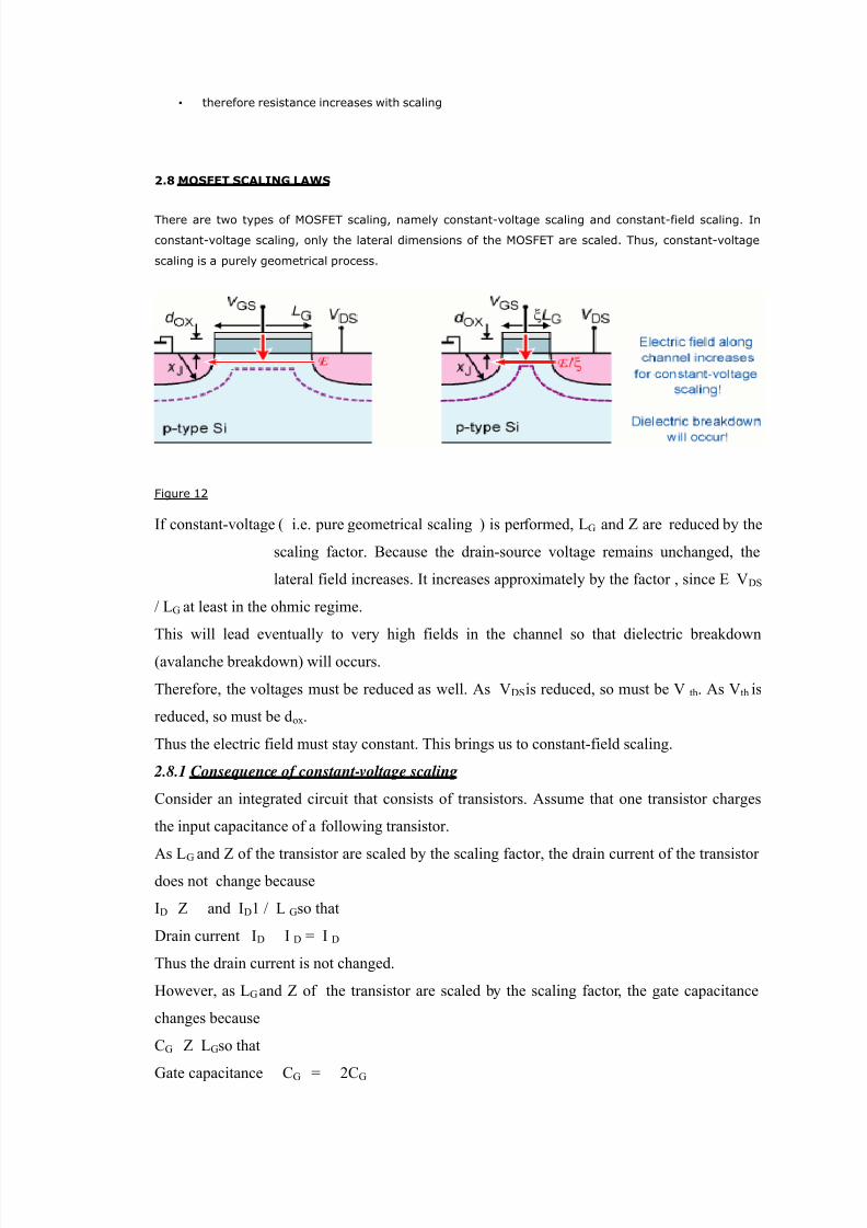
2.8 MOSFET SCALING LAWS
There are two types of MOSFET scaling, namely constant-voltage scaling and constant-field scaling. In
constant-voltage scaling, only the lateral dimensions of the MOSFET are scaled. Thus, constant-voltage
scaling is a purely geometrical process.
Figure 12
If constant-voltage ( i.e. pure geometrical scaling ) is performed, LG and Z are reduced by the
scaling factor. Because the drain-source voltage remains unchanged, the
lateral field increases. It increases approximately by the factor , since E VDS
/ LG at least in the ohmic regime.
This will lead eventually to very high fields in the channel so that dielectric breakdown
(avalanche breakdown) will occurs.
Therefore, the voltages must be reduced as well. As VDS is reduced, so must be Vth. As Vth is
reduced, so must be dox.
Thus the electric field must stay constant. This brings us to constant-field scaling.
2.8.1 Consequence of constant-voltage scaling
Consider an integrated circuit that consists of transistors. Assume that one transistor charges
the input capacitance of a following transistor.
As LG and Z of the transistor are scaled by the scaling factor, the drain current of the transistor does not change because
ID Z and ID 1 / LG so that
Drain current ID ID = ID
Thus the drain current is not changed.
However, as LG and Z of the transistor are scaled by the scaling factor, the gate capacitance
changes because
CG Z LG so that
Gate capacitance CG = 2CG

7/14/2019 Nano
http://slidepdf.com/reader/full/nano55cf9d2d550346d033ac8bf6 21/44
Thus the gate capacitance strongly changes upon scaling.
The time required to charge the gate capacitance with a drain current so that a threshold
voltage Vth is reached, can be derived from the equation
Q = CG Vth.
The time is given by:
T = CG / ( dQ / dt) = CG / ID
Thus the charging time changes according to charging time
t = 2t
As a consequence, scaled integrated circuits can operate at higher frequencies.These factoes
allow one to attain higher clock speed in integrated circuits as they are scaled down.The
following table illustrates performance increase as linewidths shrink.
2.8.2 SUMMARY OF CONSTANT-FIELD AND CONSTANT-VOLTAGE SCALING:
ECE 663
Constant Field Scaling: keep E constant in channel k= λ
Constant Voltage Scaling: keep supply voltage constantk=1(used for submicron scaling)
Parameters Const Field Const Volt
Dimensions 1/λ 1/λ
Potentials 1/λ 1
Doping Concentration λ λ2
Electric Field 1 λ
Current 1/λ λ
Gate Delay 1/λ 1/ λ2
Table 1: Year Linewidth Clockspeed
Beginning of 1970s 10µm 1MHz
End of 1970s 3µm 5MHz
Beginning of 1980s 2µm 20MHz

7/14/2019 Nano
http://slidepdf.com/reader/full/nano55cf9d2d550346d033ac8bf6 22/44
End of 1980s 0.8 µm 50 MHz
Beginning of 1990s 0.5 µm 100MHz
End of 1990s 0.25 µm 750MHz
Beginning of 2000s 0.13 µm 2GHz
Table shows typical line widths and clock speeds versus year.
2.9 Problems Of Scaling: Short-Channel Effects
A MOSFET device is considered to be short when the channel length is the same order of
magnitude as the depletion-layer widths ( xdD, xdS ) of the source and drain junction.
As the channel length L is reduced to increase both the operation speed and the number of
components per chip, the so-called short-channel effects arise.
Chapter 3S hort Channel Effect
I n electronics, a short-channel effect is an effect whereby a MOSFET, in which
the channel length is the same order of magnitude as the depletion-layer widths (xdD, xdS) of the source
and drain junction, behaves differently from other MOSFETs.
As the channel length L is reduced to increase both the operation speed and the number of components
per chip, the so-called short-channel effects arise.
The short-channel effects are attributed to two physical phenomena:
1. The limitation imposed on drift characteristics in the channel,
2. The modification of the threshold voltage due to the shortening channel length.
3.2 Types of Short-Channel Effects
The short-channel effects are attributed to two physical phenomena:
1. the limitation imposed on electron drift characteristics in the channel,

7/14/2019 Nano
http://slidepdf.com/reader/full/nano55cf9d2d550346d033ac8bf6 23/44
2. the modification of the threshold voltage due to the shortening channel length.
In particular five different short-channel effects can be distinguished:
1. Drain-induced barrier lowering and punch through
2. Surface scattering
3. Velocity saturation
4. Impact ionization
5. Hot electrons
3.2.1 Drain-induced barrier lowering and punch through
The expressions for the drain and source junction widths are:
Xdb = {(2c / qNa) (Vds + Qsi + Vsb)}1/2
Xds = {(2c / qNa) (Qsi + Vdb)}1/2
Here Vsb and Vdb are source-to-body and drain-to-body voltages.
When the depletion regions surrounding the drain extends to the source, so that the two
depletion layer merge (i.e., when xdS + xdD = L), punch trough occurs. Punch through can be
minimized with thinner oxides, larger substrate doping, shallower junctions, and obviously
with longer channels. The current flow in the channel depends on creating and sustaining an
inversion layer on the surface. If the gate bias voltage is not sufficient to invert the surface
(VGS<VT0), the carriers (electrons) in the channel face a potential barrier that blocks the flow.
Increasing the gate voltage reduces this potential barrier and, eventually, allows the flow of
carriers under the influence of the channel electric field. In small-geometry MOSFETs, the
potential barrier is controlled by both the gate-to-source voltage VGS and the drain-to-source
voltage VDS . If the drain voltage is increased, the potential barrier in the channel decreases,
leading to drain-induced barrier lowering (DIBL). The reduction of the potential barrier
eventually allows electron flow between the source and the drain, even if the gate-to-source
voltage is lower than the threshold voltage. The channel current that flows under this
conditions (VGS<VT0) is called the sub-threshold current.
3.2.2 Surface scattering
As the channel length becomes smaller due to the lateral extension of the depletion layer into
the channel region, the longitudinal electric field component ey increases, and the surface
mobility becomes field-dependent. Since the carrier transport in a MOSFET is confined within
the narrow Short-Channel Effects in MOSFETs inversion layer, and the surface scattering
(that is the collisions suffered by the electrons that are accelerated toward the interface by ex)
causes reduction of the mobility, the electrons move with great difficulty parallel to the

7/14/2019 Nano
http://slidepdf.com/reader/full/nano55cf9d2d550346d033ac8bf6 24/44
interface, so that the average surface mobility, even for small values of ey, is about half as
much as that of the bulk mobility.
Figure 13
3.2.3 Velocity saturation
The performance short-channel devices are also affected by velocity saturation, which reduces
the trans conductance in the saturation mode. At low ey, the electron drift velocity vde in the
channel varies linearly with the electric field intensity. However, as ey increases above 104
V/cm, the drift velocity tends to increase more slowly, and approaches a saturation value of
vde (sat)=107 cm/s around ey =105 V/cm at 300 K.
Note that the drain current is limited by velocity saturation instead of pinch off. This occurs in
short channel devices when the dimensions are scaled without lowering the bias voltages.
Using vde(sat), the maximum gain possible for a MOSFET can be defined as
m ox de(sat ) g WC v
3.2.4 Impact ionization
Another undesirable short-channel effect, especially in NMOS, occurs due to the high velocity
of electrons in presence of high longitudinal fields that can generate electron-hole (e-h) pairs
by impact ionization, that is, by impacting on silicon atoms and ionizing them. It happens as
follow: normally, most of the electrons are attracted by the drain, while the holes enter the
substrate to form part of the parasitic substrate current. Moreover, the region between the
source and the drain can act like the base of an npn transistor, with the source playing the role
of the emitter and the drain that of the collector. If the aforementioned holes are collected by
the source, and the corresponding hole current creates a voltage drop in the substrate material
of the order of .6V, the normally reversed-biased substrate-source pn junction will conduct
appreciably. Then electrons can be injected from the source to the substrate, similar to the

7/14/2019 Nano
http://slidepdf.com/reader/full/nano55cf9d2d550346d033ac8bf6 25/44
injection of electrons from the emitter to the base. They can gain enough energy as they travel
toward the drain to create new eh pairs. The situation can worsen if some electrons generated
due to high fields escape the drain field to travel into the substrate, thereby affecting other
devices on a chip.
3.2.5 Hot electrons
Another problem, related to high electric fields, is caused by so-called hot electrons. This high
energy electrons can enter the oxide, where they can be trapped, giving rise to oxide charging
that can accumulate with time and degrade the device performance by increasing VT and affect
adversely the gate’s control on the drain current.
Figure 14
The modification of the threshold voltage due to Short-Channel Effects (SCE)
The equation giving the threshold voltage at zero-bias
Vto=Vfb+2Qf+1/Cox{(2Qsi Na (2Qf)+Q/Cox)}1/2
MOSFETs. In fact that equation assumes that the bulk depletion charge is only due to the
electric field created by the gate voltage, while the depletion charge near n+ source and drain
region is actually induced by pn junction band bending. Therefore, the amount of bulk charge
the gate voltage supports is overestimated, leading to a larger VT than the actual value. The
electric flux lines generated by the charge on the MOS capacitor gate electrode terminate on
the induced mobile carriers in the depletion region just under the gate. For short-channel
MOSFETs, on the other hand, some of the field lines originating from the source and the drain
electrodes terminate on charges in the channel region. Thus, less gate voltage is required to
cause inversion. This implies that the fraction of the bulk depletion charge originating from the
pn junction depletion and hence requiring no gate voltage, must be subtracted from the VT
expression.

7/14/2019 Nano
http://slidepdf.com/reader/full/nano55cf9d2d550346d033ac8bf6 26/44
Figure 15
The figure shows the simplified geometry of the gate-induced bulk depletion region and the p-n junction depletion regions in a short channel MOS transistor. Note that the bulk depletion
region is assumed to have and asymmetric trapezoidal shape, instead of a rectangular shape, to
represent accurately the gate-induced charge. The drain depletion region is expected to be
larger than the source depletion region because the positive drain-to-source voltage reversed-
biases the drain substrate junction. We recognize that a significant portion of the total depletion
region charge under the gate is actually due to the source and drain junction depletion, rather
than the bulk depletion induced by the gate voltage. Since the bulk depletion charge in the
short channel device is smaller than expected, the threshold voltage expression must bemodified to account for this reduction:
T 0 (short channel) T 0 T 0 V
V V ,
Where VT0 is the zero-bias threshold
voltage calculated using the conventional
long-channel formula and DVT0 is the
threshold voltage shift (reduction) due to
the short-channel effect. The reduction
term actually represents the
amount of charge differential between a
rectangular depletion region and a
trapezoidal depletion region.
Let DLS and DLD represent the lateral
extent of the depletion regions associated with the source junction and the drain junction,
respectively. Then, the bulk depletion region charge contained
To calculate DLS and DLD, we will use the simplified geometry shown in the figure.

7/14/2019 Nano
http://slidepdf.com/reader/full/nano55cf9d2d550346d033ac8bf6 27/44
Here, xdS and xdD represent the depth of the pn-junction depletion regions associated with the
source and the drain, respectively. The edges of the source and drain diffusion regions are
represented by, each with a radius equal to the junction depth, xj. The vertical extent of the
bulk depletion region into the substrate is represented by xdm.
The Threshold Voltage Equation is-
<>Vto=1/Cox(2 q Na 2 Qf) X/2L [{1+(2Xdb/x)-1}1/2 + {(2Xds/X)+1}1/2]
VT0= V’T0 + (q NI)/Cox = 0.855 V.
Next, the amount of the threshold voltage reduction due to short-channel effects must be
calculated.
The source and drain junction built-in voltage is
F0= (kT/q) ln((ND NA)/ ni 2)= 0.76 V
Chapter
4S imulation of nano scaled n-mos device
O ur main work is to design and simulate nMOS of gate length 0.18µm using
TCAD which is basically simulation device named ATLAS. But ATLAS is the hardware
simulation. We need a process simulation method first. That is ATHENA.

7/14/2019 Nano
http://slidepdf.com/reader/full/nano55cf9d2d550346d033ac8bf6 28/44
4.1 PROCESS SIMULATION :
Process simulation involves the modeling of physical processes with the aim of studying their
effects on the external environment and the objects they are applied to. These processes usually
involve the interaction between two or more systems. Process simulation comprises the
modeling of all process steps which are necessary for the fabrication of semiconductor devices.
These process steps, are layer deposition, lithography, etching, implantation, oxidation and
diffusion. Physically and/or empirically based models are applied in the simulation. The
process simulation uses Athena as a simulator that provides general capabilities for numerical,
physically-based, two-dimensional simulation of semiconductor processing. In process
simulation, the result of an implantation step is mostly described by a so-called Pearson
function whereas the diffusion equation is solved to derive the influence of an annealing step.
Figure- illustrates the overview of process simulation.
Figure 16
4.2 Fabrication Process in ATHENA: -Start ATHENA by typing “go athena”.
“go athena”
The first step in simulating a device is defining a grid. This is a very important step because it
will determine the accuracy and time of the simulation. To access the grid GUI (graphical user
interface) in DECKBUILD open the Commands menu and select Mesh Define. It is necessary
that both “X” and “Y” locations are specified.

7/14/2019 Nano
http://slidepdf.com/reader/full/nano55cf9d2d550346d033ac8bf6 29/44
4.2.1 Defining initial grid:-
An initial grid has to be specified before any further steps of the design. The Correct
specification of a grid is critical in process simulation. The number of nodes in the grid Np has
a direct influence on simulation accuracy and time. A finer grid should exist in those areas of
the simulation structure where ion implantation will occur, where p-n junction will be formed,
or where optical illumination will change photoactive component concentration
mesh space.mult=1.0
#
x.mesh loc=0.00 spac=0.50
x.mesh loc=0.1 spac=0.02
x.mesh loc=0.38 spac=0.1
x.mesh loc=0.69 spac=0.02
x.mesh loc=0.76 spac=0.5
#
y.mesh loc=-0.017 spac=0.02
y.mesh loc=0.00 spac=0.005
y.mesh loc=0.1 spac=0.02
y.mesh loc=0.2 spac=0.01
y.mesh loc=0.6 spac=0.25
#

7/14/2019 Nano
http://slidepdf.com/reader/full/nano55cf9d2d550346d033ac8bf6 30/44
Figure 17:MESH DEFINED MOS STRUCETUR
Conformal deposition can be used to generate multi-layered structures. Conformal deposition is
the simplest deposit model and can be used in all cases when the exact shape of the deposited layer
is not critical. Conformal deposition can also be used in place of oxidation of planar or quasi-planar
semiconductor regions when doping redistribution during the oxidation process is negligible.A
smooth layer of SiO2 is then deposited on the substrate. The simplest deposit method in
ATHENA is conformal deposition
#
diffus time=30 temp=1000 dryo2 press=1.00 hcl=3
#
etch oxide thick=0.02
4.2.2 ATHENA Deposit Code:
The Geometrical etch is the default method. Deposition and Wet/Dry Etching using the Physical Models in
ATHENA. This example will use a polysilicon gate edge at x=0.3 and set the center of the gate at x=0.0 for the
initial grid. Therefore, polysilicon should be etched to the right from x=0.3. To do so, select Right from the
Geometrical type, and set the Etch location to 0.3. This will give the following statement:
# POLY DEFINITION
ETCH POLY RIGHT P1.X=0.3
The next step in the development is implantation of Boron to create a p-well (excess holes) in
the substrate.

7/14/2019 Nano
http://slidepdf.com/reader/full/nano55cf9d2d550346d033ac8bf6 31/44
4.2.3 Vt Adjust Implant Code:
Boron is then implanted through the gate oxide in a similar fashion as the previous p-well
implant was performed. The code written to the input deck is displayed in below-
#vt adjust implant
implant boron dose=9.5e11 energy=10 pearson
#
This Boron implant acts to define the threshold voltage of this device. The threshold voltage
depending on the dose of the Boron. Higher dose of boron increasing the threshold voltage.
4.2.4 Heavy Drain/Source Doping Code:
The heavy drain/source can then be implanted in the same fashion as the light drain/source.
This heavily doped region is several orders of magnitude greater than the lightly doped region.
This heavy drain/source region is also implanted with Arsenic instead of Phosphorus in the
case of the light drain/source. The implantation code is shown below-
#
implant arsenic dose=5.0e15 energy=50 pearson
#

7/14/2019 Nano
http://slidepdf.com/reader/full/nano55cf9d2d550346d033ac8bf6 32/44
Figure 18
This tutorial process simulation has been building one half of a structure. At some point in the simulation, will
need to obtain the full structure. This must be done before exporting the structure to a device simulator or setting
electrode names. In general, structure reflection should be performed when the structure ceases to be symmetrical
(e.g., a tilted implant, an asymmetrical etching, or a deposition takes place), or when a reflecting boundary
condition no longer applies to the side, which is going to be the center of the structure.
This example will explain how to mirror the structure at its left boundary. To mirror the structure,
select Structure→ Mirror in the Commands menu (Figure -below).
Figure 19
To write the following statement to the input file:
#
STRUCT MIRROR LEFT
#

7/14/2019 Nano
http://slidepdf.com/reader/full/nano55cf9d2d550346d033ac8bf6 33/44
The left half of the structure is a complete mirror copy of the right part, including node
coordinates, doping values, and so on. Beware of rounding errors when mirroring. If the boundary
of reflection is not smooth to within 0.1 angstroms, some points will be duplicated.
4.2.5 Specification of Electrodes in ATHENA: -
The ultimate goal of an simulation is usually to create a device structure (material layers plus doping), which then
can be used by a device simulator (usually for electrical characterization. Although is able to specify the locations
of electrodes, in many cases specifying electrodes must be done in . For example, it is impossible to specify an
electrode location in when the electrode does not consist of straight segments. Also, when specifying electrodes in
, it is useful to transfer electrode layer information from layout to electrical tests in a device simulator can
attribute an electrode to any metal, silicide, or polysilicon region. A special case is the backside electrode, which
can be placed at the bottom of the structure without having a metal region there. If we deposit 0.1 µm aluminum
layer on the full structure after reflection using:
#
DEPOSIT ALUMIN THICK=0.1
#
and etched the following part of the layer between x=-0.8 and x=0.8, using the Any Shape specification in the
Athena Etch Menu
#
ETCH ALUMINUM START X=-0.8 Y=-20
ETCH CONT X=-0.8 Y=20
ETCH CONT X=0.8 Y=20
ETCH DONE X=0.8 Y=-20
#
The following statement will for defining the source electrode:
#
ELECTRODE NAME=SOURCE X=-0.9
#
Similarly, specify the drain electrode:
#
ELECTRODE NAME=DRAIN X=0.9
#
The polysilicon gate electrode specification has the same format. For this structure it can be done the same way as
for source or drain:
#

7/14/2019 Nano
http://slidepdf.com/reader/full/nano55cf9d2d550346d033ac8bf6 34/44
ELECTRODE NAME=GATE X=0.0
#
If the polysilicon layer is not the topmost
layer at x=0, the Y Position
Figure 20
can be specified.
In this case, check the Y Position
checkbox and type in a y coordinate within
the polygate layer (e.g., -0.2). If Y is not
specified and the electrode is not on top,
will look for the electrode in the underlying
layers. If it fails, an error will be reported. To specify a backside electrode, select Backside from the Electrode
Type field and type in a name ATHENA.
The following backside electrode statement will appear in the input file:
#
ELECTRODE NAME=BACK BACKSIDE
#
Figure 21
4.3 ATLAS:
y ATLAS is a 2D and 3D Device Simulation Framework
y ATLAS solves the fundamental physical equations describing the
y dynamics of carriers in semiconductor devices for arbitrary device
y structures

7/14/2019 Nano
http://slidepdf.com/reader/full/nano55cf9d2d550346d033ac8bf6 35/44
y ATLAS predicts terminal characteristics of semiconductor devices
y for steady state, transient, and small signal AC stimuli
y ATLAS gives insight into the internal characteristics of
y Semiconductor devices (e.g. carrier densities, fields, ionization/ recombination rates,
current density etc.)
4 .3 .1 E lements of AT L AS I nput D eck :
y Group Statements
1. Structure Specification MESH
REGION
ELECTRODE
DOPING
2. Material Models Specification MATERIAL
MODELS
CONTACT
INTERFACE
3. Numerical Models Specification METHOD
4. Solution Specification LOG
SOLVE
LOAD
5. Results Analysis SAVE
EXTRACTTONYPLOT
4.3.2 ATLAS INPUT AND OUTPUT:
The following diagram shows the input output technique of ATLAS simulator.

7/14/2019 Nano
http://slidepdf.com/reader/full/nano55cf9d2d550346d033ac8bf6 36/44
Figure 22
4.4 P r oject P r ogr ammin g
NMOS GATE LENGTH-0.18 um
go Athena
# Grid definition for x and y axis (NMOS)
line x loc=0.15 spac=0.1
line x loc=0.2 spac=0.006
line x loc=0.4 spac=0.006
line x loc=0.6 spac=0.01

7/14/2019 Nano
http://slidepdf.com/reader/full/nano55cf9d2d550346d033ac8bf6 37/44
line y loc=0.0 spac=0.002
line y loc=0.2 spac=0.005
line y loc=0.5 spac=0.05
line y loc=0.8 spac=0.15
# Defining the initial substrate doping for NMOS, p-type with boron doping
init orientation=100 c.boron=1.0e15 space.mul=2
# Performing oxidation and pwell formation including masking off of the nwell (NMOS)
diffus time=30 temp=1000 dryo2 press=1.00 hcl=3 etch oxide thick=0.02
#P-well Implant (NMOS)
implant boron dose=3.0e13 energy=200 pearson diffus temp=950 time=100 weto2 hcl=3
# Sacrificial "cleaning" oxide (NMOS)
diffus time=20 temp=1000 dryo2 press=1 hcl=3 etch oxide all
#gate oxide (NMOS)
diffus time=3 temp=895 dryo2 press=1.00 hcl=1
# vt adjust implant (NMOS)
implant boron dose=1.5e13 energy=45 pearson
#performing conformal deposition (NMOS)
depo poly thick=0.2 divi=10 etch poly left p1.x=0.51
# Polysilicon oxidation (NMOS)method fermi compress
diffuse time=5 temp=900 weto press=0.8
#polysilicon doping/Light doped drain extension
implant arsenic dose=1.0e15 energy=30 pearson
# p-doped halo implant (NMOS)
implant boron dose=3.0e13 energy=15 tilt=30 fullrotat

7/14/2019 Nano
http://slidepdf.com/reader/full/nano55cf9d2d550346d033ac8bf6 38/44
# Spacer oxide deposition (NMOS)
depo oxide thick=0.10 divisions=8 etch oxide dry thick=0.10
# Source/drain implant (NMOS)
implant arsenic dose=5e15 energy=60 pearson
For NMOS
# Rapid Thermal Annealing method fermi compress
diffuse time=1 temp=1000 nitro press=1.0
# Pattern s/d contact metal
etch oxide left p1.x=0.35 deposit alumin thick=0.03 divi=2 etch alumin right p1.x=0.33
# Mirror the structure
structure mirror right
#Specifications of electrodes
electrode name=gate x=0.59 y=0.1
electrode name=source x=0.2
electrode name=drain x=1.0
electrode name=substrate backside
#structure outfile=nmos_0.str
structure outfile=mos1ex04_0.str
# plot the structure
tonyplot mos1ex04_0.str -set mos1ex04_0.set
# DIBL test for NMOS
go atlas
# set material models
models cvt srh print
contact name=gate n.poly
interface qf=3e10
# get initial solution
solve init

7/14/2019 Nano
http://slidepdf.com/reader/full/nano55cf9d2d550346d033ac8bf6 39/44
method newton trap
solve prev
# Bias the drain a bit...
solve vdrain=0.025 vstep=0.025 vfinal=0.05 name=drain
solve vdrain=0.05 vstep=0.025 vfinal=0.1 name=drain
# Ramp the gate
log outf=nmos_1.log master
solve vgate=0 vstep=0.1 vdrain=0.1 vfinal=1.0 name=gate
solve vgate=1.0 vstep=0.1 vdrain=0.1 vfinal=1.5 name=gate compl=1.1e-7
cname=drain
# extract device parameters
extract init inf="nmos_1.log"
extract name="nvt1" x.val from curve(abs(v."gate"),abs(i."drain")) where y.val=0.1e-6
log off
# Now start again and ramp the drain to 2 volts...
solve init
# Bias the drain to 2 volts......slowly at first....
solve vdrain=0.025 vstep=0.025 vfinal=0.1 name=drain
solve vdrain=0.1 vstep=0.25 vfinal=1.0 name=drain
# Ramp the gate again with another opened logfile...
log outf=nmos_2.log master
solve vgate=0 vstep=0.1 vdrain=1.0 vfinal=1.0 name=gate
solve vgate=1.0 vstep=0.1 vdrain=1.0 vfinal=1.5 name=gate compl=1.1e-7
cname=drain
# extract the next device parameter with the drain now at 2 volts....
extract init inf="nmos_2.log"
extract name="nvt2" x.val from curve(abs(v."gate"),abs(i."drain")) where y.val=0.1e-6
log off
# Now start again and ramp the drain to 2 volts...
solve init
# Bias the drain to 2 volts......slowly at first....
solve vdrain=0.025 vstep=0.025 vfinal=0.1 name=drain
solve vdrain=0.1 vstep=0.25 vfinal=2.0 name=drain
# Ramp the gate again with another opened logfile...
log outf=nmos_3.log master

7/14/2019 Nano
http://slidepdf.com/reader/full/nano55cf9d2d550346d033ac8bf6 40/44
solve vgate=0 vstep=0.1 vdrain=2.0 vfinal=1.0 name=gate
solve vgate=1.0 vstep=0.1 vdrain=2.0 vfinal=1.5 name=gate compl=1.1e-7
cname=drain
# extract the next device parameter with the drain now at 2 volts....
extract init inf="nmos_3.log"
extract name="nvt3" x.val from curve(abs(v."gate"),abs(i."drain")) where y.val=0.1e-6
# Calcate a DIBL parameter....in V/V
extract name="ndibl" ($"nvt1"-$"nvt2")/(1.0-0.1)
tonyplot -overlay nmos_1.log nmos_2.log nmos_3.log
quit
4.5 Improvement and results after simulation of NMOS:
The NMOS is improved to 0.18 um gate length after overcome those upper mentioned
problems regarding scaling of MOSFET. We are able to make a software simulation of 0.18
um gate lengthed NMOS which can produce the same output and take a very less amount of
power required.
Figure 23
The basic structure of 0.18 um scaled nmos.

7/14/2019 Nano
http://slidepdf.com/reader/full/nano55cf9d2d550346d033ac8bf6 41/44
Figure 24: drain current Vs Gate Voltage plot
The above graph shows that how a 0.18um scaled nmos acts according to drain current againstthe gate applied voltage.
Figure 25: drain current Vs drain voltage curve
The above plot is showing how reacts the nmos according to drain current against drainvoltage.

7/14/2019 Nano
http://slidepdf.com/reader/full/nano55cf9d2d550346d033ac8bf6 42/44
Figure 26: Plot of DIBL characteristics of nmos
The above curve shows the output in case of Drain-induced barrier lowering (DIBL) for 0.18um scaled nmos.
R E F E R E N C E
1. MOSFET Modeling for VLSI Simulation Theory And Practice – by Narain Arora
2. www.ecse.rpi.edu 3. en.wikipedia.org/wiki/MOSFET 4. www.zettaflops.org/fec05/Peter-Zeitzoff.pp 5. www.cs.ucl.ac.uk/staff/ucacdxq/projects/vlsi/report.pd 6. en.wikipedia.org/wiki/Short-channel _effect
7. iopscience.iop.org/1402-4896/24/2/016/pdf/physscr_24_2_016.pdf

7/14/2019 Nano
http://slidepdf.com/reader/full/nano55cf9d2d550346d033ac8bf6 43/44
L ist O f Avvr ebiat ion
ATLAS, ATHENA
Buried OXide (BOX)BJT -bipolar junction transistor
C D = capacitance of the depletion layer and C OX = capacitance of the oxide layer
DVT0 is the threshold voltage shift (reduction),MOS’ -Metal Oxide Semiconductor
MOSFET-Metal–oxide–semiconductor field-effect transistor nMOS, pMOS -n- type or p-type MOS,FET- field effect transistor ,MISFET - metal–insulator–semiconductor FET.
JFET –junction field effecy transistor,silicon dioxide (SiO2) ,V GB
Silicon On Insulator SOI,Ultra Thin Channel (UTC)
SEMiconductor. On Insulator (SEMOI)
Raised Source/ Drain (RSD)
V th is the threshold voltage
ULSI (ultra large scale integration)
IC intregation circuit
Vsb and Vdb -source-to-body and drain-to-body voltagesgate-to-source voltage VGS and the drain-to-source voltage VDS drain-induced barrier lowering (DIBL)VT0) -sub-threshold voltage
F0-source and drain junction built-in voltage
GUI (graphical user interface)
TCAD
GUI (graphical user interface)fromSILVACO
SOI

7/14/2019 Nano
http://slidepdf.com/reader/full/nano55cf9d2d550346d033ac8bf6 44/44
C O N C L U S I O N
Process and device simulation, modeling and parameter extraction for FD
& PD MOSFETs have been performed using ATHENA and ATLAS simulation
framework from SILVACO. Threshold voltage performance, sub threshold slope,
Id-Vg characteristics, leakage current, lattice heating effects and studied to
investigate the comparative performance of FD & PD SOI MOSFET structure. It
was found that FD SOI structure has some advantage over PD SOI structure as
long as the channel front interface potential is significantly higher then channel
back interface potential. Channel back interface potential is mostly controlled by
high fringing fielding in SOI structure. This fringing field related DIBL effectscan be reduced if oxide of lower dielectric material is used in the BOX.
Replacing the BOX with air resulted in a structure known as SON structure.
Analytical expressions for threshold voltage and sub-threshold slope of SON
MOSFTE have been derived and effects of using different materials in GOX and
BOX layers are analyzed. Simulated results show that the SON structure
remarkably reduces SCEs related device performance degradation like threshold
voltage roll-off and higher sub threshold slope. Present study demonstrates that
SON-MOSFET technology is able to offer devices with high performance under
different short channel conditions. Analytical model for SON structure presented
here can be incorporated in the future simulation software.