
MULTISTAGE AMPLIFIERS. Multistage Amplifiers Two or more amplifiers can be connected to increase the...
22
MULTISTAGE AMPLIFIERS
-
Upload
maribel-bridgman -
Category
Documents
-
view
235 -
download
1
Transcript of MULTISTAGE AMPLIFIERS. Multistage Amplifiers Two or more amplifiers can be connected to increase the...

MULTISTAGE AMPLIFIERS

Multistage Amplifiers
Two or more amplifiers can be connected to increase the gain of an ac signal. The overall gain can be calculated by simply multiplying each gain together.
A’v = Av1Av2Av3 ……
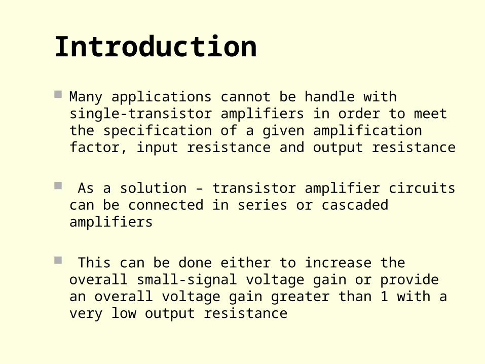
Introduction
Many applications cannot be handle with single-transistor amplifiers in order to meet the specification of a given amplification factor, input resistance and output resistance
As a solution – transistor amplifier circuits can be connected in series or cascaded amplifiers
This can be done either to increase the overall small-signal voltage gain or provide an overall voltage gain greater than 1 with a very low output resistance

Multistage Amplifiers
Multi-stage amplifiers are amplifier circuits cascaded to increased gain. We can express gain in decibels(dB).
Two or more amplifiers can be connected to increase the gain of an ac signal. The overall gain can be calculated by simply multiplying each gain together.
A’v = Av1Av2Av3 ……
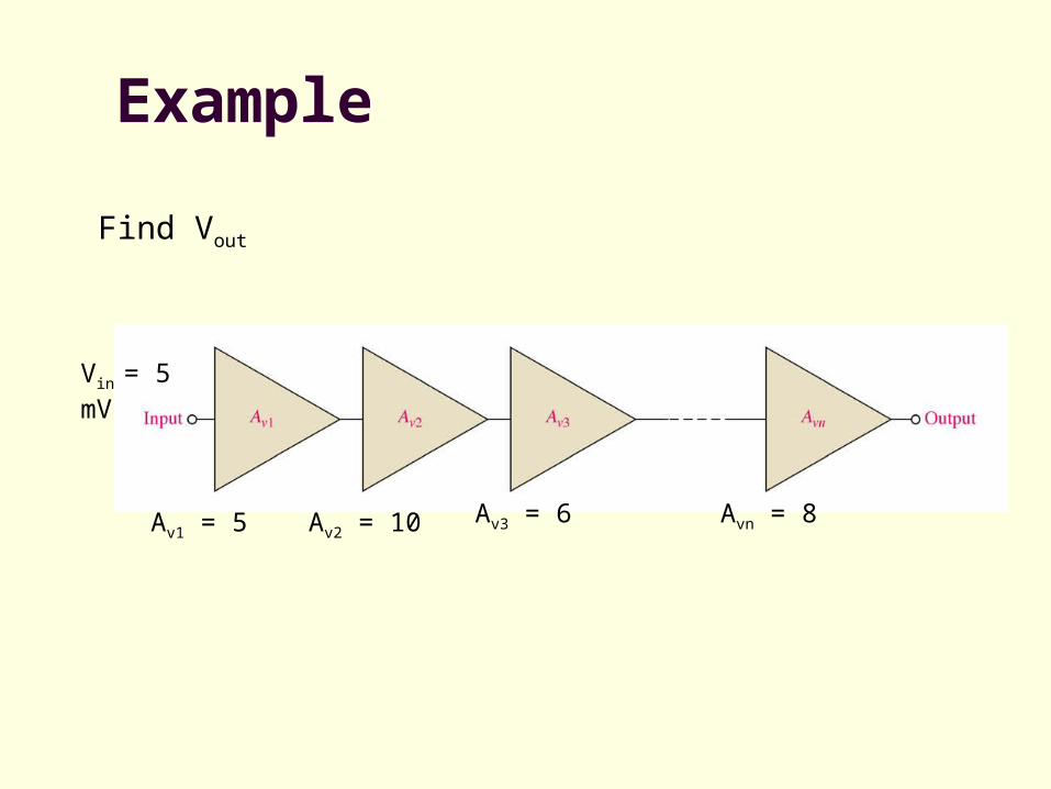
Example
Find Vout
Av1 = 5 Av2 = 10 Av3 = 6 Avn = 8
Vin = 5 mV
6
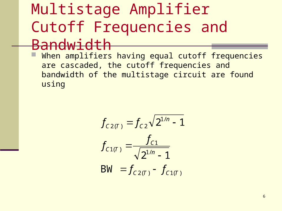
Multistage Amplifier Cutoff Frequencies and Bandwidth When amplifiers having equal cutoff frequencies are cascaded,
the cutoff frequencies and bandwidth of the multistage circuit are found using
)(1)(2
/1
1)(1
/12)(2
BW12
12
TCTC
n
CTC
nCTC
ff
ff
ff

Introduction (cont.) Multistage amplifier configuration:
Rc1 Rc2RB
Vi Q1
Q2R2
RL
R1Vo
Vi Q1
Q2
R3
R1 R2
Vi
Vo
R1
Vi
Vo
T
Cascade /RC coupling
Cascode
Transformer coupling Darlington/Direct coupling
Q1
Q2
Q1
Q2

i) Cascade Connection-The most widely used method-Coupling a signal from one stage to the anotherstage and block dc voltage from one stage tothe another stage-The signal developed across the collectorresistor of each stage is coupled intothe base of the next stage -The overall gain = product of the individual gain
**refer page 219

i) Cascade Connection (cont.) small signal gain is: by determine the voltage gain at stages 1 & stage 2
therefore
- the gain in dB
input resistance
Output resistance - assume ,so also
Therefore
))(//)(//( 22121Si
iLCCmm
S
oV RR
RRRrRgg
V
VA
121 //// rRRRis
0SV 021 VV 0211 VgVg mm
20 CRR
21 VVV AAA
)log(20)( VdBV AA
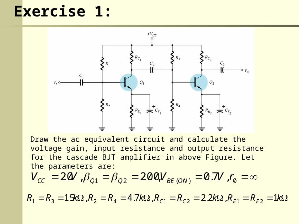
Exercise 1:
Draw the ac equivalent circuit and calculate the voltage gain, input resistance and output resistance for the cascade BJT amplifier in above Figure. Let the parameters are:
kRRkRRkRRkRR EECC 1,2.2,7.4,15 21214231
0)(21 ,7.0,200,20 rVVVV ONBEQQCC

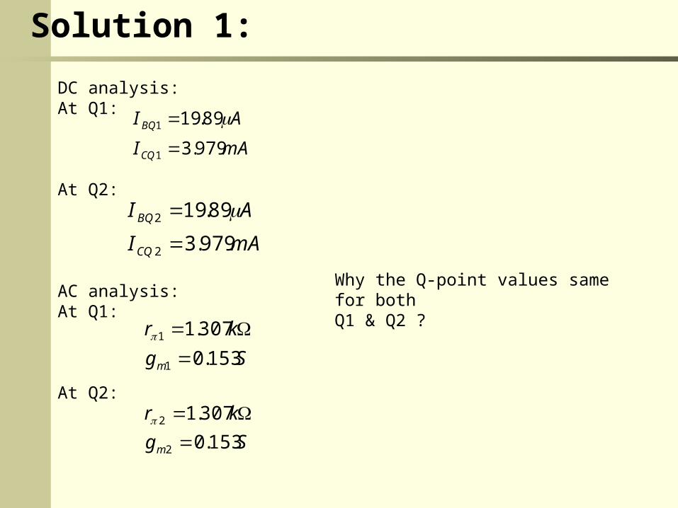
Solution 1 (cont.):
21
1
// RR
RB
1r
1V
2V 2r2CR1CR
11 Vgm22 Vgm43
2
// RR
RB
iV0V
1B 2B
1E
1C
2E
2CiR
0R
Ac equivalent circuit for cascade amplifier
Solution 1:
DC analysis:At Q1:
At Q2:
AC analysis:At Q1:
At Q2:
Sg
kr
m 153.0
307.1
1
1
Why the Q-point values same for bothQ1 & Q2 ?
mAI
AI
CQ
BQ
979.3
89.19
1
1
Sg
kr
m 153.0
307.1
2
2
mAI
AI
CQ
BQ
979.3
89.19
2
2
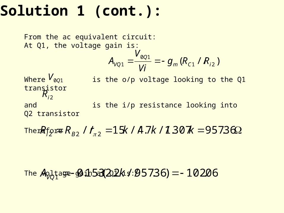
Solution 1 (cont.):
From the ac equivalent circuit:At Q1, the voltage gain is:
Where is the o/p voltage looking to the Q1 transistor
and is the i/p resistance looking into Q2 transistor
Therefore
The voltage gain at Q1 is:
2iR
10QV
)//( 2110
1 iCmQ
VQ RRgVi
VA
06.102)36.957//2.2(153.01 kAVQ
36.957307.1//7.4//15// 222 kkkrRR Bi

Solution 1 (cont.):
From the ac equivalent circuit:At Q2, the voltage gain is:
Where is the i/p voltage looking into the Q2 transistor
Therefore, the voltage gain at Q2 is:
The overall gain is then,
** The large overall gain can be produced by multistage amplifiers!!So, the main function of cascade stage is to provided the larger overall gain
2iQV
)( 22
02 Cm
iQVQ Rg
V
VA
6.336)2.2(153.02 kAVQ
353,34)6.336)(06.102(21 VQVQV AAA

Solution 1 (cont.):
From the ac equivalent circuit:
The i/p resistance is:
The o/p resistance is:
36.957
307.1//7.4//15//// 121 kkkrRRRi
kRR Co 2.22
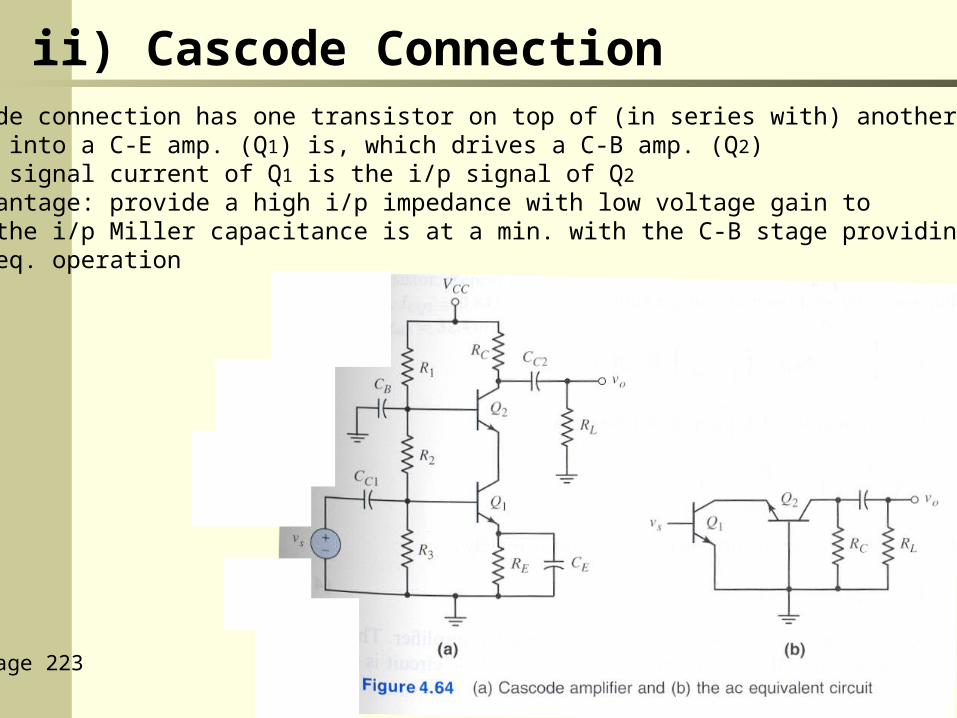
ii) Cascode Connection-A cascode connection has one transistor on top of (in series with) another-The i/p into a C-E amp. (Q1) is, which drives a C-B amp. (Q2)-The o/p signal current of Q1 is the i/p signal of Q2
-The advantage: provide a high i/p impedance with low voltage gain to ensure the i/p Miller capacitance is at a min. with the C-B stage providing good high freq. operation
**refer page 223

ii) Cascode Connection (cont.)
From the small equivalent circuit, since the capacitors act as short circuit,by KCL equation at E2:
solving for voltage
Where
the output voltage is
or
222
211
Vg
r
VVg mm
2V
SmVgr
V 12
22 1
222 rgm
)//)(( 22 LCmo RRVgV
SLCmmo VRRr
ggV )//1 2
221
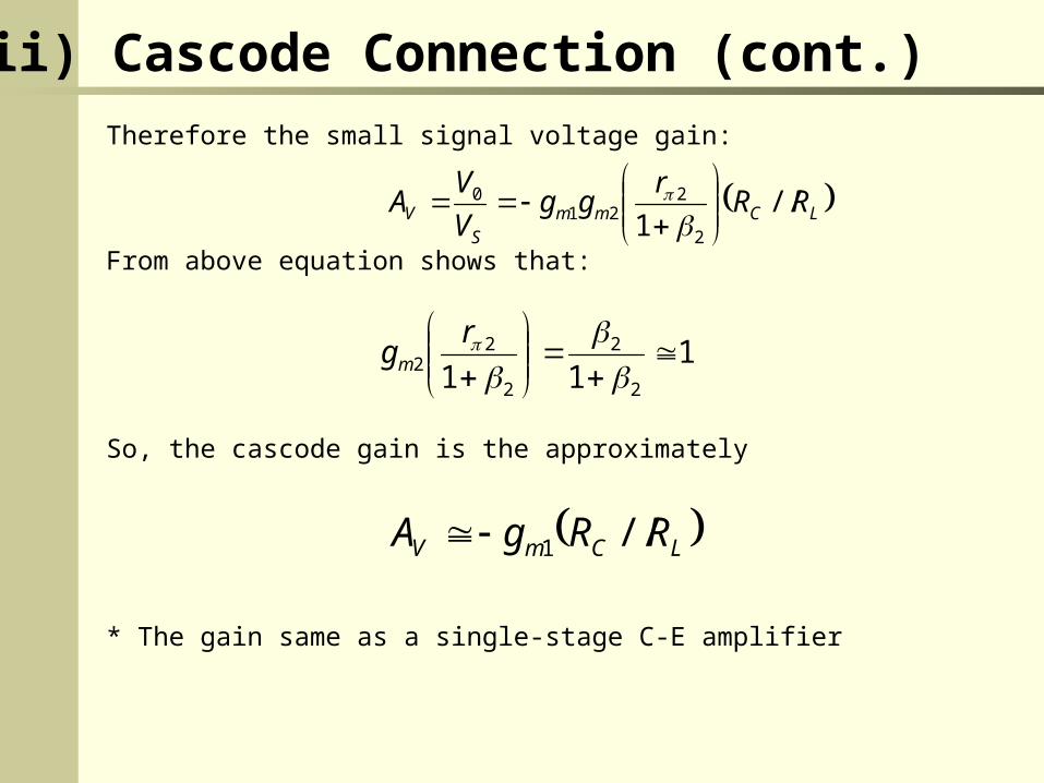
ii) Cascode Connection (cont.)
Therefore the small signal voltage gain:
From above equation shows that:
So, the cascode gain is the approximately
* The gain same as a single-stage C-E amplifier
LCmmS
V RRr
ggV
VA //
1 2
221
0
LCmV RRgA //1
111 2
2
2
22
rgm

iii) Darlington Connection-The main feature is that the composite transistor acts as a single unit with a current gain that is the product of the current gains of the individual transistors-Provide high current gain than a single BJT-The connection is made using two separate transistors having current gains of and
So, the current gain
If
The Darlington connection provides a current gain of
21 D
1 2
21
2 D
Figure 1: Darlington transistor

iii) Darlington Connection (cont.) Figure shown a Darlington configuration
refer page 222

iii) Darlington Connection (cont.) The small current gain :
Since
Therefore
Then,
The o/p current is:
The overall gain is:
** The overall small-signal current gain = the product of the individual current gains
iimm IIrgVg 11111
212 )( rIIV ii
iimm IIVgVgI )1( 12122110
211210 )1( i
i I
IA
ioi IIA /
11 rIV i
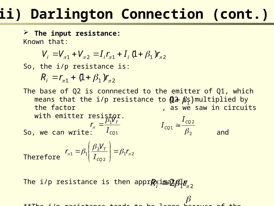
iii) Darlington Connection (cont.)
The input resistance:Known that:
So, the i/p resistance is:
The base of Q2 is connnected to the emitter of Q1, which means that the i/p resistance to Q2 is multiplied by the factor , as we saw in circuits with emitter resistor.
So, we can write: and
Therefore
The i/p resistance is then approximately
**The i/p resistance tends to be large because of the multiplication
21121 )1( rIrIVVV iii
211 )1( rrRi
1
1
CQ
T
I
Vr
2
21
CQCQ
II
212
211 rI
Vr
CQ
T
212 rRi
)1( 1