Multiple-engineering controlled growth of tunable-bandgap ...
8
Multiple-engineering controlled growth of tunable-bandgap perovskite nanowires for high performance photodetectors† Kuankuan Ren, ab Jian Wang, c Kong Liu, ab Yanbin Huang, ab Yang Sun, ab Muhammad Azam, ab Peng Jin, c Zhijie Wang, * ab Shengchun Qu * ab and Zhanguo Wang ab Controllable growth of perovskite nanowires is very important for various applications in optical and electrical devices. Although significant progress has been achieved in the solution method, a deep understanding of the mechanics of growing perovskite nanowires is still lacking. Herein, we developed an electrochemical method for growing the perovskite nanowires and studied the growth processes systematically. The initial nucleation and crystal growth could be controlled by simply varying the additive solvents, thus leading to two stable size ratio distributions of the perovskite nanowires. Further, with compositional engineering, the bandgap of the perovskites could be tuned from 1.59 eV to 3.04 eV. All the as-grown perovskite nanowires displayed a unique structure with high crystallization quality, contributing to a very high responsivity of 2.1 A W 1 and a large on/off ratio of 5 10 3 for the photodetectors based on the CH 3 NH 3 PbBr 3 nanowires. All of these findings demonstrate that the optimized solution method offers a new approach to synthesize perovskite nanowires for applications in photoelectric devices. Hybrid organic–inorganic perovskite materials have changed the existing landscape in photovoltaic research owing to their exceptional optoelectronic performance parameters, such as long carrier lifetimes, long carrier diffusion lengths, high absorption coefficient and high carrier mobility. 1–5 These fascinating properties boosted the latest certied power conversion efficiency of the perovskite solar cells up to 23.7%, inspiring researchers greatly to develop applications for perov- skite devices. 6,7 Therefore, abundant studies explored the applications of perovskite light emitting diodes (LED), lasers and photodetectors. 8–13 Most of these devices are primarily based on polycrystalline perovskite thin lms, single crystals or nanomaterials. Particularly, the perovskite nanomaterials have become a new research eld for optoelectronic applications due to their unique morphologies and extraordinary performances. The corresponding perovskite nanodevices display outstanding quantum yields, high photosensitivity, photoelectric conversion efficiency and long-term stability, 14–17 surpassing those of orig- inal material systems. Therein, perovskites nanowires, as the building blocks of optoelectronic integrated devices, have aroused extensive research interests due to their well-dened structures. 18–21 The properties of the nanowires are highly dependent on growth techniques. Up to now, various fabrication technologies have been developed for growing perovskite nanowires, including chemical vapor deposition 22–24 and template-assisted synthesis methods, 25–27 which are based on high temperature processes or extra template assistance. However, perovskite nanowires can be converted directly from the perovskite thin lms or supersaturated perovskite precursor solutions by evaporating the additional solvent without any template in easy- controlled solution methods. 28–31 Although their corresponding devices show promising performances, the nanowires seem to show rough surfaces or large boundaries that limit further performance improvement. There is also an optional solution method, where the perovskite nanowires can be grown by reacting lead acetate (PbAc 2 ) or lead halide (PbX 2 ,X ¼ I, Br, Cl) thin lms with methylammonium halides (CH 3 NH 3 Y, Y ¼ I, Br, Cl) in isopropanol solution. 8,32,33 These nanowires exhibited smooth surfaces and high crystallinity. Nevertheless, most of these studies focus only on one kind of halide perovskite growth. Even other halide perovskites can be transformed by ion-exchange reactions, which also suffer from poor a Key Laboratory of Semiconductor Materials Science, Beijing Key Laboratory of Low Dimensional Semiconductor Materials and Devices, Institute of Semiconductors, Chinese Academy of Sciences, Beijing, 100083, China. E-mail: [email protected]; [email protected] b Center of Materials Science and Optoelectronics Engineering, University of Chinese Academy of Sciences, Beijing 100049, China c Research Center of Ultra-Precision Optoelectronic Instrument, Harbin Institute of Technology, Harbin 150080, China † Electronic supplementary information (ESI) available: Materials and methods, additional gures and discussions. See DOI: 10.1039/c9ra01689a Cite this: RSC Adv. , 2019, 9, 19772 Received 6th March 2019 Accepted 28th May 2019 DOI: 10.1039/c9ra01689a rsc.li/rsc-advances 19772 | RSC Adv. , 2019, 9, 19772–19779 This journal is © The Royal Society of Chemistry 2019 RSC Advances PAPER Open Access Article. Published on 25 June 2019. Downloaded on 12/14/2021 6:19:37 PM. This article is licensed under a Creative Commons Attribution-NonCommercial 3.0 Unported Licence. View Article Online View Journal | View Issue
Transcript of Multiple-engineering controlled growth of tunable-bandgap ...

RSC Advances
PAPER
Ope
n A
cces
s A
rtic
le. P
ublis
hed
on 2
5 Ju
ne 2
019.
Dow
nloa
ded
on 1
2/14
/202
1 6:
19:3
7 PM
. T
his
artic
le is
lice
nsed
und
er a
Cre
ativ
e C
omm
ons
Attr
ibut
ion-
Non
Com
mer
cial
3.0
Unp
orte
d L
icen
ce.
View Article OnlineView Journal | View Issue
Multiple-enginee
aKey Laboratory of Semiconductor Material
Dimensional Semiconductor Materials an
Chinese Academy of Sciences, Beijing, 100
[email protected] of Materials Science and Optoelectr
Academy of Sciences, Beijing 100049, ChinacResearch Center of Ultra-Precision Optoel
Technology, Harbin 150080, China
† Electronic supplementary information (additional gures and discussions. See D
Cite this: RSC Adv., 2019, 9, 19772
Received 6th March 2019Accepted 28th May 2019
DOI: 10.1039/c9ra01689a
rsc.li/rsc-advances
19772 | RSC Adv., 2019, 9, 19772–19779
ring controlled growth oftunable-bandgap perovskite nanowires for highperformance photodetectors†
Kuankuan Ren, ab Jian Wang,c Kong Liu, ab Yanbin Huang,ab Yang Sun, ab
Muhammad Azam, ab Peng Jin,c Zhijie Wang, *ab Shengchun Qu *ab
and Zhanguo Wang ab
Controllable growth of perovskite nanowires is very important for various applications in optical and
electrical devices. Although significant progress has been achieved in the solution method, a deep
understanding of the mechanics of growing perovskite nanowires is still lacking. Herein, we developed
an electrochemical method for growing the perovskite nanowires and studied the growth processes
systematically. The initial nucleation and crystal growth could be controlled by simply varying the
additive solvents, thus leading to two stable size ratio distributions of the perovskite nanowires. Further,
with compositional engineering, the bandgap of the perovskites could be tuned from 1.59 eV to 3.04 eV.
All the as-grown perovskite nanowires displayed a unique structure with high crystallization quality,
contributing to a very high responsivity of 2.1 A W�1 and a large on/off ratio of 5 � 103 for the
photodetectors based on the CH3NH3PbBr3 nanowires. All of these findings demonstrate that the
optimized solution method offers a new approach to synthesize perovskite nanowires for applications in
photoelectric devices.
Hybrid organic–inorganic perovskite materials have changedthe existing landscape in photovoltaic research owing to theirexceptional optoelectronic performance parameters, such aslong carrier lifetimes, long carrier diffusion lengths, highabsorption coefficient and high carrier mobility.1–5 Thesefascinating properties boosted the latest certied powerconversion efficiency of the perovskite solar cells up to 23.7%,inspiring researchers greatly to develop applications for perov-skite devices.6,7 Therefore, abundant studies explored theapplications of perovskite light emitting diodes (LED), lasersand photodetectors.8–13 Most of these devices are primarilybased on polycrystalline perovskite thin lms, single crystals ornanomaterials. Particularly, the perovskite nanomaterials havebecome a new research eld for optoelectronic applications dueto their unique morphologies and extraordinary performances.The corresponding perovskite nanodevices display outstandingquantum yields, high photosensitivity, photoelectric conversion
s Science, Beijing Key Laboratory of Low
d Devices, Institute of Semiconductors,
083, China. E-mail: [email protected];
onics Engineering, University of Chinese
ectronic Instrument, Harbin Institute of
ESI) available: Materials and methods,OI: 10.1039/c9ra01689a
efficiency and long-term stability,14–17 surpassing those of orig-inal material systems. Therein, perovskites nanowires, as thebuilding blocks of optoelectronic integrated devices, havearoused extensive research interests due to their well-denedstructures.18–21
The properties of the nanowires are highly dependent ongrowth techniques. Up to now, various fabrication technologieshave been developed for growing perovskite nanowires,including chemical vapor deposition22–24 and template-assistedsynthesis methods,25–27 which are based on high temperatureprocesses or extra template assistance. However, perovskitenanowires can be converted directly from the perovskite thinlms or supersaturated perovskite precursor solutions byevaporating the additional solvent without any template in easy-controlled solution methods.28–31 Although their correspondingdevices show promising performances, the nanowires seem toshow rough surfaces or large boundaries that limit furtherperformance improvement. There is also an optional solutionmethod, where the perovskite nanowires can be grown byreacting lead acetate (PbAc2) or lead halide (PbX2, X ¼ I, Br, Cl)thin lms with methylammonium halides (CH3NH3Y, Y ¼ I, Br,Cl) in isopropanol solution.8,32,33 These nanowires exhibitedsmooth surfaces and high crystallinity. Nevertheless, most ofthese studies focus only on one kind of halide perovskitegrowth. Even other halide perovskites can be transformed byion-exchange reactions, which also suffer from poor
This journal is © The Royal Society of Chemistry 2019
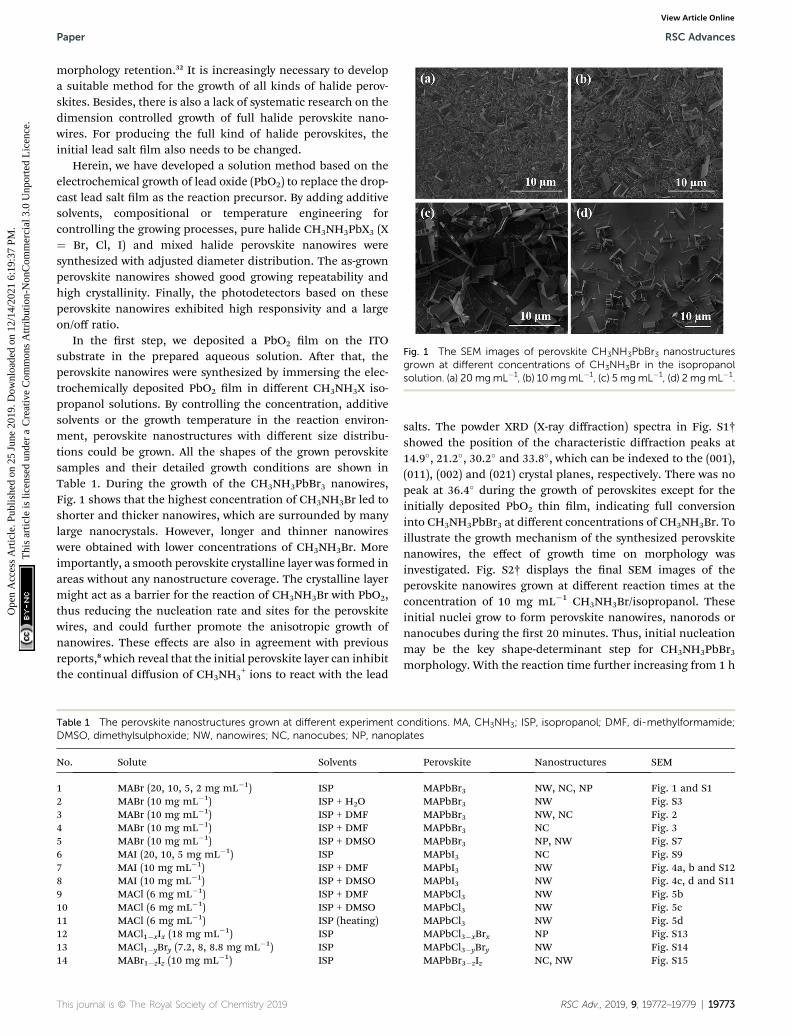
Fig. 1 The SEM images of perovskite CH3NH3PbBr3 nanostructuresgrown at different concentrations of CH3NH3Br in the isopropanolsolution. (a) 20mgmL�1, (b) 10mgmL�1, (c) 5 mgmL�1, (d) 2 mgmL�1.
Paper RSC Advances
Ope
n A
cces
s A
rtic
le. P
ublis
hed
on 2
5 Ju
ne 2
019.
Dow
nloa
ded
on 1
2/14
/202
1 6:
19:3
7 PM
. T
his
artic
le is
lice
nsed
und
er a
Cre
ativ
e C
omm
ons
Attr
ibut
ion-
Non
Com
mer
cial
3.0
Unp
orte
d L
icen
ce.
View Article Online
morphology retention.32 It is increasingly necessary to developa suitable method for the growth of all kinds of halide perov-skites. Besides, there is also a lack of systematic research on thedimension controlled growth of full halide perovskite nano-wires. For producing the full kind of halide perovskites, theinitial lead salt lm also needs to be changed.
Herein, we have developed a solution method based on theelectrochemical growth of lead oxide (PbO2) to replace the drop-cast lead salt lm as the reaction precursor. By adding additivesolvents, compositional or temperature engineering forcontrolling the growing processes, pure halide CH3NH3PbX3 (X¼ Br, Cl, I) and mixed halide perovskite nanowires weresynthesized with adjusted diameter distribution. The as-grownperovskite nanowires showed good growing repeatability andhigh crystallinity. Finally, the photodetectors based on theseperovskite nanowires exhibited high responsivity and a largeon/off ratio.
In the rst step, we deposited a PbO2 lm on the ITOsubstrate in the prepared aqueous solution. Aer that, theperovskite nanowires were synthesized by immersing the elec-trochemically deposited PbO2 lm in different CH3NH3X iso-propanol solutions. By controlling the concentration, additivesolvents or the growth temperature in the reaction environ-ment, perovskite nanostructures with different size distribu-tions could be grown. All the shapes of the grown perovskitesamples and their detailed growth conditions are shown inTable 1. During the growth of the CH3NH3PbBr3 nanowires,Fig. 1 shows that the highest concentration of CH3NH3Br led toshorter and thicker nanowires, which are surrounded by manylarge nanocrystals. However, longer and thinner nanowireswere obtained with lower concentrations of CH3NH3Br. Moreimportantly, a smooth perovskite crystalline layer was formed inareas without any nanostructure coverage. The crystalline layermight act as a barrier for the reaction of CH3NH3Br with PbO2,thus reducing the nucleation rate and sites for the perovskitewires, and could further promote the anisotropic growth ofnanowires. These effects are also in agreement with previousreports,8which reveal that the initial perovskite layer can inhibitthe continual diffusion of CH3NH3
+ ions to react with the lead
Table 1 The perovskite nanostructures grown at different experiment cDMSO, dimethylsulphoxide; NW, nanowires; NC, nanocubes; NP, nanop
No. Solute Solvents
1 MABr (20, 10, 5, 2 mg mL�1) ISP2 MABr (10 mg mL�1) ISP + H2O3 MABr (10 mg mL�1) ISP + DMF4 MABr (10 mg mL�1) ISP + DMF5 MABr (10 mg mL�1) ISP + DMSO6 MAI (20, 10, 5 mg mL�1) ISP7 MAI (10 mg mL�1) ISP + DMF8 MAI (10 mg mL�1) ISP + DMSO9 MACl (6 mg mL�1) ISP + DMF10 MACl (6 mg mL�1) ISP + DMSO11 MACl (6 mg mL�1) ISP (heating)12 MACl1�xIx (18 mg mL�1) ISP13 MACl1�yBry (7.2, 8, 8.8 mg mL�1) ISP14 MABr1�zIz (10 mg mL�1) ISP
This journal is © The Royal Society of Chemistry 2019
salts. The powder XRD (X-ray diffraction) spectra in Fig. S1†showed the position of the characteristic diffraction peaks at14.9�, 21.2�, 30.2� and 33.8�, which can be indexed to the (001),(011), (002) and (021) crystal planes, respectively. There was nopeak at 36.4� during the growth of perovskites except for theinitially deposited PbO2 thin lm, indicating full conversioninto CH3NH3PbBr3 at different concentrations of CH3NH3Br. Toillustrate the growth mechanism of the synthesized perovskitenanowires, the effect of growth time on morphology wasinvestigated. Fig. S2† displays the nal SEM images of theperovskite nanowires grown at different reaction times at theconcentration of 10 mg mL�1 CH3NH3Br/isopropanol. Theseinitial nuclei grow to form perovskite nanowires, nanorods ornanocubes during the rst 20 minutes. Thus, initial nucleationmay be the key shape-determinant step for CH3NH3PbBr3morphology. With the reaction time further increasing from 1 h
onditions. MA, CH3NH3; ISP, isopropanol; DMF, di-methylformamide;lates
Perovskite Nanostructures SEM
MAPbBr3 NW, NC, NP Fig. 1 and S1MAPbBr3 NW Fig. S3MAPbBr3 NW, NC Fig. 2MAPbBr3 NC Fig. 3MAPbBr3 NP, NW Fig. S7MAPbI3 NC Fig. S9MAPbI3 NW Fig. 4a, b and S12MAPbI3 NW Fig. 4c, d and S11MAPbCl3 NW Fig. 5bMAPbCl3 NW Fig. 5cMAPbCl3 NW Fig. 5dMAPbCl3�xBrx NP Fig. S13MAPbCl3�yBry NW Fig. S14MAPbBr3�zIz NC, NW Fig. S15
RSC Adv., 2019, 9, 19772–19779 | 19773

Fig. 2 The SEM images of the perovskite CH3NH3PbBr3 nanowiresgrownwith different added volumes of DMF in 1 mL isopropanol. (a) 10mL, (b) 20 mL, (c) 50 mL, (d) 80 mL, (e) 100 mL, (f) the magnified image ofa selected area in (e). (g) The corresponding length distributions and (h)PXRD patterns.
RSC Advances Paper
Ope
n A
cces
s A
rtic
le. P
ublis
hed
on 2
5 Ju
ne 2
019.
Dow
nloa
ded
on 1
2/14
/202
1 6:
19:3
7 PM
. T
his
artic
le is
lice
nsed
und
er a
Cre
ativ
e C
omm
ons
Attr
ibut
ion-
Non
Com
mer
cial
3.0
Unp
orte
d L
icen
ce.
View Article Online
to 4 h, the diameters increased slowly due to the dissolution–recrystallization processes. Consequently, the nanowiresdominated the CH3NH3PbBr3 sample with high crystallineorder. Considering the above experimental results and previousstudies,34–36 the potential growth processes can be written asfollows:
CH3NH3Br 4 CH3NH2 + HBr (1)
PbO2 + 4HBr / PbBr2 + 2H2O + Br2 (2)
PbBr2 + CH3NH3Br / CH3NH3PbBr3 (3)
PbO2 + 5CH3NH3Br / CH3NH3PbBr3 + 4CH3NH2 + 2H2O +
Br2 (4)
Briey, CH3NH3Br rstly decomposes to methylamine(CH3NH2) and hydrogen bromide (HBr) in the isopropanolsolvent with a reversible equilibrium (eqn (1)). The released HBrreacts quickly with PbO2 to form lead bromide (PbBr2) ondipping the PbO2 lm into the above-mentioned CH3NH3Brsolution (eqn (2)). Thus, it facilitates the shi of eqn (1) towardsthe positive direction to keep the reaction balance, leading toa positive decomposition of CH3NH3Br for providing HBr toreduce Pb4+ to Pb2+. As the reaction goes on, PbBr2, in turn,reacts quickly with the excess CH3NH3Br solute and eventuallygrows into CH3NH3PbBr3 due to the low activation energyrequired in this conversion process (eqn (3)). Consistent withour experimental results, no typical diffraction peaks of PbBr2could be detected in the PXRD patterns (Fig. S1†). The totalreaction equations are summed up in eqn (4), which shows thatwater molecules (H2O) are the byproducts of the nal perovskiteformation. To elucidate the role of H2O in the perovskite growthprocess, additional water molecules were added in the CH3-NH3Br isopropanol solution. Fig. S3† shows that the nanocubesoccupied a large ratio of the nanostructures at a low concen-tration of H2O and the nanowires grew only at the intervals ofthe nanocubes. At a high concentration of H2O, all the nano-structure growth processes were inhibited, resulting in theformation of a CH3NH3PbBr3 lm. The PXRD patterns inFig. S4† show two new peaks of PbBr2 appearing at 17.7� and35.9� when the H2O content reached up to 80 mL, indicating thedecomposition of the perovskite CH3NH3PbBr3.37 However, anappropriate amount of H2O is also benecial to the crystalgrowth of perovskite, as previous articles have reported.38 Theseresults indicated that, if we could control the reaction processesin eqn (4), the growth of perovskite nanostructures could bemanipulated. Fortunately, we found methods to change thereaction environment by adding an additional solvent to theprecursor solution.
Fig. 2a–f show the SEM images of the CH3NH3PbBr3 nano-wires grown with different added volumes of DMF in 1 mLisopropanol solution of CH3NH3Br (10 mg mL�1). The growthtime was set at 4 h to ensure a complete reaction of PbO2 withCH3NH3Br. Fig. 2g shows that the average length of the nano-wire increased from a few microns to 20 microns as the DMF
19774 | RSC Adv., 2019, 9, 19772–19779
concentration increased. Fig. 2h shows that all the diffractionpeaks could be well indexed to the as-synthesized perovskiteCH3NH3PbBr3, indicating good crystallization. The morphologyof the CH3NH3PbBr3 nanowires varied greatly with the changein DMF concentration, which illustrates that DMF is a crucialfactor for the nal morphology of the perovskite nano-structures. As the DMF concentration increased, the nanowiresexhibited a larger dimension, lower density and broader sizedistribution. The nanowires even presented two stable size ratiodistributions (length� 3 mmwith width� 100 nm and length�20 mmwith width� 800 nm) when the DMF volume increased to50 mL. This phenomenon has been rarely reported so far.Synthesizing perovskite nanowires of sizes smaller than 100 nmvia this method is more difficult than that via the colloidalsynthetic methods.39,40 These results could be attributed to thedissolution–recrystallization processes facilitated by DMF,which controls the nucleation and seed growth stages, based onthe kinetic theory.28 Due to the high solubility of perovskite inDMF, the initial nucleation of the perovskite was inhibited, thusmoderating the perovskite crystal growth processes. However,when the perovskite in the mixed solutions reached supersat-uration, DMF could not only provide the source materials fornanowire growth but also induce the formation of new nucle-ation sites. Thus, a broader size distribution of the nanowireswas obtained. In addition, the formation of nanowires smallerthan 100 nm in size was due to the new nucleation sites, whichare discussed in detail below. The new nucleation sites couldhave hindered nanowire growth by consuming all the newlyformed perovskites, thus leading to the formation of theperovskite lm (Fig. S5†).
This journal is © The Royal Society of Chemistry 2019

Paper RSC Advances
Ope
n A
cces
s A
rtic
le. P
ublis
hed
on 2
5 Ju
ne 2
019.
Dow
nloa
ded
on 1
2/14
/202
1 6:
19:3
7 PM
. T
his
artic
le is
lice
nsed
und
er a
Cre
ativ
e C
omm
ons
Attr
ibut
ion-
Non
Com
mer
cial
3.0
Unp
orte
d L
icen
ce.
View Article Online
In order to conrm the above-mentioned hypothesis thatDMF affects the nal morphology of the CH3NH3PbBr3 nano-wires, the nanowires grown at different reaction times wereinvestigated. During the initial formation of CH3NH3PbBr3, theinitial nucleation sites were scattered on the surface of the PbO2
lm (Fig. 3a). The number of nucleation sites was signicantlyreduced compared with that without DMF (Fig. S2†), whichconrms our assumption that the DMF can inhibit the initialnucleation of the perovskite nanostructures. When the growthtime increased from 1 min to 30 min, the nanocubes tended togrow quickly with a lower density at the expense of sacricingthe small grains; some nanowires also started to grow from thenanocubes (Fig. 3a–c). As the reaction time further increased to60 min, the nanowires grew longer and thicker with a highdensity (Fig. 3d). Very thin nanowires had also begun to form insome areas (Fig. S6†). These results are well consistent with ourabove explanation that DMF can induce new nucleation siteswhen the perovskite reaches supersaturation in mixed solu-tions, thus leading to the formation of thinner nanowires aerreacting for several tens of minutes. The corresponding diam-eter distributions were counted, as shown in Fig. 3e and f. Allthe diameter distributions presented good Gaussian curves,where the mean diameter increased from 450 nm to 900 nmalong with the increase in the reaction time. Besides, to illus-trate that the role of DMF is not unique, we also investigated theeffect of DMSO on the growth of the perovskite CH3NH3PbBr3.As the DMSO concentration increased, the morphology ofCH3NH3PbBr3 transformed from nanowires to nanoplates(Fig. S7†), and the PXRD patterns also conrmed the change asthe diffraction peak at 21.2� disappeared apparently (Fig. S8†).The direction of thickness growth was consistent with thedominant (001) series of crystal planes in the XRD patterns.41
The CH3NH3PbBr3 lm was also formed when the content of
Fig. 3 The nanostructures of perovskite CH3NH3PbBr3 grown at variouprecursor CH3NH3Br/ISP solution was at a stable concentration of 10 mbutions during the initial nucleation and crystal growth of the perovskite athe Gaussian fitting curves of the statistical histograms.
This journal is © The Royal Society of Chemistry 2019
DMSO increased to 200 mL, although a new peak belonging toPbBr2 emerged at 35.2�. On further controlling the crystalliza-tion process of the perovskite by adjusting the amount of theextra additive DMSO, high-quality single crystal perovskiteCH3NH3PbBr3 lms could be obtained.
To illustrate the universality of our approach, we extended itto synthesize various compositional perovskite nanowires justby replacing CH3NH3Br with other halide precursors as thestarting solute. Although in the initial step, the perovskiteCH3NH3PbI3 could be only grown into cube-like nanostructuresat different concentrations of CH3NH3I (Fig. S9†), ultralong(hundred microns) white-phase CH3NH3PbI3 nanowires couldbe formed when DMF was added in the MAI/ISP solution(Fig. 4a). This is consistent with previous studies,42,43 whichreport that CH3NH3I–PbI2–DMF intermediate phases can beformed in the mixed solution despite different initial lead saltlms. Aer annealing at 100 �C for 15 min, the color of theperovskite gradually changed from white to black. Fig. 4b showsthe morphology of the grown perovskite without any changesaer annealing, illustrating that pure perovskite CH3NH3PbI3nanowires can be formed from CH3NH3I–PbI2–DMF interme-diate phases. Besides, Fig. 4c and d show that DMSO has thesame effect as DMF; that is, the nanowires could be transformedfrom the intermediate phase of CH3NH3I–PbI2–DMSO aerannealing. The PXRD patterns in Fig. S10† conrmed theintermediate phases of CH3NH3I–PbI2–DMF and CH3NH3I–PbI2–DMSO formed aer the corresponding solvents wereadded.
The presence of CH3NH3PbI3 characteristic peaks (red lines)illustrated the synthesis of perovskite CH3NH3PbI3 aerannealing. Although a little peak of PbI2 emerged at 12.7�,8 thepure perovskite CH3NH3PbI3 nanowires could be formed byoptimizing the growth parameters. Fig. S11 and S12† show that
s reaction times: (a) 1 min, (b) 10 min, (c) 30 min and (d) 60 min. Theg mL�1 with 100 mL DMF additive. The corresponding diameter distri-re shown in (e)–(h), respectively. The various colored (dashed) lines are
RSC Adv., 2019, 9, 19772–19779 | 19775

Fig. 4 The SEM images of perovskite CH3NH3PbI3 nanowires (a)grown with 30 mL DMF added into 1 mL isopropanol solution and (b)the corresponding samples after annealing at 100 �C for 15 minutes.The perovskite CH3NH3PbI3 nanowires (c) grown with 10 mL DMSOadded into the isopropanol solution and (d) the correspondingsamples after annealing at 100 �C for 15 minutes. The concentration ofMAI/ISP solution was 10 mg mL�1.
Fig. 5 The SEM images of the perovskite CH3NH3PbCl3 nano-structures grown at different reactive environments. (a) Roomtemperature without DMF in isopropanol solution, (b) 50 mL DMF in1 mL isopropanol solution, (c) 50 mL DMSO in 1 mL isopropanolsolution, and (d) 80 �C. The concentration of MACl/ISP solution was6 mg mL�1.
Fig. 6 (a) The PXRD patterns of the multiple compositional perovskitenanostructures grown at different halide ratios in the precursor solu-tion. (b) Widely tunable fluorescence emission wavelength from theas-grown mixed halide perovskites.
RSC Advances Paper
Ope
n A
cces
s A
rtic
le. P
ublis
hed
on 2
5 Ju
ne 2
019.
Dow
nloa
ded
on 1
2/14
/202
1 6:
19:3
7 PM
. T
his
artic
le is
lice
nsed
und
er a
Cre
ativ
e C
omm
ons
Attr
ibut
ion-
Non
Com
mer
cial
3.0
Unp
orte
d L
icen
ce.
View Article Online
the intermediate phases of CH3NH3PbI3 could be synthesized atdifferent concentrations of DMF and DMSO, respectively.Considering that the annealing processes did not affect the nalmorphology of the perovskite products, we believed that thecorresponding pure perovskite CH3NH3PbI3 nanowires could beobtained aer annealing.
For CH3NH3PbCl3, no change in the PbO2 lm could beobserved when we immersed the PbO2 lm in CH3NH3Cl iso-propanol solution for more than ten hours (Fig. 5a). This resultillustrated that they could not react with each other due to thehigh nucleation energy required at room temperature. However,when an extra additive of 50 mL DMF or DMSO was added in theCH3NH3Cl isopropanol solution, the perovskite CH3NH3PbCl3nanowires could be grown within hours. The extra additivesolvents could act as a catalyst, which provides an intermediaryprocess for the growth of CH3NH3PbCl3. As shown in Fig. 5band c, the CH3NH3PbCl3 nanowires grew on the substrate witha large pitch distribution. Fig. 5d shows that the CH3NH3PbCl3nanowires could also grow at a high reaction temperaturewithin dozens of minutes, indicating that the nucleation barriercould be overcome effectively. The broader size distributions ofthe nanowires can be attributed to the simultaneous occurrenceof nucleation and crystal growth processes.
According to our previous research,44 mixed halides play animportant role in the growth of perovskite nanostructures. Wehave shown that the CH3NH3PbCl3�xIx nanoplates can be grownat a specic concentration ratio. When we immersed the PbO2
lm in the solution with 1 : 1 concentration ratio of CH3NH3Cland CH3NH3I, nanoplates could be generated (Fig. S13†). Themixed halide perovskite CH3NH3PbCl3�yBry and CH3NH3-PbBr3�zIz nanowires could be grown at different halide ratios of
19776 | RSC Adv., 2019, 9, 19772–19779
CH3NH3I : CH3NH3Br and CH3NH3Br : CH3NH3Cl in iso-propanol solution, respectively (Fig. S14 and S15†). The PXRDpatterns in Fig. 6a display that the major characteristicdiffraction peaks of the multiple component perovskites canshi from 15.6� to 14� as the halide changes from chloride toiodide gradually, illustrating that the mixed halide perovskitesgrew with expected crystal structures. These results are inagreement with similar reports.45–47 On increasing the x value ofCH3NH3I1�xBrx and CH3NH3Br1�xClx in the reactive iso-propanol solution, the x in the synthesized perovskite CH3-NH3PbI3�xBrx and CH3NH3PbBr3�xClx will be increased too.Thus, perovskites with different compositions can be obtained.This wide component control of perovskites led to broadwavelength tunability. As shown in Fig. 6b, the uorescenceemission spectra of the as-grown perovskites could change fromnear-infrared (779 nm) to blue (408 nm), covering the full visibleregion. The corresponding optical bandgap (Eg) could becalculated approximately, according to the equation Eg ¼ 1240/
This journal is © The Royal Society of Chemistry 2019
Paper RSC Advances
Ope
n A
cces
s A
rtic
le. P
ublis
hed
on 2
5 Ju
ne 2
019.
Dow
nloa
ded
on 1
2/14
/202
1 6:
19:3
7 PM
. T
his
artic
le is
lice
nsed
und
er a
Cre
ativ
e C
omm
ons
Attr
ibut
ion-
Non
Com
mer
cial
3.0
Unp
orte
d L
icen
ce.
View Article Online
l,48 where l is the central wavelength of the emission spectrum.From the derived peak positions of l, the Eg values were esti-mated in the range of 3.04–1.59 eV, which correlated well withprevious studies.49
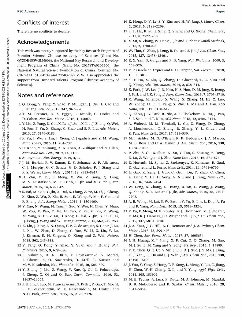
To investigate the optoelectronic properties of the perovskitenanowires synthesized by our method, photodetectors based onthe CH3NH3PbBr3 nanowires were fabricated on a gold inter-digital electrode, which was deposited on the quartz substratewith 60 nm in thickness under a designed macro mask plate.Fig. 7a shows the optical microscopy image of a real perovskitenanowire photodetector, where the nanowire is well located inthe gap between the two separate electrodes. Upon illuminatingwith a 450 nm laser, the photocurrent shows an almost linearand symmetrical variation versus the voltage at different lasingpower densities (Fig. 7b), indicating good ohmic contactbetween the perovskite and the gold electrode. Ohmic contactimplies that the junction barrier between the gold electrode andperovskite is small, indicating that the hot electrons may alsocontribute to the high responsivity in photodetection.50 Underthe applied voltage of 2 V, the photocurrent could reach 48 nAwith light illumination at a power density of 83.3 mW cm�2. Thedark current was as small as 0.01 nA, which could be extractedfrom the black line shown in Fig. 7b. Thus, the on/off ratio wascalculated to be �5 � 103, which is larger than those of theperovskite photodetectors reported recently.51,52 Fig. 7c plots thephotocurrent and photoresponsivity against the light powerunder the same voltage of 2 V. The photocurrent shows a nearlylinear upward trend with increasing light power, suggestingthat the photoinduced carriers are proportional to the incidentphotons, which indicates fewer traps or defects in the obtainedperovskite nanowires. The corresponding photoresponsivity Rcan be extracted from the equation R ¼ Iph/PS, where Iph is thephotocurrent, P is the incident light power, and S is the effective
Fig. 7 Optoelectronic property characterization of the perovskiteCH3NH3PbBr3 nanowire photodetectors with 450 nm light irradiation.(a) Optical image of a perovskite nanowire photodetector. (b) Darkcurrent and photocurrents of the perovskite nanowire photodetectorsat various power densities. (c) Photocurrent and photoresponsivitymeasured at different illumination powers with a voltage of 2 V. (d)Time-dependent photocurrent curves of the perovskite nanowirephotodetectors at a voltage of 10 V.
This journal is © The Royal Society of Chemistry 2019
absorbing area of the photodetectors. Accordingly, the calcu-lated R shows a decreasing trend from 2.1 to 0.6 AW�1 when theincident power increased from 2 to 25mW. This may be becausethe carrier recombination was enhanced at high illuminationpower. As observed in the measurement process, the greenuorescence of the nanowire was very obvious under highirradiation. Even so, the photoresponsivity of the photodetec-tors could reach up to 2.1 A W�1, which is superior to those ofthe previously reported perovskite detectors.51–54 Besides the on/off ratio and responsivity characterization of the photodetector,the specic detectivity (D*) also acts as an important parameterthat reects the ability to detect weak light signals. Assumingthat shot noise dominates the dark current, D* can be estimatedfrom the expression D* ¼ RS1/2/(2qId)
1/2, where q is the unitcharge and Id is the dark current.55 Thus, the maximum specicdetectivity was then estimated to be 1.2 � 1012 jones (jones¼ cm Hz1/2 W�1). For revealing the time response characteris-tics of the perovskite photodetectors, time-dependent photo-current was measured, as shown in Fig. 7d. As soon as thephotodetector was illuminated, the current rose drastically witha narrow peak due to the sudden excitation of carriers, whichdeparted quickly and caused the photocurrent to stabilize.56 Onblocking the light source, the current declined drastically.Similar current values cycled several times without muchchange under the light on and off conditions, displaying thegood switching and repeatable performances of the photode-tector. A high-resolution single cycle time response curve isshown in Fig. S16,† displaying a rise time of less than 0.9 s anda decay time of less than 0.2 s for the perovskite photodetector.Moreover, Fig. S17† also shows that the perovskite CH3NH3PbI3nanowire photodetector is photoresponsive to the 450 nm laser,although the detection performance is inferior to that of theperovskite CH3NH3PbBr3 photodetector. This may be due to therough surface and poor crystal quality of the perovskite CH3-NH3PbI3 nanowires that were transformed from the interme-diate phase.
Conclusions
In summary, we demonstrate that tunable bandgap perovskitenanowires can be synthesized by reacting the electrochemicallydeposited PbO2 lm with the CH3NH3X (X ¼ Br, I, Cl) or mixedhalide solutes in isopropanol solution. By controlling thenucleation and growth processes with multiple engineeringtechniques, the structures and diameter distributions of theperovskite nanowires can be manipulated effectively. Althoughthe nanowires grown by this method are cluttered on thesubstrate, we think this problem can be solved by the graphicdeposition of lead oxide in the future. Looking forward, thissimple electrochemically assisted controllable solution methodcould provide a new route for producing high-quality nano-materials, especially perovskite nanomaterials, which arepromising materials for applications in optoelectronic devices.For instance, the photodetectors we fabricated based on theCH3NH3PbBr3 nanowires exhibit a high responsivity of 2.1 AW�1 and an on/off ratio of 5 � 103.
RSC Adv., 2019, 9, 19772–19779 | 19777
RSC Advances Paper
Ope
n A
cces
s A
rtic
le. P
ublis
hed
on 2
5 Ju
ne 2
019.
Dow
nloa
ded
on 1
2/14
/202
1 6:
19:3
7 PM
. T
his
artic
le is
lice
nsed
und
er a
Cre
ativ
e C
omm
ons
Attr
ibut
ion-
Non
Com
mer
cial
3.0
Unp
orte
d L
icen
ce.
View Article Online
Conflicts of interest
There are no conicts to declare.
Acknowledgements
This work wasmostly supported by the Key Research Program ofFrontier Science, Chinese Academy of Sciences (Grant No.QYZDB-SSW-SLH006), the National Key Research and Develop-ment Program of China (Grant No. 2017YFA0206600), theNational Natural Science Foundation of China (Contract No.61674141, 61504134 and 21503209). Z. W. also appreciates thesupport from Hundred Talents Program (Chinese Academy ofSciences).
Notes and references
1 Q. Dong, Y. Fang, Y. Shao, P. Mulligan, J. Qiu, L. Cao andJ. Huang, Science, 2015, 347, 967–970.
2 T. M. Brenner, D. A. Egger, L. Kronik, G. Hodes andD. Cahen, Nat. Rev. Mater., 2016, 1, 15007.
3 Y. Liu, Z. Yang, D. Cui, X. Ren, J. Sun, X. Liu, J. Zhang, Q.Wei,H. Fan, F. Yu, X. Zhang, C. Zhao and S. F. Liu, Adv. Mater.,2015, 27, 5176–5183.
4 P. Yu, J. Wu, S. Liu, J. Xiong, C. Jagadish and Z. M. Wang,Nano Today, 2016, 11, 704–737.
5 U. Khan, Y. Zhinong, A. A. Khan, A. Zulqar and N. Ullah,Nanoscale Res. Lett., 2019, 14, 116.
6 Anonymous, Nat. Energy, 2019, 4, 1.7 J. M. Buriak, P. V. Kamat, K. S. Schanze, A. P. Alivisatos,C. J. Murphy, G. C. Schatz, G. D. Scholes, P. J. Stang andP. S. Weiss, Chem. Mater., 2017, 29, 8915–8917.
8 H. Zhu, Y. Fu, F. Meng, X. Wu, Z. Gong, Q. Ding,M. V. Gustafsson, M. T. Trinh, S. Jin and X. Y. Zhu, Nat.Mater., 2015, 14, 636–642.
9 S. Bai, M. Cao, Y. Jin, X. Dai, X. Liang, Z. Ye, M. Li, J. Cheng,X. Xiao, Z. Wu, Z. Xia, B. Sun, E. Wang, Y. Mo, F. Gao andF. Zhang, Adv. Energy Mater., 2014, 4, 1301460.
10 Y. Cao, N. Wang, H. Tian, J. Guo, Y. Wei, H. Chen, Y. Miao,W. Zou, K. Pan, Y. He, H. Cao, Y. Ke, M. Xu, Y. Wang,M. Yang, K. Du, Z. Fu, D. Kong, D. Dai, Y. Jin, G. Li, H. Li,Q. Peng, J. Wang and W. Huang, Nature, 2018, 562, 249–253.
11 K. Lin, J. Xing, L. N. Quan, F. P. G. de Arquer, X. Gong, J. Lu,L. Xie, W. Zhao, D. Zhang, C. Yan, W. Li, X. Liu, Y. Lu,J. Kirman, E. H. Sargent, Q. Xiong and Z. Wei, Nature,2018, 562, 245–248.
12 Y. Fang, Q. Dong, Y. Shao, Y. Yuan and J. Huang, Nat.Photonics, 2015, 9, 679–686.
13 S. Yakunin, D. N. Dirin, Y. Shynkarenko, V. Morad,I. Cherniukh, O. Nazarenko, D. Kreil, T. Nauser andM. V. Kovalenko, Nat. Photonics, 2016, 10, 585–589.
14 Y. Zhang, J. Liu, Z. Wang, Y. Xue, Q. Ou, L. Polavarapu,J. Zheng, X. Qi and Q. Bao, Chem. Commun., 2016, 52,13637–13655.
15 J. H. Im, J. Luo, M. Franckevicius, N. Pellet, P. Gao, T. Moehl,S. M. Zakeeruddin, M. K. Nazeeruddin, M. Gratzel andN. G. Park, Nano Lett., 2015, 15, 2120–2126.
19778 | RSC Adv., 2019, 9, 19772–19779
16 K. Hong, Q. V. Le, S. Y. Kim and H. W. Jang, J. Mater. Chem.C, 2018, 6, 2189–2209.
17 S. T. Ha, R. Su, J. Xing, Q. Zhang and Q. Xiong, Chem. Sci.,2017, 8, 2522–2536.
18 X. Xu, X. Zhang, W. Deng, J. Jie and X. Zhang, Small Methods,2018, 2, 1700340.
19 W. Tian, C. Zhao, J. Leng, R. Cui and S. Jin, J. Am. Chem. Soc.,2015, 137, 12458–12461.
20 R. X. Yan, D. Gargas and P. D. Yang, Nat. Photonics, 2009, 3,569–576.
21 F. P. Garcıa de Arquer and E. H. Sargent, Nat. Electron., 2018,1, 380–381.
22 S. T. Ha, X. Liu, Q. Zhang, D. Giovanni, T. C. Sum andQ. Xiong, Adv. Opt. Mater., 2014, 2, 838–844.
23 K. Park, J. W. Lee, J. D. Kim, N. S. Han, D. M. Jang, S. Jeong,J. Park and J. K. Song, J. Phys. Chem. Lett., 2016, 7, 3703–3710.
24 X. Wang, M. Shoaib, X. Wang, X. Zhang, M. He, Z. Luo,W. Zheng, H. Li, T. Yang, X. Zhu, L. Ma and A. Pan, ACSNano, 2018, 12, 6170–6178.
25 Q. Zhou, J. G. Park, R. Nie, A. K. Thokchom, D. Ha, J. Pan,S. I. Seok and T. Kim, ACS Nano, 2018, 12, 8406–8414.
26 A. Waleed, M. M. Tavakoli, L. Gu, Z. Wang, D. Zhang,A. Manikandan, Q. Zhang, R. Zhang, Y. L. Chueh andZ. Fan, Nano Lett., 2017, 17, 523–530.
27 M. J. Ashley, M. N. O'Brien, K. R. Hedderick, J. A. Mason,M. B. Ross and C. A. Mirkin, J. Am. Chem. Soc., 2016, 138,10096–10099.
28 P. Zhu, S. Gu, X. Shen, N. Xu, Y. Tan, S. Zhuang, Y. Deng,Z. Lu, Z. Wang and J. Zhu, Nano Lett., 2016, 16, 871–876.
29 E. Horvath, M. Spina, Z. Szekrenyes, K. Kamaras, R. Gaal,D. Gachet and L. Forro, Nano Lett., 2014, 14, 6761–6766.
30 L. Gao, K. Zeng, J. Guo, C. Ge, J. Du, Y. Zhao, C. Chen,H. Deng, Y. He, H. Song, G. Niu and J. Tang, Nano Lett.,2016, 16, 7446–7454.
31 W. Deng, X. Zhang, L. Huang, X. Xu, L. Wang, J. Wang,Q. Shang, S. T. Lee and J. Jie, Adv. Mater., 2016, 28, 2201–2208.
32 A. B. Wong, M. Lai, S. W. Eaton, Y. Yu, E. Lin, L. Dou, A. Fuand P. Yang, Nano Lett., 2015, 15, 5519–5524.
33 Y. Fu, F. Meng, M. B. Rowley, B. J. Thompson, M. J. Shearer,D. Ma, R. J. Hamers, J. C. Wright and S. Jin, J. Am. Chem. Soc.,2015, 137, 5810–5818.
34 J. A. Koza, J. C. Hill, A. C. Demster and J. A. Switzer, Chem.Mater., 2016, 28, 399–405.
35 H. Chen, Adv. Funct. Mater., 2017, 27, 1605654.36 J. H. Huang, K. J. Jiang, X. P. Cui, Q. Q. Zhang, M. Gao,
M. J. Su, L. M. Yang and Y. Song, Sci. Rep., 2015, 5, 15889.37 Y. X. Chen, Q. Q. Ge, Y. Shi, J. Liu, D. J. Xue, J. Y. Ma, J. Ding,
H. J. Yan, J. S. Hu and L. J. Wan, J. Am. Chem. Soc., 2016, 138,16196–16199.
38 J. You, Y. Yang, Z. Hong, T.-B. Song, L. Meng, Y. Liu, C. Jiang,H. Zhou, W.-H. Chang, G. Li and Y. Yang, Appl. Phys. Lett.,2014, 105, 183902.
39 M. B. Teunis, A. Jana, P. Dutta, M. A. Johnson, M. Mandal,B. B. Muhoberac and R. Sardar, Chem. Mater., 2016, 28,5043–5054.
This journal is © The Royal Society of Chemistry 2019
Paper RSC Advances
Ope
n A
cces
s A
rtic
le. P
ublis
hed
on 2
5 Ju
ne 2
019.
Dow
nloa
ded
on 1
2/14
/202
1 6:
19:3
7 PM
. T
his
artic
le is
lice
nsed
und
er a
Cre
ativ
e C
omm
ons
Attr
ibut
ion-
Non
Com
mer
cial
3.0
Unp
orte
d L
icen
ce.
View Article Online
40 C. Wang, Y. Zhang, A. Wang, Q. Wang, H. Tang, W. Shen,Z. Li and Z. Deng, Chem. Mater., 2017, 29, 2157–2166.
41 W. Zhang, L. Peng, J. Liu, A. Tang, J. S. Hu, J. Yao andY. S. Zhao, Adv. Mater., 2016, 28, 4040–4046.
42 A. A. Petrov, N. Pellet, J.-Y. Seo, N. A. Belich, D. Y. Kovalev,A. V. Shevelkov, E. A. Goodilin, S. M. Zakeeruddin,A. B. Tarasov and M. Graetzel, Chem. Mater., 2016, 29, 587–594.
43 A. A. Petrov, I. P. Sokolova, N. A. Belich, G. S. Peters,P. V. Dorovatovskii, Y. V. Zubavichus, V. N. Khrustalev,A. V. Petrov, M. Gratzel, E. A. Goodilin and A. B. Tarasov, J.Phys. Chem. C, 2017, 121, 20739–20743.
44 K. Ren, L. Huang, S. Yue, S. Lu, K. Liu, M. Azam, Z. Wang,Z. Wei, S. Qu and Z. Wang, J. Mater. Chem. C, 2017, 5,2504–2508.
45 N. K. Kumawat, A. Dey, A. Kumar, S. P. Gopinathan,K. L. Narasimhan and D. Kabra, ACS Appl. Mater.Interfaces, 2015, 7, 13119–13124.
46 A. Sadhanala, S. Ahmad, B. Zhao, N. Giesbrecht,P. M. Pearce, F. Deschler, R. L. Hoye, K. C. Godel, T. Bein,P. Docampo, S. E. Dutton, M. F. De Volder andR. H. Friend, Nano Lett., 2015, 15, 6095–6101.
47 A. Sadhanala, F. Deschler, T. H. Thomas, S. E. Dutton,K. C. Goedel, F. C. Hanusch, M. L. Lai, U. Steiner, T. Bein,
This journal is © The Royal Society of Chemistry 2019
P. Docampo, D. Cahen and R. H. Friend, J. Phys. Chem.Lett., 2014, 5, 2501–2505.
48 J. Dai, H. Zheng, C. Zhu, J. Lu and C. Xu, J. Mater. Chem. C,2016, 4, 4408–4413.
49 D. M. Jang, K. Park, D. H. Kim, J. Park, F. Shojaei, H. S. Kang,J. P. Ahn, J. W. Lee and J. K. Song, Nano Lett., 2015, 15, 5191–5199.
50 P. Yu, L. V. Besteiro, Y. Huang, J. Wu, L. Fu, H. H. Tan,C. Jagadish, G. P. Wiederrecht, A. O. Govorov and Z. Wang,Adv. Opt. Mater., 2018, 7, 1800995.
51 S. Zhuo, J. Zhang, Y. Shi, Y. Huang and B. Zhang, Angew.Chem., Int. Ed. Engl., 2015, 54, 5693–5696.
52 J. Ding, S. Du, Z. Zuo, Y. Zhao, H. Cui and X. Zhan, J. Phys.Chem. C, 2017, 121, 4917–4923.
53 F. Chen, C. Xu, Q. Xu, Y. Zhu, F. Qin, W. Zhang, Z. Zhu,W. Liu and Z. Shi, ACS Appl. Mater. Interfaces, 2018, 10,25763–25769.
54 F. Wang, J. Mei, Y. Wang, L. Zhang, H. Zhao and D. Zhao,ACS Appl. Mater. Interfaces, 2016, 8, 2840–2846.
55 D. Wang, J. Meng, X. Zhang, G. Guo, Z. Yin, H. Liu, L. Cheng,M. Gao, J. You and R. Wang, Chem. Mater., 2018, 30, 3819–3826.
56 D. Liu, Z. Hu, W. Hu, P. Wangyang, K. Yu, M. Wen, Z. Zu,J. Liu, M. Wang, W. Chen, M. Zhou, X. Tang and Z. Zang,Mater. Lett., 2017, 186, 243–246.
RSC Adv., 2019, 9, 19772–19779 | 19779