
Multilayer Thin Films for SRF Accelerating Cavities A Dissertation ...
111
Multilayer Thin Films for SRF Accelerating Cavities A Dissertation presented to the faculty of the School of Engineering and Applied Science University of Virginia In Partial Fulfillment of the requirements for the Degree Doctor of Philosophy by Daniel Leo Bowring May, 2011
Transcript of Multilayer Thin Films for SRF Accelerating Cavities A Dissertation ...

Multilayer Thin Films for SRF Accelerating Cavities
A Dissertation
presented to
the faculty of the School of Engineering and Applied Science
University of Virginia
In Partial Fulfillment
of the requirements for the Degree Doctor of Philosophy
by
Daniel Leo Bowring
May, 2011

APPROVAL SHEET
The dissertation is submitted in partial fulfillment of the
requriements for the degree of
Doctor of Philosophy
Daniel Bowring (Author)
This dissertation has been read and approved by the examining Committee:
(Dissertation advisor)
Accepted for the School of Engineering and Applied Science:
Dean, School of Engineering and Applied Science
May, 2011

Abstract
Multilayer films on the interior of a superconducting radio frequency (SRF) accelerating
cavity have the potential to increase the lower critical magnetic field Hc1 of the bulk cavity
material [A. Gurevich, Appl. Phys. Lett. 88, 012511 (2006)]. A cavity with enhanced
Hc1 can tolerate higher accelerating gradients, allowing for the construction of SRF par-
ticle accelerators with lower capital costs, and more stable beams and cryogenic systems.
Multilayer films are composed of alternating layers of insulator and superconductor, each
of which layer is thinner than the London penetration depth of the superconductor. This
dissertation presents an experimental program for the evaluation of multilayer thin films
for SRF, as well as the first evaluation of such films in the RF regime. A stripline disk res-
onator operating at 2.8 GHz supplies field to a small, flat multilayer sample, in which the
superconducting film is (Nb,Ti)N and the insulating film is Al2O3. By measuring the Q of
the resonator, Hc1 may be measured and compared with equivalent bulk superconducting
samples.
Acknowledgements
The work I performed during the course of my dissertation was extremely interdisciplinary.
Looking back, it seems like I took on a new project (and a new learning curve) every
week. I’ve been very fortunate to work with people who were willing to help me and,
more importantly, to teach me. I’d like to acknowledge their contributions here.
First, this work would not have been possible without the guidance and support of
my advisor, Blaine Norum. In particular, I’d like to thank him for getting me involved
with accelerator physics, a field I’ve found to be extremely rewarding.
I’ve been very lucky to work with Larry Phillips for the past five years. He’s been
a great teacher and a good friend. Larry, call me when you finally start selling those
vegetarian hamburgers.
I could not have made any films without the assistance and advice of Anne-Marie
Valente-Feliciano and Josh Spradlin. Thank you both very much.
During the experimental design phase, I had good advice from and interesting dis-
cussions with - alphabetically - Lance Cooley, Jean Delayen, Tom Goodman, and Charlie
Reece. Their contributions helped to make my experimental design smoother and more
efficient.
Three technicians were especially helpful to me, and regularly went out of their way
for the sake of my education. Scott Williams helped me to braize my UHV heater, as
well as giving me advice with other hardware issues. Teena Harris acid-etched UHV parts
for me so quickly, I could barely keep up with her. And Tom Elliot taught me ion beam
etching and DC magnetron sputtering.
Tom passed away recently. He was a never-ending source of jokes and stories, and
kept me laughing when things in the lab got difficult. He will be missed.

iii
Thanks very much to Xin Zhao, Kang Seo, and Olga Trofimova, who helped me
with materials characterization work. And although it wasn’t ultimately mentioned in
this dissertation, I did a fair amount of work in mechanically and chemically polishing
niobium substrates. Liang Zhao and Hui Tian helped me with some electropolishing work.
Thank you both.
One of the most important lessons I learned in grad school was that research is simply
not possible without strong administrative support. Very warm thanks to Carolyn Camp,
Crystal Baker, Vickie Thomas, Susan Hull, Tammie Shifflet, Dawn Shifflet, and Suzie
Garrett for their hard work and attention to detail.
Thanks to Jerry Floro and Bobby Weikle, who made insightful and helpful suggestions
regarding my analysis. Thanks also to my editors: Paul Mattione, Larry and Esther
Bowring, and Anaıs Miodek.
My family is the foundation for this work, and for all my work. To my parents, my
sister, and my extended family, thank you. I promise I won’t bring my computer to
Thanksgiving this year.
Finally, to Anaıs Miodek: thank you. Thank you. This is as much yours as it is mine.
Let’s get those pictures hung up.

For my grandparents, Sol and Anna Rolnitzky.

Contents
1 Introduction 1
1.1 Accelerator background . . . . . . . . . . . . . . . . . . . . . . . . . . . . 1
1.1.1 The transition from DC to AC accelerators . . . . . . . . . . . . . 1
1.1.2 Drift tube accelerators . . . . . . . . . . . . . . . . . . . . . . . . . 4
1.1.3 The choice of RF frequencies . . . . . . . . . . . . . . . . . . . . . 6
1.2 Cavity basics . . . . . . . . . . . . . . . . . . . . . . . . . . . . . . . . . . 7
1.2.1 Pillbox cavities . . . . . . . . . . . . . . . . . . . . . . . . . . . . . 7
1.3 Superconducting Cavities . . . . . . . . . . . . . . . . . . . . . . . . . . . 12
1.3.1 Room temperature vs. superconducting accelerators . . . . . . . . 14
1.4 Superconductivity basics . . . . . . . . . . . . . . . . . . . . . . . . . . . . 15
1.5 SRF cavities . . . . . . . . . . . . . . . . . . . . . . . . . . . . . . . . . . . 18
1.5.1 Niobium for SRF cavities . . . . . . . . . . . . . . . . . . . . . . . 18
1.5.2 Q vs. E curves . . . . . . . . . . . . . . . . . . . . . . . . . . . . . 19
1.6 Limitations of bulk Nb . . . . . . . . . . . . . . . . . . . . . . . . . . . . . 19
2 A Multilayer Film Approach to SRF Cavities 21
2.1 A. Gurevich, Applied Physics Letters 88, (2006). . . . . . . . . . . . . . . 21
2.2 Thermal effects . . . . . . . . . . . . . . . . . . . . . . . . . . . . . . . . . 24
2.3 Limits of multilayer performance . . . . . . . . . . . . . . . . . . . . . . . 26
2.4 Prior work on multilayer films . . . . . . . . . . . . . . . . . . . . . . . . . 30
3 Experimental design 32
3.1 Small samples . . . . . . . . . . . . . . . . . . . . . . . . . . . . . . . . . . 32
3.2 Experimental requirements . . . . . . . . . . . . . . . . . . . . . . . . . . 34

CONTENTS vi
3.3 Disk resonators . . . . . . . . . . . . . . . . . . . . . . . . . . . . . . . . . 35
3.4 Finite difference electromagnetic field simulations . . . . . . . . . . . . . . 37
3.5 Complete experimental design . . . . . . . . . . . . . . . . . . . . . . . . . 39
3.6 Apparatus . . . . . . . . . . . . . . . . . . . . . . . . . . . . . . . . . . . . 44
3.6.1 The Vertical Test Area and its RF control systems . . . . . . . . . 45
3.6.2 The dewar insert . . . . . . . . . . . . . . . . . . . . . . . . . . . . 46
4 Thin films 56
4.1 Niobium-titanium nitride . . . . . . . . . . . . . . . . . . . . . . . . . . . 56
4.2 The UHV system . . . . . . . . . . . . . . . . . . . . . . . . . . . . . . . . 60
4.2.1 The deposition chamber . . . . . . . . . . . . . . . . . . . . . . . . 61
4.2.2 The sample holder . . . . . . . . . . . . . . . . . . . . . . . . . . . 62
4.2.3 Magnetron sputtering . . . . . . . . . . . . . . . . . . . . . . . . . 67
4.3 Film analysis . . . . . . . . . . . . . . . . . . . . . . . . . . . . . . . . . . 69
4.3.1 Tc measurements . . . . . . . . . . . . . . . . . . . . . . . . . . . . 69
4.4 Surface analysis . . . . . . . . . . . . . . . . . . . . . . . . . . . . . . . . . 71
4.4.1 Thickness measurements . . . . . . . . . . . . . . . . . . . . . . . . 72
4.4.2 AFM . . . . . . . . . . . . . . . . . . . . . . . . . . . . . . . . . . . 72
4.4.3 Further analysis . . . . . . . . . . . . . . . . . . . . . . . . . . . . 74
5 Preliminary RF measurements and conclusions 82
5.1 RF measurement apparatus . . . . . . . . . . . . . . . . . . . . . . . . . . 82
5.2 Measurements and analysis . . . . . . . . . . . . . . . . . . . . . . . . . . 84
5.3 Conclusions . . . . . . . . . . . . . . . . . . . . . . . . . . . . . . . . . . . 85
5.4 Future work . . . . . . . . . . . . . . . . . . . . . . . . . . . . . . . . . . . 85
A Field solutions in a pillbox cavity 88

CONTENTS vii
List of symbols
A Vector potentialAi Surface area, thermal shielding layer ia Disk radiusa0 Lattice parameteraeff Effective disk radiusB Magnetic inductionc Speed of lightC,D Simulation mesh topology matricesD Electric displacementd Film thicknessE Electric fieldE0 Electric field amplitudeEacc Accelerating electric fieldEF Fermi energyEz Longitudinal electric field componente Electron chargeei Emissivity of thermal shielding layer iFe, F12 Emissivity factorsFWHM Full width at half maximumf Frequencyfnmp Frequency of mode (n,m, p)G Geometry factorG Gibbs free energyH Magnetic field (magnitude)Hc1 Lower critical magnetic field, superconductorHbulk
c1 Hc1 specific to bulk materialsHc2 Upper critical magnetic fieldHpk Cavity peak magnetic fieldHsh Superheating critical magnetic field, superconductorHv Critical field for vortex penetration, multilayer filmHφ Axial magnetic fieldh Kapitza thermal conductance~ Reduced Planck’s constantJ Electric current densityJn Bessel function of the first kindK Shape factor, Scherrer equationk Thermal conductivitykB Boltzmann’s constantk, q Wavenumberkc Cutoff wavenumberL Total thickness of superconducting layers, multilayer film

CONTENTS viii
ℓ Mean free pathℓd Drift tube lengthℓp Pillbox cavity lengthM Scattering matrix elementm Ion massN Total layers of thermal shieldingn Charge carrier densityn Unit normal vectorP Dissipated powerPc Power dissipated in a conductorPd Power dissipated in a dielectricPr Radiated powerPV Simulated volume losses, disk resonatorP (N2) Nitrogen partial pressurepi,f Quasiparticle momentaQ Quality factorQ0 Unloaded QQsim
0 ,Qcalc0 Simulated, calculated Q0
QL Loaded Q
Q Heat transfer rateq Particle charge, cyclotron equationRRR Residual resistivity ratioR0 Residual surface resistanceRlayers RF surface resistance, multilayer film materialRbulk RF surface resistance, bulk materialRp Pillbox cavity radiusRs RF surface resistance
Rs Global RF surface resistance, multilayer filmr Radius of curvature, cyclotron equationS, s Surface of integrationSij Scattering parameterT Drift tube periodT TemperatureTbath Liquid helium bath temperatureTc Superconducting critical temperatureTm Melting temperatureTEnmp Transverse electric field modeTMnmp Transverse magnetic field modet Timetan δ Dielectric loss tangentU Electromagnetic field energyu Position in film, normal to surfaceV Volume of integrationV0 Voltage across disk resonatorv Particle speed

CONTENTS 1
x Coordinate normal to cavity surfacexmn Set of zeroes for Jn
(n,m, p) Resonant mode indices(ui, vj , wk) Simulation mesh vertex coordinatesYn Bessel function of the second kindZ Atomic number
β Speed normalized to cβ Propagation phase constantβ Crystallite widthβin, βout Cavity coupling constants∆ Superconducting gap energy∆ω Bandwidth∆t Drift tube transit timeǫ Electromagnetic permittivityǫ0 Permittivity of free spaceǫeff Effective dielectric constantǫr Dielectric constantκ Ginzburg-Landau parameterλ London penetration depthµ Electromagnetic permeabilityµ0 Permeability of free spaceη Wave impedance of free spaceη Vortex drag coefficientω Angular frequencyφ0 Magnetic flux quantumρ Charge density(ρ, θ, z) Cylindrical coordinates: radial, azimuthal, longitudinal
(ρ, θ, z) Unit vectors, cylindrical coordinatesσ Conductivityξ BCS coherence length, finite ℓξ0 BCS coherence length

Chapter 1
Introduction
Multilayer thin film coatings on the interior of a superconducting radio frequency (SRF)
cavity have the potential to raise the effective lower critical magnetic field Hc1 of the bulk
cavity material [1]. A cavity with enhanced Hc1 would allow for higher accelerating fields
and/or less power dissipation, enabling the construction of less expensive SRF particle ac-
celerators with more stable beam and cryogenic parameters. To date, however, multilayer
films have not been evaluated in the RF regime. This dissertation presents experimental
work to evaluate the efficacy of multilayer films for use in SRF accelerating cavities.
1.1 Accelerator background
Broadly, an accelerating cavity is a conducting structure capable of supporting electro-
magnetic fields. The shape of the cavity determines the shape of the fields. Those fields
are then used in the acceleration of charged particle beams.
SRF cavities are complex systems; their design and construction pose many physics
and engineering challenges. This chapter will motivate the need for such cavities and
provide some historical context. In particular, the reasons for using superconductivity (the
“S” in SRF) and radio frequency power (the “RF”) in cavity systems will be discussed.
1.1.1 The transition from DC to AC accelerators
Prior to the 1930s, experimenters largely used α-particles from natural radioactive sources
as probes in studies of nuclear structure [2]. Between 1930 and 1933, two separate groups
developed methods of direct current (DC) ion acceleration for nuclear physics research.

1 Accelerator background 2
Cockcroft and Walton published work on “artificial disintegration” in 1932 using a 300 kV
DC generator [3]. Their design was, fundamentally, a low-frequency voltage signal fed
through a tube rectifier to obtain DC voltages up to 600 kV.
Then, in 1933, R.J. Van de Graaff et al. published work on what is now known
as a Van de Graaff generator [4]. In their device, insulating conveyor belts deposited
accumulated charge on spherical electrodes. The voltage between electrodes was then
used to accelerate ions through a discharge tube and into various targets. In 1937, a
group at the Massachusetts Institute of Technology used a pair of 40-foot-high electrodes
to create a 5.1 MV static potential [5].
Two main considerations limit the performance of DC accelerators: size and corona
discharge. In the former case, the above-cited 5.1 MV potential was reached by con-
structing electrodes so massive they had to be moved on railroad tracks and stored in
an “airship dock” - an airplane hangar, essentially. In the latter case, electrons subject
to large accelerating voltages may ionize ambient gas molecules resulting in a current
cascade, i.e. sparking capable of damaging or destroying the experimental apparatus.
Contemporary upper voltage limits for electrostatic accelerators fall between 25 and
30 MV [6,7]. Reaching these voltages requires elaborate engineering controls. For example,
dielectric breakdown may be suppressed by filling the volume between electrodes with SF6
- a highly dielectric gas - pressurized to more than 7 atm1. From a practical standpoint, the
problems of corona discharge and vacuum physics make electrostatic generators unsuitable
for producing voltages above a few tens of MV. Electrostatic facilities are now commonly
used for materials analysis (Rutherford backscattering, mass spectroscopy, etc.) and ion
implantation for the semiconductor industry, for example [8].
The problems associated with large static potentials were circumvented by a series
of machine designs in which one large acceleration is replaced by many smaller acceler-
ations. This natually leads to AC accelerator designs. A prominent example of this is
the cyclotron, developed by E.O. Lawrence et al. in the 1930s [9]. This accelerator was
one of the first to use high frequency, time-harmonic accelerating fields. The now-classic
cyclotron arrangement consisted of two semi-circular hollow electrodes mounted in a per-
1SF6 is non-toxic and non-flammable. However, the presence of humid air or coronal discharge effectsmay result in the synthesis of S2F10 or HF, both of which are extremely toxic.

1 Accelerator background 3
H
a
b
Figure 1.1: Side view (above) and plan view (below) of a typical cyclotron configuration.The applied magnetic field H is perpendicular to the ion’s travel path (dashed line). aand b indicate points at which the ion is accelerated. While an ion travels between a andb, the voltage must change sign.
pendicular magnetic field, as in Figure 1.1. The motion of a charge q within one of the
electrodes is given by the familiar cyclotron equation
mv2
r= qvB
where B is the ambient magnetic inductance strength, v and m are the ion speed and
mass, respectively, and r is the radius of path curvature. A potential difference across
the gap between the electrodes provides the actual acceleration2. The voltage changes
sign with a frequency such that the ions are accelerated each time they arrive at the gap:
points a and b in Figure 1.1. The overall ion motion is described approximately by a
spiral, with larger radii corresponding to higher kinetic energies. This approach, in which
AC fields provide multiple accelerations to a beam, is the basis for RF accelerators and
the associated cavities described below.
2The fledgling field of accelerator physics was then still establishing its units and nomenclature:Lawrence et al. excitedly anticipated “the production of 10,000,000 volt-protons” with this first cyclotron.

1 Accelerator background 4
1.1.2 Drift tube accelerators
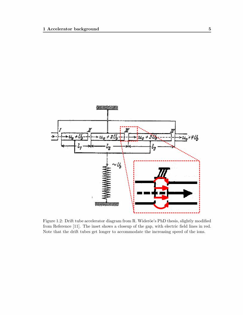
The accelerator layout most relevant to this dissertation was first conceptualized3 by
Gustav Ising in 1925 [10,11]. The design was improved upon and ultimately built by Rolf
Wideroe in 1927 for his PhD thesis, for which it accelerated Na and K ions [11]. It was
further developed by D.H. Sloan and E.O. Lawrence in the 1930s to accelerate Hg ions
[12]. In both cases, heavy ions were chosen for acceleration. Light ions and elementary
particles would ultimately accelerate to speeds approaching c - too fast for the electronic
control systems that existed at the time.
In Wideroe’s drift tube accelerator an array of collinear, hollow, conducting cylinders
served as both the beam tube and the accelerating cavities (see Figure 1.2). The beam
path was evacuated in order to maximize the mean free path of the accelerated ions. A
voltage was applied to each drift tube and that voltage oscillated, setting up longitudinal,
AC electric fields along the beamline.
In 1931, Sloan and Lawrence4 used this approach to accelerate Hg− ions to energies
around 1.26 MeV [12]. This was accomplished using a series of 30 cylinders over a total
path length of 1.14 m, with 10 MHz fields. The drift tubes were made progressively longer
to account for the ions’ acceleration. That is, the voltage phase shift between drift tubes
had to be constant, regardless of ion speed. Slight errors in the oscillator control and
the tube length were tuned away by variable inductances built into each tube’s voltage
control. Ultimately, Sloan and Lawrence concluded that the final ion energies were limited
simply by the overall number of accelerating structures and the total length of the beam
path.
Several features of the apparatus described in [12] are common to contemporary ac-
celerator facilities: discrete accelerating structures (cavities) are held at a harmonically-
3Nuclear physics was just emerging in the 1910s and 1920s, and the limitations of natural sourceswere quickly apparent. Consequently, it is difficult to clearly establish who first developed the idea of“artificial” acceleration. Credit may go to the Russians L.V. Mysovskiı and V.N. Rukavishnikov, whose1922 paper proposed a Tesla transformer to generate > 1 MV [10]. However, work was also presented in1922 by A.K. Timiryazev along similar lines, and patented (but not academically published) by J. Slepianat Westinghouse, again in 1922. It seems that in the early 1920s, “artificial acceleration” was an ideawhose time had come.
4Previous to this work, publications on drift tube accelerators were written in German or Swedish.The 1931 paper by Sloan and Lawrence is therefore discussed for convenience, being the first such workpublished in English.
1 Accelerator background 5
Figure 1.2: Drift tube accelerator diagram from R. Wideroe’s PhD thesis, slightly modifiedfrom Reference [11]. The inset shows a closeup of the gap, with electric field lines in red.Note that the drift tubes get longer to accommodate the increasing speed of the ions.

1 Accelerator background 6
varying potential and maintained at a fixed phase relative to each other; the beam path is
evacuated in order to maximize the mean free path of accelerated particles; and the final
kinetic energy of those particles is determined by each cavity’s electric field strength and
the overall length of the machine.
A good deal of work on accelerating structures was done during World War II, resulting
in variations such as traveling-wave accelerators and multi-cell cavity structures [13]5.
Machines built in the 1950s and 1960s achieved final beam energies on the order of GeV.
Contemporary machines may reach energies on the order of TeV, using cavities that
operate at frequencies ranging from a few hundred MHz to several GHz (i.e. “radio
frequencies”).
1.1.3 The choice of RF frequencies
The previous section presents the case for AC voltage sources in accelerator applications.
The drift tube accelerators discussed above, as well as most modern designs, run at radio
frequencies (RF). To see why, take the example of the drift tubes shown in Figue 1.2.
Ions in that design are accelerated at each gap between drift tubes: at points I, II, III,
etc. Consistent acceleration occurs when the drift tube voltages are always π radians out
of phase with each other - the so-called π-mode. In that mode, an ion “sees” an electric
field maximum at the gap between drift tubes and is accelerated into the tube. While
the ion is in the tube, the voltage of that tube must change polarity so that when the ion
leaves the tube, it again sees an electric field maximum.
Consider the transit time ∆t for a single particle to move from the beginning of one
drift tube to the beginning of the next, a distance ℓd. During that time, the voltage on
the tube must oscillate through half a period T . Assuming that the change in speed ∆v
is a small fraction of the total speed v = βc,
∆t = T/2
ℓd/βc = 1/2f
f = βc/2ℓ.
5Evidently, Leon Brillouin’s work on electrons in periodic potentials extends past his well-known solidstate work [14] to include electrons in periodic accelerating structures. See especially [15].

1 Cavity basics 7
This relation holds true whether the above math is done in the reference frame of the
drift tube or that of the particle.
Electrons in modern machines approach the speed of light almost instantly. In that
case, a drift length ℓd = 10 cm requires a frequency of 1.5 GHz. Lower frequencies
require longer drift tubes: 100 MHz corresponds to a one-meter-long tube, and so on.
RF frequencies are chosen to make the length of an accelerator and its component parts
manageable6.
Finally, note that the gap fields must radiate power, limiting the efficiency of the
drift tube acceleration scheme. The problem of radiative losses at the gap is overcome
by enclosing the gap between drift tubes - the region of acceleration - in a conducting
surface. This is the basis for all accelerating cavities [16].
1.2 Cavity basics
The “RF” in SRF was addressed in Sections 1.1.1 and 1.1.3. In order to address the “S”
an overview of cavity fundamentals is appropriate here. Various cavity parameters and
figures of merit will be introduced in the context of a very simple cylindrical cavity: the
“pillbox” geometry.
1.2.1 Pillbox cavities
A pillbox cavity is a hollow cylinder with closed ends, as shown in Figure 1.3. The
cylindrical symmetry makes an analytic field solution possible. For simplicity, a pillbox
cavity is discussed below with both a length ℓp and radius Rp of 10 cm.
Field solutions
The shape and frequency of the electromagnetic standing waves in a pillbox are ana-
lytically found by solving Maxwell’s equations in cylindrical coordinates with boundary
conditions set by the cavity walls. The following discussion is heavily abridged. For a
more detailed approach, see Appendix A. Assuming a linear, isotropic medium and har-
monic time-dependence eıωt with angular frequency ω for all fields, Maxwell’s equations
6Issues unique to SRF further limit the choice of frequencies for superconducting cavities. See Section1.2.

1 Cavity basics 8
(a) Pillbox cavity. (b) Electric field lines. (c) Magnetic field lines.
Figure 1.3: Pillbox cavity operating in the TM010 mode.
may be written
∇× E = − ıωµH (1.1a)
∇×H = ıωǫE + J (1.1b)
∇ ·D = ρ (1.1c)
∇ · B = 0. (1.1d)
Combining Equations 1.1a and 1.1b yields the Helmholtz wave equations
(
∇2 + ǫµω2)
[
E
B
]
= 0. (1.2)
There are then two (coupled) sets of field solutions: one for the cases in which the electric
field is longitudinal (E = Ez z) and one in which the magnetic field is longitudinal. The
former set of solutions are called transverse magnetic (TM) modes and the latter are called
transverse electric (TE) modes. There are an infinite number of modes that satisfy the
above equations. Modes are therefore labeled by indices according to their eigenvalues,
TMnmp, where n,m, and p denote field nodes along each of the basis vectors in whatever
coordinate system.
In cylindrical coordinates (ρ, θ, z),
1
ρ
∂
∂ρ
(
ρ∂Ez
∂ρ
)
+1
ρ2
∂2Ez
∂φ2+
∂2Ez
∂z2+ ω2µǫEz = 0, (1.3)
where the z-component of the electric field has been selected for simplicity. As with any
standing wave solution in cylindrical geometry, the fields take the form of Bessel functions:
Ez(ρ, φ, z) = E0Jn(kcρ) cos(nφ) sin(βz) (1.4)
1 Cavity basics 9
where k ≡√
ω2µǫ and the cutoff wavenumber kc is defined as
k2c = k2 − β2.
Application of the standard electromagnetic boundary conditions yields the dispersion
relationx2
nm
R2p
= ω2µǫ − p2π2
ℓ2p
where kcRp = xmn, the set of zeroes to the Bessel function Jn. The resonant frequency
f = ω/2π is then written
fnmp =c
2π√
µǫr
√
(xmn
R
)2
+(pπ
ℓ
)2
. (1.5)
Implicit in the above statement is the relation between c and the dielectric constant ǫr.
That is, c = 1/√
µǫ0ǫr. The cavity material here is assumed to be nonmagnetic, such that
µ = µ0.
The indices (n,m, p) give the various eigenfrequencies of the cavity fields. The fun-
damental, accelerating mode is denoted TM010 - this field has a longitudinal electric field
with no nodes, suitable for continuous acceleration through the entire length of the cavity.
Since n = p = 0 and β = 0 for this mode, Equation 1.5 simplifies to
f010 =c
2π√
ǫr
∣
∣
∣
∣
xnm
Rp
∣
∣
∣
∣
.
For ℓ = 10 cm and ǫr = 1 (i.e. vacuum), f010 = 1.1 GHz. The magnetic field corresponding
to Equation 1.4 is found directly using Maxwell’s equations, specifically Equation 1.1a.
For the TM010 mode,
H(TM010) = − ıE0
ηJ1(kρ)φ (1.6)
where η =√
µ/ǫ = 377 Ω is the wave impedance of free space.
Stored energy and power dissipation
The energy U stored in the cavity fields can be found from Equation 1.4 or 1.6. Solving for
U in terms of the magnetic fields will be useful later on, so that approach will be followed
below. Since the time-averaged field energy is distributed equally between electric and
magnetic fields,
U =1
2µ
∫
V
|H|2dV (1.7)
1 Cavity basics 10
for a volume of integration V . The integral is done by substituting Equation 1.6 and
using the identity
∫
Jν(αρ)ρdρ =ρ2
2
[
J2ν (αρ) − Jν−1(αρ)Jν+1(αρ)
]
.
Given the boundary condition J0(kR) = 0 discussed above, the second term on the right
vanishes, so
U =πℓpµR2
pE20
2η2J2
1 (kRp). (1.8)
The power P dissipated by the cavity walls is
P =1
2〈Rs〉
∫
S|H|2dS. (1.9)
Here, 〈Rs〉 is the normalized average value of the surface resistance over the whole cavity.
This discussion assumes that the surface is uniform, so 〈Rs〉 = Rs. The integral is eval-
uated on a surface S that includes the walls of the cavity at ρ = R as well as those at
z = 0, ℓ. Then
P =RsE
20
2η2
[
2πR2pJ2
1 (kRp) + ℓpRpJ21 (kRp)
]
. (1.10)
Quality factor Q
A common metric for comparing cavities - or any resonator - is the quality factor, Q. The
Q-value is, roughly speaking, a dimensionless measure of the efficiency of a cavity,
Q0 = ωU
P. (1.11)
The subscript denotes an “unloaded” Q which describes only the cavity and not the
surrounding components or the beam being accelerated. A loaded QL would account for
beam loss, inter-cavity coupling, and other, more elaborate loss mechanisms. Q0 is large
when the cavity stores large amounts of energy and the cavity walls dissipate very little
power. A commonly-cited example of a high-Q structure is a bell that rings clearly for a
long time after being struck.
Using Equations 1.8 and 1.10, the Q0 of the pillbox cavity in the TM010 mode is then
Q0 =ωµℓpRp
2Rs(Rp + ℓp). (1.12)

1 Cavity basics 11
The above expression for Q can be written as the product of two factors, one which is
a priori calculable and one, Rs, which is not. The surface resistance may be estimated
from first principles or from tables and handbooks, but an exact value depends heavily
on factors like material quality and surface preparation. Since these properties can vary
significantly from sample to sample, precise value of Rs must be measured. This leads
naturally to another figure of merit, the geometry factor G:
Q0 =G
Rs
. (1.13)
For the pillbox in question, G = ωµℓpRp/2(Rp + ℓp) = 227 Ω. (Geometry factors for
the CEBAF 1.5 GHz cavities are around 290 Ω.) In the TM010 mode, f ∝ 1/Rp which
suggests that G is entirely a measure of the aspect ratio of a cavity, and can be calculated
or simulated from first principles. Measuring Q using, for example, a vector network
analyzer will then give a precise value for Rs.
Q0 is then a way of gauging the efficiency - so to speak - of a cavity. It also determines
the fractional bandwidth:
Q0 =ω0
2∆ω. (1.14)
Equation 1.14 is derived from the generalized resonator lumped circuit model.
Resonant electron loading and non-pillbox cavity geometries
Multipacting is a resonant process by which stray electrons impact the inner walls of a
cavity and secondary electrons are emitted7. If the whole process occurs in phase with
the RF fields, a resonant positive feeback can occur: a cloud of electrons builds up in
the cavity and draws energy from the fields, sharply lowering the cavity’s Q [19]. Note
that this is a much more significant phenomenon in superconducting cavities. Since resis-
tive losses are negligible in superconducting cavities, other phenomena like multipacting
become evident. Normal-conducting cavity losses are dominated by other factors. Since
multipacting informs modern SRF cavity design and drives the departure from more ele-
mentary geometries, a brief discussion is appropriate here.
7The word itself is a modification of “multipactoring”, which seems to have been coined by PhiloT. Farnsworth, the inventor of television. He published a series of patents in the 1930s that describedamplifiers based on intentional multipactoring. [17,18].

1 Superconducting Cavities 12
The process by which “stray” electrons enter the cavity, and by which secondary
electrons are emitted, can be described to arbitrary levels of complexity. In particular,
the number of secondary electrons emitted per primary impact is a complicated function of
the kinetic energy and incident angle of the primary; the relative phase between the cavity
fields and the primary electron orbit; the electric field strength; and the surface quality of
the cavity. This latter issue is very involved, and depends heavily on the composition and
abundance of the oxides (NbO, Nb2O5) and atmospheric adsorbates (H2O, CO2, etc.) on
the inner cavity surface. These surface compounds affect the yield of secondary electrons,
but may also alter the time that secondaries require for emission, therefore changing the
phase relationship between secondaries and cavity fields [20].
In practice, multipacting is modeled with computer codes and measured in high-power
cavity tests via thermometry and spectral analysis [21, 22]. The introduction of curved
cavity geometries, first spherical and then elliptical, as well as surface treatment tech-
niques, have essentially renderend multipacting a non-issue in β = 1 cavities8 [23]. The
choice of an elliptical geometry also reduces the ratio of peak magnetic field to accelerating
electric field Hpk/Eacc (see Section 1.5) and facilitates the easy flow of chemical etchants
and rinses through a multi-cell cavity [24].
Elliptical cavity geometries are now standard for β = 1 applications. Examples in-
clude the Continuous Electron Beam Accelerator Facility (CEBAF) at Thomas Jefferson
National Accelerator Faciliy [25], the Cornell Electron Storage Ring (CESR) [26], the Spal-
lation Neutron Source (SNS) at Oak Ridge National Laboratory [27], the Large Hadron
Collider at CERN [28], the planned Internaitonal Linear Collider (ILC) [29], and many
others. A standard elliptical 5-cell, 1.5 GHz CEBAF cavity is shown in Figure 1.4a. The
electric field within a single cell is shown in Figure 1.4b and the corresponding magnetic
field is shown in Figure 1.4c.
1.3 Superconducting Cavities
This section addresses the choice of superconducting materials for RF cavities. It also
presents a brief overview of the phenomenology and theory of superconductivity.
8β = v/c = 1.

1 Superconducting Cavities 13
(a) Simulation (CST Microwave Studio) of a CEBAF 5-cell cavity. At the left-handside is the input RF power coupler. On the right-hand side is the HOM output coupler.
(b) Electric field lines (red) in CEBAF cavity. (c) Magnetic field lines (red) in CEBAF cavity.
Figure 1.4: Simulations of a standard 5-cell 1.5 GHz CEBAF Nb cavity, showing mechan-ical and field structures. The average accelerating field in such a cavity is 7.5 MV/m andthe unloaded Q ≈ 4× 10⁹. For the Poisson SuperFISH finite element simulations (b) and(c), cell boundaries are shown in blue, field lines are shown in red, and gray lines showthe finite element mesh. The simulation exploits the vertical and horizontal symmetriesof the cavity: only a quarter of the cross section is shown. The beam line runs alongthe horizontal axis. Axes show size in cm. Thanks to G. Ciovati for providing the initialinput file for this simulation.

1 Superconducting Cavities 14
1.3.1 Room temperature vs. superconducting accelerators
Whether an accelerator uses superconducting or normal conducting cavities depends on
specific physics goals, as well as environmental9, political, and budgetary constraints
[25,30,31]. Copper is typically used for room temperature machines since it is highly con-
ductive, cheap to buy, and easy to machine. However, at continuous, high RF gradients,
copper cavities dissipate a significant amount of power.
To some extent this dissipation can be ameliorated by lowering the duty cycle of the
beam, which is the ratio between the time the beam is on and the total elapsed time. A
beam with a duty cycle of unity is referred to as operating in continuous wave (CW) mode.
Normal conducting cavities with duty cycles on the order of 10−5 have reached accelerating
gradients well in excess of 100 MV/m [32]. The choice between this type of pulsed-
power acceleration and CW operation is made based on desired physics measurements
and on detector design considerations. For example, in CEBAF, electrons are scattered
off a target nucleus, perhaps liberating nucleons or mesons in the process. Establishing
which liberated nucleons coincide with which scattered electrons is termed a coincidence
measurement [33]. In pulsed-power accelerators, many electrons arrive simultaneously at
the target, making such coincidence measurements very difficult. CW machines supply a
more diffuse, continuous stream of electrons, facilitating such measurements.
Superconducting cavities were first used in the 1970s in order to achieve high-energy,
continuous beams [34]. For CW machines, liquid helium is used to cool superconducting
cavities down to a few degrees Kelvin, below their critical temperature10. Since currents
flow without resistance in a superconductor, power dissipation is much less of a concern
in SRF cavities.
Normal vs. superconducting pillbox cavity
Consider the pillbox cavity introduced in Section 1.2.1. Cavities constructed from different
materials but with identical geometries will have varying Q values depending on their
various surface resistances Rs, as in Equation 1.11. An expression for the surface resistance
9Here, “environmental” refers to seismic stability, land availability, etc.10The critical temperature Tc is the temperature below which a superconductor has zero electrical
resistivity.

1 Superconductivity basics 15
of a “good” normal conductor, i.e. one with minimal attenuation, comes straight out of
Maxwell’s equations: Rs =√
ωµ0/2σ where σ is the conductivity. Copper then, at
1.1 GHz, has a surface resistance of approximately 9 mΩ. Calculating the RF surface
resistance of a superconductor from first principles is not at all straightforward [35]. This
issue will be addressed in more detail later; for now, a rough estimate of 20 nΩ is adequate
[36].
In addition to reduced power consumption, accelerators may use SRF technology
for reasons of operational cost reduction,11 improved beam quality, and linac stability
[25,31,36,37].
1.4 Superconductivity basics
Phenomenological aspects of superconductivity are reviewed here, along with some rudi-
mentary theoretical background. Only the issues relevant to this dissertation are dis-
cussed. For a rigorous treatment, see References [38–40].
Superconductivity is a second-order phase transition (that is, a discontinuity in the
heat capacity at some critical temperature) occurring in some materials. This phase
transition is characterized by zero DC electrical resistivity below some critical temperature
Tc. Such a transition was first observed by Heike Kamerlingh Onnes in 1911, when he and
his lab staff cooled mercury down to liquid helium temperatures and measured a complete
loss of resistivity below 4.2 K.
As the resistivity vanishes, surface currents are able to instantaneously compensate for
any applied magnetic fields. Superconductors therefore exhibit perfect diamagnetism in
addition to perfect conductivity. Interior magnetic fields are expelled from the material’s
interior and external, applied fields are screened. This is known as the Meissner effect.
The London penetration depth is a consequence of the perfect diamagnetism of a
superconductor. Beneath the surface of a superconductor, fields decay like e−x/λ where
x is the coordinate normal to the surface. λ is the London penetration depth, analogous
to the skin depth of a normal conductor. Kittel [41] treats the interaction between a
plane wave vector potential A(x) = eiq·x and the ground state of a superconductor. The
11Dissipated power is related to cost reduction, but the two are not isomorphic. See Section 1.5.2.

1 Superconductivity basics 16
resulting relationship between the vector potential A and the current density j is termed
the London equation
J(x) = −ne2
mA(x)
after F. and H. London, who obtained the same result through phenomenological argu-
ments in 1935 [42]. In the above equation, n, m, and e refer to the density, mass, and
charge of charge carriers, respectively. Using Ampere’s Law (Equation 1.1b) this can be
written as
∇2H =1
λ2H
or, in one dimension,
H = H0e−x/λ. (1.15)
Implicitly, λ2 = m/ne2µ in MKS units. The London penetration depth for bulk Nb
at T = 0 K is 36 nm. In other materials, the penetration depth varies widely: thin
aluminum films may have λ ∼ 14 nm while less conventional organic superconductors
have demonstrated penetration depths on the order of mm [43,44].
In general, the transition from the superconducting state to the normal conducting
state can be mediated by an increase in temperature, magnetic field, or electrical current
above some critical value. For example, the upper RF critical field of bulk Nb is approxi-
mately 180 mT. Above this field, a cavity can be expected to “quench” - that is, be driven
into the normal state.
The first theory of superconductivity was presented in 1957 by Bardeen, Cooper, and
Schrieffer [45]. In broad terms, the so-called BCS theory demonstrates a bound state
with energy E < EF below the Fermi energy EF for electron pairs (“Cooper pairs”),
given an arbitrarily weak attractive two-body potential. For superconductors such as
Nb, this attraction between electrons comes from a combination of (a) an interaction
between lattice phonons and Cooper electrons; and (b) a screening of the typical electronic
Coulomb repulsion by the surrounding conduction electrons. The end result is a non-local
attraction between two electrons which, together, act roughly as a single charge-carrying
boson for supercurrents. The size of a Cooper pair is characterized by the coherence
length ξ0. For Nb, ξ0 = 39 nm. In imperfect crystals, for which the mean free path ℓ of

1 Superconductivity basics 17
0 0.2 0.4 0.6 0.8 1 1.20
0.2
0.4
0.6
0.8
1
1.2
∆(T
)/∆(
0)
Reduced temperature T/Tc
Figure 1.5: Approximate temperature dependence of the gap size ∆ for a generic super-conductor, as a function of reduced temperature T/Tc.
electron motion is significant, 1/ξ = 1/ξ0 + 1/ℓ. Note that in both cases, the coherence
length is much larger than any realistic interatomic spacing, such that it is possible for
many Cooper pairs to overlap each other within a superconductor.
In practice, Equation 1.15 is only valid for superconductors that operate in the local
limit. If λ ≫ ξ, then the vector potential A will vary over the characteristic size ξ of a
Cooper pair, complicating the expected value of λ.
The bound state energy E is typically within kBTc of EF. Above the Fermi surface,
there exists an energy gap 2∆ - the energy required for pair breaking. This gap is one way
to characterize the supercondcting state. The temperature dependence of ∆ is shown in
Figure 1.5 and illustrates temperature-mediated transitions from the superconducting to
the normal conducting state. Niobium is a strong candidate for SRF applications because
it has a relatively large gap: ∆(0)/kBTc = 1.9 [36].
One last phenomenon relevant to the current discussion of SRF cavities is the issue
of magnetic surface energy. As the strength of an applied magnetic field increases, the
Meissner effect breaks down and some flux may penetrate the superconductor. Materials
are classified as either Type I or Type II, depending on whether the interface between
superconducting and normal regions has positive or negative surface energy, respectively.
For Type II materials, the free energy is minimized by a maximization of the surface
area between SC and NC regions. This manifests physically as a regular distribution

1 SRF cavities 18
of flux vortices. These are quantized, much like charge, in units of the flux quantum
φ0 = 2.07 × 10⁻¹⁵ T·m2, with a size approximately equal to the coherence length ξ.
Type II superconductors are then characterized by two critical magnetic fields: a lower
critical field Hc1, above which magnetic flux vortices penetrate; and an upper critical field
Hc2 above which the material is driven into the normal conducting state. Below Hc1, the
Meissner effect is perfect and no flux penetrates.
It is possible for the superconducting state to persist metastably above Hc2, up to the
superheating critical field Hsh. There is some suggestion in the literature that this field,
and not Hc1, is the limiting field of superconducting cavities [46, 47]. The Hc1-vs-Hsh
debate is beyond the scope of this dissertation. Since surface defects and impurities can
restrict cavity operation to fields well below Hc1, the lower critical field will be treated as
the limiting field in this dissertation.
1.5 SRF cavities
SRF cavities make possible a wider variety of accelerator designs and may allow a sig-
nificant power savings in the process. However, there are certain issues unique to SRF
cavities that must then be addressed. In particular, the choice of material in cavity fab-
rication is very important. The following section motivates the use of Nb as a cavity
material, as well as the limitations of that material.
1.5.1 Niobium for SRF cavities
Bulk niobium is used in virtually all SRF machines now operating. Some low-gradient
cavity designs, such as those at SUNY Stony Brook in New York or the University of
Washington in Washington state, have used lead/tin resonators as a way to reduce capi-
tal costs [48]. However, for high-gradient, low-loss applications, Nb is the clear material of
choice [49]. Among the thousands of known superconductors, SRF cavity applications are
practically restricted to the elemental superconductors. Difficulties related to stoichiom-
etry and formability, as well as low values of Hc1, make the use of even the relatively
well-understood B1 and A15 compounds non-trivial in bulk applications12. Nb, by con-
12Recent promising efforts with bulk Nb3Sn have been presented [50]. This approach is still very muchin the R&D phase and, as a general rule, Nb is used for cavity fabrication.

1 Limitations of bulk Nb 19
Figure 1.6: Q vs. E curve for 7-cell CEBAF upgrade cavities [51].
trast, can be mined in large quantities, refined, and formed with conventional machines.
Furthermore, it is the elemental superconductor with the highest critical temperature Tc
(9.2 K) and the highest critical field Hc. It also has a relatively large energy gap ∆, as
discussed in the previous section.
1.5.2 Q vs. E curves
As discussed in Section 1.3.1, P is typically very small for superconductors, resulting
in measured Q-values on the order of 1010. As the accelerating field E increases, field-
dependent phenomena like multipacting may dissipate power in the form of heat, raising
the local temperature, driving sections of the cavity into the normal state, and precipi-
tating a quench. So-called Q vs. E curves demonstrate cavity performance limits. The
shape of such a curve may assist in the diagnosis of multipacting or field emission [36].
An example of such a curve is shown in Figure 1.6. A Q vs. H curve looks very similar,
and can be used to determine the lower critical field Hc1 of an SRF cavity. This will be
discussed in more detail in later chapters.
1.6 Limitations of bulk Nb
Although SRF cavities present some advantages to their normal conducting counterparts,
there are limits to the performance of bulk Nb. In particular, at high gradients, cavity
performance can be limited by magnetic field quenching. As previously stated, the RF
critical magnetic field for Nb is ∼180 mT. Since E and H are coupled in a cavity, this

1 Limitations of bulk Nb 20
places an upper limit on the accelerating gradient. It is not unusual for carefully prepared
single-cell cavities to approach this limit [52,53]. There is some sense, then, that bulk Nb
is slowly reaching its fundamental performance ceiling [54].
In addition to the 180 mT performance ceiling, other concerns drive research into new
SRF materials. For example, Nb has poor thermal conductivity. Local heating on the
interior surface can drive an entire cavity into the normal state [55]. Other materials
might be more efficient than Nb at transferring heat into the surrounding liquid helium
bath, and would allow for a significant improvement in cavity stability.
Finally, there are cost considerations [56]. Higher gradients would mean that fewer
cavities would be necessary for a given beam energy. This in turn implies capital cost
savings. In the same vein, material with Tc > 9.2 K would require less cooling than Nb,
saving on cryogenic costs.
There are several approaches to the problems presented above. One approach is to
construct cavities out of new materials with higher critical fields or temperatures [57,58].
Another is to coat a bulk Cu cavity with a thin superconducting film. Since fields (and
therefore currents) are contained within a penetration depth of the metal surface, only
a layer of thickness ∼ λ on the cavity interior is responsible for superconductivity itself.
The underlying Cu substrate can serve as mechanical support, thermal stabilizer, and
magnetic shielding [49, 56, 59]. This thin film approach was implemented at CERN for
the upgrade to LEP [60]. Along these lines, a multilayer thin film coating may be used to
enhance the RF critical magnetic field of a cavity [1]. This last approach will be discussed
in depth in the next chapter.

Chapter 2
A Multilayer Film Approach toSRF Cavities
The basis of this dissertation is the multilayer film approach presented by Gurevich [1], in
which the inner surface of an SRF cavity is coated with alternating thin superconducting
and insulating films. In this context, “thin” means thinner than the London penetration
depth of the superconducting films. This type of system, with films of this thickness, has
electrodynamic and thermodynamic properties that are complex but potentially useful for
SRF cavities. This chapter presents a review of Gurevich’s paper, as well as an analysis of
the physics of multilayer films and the practical issues involved in their implementation.
2.1 A. Gurevich, Applied Physics Letters 88, (2006).
As discussed in the previous chapter, niobium SRF cavities are limited by the lower
critical magnetic field Hc1 ∼ 180 mT. Typical cavity behavior is such that cavities quench
above this threshold. To first approximation, the accelerating field increases linearly with
increasing magnetic field. Neglecting dissipative mechanisms like material defects, Hc1
then represents an upper limit on the energy any SRF cavity might impart to a particle
beam.
The exponential behavior seen in Equation 1.15 can be exploited to screen magnetic
fields from the bulk of an SRF cavity. In Figure 2.1, a 150 nm (Nb,Ti)N film damps the
cavity field by nearly 50% 1. The insulating film in the multilayer structure serves to
1For simplicity, this chapter deals largely with multilayer films composed of one insulating layer andone superconducting film deposited on a niobium substrate. Generally, the insulator is - in this chapter

2 A. Gurevich, Applied Physics Letters 88, (2006). 22
0 100 200 300 400 500 6000
0.1
0.2
0.3
0.4
0.5
0.6
0.7
0.8
0.9
1
Film depth (nm)
Nor
mal
ized
fiel
d st
reng
th H
/H0
(Nb,Ti)N alumina Nb
Figure 2.1: Screening of a cavity field in a multilayer resonator. The horizontal axisdenotes the distance H × n penetrates into the cavity wall (nm). This figure shownfield screening in a hypothetical (Nb,Ti)N / Al2O3 multilayer film, deposited on a Nbsubstrate. Note that the magnetic field decays to approximately half its value within thethin film.
electrically separate the thin film from the bulk superconductor, preventing current from
moving between the two materials. In this fashion, strong cavity fields H > Hbulkc1 are
prevented from directly quenching the superconducting bulk. It follows that the thin film
layer’s critical fields, specifically Hc1, become the limiting factor in cavity performance.
This is advantageous since thin film superconductors may potentially outperform bulk Nb
for SRF applications [49,59,61].
A consequence of this layering scheme is to increase the overall Hc1 and Q0 of the
cavity. The increase in Hc1follows from energy considerations in the Meissner state of
a thin film in the multilayer system. When a type-II superconductor is in the Meissner
and for the sake of argument - aluminum oxide and the superconducting film is niobium-titanium nitride.These specific materials are chosen for reasons addressed in the next chapter.

2 A. Gurevich, Applied Physics Letters 88, (2006). 23
−60 −40 −20 0 20 40 60−35
−30
−25
−20
−15
−10
−5
0
5
Depth of vortex in thin film (nm)
Nor
mal
ized
free
ene
rgy
G/G
0
symmetric currentsno currentasymmetric currents
Figure 2.2: Normalized vortex free energy for three different configurations: no surfacecurrents (solid blue line), a free-standing film in a uniform magnetic field (dashed blueline), and a multilayer film with asymmetric surface currents on front and back faces (redline). The film is Nb-Ti-N, with λ ≈ 240 nm, d = 150 nm, ξ0 ≈ 4 nm [63, 64]. The redline illustrates the free energy barrier to vortex penetration.
state, magnetic flux vortices develop. In the presence of an RF field these vortices oscillate,
dissipating energy in the form of heat. Multilayer films create a free energy barrier to
vortex penetration in the bulk layer, minimizing this source of losses. Consider the Gibbs
free energy per unit length of a single flux vortex moving in a thin film of thickness d,
coherence length ξ, and penetration depth λ [1, 62]:
G/L =φ2
0
4πµ0λ2ln
[
d
1.07ξcos
πu
d
]
− φ0
∫ d/2
uJ(z)dz. (2.1)
Here, −d/2 < u < d/2 is the position of the vortex and J is the current density in the
film. The first term in Equation 2.1 is the kinetic energy of a moving vortex and the
second term is the Lorentz force contribution from the net current across the film. The
normalized free energy G/G0 = G/(φ20/4πµ0λ
2) is shown in Figure 2.2. Evidently, in a
film with asymmetric Meissner currents it becomes energetically favorable for vortices to
leave the multilayer film at the surface. Equivalently, the distribution of currents in a
multilayer film creates a surface barrier for vortex penetration, raising the effective Hc1.

2 Thermal effects 24
This is the basis of the multilayer film approach.
Gurevich illustrates this surface barrier via the vortex equation of motion
ηu = −∂G
∂u=
φ20
4µ0λ2tan
πu
d− φ0J. (2.2)
η is the drag coefficient of a moving vortex. Similar to the standard image charge problem,
vortices moving near the surface of a superconductor experience a force due to induced
surface currents. These can be modeled as an image vortex. Very near (u ≈ d/2 − ξ) the
surface of the superconducting film, Equation 2.2 is approximated by
ηu ≈ φ20
4πµ0λ2ξ− H
λ.
A negative force on the vortex ηu < 0 pushes it out of the film. The critical field for
multilayer vortex penetration Hv then occurs at ηu = 0, or
Hv ≈ φ0
4πλξ(2.3)
which for (Nb,Ti)N is roughly fifteen times Hc1.
2.2 Thermal effects
Using the thermal feedback model of Gurevich and Mints [65] it is possible to estimate
the thermal behavior of the multilayer structure. This is a nontrivial consideration: if the
thin films are poor thermal conductors, RF heating at the film surface will cause thermal
quenching regardless of any enhanced Hc1. To this end, Gurevich estimates the maximum
tolerable RF fields using a heat balance equation, in which the Joule heating from the
cavity fields is entirely conducted through the cavity walls and into a surrounding liquid
helium bath.1
2µ20
RsB2 = h(T − Tbath) (2.4)
where h is the Kapitza thermal conductance (W/m2K) between the cavity wall and the
bath, held at temperature Tbath ∼ 2 K. Rs is the RF surface resistance of the cavity wall
Rs =Aω2
Te−∆/kBT + R0. (2.5)
Note that when in the limit Tbath → T , any amount of Joule heating will quench the
cavity. B here is the maximum tolerable RF field strength.

2 Thermal effects 25
In Equation 2.5, A is a coefficient that weakly depends on frequency ω and temperature
T . For these purposes, A may be treated as approximately constant [1,36]. The first term
follows analytically from the BCS theory of superconductivity. The second term, R0, is
the residual surface resistance. This term is constant with temperature and, as of this
writing, is not a priori calculable. R0 must be measured. Values of A, ∆(T ), and R0 vary
between superconductors and depend on film deposition or bulk processing techniques.
For the calculations that follow, approximate values of Rs are estimated based on the
data in References [36,61,63].
Two assumptions are implicitly made by using Equations 2.4 and 2.5. First, the a
priori temperature-dependence of Rs can only be estimated, as discussed above. Sec-
ond, the form of Equation 2.5 is derived from Fermi’s Golden Rule for transition rates
between states of a superconductor, mediated by some weak interaction between a BCS
quasiparticle and an incident photon with energy ~ω and momentum ~k. This interaction
is described by a matrix element M (pi,pf , ~ω, ~k), where pi,f are the initial and final
quasiparticle momenta. A straightforward calculation of Rs is only possible if the matrix
element M is constant, which is only a reasonable assumption for temperatures T . 0.5Tc
[35].
Equations 2.4 and 2.5 are therefore approximations. They are insufficient to predict
the real-world thermal behavior of any specific cavity - one with material defects, impu-
rities, etc. - but are nevertheless useful in comparing the thermal conductivity of several
different cavity coatings. A rough estimate of Rs(T ) is shown in Figure 2.3a. For a
cavity with a multilayer coating of total superconductor thickness L, the overall surface
resistance Rs becomes
Rs =(
1 − e−2L/λ)
Rlayers + e−2L/λRbulk. (2.6)
Based on Equations 2.4 and 2.6, an appropriate choice of material for the multilayer
superconductor will reduce Rs and therefore increase the maximum tolerable RF magnetic
field Bb. From Equation 1.13, this also has the effect of increasing the cavity’s Q-value.
From the values for Rs in Figure 2.3a, an assessment of the thermal behavior of a
multilayer system can be made. Figure 2.3b is obtained using Equations 2.4 and 2.6.

2 Limits of multilayer performance 26
2 2.5 3 3.5 4 4.50
100
200
300
400
500
600
700
800
Temperature (K)
RF
Sur
face
Res
ista
nce
(nΩ
)
Nb(Nb,Ti)NMultilayer
(a) Surface resistance vs. temperature.
2 2.5 3 3.5 4 4.5 50
0.02
0.04
0.06
0.08
0.1
0.12
0.14
0.16
0.18
0.2
Temperature (K)
Fie
ld s
tren
gth
(T)
Nb(Nb,Ti)NMultilayer
(b) Magnetic field vs. cavity surface temperature.
Figure 2.3: Rs for various cavity types, as well as the effect of Rs on thermal conductivity.In both figures, the red line represents the behavior of a bulk Nb cavity, blue representsa hypothetical bulk (Nb,Ti)N cavity, and green shows a cavity treated with a multilayerfilm.
Since Rs < Rs,Nb above T ≈ 2.75 K, it is reasonable to expect that NbTiN multilayers
will not add to the thermal burden of a cavity.
The net effect of the multilayer film approach is to increase both the Q0 of a cavity and
its effective Hc1 - the field strength at which quenching occurs. The increase in Hc1 occurs
for the reasons discussed above. An increase in Hc1 corresponds linearly with an increase
in the maximum achievable accelerating gradient. All other cavity performance factors
aside, doubling the effective Hc1 is equivalent to doubling the accelerating gradient. The
increase in Q0 comes from the surface resistance of the superconducting thin film layers
used in the multilayer structure, as in Equation 2.6. Using multilayer thin films with
lower surface resistance means an overall reduction in Ohmic losses at the cavity walls,
which in turn means increased Q0. These increases are shown schematically in Figure 2.4.
2.3 Limits of multilayer performance
Evidently, the multilayer thin film approach may yield improvements in Q and Hc1. Some
natural questions arise based on the above predictions: How thin is too thin? Since thick
films would allow more exponential field damping, what is the incentive to make thin
films? And finally, the above calculations are made for a single thin superconducting film

2 Limits of multilayer performance 27
0 50 100 150 200 250 300 3508
8.5
9
9.5
10
10.5
11
11.5
12
H (mT)
Log(
Q0)
Control resonatorThick film resonatorMultilayer system
Figure 2.4: Q0 vs. H for a standard CEBAF-type elliptical 1.5 GHz cavity. A bulk Nbcavity is shown in blue. The red curve represents an equivalent cavity made (somehow)from bulk Nb3Sn, with concomitant lowering of Rs and Hc1. The green curve showsa Nb cavity treated with a multilayer coating of Nb3Sn. This curve demonstrates theimprovements in Nb cavity performance made possible by multilayer coatings.

2 Limits of multilayer performance 28
Depth of vortex in film, (nm)F
ree
ener
gy fo
r as
ymm
etric
cur
rent
s
d=150 nmd=450 nm
Figure 2.5: Comparison of free energy gradients in thin and thick films. Note that thinfilms provide a larger vortex free energy gradient. Evidently thin films suppress vortexentry more effectively than thick films.
deposited on a single dielectric film. Adding more film layers might provide additional
field screening, but how would this affect thermal performance?
Regarding the limits of film thickness, there are practical limits to how thin a film
might be. Film quality is highly dependent on the underlying substrate quality. A nonuni-
form substrate - or one whose lattice is not well matched to the film’s lattice structure -
may contribute significantly to the defect density of the film. Furthermore, depending on
growth conditions, film uniformity may improve with thickness as internal stresses are re-
lieved and as grains grow at different rates. (See References [66,67], e.g., for more details.)
In general, it is difficult to control the uniformity of very thin films. There are also lower
limits to the thickness of the dielectric film. The dielectric layer must be large enough
to prevent Josephson coupling [68]. Additionally, the dielectric layer must be appreciably
thicker than the mean surface roughness of the substrate on which it sits, such that there
is no risk of electrical contact between superconducting layers.
Uniformity is easier to control in thicker films, and thick films allow for more field
damping. However, films that are too thick actually benefit less from the multilayer
approach. Specifically, thick films will ultimately have a lower Hc1. From Equation 2.2,
the maximum tolerable magnetic field in a cavity, Hv, depends on the vortex free energy
gradient across a film. This free energy gradient in a thick film is lower than that in an
equivalent thin film (see Figure 2.5). There is then a tradeoff between film uniformity
and vortex exclusion.

2 Limits of multilayer performance 29
1 2 3 4 5 6 7 8 9 100.12
0.125
0.13
0.135
0.14
0.145
0.15
0.155
0.16
0.165
Number of layers
Mag
netic
fiel
d m
axim
um (
T)
Figure 2.6: Maximum allowable field strength (via the heat balance equation) as a functionof the number of thin film layers. For NbTiN with λ ≈ 240 nm, no additional thermalbenefit is obtained for & 4 layers.
One last question arises in considering the implementation of multilayer films: If one
superconductor/insulator film layer is effective at screening vortices and increasing the
effective Hc1 of the cavity, will more layers be more effective? Is there an upper limit on
the number of superconductor/insulator film layers? Here, the main performance limit is
the thermal conductivity of the multilayer structure. Adding more layers makes it more
difficult for heat to pass from the inner cavity surface out to the surrounding liquid helium
bath. The heat balance equation indicates that, for the NbTiN/Al2O3 films considered in
this chapter, there is no benefit to using more than roughly four superconductor/insulator
films. This is shown graphically in Figure 2.6.
Apart from issues of implementation, the model discussed in Reference [1] makes one
very significant assumption: it treats all superconducting surfaces as perfectly smooth.
The vortex image arguments of Equation 2.2 are made in one dimension for planar sur-
faces. For real-world films with any appreciable surface roughness, such arguments may
be qualitative at best. There exists some work in the literature that accommodates sur-
face roughness in predicting the behavior of superconductors [69, 70]. However, in this
context, a full treatment of vortex dynamics at an arbitrarily rough interface is beyond
the scope of this dissertation.
Finally, a disclaimer: Surface resistance, penetration depth, mean free path, and co-
herence length are all parameters which depend strongly on film quality and therefore on

2 Prior work on multilayer films 30
deposition technique, substrate preparation, etc. Consequently, calculations of increased
Rs and Q0 require a detailed knowledge of the form of the BCS surface resistance, as
in Equation 2.5. Figures 2.1-2.6 represent rough estimates of film behavior, using data
aggregated from many previous studies.
2.4 Prior work on multilayer films
To date, there are two groups that have reported preliminary results on multilayer films.
The work of these groups differs substantially from the work presented in this dissertation.
Their results are summarized here.
C. Antoine et al., CEA Saclay, France
In this work [71], alternating 15 nm layers of NbN (superconductor) and MgO (insulator)
were deposited on 250 nm-thick Nb film substrates via magnetron sputtering. The DC
magnetization response of the samples was then studied using SQUID magnetometry. The
results of this work tend to suggest a difference in the magnetization of films due to the
presence of a multilayer coating. However, the authors conclude that the sensitivity of
moment measurements combined with sample edge effects made further work necessary.
R. Russo et al., various institutions, Italy
In this work [72], alternating 80 nm layers of Nb and Al2O3 were deposited on 250 nm-
thick Nb film substrates via DC and RF magnetron sputtering. The film response was
studied using inductive third-harmonic measurements, in which a “pancake coil” applied
a 1 kHz magnetic field to small, flat multilayer samples. The same coil is then used
to detect third-harmonic voltage responses induced by vortex motion in the film. These
measurements indicate an improvement in Hv (as defined in Section 2.1) due to multilayer
coatings, as shown in Figure 2.7.
The studies described above give interesting indications of the efficacy of multilayer
films in postponing the onset of flux penetration. Note, however, that these studies are
conducted at DC or at very low (kHz) frequencies, complicating any potential cavity
predictions vis-a-vis RF surface resistance. Furthermore, neither study makes a priori

2 Prior work on multilayer films 31
Figure 2.7: Results from Russo et al., reproduced from Reference [72]. A clear improve-ment in Hv (termed Bc1 in the plot) is evident.
predictions of film behavior based on Reference [1]. This makes it difficult to interpret
results. The next chapter of this dissertation presents experimental design details of the
current work.

Chapter 3
Experimental design
This chapter presents the design of an experimental program to evaluate multilayer films
for SRF. Rather than deposit multilayer films on the interior of a 1.5 GHz elliptical cavity,
small flat samples are evaluated using a microstrip disk resonator. The motivations for
this choice are presented below, along with finite difference simulation results and other
experimental design work. Ultimately, the goal is to measure the Q of resonators with
various film configurations and compare that experimental data with the predictions of
Gurevich [1]. The results should fit curves similar to those in Figure 2.4.
The entire experimental apparatus is described. This includes the supply and control
of liquid helium to maintain the resonator in the superconducting state, as well as the
supporting RF power and vacuum control systems.
3.1 Small samples
The multilayer thin film approach was developed specifically for use in SRF cavities. From
that perspective it would seem logical to treat a series of cavities with thin film coatings
and then directly evaluate Q and Hc1. In practice however, the parameter space of cavity
development is enormous. Starting from a bulk Nb ingot, producing a single CEBAF-type
Nb cavity typically involves a linear combination of the following steps [23,36,46,73–76]:
• purification of bulk Nb ingot via electron-beam melting
• forging, annealing, and rolling or slicing sheets from Nb ingot
• deep drawing of sheet Nb into half cavity cells

3 Small samples 33
• trimming and grinding of half-cells
• electron beam welding
• buffered chemical polishing
• electropolishing
• baking at various temperatures in ultra-high vacuum
• high peak RF power processing
• high-pressure rinsing with ultra-pure water
• component assembly in cleanrooms
These steps may vary in order and duration, depending on institutional practice and
design goals. Critically, each of these fabrication steps may affect the final cavity perfor-
mance in subtle ways. For example, contaminants on the cavity surface may contribute
to field emission, lowering the Q-value. But once the cavity exhibits the symptoms of
field emission, it is difficult to say which step in the production process introduced this
problem. This is essentially a solved problem in the context of mass cavity production,
during which largely-successful production algorithms are followed and cavity yields of
less than 100% are acceptable. But in the context of the present work, it is necessary to
understand multilayer film behavior on a fundamental level. If a resonator treated with
multilayer films exhibits a Q-value that is lower than predicted, does that effect come from
unpredicted vortex dissipation, indicating anomalous mulitlayer behavior? Or does the
effect come from, e.g., defects introduced during the installation of contaminated power
couplers in the cleanroom assembly phase? Or overly-warm acid temperatures during
the electropolishing phase? Or persistent hydrocarbon contaminants from deep-drawing?
These issues do not even address the additional difficulties involved in depositing films
of uniform texture and thermodynamic phase over large, complex surface topologies like
elliptical cavities.
This work evaluates multilayer films in the small sample regime. From a certain
perspective, this may make it more difficult to draw conclusions about multilayer behavior
in actual elliptical cavities. On the other hand, it eliminates the vast majority of the steps
listed above, drastically simplifying the production process. This simplification, in turn,

3 Experimental requirements 34
supports the repeatability of measurements and the confidence in any conclusions drawn.
3.2 Experimental requirements
Within the small sample regime, there are several requirements for any experimental
design. Some come directly from the math in Chapter 2 and some are practical consider-
ations.
First, applied magnetic fields must be parallel to the film surface. Vortex penetration
occurs at much lower field strengths when those fields are oriented perpendicular to the
film surface [38]. Parallel fields not only defer the onset of vortex penetration, but they
also mimic the TM010 accelerating mode of an elliptical cavity, as shown in Figure 1.4c.
In addition, the highest magnetic field anywhere in the resonator/sample system must
be confined to the sample surface. High fields elsewhere may propagate extraneous vortices
and complicate Q measurements. Equivalently, the sample itself must have lower Hc1 than
any other part of the experimental apparatus. To ensure low values of Hc1, films must
have very high values of the Ginzburg-Landau parameter κ = λ/ξ, since Hc1 ∝ log(κ)/κ.
This has the extra benefit of simplifying the London penetration depth, as discussed
briefly in Chapter 1.
Choosing a film with low Hc1 is superficially contradictory to the idea of improving
Hc1 using multilayer coatings. However, this design criterion ensures that dissipative
vortices enter the sample before they enter any other part of the experimental apparatus.
The goal here is to facilitate measurements of Q.
As discussed in Chapter 2, Gurevich’s model of multilayer films predicts very spe-
cific behavior. A conclusive evaluation of the Gurevich model therefore does not require
surpassing 180 mT in treated Nb samples. Instead, theoretical predictions of multilayer
behavior may be directly compared to experimental data by means of Q vs. H graphs
like the one shown in Figure 2.4. This approach allows for the clarity of measurement de-
scribed above, in which dissipative vortices have an obvious source and film performance
is ideally unambiguous.
Finally, issues such as field emission and multipacting would greatly complicate any
useful measurement of multilayer performance. Preliminary designs based on a TE011

3 Disk resonators 35
coaxial cavity (similar to the system designed by Ciovati [77]) were rejected for this
reason.
The above three requirements are satisfied by a circular disk resonator operating in
the TM01 mode.
3.3 Disk resonators
Disk resonators are widely used as microwave antennas and filters [78, 79]. As such,
their behavior is well understood. The basic idea is to excite standing RF fields between
a circular disk and a ground plane, separated by some dielectric medium. The fields
may be solved analytically by applying magnetic wall boundary conditions to Maxwell’s
equations in cylindrical coordinates (ρ, θ, z). There is no significant difference between
the math required here and the math already presented for pillbox cavities in Appendix
A. The eigenvalue solutions are Bessel functions of order n:
Ez(ρ, φ, z) = E0Jn(kρ) cos(nφ) (3.1)
where k ≡√
ω2µ0ǫ. The main difference between this system and a pillbox cavity is
that variations in z are neglected; at microwave frequencies, any integral number of half-
wavelengths will be much larger than the thickness of the dielectric. Within the dielectric
material, the fields are therefore approximately constant in z. The associated magnetic
field is
Hφ = − ıωǫ
kE0J
′
n(kρ) cos(nφ) (3.2)
where the prime denotes a derivative in ρ.
To satisfy the requirement that the magnetic field be parallel to the sample, the TM01
mode is chosen. Then
Ez(ρ) = E0J0(kρ), (3.3)
Hφ(ρ) = − ıωǫ
kE0J1(kρ). (3.4)
There is no ρ-component to the magnetic field in the TM01 mode. Imposing magnetic
wall boundary conditions constrains the radius of the disk a:
J1(ka) = 0 ⇒ ka = 3.832

3 Disk resonators 36
where 3.832 is the first zero of J1(kρ). This sets the frequency f of the resonator:
f =3.832c
2π√
ǫra(3.5)
where c is the speed of light in vacuum and ǫr = 9.4 is the dielectric constant of the
insulating layer. A small sample size would help ensure film uniformity during deposition,
so a choice of a = 2 cm yields a frequency of 3.0 GHz. Given the availability of S-band
RF equipment at Jefferson Lab, this is an appropriate choice.
The magnetic wall boundary condition is an approximation that assumes there are
no fringe magnetic fields at the disk edge, and that all fields are contained within the
dielectric layer. Wolff and Knoppik [80] have determined an effective disk radius aeff
that accounts for fringe effects, and an effective dielectric constant ǫeff , since some of
these fringe fields are in air rather than in the dielectric layer1. Given the corrections
a → aeff = 2.27 cm and ǫr → ǫeff = 9.0, the expected frequency of the disk resonator is,
from Equation 3.5, 2.7 GHz.
Say that, for a given stored energy U in the disk fields, the total Q of the system can
be written as
Q =ωU
∑
i Pi(3.6)
where Pi are all the possible sources of power loss. Neglecting, for the moment, loss
sources external to the disk, there are three terms in the above sum: conductor losses Pc,
dielectric losses Pd, and radiative losses Pr. Q can be written in a convenient form that
illustrates the contribution of each loss source:
1
Q0=
Pc + Pd + Pr
ωU=
1
Qc+
1
Qd
+1
Qr. (3.7)
Given the magnetic field of the TM01 mode H = H0J1(kρ), the stored energy U in
the resonator is
U = πµ0ha2H20 |J2(ka)|2
for dielectric thickness h and disk radius a. The cutoff wavenumber k is determined
from the magnetic wall boundary condition introduced above: k = 3.832/a. The power
1During cryogenic measurements, these fringe fields are partially contained in liquid helium rather thanair. The dielectric constant of liquid helium at 4.2 K is 1.05, lowering the value of ǫeff by about 3% [81].

3 Finite difference electromagnetic field simulations 37
dissipated in the conductor walls is calculated in a similar way from Equation 1.9:
Pc = πa2RsH20 |J2(ka)|2 . (3.8)
Then accounting for the small fraction of the fields stored within the London penetration
depth of the disk resonator and ground plane,
Qc =ωµ0
Rs(h + λ) = 8.5 × 10⁴.
The contribution to Q from dielectric losses depends only on the loss tangent, tan δ, which
for Al2O3 at 4.2 K and 3 GHz is on the order of 10−5 [82]. Then
Qd ≈ 105.
Finally, the contribution to Q from radiation losses depends on U and on the radiated
power Pr, which is treated by a number of authors [78, 83, 84]. Following the approach
of Derneryd [78], the radiation source is approximated by a ring of magnetic current at
ρ = a, between the disk and the ground plane. The radiated power is, ultimately,
Pr =πa2ω2
4η0c2|V0|2
∫ π
θ=0
|J1 (ka sin θ)|2 sin θdθ (3.9)
where V0 is the voltage between the disk and the ground plane. For thin dielectric layers
(thickness h), this voltage is assumed to be constant: V0 = E0h. The integral in θ must
be evaluated numerically. From Pr, Qr = 2780 is the radiative contribution to Q0. Then
finally, using Equation 3.7,
Q0 = 2700. (3.10)
Surface waves are another potential source of loss in the disk resonator. Together, the
dielectric layer and the conducting ground plane act as a waveguide for radiative modes
that do not contribute to the far field [85,86]. This leads to a lowering of the Q which can
be calculated from finite difference field simulations. This is discussed more in Section
3.6.2.
3.4 Finite difference electromagnetic field simulations
Disk resonator behavior can be modeled using any number of industry-standard simulation
codes. The code used most frequently during this work was Microwave Studio, published

3 Finite difference electromagnetic field simulations 38
by Computer Simulation Technologies (CST) AG2 in Darmstadt, Germany. CST Mi-
crowave Studio is a finite difference code, in which Maxwell’s equations are discretized
and solved on a variable 3D mesh with user-specified boundary conditions [87,88].
Less generally, electromagnetic fields are defined as vectors on a discrete grid. Topolog-
ical constraints - imposed by Maxwell’s equations - are expressed as matrix operators that
act on these field vectors. As an example, consider Faraday’s law of induction as treated
by Weiland [88]. In integral form, for a surface of integration s and a corresponding area
element A,∮
E · ds = −∫∫
∂B
∂t· dA. (3.11)
A solution is sought in some finite volume that may be described by a 3D, orthogonal
grid, the vertices of which are described by coordinates (ui, vj , wk), where (u, v,w) are
coordinate axes and (i, j, k) are indices denoting position along their respective axes.
Equation 3.11 must hold for each distinct grid element, so for a single grid element in the
u − v plane the left-hand side may be written generally as
∮
E · ds = (ui+1 − ui)Eu,i + (vj+1 − vj)Ev,j − (ui+1 − ui)Eu,i+1
− (vj+i − vj)Ev,j+1 + O(u2, v2)
In this rough notation3, Eu,i denotes the ith vertex along u · E. The right-hand side of
Equation 3.11 may be written in a similar way. The vectors containing field information
are denoted e and b.
Next, to account for variations in coordinate systems and mesh topology, some matrix
operators are introduced. C contains sign information to obtain the correct sense for path
integration, and Ds and DA contain topological information about the mesh structure
along the path integral and the grid element area, respectively. Then Equation 3.11 may
be rewritten
CDse = −DAb. (3.12)
Similar operations may be carried out to write all four of Maxwell’s equations in matrix
form on a specific grid geometry. Further matrices contain permittivity and permeabil-
2http://www.cst.com/3For efficient computation, the three dimensions of E may be stored in a one-dimensional vector, in
which case the indexing conventions are slightly different.

3 Complete experimental design 39
ity information on the grid. After some linear algebra, the Helmholtz wave equation is
obtained:[
DCD
] [
DCD
]T
e = ω2e ⇔ ∇2E = ω2E. (3.13)
The exact structure of the matrix DCD is specified in Reference [87], but is irrelevant to
this discussion. The important point is that the Helmholtz equation may be written as a
matrix problem with eigenvectors e and eigenvalues ω - fields and frequencies that may be
solved computationally. In fact, since the matrices tend to be sparse, such computations
on modern machines are not very intensive [88]. Eigenmode solutions in simple (i.e.
pillbox) geometries may be solved on a modern desktop PC in a few minutes.
Figure 3.1a shows a finite difference simulation of the transverse magnetic field strength
under a disk resonator. The scattering parameters for this structure are shown in Figure
3.2a, from which f01 = 2.7455 GHz. The difference between this value and the calculated
frequency (2.7 GHz) is accounted for by the presence of the variable couplers. The mesh
density during simulation also contributes to variations in f01. That is, the size of a mesh
cell determines the field shape, which in turn determines how the boundary conditions are
satisfied. Figure 3.2b shows a plot of f01 for the same structure at varying mesh densities.
3.5 Complete experimental design
The object of this dissertation is to establish a program for the verification of the Gurevich
model [1]. This is accomplished by applying fields to multilayer films using a microstrip
disk resonator operating in the TM01 mode. The Q of the resonator varies inversely
with dissipated power in the resonator. Therefore, a sharp drop in Q past some critical
magnetic field Hv indicates the onset of flux penetration. Q measurements of this type
are straightforward, easily conducted at TJNAF, and have been done in the past by other
groups [47].
The end goal of the program is a reproduction of the Q vs. H graph in Figure 2.4.
This is accomplished by making three separate resonators.
1. Control resonator. The control resonator is a straightforward instance of a mi-
crostrip disk resonator, with a Nb ground plane, aluminum oxide dielectric layer,

3 Complete experimental design 40
(a) Simulation with magnetic field lines.
0 0.002 0.004 0.006 0.008 0.01 0.012 0.014 0.016 0.018 0.020
2
4
6
8
10
12
14
Radial coordinate (m)
Mag
netic
fiel
d (A
/m)
SimulationAnalytic
(b) H vs. ρ (radial coordinate).
0 0.002 0.004 0.006 0.008 0.01 0.012 0.014 0.016 0.018 0.02−3000
−2000
−1000
0
1000
2000
3000
4000
5000
6000
7000
Radial coordinate (m)
Ele
ctric
fiel
d (V
/m)
SimulationAnalytic
(c) E vs. ρ. Note edge effects.
Figure 3.1: CST Microwave Studio frequency domain simulation of the transverse mag-netic field. Arrow size indicates field strength. The disk resonator is capacitively coupledto microstrip transmission lines. The red rectangles in Figure 3.1a indicate “waveports” -regions in the simulation through which RF power is introduced. Comparison is made inFigures 3.1b and 3.1c between simulation results and analytic calculations. Edge effectsare clearly evident.

3 Complete experimental design 41
2.6 2.65 2.7 2.75 2.8 2.85 2.9−60
−50
−40
−30
−20
−10
0
Frequency (GHz)
Sim
ulat
ed S
−par
amet
ers
S11
S21
2.734 GHz
(a) S11 and S21, simulated.
0 2 4 6 8 10 12 14 16 18
x 104
2.76
2.765
2.77
2.775
2.78
2.785
2.79
Number of tetrahedral meshcells
Fre
quen
cy (
GH
z)
(b) Variation of f01 with mesh density.
Figure 3.2: S-parameters for the disk resonator, simulated using CST Microwave Studio.The resonant frequency of the TM01 mode varies with tetrahedral mesh density.
and a Nb disk. See Figure 3.3. As the name suggests, measurements with this
resonator establish a baseline for Q, Hv, and the surface resistance.
z=d z=0
+∞ -∞
Figure 3.3: Cross section of the control resonator. The gray regions represent Nb (diskat z > d and ground plane at z < 0) and the white region represents Al2O3. The thicknessd here is unimportant. As long as d < c/2f , there will be no z-variation in the fields.The limits of z → ±∞ merely represent the fact that the Nb layers here are much, muchthicker than the penetration depth λL = 36 nm.
2. Thick film resonator. The multilayer films will use (Nb,Ti)N in the supercon-
ducting film layers. The thick film resonator evaluates Hv for (Nb,Ti)N by itself.
Again, the purpose of this configuration is to establish a baseline for multilayer per-
formance. This is accomplished by depositing a thick film of (Nb,Ti)N on a sapphire
substrate. “Thick” here means substantially thicker than the penetration depth of

3 Complete experimental design 42
(Nb,Ti)N, on the order of a micron. At that thickness, the magnetic field decays
almost to zero within the film. It is practically equivalent to a bulk (Nb,Ti)N ground
plane. On top of the ground plane, a thin aluminum oxide film is deposited, and a
Nb disk resonator tops the structure. See Figure 3.4. Note that for (Nb,Ti)N, Hc1
is approximately 40 mT, roughly 20% of the value for bulk Nb. This satisfies the
experimental requirements discussed in Section 3.2 that vortices enter the film at a
lower magnetic field than anywhere else in the test apparatus. This, in turn, makes
it significantly easier to associate a degradation of Q with flux penetration in the
(Nb,Ti)N as opposed to the Nb disk or other parts of the test apparatus.
z=d z=d
+∞ -∞
z=02 1
Figure 3.4: Cross section of the thick film resonator. The gray region at z > d2
represents the Nb disk, the gray region at d1 > z > 0 represents the thick (Nb,Ti)Nfilm, and the white regions represent Al2O3. The (Nb,Ti)N film is termed “thick” sinced1 ≫ λL.
3. Multilayer resonator. The behavior of the multilayer resonator should follow the
physics outlined in Chapter 2. It consists of a bulk Nb ground plane on which is
deposited a thin Al2O3 layer, a thin (Nb,Ti)N layer, and another Al2O3 layer. A
Nb disk resonator is fixed atop this structure. See Figure 3.5.
In all three cases, Q0 should be dominated by conductor losses. That is, the RF sur-
face resistance leads to more dissipation than, say, dielectric losses. In principle, following
the analysis of Derneryd, there should be no radiation losses [78]. In practice, the radia-
tion loss from an actual disk resonator is “practically impossible” to calculate from first
principles [89]. Radiative losses will be measured.

3 Complete experimental design 43
z=d z=d
+∞ -∞
z=0z=d3 2 1
Figure 3.5: Cross section of the multilayer resonator. The rightmost and leftmost grayregions represent Nb, the center gray region is a (Nb,Ti)N film, and the white regionsrepresent Al2O3. If the penetration depth of (Nb,Ti)N is approximately 250 nm, thethickness d2 − d1 must be less than that: 150 nm for the sake of argument.
The above resonator schemes will generate the Q-vs-H plot shown in Figure 3.6a. Be-
side it is a reproduction of Figure 2.4 from Chapter 2, for comparison. Several comments
are warranted. First, the differences between the two graphs are explained by (a) the
relatively high Rs and low Hc1 of (Nb,Ti)N compared with Nb, and (b) the low stored
energy and significant variations in the geometry factor between disk resonator configu-
rations. These differences ensure that the above configurations satisfy the experimental
requirements outlined in Section 3.2. The multilayer film described in Figure 3.5 still
allows a higher value of Hv than does the control resonator. Furthermore, in developing
the predictions shown in Figure 3.6a, data on Rs, Hc1, and other properties of (Nb,Ti)N
films were extracted from References [57, 61, 63, 64, 90–92]. The values obtained from
this literature survey were used for planning and design of the figures shown above. The
deposition and evaluation of (Nb,Ti)N films are discussed in the next chapter.
The choice of niobium-titanium nitride warrants some attention here. Most no-
tably, (Nb,Ti)N films have a higher surface resistance than films of, e.g., NbN or Nb3Sn.
This makes the multilayer effects less dramatic. Particularly, the Q-values of multilayer
(Nb,Ti)N resonators will be lower than those of equivalent Nb3Sn resonators. However,
dramatically high Q-values are a side effect of multilayer implementation. Such values
are not required in order to observe an increase in Hv, the field strength at which vortices
penetrate the layers. Primarily then, (Nb,Ti)N was chosen for its relatively low value of
Hc1, the importance of which has been discussed above. In addition, films with reliable

3 Apparatus 44
0 50 100 150 200 250 300 3500
200
400
600
800
1000
1200
H (mT)
Q0
Control resonatorThick film resonatorMultilayer system
(a) Q vs. H plots for the three disk resonator con-figurations.
0 50 100 150 200 250 300 3508
8.5
9
9.5
10
10.5
11
11.5
12
H (mT)
Log(
Q0)
Control resonatorThick film resonatorMultilayer system
(b) Same layering scheme for bulk Nb elliptical cav-ity.
Figure 3.6: Predicted Q vs. H curves for the three disk resonator layering schemes, aswell as Figure 2.4, reproduced here for the sake of comparison. The differences stemfrom the relatively low value of Hc1 in (Nb,Ti)N, along with its relatively high surfaceresistance. The disk resonator also has a very small stored energy U , further lowering Q.The calculation of Q is discussed in Sections 3.3 and 3.6.2.
values of Tc are easily made. (Tc is a useful parameter for film characterization since in an
approximate sense, Tc ∝ ∆ and the gap energy ∆ conveys significant information about
critical fields, surface impedance, etc.) Finally, the means of creating (Nb,Ti)N films are
readily available at TJNAF. All these points will be discussed more in Chapter 4.
Finally, it bears repeating that this dissertation does not describe an attempt to
surpass 180 mT in bulk Nb. Rather, it attempts to verify the predictions made by
Gurevich regarding multilayer film performance. (This justifies the differences between
Figures 3.6a and 3.6b.)
3.6 Apparatus
The disk resonator shown in Figure 3.1a is, by itself, not experiment-ready. It requires
the support of a broad experimental infrastructure. Liquid helium is required to cool the
superconductors past their critical temperatures, which in turn requires that measure-
ments and adjustments be done under vacuum. This section describes the supplementary
hardware required to make measurements on a superconducting microstrip disk resonator.

3 Apparatus 45
Figure 3.7: VTA block diagram, reproduced from [93].
3.6.1 The Vertical Test Area and its RF control systems
At TJNAF, cavity measurements at liquid helium temperatures are typically made in the
vertical test area (VTA). The VTA consists of eight vertical liquid helium (LHe) dewars,
connected by a network of valves and transfer lines to the liquid helium plant at the nearby
cryogenic test facility (CTF). A system of mechanical and electrical interlocks regulates
the flow of liquid helium from the CTF into each dewar individually, allowing multiple
simultaneous cavity tests. The operation of the VTA is described in Reference [93]. The
dewars vary in size between “small” (136 liters usable volume, 183 cm deep) and “large”
(1197 liters, 336 cm deep). The majority are shielded to protect users from radiation
and/or strong magnetic fields during high-power RF testing. A schematic is shown in
Figure 3.7.
The insertion of a cavity into the dewar requires some specialized equipment. Cavi-
ties are hung on dewar inserts that are lowered via bridge crane into the dewars. Dewar
inserts provide thermal insulation during measurements, house electrical and mechanical
feedthroughs for instrumentation, provide mechanical support for cavities, and are gen-
erally mounted with a top plate that seals the dewar for operation under vacuum. Dewar
insert drawings are shown in Figures 3.8-3.16.
Once the dewar insert is in place, a seal is made at the dewar/insert interface using

3 Apparatus 46
two concentric rubber O-rings and vacuum grease. The dewar is then evacuated to a
few hundredths of a millibar and a rate-of-rise leak check is performed. If the vacuum
seal is sufficiently robust, liquid helium is checked for contaminants and then introduced
to the dewar. Temperature in the dewar is controlled via LHe flow rate and by heaters
that can deposit up to 140 W into the helium bath. All these procedures are interlocked
and monitored by various mechanical and electrical systems, which systems are designed
specifically for the VTA and housed in a separate control room to shield operators from
any high-field effects.
When the cavity (or in this case, the disk resonator) is in place and held at the correct
temperature, RF power is supplied and tests can be conducted.
3.6.2 The dewar insert
The specific dewar insert used for the present work is shown in Figure 3.8. It incorporates,
from top to bottom, haul points for crane manipulation, RF and mechanical feedthroughs,
thermal shielding, mechanical support, variable couplers, and the sample holder. It is used
in conjunction with one of the small, 136 L dewars.
Top plate
The top plate, shown in Figure 3.9, performs several functions. First, it serves as a flange
that seals the dewar. It also houses dumbbells that serve as feedthroughs for electrical
and mechanical instrumentation. Finally, along the perimeter are three evenly-spaced,
rectangular haul points. The insert weighs approximately 35 kg and so must be lowered
into the dewar using a crane. These haul points are where the crane attaches to the insert.
RF power delivery
RF power is coupled into the dewar through the two feedthroughs shown in Figure 3.10.
These feedthroughs are SMA-type couplers welded into two mini conflat flanges. Below
the flange is a length of 141-R semirigid coaxial 50 Ω line that conveys power down to the
bottom of the insert, where the disk resonator is mounted.

3 Apparatus 47
200 cm
(a) Side view, with sample holder.
51 cm
(b) Top view.
Figure 3.8: Dewar insert.
Thermal shielding
Parallel plates are introduced between the disk resonator and the top plate to mitigate
heat transfer via radiation. The Stefan-Boltzmann law is modified to describe power flow
Q between two surfaces at temperatures T1 and T2 in arbitrary geometries:
Q = FeF12σA1
(
T 42 − T 4
1
)
.
A1 is the area of the first surface, and Fe and F12 are factors accounting for emissivity and
the relative orientation of the first and second surfaces, respectively. Inserting N layers
of shielding between the top and bottom surfaces modifies Fe. From Barron [94],
1
Fe=
1
e1+
1
e2+
2
es− 2 + (N − 1)
(
2
es− 1
)
where e1, e2, and es are the emissivities of the top, bottom, and shielding layers, respec-
tively. Eleven thin disks provide thermal radiation shielding between the top and bottom
of the dewar. These are shown in Figure 3.11a. (The central axis in that figure is mechan-
ical support for the shielding and other instrumentation.) Fe is shown in Figure 3.11b as
a function of N .
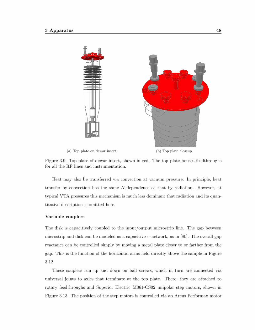
3 Apparatus 48
(a) Top plate on dewar insert. (b) Top plate closeup.
Figure 3.9: Top plate of dewar insert, shown in red. The top plate houses feedthroughsfor all the RF lines and instrumentation.
Heat may also be transferred via convection at vacuum pressure. In principle, heat
transfer by convection has the same N -dependence as that by radiation. However, at
typical VTA pressures this mechanism is much less dominant that radiation and its quan-
titative description is omitted here.
Variable couplers
The disk is capacitively coupled to the input/output microstrip line. The gap between
microstrip and disk can be modeled as a capacitive π-network, as in [80]. The overall gap
reactance can be controlled simply by moving a metal plate closer to or farther from the
gap. This is the function of the horizontal arms held directly above the sample in Figure
3.12.
These couplers run up and down on ball screws, which in turn are connected via
universal joints to axles that terminate at the top plate. There, they are attached to
rotary feedthroughs and Superior Electric M061-CS02 unipolar step motors, shown in
Figure 3.13. The position of the step motors is controlled via an Arcus Performax motor

3 Apparatus 49
(a) RF feedthroughs. (b) Feedthrough closeup.
Figure 3.10: RF feedthrough lines, shown in red. SMA-type couplers at the top plate areattached to 141-R transmission lines that, in turn, feed power to the disk resonator.
control unit and accompanying Labview software.
In adjusting the coupling to the disk resonator, the objective is a clear measurement of
Q0. Recall that∑
Pi from Equation 3.6 encompasses all the possible sources of power loss
in the system. Some of these Pi, such as RF losses from superconducting surface resistance,
are inherent properties of the resonator material. Other dissipative mechanisms, such as
lossy transmission lines or imperfect couplers, do not yield any information about the
disk resonator itself and should be neglected. These terms are incorporated into a new,
“loaded” QL. Then Equation 3.6 may be rewritten in a more suggestive form:
1
QL=
∑
i Pi
ωU(3.14)
=1
Q0+
1
Qin+
1
Qout+ · · · (3.15)
≡ 1
Q0
(1 + βin + βout + · · · ) (3.16)
(3.17)
where Qin and Qout represent power leaking out the resonator’s input and output couplers.

3 Apparatus 50
(a) Dewar insert shielding.
0 5 10 150
0.1
0.2
0.3
0.4
0.5
0.6
0.7
Shielding layersN
orm
aliz
ed h
eat t
rans
fer
(b) Normalized Q vs. N .
Figure 3.11: Thermal shielding plates, shown in red, reduce the radiative power transferbetween the room temperature environment above the top plate and the liquid heliumbath at the bottom of the dewar.
(The ellipsis indicates other sources of loss.) The βi are coupling constants, used to
characterize the relative strength of the different loss mechanisms in a particular structure.
Assume that the possible loss sources now include power leakage from the input and
output couplers: Pin and Pout, respectively. Pout can be minimized by adjusting the
coupling platforms so that βout ≪ 1. That is, the output coupling strength is reduced
as far as is practical. The input coupler is adjusted to achieve “critical coupling”, where
βin = 1. Then Equation 3.14 gives1
QL
=2
Q0
(3.18)
and so Q0 can easily be inferred from direct measurements. Critical coupling is easily
observed on a polar plot of S11.
The action of the variable couplers was simulated using Microwave Studio. The height
d of the variable couplers above the disk/microstrip gap was varied to produce coupling
coefficients in the range 1 > βin ≥ 0, with βout ≪ 1. Figure 3.14 shows a polar plot of
S11 (magnitude and phase) for different values of d.

3 Apparatus 51
(a) Variable couplers and support. (b) Coupler closeup.
Figure 3.12: Variable couplers allow for adjustment of RF coupling during low-temperature testing. The surrounding structure serves as mechanical support.
Once the system is critically coupled, surface wave losses can be estimated. The total
normalized loss is 1−|S11|2−|S21|2 = 0.95. Microwave Studio separates this into “surface”
and “volume” losses [88]; surface losses depend on the RF surface resistance Rs, while
volume losses PV stem from the loss tangent tan δ in the various dielectric materials of
the resonator system and are calculated according to Equation 3.19:
PV = πf tan δǫ0ǫr
∫
|E|2∂V. (3.19)
Simulation then indicates that volume losses compose 37.1% of the total losses. Similarly,
the total unloaded Q from simulation is Qsim.0 = 1100. Assuming that dielectric and
surface wave losses are the only volume losses, the contribution to Q from surface waves
is estimated to be QSW ≈ 1800.
This allows an estimation of the input power required to generate a given magnetic
field strength under the disk resonator. Using Equations 3.8-3.9, as well as the above
calculations, the peak magnetic field vs. input power is shown in Figure 3.15.
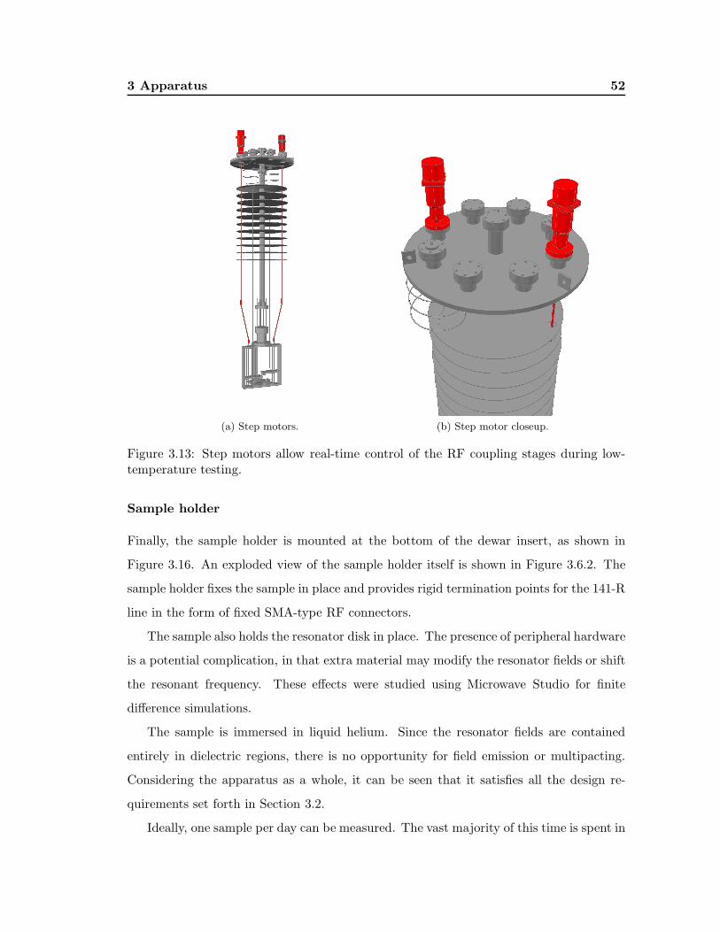
3 Apparatus 52
(a) Step motors. (b) Step motor closeup.
Figure 3.13: Step motors allow real-time control of the RF coupling stages during low-temperature testing.
Sample holder
Finally, the sample holder is mounted at the bottom of the dewar insert, as shown in
Figure 3.16. An exploded view of the sample holder itself is shown in Figure 3.6.2. The
sample holder fixes the sample in place and provides rigid termination points for the 141-R
line in the form of fixed SMA-type RF connectors.
The sample also holds the resonator disk in place. The presence of peripheral hardware
is a potential complication, in that extra material may modify the resonator fields or shift
the resonant frequency. These effects were studied using Microwave Studio for finite
difference simulations.
The sample is immersed in liquid helium. Since the resonator fields are contained
entirely in dielectric regions, there is no opportunity for field emission or multipacting.
Considering the apparatus as a whole, it can be seen that it satisfies all the design re-
quirements set forth in Section 3.2.
Ideally, one sample per day can be measured. The vast majority of this time is spent in

3 Apparatus 53
0.2
0.4
0.6
0.8
1
30
210
60
240
90
270
120
300
150
330
180 0
0.8 mm1 mm3 mm5 mm10 mm20 mm
Figure 3.14: Polar plot of S11 for various values of coupler stage height d. The radialcoordinate is |S11| and the angular coordinate in the phase, in degrees. Critical couplingis achieved for d = 0.8 mm, shown by the blue line.
0 5 10 15 20 25 30 35 40 450
20
40
60
80
100
120
140
160
180
200
Mag
netic
fiel
d (m
T)
Input power (W)
Figure 3.15: Peak magnetic field (mT) applied to the sample, as a function of input power(W).

3 Apparatus 54
(a) Sample holder. (b) Closeup.
Figure 3.16: The sample holder fixes the disk resonator in place, permitting the variablecouplers to function.
waiting for the dewar to warm after testing. Cooling to cryogenic temperatures typically
requires 1-2 hours, since the “small” dewars are used.

3 Apparatus 55
Figure 3.17: An exploded view of the sample holder, showing its several components. Thesame Nb disk and dielectric layer were used for every measurement.

Chapter 4
Thin films
The multilayer system in this work is composed of alternating thin films of niobium-
titanium nitride and aluminum oxide - (Nb,Ti)N and Al2O3. These films were deposited
in an ultra-high vacuum chamber via magnetron sputtering. The material properties of
these films are described below, along with the methods of deposition and an analysis of
the resulting material and superconducting properties.
4.1 Niobium-titanium nitride
(Nb,Ti)N was chosen for its specific superconducting properties. That is, it has a low value
of Hc1 and a high κ (see Section 3.5). It is also more mechanically and thermodynamically
stable at room temperatures, and is deposited at lower substrate temperatures than similar
superconducting nitrides [57,61]. Finally, Jefferson Lab has several facilities available for
the deposition of thin films via magnetron sputtering. For these reasons, (Nb,Ti)N is a
very suitable material for this work.
Niobium-titanium nitride has applications in the fields of SRF, astrophysics, and the
tool industry. It has been tested in SRF as a superconducting coating in elliptical copper
cavities [63, 95]. As discussed in Section 1.6, the idea here is to improve the thermal
conductivity, as well as the critical fields and temperatures of an elliptical cavity by using
thin films of materials other than Nb. Copper cavities with thin (Nb,Ti)N coatings tend to
have lower Q-values than bulk Nb cavities, and quench at lower gradients. (This is likely
due to the relatively high surface resistance of (Nb,Ti)N below 4.2 K.) The same material
is used in astrophysics for the fabrication of broadband THz mixers, used as components

4 Niobium-titanium nitride 57
in particle detectors [64, 96, 97]. The interest here is in thermodynamic stability, critical
temperature, and low shot noise. Finally, (Nb,Ti)N has a hardness similar to that of TiN
and is used to coat high-speed stainless steel cutting tools [98,99].
From a materials science perspective, niobium-titanium nitride is not very well un-
derstood, either in terms of phase stability or in terms of the structure-process-properties
relationship. The phase diagram of the Nb-Ti-N system is almost entirely unmapped.
Several sources give isothermal or isobaric sections of the phase diagram, as in Figure
4.1, but only at temperatures above 1200C [90,100,101]. Phase equilibrium data is un-
available at lower temperatures, likely because of the material’s refractory nature. More
recent works tend to focus on fabrication via reactive magnetron sputtering, but there is
no apparent effort made to establish whether the resultant phases are in equilibrium.
(a) Ternary phase isotherm at 1200C. (b) T vs. x for Nbx(TiN)1−x from 1200 to3000C.
Figure 4.1: The most complete Nb-Ti-N phase diagram available, reproduced from [100].The notation “78Bar” in the upper right of both is a citation referring to a work inGerman: R. Kieffer, H. Nowotny, P. Ettmayer and G. Dufek, Neue Untersuchungen uber
die Mischbarkeit von Uberganhsmetallnitriden und -karbiden. Metall, Berlin, 26, 701-708(1972).
Critical temperatures up to 18 K are achieved in (Nb,Ti)N by reactive diffusion of
nitrogen in Nb-Ti alloys [101]. However, as is typical of diffusion-based fabrication pro-
cesses, multiple phases and regions of stoichiometry coexist along the diffusion profile.
Furthermore, the accidental incorporation of oxygen has been difficult to avoid, given the
reactivity of both Nb and Ti [57,90,102,103]. The formation of various phases has been
correlated with the Nb/Ti ratio in the initial, un-nitrided sample [103]. Magnetron sput-

4 Niobium-titanium nitride 58
tering of thin films has the advantage of yielding fewer phases and less texture, depending
on substrate preparation. In contrast to bulk nitridation, sputtered thin films tend to
have critical temperatures in the range 12-15 K. This is likely the case because films
with nm-scale grains have a much shorter mean free path than the corresponding bulk
material. Magnetron sputtering is a more appropriate choice for the present work, since
a UHV sputtering system already exists at Jefferson Lab, and because the temperatures
required for reactive diffusion (& 1300C) are above the melting point (1085C) of some
copper system hardware.
The literature tends to be vague regarding the crystal structure of (Nb,Ti)N. Many au-
thors make no attempt at any crystallographic analysis whatsoever, but only empirically
relate the process conditions to the resulting critical temperature. Deposition processes
are therefore optimized for this single parameter and no other analysis is done. This is
especially true for SRF and astronomy applications, in which the end goal is a complicated
device with many fabrication steps. The most explicit statement about the crystal struc-
ture of (Nb,Ti)N seems to be that it is a cubic, NaCl type1 crystal structure, in which Nb
and Ti form a substitutional solution with random occupation of metal sublattice sites,
while N atoms occupy the nonmetal sublattice [91, 98, 100, 104]. The NaCl structure is
maintained over a range of stoichiometries Nb1−xTixN [61,92,99].
Pure niobium nitride is itself a candidate for SRF thin films: its cubic NaCl-type
phase (referred to as the δ phase) has a critical temperature of approximately 16 K
[105,106]. However, at temperatures below 1300C the δ phase exists over a narrow range
of nitrogen concentrations. Outside that range, the tetragonal γ-Nb4N3 and hexagonal,
non-superconducting ǫ-NbN phases may also form, resulting in films with lower critical
temperatures [101,107]. The Nb-N phase diagram is reproduced in Figure 4.2 from [108].
By contrast, the cubic δ phase of TiN is quite stable, existing over a wide range of
temperatures and nitrogen concentrations but with a very low critical temperature, closer
to 5 K [90]. The Ti-N phase diagram is shown in Figure 4.3. It seems that adding
titanium to the Nb-N system2 beneficially stabilizes the NaCl crystal structure at lower
1This is sometimes referred to as a B1 structure.2As an alternative to Ti, some groups stabilize the δ-NbN phase by adding carbon [111]. This can be
accomplished by introducing small amounts of CH4 (around 2%) to the Ar/N2 gas [105].

4 Niobium-titanium nitride 59
Figure 4.2: The Nb-N binary phase diagram, reproduced from [108]. According to Zhito-mirsky et al., the δ phase is formed in the black shaded region [107]. However, this seemstopologically impossible in a binary phase diagram [109]. A more likely interpretationis that δ-NbN is formed in the region between approximately 48 and 50 atomic percentnitrogen. While this is a narrow range of compositions, δ-NbN is not evidently unsta-ble at low temperature. This is supported by data in the ICDD Powder Diffraction File(04-004-2895, 04-004-2918) [110].

4 The UHV system 60
Figure 4.3: The Ti-N binary phase diagram, reproduces from [108]. The δ-TiN phase isshown at the right of the diagram, for temperatures up to 3290C and compositions of>30 atomic percent N.
temperatures while retaining a high superconducting critical temperature [90,101]. This
phenomenon is supported by the data presented below. But first, a discussion of the
methods of film production is appropriate.
4.2 The UHV system
(Nb,Ti)N films were deposited by DC reactive sputtering of a Nb0.7Ti0.3 target in a
nitrogen environment. This process was performed in a vacuum chamber capable of
reaching base pressures of 10−9 Torr - the ultra-high vacuum (UHV) range. This chamber
was first discussed by Valente-Feliciano et al. in [112]. As the chamber was assembled
in-house, its layout and operation will be discussed below. This section also discusses the
process by which (Nb,Ti)N and Al2O3 films are deposited. Lastly, the chamber is still in
its commissioning phase. The deposition process is still being refined, and modifications
will be made to the process and the system hardware for months to come. Potential
modifications to the system will be discussed at the end of this section.

4 The UHV system 61
4.2.1 The deposition chamber
A drawing of the UHV chamber is shown in Figure 4.4, along with the make and model of
its various components. A simplified schematic is shown in Figure 4.5. The main chamber
is bell-shaped, roughly 1.5 m high. The chamber is opened via a mechanical hoist, which
lifts the upper section straight up. A 26-inch Wheeler flange joins the two sections, sealed
with a Viton gasket.
As is typical, the chamber is evacuated in stages. Once the chamber is sealed, a
scroll pump brings the pressure to approximately 30 mTorr. During this stage, a UVB
lamp is switched on to encourage desorption of contaminants from the chamber walls.
Below 30 mTorr, the scroll pump is valved off and a gate valve is opened between the
main chamber and a 14-inch diameter cryopump. The chamber pressure quickly drops to
10−7 Torr, and after 24 hours of pumping will reach the 10−9 Torr range. An ion gauge
monitors chamber pressure during this stage.
A residual gas analyzer (RGA) monitors impurities in the chamber and is used for
helium leak checks. As in Figure 4.5, the RGA is connected to the chamber in two ways:
by a six-inch VAT UHV gate valve and by a narrow, valved, bypass conductance. The
bypass conductance keeps the RGA functioning at low (∼ 10−6 Torr) pressures, even
when the main chamber at process pressures of ∼ 2 mTorr. Process gasses are introduced
via variable leak valves. Since the chamber is still in its commissioning phase, there is not
currently a mass flow controller to regulate, e.g., partial pressures of N2 vs. Ar. In lieu
of a mass flow controller, partial pressures are controlled by manually adjusting the leak
valves while reading the RGA output. This method allows regulation of partial nitrogen
pressure to within roughly 10%.
Three AJA magnetrons (model A320) are installed at the base of the chamber. They
are all are water-cooled and can be used for both DC and RF magnetron sputtering. An
Advanced Energy MDX-1K DC power supply is used for DC sputtering. RF power is
provided by an Advanced Energy RFX-600 RF generator, coupled to the magnetron guns
via an RF matching network (Seren MC-2, AT-10). The matching network is composed of
two variable vacuum shunt capacitors, bridged by an inductor. The capacitors are auto-
matically adjusted to match the chamber’s plasma load to the RF generator impedance,

4 The UHV system 62
ensuring that minimal power is dissipated in the power cables (RG-393), the chamber
walls, etc.
The chamber is housed in a cleanroom. All components installed in the system are
first de-greased in an ultrasonic bath of Micro 90, an industrial detergent, followed by
ultrasonic baths in various solvents. Copper components are additionally given an acid
etch (55% phosphoric acid, 20% nitric acid, 25% acetic acid) in order to remove oils and
other contaminants from the surface. These precautions help to ensure the purity of
deposited films, and their regular practice helps ensure process control.
4.2.2 The sample holder
To ensure adequate film uniformity during reactive sputtering of NbTiN, a heated sample
holder was constructed. A schematic is shown in Figure 4.6. The eight-inch CF flange is
mounted horizontally into the UHV system at position “G” in Figure 4.4. The sample
holder has several functions: it fixes the sample in place, provides uniform heating across
the sample, and serves as a guide for a pattern mask (whose function is discussed below).
The design also accommodates several chamber requirements. For example, the sample
holder is mounted in a horizontal, 8-inch CF flange because all other work performed in
the UHV system is mounted similarly.
The sample is bolted to the front of an OFHC copper heater block. The block is a
cylinder, 12.7 cm in diameter and 6.35 cm long. The rear of the heater block, which is
always under atmospheric pressure, houses sockets for a cartridge heater and a thermo-
couple for heating and temperature control.
A Waltow“Firerod” 500 W cartridge heater is inserted into a socket on the rear of
the heater block. A K-type thermocouple mounted in the cylinder provides feedback for
temperature control. Temperature regulation is handled via a Fuji Electronic Systems
PXR-9 temperature controller, which opens and closes an Omron G3NA-210B solid state
relay connected to 240 V AC. That wall-plug power drives the cartridge heater.
The main concern in designing the heated sample holder was the thermal gradient
across the sample. This is complicated by the size of the sample substrate: 8×10×0.6 cm.
(Although the disk resonator itself is only 4 cm in diameter, accommodating the microstrip

4 The UHV system 63
AB
C
D E F
G H
KL
M
Figure 4.4: UHV chamber drawing. (A) Chamber; (B) Chamber hoist & support; (C)Instrumentation, control, RF/DC power supply; (D) N2, O2, Ar, Kr gas inputs (Varianvariable leak valves); (E) Oscillator (Sycon OSC-100A), coupled to Sycon STM-100 thick-ness monitors; (F) Granville-Phillips 275 convection gauge; (G) 8” and 6” conflat portsfor heater and shutter; (H) view port; (K) AJA Int’l. A320 magnetron guns, with coolantand power supply lines; (L) Itawa 5700 scroll pump; (M) UVB lamp. NOT SHOWN:Granville-Phillips Stabil-Ion process ion gauge; CTI Cryo-Torr 10 14” cryo-pump; VATgate valve; Pfeiffer TMU-071 turbopump, residual gas analyzer (Pfeiffer Prisma 80).

4 The UHV system 64
Figure 4.5: Simplified UHV chamber block diagram.

4 The UHV system 65
(a) Front view (chamber side).
(b) Rear view (atmosphere side).
Figure 4.6: Heated sample holder schematic.

4 The UHV system 66
Cu stage radius (m)
Temperature Gradient (K/m)
Cu
stag
e he
ight
(m
)
0.06 0.065 0.07 0.075 0.08 0.085 0.09 0.095
0.08
0.085
0.09
0.095
0.1
0.105
0.11
0.115
0.12
0.125
−2.4
−2.2
−2
−1.8
−1.6
−1.4
−1.2
Figure 4.7: Thermal gradient across sample for various sizes of heater. No reasonablechoice of heater dimensions results in a gradient of more than a few Kelvin.
input and output couplers requires a larger substrate.) The temperature of the substrate
must be uniform across its face to within a few Kelvin. This is verified by integrating
Fourier’s law for heat conduction
Q = −kAdT
dr,
where r is the radial coordinate, Q is the rate of heat transferred to the copper cylinder,
k = 401 W/m·K is the thermal conductivity of copper, A is the area normal to the heat
flux (which in this case varies with r), and T is temperature.
The heater block is modeled as a uniform cylinder with length ℓ and an outer radius
r2. A hole of radius r1 is drilled through the center to accommodate the cartridge heater.
Integrating in cylindrical coordinates gives the thermal gradient across the heater face as
∆T = −Q ln(r2/r1)
2πkℓ.
For reasonable values of r2 and ℓ, with r1 = 1.9 cm, the thermal gradient is shown in
Figure 4.7. Evidently, any reasonable choice of cylinder dimensions will give negligible
thermal gradient across the sample.
In preparation for deposition, the heater block is brought to 600C and kept at that
temperature for four hours. This heat treatment stimulates desorption of impurities from

4 The UHV system 67
the sample and facilitates the transition from the high vacuum regime at 10−7 Torr to
the UHV regime at 10−9 Torr.
4.2.3 Magnetron sputtering
Deposition begins once the chamber has been evacuated to UHV pressures, a helium leak
check has been performed, and the substrate has been held at 600C for some time. At that
point, the sputtering gas is introduced and the gas pressure is adjusted as described above.
(Nb,Ti)N films are reactively sputtered so the ratio of partial pressures P(N2)/P(Ar)=0.15
for an overall process pressure of 2 mTorr3, as measured by an ion gauge.
For both (Nb,Ti)N and Al2O3 films, the sputtering target is covered with a movable
shutter. The target face is then conditioned for thirty minutes. That is, a plasma is
struck and the target is sputtered for some time to remove impurities and stabilize the
temperature at the target face. The mask ensures that no sputtered particles reach the
substrate before the system is in equilibrium.
Sputtering of (Nb,Ti)N films
As mentioned above, (Nb,Ti)N films are formed by reactively sputtering a Nb0.7Ti0.3
target in an N2/Ar gas mixture. The plasma is lit with 60 W DC power from a power-
stabilized ENI DCG-100 generator, designed for plasma operation. The power is then
ramped to 300 W, corresponding to 0.88±0.01 A and 340±5 V at the cathode. Power
stabilization, as well as the ensuing stability of cathode voltage and current settings,
support an equilibrium deposition rate.
For “good” films, these gas and cathode settings give a deposition rate of 16.0±0.3 nm/min
as measured afterward with a profilometer. Although there are two thickness monitors
mounted in the deposition chamber, these are used mainly for qualitative assessments of
sputter conditions. That is, plasma density varies with distance from the target face, so
meaningful quantitative measurements with thickness monitors are only possible if they
obstruct the path between the target and the substrate. As an alternative, trial films were
deposited on a-plane sapphire substrates (single crystals, polished to 90 A mean surface
3Since an RGA is used in lieu of a mass flow controller, it is more accurate to say that “15%” describesthe ratio of ion currents in the RGA chamber. The partial pressures are inferred, but not measureddirectly.

4 The UHV system 68
roughness, with ∼1 cm2 surface area) and the thickness of these films was measured later
using a profilometer. Similarly, during deposition on the large, 8×10 cm substrates used
for the disk resonators, sapphire witness samples were used to perform post-facto analysis
of superconducting and surface properties; the full-size samples are too large and heavy
to fit in, e.g., a diffractometer.
Those small sample measurements, then, form the basis for all statements of thickness
and deposition rate. Film thickness is controlled, then, by controlling the partial gas
pressures and timing each deposition according to the above-stated deposition rate. Ex-
cluding target conditioning, it takes approximately 9 minutes and 20 seconds to deposit
150 nm of (Nb,Ti)N. At the end of the deposition window, the target shutter is replaced
and the gas and magnetron power are switched off.
Sputtering of Al2O3 films
Alumina films are formed by RF magnetron sputtering of an alumina target in an Ar
plasma. The plasma is lit with 65 W, 13.56 MHz RF power, at gas pressures above
8 mTorr. Once the plasma is lit, the forward power is ramped slowly to 120 W, beyond
which there is no appreciable change in the deposition rate. The working Ar pressure is
held as low as is reliably possible (roughly 0.8 mTorr) to maximize the mean free path
of sputtered particles and to keep the cryopump temperature stable. After the matching
network is tuned, most of the forward power is delivered to the magnetron and only 1-3 W
are reflected back. Deposition rates are characteristically low for the RF sputtering of
alumina: approximately 1.2 nm per minute.
Al2O3 was chosen because it was readily available as a dielectric target material; as
polished substrates for the creation of small samples; and as bulk, 2 mm sheet for the thick
dielectric layer under the disk resonator. Using the same material for all three purposes
simplifies multilayer analysis. However, there is a noteworthy complication. The best
alumina films - that is, the films with the highest dielectric constant and breakdown volt-
age - are those in which alumina is deposited via reactive sputtering in an argon/oxygen
mixture [113–115]. The presence of oxygen in the Nb-Ti-N system would form oxide com-
pounds in the superconducting layers via reactive diffusion, with an oxidation rate on the

4 Film analysis 69
order of 1 mg/cm2h [116, 117]. This is an unacceptable contamination that could result
in lower Tc values via, for example, N→O substitution in the lattice [118].
After deposition, all samples are held at 600C for several hours and then cooled over
a period of 12 hours at UHV pressures. The small samples’ surface and superconducting
properties can then be studied directly, while the resonator substrates can be prepared
for multilayer analysis.
4.3 Film analysis
Film analysis falls into two broad categories. Superconducting properties are studied
chiefly by DC measurements of the critical temperature Tc. Assessments of crystal struc-
ture and surface properties are made using a suite of surface-analytical tools available at
Jefferson Lab: profilometry, atomic-force microscopy (AFM), energy dispersive x-ray spec-
troscopy via scanning electron microscope (SEM-EDS), and x-ray diffractometry (XRD).
The results of these studies are presented here.
The goal of this work is the development of an experimental program for multilayer
film analysis. As such, a complete determination of the crystal structure of (Nb,Ti)N was
not undertaken. However, there are several conclusions about crystal structure that were
be made in the course of structural analysis for the sake of process refinement.
4.3.1 Tc measurements
The superconducting properties of thin films may be assessed and compared most conve-
niently at Jefferson Lab via simultaneous measurements of the critical temperature, Tc,
and the residual resistivity ratio, RRR. This is accomplished via the standard four-point
probe analysis [119–121]. Four parallel, spring-mounted, gold-plated probes are placed
in contact with a sample film. The two outer probes (see Figure 4.8) supply a known
DC current, while the two inner probes measure the subsequent induced voltage. The
resistivity can then be measured.
The apparatus is placed in a dewar in the VTA and cooled to cryogenic temperatures.
Then a heater in the dewar slowly warms the test apparatus so that resistivity can be
measured between 2 and 300 K, typically at intervals of 0.1 K over a period of roughly

4 Film analysis 70
Figure 4.8: Cartoon showing four-point probe configuration for Tc and RRR measure-ments. Current leads I and voltage leads V are shown.
12 hours. The transition between the superconducting and normal states is indicated by
a sharp increase in the measured DC resistivity, as shown in the figures below.
Process development for (Nb,Ti)N films in the JLab UHV system is still underway.
Maximizing Tc and film uniformity is an ongoing part of chamber commissioning. For the
purposes of this thesis, it is sufficient to determine a chamber state that will repeatably
produce films with values of Tc comparable to those found in the literature for similar
substrates and deposition methods. The chamber state is found empirically by depositing
and characterizing a wide range of thin films under varying deposition conditions.
The nitrogen partial pressure during deposition strongly influences the superconduct-
ing properties of the resulting films. A subset of the film data is presented, then, in
two groups. One group, “Group A”, shows the influence of partial nitrogen pressure on
film characteristics. Three Group A films are referenced below to illustrate differences
resulting from nitrogen partial pressure P (N2): Sample 01 (P (N2) =10%), Sample 02
(P (N2) =15%), and Sample 03 (P (N2) =5%). Another group, “Group B”, is composed of
films deposited under nominally identical conditions and showing similar, relatively high
values of Tc. The Group B films represent some degree of process control and repeatability.
Tc and RRR measurements of both groups are shown in Figures 4.9a and 4.9b, respec-
tively. The net result is that for this experiment, Tc = 13.2± 0.5 K and RRR=1.46±0.58.
RRR is far more variable that Tc, suggesting relative control of stoichiometry (which
strongly influences Tc, see Section 4.1) but run-by-run changes in microstructure.

4 Surface analysis 71
5 10 15 20 25 300
50
100
150
200
250
300
Temperature (K)
Res
istiv
ity (
µΩ−c
m)
10% N
2
15% N2
5% N2
(a) Group A: Tc varies with P (N2).
5 10 15 20 25 300
50
100
150
200
250
300
Temperature (K)
Res
istiv
ity (
µΩ−c
m)
DB−04DB−05DB−06DB−07DB−08DB−09
(b) Group B: Tc = 13.2 ± 0.5 K.
Figure 4.9: Varying the partial nitrogen pressure during deposition results in widelyvarying superconducting parameters. Figure 4.9a shows Group A films: Sample 01 (blue,10% P (N2)), Sample 02 (red, 15%), and Sample 03 (green, 5%). Sample 03 has a transitiontemperature below 5.6 K. Group B results are comparable to those found in [63], e.g.Figure 4.9b shows data for six films, all deposited under nominally identical conditionsand demonstrating the repeatability of creating films with Tc ≈ 13 K.
4.4 Surface analysis
Apart from superconductivity, in order for films to be useful for the analysis and interpre-
tation of multilayer structures, they must be smooth and their thickness must be known.
A smooth film ensures a clean interface between superconducting and insulating layers,
with no pinholes or shorts between conducting layers. It also drastically simplifies the vor-
tex image problem, so that the calculations from Chapter 2 might still apply. And in order
to have any a priori understanding of Q or Hv in a multilayer resonator, the film thickness
must be known. Atomic force microscopy (AFM) and profilometry measurements were
conducted to address these issues. The results are discussed below.
The present work is the beginning of a long-term multilayer film study in which
(Nb,Ti)N will have a nontrivial role. To the extent that the deposition process may
be better understood, both for this and for future analyses, some further amount of mate-
rial characterization is useful. To this end, x-ray diffraction (XRD) and energy-dispersive
x-ray spectroscopy (EDS) measurements were conducted, and are discussed below.
All surface analysis was conducted on small samples. As discussed in the previous
section, there are two groups of samples. In the first group, Group A, the partial nitrogen

4 Surface analysis 72
pressure was varied during deposition Samples made at three different values of P (N2)
give a rough idea of the influence of sputter conditions on film structure. In the second
group, Group B, samples were deposited with the goal of uniformity and repeatability,
resulting in critical temperatures of 13.2±0.5 K. Group A is used to show the effects of
varying deposition conditions on the resulting film structure. Group B is used to discuss
the general properties of (Nb,Ti)N.
It is worth stating explicitly that more measurements must be made on more samples
before any sound, statistical conclusions can be drawn. The results presented below form
the basis for qualitative analysis.
4.4.1 Thickness measurements
Measurements of film thickness were made using a Dektak 3ST surface profiler. Small
samples are clipped to the heater block. The clip masks part of the sample substrate,
creating a step in the film height which can then be measured. A stylus, scanned across
the step, records the change in film height. Multiple scans across each step give the results
shown in Figure 4.10.
The samples in Figure 4.10b were made under varying partial nitrogen pressures, but
with equal deposition time. This variable deposition rate may be influenced by the reac-
tion of nitrogen with the target surface. A partial nitridation of the target would lower
both the sputtering yield and the secondary electron emission coefficient[122]. Further-
more, the cross section for ionization of N2 by electrons is 40% lower than that of Ar,
leading to a reduced ion density in the plasma [123]. As stated above, films in Group B
have deposition rates on the order of 16 nm/min.
4.4.2 AFM
Recall from Chapter 2 that the Gurevich model of vortex behavior in a multilayer struc-
ture is dependent on a smooth interface between film layers. Quantifying the RMS surface
roughness is then one way of evaluating multilayer films. Root meas square (RMS) sur-
face roughness measurements were conducted using a Digital Electronics scanning probe
microscope in tapping AFM mode. Data from each sample reflects three separate mea-
surements, each taken over an area of 25.30±0.11 µm2. Typical results are shown in

4 Surface analysis 73
(a) Dektak 3ST sample output.
4 6 8 10 12 14 16 18450
500
550
600
650
700
750
800
850
900
Film
thic
knes
s (n
m)
Partial nitrogen pressure (%)
(b) Thickness vs. P (N2).
Figure 4.10: Measurements of film thickness for samples under varying deposition condi-tions, but equal deposition time.
Figure 4.11. RMS surface roughness as a function of partial nitrogen pressure is shown
in Figure 4.12. The RMS surface roughness is then on the order of 1 nm for films up
to 800 nm thick. From Figures 4.11b and 4.11d, the lateral length scale is estimated4 to
be on the order of 50 nm. There are several mechanisms contributing to the surface
roughness shown in Figures 4.12 and 4.10. It is well-known that films deposited via mag-
netron sputtering (i.e. with limited adatom mobility) tend to have small grain sizes with
irregular columnar morphologies. Consider the Thornton zone structure model, developed
from earlier work by Movchan and Demchishin, which qualitatively relates morphology to
homologous deposition temperature5 and sputtering gas pressure [124]. From Figure 4.2,
the homologous temperature during deposition T/Tm ≈ 0.25 suggests small, columnar
grains with grooved, metallurgical boundaries. Such grains grow slowly during deposi-
tion, resulting in conical grain structures. Given the estimated lateral length scale of
∼50 nm discussed above, this morphology suggests 50 nm as a rough grain size at the
film surface. In addition, the random deposition of particles may lead to roughening via
kinetic processes [125]. Given that surface roughness and grain boundary density have an
effect on the behavior of magnetic flux vortices, this suggests avenues for further study.
That is, an increased grain size could result in increased surface roughness, suggesting a
4Unfortunately, the original AFM data files could not be recovered, precluding a more precise mea-surement of lateral length scales via power spectral density analysis, e.g.
5“Homologous” refers to material temperature T normalized to its melting temperature Tm.

4 Surface analysis 74
(a) AFM on Sample 02. (b) 3D view.
(c) AFM on Sample 03. (d) 3D view.
Figure 4.11: 25 µm2 AFM scans of Sample 02 (Tc=13 K) and Sample 03 (Tc < 5.6 K),showing a uniform surface.
compromise between the two might be necessary.
4.4.3 Further analysis
Composition and phase studies have also been conducted using XRD and SEM-EDS. A
full crystallographic analysis of (Nb,Ti)N will be conducted after the UHV chamber is
fully commissioned and the deposition process has been further refined. However, several
conclusions can be drawn at this preliminary stage.
First, standardless FAZ component analysis [126] was conducted using an EDAX

4 Surface analysis 75
0.04 0.06 0.08 0.1 0.12 0.14 0.16 0.18
0.7
0.8
0.9
1
1.1
1.2
1.3
1.4
1.5
Partial nitrogen pressure (%)
Mea
n su
rfac
e ro
ughn
ess
(nm
)
(a) Group A RMS surface roughness vs. P(N2).
450 500 550 600 650 700 750 800 850 900
0.7
0.8
0.9
1
1.1
1.2
1.3
1.4
1.5
Film thickness (nm)
Mea
n su
rfac
e ro
ughn
ess
(nm
)
(b) RMS surface roughness vs. thickness.
Figure 4.12: RMS surface roughness data for Group A samples 01-03, showing a trendtowards roughness as films increase in thickness. Since these films were all deposited atdifferent nitrogen partial pressures, a clear determination of the dependence of roughnesson film thickness is difficult.
SEM-EDS system. A typical x-ray emission spectrum (Figure 4.13) shows the films to be
quite clean. That is, the films are composed primarily of nitrogen, niobium, and titanium.
There is evidence for carbon contamination in a small minority of samples, explained by
the solubility of carbon in transition metal nitride systems [99]. Hydrogen and oxygen are
also likely contaminants. However, SEM-EDS is ineffective for elements with Z ≤ 4 and
so insensitive to hydrogen, and the presence of oxygen in the sample substrates makes
its detection in the film impossible. Compound identification via X-ray photoelectron
spectroscopy is therefore a likely next step in material analysis.
X-ray diffraction studies were performed using a Panalytic X’Pert Pro four-circle
diffractometer. θ − 2θ measurements in the Bragg-Brentano geometry (Figure 4.14) sug-
gest a B1 configuration, as discussed above. Coherent reflections are evident for “un-
mixed” Miller indices, from which a lattice parameter a0 = 4.3 A is calculated. Only
the [111] and [200] orientations are visible. A high degree of disorder is suggested as well,
since these peak intensities are quite low compared with that of the sapphire substrate. A
natural degradation of intensity with increasing θ may be the reason why no peaks were
visible above 2θ ∼ 45 [127].
Data from the ICDD6 powder diffraction file (PDF, Reference [110]) are compared
6International Centre for Diffraction Data. http://www.icdd.com

4 Surface analysis 76
0 1 2 3 4 5 6
Energy (keV)
Nb (Lα1) + Nb (Lβ
1)Nb
(Lγ2)
Nb(Mα
1)
Ti (Kα1) Ti (Kβ
1)Al (K α
1)N (Kα
1)
log(
Cou
nts)
DB−01DB−02DB−03
Figure 4.13: EDS peak intensity vs. critical emission energy (keV) for Group A. Only N,Nb, Ti are present - film contamination is atypical. The “shoulder” on the Nb Mα1 peakis likely from C Kα.
35 36 37 38 39 40 41 42 43 44 4510
0
101
102
103
104
105
2θ
Inte
nsity
DB−01DB−02DB−03
Figure 4.14: Bragg-Brentano XRD scan for samples in Group A. The prominent centerpeak is created by the sapphire substrate.

4 Surface analysis 77
with Group A data in Figure 4.15. In particular, diffraction peaks from the possible cubic
phases of the Nb-N and Ti-N systems are shown. A comparison of 2θ-values for these
phases strongly suggests that δ-(Nb,Ti)N is indeed formed during reactive sputtering.
As previously stated, SEM-EDS measurements suggest the predominance of Nb, Ti,
and N in the films used for this work. Figure 4.15 shows the relationship between the
structure of those films and that of the various δ phases that are possible in the Nb-
Ti-N system. Of course, there are other, non-cubic phases possible given the deposition
temperature. Figure 4.16 compares PDF x-ray diffraction spectra [110] for various non-
cubic phases of the Nb-Ti-N system. Again, the location of diffraction peaks strongly
suggests the formation of δ-(Nb,Ti)N films.
Figure 4.17a shows a closeup of the (111) peak from Figure 4.14. The 2θ value is
compared with those of ideally stoichiometric NbN and TiN [128, 129]. The lattice pa-
rameter of (Nb,Ti)N therefore seems to be a compromise between those of NbN and TiN,
also shown in Figure 4.15. The lattice parameter also seems to vary with the relative
concentrations of Nb and Ti. However, SEM-EDS composition data empirically show no
substantial variation in Nb-Ti relative composition. Then (Nb,Ti)N does not appear to
follow Vegard’s law [130], so plots like Figure 4.17c do not trivially yield composition
data. Variations in the lattice parameter a0 are likely due to a combination of film stress
and nitrogen partial pressure.
The XRD peaks for Group B samples tend to be quite broad and of low intensity,
compared with those measured by other groups [90, 120]. The low intensity is likely due
to very small grain size. A rigorous study of grain size in (Nb,Ti)N films will require
measurements made using a transmission electron microscope. Absent such a set of mea-
surements, a rough estimate of grain size can be made from the width of diffraction peaks.
Specifically, the Scherrer equation [131] relates the full width at half maximum (FWHM)
of a diffraction peak to the width β of a crystallite:
FWHM =Kλ
β cos θ. (4.1)
Here, λ = 0.154 nm is the x-ray wavelength (Cu Kα), θ is the Bragg diffraction angle, and
K is a dimensionless factor of order 1, determined by the grain shape. Using the peak
widths in Figures 4.17a and 4.17b, and assuming a spherical grain shape (K ≈ 1.3), the

4 Surface analysis 78
35 36 37 38 39 40 41 42 43 44 45
2θ (degrees)
Inte
nsity
(ar
bitr
ary
units
)
δ−TiN*
P(N2)=0.05
P(N2)=0.10
P(N2)=0.15
δ−(Nb,Ti)N*
δ−NbN0.9
*
δ−NbN0.98
*
Figure 4.15: Bragg-Brentano x-ray diffraction spectra for Group A films deposited atvarious partial nitrogen pressures, compared with PDF data for other possible cubicphases: δ-TiN (PDF 00-038-1420), δ-Nb0.5Ti0.5N (PDF 01-089-5134), δ-NbN0.9 (PDF 04-004-2918), and δ-NbN0.98 (PDF 04-004-2895). In the plot, an asterisk (e.g. “δ-TiN∗”)indicates a diffraction spectrum that was obtained from the ICDD powder diffraction filerather than measured directly. There is a gradual shift in 2θ values between stoichiometricTiN and NbN peaks, with δ-(Nb,Ti)N peaks in the middle. The strong peak at 2θ = 37.8
for the Group A films originates from the a-plane sapphire substrates.

4 Surface analysis 79
35 36 37 38 39 40 41 42 43 44 45
2θ (degrees)
Inte
nsity
(ar
bitr
ary
units
)
α−Nb (bcc)
α−Ti (hcp)
β−Nb2N (hcp)
γ−Nb4N
3 (tet)
δ−(Nb,Ti)N
δ−(Nb,Ti)N (meas.)
Ti2N (tet)
Figure 4.16: Bragg-Brentano x-ray diffraction spectra for deposited films (shown in red)compared with PDF spectra for δ-Nb0.5Ti0.5N (PDF 01-089-5134), α-Nb (PDF 00-034-0370), α-TiN (PDF 00-044-1294), β-Nb2N (PDF 00-039-1398), γ-Nb4N3 (PDF 01-089-5132), and Ti2N (PDF 04-007-0773). The abbreviation “bcc” indicates a body-centeredcubic phase, “hcp” indicates hexagonal, and “tet” indicates tetragonal. The measureddiffraction peaks correspond closer to the δ-(Nb,Ti)N phase than to any other accessible,non-cubic phase of the Nb-Ti-N system.

4 Surface analysis 80
Scherrer equation gives a grain size between 30 and 50 nm, in rough agreement with the
estimates from AFM discussed above. Note that Equation 4.1 represents a lower bound
on grain size. Other phenomena, such as inhomogeneous film strain, can also contribute
to peak broadening [127]. Small grain sizes result in a high density of grain boundaries,
which can in turn influence the behavior of flux vortices in the film. Specifically, vortices
may penetrate a superconductor at lower magnetic fields than in equivalent single-crystal
material [132].
Eventually, the experimental system described in Chapter 3 will be used to accumulate
a statistically large amount of data, such that concrete conclusions may be made concern-
ing (Nb,Ti)N film composition and its effect on superconducting behavior. In addition,
the commissioning of the UHV system (Section 4.2) will involve small (Nb,Ti)N samples
made under a variety of deposition conditions. For example, it is not now clear where the
maximum lies in the relationship between partial nitrogen pressure and Tc, from Figure
4.9a. The qualitative observations made in this section suggest directions of inquiry for
future work in (Nb,Ti)N process development.

4 Surface analysis 81
35 35.2 35.4 35.6 35.8 36 36.2 36.4 36.6 36.8 370
200
400
600
800
1000
1200
2θ (degrees)
Inte
nsity
(cp
s)
NbN (111)TiN (111)data
(a) Closeup of 111 peak, Group B.
41 41.2 41.4 41.6 41.8 42 42.2 42.4 42.60
5
10
15
20
25
30
35
40
45
50
2θ (degrees)In
tens
ity (
cps)
NbN (200)TiN (200)data
(b) Closeup of 200 peak, Group B.
0.42 0.422 0.424 0.426 0.428 0.43 0.432 0.434 0.436 0.438 0.4410
0
101
102
103
104
Lattice parameter (nm)
Cou
nts
P(N
2)=0.1
P(N2)=0.15
P(N2)=0.05
(c) a0 varies with partial N2 pressure.
Figure 4.17: Plots of the (111) and (200) peak for various samples, giving informationabout the lattice parameter a0. The gray band in Figures 4.17a-4.17c represents the rangeof a0 values given in [100].

Chapter 5
Preliminary RF measurementsand conclusions
This dissertation has presented an experimental program to evaluate multilayer films
for SRF. Preliminary results are presented here, and the RF measurement apparatus is
described. Finally, since the present work represents the start of a long-term analysis,
plans are discussed for modifications and improvements to the apparatus.
The measurements discussed in this chapter demonstrate a proof of principle. The
resonator works at its design frequency, the measured Q is close to predicted values,
and the variable couplers can be manipulated to obtain critical coupling, as discussed in
Section 3.6.2.
5.1 RF measurement apparatus
It is often the case that measurements of SRF cavities require special hardware for fre-
quency stabilization of RF power sources. A cavity with Q0 ∼ 109 may have a bandwidth
on the order of 1 Hz. In that case, slight changes to the cavity from vibration or elec-
tromagnetic field pressure are enough to move the cavity off-resonance. For example, the
VTA at Jefferson Lab uses phase-locked loops to correct the forward RF power in real
time, constantly adjusting the frequency to compensate for any detuning effects.
By contrast, the disk resonator has a calculated bandwidth ∆f = f/2Q0 = 1.3 MHz.
Operation at resonance is therefore stable, and can be maintained simply by using a vector
network analyzer (VNA) as a source of RF power. The low output power (< 10 mW) of

5 RF measurement apparatus 83
the VNA is amplified through a 34.4 dB S-band traveling-wave tube amplifier (TWTA),
which nominally provides up to 25 W forward power to the resonator. The configuration
of this and other assorted RF hardware is shown in Figure 5.1. Note that, at the time RF
measurements were conducted, it was not possible to calibrate the VNA. Measurements
of Q, S11, and S21 therefore include all sources of loss between the ports of the network
analyzer. Measurements with a Hewlett-Packard 437B RF power meter show that, in
Figure 5.1: Schematic of RF measurement setup. Counter-clockwise from the top, thecomponents are: an Agilent E5071C four-port vector network analyzer; a Varian VZS6951K1D traveling wave tube amplifier (2-4 GHz, 34.4 dB gain); a UTE Microwave Inc.CT-3041-N circulator (2-4 GHz); a Narda 367NM 50Ω load (2-18 GHz, 40 W max.); thedewar insert described in Chapter 3; and a Narda 769-30 -30 dB attenuator (DC to 6GHz, 150 W max.).
practice, the TWTA saturates at a maximum of 20 W output power 1. This is likely
because the amplifier is almost 20 years old. Between 14 and 20 W, there is a nonlinear
region in which the amplification falls from the nominal 34.4 dB. In this nonlinear region
the TWTA can generate harmonics, exciting higher-order modes in the resonator. These
first measurements of the control resonator were therefore made in the linear region, below
14 W output power.
1The power sensor used with the 437B has a maximum input power of 300 mW. The measurements ofoutput power were therefore made by inserting a Narda 769-30 S-band attenuator in between the amplifierand the power meter. At 2.75 GHz, the 769-30 has an attenuation of -29.8 dB.
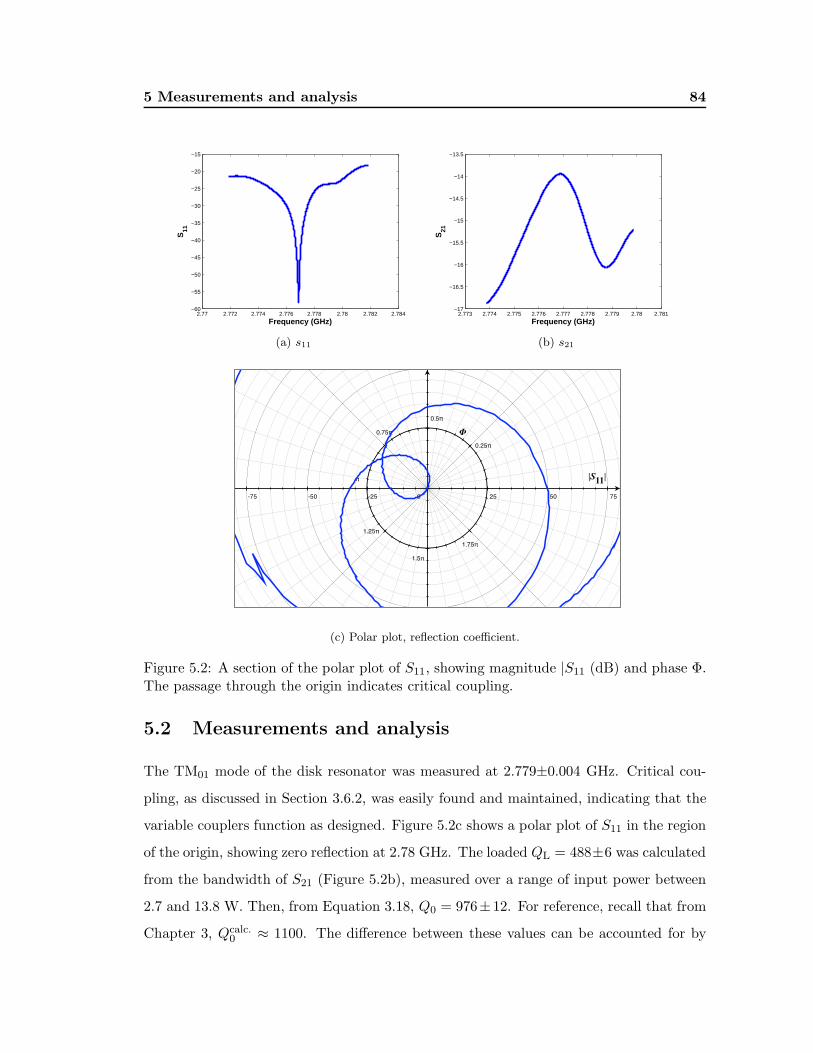
5 Measurements and analysis 84
2.77 2.772 2.774 2.776 2.778 2.78 2.782 2.784−60
−55
−50
−45
−40
−35
−30
−25
−20
−15
Frequency (GHz)
S11
(a) s11
2.773 2.774 2.775 2.776 2.777 2.778 2.779 2.78 2.781−17
−16.5
−16
−15.5
−15
−14.5
−14
−13.5
Frequency (GHz)
S21
(b) s21
-75 -50 -25 0 25 50 75
0.25π
0.5π
0.75π
π
1.25π
1.5π
1.75π
|S11|
Φ
(c) Polar plot, reflection coefficient.
Figure 5.2: A section of the polar plot of S11, showing magnitude |S11 (dB) and phase Φ.The passage through the origin indicates critical coupling.
5.2 Measurements and analysis
The TM01 mode of the disk resonator was measured at 2.779±0.004 GHz. Critical cou-
pling, as discussed in Section 3.6.2, was easily found and maintained, indicating that the
variable couplers function as designed. Figure 5.2c shows a polar plot of S11 in the region
of the origin, showing zero reflection at 2.78 GHz. The loaded QL = 488±6 was calculated
from the bandwidth of S21 (Figure 5.2b), measured over a range of input power between
2.7 and 13.8 W. Then, from Equation 3.18, Q0 = 976±12. For reference, recall that from
Chapter 3, Qcalc.0 ≈ 1100. The difference between these values can be accounted for by

5 Conclusions 85
losses inherent in the RF measurement circuit, including the 141-R transmission lines.
The multilayer sample shows no resonance for a 100 MHz range about the central
frequency. The only difference between this sample and the control is the presence of
two thin films: (Nb,Ti)N and Al2O3. Large RF surface losses in the thin film layers may
explain why no resonance was observed during multilayer testing. Since the (Nb,Ti)N
deposition process is still being refined, there is a good opportunity here to test films of
different qualities under RF conditions. It’s possible that the (Nb,TiN)N films currently
being made are simply too lossy for RF applications. This question will be resolved via
a further evaluation of the RF surface resistance of sputtered (Nb,Ti)N films, as well as
equivalent measurements made with other materials.
5.3 Conclusions
An experimental program has been developed to evaluate the efficacy of multilayer thin
film coatings for SRF. A disk resonator was simulated, built, and tested. Supporting
systems were also designed and built: a dewar insert to hold and tune the resonator, and
to supply RF power during cryogenic tests; and a sample holder to heat and stabilize
substrates during UHV deposition. In addition, the production of thin (Nb,Ti)N films in
JLab’s UHV system was evaluated and improved.
The system works as designed. That is, the resonator operates at the design frequency.
Notably, the variable couplers are effective in finding and maintaining a state of critical
coupling throughout RF measurements. Q0 is also close to predicted values.
A comprehensive evaluation of multilayer films will require several more years of ex-
perimentation. Films of different materials, with varying thickness and surface roughness,
should be tested. This dissertation demonstrates, though, that the system functions and
can be used for such a long-term program.
5.4 Future work
Ultimately, a complete multilayer film evaluation should be conducted in such a way
that samples can be coated with films and then measured quickly and easily. The main
improvement to be made, then, is procedural. The relatively new Thin Film Group

5 Future work 86
at Jefferson Lab will begin using the disk resonator for multilayer analysis. From an
administrative standpoint, the analysis will be incorporated into the broader goals of
Jefferson Lab. This means improved access to lab resources, such as a regular place in
the VTA schedule.
Apart from administrative improvements, the film deposition process must be refined.
Largely, this means completing the commissioning of the UHV system. Mass flow control
will be installed, for example. From the perspective of an extended analysis of multilayer
films, one significant improvement would be to reconfigure the chamber interior. A center-
mount setup would allow several substrates to be coated simultaneously, speeding up
sample production and eliminating chamber environment variations between samples. A
turntable configuration would allow the magnetrons to be mounted on the chamber walls,
freeing up functional space in the chamber and allowing precise masking and patterning
of the samples.
Some modifications can be made to the apparatus itself. For example, Figure 3.15
indicates that the TWTA provides insufficient power to quench bulk Nb. Procuring a
higher-gain S-band TWTA would solve this problem, but radiative losses could also be
reduced by replacing the input coupler with a coaxial probe [133,134]. Furthermore, the
141-R line used to transmit power through liquid helium to the disk resonator is quite
lossy, which makes coupling more difficult. Semirigid, small-diameter heliax line may be
a better alternative.
The frequency of the disk resonator is not fixed. That is, testing samples at other
frequencies in principle requires only the fabrication of a new disk with a different radius.
A disk with an 8 cm diameter could make multilayer measurements at CEBAF’s 1.5 GHz,
for a more direct evaluation of materials for elliptical cavity applications. Or, a higher
frequency could be used to accommodate smaller samples, with the aim of improved
control over film uniformity. The only limitation here is the availability of RF amplifiers
and other hardware that function at the required frequency.
The UHV system is not the only system capable of producing multilayer coatings. The
Thin Film Group at Jefferson Lab is currently exploring methods of energetic deposition
via plasma and electron-cyclotron resonance. At Argonne National Lab, atomic layer film

5 Future work 87
deposition has been generating a fair amount of excitement in the SRF community [116].
And other labs are developing new and promising materials like MgB2 [59]. Since the
disk resonator system only requires flat samples, multilayer substrates do not have to be
prepared in-house.
Finally, the disk resonator system has other applications besides an evaluation of
multilayer films. The RF surface resistance of various materials can be measured over
a broad range of frequencies and temperatures. In addition, there is some debate about
the influence of grain boundary density during vortex penetration [132]. To study this
phenomenon, Q vs. H curves could be measured for bulk niobium substrates with a broad
range of grain boundary densities and surface treatments.

Appendix A
Field solutions in a pillbox cavity
A derivation is presented here of the analytic field solutions in a pillbox cavity. This is
an extension of the material in Section 1.2.1.
As stated above, the starting point is a differential equation obtained from Maxwell’s
equations.
∇× E = − ıωµH (A.1a)
∇×H = ıωǫE + J (A.1b)
∇ ·D = ρ (A.1c)
∇ · B = 0. (A.1d)
Within the volume of the cavity J = 0, simplifying Equation A.1b. Solving for H in
Equation A.1a and substituting gives
∇×∇× E = ω2ǫµE. (A.2)
The left-hand side of Equation A.2 is simplified by using the vector identity ∇×∇×A =
∇(∇ · A) −∇2A and Equation A.1c, which gives ∇ ·E = 0. Then
∇2E + ǫµω2E = 0.
In cylindrical coordinates (r, φ, z),
1
ρ
∂Ez
∂ρ
(
ρ∂Ez
∂ρ
)
+1
ρ2
∂2Ez
∂φ2+
∂2Ez
∂z2+ ω2µǫEz = 0. (A.3)

89
A solution to Equation A.3 is obtained using the separation of variables approach.
Assuming that each of the coordinate dependencies of Ez can be factored,
Ez(ρ, φ, z) = R(ρ)P (φ)Z(z).
The boundary conditions at z = 0, L require Z(z) = sin(βz). Substituting the above form
into Equation A.3, multiplying by ρ2, and dividing by RPZ gives
ρ
R
∂
∂ρ
(
ρ∂R
∂ρ
)
+1
P
∂2P
∂φ2+ ρ2(ω2µǫ − β2) = 0.
Both of these terms are then independent of the other and can therefore each be expressed
as a separation constant. That is,
1
P
∂2P
∂φ2≡ n2
which can be solved by inspection:
P (φ) = E′
0 cos(nφ). (A.4)
(An arbitrary choice of phase, φ → φ + φ0, allows Equation A.4 to be expressed in
simplified form, rather than as a linear combination of sines and cosines. The associated
coefficient is rolled into E0.)
R(ρ) is similarly solved.
ρ
R
∂
∂ρ
(
ρ∂R
∂ρ
)
− n2 + ρ2(ω2µǫ − β2) = 0.
This is Bessel’s equation and the solution is a linear combination of Bessel functions,
R(ρ) = AJn(kcρ) + BYn(kcρ). A cutoff wavenumber is defined, k2c ≡ ω2µǫ − β2. The
cutoff wavenumber is so called because for small values of ω, the argument kcρ becomes
imaginary1. In physical terms, the cavity fields are evanescent and propagation gives way
to attenuation. Finally, note that Yn(kcρ) is singular at ρ → 0. Physical solutions then
require B = 0. The full field solution is therefore
Ez(ρ, φ, z) = E0Jn(kcρ) cos(nφ) sin(βz). (A.5)
1In fact, the “cutoff frequency” is a more widely-used term.
90
The boundary condition Ez(z = L) = 0 constrains the possible values of β such that
sin(βℓ) = 0, or β = pπ/ℓ where p is an integer. Similarly, kc is constrained at the outer
radius R of the cavity.
Ez(ρ = R) = 0 ⇒ Jn(kcR) = 0
so kcR must equal xmn, the set of zeroes to the Bessel function Jn.
k2c = k2 − β2
x2nm
R2= ω2µǫ − p2π2
ℓ2
or, solving for the resonant frequency f = ω/2π,
fnmp =c
2π√
µǫr
√
(xmn
R
)2
+(pπ
ℓ
)2
. (A.6)
Implicit in the above statement is the relation between c and the dielectric constant ǫr.
That is, c = 1/√
µǫ0ǫr. The cavity material here is assumed to be nonmagnetic, such that
µ = µ0.
The indices (n,m, p) give the various eigenfrequencies of the cavity fields. The funda-
mental, accelerating mode is denoted TM010. Since n = p = 0 and β = 0 for this mode,
Equation A.6 simplifies to
f010 =c
2π√
ǫr
∣
∣
∣
xnm
R
∣
∣
∣.
For ℓ = 10 cm and ǫr = 1 (i.e. vacuum), f010 = 1.1 GHz. The magnetic field corresponding
to Equation A.5 is found directly using Maxwell’s equations, specifically Equation A.1a.
For the TM010 mode,
H(TM010) = − ıE0
ηJ1(kρ)φ (A.7)
where η =√
µ/ǫ = 377 Ω is the wave impedance of free space.

Bibliography
[1] A. Gurevich, Applied Physics Letters 88, 1 (2006).
[2] J. Cockcroft and E. Walton, Proc. of the Royal Society A 129, 477 (1930).
[3] J. Cockcroft and E. Walton, Proc. of the Royal Society A 137, 229 (1932).
[4] R. Van de Graaff, K. Compton, and L. Van Atta, Phys. Rev. 43, 149 (1933).
[5] L. Van Atta, D. Northrup, C. Van Atta, and R. Van de Graaff, Phys. Rev.
49, 761 (1936).
[6] T. Aitken, Nuclear Instruments and Methods in Physics Research A 338, 10
(1993).
[7] G. Alton and J. Beene, J. Phys. G: Nucl. Part. Phys. 24, 1347 (1998).
[8] G. Norton and J. Duggan, in Handbook of accelerator physics and engineering,
3rd ed., edited by A. Chao and M. Tigner (World Scientific Publishing Co.
Pte. Ltd., Hackensack, NJ, 2006), Chap. 1.6.10, p. 30.
[9] E. Lawrence and M. Livingston, Phys. Rev. 40, 19 (1930).
[10] A. Grinberg, Sov. Phys. Usp. 18, 815 (1975).
[11] R. Wideroe, in The Infancy of Particle Accelerators: Life and Work of Rolf
Wideroe, edited by P. Waloschek (Friedr. Vieweg Verlagsgesellschaft, London,
UK, 1994), No. DESY-Red-Report 94-039.
[12] D. Sloan and E. Lawrence, Phys. Rev. 38, 2021 (1931).

BIBLIOGRAPHY 92
[13] L. Brillouin, Phys. Rev. 74, 90 (1948).
[14] L. Brillouin, J. Phys. Radium 1, 377 (1930).
[15] L. Brillouin, Proc. of the National Academy of Sciences 41, 401 (1955).
[16] S. Lee, Accelerator Physics, 2nd ed. (World Scientific Publishing Co. Pte. Ltd.,
Hackensack, NJ, 2004).
[17] P. Farnsworth, Multipactor phase control, U.S. Patent 2,071,517, 1935.
[18] W. Gallagher, in Proc. of the 1989 Particle Accelerator Conference, IEEE (,
Chicago, IL, USA, 1989), pp. 2008–2009.
[19] P. Kneisel, O. Stoltz, and J. Halbritter, J. Appl. Phys. 44, 1785 (1973).
[20] J. Halbritter, in Proc. 1st Workshop on RF Superconductivity, edited by
M. Kuntze (Kernforschungszentrum Karlsruhe, Karlsruhe, Germany, 1980),
No. KfK-3019, pp. 190–214.
[21] H. Padamsee and A. Joshi, J. Appl. Phys. 50, 1112 (1979).
[22] H. Piel, in Proc. 1st Workshop on RF Superconductivity (Kernforschungszen-
trum Karlsruhe, Karlsruhe, Germany, 1980), No. KfK-3019, pp. 85–118.
[23] P. Kneisel, IEEE Transactions on Applied Superconductivity 9, 1023 (1999).
[24] R. Sundelin, IEEE Transactions on Nuclear Science NS-32, 3570 (1985).
[25] H. A. Grunder et al., Nuclear Physics A 478, 831 (1988).
[26] H. Padamsee and et al., in Proc. of the 1991 Particle Accelerator Conference
(IEEE, San Francisco, CA, 1991), pp. 786–788.
[27] G. Ciovati and et al., in Proc. 10th Workshop on RF Superconductivity (,
Tsukuba, Japan, 2001), No. PT016, pp. 512–516.
[28] W. Weingarten, in Proc. 7th Workshop on RF Superconductivity, CERN (,
Gif-sur-Yvette, France, 1995), No. CERN-SL-95-122 RF, pp. 23–26.

BIBLIOGRAPHY 93
[29] R. Geng, G. Eremeev, H. Padamsee, and V. Shemelin, in Proceedings of
PAC07, IEEE (, Albuquerque, New Mexico, USA, 2007), No. WEPMS006,
pp. 2337–2339.
[30] H. Hayano, in Proceedings of 2005 Particle Accelerator Conference (IEEE,
Knoxville, TN, 2005), No. WOAA002.
[31] ITRP, Technical report, ILC (unpublished).
[32] J. Wang et al., in Proceedings of the 1995 Particle Accelerator Conference
(IEEE, Dallas, Texas, USA, 1995), Vol. 1, pp. 653–655.
[33] E. Vogt, IEEE Transactions on Nuclear Science NS-30, 3684 (1983).
[34] J. Calarco et al., IEEE Transactions on Nuclear Science NS-24, 1091 (1977).
[35] J. Halbritter, Z. Physik 266, 209 (1974).
[36] H. Padamsee, J. Knobloch, and T. Hays, RF Superconductivity for Accelera-
tors, 2nd ed. (Wiley-VCH Verlag GmbH & Co. KGaA, Weinheim, Germany,
2008).
[37] D. Boussard and T. Linnecar, in Proceedings of the 1999 Cryogenic Engineer-
ing and International Cryogenic Materials Conference (CE-ICM, Montreal,
Canada, 1999), No. LHC-PR-316.
[38] M. Tinkham, Introduction to Superconductivity, 2nd ed. (Dover Publications,
Inc., Mineola, NY, USA, 1996).
[39] A. Leggett, Quantum Liquids: Bose condensation and Cooper pairing in
condensed-matter systems (Oxford University Press, Oxford, England, 2006).
[40] A. Abrikosov, L. Gorkov, and I. Dzyaloshinski, in Methods of Quantum Field
Theory in Statistical Physics, 2nd ed., edited by R. A. Silverman (Prentice-
Hall, Inc., Edgewood Cliffs, NJ, USA, 1963).
[41] C. Kittel, Quantum Theory of Solids, 2nd ed. (J. Wiley & Sons, Inc., New
York, NY, 1963).

BIBLIOGRAPHY 94
[42] F. London and H. London, in Proceedings of the Royal Society of London,
No. 866 in A: Mathematical and Physical Sciences (The Royal Society, London,
UK, 1935), pp. 71–88.
[43] R. Cohen and B. Abeles, Phys. Rev. 168, 167 (1968).
[44] K. Kanoda et al., Phys. Rev. Lett. 65, 1271 (1990).
[45] J. Bardeen, L. Cooper, and J. Scrieffer, Physical Review 108, 1175 (1957).
[46] K. Saito, in Proceedings of the 2003 Particle Accelerator Conference, IEEE (,
Portland, OR, USA, 2003), pp. 462–466.
[47] T. Yogi, G. Dick, and J. Mercereau, Phys. Rev. Lett. 39, 826 (1977).
[48] D. Proch, Reports on Progress in Physics 61, 431 (1998).
[49] A. Valente-Feliciano, in Proc. 13th Workshop on RF Superconductivity (Bei-
jing University, Beijing, China, 2007).
[50] S. Deambrosis et al., in Proceedings of the 14th International Conference
on RF Superconductivity (pending publication, Berlin, Germany, 2009),
No. TUOBAU07.
[51] C. Leemann, D. Doublas, and G. Krafft, Annu. Rev. Nucl. Part. Sci. 51, 413
(2001).
[52] P. Kneisel, G. Myneni, and G. Ciovati, in Proceedings of 2005 Particle Accel-
erator Conference (IEEE, Knoxville, TN, 2005), No. TPPT076.
[53] R. Geng, H. Padamsee, A. Seaman, and V. Shemelin, in Proceedings of 2005
Particle Accelerator Conference, PAC (, Knoxville, TN, 2005), No. ROAC009.
[54] G. Wu, L. Cooley, C. Antoine, and H. Edwards, in Proceedings of SRF2007,
SRF (Peking University, Beijing, China, 2007), No. TU204.
[55] P. Bauer et al., in Proc. 12th International Workshop on RF Superconductivity
(, Ithaca, NY, 2005).

BIBLIOGRAPHY 95
[56] H. Wang et al., in Proceedings of 2005 Particle Accelerator Conference, PAC
(IEEE, Knoxville, TN, 2005), No. TPPT085.
[57] P. Fabbricatore and et al., IEEE Transactions on Applied Superconductivity
3, 1761 (1993).
[58] A. Rossi et al., in Proceedings of the 14th International Conference
on RF Superconductivity (pending publication, Berlin, Germany, 2009),
No. TUOBAU06.
[59] T. Tajima and et al., in Proceedings of the 2006 Applied Superconductivity
Conference (IEEE, Seattle, WA, USA, 2006), No. LA-UR-06-6143.
[60] C. Wyss, in Record of the 1991 IEEE Particle Accelerator Conference (IEEE,
San Francisco, CA, USA, 1991), pp. 150–152 vol. 1.
[61] R. Di Leo, A. Nigro, G. Nobile, and R. Vaglio, Journal of Low-Temperature
Physics 78, 41 (1990).
[62] G. Stejic et al., Phys. Rev. B 49, 1274 (1994).
[63] M. Marino, in Proc. 8th Workshop on RF Superconductivity, CERN (, Abano-
Terme, Italy, 1997), Vol. 1-4, pp. 1074–1080.
[64] S. Bedorf, Ph.D. thesis, University of Koln, Koln, Germany, 2005.
[65] A. Gurevich and R. Mints, Rev. Mod. Phys. 59, 941 (1987).
[66] Z. Zhang and M. Lagally, Science 276, 377 (1997).
[67] I. Petrov and et al., J. Vac. Sci. Technol. A 21, S117 (2003).
[68] B. Josephson, Rev. Mod. Phys. 36, 216 (1964).
[69] N. Lutke-Entrup, B. Placais, P. Mathieu, and Y. Simon, Phys. Rev. Lett. 79,
2538 (1997).
[70] D. Vodolazov, I. Maksimov, and E. Brandt, Physica C 384, 211 (2003).

BIBLIOGRAPHY 96
[71] C. Antoine and et al., in Proceedings of the 14th International Conference on
RF Superconductivity (SRF, Berlin, Germany, 2009), No. TUPPO070.
[72] R. Russo and et al., IEEE Transactions on Applied Superconductivity 19,
1394 (2009).
[73] L. Lilje, in Proc. Linear Accelerator Conference (, Lubeck, Germany, 2004),
No. WE102.
[74] G. Ciovati et al., Physical Review Special Topics - Accelerators and Beams
13, 1 (2010).
[75] C. Reece and et al., in Proceedings of 2005 Particle Accelerator Conference,
IEEE (, Knoxville, TN, 2005), pp. 4081–4083.
[76] K. Saito and et al., in Proc. 14th International Conference on RF Supercon-
ductivity (, Berlin, Germany, 2009), No. THOAAU05, pp. 467–472.
[77] G. Ciovati et al., in Proc. 13th International Workshop on RF Superconduc-
tivity (, Beijing, China, 2007).
[78] A. Derneryd, IEEE Transactions on Antennas and Propagation AP-27, 660
(1979).
[79] A. Jenkins et al., IEEE Transactions on Applied Superconductivity 7, 2793
(1997).
[80] I. Wolff and N. Knoppik, IEEE Transactions on Microwave Theory and Tech-
niques MTT-22, 857 (1974).
[81] C. Grebenkemper and J. Hagen, Phys. Rev. 80, 89 (1950).
[82] N. M. Alford and et al., Journal of the European Ceramic Society 21, 2605
(2001).
[83] A. Bhattacharyya and R. Garg, IEEE Transactions on Antennas and Propa-
gation AP-33, 1067 (1985).

BIBLIOGRAPHY 97
[84] T. Itoh and W. Menzel, IEEE Transactions on Antennas and Propagation
AP-29, 63 (1981).
[85] J. James and G. Wilson, Microwaves, Optics and Acoustics 1, 165 (1977).
[86] W. Harokopus and et al., IEEE Transactions on Microwave Theory and Tech-
niques 39, 1098 (1991).
[87] M. Bartsch and et al., Computer Physics Communications 72, 22 (1992).
[88] T. Weiland, International Journal of Numerical Modeling: Electronic Net-
works, Devices and Fields 9, 295 (1996).
[89] A. Andreone and et al., J. Appl. Phys. 73, 4500 (1993).
[90] C. Benvenuti, P. Chiggiato, L. Parrini, and R. Russo, Nuclear Instruments
and Methods in Physics Research B 124, 106 (1997).
[91] N. Iosad and et al., IEEE Transactions on Applied Superconductivity 11, 3832
(2001).
[92] H. Myoren and et al., IEEE Transactions on Applied Superconductivity 11,
3828 (2001).
[93] C. Reece, J. Susta, T. Powers, and B. Almeida, in Proceedings of the 1991
Particle Accelerator Conference (IEEE, San Francisco, CA, USA, 1991), pp.
2325–2327.
[94] R. Barron, in Cryogenic Systems, 2nd ed., edited by R. Scurlock (Oxford
University Press, New York, NY, 1985).
[95] S. Cantacuzene et al., in Proceedings of European Particle Accelerator Con-
ference (, Lucerne, Switzerland, 1994), pp. 2074–2076.
[96] B. Jackson and et al., J. Appl. Phys. 97, 1 (2005).
[97] C. Tong and et al., in Proc. 12th International Symposium on Space Terahertz
Technology, edited by I. Mehdi (, Pasadena, CA, 2001), pp. 253–261.

BIBLIOGRAPHY 98
[98] S. Boelens and H. Veltrop, Surface and Coatings Technology 33, 63 (1987).
[99] U. Konig, Surface and Coatings Technology 33, 91 (1987).
[100] Handbook of Ternary Alloy Phase Diagrams, edited by P. Villars, A. Prince,
and H. Okamoto (ASM International, Materials Park, OH, USA, 1995),
Vol. 10.
[101] V. Buscaglia and et al., Journal of Alloys and Compounds 226, 232 (1995).
[102] E. Felten, Journal of the Less-Common Metals 17, 207 (1969).
[103] V. Buscaglia and et al., Journal of Alloys and Compounds 283, 241 (1999).
[104] C. Yen and et al., J. Appl. Phys. 38, 2268 (1967).
[105] E. Cukauskas, W. Carter, and S. Qadri, J. Appl. Phys. 57, 2538 (1985).
[106] Z. Wang and et al., J. Appl. Phys. 79, 7837 (1996).
[107] V. Zhitomirsky and et al., Thin Solid Films 326, 134 (1998).
[108] Binary Alloy Phase Diagrams, 2nd ed., edited by T. Massalski, H. Okamoto, P.
Subramanian, and L. Kacprzak (ASM International, Metals Park, OH, USA,
1990), Vol. 3.
[109] R. Reed-Hill and R. Abbaschian, Physical Metallurgy Principles, 3rd ed.
(PWS-Kent Pub., Boston, MA, USA, 1992).
[110] in Powder Diffraction File, edited by S. Kabekkodu (International Centre for
Diffraction Data, Newton Square, PA, USA, 2011).
[111] E. Cukauskas, J. Appl. Phys. 54, 1013 (1983).
[112] A.-M. Valente-Feliciano et al., in Proceedings of the 14th International Con-
ference on RF Superconductivity (, Berlin, Germany, 2009), No. TUPPO084.
[113] M. Voigt and M. Sokolowski, Materials Science and Engineering B 109, 99
(2004).

BIBLIOGRAPHY 99
[114] M. Voigt and et al., J. Vac. Sci. Technol. A 27, 234 (2009).
[115] B. Segda, M. Jacquet, and J. Besse, Vacuum 62, 27 (2001).
[116] T. Proslier and et al., Applied Physics Letters 93, 1 (2008).
[117] B. Argent and B. Phelps, Journal of the Less-Common Metals 2, 181 (1960).
[118] G. Jouve, C. Severac, and S. Cantacuzene, Thin Solid Films 287, 146 (1996).
[119] G. Wu, Ph.D. thesis, Virginia Polytechnic Institute, Blacksburg, VA, USA,
2002.
[120] T. Matsunaga, H. Maezawa, and T. Noguchi, IEEE Transactions on Applied
Superconductivity 13, 3284 (2003).
[121] P. Bosland, F. Guemas, and M. Juillard, in Proceedings of European Particle
Accelerator Conference (, Paris, France, 1992), pp. 1316–1318.
[122] I. Safi, Surface and Coatings Technology 127, 203 (2000).
[123] L.-J. Meng and M. dos Santos, Surface and Coatings Technology 90, 64 (1997).
[124] J. Thornton, J. Vac. Sci. Technol. A 4, 3059 (1986).
[125] Z.-J. Liu and et al., J. Appl. Phys. 92, 3559 (2002).
[126] J. Goldstein and et al., Scanning electron microscopy and x-ray microanalysis,
3rd ed. (Springer Science + Business Media, Inc., New York, NY, 2003).
[127] B. Cullity and S. Stock, Elements of x-ray diffraction, 3rd ed. (Prentice-Hall,
Inc., New York, NY, 2001).
[128] M. Torche and et al., Thin Solid Films 436, 208 (2003).
[129] J. Sundgren, Thin Solid Films 128, 21 (1985).
[130] A. Denton and N. Ashcroft, Physical Review A 43, 3161 (1991).
[131] A. Patterson, Phys. Rev. 56, 978 (1939).

BIBLIOGRAPHY 100
[132] P. Lee and et al., Physica C 441, 126 (2006).
[133] A. Tulintseff and S. Ali, IEEE Transactions on Antennas and Propagation 39,
381 (1991).
[134] M. Davidovitz and Y. Lo, IEEE Transactions on Antennas and Propagation
AP-34, 905 (1986).