A.-M. Valente-Feliciano SRF Materials Workshop-May 24, 2007 Overview New Materials for SRF Cavities...
41
A.-M. Valente-Feliciano SRF Materials Workshop-May 24, 2007 Overview Overview New Materials for SRF New Materials for SRF Cavities Cavities Anne-Marie Valente-Feliciano Jefferson Lab/JSA
-
Upload
brian-patterson -
Category
Documents
-
view
216 -
download
1
Transcript of A.-M. Valente-Feliciano SRF Materials Workshop-May 24, 2007 Overview New Materials for SRF Cavities...

A.-M. Valente-FelicianoSRF Materials Workshop-May 24, 2007
OverviewOverview
New Materials for SRF New Materials for SRF CavitiesCavities
Anne-Marie Valente-FelicianoJefferson Lab/JSA

A.-M. Valente-FelicianoSRF Materials Workshop-May 24, 2007
•Motivation
•Which Superconductors for SRF Cavities?
•Nb compoundsNbNNbTiN
•A15 Compounds:Nb3SnV3Si
•MgB2
•SIS Multilayer Structures
•Concluding Remarks
OutlineOutline

A.-M. Valente-FelicianoSRF Materials Workshop-May 24, 2007
Nb has the highest Tc for a pure metal and the highest lower magnetic field Hc1
•Nb cavities performance have reached close to its theoretical limit (H Hc = 200 mT)
•For further improved cavity RF performance, innovation needed
•Higher Tc , potentially higher Hc
•Substrates with higher thermal conductivity
•Potentially cryogenics cost reduction if cavity operation temperature at 4.2K or higher
Why looking beyond Nb?Why looking beyond Nb?
KEK&Cornell

A.-M. Valente-FelicianoSRF Materials Workshop-May 24, 2007
The power dissipated per unit area of SC in RF regime
and If T < Tc / 2
Which superconductors are suitable for SRF applications? Which superconductors are suitable for SRF applications?
2
2HRP S resBCSS RTRR )(
Empirically, Rres found proportional to at least √n
For low RF losses, a high TC value is not sufficient
A metallic behaviour (low normal resistivity) in the
normal state is mandatory
Residual Resistance RresResidual Resistance Rres
Inhomogeneties, Grain Boundaries, Surface Serration
18Tc (K)
ρn
(μΩ
cm)
RBCS IdealR BCS ~ 1 nΩ~ 10 μΩcm
V. Palmieri, 10th Workshop on RF Superconductivity Proceedings, Tsukuba 2001 (Noguchi) “New materials for superconducting radiofrequency cavities”

A.-M. Valente-FelicianoSRF Materials Workshop-May 24, 2007
Choices among Superconducting MaterialsChoices among Superconducting Materials
Material
Tc (K) ρn(μΩcm)
Hc(0) [T] Hc1(0) [T]
Hc2(0) [T] (0) [nm]
Nb 9.2 2 0.2 0.17 0.4 40
NbN 16.2 70 0.23 0.02 15 200
NbTiN 17.5 35 0.03 151
Nb3Sn 18 20 0.54 0.05 30 85
V3Si 17
Mo3Re 15 0.43 0.03 3.5 140
MgB2 40 0.43 0.03 3.5 140
Nb compounds A15 compounds MgB2

A.-M. Valente-FelicianoSRF Materials Workshop-May 24, 2007
Nb CompoundsNb Compounds
B1 compounds – NaCl structure
Only few Nitrides and Carbides of the IV, V and VI group Transition Metals have critical temperatures higher than Niobium.

A.-M. Valente-FelicianoSRF Materials Workshop-May 24, 2007
Nb Compounds - NbNNb Compounds - NbN
The only B1 simple compound that has widely tested for accelerating cavities
Mainly two different techniques have been investigated:
•Thermal diffusion of N into Nb followed by rapid quench cooling •Reactive Sputtering on metallic or ceramic substrates to Nb cavitiesThermal Diffusion:
Bulk Nb (RRR 300) annealed @ 1550˚C for 2h +
reacted in N2 vapor(150mbar) @ 1400˚C for 4hRs=1.3 10-6 @ 4.2K and 4 10-9 @1.8K @7.9GHz
G.Gemme et al., J.Appl.Phys. 77(1), Jan. 1995Reactive Sputtering:
Sputtering from high purity Nb target in Ar + N2 in DC triode magnetron sputtering system
Highest Tc for substrate temp. > 500˚C, PAr=8.10-3mbar, PN2=1.10-3mbar
A. Nigro et al., Physica Scripta Vol. 38, 483-485, 1988

A.-M. Valente-FelicianoSRF Materials Workshop-May 24, 2007
Nb Compounds - NbNNb Compounds - NbN
Good SC properties, even if deposited at low temperatureLow secondary emission coefficient
Very stable surface properties
Tc= 17.2 K for δ-phase (lattice parameter = 4.388 Å) TC very sensitive to Nitrogen stoichiometry
. In sputtered films, the δ -phase can be found mixed to some other low TC phases
Even if no grain boundaries are present and δ-phase single crystal is considered the single grain resistivity is not so low.
Anomalously high resistivity of NbN in the normal state, often higher than 100 μΩcm due to both metallic and gaseous vacancies randomly distributed
in both sublattices Equiatomic composition is Nb0.987N0.987 not Nb1.0N1.0
Common problem for B1 compounds

A.-M. Valente-FelicianoSRF Materials Workshop-May 24, 2007
Nb Compounds - NbTiNNb Compounds - NbTiN
INFN : reactive sputtering with Ar/N2 in DC Triode Magnetron Sputtering @ 600˚C and 200˚C
(Nb~ xTix )N films with x ~< 0.5 present a lower calculated surface impedance than NbN, especially when deposited at low temperatures.
R. Di Leo et al. J. of Low Temp. Phys, vol 78, n1/2, pp41-50, 1990
extreme hardness, excellent adherence on various substrates, very good corrosion and erosion resistance, high-sublimation temperature, and relative inertness
More metallic nature and better surface properties than NbN should result in better rf performances

A.-M. Valente-FelicianoSRF Materials Workshop-May 24, 2007
Nb Compounds - NbTiNNb Compounds - NbTiNReactive Magnetron Sputtering:
CEA Saclay : NbTiN films deposited on 12 cm copper disks by magnetron sputtering and tested in a cylindrical TEOll cavityreached RF field levels of 35 mT low residual surface resistance (< 100 nΩ at 4 GHz) with a very small BCS resistance4 cavities deposited but no RF measurement due to film blistering on large area of the cavity.Rs slope significantly decreased when coating with bias ranging from -50V to -100V
P. Bosland et al.S. Cantacuzène et al.
CERN:Samples and six 1.5 GHz Cu cavities coated by reactive cylindrical magnetron sputteringBest cavity result for thicker film (4.3μm) and lower deposition temperature ( 265˚C)Rs = 330nΩ @ 4.2KQ0 at zero field is higher than the Q-value of Niobium cavities but Eacc limited under 10 MV/mAs for NbN, N stoichiometry critical to obtain the right SC phase
M. Marino, Proceedings of the 8th Workshop on RF Superconductivity, October 1997, Abano Terme (Padua), (Rep) 133/98, vol.IV, p.1076

A.-M. Valente-FelicianoSRF Materials Workshop-May 24, 2007
A15 Compounds
• Among the Nb and V based high Tc (15 – 20 K)
• Nb3Ga and Nb3Ge do not exist as stable bulk materials at 3:1 stoichiometry
• Nb3Al exists only at high temperature causing excessive atomic disorder • Production of above materials need non equilibrium processes
• V3Ga, V3Si & Nb3Sn are stable bulk material and have high Tc
• Yet another A-15 compound holding promise is Mo3Re (Tc=15K)
Choice of A-15 Compounds for RF Cavities
Structure
B atoms occupy corners and centre of BCC structureA atoms form orthogonal chains bisecting the faces of the BCC unit cell. Linear Chain Integrity is crucial for Tc

A.-M. Valente-FelicianoSRF Materials Workshop-May 24, 2007
A15 Compounds – Preparation MethodsExtreme brittleness so A-15 bulk structure cannot be formed
The A-15 should be produced as thin layer on the interior of the already formed structure
Such a layer need to be only a micron or two thick λL (Nb3Sn) = 65 nm
Thin film route idealCo-Sputtering
• Considerable success achieved in synthesizing difficult materials like Nb3Ge with highest Tc(~23k) or V3Si
• Typically two constituents are sputtered simultaneously onto a temperature controlled substrate
• Stoichiometry dependent on relative positions of target and substrate (can be manipulated to get perfect stoichiometry)
• Stoichiometry control difficult over large areas like accelerating system and if stoichiometry range for A-15 phase is narrow.
Sputtering To sputter from a single target of correct stoichiometry (prepared by powder sintering)
Stoichiometry, Substrate Temperature, Deposition Rate, Deposition Thickness Can be varied independently
Chemical Vapor Deposition (CVD)
MOCVD (Metal Organic Chemical Vapour Deposition) is a particular case of CVD in which the precursor is a metallorganic compound
Process in which one or more precursors, present in vapor phase, chemically react on an appropriate warm substrate, giving rise to a solid film
Deposition rate and structure of the film depend upon temperature and reagent concentration Uniformity of temperature and flow of gaseous over entire cavity surface may be
difficult with complex geometry
Diffusion Reaction
Technique proved successful for magnet conductor applicationSimple equipment compared to sputtering and CVD
A.-M. Valente-FelicianoSRF Materials Workshop-May 24, 2007
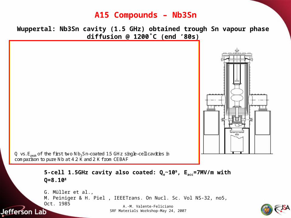
A15 Compounds – Nb3Sn
Q vs. Epeak of the first two Nb3Sn-coated 1.5 GHz single-cell cavities in comparison to pure Nb at 4.2 K and 2 K f romCEBAF
Wuppertal: Nb3Sn cavity (1.5 GHz) obtained trough Sn vapour phase diffusion @ 1200˚C (end ’80s)
5-cell 1.5GHz cavity also coated: Qo~109, Eacc=7MV/m with Q=8.108
G. Müller et al., M. Peiniger & H. Piel , IEEETrans. On Nucl. Sc. Vol NS-32, no5, Oct. 1985

A.-M. Valente-FelicianoSRF Materials Workshop-May 24, 2007
A15 Compounds – Nb3Sn
Nb3Sn coatings on Nb by liquid diffusion method at INFN Legnaro“Hybrid” Process”
•Substrate thermalization (30 min - 1 h)•Dipping (few min - 2 h)•Sample annealing with Sn vapor for a few hours•Sample annealing without Sn vapor for a few hours
Linearfeedtrough
Cooling water jacket
Furnace
Liquid Sn
Furnace
-0,028
-0,026
-0,024
-0,022
-0,02
-0,018
-0,016
-0,014
-0,012
1 3 5 7 9 11 13 15 17 19
Temperature (K)
M' (
emu)
Proc T = 975°C, Dipp t = 30’, Ann (Sn) t = 2h, Ann t = 5h
Good Nb3Sn film superconductive properties
No Residual Sn traces on the sample surface
Tc = 16,5 K, DTc = 0,3 K
No Sn rich Phases
Diffusion temperature to be kept above 9300C to avoid formation of low Tc phases like Nb6Sn5 ( 2.6 K ) and NbSn2 ( 2.1 K )Diffusion time optimize to obtain desired Nb3Sn thicknessPost diffusion heat reaction important to get rid of the outer Sn layerPost diffusion annealing to have enlarged grains and perfect ordering
S. Deambrosis, Sharma, LNL-INFNInternational SRF Thin Films Workshop, 2006

A.-M. Valente-FelicianoSRF Materials Workshop-May 24, 2007
Nb3Sn - MOCVD process & otherNb3Sn - MOCVD process & other
Sample characterization by XRD, SEM and RBS analyses: presence of niobium (I, II, V) and tin (II) oxides on the surface.
Nb3Sn Coating through Multilayer Structure (Keppel, LNL/INFN)Coat alternate layers of Nb and Sn and subject to diffusion reaction
Preliminary results: a sharp transition and a Tc of 17 K has been obtained
Problems:great oxophylic character of NbVacuum problem in the systems used
MOCVD technique using bis(cyclopentadienil)niobium borohydride, (cyclopentadienil)niobium tetramethyl and tributyltin hydride as Nb and Sn precursors respectively.
G. Carta et al.

A.-M. Valente-FelicianoSRF Materials Workshop-May 24, 2007
A15 Compounds – Other Materials under DevelopmentA15 Compounds – Other Materials under Development
• Mo3Re thin films by DC magnetron deposition * Sapphire, Cu and Nb substrates used * Substrate temperature up to 9500 C * A Tc = 12K obtained for composition Mo60Re40
• V3Si layers by silanization of V substrate and Thermal Diffusion
V substrate heated to get SiH4 decomposition and Silicon diffusionFilm grown by silanization with p (SiH4) ~ 10-3-10-4 mbarAnnealing in vacuum to get rid of hydrogen
* Diffusion parameters and silane flow rate have been optimized * A Tc = 16 K is routinely obtained * RF measurement on 6 GHz V-cavities will be available soon

A.-M. Valente-FelicianoSRF Materials Workshop-May 24, 2007
Magnesium Diboride (MgBMagnesium Diboride (MgB22) )
C. Buzea and T. Yamashita, Superconductor Sci. Technol. 14 (2001) R115.
Compared to cuprates:
• Cheaper• Lower anisotropy• Larger coherence length• Transparency of grain boundaries to current flows
attractive for RF applications.
Graphite-type boron layers separated by hexagonal close-packed layers of magnesium
Superconductivity comes from the phonon-mediated Cooper pair production similar to the low-temperature superconductors except for the two-gap nature.
A. Floris et al., cond-mat/0408688v1 31 Aug 2004
Nb
RF response has shown lower energy gap behavior.

A.-M. Valente-FelicianoSRF Materials Workshop-May 24, 2007
Hybrid Physical Chemical Vapor Deposition
High Tc has been obtained in polycrystalline MgB2 films on stainless steel, Nb, TiN, and other substrates.
0 50 100 150 200 250 3000.000
0.002
0.004
0.006
0.008
36 37 38 39 40 410.000
0.002
0.004
R ()
T (K)
Re
sist
ance
(O
hm
s)
Temperature (K)
MgB2/Stainless Steel
0 50 100 150 200 250 3000.0
0.5
1.0
1.5
2.0
36 37 38 39 40 410.00
0.05
0.10
0.15
R (
x 1
04
)
T (K)
Res
ista
nce
( x
104
)
Temperature (K)
MgB2/Nb
MgB2 – HPCVD on metal substratesX. Xi- Penn State University
Clean HPCVD MgB2 thin films with excellent properties: •RRR>80low resistivity (<0.1 μΩ) and long mean free path• high Tc ~ 42 K (due to tensile strain), high Jc (10% depairing current)• low surface resistance, short penetration depth• smooth surface (RMS roughness < 10 Å with N2 addition)• good thermal conductivity (free from dendritic magnetic instability)
Critical engineering considerations: generate high Mg pressure at substrate (cold surface is Mg trap)deliver diborane to the substrate (the first hot surface diborane sees should be the substrate)
H2, B2H6
Mg
Susceptor

A.-M. Valente-FelicianoSRF Materials Workshop-May 24, 2007
MgBMgB22 Coating: Reactive Deposition System Coating: Reactive Deposition System
B.H. Moeckly, ONR Superconducting Electronics Program ReviewRed Bank, NJ, February 8, 2005
B.H. Moeckly et al., IEEE Trans. Appl. Supercond. 15 (2005) 3308.T. Tajima et al, Proc. PAC05.
In-situ reactive evaporation @ 550˚C
SuperconductingTechnologies Inc.
Oates, Agassi, and Moeckly, ASC 2006 Proceeding
Compared to Nb: Higher Tc
low resistivitylarger gaphigher critical field
RF measurement @ MIT/Lincoln Lab
T. Tajima, LANL

A.-M. Valente-FelicianoSRF Materials Workshop-May 24, 2007
• MgB2 precursor films formed on Nb (2.5 mm thick) by PLD and annealed at 620oC. • Film partially superconducting.
Pulsed Laser Deposition - S.Mitsunobu et al. , KEK
Low Pressure CVD - L. Crociani,INFN LegnaroInternational Workshop onThin Films and New Ideas for Pushing The Limits Of RF Superconductivity, LNL-INFN , Oct.2006
MgBMgB22 Other production techniques
Challenges
Film properties degrade with exposure to air/moisture: resistance goes up, Tc goes down Clean cavity surface leads to degradation in water and moisture
Safety … procedures for use of diborane
Keys to high quality MgB2 thin films: • High Mg pressure for thermodynamic stability of MgB2• oxygen-free or reducing environment• clean Mg and B sources

A.-M. Valente-FelicianoSRF Materials Workshop-May 24, 2007
SIS MultilayersAlex Gurevich, Appl. Phys. Lett. 88, 012511 (2006)Alex Gurevich, Appl. Phys. Lett. 88, 012511 (2006)
Higher Tc thin layers provide magnetic screening of the bulk SC cavity (Nb, Pb) without vortex penetration
Taking advantage of the high –Tc superconductors without being penalized by their lower Hc1…Multilayer coating of SC cavities: alternating SC and insulating layers with d <
““A minimalistic solution”A minimalistic solution”A Nb cavity coated with an insulator and a single 50 nm thick Nb3Sn layerIf the Nb cavity can withstand Hi = 150mT,then the external field can be as high as 324mT
A single layer coating more than doubles the breakdown field with no vortex penetration, enabling Eacc 100 MV/m
Nb, Pb
Insulating layers
Higher-TcSC: NbN, Nb3Sn, etc
• Strong increase of Hc1 in films allows using rf fields > Hc of Nb, but lower than those at which flux penetration in grain boundaries may become a problem
• Strong reduction of BCS resistance because of using SC layers with higher (Nb3Sn, NbN, etc)

A.-M. Valente-FelicianoSRF Materials Workshop-May 24, 2007
SIS Multilayers: ExperimentsSIS Multilayers: Experiments
• INFN Legnaro
Nb3Sn/Al2O3/Nb (sputtering and thermal diffusion)6GHz cavities coated. RF results soon
• JLab
NbN/Al2O3/Nb and NbTiN/Al2O3/Nb coated in UHV multi-techniques and ECR deposition systems under preparation (combining magnetron sputtering, IBAD, ECR, …)
• Argonne National LabAtomic Layer Deposition (ALD): alternating, saturating reactions between gaseous precursor molecules and a substrate to deposit films layer by layer. Films from a wide variety of elements, compounds and alloys with a thickness from a few atomic monolayers to microns
• Penn State UniversityMgB2 as a top layer with HPCVD

A.-M. Valente-FelicianoSRF Materials Workshop-May 24, 2007
Over the years, some attempts have been made to study alternative materials to Nb for applications to SRF cavities
Most of the sample/cavities using alternative materials have been producedby reactive magnetron sputtering or thermal diffusion. Energetic Condensation Techniques like Vacuum Arc Deposition, ECR, or ALD?
Any material study would ideally combine material, surface analyses with superconducting properties and RF performance…an extensive but necessary mount of work.
The multilayer approach opens the door to further potential improvement for SRF cavities
The effort for new materials research for SRF cavities application has been very limited so far… It took more than 30 years to optimize the cavity performance and come close to the theoretical limit…and a few thousands of men-years…for niobium, a pure metal…
CONCLUDING REMARKS

A.-M. Valente-FelicianoSRF Materials Workshop-May 24, 2007
Larry Phillips, JLabC. Reece, JLabV. Palmieri, S. Deambrosis, LNL-INFNT. Tajima, LANLX. Xi, PSUJ. Elam, ANLA. Gurevich, FSU
Aknowledgements
Thank You !

A.-M. Valente-FelicianoSRF Materials Workshop-May 24, 2007
State-of-the-art at 1500 MHz – 1.7 K – single cellState-of-the-art at 1500 MHz – 1.7 K – single cell
1
10
100
1000
0 5 10 15 20 25
Rs
[nO
hm]
Eacc
[MV/m]
Q 1x10¹⁰ @ 15 MV/m
Q 3x10⁹ @ 20 MV/m
28 MV/m reached in a large LEP cryostat (He evaporation at large power)

A.-M. Valente-FelicianoSRF Materials Workshop-May 24, 2007
LIMITATIONS OF CONVENTIONAL MAGNETRON SPUTTERING FOR LIMITATIONS OF CONVENTIONAL MAGNETRON SPUTTERING FOR THIN FILM SRF CAVITIES THIN FILM SRF CAVITIES
• Microstructure defects and voids
– Caused by lack of condensate mobility, shadowing
– Results in enhanced intergranular oxidation producing “weak links” and associated problems and electronic mean free path limitation
• Small grain size
– Provide an upper limit to the electronic mean free path in the absence of other limiting impurities.
• Sputter gas inclusion in the growing film along with other impurities such as oxygen and hydrogen.
• Film to substrate adhesion and film stress.

A.-M. Valente-FelicianoSRF Materials Workshop-May 24, 2007
RF PERFORMANCE OF SPUTTERED FILMSRF PERFORMANCE OF SPUTTERED FILMS
• Q drop is the primary performance limitation in sputter-deposited niobium cavities. It is more severe than in bulk niobium and the reasons have not been solidly identified. Some explanations have been suggested:
– Heavy oxide penetration of the surface at grain boundaries and low density voided structure creates “weak links” interrupting the surface transport current and enables the entry of Josephson fluxoids
– A dirty surface layer model proposed by Palmieri describe the field dependence of Q drop at all field regions.
– A depressed Hc1 at the surface arising from a small electronic mean free path enables fluxoid entry and large RF losses.
• What do we know about the microstructure and superconducting properties of sputtered films which might relate to RF performance?
– Sputtered films are known to have high values of Hc2 (low Hc1).
– Grain size is small, typically 20-30 nm, but ~200 nm to 1 micron in some films. Large grain sputtered films still have low RRR values indicating grain boundary scattering is not dominating the defect density.

A.-M. Valente-FelicianoSRF Materials Workshop-May 24, 2007
RF PERFORMANCE (cont.)RF PERFORMANCE (cont.)
– Oxygen and other impurity content: Recent measurements by Hand and Frisken for the ratio of impurity content of a CERN film (RRR=11.5) to bulk niobium (RRR=282) to be 5.9 for oxygen and 0.3 for hydrogen. These values are saturated with depth and the first 50 seconds of the SIMS trace shows a pronounced peak for oxygen not seen in the bulk niobium trace.
– Also Hc1 measurements for these films with a Squid Magnetometer may not be a sensitive indictor of the local surface Hc1.

A.-M. Valente-FelicianoSRF Materials Workshop-May 24, 2007
RF PerformanceRF Performance
• The best magnetron sputtered cavities to date are probably those from the CERN group.
- adhesion is no longer a problem - grain size greater than 1 micron is achieved
• bulk niobium performance is still not reached
• What are the physical differences between these films and bulk material in the first 100 nm ?
- low RRR and high Hc2- What limits mfp ? - Is there an influence from grain boundary structure on film
properties in the first 100 nm ?• What is the difference in oxygen content profile ?

A.-M. Valente-FelicianoSRF Materials Workshop-May 24, 2007

A.-M. Valente-FelicianoSRF Materials Workshop-May 24, 2007
METHODS OF ENERGETIC CONDENSATIONMETHODS OF ENERGETIC CONDENSATION
– Ion beam assisted deposition• Independent metal vapor and ion source• Electron beam ionization of metal vapor source• High Power pulsed magnetron• Unbalanced magnetron• Biased magnetron
– Direct ion deposition• Vacuum arc deposition• ECR vacuum plasma• Metallic Plasma Pulsed Ion Immersion Implantation Deposition
(MPIIID)

A.-M. Valente-FelicianoSRF Materials Workshop-May 24, 2007
Niobium Ion Vacuum Plasma FilmsNiobium Ion Vacuum Plasma Films
• Two important RF results by vacuum arc deposition:
• L. Catani, et al, SRF 2005 Proc., Cornell University
- uses film nonlinearity as a mixer to measure changing surface impedance with field
• Romanko and Russo, SRF 2005, Proc., Cornell University
- TE011 cavity shows near constant surface impedance up to 450 Oe.

A.-M. Valente-FelicianoSRF Materials Workshop-May 24, 2007

A.-M. Valente-FelicianoSRF Materials Workshop-May 24, 2007
ECR PlasmaECR Plasma
• Niobium is evaporated by e-beam, then the Nb vapours are ionized by an ECR process. The Nb ions can be accelerated to the substrate by an appropriate bias. Energies in excess of 100 eV can be obtained.
Generation of plasma inside the cavity 3 essential components:Neutral Nb vaporRF power (@ 2.45GHz)Static B ERF with ECR conditionWhy ECR?No working gas High vacuum means reduced
impuritiesControllable deposition energy,90-degree deposition flux (Possible to help control the
crystal structure)Excellent bonding No macro particlesFaster rate (Conditional)

A.-M. Valente-FelicianoSRF Materials Workshop-May 24, 2007
Evaporation + ECR: results on samplesEvaporation + ECR: results on samples
• Obvious advantage: no noble gas for plasma creation• Sample tests: good RRR and Tc, 100-nm grain size, lower defect density and smooth
surfaces
60eV
90eV 4000X4000 µm2
3-D Profilometer ImagesTEM Images

A.-M. Valente-FelicianoSRF Materials Workshop-May 24, 2007
Plasma Arc (INFN)Plasma Arc (INFN)
• In the plasma arc an electric discharge is established directly onto the Nb target, producing a plasma plume from which ions are extracted and guided onto the substrate by a bias and/or magnetic guidance
• Magnetic filtering (and/or arc pulsing) is also necessary to remove droplets
• A trigger for the arc is necessary: either a third electrode, or a laser
• Arc spot moves on the Nb cathodeat about 10 m/s
• Arc current is 100-200 A• Cathode voltage is ~ 35 V• Ion current is 100-500 mA on the sample-
holder (2-10 mA/cm2)• Base vacuum ~ 10-10 mbar• Main gas during discharge is Hydrogen
(~ 10-7 mbar)• Voltage bias on samples 20-100 V
From: R. Russo, A. Cianchi, S. Tazzari

A.-M. Valente-FelicianoSRF Materials Workshop-May 24, 2007
Plasma Arc – Need for filteringPlasma Arc – Need for filtering
Arc source
Nb droplets
5 µm
10 µm
Magnetic filter
Nb droplets
A.-M. Valente-FelicianoSRF Materials Workshop-May 24, 2007
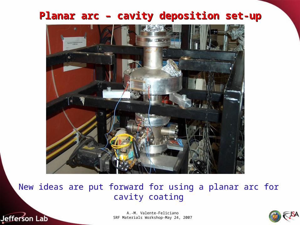
Planar arc – cavity deposition set-upPlanar arc – cavity deposition set-up
New ideas are put forward for using a planar arc for cavity coating
5 µm
10 µm

A.-M. Valente-FelicianoSRF Materials Workshop-May 24, 2007
Planar arc – RF measurements on samples!Planar arc – RF measurements on samples!
Cu samples with Nb ARC-coating. Used as a baseplate of 6 GHz cavity operating in the TE011 mode. At low field, the surface resistance is in the range 3÷6 µOhm, as compared to the BCS Rs of 0.22 µOhm at 2.2 K and small mean free path. The Q remained constant up to a field of 300 Oe.
A baseline of 2.2 µOhm is measured with this cavity with a solid Nb plateA. Romanenko and H. Padamsee, Proc. SRF2005, Cornell, USA, A. Romanenko and H. Padamsee, Proc. SRF2005, Cornell, USA,
20052005

A.-M. Valente-FelicianoSRF Materials Workshop-May 24, 2007
Liner arc for cavity deposition (Soltan Liner arc for cavity deposition (Soltan Institute)Institute)

A.-M. Valente-FelicianoSRF Materials Workshop-May 24, 2007
SUMMARYSUMMARY• Niobium thin film cavities require:
- m.f.p. >> coherence length
- surface roughness consistent with low magnetic field enhancement
- a surface free from fissures, enhanced grain boundary oxidation, etc.
• Features of energetic condensation systems:
- the upper limit on ion energy is bounded by the defect density created
- within the limits of cavity application, these films will be columnar
- good film structure can be obtained on amorphous substrates
- a RRR of at least 100 or more is desirable and a better understanding of defect sources is needed
- ion energy is limited by the reverse sputtering yield from the film to the point at which no net deposition occurs
- normal incidence is likely to produce less roughness