Multi-Level Inverters · „Multi-Level Inverters ... Three-Level Inverter 4 2 U Z 0Z U L 1 ......
34
Lecture Power Electronics „Multi-Level Inverters“ Prof. Dr.‐Ing. Ralph Kennel ([email protected]) Technische Universität München Electrical Drive Systems and Power Electronics Arcisstraße 21 80333 München Germany
Transcript of Multi-Level Inverters · „Multi-Level Inverters ... Three-Level Inverter 4 2 U Z 0Z U L 1 ......

LecturePower Electronics
„Multi-Level Inverters“
Prof. Dr.‐Ing. Ralph Kennel
Technische Universität München
Electrical Drive Systems and Power Electronics
Arcisstraße 21
80333 München
Germany
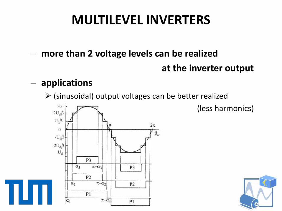
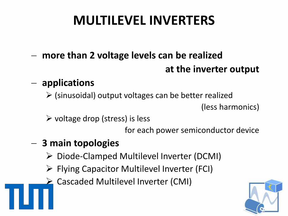
MULTILEVEL INVERTERS
more than 2 voltage levels can be realized
at the inverter output
applications
(sinusoidal) output voltages can be better realized
(less harmonics)
MULTILEVEL INVERTERS
more than 2 voltage levels can be realized
at the inverter output
applications (sinusoidal) output voltages can be better realized
(less harmonics)
voltage drop (stress) is less
for each power semiconductor device
3 main topologies Diode-Clamped Multilevel Inverter (DCMI)
Flying Capacitor Multilevel Inverter (FCI)
Cascaded Multilevel Inverter (CMI)

Three-Level Inverter
4
2
ZU
0
ZU
L1
Finer gradation of the output voltage
Reduction of the current ripple … or…
Reduction of the pulse frequency
Halving the voltage stress on thesemiconductor switches
Range of application: approx. 10 MW, 3.3 kV(Siemens, Simovert ML2, Rolling Technology)
IGCT switches
Origin : Dr.-Ing. Olaf Simon, SEW Eurodrive


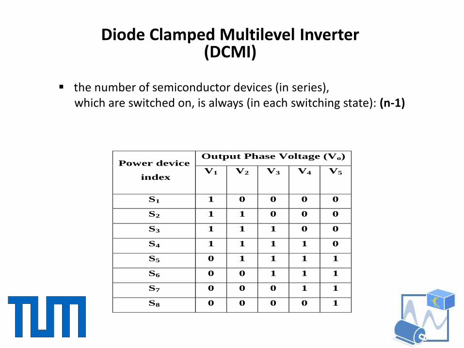
the number of semiconductor devices (in series),which are switched on, is always (in each switching state): (n-1)
Output Phase Voltage (Vo) Power device
index V1
V2
V3
V4
V5
S1 1 0 0 0 0
S2 1 1 0 0 0
S3 1 1 1 0 0
S4 1 1 1 1 0
S5 0 1 1 1 1
S6 0 0 1 1 1
S7 0 0 0 1 1
S8 0 0 0 0 1
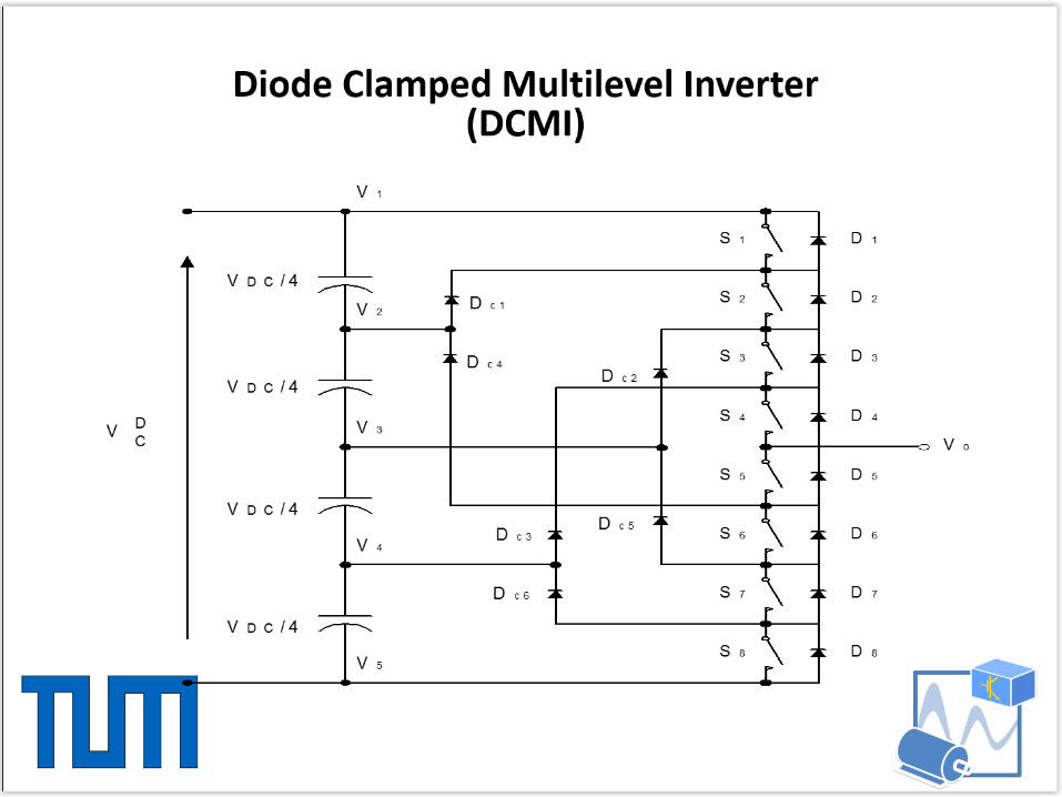
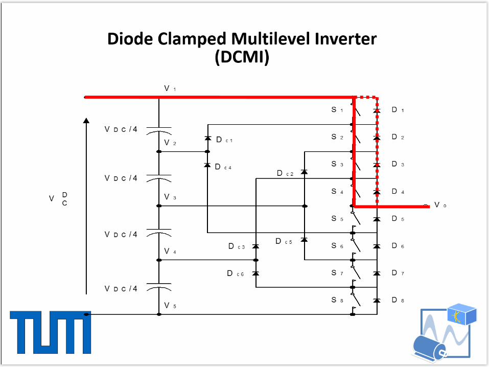
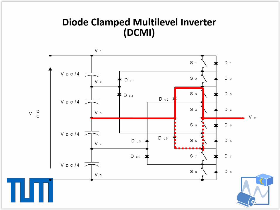
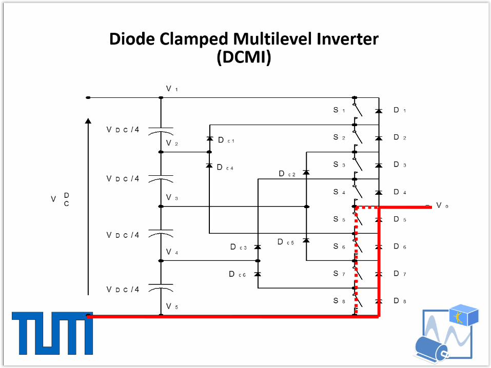
Diode Clamped Multilevel Inverter(DCMI)
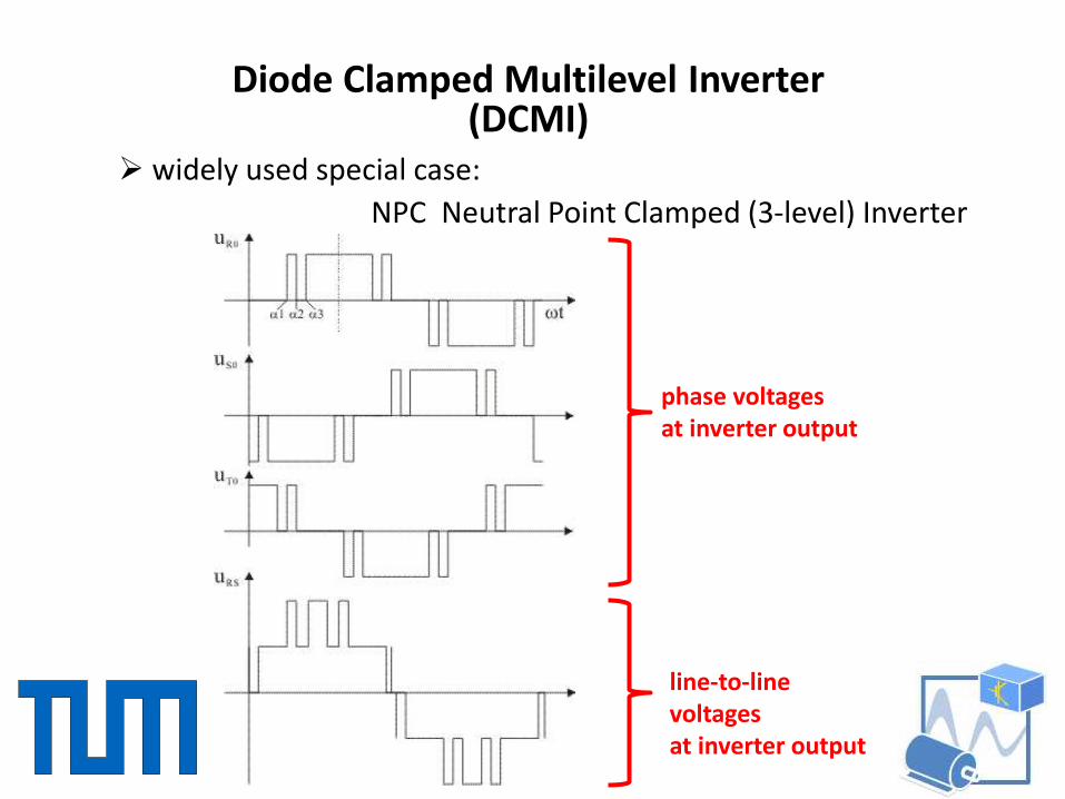
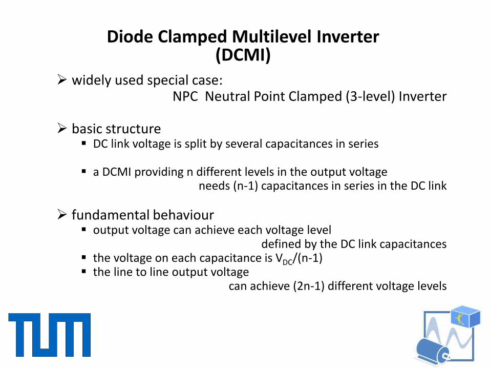
widely used special case:
NPC Neutral Point Clamped (3-level) Inverter
Diode Clamped Multilevel Inverter(DCMI)
phase voltagesat inverter output
line-to-linevoltagesat inverter output
widely used special case:NPC Neutral Point Clamped (3-level) Inverter
basic structure DC link voltage is split by several capacitances in series
a DCMI providing n different levels in the output voltageneeds (n-1) capacitances in series in the DC link
fundamental behaviour output voltage can achieve each voltage level
defined by the DC link capacitances the voltage on each capacitance is VDC/(n-1) the line to line output voltage
can achieve (2n-1) different voltage levels
Diode Clamped Multilevel Inverter(DCMI)
Diode Clamped Multilevel Inverter(DCMI)
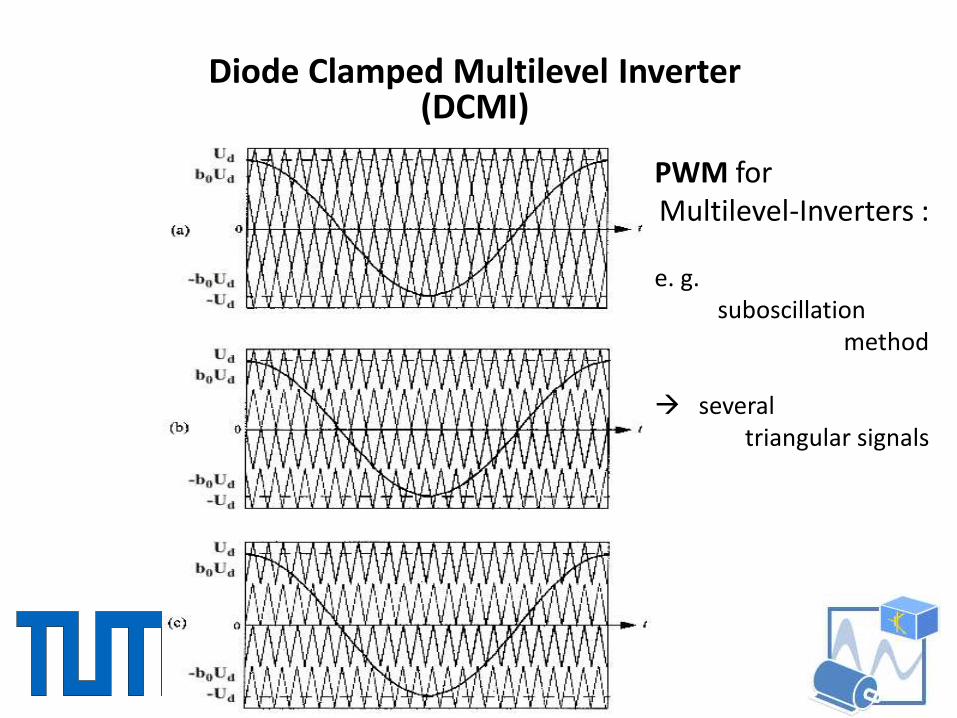
PWM forMultilevel-Inverters :
e. g.suboscillation
method
severaltriangular signals
In combination with specific PWM schemes, there might occur
instabilities in the equal distribution of DC link voltage
to the DC link capacitances (balancing)
the average current to the inner knots of the DC link
might not be 0 within a PWM cycle
in case of space vector modulation and inductive load,
this problem is of minor importance
solution of this problem adapted PWM scheme - adapted use of zero vectors ...
... for capacitor voltage control (balancing)
Diode Clamped Multilevel Inverter(DCMI)
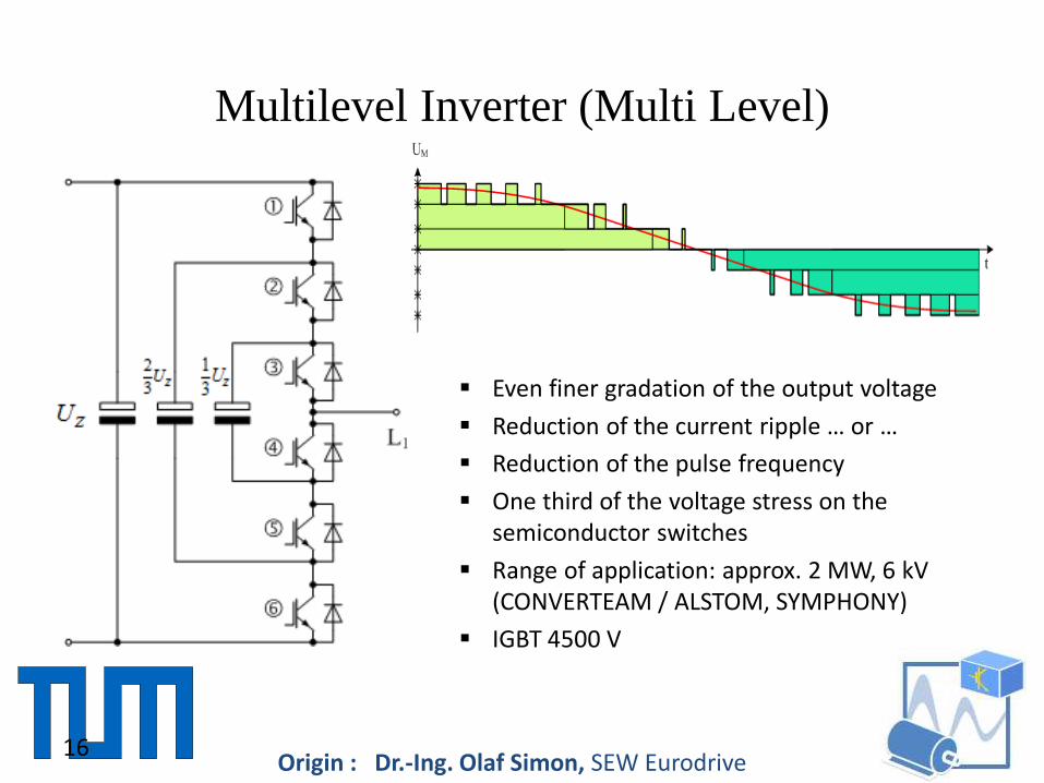
Multilevel Inverter (Multi Level)
16
Even finer gradation of the output voltage
Reduction of the current ripple … or …
Reduction of the pulse frequency
One third of the voltage stress on thesemiconductor switches
Range of application: approx. 2 MW, 6 kV(CONVERTEAM / ALSTOM, SYMPHONY)
IGBT 4500 V
Origin : Dr.-Ing. Olaf Simon, SEW Eurodrive
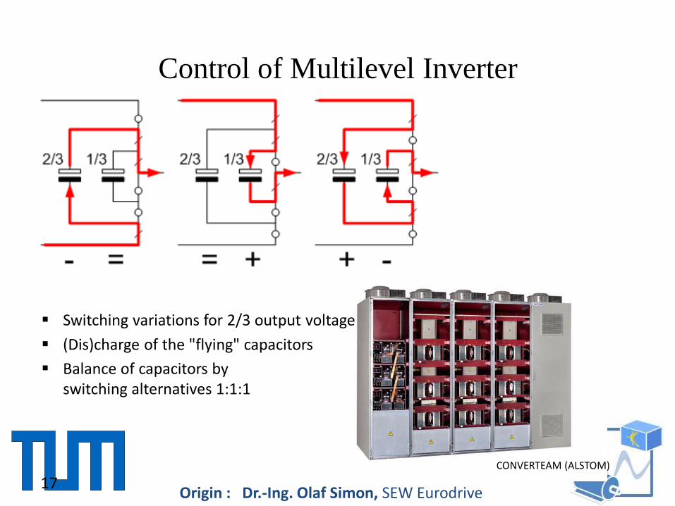
Control of Multilevel Inverter
17
Switching variations for 2/3 output voltage
(Dis)charge of the "flying" capacitors
Balance of capacitors byswitching alternatives 1:1:1
CONVERTEAM (ALSTOM)
Origin : Dr.-Ing. Olaf Simon, SEW Eurodrive

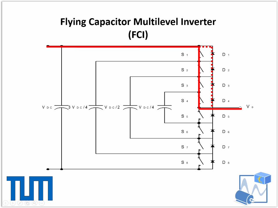

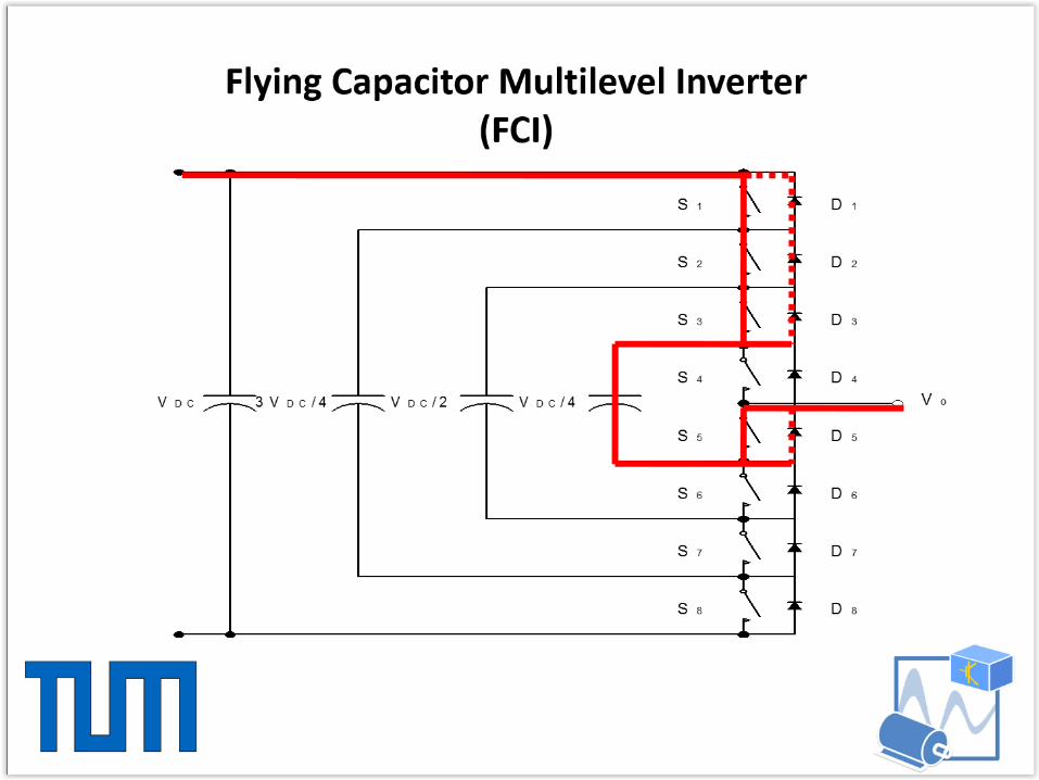
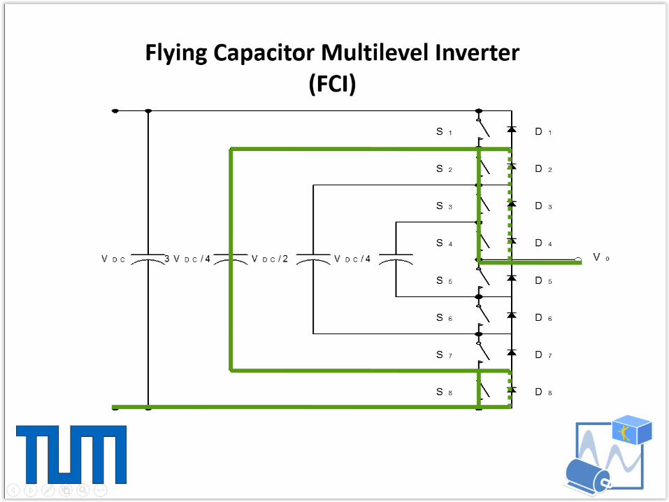
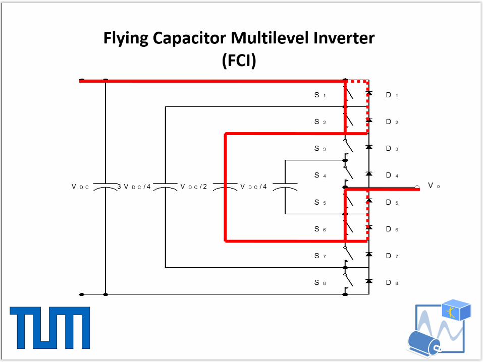

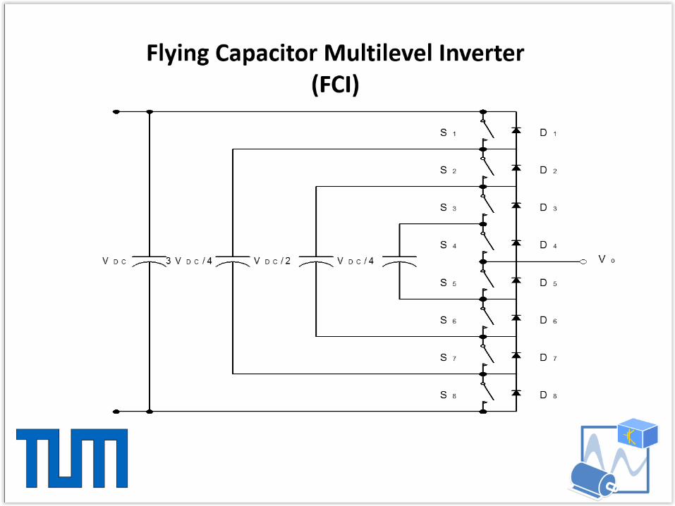

Flying Capacitor Multilevel Inverter(FCI)
possible space phasors (space vectors)
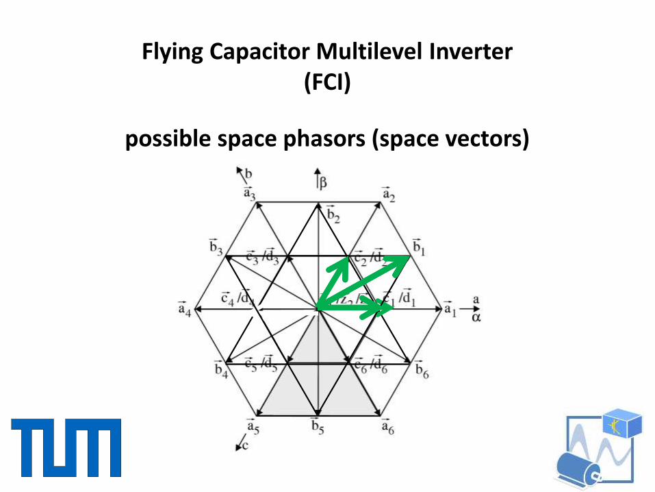
Flying Capacitor Multilevel Inverter(FCI)
possible space phasors (space vectors)
Flying Capacitor Multilevel Inverter(FCI)
number of diodes is significantly lower than in a DCMI
voltage potential of the (“flying”) capacitors
is floating with reference to the ground potential
balanced distribution of DC link voltage
to the DC link capacitors (balancing)
is not a problem with FCI
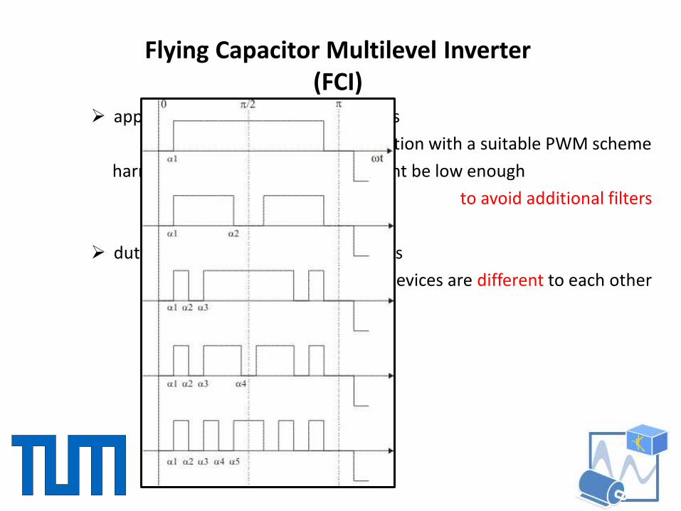
applying a sufficient number of levels
in combination with a suitable PWM scheme
harmonics in the output voltage might be low enough
to avoid additional filters
duty cycles and switching frequencies
of power semiconductor devices are different to each other
Flying Capacitor Multilevel Inverter(FCI)
applying a sufficient number of levels
in combination with a suitable PWM scheme
harmonics in the output voltage might be low enough
to avoid additional filters
duty cycles and switching frequencies
of power semiconductor devices are different to each other
Flying Capacitor Multilevel Inverter(FCI)
applying a sufficient number of levels
in combination with a suitable PWM scheme
harmonics in the output voltage might be low enough
to avoid additional filters
duty cycles and switching frequencies
of power semiconductor devices are different to each other
additional provisions/strategies are necessary
for charging the DC link capacitors
Flying Capacitor Multilevel Inverter(FCI)
Vphase (Vo)
S11 S21
S31 S41
S1h S2h
S3h S4h
S12 S22
S32 S42
VDC
Module 1
Module 2
Module h
Vm1
0
VDC
VDC
Vm2
Vmh
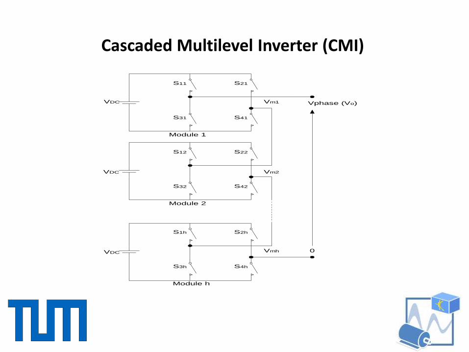
Cascaded Multilevel Inverter (CMI)
also known as
Cascaded Multi-Level Inverter with separat DC links
or as inverter bridges in series connection
simple and modular design
needs lowest number of power semiconductor devices
needs several DC links isolated against each other
Cascaded Multilevel Inverter (CMI)
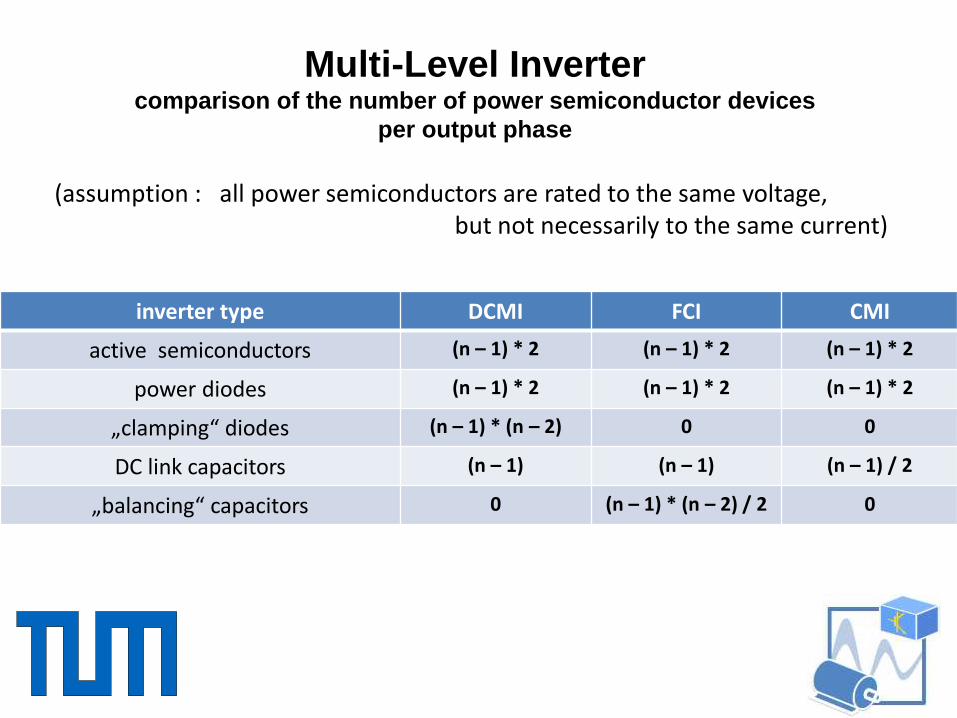
Multi-Level Invertercomparison of the number of power semiconductor devices
per output phase
(assumption : all power semiconductors are rated to the same voltage,but not necessarily to the same current)
inverter type DCMI FCI CMI
active semiconductors (n – 1) * 2 (n – 1) * 2 (n – 1) * 2
power diodes (n – 1) * 2 (n – 1) * 2 (n – 1) * 2
„clamping“ diodes (n – 1) * (n – 2) 0 0
DC link capacitors (n – 1) (n – 1) (n – 1) / 2
„balancing“ capacitors 0 (n – 1) * (n – 2) / 2 0


![[PPT]Three-Phase Inverters - Welcome - Faculty Pages - … · Web viewThree-Phase Inverters Consider three single-phase inverters in parallel, driven 120 apart. Three-Phase Inverter](https://static.fdocuments.in/doc/165x107/5b08de6f7f8b9a520e8d510f/pptthree-phase-inverters-welcome-faculty-pages-viewthree-phase-inverters.jpg)