Solving Harmonic Elimination Equations in Multi-level Inverters by using Neural Networks

8/8/2019 InverterTwo-Level Inverters
http://slidepdf.com/reader/full/invertertwo-level-inverters 1/8
IEEE TRANSACTIONS ON INDUSTRIAL ELECTRONICS, VOL. 57, NO. 11, NOVEMBER 2010 3707
A Hybrid Multilevel Inverter Topology for anOpen-End Winding Induction-Motor Drive
Using Two-Level Inverters in SeriesWith a Capacitor-Fed H-Bridge CellK. Sivakumar, Student Member, IEEE , Anandarup Das, Student Member, IEEE ,
Rijil Ramchand, Student Member, IEEE , Chintan Patel, Student Member, IEEE , andK. Gopakumar, Senior Member, IEEE
Abstract—In this paper, a new five-level inverter topology foropen-end winding induction-motor (IM) drive is proposed. Theopen-end winding IM is fed from one end with a two-level inverterin series with a capacitor-fed H-bridge cell, while the other end
is connected to a conventional two-level inverter. The combinedinverter system produces voltage space-vector locations identicalto that of a conventional five-level inverter. A total of 2744 space-vector combinations are distributed over 61 space-vector locationsin the proposed scheme. With such a high number of switchingstate redundancies, it is possible to balance the H-bridge capacitorvoltages under all operating conditions including overmodulationregion. In addition to that, the proposed topology eliminates 18clamping diodes having different voltage ratings compared withthe neutral point clamped inverter. On the other hand, it requiresonly one capacitor bank per phase, whereas the flying-capacitorscheme for a five-level topology requires more than one capacitorbank per phase. The proposed inverter topology can be operatedas a three-level inverter for full modulation range, in case of any switch failure in the capacitor-fed H-bridge cell. This will
increase the reliability of the system. The proposed scheme isexperimentally verified on a four-pole 5-hp IM drive.
Index Terms—H-bridge, multilevel inverter, open-end windinginduction motor (IM) drive.
I. INTRODUCTION
M ULTILEVEL voltage-source inverters have been receiv-
ing more and more attention in the past few years for
high- and medium-power induction-motor (IM) drive applica-
tions. Many multilevel inverter configurations and pulsewidth
modulation (PWM) techniques are presented to improve the
output voltage harmonic spectrum [1], [3]–[5]. Some of the
popular multilevel configurations are the neutral point clamped
(NPC), series-connected H-bridge, flying capacitor, etc.
Although they can be configured for more than two levels,
as the number of levels increase, the power circuit and con-
trol complexity due to a large number of devices, increases.
An optimum topology for multilevel inverters for more than
three levels has not been achieved until now, and research is
Manuscript received June 11, 2009; revised August 26, 2009, October 19,2009, and November 30, 2009; accepted December 17, 2009. Date of publica-tion February 8, 2010; date of current version October 13, 2010.
The authors are with the Center for Electronics Design and Technology,Indian Institute of Science, Bangalore 560 012, India (e-mail: [email protected]).
Digital Object Identifier 10.1109/TIE.2010.2040565
going on to improve the drive efficiency at reduced circuit
complexity and control. In NPC multilevel inverters [1]–[7],
the load current drawn from the neutral point will cause an
unequal voltage sharing between the series-connected capac-
itors. This will introduce unwanted harmonics in the inverteroutput voltage and also results in an unequal voltage stress on
the switching devices. To avoid this problem, special voltage-
balancing techniques must be implemented [2], [5]–[7], or
isolated voltage sources have to supply each series-connected
capacitors. Although a scheme is proposed in [8] that allows the
NPC three-level inverter to operate with unbalanced capacitor
voltages, it increases the control-circuit complexity due to the
3-D space-vector arrangement. In cascaded H-bridge (CHB)
multilevel inverter structure [9]–[11], the H-bridge cells are
supplied from individual dc source and are series connected
to generate multilevel voltage profile. As the number of levels
increases, the CHB requires a huge number of isolated voltagesources. In a flying-capacitor topology [12], more number of
levels in the phase voltage is generated by adding or sub-
tracting the capacitor voltages. It requires additional control
and increased switching for maintaining the capacitor voltages
constant. The power circuit and control complexity increases
when the number of levels increases in the output voltage. The
generalized multilevel inverter topology is presented in [13].
This topology is a combination of NPC and flying-capacitor
inverter topologies. However, it requires additional capacitor
banks and many active switches to generate a multilevel out-
put voltage. A hybrid asymmetric multilevel inverter topology
is proposed [14], by connecting a flying capacitor in serieswith the NPC inverter. However, this scheme is not valid
for the entire operating range of the drive (with respect to
the power factor and modulation index). A dc-voltage-ratio
control strategy for single-phase two-cell CHB converter with
a single dc source is presented in [15]. However, this scheme
is based on the elimination of switching states which tend to
make the floating capacitor voltage unbalanced. Therefore, this
scheme cannot be operated for the full modulation range using
any arbitrary dc-voltage ratios (i.e., the ratio between the dc-
source voltage and floating-capacitor voltage). Moreover, if this
scheme is extended to a three-phase system, then it requires
three isolated voltage sources.
0278-0046/$26.00 © 2010 IEEE
8/8/2019 InverterTwo-Level Inverters
http://slidepdf.com/reader/full/invertertwo-level-inverters 2/8
3708 IEEE TRANSACTIONS ON INDUSTRIAL ELECTRONICS, VOL. 57, NO. 11, NOVEMBER 2010
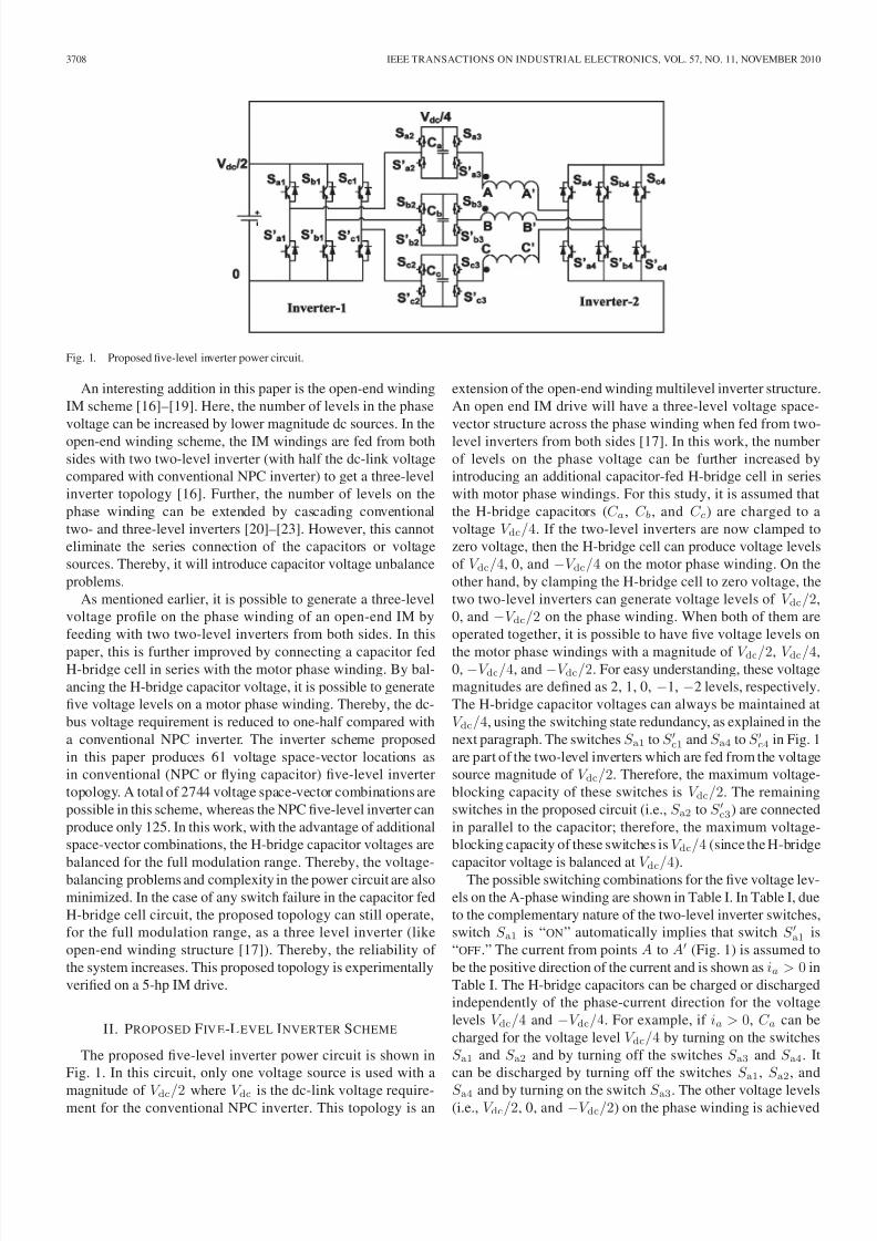
Fig. 1. Proposed five-level inverter power circuit.
An interesting addition in this paper is the open-end winding
IM scheme [16]–[19]. Here, the number of levels in the phase
voltage can be increased by lower magnitude dc sources. In the
open-end winding scheme, the IM windings are fed from both
sides with two two-level inverter (with half the dc-link voltage
compared with conventional NPC inverter) to get a three-level
inverter topology [16]. Further, the number of levels on the
phase winding can be extended by cascading conventional
two- and three-level inverters [20]–[23]. However, this cannot
eliminate the series connection of the capacitors or voltage
sources. Thereby, it will introduce capacitor voltage unbalance
problems.
As mentioned earlier, it is possible to generate a three-level
voltage profile on the phase winding of an open-end IM by
feeding with two two-level inverters from both sides. In this
paper, this is further improved by connecting a capacitor fedH-bridge cell in series with the motor phase winding. By bal-
ancing the H-bridge capacitor voltage, it is possible to generate
five voltage levels on a motor phase winding. Thereby, the dc-
bus voltage requirement is reduced to one-half compared with
a conventional NPC inverter. The inverter scheme proposed
in this paper produces 61 voltage space-vector locations as
in conventional (NPC or flying capacitor) five-level inverter
topology. A total of 2744 voltage space-vector combinations are
possible in this scheme, whereas the NPC five-level inverter can
produce only 125. In this work, with the advantage of additional
space-vector combinations, the H-bridge capacitor voltages are
balanced for the full modulation range. Thereby, the voltage-
balancing problems and complexity in the power circuit are also
minimized. In the case of any switch failure in the capacitor fed
H-bridge cell circuit, the proposed topology can still operate,
for the full modulation range, as a three level inverter (like
open-end winding structure [17]). Thereby, the reliability of
the system increases. This proposed topology is experimentally
verified on a 5-hp IM drive.
II. PROPOSED FIV E-L EVEL INVERTER SCHEME
The proposed five-level inverter power circuit is shown in
Fig. 1. In this circuit, only one voltage source is used with a
magnitude of V dc/2 where V dc is the dc-link voltage require-ment for the conventional NPC inverter. This topology is an
extension of the open-end winding multilevel inverter structure.
An open end IM drive will have a three-level voltage space-
vector structure across the phase winding when fed from two-
level inverters from both sides [17]. In this work, the number
of levels on the phase voltage can be further increased by
introducing an additional capacitor-fed H-bridge cell in series
with motor phase windings. For this study, it is assumed that
the H-bridge capacitors (C a, C b, and C c) are charged to a
voltage V dc/4. If the two-level inverters are now clamped to
zero voltage, then the H-bridge cell can produce voltage levels
of V dc/4, 0, and −V dc/4 on the motor phase winding. On the
other hand, by clamping the H-bridge cell to zero voltage, the
two two-level inverters can generate voltage levels of V dc/2,
0, and −V dc/2 on the phase winding. When both of them are
operated together, it is possible to have five voltage levels on
the motor phase windings with a magnitude of V dc/2, V dc/4,0, −V dc/4, and −V dc/2. For easy understanding, these voltage
magnitudes are defined as 2, 1, 0, −1, −2 levels, respectively.
The H-bridge capacitor voltages can always be maintained at
V dc/4, using the switching state redundancy, as explained in the
next paragraph. The switches S a1 to S c1 and S a4 to S c4 in Fig. 1
are part of the two-level inverters which are fed from the voltage
source magnitude of V dc/2. Therefore, the maximum voltage-
blocking capacity of these switches is V dc/2. The remaining
switches in the proposed circuit (i.e., S a2 to S c3) are connected
in parallel to the capacitor; therefore, the maximum voltage-
blocking capacity of these switches isV dc/4 (since the H-bridge
capacitor voltage is balanced atV dc
/4).
The possible switching combinations for the five voltage lev-
els on the A-phase winding are shown in Table I. In Table I, due
to the complementary nature of the two-level inverter switches,
switch S a1 is “ON” automatically implies that switch S a1 is
“OFF.” The current from points A to A (Fig. 1) is assumed to
be the positive direction of the current and is shown as ia > 0 in
Table I. The H-bridge capacitors can be charged or discharged
independently of the phase-current direction for the voltage
levels V dc/4 and −V dc/4. For example, if ia > 0, C a can be
charged for the voltage level V dc/4 by turning on the switches
S a1 and S a2 and by turning off the switches S a3 and S a4. It
can be discharged by turning off the switches S a1, S a2, and
S a4 and by turning on the switch S a3. The other voltage levels(i.e., V dc/2, 0, and −V dc/2) on the phase winding is achieved
8/8/2019 InverterTwo-Level Inverters
http://slidepdf.com/reader/full/invertertwo-level-inverters 3/8
SIVAKUMAR et al.: HYBRID MULTILEVEL INVERTER TOPOLOGY FOR OPEN-END WINDING IM DRIVE 3709
TABLE IALL POSSIBLE SWITCHING COMBINATIONS FOR THE FIV E VOLTAGE LEVELS FOR PHASE A
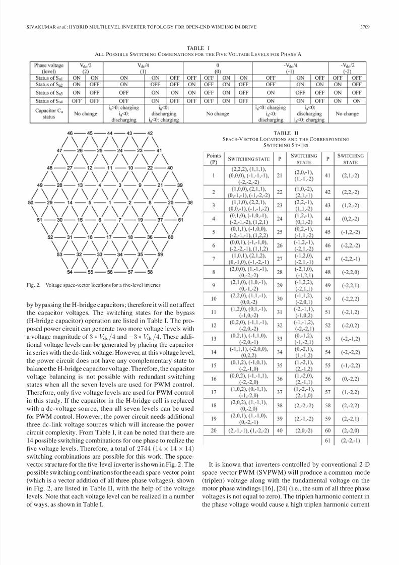
Fig. 2. Voltage space-vector locations for a five-level inverter.
by bypassing the H-bridge capacitors; therefore it will not affect
the capacitor voltages. The switching states for the bypass
(H-bridge capacitor) operation are listed in Table I. The pro-
posed power circuit can generate two more voltage levels with
a voltage magnitude of 3 ∗ V dc/4 and −3 ∗ V dc/4. These addi-
tional voltage levels can be generated by placing the capacitor
in series with the dc-link voltage. However, at this voltage level,
the power circuit does not have any complementary state to
balance the H-bridge capacitor voltage. Therefore, the capacitor
voltage balancing is not possible with redundant switching
states when all the seven levels are used for PWM control.
Therefore, only five voltage levels are used for PWM controlin this study. If the capacitor in the H-bridge cell is replaced
with a dc-voltage source, then all seven levels can be used
for PWM control. However, the power circuit needs additional
three dc-link voltage sources which will increase the power
circuit complexity. From Table I, it can be noted that there are
14 possible switching combinations for one phase to realize the
five voltage levels. Therefore, a total of 2744 (14 × 14 × 14)switching combinations are possible for this work. The space-
vector structure for the five-level inverter is shown in Fig. 2. The
possible switching combinations for the each space-vector point
(which is a vector addition of all three-phase voltages), shown
in Fig. 2, are listed in Table II, with the help of the voltage
levels. Note that each voltage level can be realized in a numberof ways, as shown in Table I.
TABLE IISPACE-V ECTOR LOCATIONS AND THE CORRESPONDING
SWITCHING STATES
It is known that inverters controlled by conventional 2-D
space-vector PWM (SVPWM) will produce a common-mode
(triplen) voltage along with the fundamental voltage on the
motor phase windings [16], [24] (i.e., the sum of all three phase
voltages is not equal to zero). The triplen harmonic content inthe phase voltage would cause a high triplen harmonic current
8/8/2019 InverterTwo-Level Inverters
http://slidepdf.com/reader/full/invertertwo-level-inverters 4/8
3710 IEEE TRANSACTIONS ON INDUSTRIAL ELECTRONICS, VOL. 57, NO. 11, NOVEMBER 2010
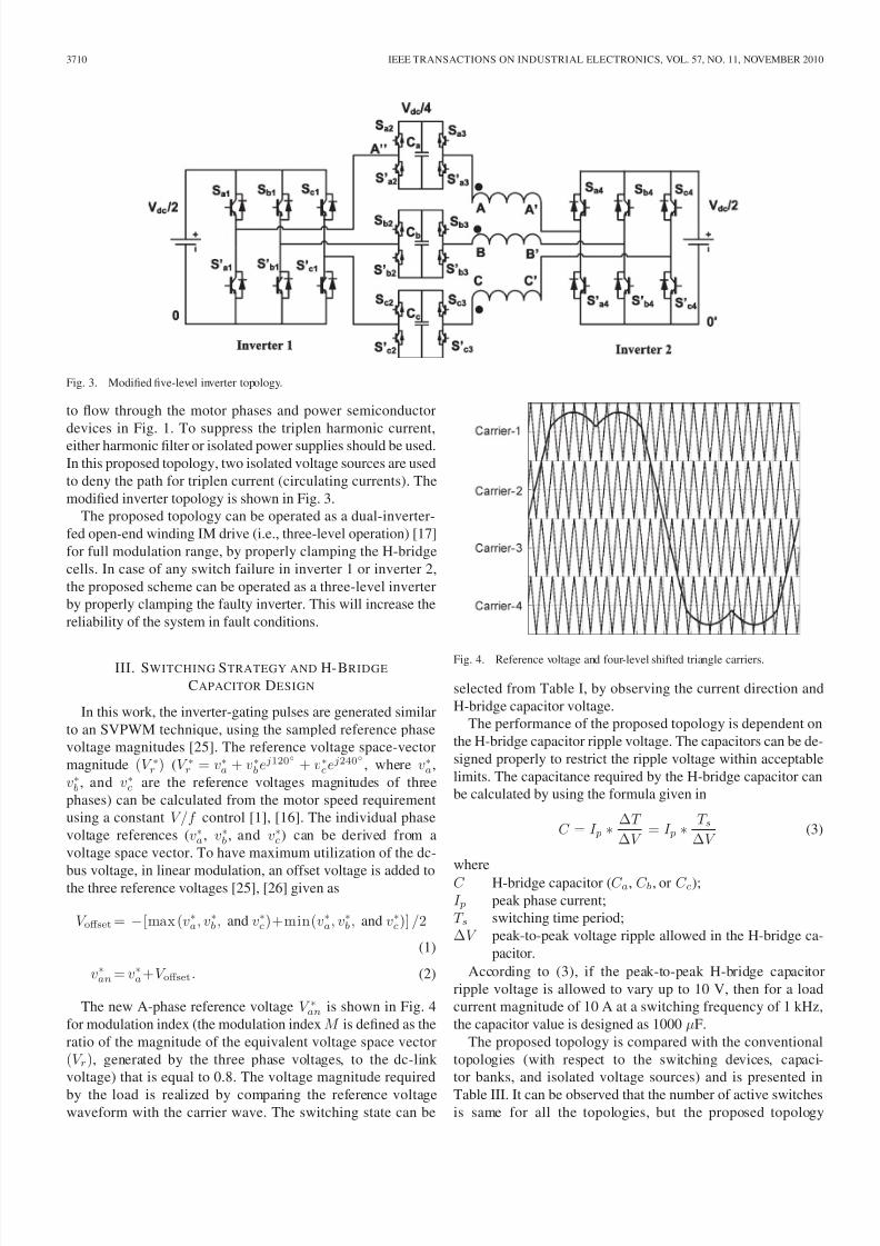
Fig. 3. Modified five-level inverter topology.
to flow through the motor phases and power semiconductor
devices in Fig. 1. To suppress the triplen harmonic current,
either harmonic filter or isolated power supplies should be used.
In this proposed topology, two isolated voltage sources are used
to deny the path for triplen current (circulating currents). The
modified inverter topology is shown in Fig. 3.
The proposed topology can be operated as a dual-inverter-
fed open-end winding IM drive (i.e., three-level operation) [17]
for full modulation range, by properly clamping the H-bridge
cells. In case of any switch failure in inverter 1 or inverter 2,
the proposed scheme can be operated as a three-level inverter
by properly clamping the faulty inverter. This will increase the
reliability of the system in fault conditions.
III. SWITCHING STRATEGY AND H-BRIDGE
CAPACITOR DESIGN
In this work, the inverter-gating pulses are generated similar
to an SVPWM technique, using the sampled reference phase
voltage magnitudes [25]. The reference voltage space-vector
magnitude (V ∗r ) (V ∗r = v∗a + v∗bej120◦ + v∗ce
j240◦ , where v∗a,
v∗b , and v∗c are the reference voltages magnitudes of three
phases) can be calculated from the motor speed requirement
using a constant V/f control [1], [16]. The individual phase
voltage references (v∗a, v∗b , and v∗c) can be derived from a
voltage space vector. To have maximum utilization of the dc-
bus voltage, in linear modulation, an offset voltage is added tothe three reference voltages [25], [26] given as
V offset= −[max (v∗a, v∗
b, and v∗c)+min(v∗a, v∗
b, and v∗c)] /2
(1)
v∗an = v∗a+V offset. (2)
The new A-phase reference voltage V ∗an is shown in Fig. 4
for modulation index (the modulation index M is defined as the
ratio of the magnitude of the equivalent voltage space vector
(V r), generated by the three phase voltages, to the dc-link
voltage) that is equal to 0.8. The voltage magnitude required
by the load is realized by comparing the reference voltagewaveform with the carrier wave. The switching state can be
Fig. 4. Reference voltage and four-level shifted triangle carriers.
selected from Table I, by observing the current direction and
H-bridge capacitor voltage.
The performance of the proposed topology is dependent on
the H-bridge capacitor ripple voltage. The capacitors can be de-
signed properly to restrict the ripple voltage within acceptable
limits. The capacitance required by the H-bridge capacitor can
be calculated by using the formula given in
C = I p ∗ΔT
ΔV = I p ∗
T sΔV
(3)
where
C H-bridge capacitor (C a, C b, or C c);
I p peak phase current;
T s switching time period;
ΔV peak-to-peak voltage ripple allowed in the H-bridge ca-
pacitor.
According to (3), if the peak-to-peak H-bridge capacitor
ripple voltage is allowed to vary up to 10 V, then for a load
current magnitude of 10 A at a switching frequency of 1 kHz,
the capacitor value is designed as 1000 μF.
The proposed topology is compared with the conventional
topologies (with respect to the switching devices, capaci-
tor banks, and isolated voltage sources) and is presented in
Table III. It can be observed that the number of active switchesis same for all the topologies, but the proposed topology
8/8/2019 InverterTwo-Level Inverters
http://slidepdf.com/reader/full/invertertwo-level-inverters 5/8
SIVAKUMAR et al.: HYBRID MULTILEVEL INVERTER TOPOLOGY FOR OPEN-END WINDING IM DRIVE 3711
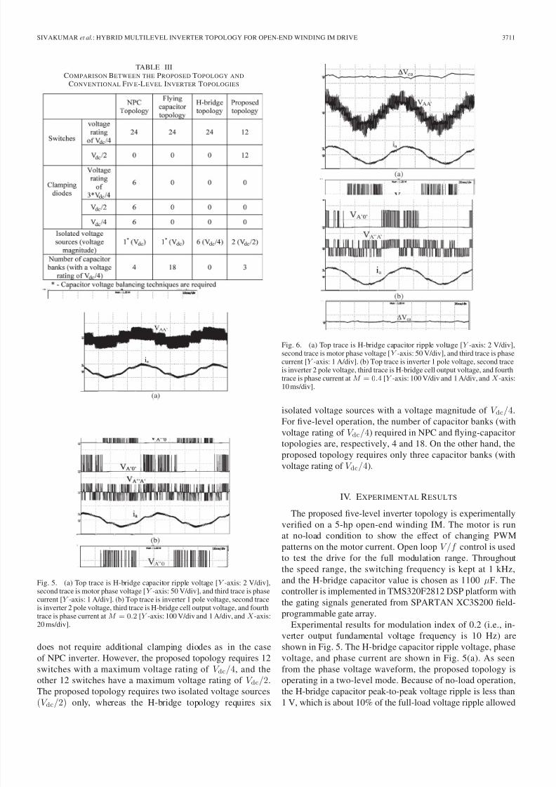
TABLE IIICOMPARISON BETWEEN THE PROPOSED TOPOLOGY AND
CONVENTIONAL FIV E-L EVEL INVERTER TOPOLOGIES
Fig. 5. (a) Top trace is H-bridge capacitor ripple voltage [Y -axis: 2 V/div],second trace is motor phase voltage [Y -axis: 50 V/div], and third trace is phasecurrent [Y -axis: 1 A/div]. (b) Top trace is inverter 1 pole voltage, second traceis inverter 2 pole voltage, third trace is H-bridge cell output voltage, and fourthtrace is phase current at M = 0.2 [Y -axis: 100 V/div and 1 A/div, and X-axis:20 ms/div].
does not require additional clamping diodes as in the case
of NPC inverter. However, the proposed topology requires 12
switches with a maximum voltage rating of V dc/4, and the
other 12 switches have a maximum voltage rating of V dc/2.
The proposed topology requires two isolated voltage sources(V dc/2) only, whereas the H-bridge topology requires six
Fig. 6. (a) Top trace is H-bridge capacitor ripple voltage [Y -axis: 2 V/div],second trace is motor phase voltage [Y -axis: 50 V/div], and third trace is phasecurrent [Y -axis: 1 A/div]. (b) Top trace is inverter 1 pole voltage, second traceis inverter 2 pole voltage, third trace is H-bridge cell output voltage, and fourthtrace is phase current at M = 0.4 [Y -axis: 100 V/div and 1 A/div, and X-axis:10 ms/div].
isolated voltage sources with a voltage magnitude of V dc/4.For five-level operation, the number of capacitor banks (with
voltage rating of V dc/4) required in NPC and flying-capacitor
topologies are, respectively, 4 and 18. On the other hand, the
proposed topology requires only three capacitor banks (with
voltage rating of V dc/4).
IV. EXPERIMENTAL RESULTS
The proposed five-level inverter topology is experimentally
verified on a 5-hp open-end winding IM. The motor is run
at no-load condition to show the effect of changing PWM
patterns on the motor current. Open loop V/f control is usedto test the drive for the full modulation range. Throughout
the speed range, the switching frequency is kept at 1 kHz,
and the H-bridge capacitor value is chosen as 1100 μF. The
controller is implemented in TMS320F2812 DSP platform with
the gating signals generated from SPARTAN XC3S200 field-
programmable gate array.
Experimental results for modulation index of 0.2 (i.e., in-
verter output fundamental voltage frequency is 10 Hz) are
shown in Fig. 5. The H-bridge capacitor ripple voltage, phase
voltage, and phase current are shown in Fig. 5(a). As seen
from the phase voltage waveform, the proposed topology is
operating in a two-level mode. Because of no-load operation,
the H-bridge capacitor peak-to-peak voltage ripple is less than1 V, which is about 10% of the full-load voltage ripple allowed
8/8/2019 InverterTwo-Level Inverters
http://slidepdf.com/reader/full/invertertwo-level-inverters 6/8
3712 IEEE TRANSACTIONS ON INDUSTRIAL ELECTRONICS, VOL. 57, NO. 11, NOVEMBER 2010
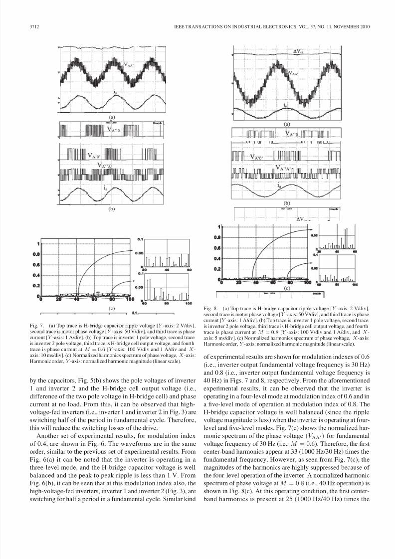
Fig. 7. (a) Top trace is H-bridge capacitor ripple voltage [Y -axis: 2 V/div],second trace is motor phase voltage [Y -axis: 50 V/div], and third trace is phasecurrent [Y -axis: 1 A/div]. (b) Top trace is inverter 1 pole voltage, second traceis inverter 2 pole voltage, third trace is H-bridge cell output voltage, and fourthtrace is phase current at M = 0.6 [Y -axis: 100 V/div and 1 A/div and X-axis: 10 ms/div]. (c) Normalized harmonics spectrum of phase voltage, X-axis:Harmonic order, Y -axis: normalized harmonic magnitude (linear scale).
by the capacitors. Fig. 5(b) shows the pole voltages of inverter
1 and inverter 2 and the H-bridge cell output voltage (i.e.,difference of the two pole voltage in H-bridge cell) and phase
current at no load. From this, it can be observed that high-
voltage-fed inverters (i.e., inverter 1 and inverter 2 in Fig. 3) are
switching half of the period in fundamental cycle. Therefore,
this will reduce the switching losses of the drive.
Another set of experimental results, for modulation index
of 0.4, are shown in Fig. 6. The waveforms are in the same
order, similar to the previous set of experimental results. From
Fig. 6(a) it can be noted that the inverter is operating in a
three-level mode, and the H-bridge capacitor voltage is well
balanced and the peak to peak ripple is less than 1 V. From
Fig. 6(b), it can be seen that at this modulation index also, the
high-voltage-fed inverters, inverter 1 and inverter 2 (Fig. 3), areswitching for half a period in a fundamental cycle. Similar kind
Fig. 8. (a) Top trace is H-bridge capacitor ripple voltage [Y -axis: 2 V/div],second trace is motor phase voltage [Y -axis: 50 V/div], and third trace is phasecurrent [Y -axis: 1 A/div]. (b) Top trace is inverter 1 pole voltage, second traceis inverter 2 pole voltage, third trace is H-bridge cell output voltage, and fourthtrace is phase current at M = 0.8 [Y -axis: 100 V/div and 1 A/div, and X-axis: 5 ms/div]. (c) Normalized harmonics spectrum of phase voltage, X-axis:Harmonic order, Y -axis: normalized harmonic magnitude (linear scale).
of experimental results are shown for modulation indexes of 0.6
(i.e., inverter output fundamental voltage frequency is 30 Hz)
and 0.8 (i.e., inverter output fundamental voltage frequency is
40 Hz) in Figs. 7 and 8, respectively. From the aforementioned
experimental results, it can be observed that the inverter isoperating in a four-level mode at modulation index of 0.6 and in
a five-level mode of operation at modulation index of 0.8. The
H-bridge capacitor voltage is well balanced (since the ripple
voltage magnitude is less) when the inverter is operating at four-
level and five-level modes. Fig. 7(c) shows the normalized har-
monic spectrum of the phase voltage (V AA) for fundamental
voltage frequency of 30 Hz (i.e., M = 0.6). Therefore, the first
center-band harmonics appear at 33 (1000 Hz/30 Hz) times the
fundamental frequency. However, as seen from Fig. 7(c), the
magnitudes of the harmonics are highly suppressed because of
the four-level operation of the inverter. A normalized harmonic
spectrum of phase voltage at M = 0.8 (i.e., 40 Hz operation) is
shown in Fig. 8(c). At this operating condition, the first center-band harmonics is present at 25 (1000 Hz/40 Hz) times the
8/8/2019 InverterTwo-Level Inverters
http://slidepdf.com/reader/full/invertertwo-level-inverters 7/8
SIVAKUMAR et al.: HYBRID MULTILEVEL INVERTER TOPOLOGY FOR OPEN-END WINDING IM DRIVE 3713
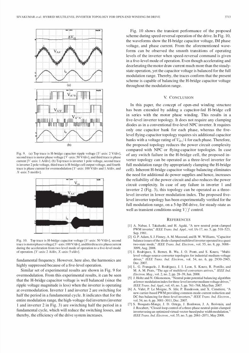
Fig. 9. (a) Top trace is H-bridge capacitor ripple voltage [Y -axis: 2 V/div],second trace is motor phase voltage [Y -axis: 50 V/div], and third trace is phasecurrent [Y -axis: 1 A/div]. (b) Top trace is inverter 1 pole voltage, second traceis inverter 2 pole voltage, third trace is H-bridge cell output voltage, and fourthtrace is phase current for overmodulation [Y -axis: 100 V/div and 1 A/div, andX-axis: 5 ms/div].
Fig. 10. Top trace is H-bridge capacitor voltage [Y -axis: 50 V/div], secondtrace is motorphasevoltage[Y -axis:100 V/div], andthirdtraceis phasecurrent
during the acceleration from two level mode of operation to a five-level modeof operation. [Y -axis: 2 A/div, X-axis: 5 s/div].
fundamental frequency. However, here also, the harmonics are
highly suppressed because of a five-level operation.
Similar set of experimental results are shown in Fig. 9 for
overmodulation. From this experimental results, it can be seen
that the H-bridge capacitor voltage is well balanced (since the
ripple voltage magnitude is less) when the inverter is operating
at overmodulation. Inverter 1 and inverter 2 are switching for
half the period in a fundamental cycle. It indicates that for the
entire modulation range, the high-voltage-fed inverters (inverter
1 and inverter 2 in Fig. 3) are switching half the period in a
fundamental cycle, which will reduce the switching losses, andthereby, the efficiency of the drive system increases.
Fig. 10 shows the transient performance of the proposed
scheme during speed-reversal operation of the drive. In Fig. 10,
the waveforms show the H-bridge capacitor voltage, IM phase
voltage, and phase current. From the aforementioned wave-
forms can be observed the smooth transitions of operating
levels of the inverter when speed-reversal command is given
in a five-level mode of operation. Even though accelerating anddecelerating the motor draw current much more than the steady-
state operation, yet the capacitor voltage is balanced for the full
modulation range. Thereby, the traces conform that the present
scheme is capable of balancing the H-bridge capacitor voltage
throughout the modulation range.
V. CONCLUSION
In this paper, the concept of open-end winding structure
has been extended by adding a capacitor-fed H-bridge cell
in series with the motor phase winding. This results in a
five-level inverter topology. It does not require any clamping
diodes as in a conventional five-level NPC inverter. It requiresonly one capacitor bank for each phase, whereas the five-
level flying-capacitor topology requires six additional capacitor
banks with a voltage rating of V dc/4 for each phase. Therefore,
the proposed topology reduces the power circuit complexity
compared with NPC or flying-capacitor topologies. In case
of any switch failure in the H-bridge cell, the proposed in-
verter topology can be operated as a three-level inverter for
full modulation range (by appropriately clamping the H-bridge
cell). Inherent H-bridge capacitor voltage balancing eliminates
the need for additional dc-power supplies and hence, increases
the reliability of the power circuit and also reduces the power
circuit complexity. In case of any failure in inverter 1 andinverter 2 (Fig. 3), this topology can be operated as a three-
level inverter in lower modulation index. The proposed five-
level inverter topology has been experimentally verified for the
full modulation range, on a 5-hp IM drive, for steady-state as
well as transient conditions using V/f control.
REFERENCES
[1] A. Nabae, I. Takahashi, and H. Agaki, “A new neutral point-clampedPWM inverter,” IEEE Trans. Ind. Appl., vol. IA-17, no. 5, pp. 518–523,Sep. 1981.
[2] G. P. Adam, S. J. Finney, A. M. Massoud, and B. W. Williams, “Capacitorbalance issues of the diode-clamped multilevel inverter operated in a quasitwo-state mode,” IEEE Trans. Ind. Electron., vol. 55, no. 8, pp. 3088–
3099, Aug. 2008.[3] J. Rodriguez, S. Bernet, B. Wu, J. O. Pontt, and S. Kouro, “Multi-
level voltage-source-converter topologies for industrial medium-voltagedrives,” IEEE Trans. Ind. Electron., vol. 54, no. 6, pp. 2930–2945,Dec. 2007.
[4] L. G. Franquelo, J. Rodriguez, J. I. Leon, S. Kouro, R. Portillo, andM. A. M. Prats, “The age of multilevel converters arrives,” IEEE Ind.
Electron. Mag., vol. 2, no. 2, pp. 28–39, Jun. 2008.[5] J. Holtz and N. Oikonomou, “Neutral point potential balancing algorithm
at lower modulation index for three level inverter medium voltage drives,” IEEE Trans. Ind. Appl., vol. 43, no. 3, pp. 761–768, May/Jun. 2007.
[6] A. Videt, P. Le Moigne, N. Idir, P. Baudesson, and X. Cimetiere, “Anew carrier-based PWM providing common-mode-current reduction andDC-bus balancing for three-level inverters,” IEEE Trans. Ind. Electron.,vol. 54, no. 6, pp. 3001–3011, Dec. 2007.
[7] S. Busquets-Monge, J. D. Ortega, J. Bordonau, J. A. Beristain, and
J. Rocabert, “Closed-loop control of a three-phase neutral-point-clampedinverter using an optimized virtual-vector-based pulse width modulation,” IEEE Trans. Ind. Electron., vol. 55, no. 5, pp. 2061–2071, May 2008.
8/8/2019 InverterTwo-Level Inverters
http://slidepdf.com/reader/full/invertertwo-level-inverters 8/8
3714 IEEE TRANSACTIONS ON INDUSTRIAL ELECTRONICS, VOL. 57, NO. 11, NOVEMBER 2010
[8] J. I. Leon, S. Vazquez, R. Portillo, L. G. Franquelo, J. M. Carrasco,P. W. Wheeler, and A. J. Watson, “Three-dimensional feedforward spacevector modulation applied to multilevel diode-clamped converters,” IEEE
Trans. Ind. Electron., vol. 56, no. 1, pp. 101–109, Jan. 2009.[9] P. Lezana, J. Rodriguez, and D. A. Oyarzun, “Cascaded multilevel inverter
with regeneration capability and reduced number of switches,” IEEE
Trans. Ind. Electron., vol. 55, no. 3, pp. 1059–1066, Mar. 2008.[10] M. D. Manjrekar, P. K. Steimer, and T. A. Lipo, “Hybrid multilevel power
conversion system: A competitive solution for high-power applications,” IEEE Trans. Ind. Appl., vol. 36, no. 3, pp. 834–841, May/Jun. 2000.[11] M. Rotella, G. Penailillo, J. Pereda, and J. Dixon, “PWM method
to eliminate power sources in a nonredundant 27-level inverter formachine drive applications,” IEEE Trans. Ind. Electron., vol. 56, no. 1,pp. 194–201, Jan. 2009.
[12] J. Huang and K. A. Corzine, “Extended operation of flying capacitormultilevel inverters,” IEEE Trans. Power Electron., vol. 21, no. 1,pp. 140–147, Jan. 2006.
[13] F. Z. Peng, “A generalized multilevel inverter topology with self volt-age balancing,” IEEE Trans. Ind. Appl., vol. 37, no. 2, pp. 611–618,Mar./Apr. 2001.
[14] M. Veenstra and A. Rufer, “Control of a hybrid asymmetric multilevelinverter for competitive medium-voltage industrial drives,” IEEE Trans.
Ind. Appl., vol. 41, no. 2, pp. 655–664, Mar./Apr. 2005.[15] S. Vazquez, J. I. Leon, L.G. Franquelo, J. J. Padilla, and J. M. Carrasco,
“DC-voltage-ratio control strategy for multilevel cascaded converters fed
with a single dc source,” IEEE Trans. Ind. Electron., vol. 56, no. 7,pp. 2513–2521, Jul. 2009.
[16] H. Stemmler and P. Geggenbach, “Configurations of high power voltagesource inverter drives,” in Proc. EPE Conf., Brighton, U.K., 1993, vol. 5,pp. 7–12.
[17] E. G. Shivakumar, K. Gopakumar, S. K. Sinha, A. Pittet, andV. T. Ranganathan, “Space vector PWM control of dual inverter fed open-end winding induction motor drive,” in Proc. IEEE Appl. Power Electron.
Conf., Mar. 2001, vol. 1, pp. 399–405.[18] V. T. Somasekhar, S. Srinivas, and K. K. Kumar, “Effect of zero-
vector placement in a dual-inverter fed open-end winding induction-motordrive with a decoupled space-vector PWM strategy,” IEEE Trans. Ind.
Electron., vol. 55, no. 6, pp. 2497–2505, Jun. 2008.[19] A. Gopinath, A. S. A. Mohamed, and M. R. Baiju, “Fractal based space
vector PWM for multilevel inverters—A novel approach,” IEEE Trans.
Ind. Electron., vol. 56, no. 4, pp. 1230–1237, Apr. 2009.
[20] G. Mondal, K. Gopakumar, P. N. Tekwani, and E. Levi, “A reduced-switch-count five-level inverter with common-mode voltage elimina-tion for an open-end winding induction motor drive,” IEEE Trans. Ind.
Electron., vol. 54, no. 4, pp. 2344–2351, Aug. 2007.[21] P. N. Tekwani, R. S. Kanchan, and K. Gopakumar, “A dual five-level
inverter-fed induction motor drive with common-mode voltage elimina-tion and DC-link capacitor voltage balancing using only the switching-state redundancy—Part I,” IEEE Trans. Ind. Electron., vol. 54, no. 5,pp. 2600–2608, Oct. 2007.
[22] P. N. Tekwani, R. S. Kanchan, and K. Gopakumar, “A dual five-levelinverter-fed induction motor drive with common-mode voltage elimina-tion and dc-link capacitor voltage balancing using only the switching-state redundancy—Part II,” IEEE Trans. Ind. Electron., vol. 54, no. 5,pp. 2609–2617, Oct. 2007.
[23] V. T. Somasekhar, K. Gopakumar, M. R. Baiju, K. K. Mohapatra, andL. Umanand, “A multilevel inverter system for an induction motorwith open-end windings,” IEEE Trans. Ind. Electron., vol. 52, no. 3,
pp. 824–836, Jun. 2005.[24] M. M. Prats, L. G. Franquelo, R. Portillo, J. I. Leon, E. Galvan, and
J. M. Carrasco, “A three-dimensional space vector modulation generalizedalgorithm for multilevel converters,” IEEE Power Electron. Lett., vol. 1,no. 4, pp. 110–114, Dec. 2003.
[25] R. S. Kanchan, M. R. Baiju, K. K. Mohapatra, P. P. Ouseph, andK. Gopakumar, “Space vector PWM signal generation for multilevel in-verters using only the sampled amplitudes of reference phase voltages,”Proc. Inst. Elect. Eng.—Elect. Power Appl., vol. 152, no. 2, pp. 297–309,Apr. 2005.
[26] B. P. McGrath, D. G. Holmes, and T. Lipo, “Optimized space vectorswitching sequences for multilevel inverters,” IEEE Trans. Power
Electron., vol. 18, no. 6, pp. 1293–1301, Nov. 2003.
K. Sivakumar (S’08) received the B.Tech. degreein electrical engineering from Sri Venkateswara Uni-versity, Tirupati, India, in 2004 and the M.Tech.degree in power electronics from the NationalInstitute of Technology, Warangal, India, in 2006.He is currently working toward the Ph.D. degree inthe Centre for Electronics Design and Technology,Indian Institute of Science, Bangalore, India.
His fields of interest are multilevel inverters,pulsewidth modulation techniques, and ac drives.
Anandarup Das (S’08) received the B.E. degreein electrical engineering from Bengal EngineeringCollege, Kolkata, India, in 2002 and the M.Tech.degree in power electronics from the Indian Insti-tute of Technology, New Delhi, India, in 2006. Heis currently working toward the Ph.D. degree inthe Centre for Electronics Design and Technology,Indian institute of Science, Bangalore, India.
His fields of interest are in multilevel inverter-feddrives, power quality, and control.
Rijil Ramchand (S’09) received the B.Tech. degreein electrical engineering from Calicut University,Thenhipalam, India, in 1996 and the M.E. degreefrom the Indian Institute of Science, Bangalore,India, in 2003, where he is currently working towardthe Ph.D. degree in the Centre for Electronics Designand Technology.
He is a Member of thefaculty with theDepartmentof Electrical Engineering, National Institute of Tech-nology, Calicut, India. Hisfieldsof interest arepowerconverters, pulsewidth modulation techniques, and
ac drives.
Chintan Patel (S’08) received the B.E. degreein electrical engineering from South Gujarat Uni-versity, Surat, India, in 2000 and the M.Tech.degree in electrical engineering from the Instituteof Technology–Banaras Hindu University, Varanasi,India, in 2003. He is currently working towardthe Ph.D. degree in the Centre for Electronics De-sign and Technology, Indian Institute of Science,Bangalore, India.
He was a Lecturer with Nirma University,Ahmedabad, India, from 2003 to 2007. His research
interests include sensorless control of induction motors and hysteresis currentcontroller.
K. Gopakumar (M’94–SM’96) received the B.E.,
M.Sc. (Eng.), and Ph.D. degrees from the IndianInstitute of Science, Bangalore, India, in 1980, 1984,and 1994, respectively.
He was with the Indian Space Research Organi-zation from 1984 to 1987. He is currently with theIndian Institute of Science as a Professor and theChairman of Centre for Electronics Design and Tech-nology. His fields of interest are power converters,pulsewidth modulation techniques, and ac drives.
Dr. Gopakumar is a fellow of the Institution of Electrical and Telecommunication Engineers, India, and the Indian NationalAcademy of Engineers. He currently serves as an Associate Editor for IEEETRANSACTIONS ON INDUSTRIAL ELECTRONICS.