MPC7457 Hardware Specification Addendum for the … · According to the MPX bus protocol, SHD0 and...
12
Freescale Semiconductor Technical Data © Freescale Semiconductor, Inc., 2005. All rights reserved. This document describes part-number-specific changes to recommended operating conditions and revised electrical specifications, as applicable, from those described in the general MPC7457 RISC Microprocessor Hardware Specifications (Order No. MPC7457EC). The MPC7457 and MPC7447 are implementations of the PowerPC™ microprocessor family of reduced instruction set computer (RISC) microprocessors. Specifications provided in this document supersede those in the MPC7457 RISC Microprocessor Hardware Specifications, Rev. 5 or later, for the part numbers listed in Table A only. Specifications not addressed herein are unchanged. Because this document is frequently updated, refer to http://www.freescale.com or to your Freescale sales office for the latest version. Note that headings and table numbers in this document are not consecutively numbered. They are intended to correspond to the heading or table affected in the general hardware specification. MPC7457ECS01AD Rev. 3, 01/2005 Freescale Part Numbers Affected: MC7447RX1000NB MC7447RX867NB MC7447RX733NB MC7447RX600NB MC7457RX1000NC MC7457RX867NC MC7457RX733NC MC7457RX600NC MPC7457 Hardware Specification Addendum for the MPC74n7RXnnnnNx Series
Transcript of MPC7457 Hardware Specification Addendum for the … · According to the MPX bus protocol, SHD0 and...
Freescale SemiconductorTechnical Data
© Freescale Semiconductor, Inc., 2005. All rights reserved.
This document describes part-number-specific changes to recommended operating conditions and revised electrical specifications, as applicable, from those described in the general MPC7457 RISC Microprocessor Hardware Specifications (Order No. MPC7457EC). The MPC7457 and MPC7447 are implementations of the PowerPC™ microprocessor family of reduced instruction set computer (RISC) microprocessors.
Specifications provided in this document supersede those in the MPC7457 RISC Microprocessor Hardware Specifications, Rev. 5 or later, for the part numbers listed in Table A only. Specifications not addressed herein are unchanged. Because this document is frequently updated, refer to http://www.freescale.com or to your Freescale sales office for the latest version.
Note that headings and table numbers in this document are not consecutively numbered. They are intended to correspond to the heading or table affected in the general hardware specification.
MPC7457ECS01ADRev. 3, 01/2005
Freescale Part Numbers Affected:
MC7447RX1000NBMC7447RX867NBMC7447RX733NBMC7447RX600NBMC7457RX1000NCMC7457RX867NCMC7457RX733NCMC7457RX600NC
MPC7457 Hardware Specification Addendum for the MPC74n7RXnnnnNx Series
MPC7457 Hardware Specification Addendum for the MPC74n7RXnnnnNx Series, Rev. 3
2 Freescale Semiconductor
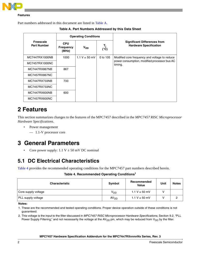
Features
Part numbers addressed in this document are listed in Table A.
2 FeaturesThis section summarizes changes to the features of the MPC7457 described in the MPC7457 RISC Microprocessor Hardware Specifications.
• Power management
— 1.1-V processor core
3 General Parameters• Core power supply: 1.1 V ± 50 mV DC nominal
5.1 DC Electrical CharacteristicsTable 4 provides the recommended operating conditions for the MPC7457 part numbers described herein.
Table A. Part Numbers Addressed by this Data Sheet
FreescalePart Number
Operating Conditions
Significant Differences fromHardware Specification
CPUFrequency
(MHz)VDD
Tj(°C)
MC7447RX1000NB 1000 1.1 V ± 50 mV 0 to 105 Modified core frequency and voltage to reduce power consumption, modified processor bus AC timing.MC7457RX1000NC
MC7447RX867NB 867
MC7457RX867NC
MC7447RX733NB 733
MC7457RX733NC
MC7447RX600NB 600
MC7457RX600NC
Table 4. Recommended Operating Conditions1
Characteristic Symbol Recommended Value
Unit Notes
Core supply voltage VDD 1.1 V ± 50 mV V
PLL supply voltage AVDD 1.1 V ± 50 mV V 2
Notes:1. These are the recommended and tested operating conditions. Proper device operation outside of these conditions is not
guaranteed.
2. This voltage is the input to the filter discussed in MPC7457 RISC Microprocessor Hardware Specifications, Section 9.2, “PLL Power Supply Filtering,” and not necessarily the voltage at the AVDD pin, which may be reduced from VDD by the filter.
MPC7457 Hardware Specification Addendum for the MPC74n7RXnnnnNx Series, Rev. 3
Freescale Semiconductor 3
General Parameters
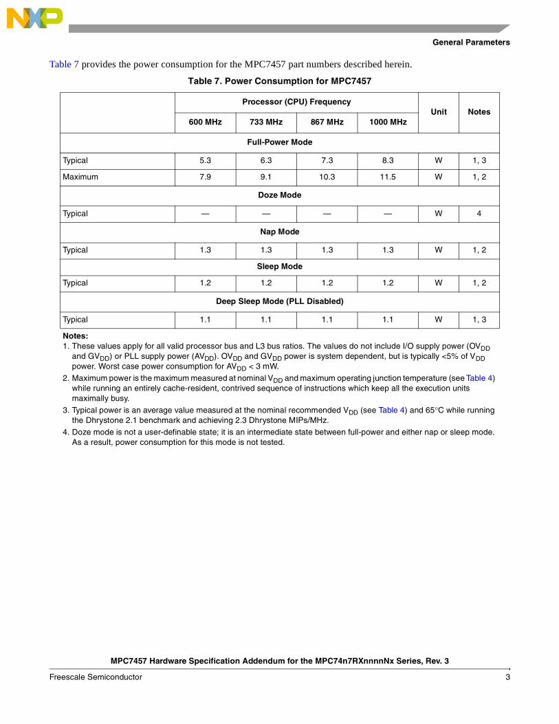
Table 7 provides the power consumption for the MPC7457 part numbers described herein.
Table 7. Power Consumption for MPC7457
Processor (CPU) FrequencyUnit Notes
600 MHz 733 MHz 867 MHz 1000 MHz
Full-Power Mode
Typical 5.3 6.3 7.3 8.3 W 1, 3
Maximum 7.9 9.1 10.3 11.5 W 1, 2
Doze Mode
Typical — — — — W 4
Nap Mode
Typical 1.3 1.3 1.3 1.3 W 1, 2
Sleep Mode
Typical 1.2 1.2 1.2 1.2 W 1, 2
Deep Sleep Mode (PLL Disabled)
Typical 1.1 1.1 1.1 1.1 W 1, 3
Notes: 1. These values apply for all valid processor bus and L3 bus ratios. The values do not include I/O supply power (OVDD
and GVDD) or PLL supply power (AVDD). OVDD and GVDD power is system dependent, but is typically <5% of VDD power. Worst case power consumption for AVDD < 3 mW.
2. Maximum power is the maximum measured at nominal VDD and maximum operating junction temperature (see Table 4) while running an entirely cache-resident, contrived sequence of instructions which keep all the execution units maximally busy.
3. Typical power is an average value measured at the nominal recommended VDD (see Table 4) and 65°C while running the Dhrystone 2.1 benchmark and achieving 2.3 Dhrystone MIPs/MHz.
4. Doze mode is not a user-definable state; it is an intermediate state between full-power and either nap or sleep mode. As a result, power consumption for this mode is not tested.
MPC7457 Hardware Specification Addendum for the MPC74n7RXnnnnNx Series, Rev. 3
4 Freescale Semiconductor
General Parameters
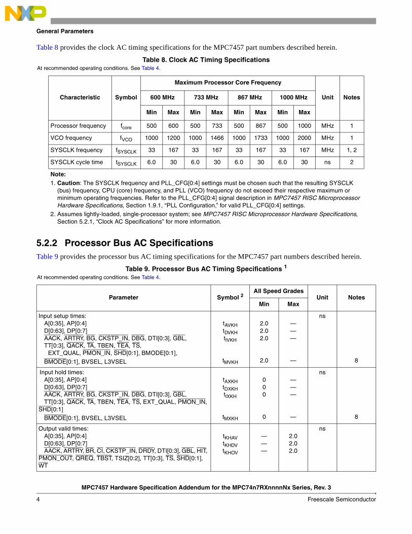
Table 8 provides the clock AC timing specifications for the MPC7457 part numbers described herein.
5.2.2 Processor Bus AC SpecificationsTable 9 provides the processor bus AC timing specifications for the MPC7457 part numbers described herein.
Table 8. Clock AC Timing SpecificationsAt recommended operating conditions. See Table 4.
Characteristic Symbol
Maximum Processor Core Frequency
Unit Notes600 MHz 733 MHz 867 MHz 1000 MHz
Min Max Min Max Min Max Min Max
Processor frequency fcore 500 600 500 733 500 867 500 1000 MHz 1
VCO frequency fVCO 1000 1200 1000 1466 1000 1733 1000 2000 MHz 1
SYSCLK frequency fSYSCLK 33 167 33 167 33 167 33 167 MHz 1, 2
SYSCLK cycle time tSYSCLK 6.0 30 6.0 30 6.0 30 6.0 30 ns 2
Note:1. Caution: The SYSCLK frequency and PLL_CFG[0:4] settings must be chosen such that the resulting SYSCLK
(bus) frequency, CPU (core) frequency, and PLL (VCO) frequency do not exceed their respective maximum or minimum operating frequencies. Refer to the PLL_CFG[0:4] signal description in MPC7457 RISC Microprocessor Hardware Specifications, Section 1.9.1, “PLL Configuration,” for valid PLL_CFG[0:4] settings.
2. Assumes lightly-loaded, single-processor system; see MPC7457 RISC Microprocessor Hardware Specifications, Section 5.2.1, “Clock AC Specifications” for more information.
Table 9. Processor Bus AC Timing Specifications 1
At recommended operating conditions. See Table 4.
Parameter Symbol 2All Speed Grades
Unit NotesMin Max
Input setup times:A[0:35], AP[0:4]D[0:63], DP[0:7]AACK, ARTRY, BG, CKSTP_IN, DBG, DTI[0:3], GBL,TT[0:3], QACK, TA, TBEN, TEA, TS,
EXT_QUAL, PMON_IN, SHD[0:1], BMODE[0:1],
BMODE[0:1], BVSEL, L3VSEL
tAVKHtDVKHtIVKH
tMVKH
2.02.02.0
2.0
———
—
ns
8
Input hold times:A[0:35], AP[0:4]D[0:63], DP[0:7]AACK, ARTRY, BG, CKSTP_IN, DBG, DTI[0:3], GBL,TT[0:3], QACK, TA, TBEN, TEA, TS, EXT_QUAL, PMON_IN,
SHD[0:1]
BMODE[0:1], BVSEL, L3VSEL
tAXKHtDXKHtIXKH
tMXKH
000
0
———
—
ns
8
Output valid times: A[0:35], AP[0:4]D[0:63], DP[0:7]AACK, ARTRY, BR, CI, CKSTP_IN, DRDY, DTI[0:3], GBL, HIT,
PMON_OUT, QREQ, TBST, TSIZ[0:2], TT[0:3], TS, SHD[0:1], WT
tKHAVtKHDVtKHOV
———
2.02.02.0
ns

MPC7457 Hardware Specification Addendum for the MPC74n7RXnnnnNx Series, Rev. 3
Freescale Semiconductor 5
General Parameters
Output hold times:A[0:35], AP[0:4]D[0:63], DP[0:7]AACK, ARTRY, BR, CI, CKSTP_IN, DRDY, DTI[0:3], GBL, HIT,
PMON_OUT, QREQ, TBST, TSIZ[0:2], TT[0:3], TS, SHD[0:1], WT
tKHAXtKHDXtKHOX
0.50.50.5
———
ns
SYSCLK to output enable tKHOE 0.5 — ns
SYSCLK to output high impedance (all except TS, ARTRY, SHD0, SHD1)
tKHOZ — 3.5 ns
SYSCLK to TS high impedance after precharge tKHTSPZ — 1 tSYSCLK 3, 4, 5
Maximum delay to ARTRY/SHD0/SHD1 precharge tKHARP — 1 tSYSCLK 3, 5, 6, 7
SYSCLK to ARTRY/SHD0/SHD1 high impedance after precharge tKHARPZ — 2 tSYSCLK 3, 5, 6, 7
Notes: 1. All input specifications are measured from the midpoint of the signal in question to the midpoint of the rising edge of the input
SYSCLK. All output specifications are measured from the midpoint of the rising edge of SYSCLK to the midpoint of the signal in question. All output timings assume a purely resistive 50-Ω load. Input and output timings are measured at the pin; time-of-flight delays must be added for trace lengths, vias, and connectors in the system.
2. The symbology used for timing specifications herein follows the pattern of t(signal)(state)(reference)(state) for inputs and t(reference)(state)(signal)(state) for outputs. For example, tIVKH symbolizes the time input signals (I) reach the valid state (V) relative to the SYSCLK reference (K) going to the high (H) state or input setup time. And tKHOV symbolizes the time from SYSCLK(K) going high (H) until outputs (O) are valid (V) or output valid time. Input hold time can be read as the time that the input signal (I) went invalid (X) with respect to the rising clock edge (KH) (note the position of the reference and its state for inputs) and output hold time can be read as the time from the rising edge (KH) until the output went invalid (OX).
3. tsysclk is the period of the external clock (SYSCLK) in ns. The numbers given in the table must be multiplied by the period of SYSCLK to compute the actual time duration (in ns) of the parameter in question.
4. According to the bus protocol, TS is driven only by the currently active bus master. It is asserted low then precharged high before returning to high impedance. The nominal precharge width for TS is 0.5 × tSYSCLK, that is, less than the minimum tSYSCLK period, to ensure that another master asserting TS on the following clock will not contend with the precharge. Output valid and output hold timing is tested for the signal asserted. Output valid time is tested for precharge.The high-impedance behavior is guaranteed by design.
5. Guaranteed by design and not tested.
6. According to the bus protocol, ARTRY can be driven by multiple bus masters through the clock period immediately following AACK. Bus contention is not an issue because any master asserting ARTRY will be driving it low. Any master asserting it low in the first clock following AACK will then go to high impedance for one clock before precharging it high during the second cycle after the assertion of AACK. The nominal precharge width for ARTRY is 1.0 tSYSCLK; that is, it should be high impedance before the first opportunity for another master to assert ARTRY. Output valid and output hold timing is tested for the signal asserted.The high-impedance behavior is guaranteed by design.
7. According to the MPX bus protocol, SHD0 and SHD1 can be driven by multiple bus masters beginning the cycle of TS. Timing is the same as ARTRY, that is, the signal is high impedance for a fraction of a cycle, then negated for up to an entire cycle (crossing a bus cycle boundary) before being three-stated again. The nominal precharge width for SHD0 and SHD1 is 1.0 tSYSCLK. The edges of the precharge vary depending on the programmed ratio of core to bus (PLL configurations).
8. BMODE[0:1] and BVSEL are mode select inputs and are sampled before and after HRESET negation. These parameters represent the input setup and hold times for each sample. These values are guaranteed by design and not tested. These inputs must remain stable after the second sample.
Table 9. Processor Bus AC Timing Specifications 1 (continued)At recommended operating conditions. See Table 4.
Parameter Symbol 2All Speed Grades
Unit NotesMin Max
MPC7457 Hardware Specification Addendum for the MPC74n7RXnnnnNx Series, Rev. 3
6 Freescale Semiconductor
Ordering Information
5.2.3 L3 Clock AC SpecificationsThe MPC7457 devices described by this part number specification conform to the L3 clock AC timing specifications provided in the MPC7457 RISC Microprocessor Hardware Specifications. Refer to the hardware specifications for additional information.
5.2.4 L3 Bus AC SpecificationsThe MPC7457 devices described by this part number specification conform to the L3 clock AC timing specifications provided in the MPC7457 RISC Microprocessor Hardware Specifications. Refer to the hardware specifications for additional information.
11 Ordering Information
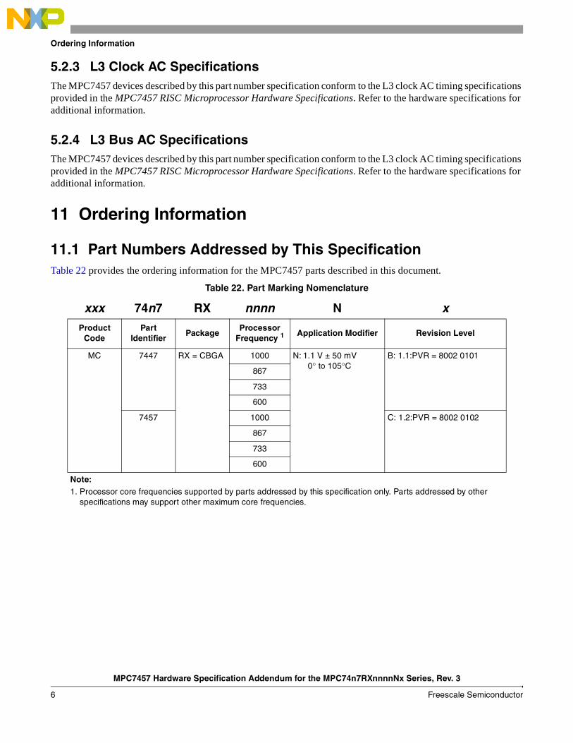
11.1 Part Numbers Addressed by This SpecificationTable 22 provides the ordering information for the MPC7457 parts described in this document.
Table 22. Part Marking Nomenclature
xxx 74n7 RX nnnn N xProduct
CodePart
IdentifierPackage
Processor Frequency 1
Application Modifier Revision Level
MC 7447 RX = CBGA 1000 N: 1.1 V ± 50 mV0° to 105°C
B: 1.1:PVR = 8002 0101
867
733
600
7457 1000 C: 1.2:PVR = 8002 0102
867
733
600
Note: 1. Processor core frequencies supported by parts addressed by this specification only. Parts addressed by other
specifications may support other maximum core frequencies.
MPC7457 Hardware Specification Addendum for the MPC74n7RXnnnnNx Series, Rev. 3
Freescale Semiconductor 7
Ordering Information
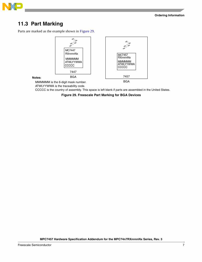
11.3 Part MarkingParts are marked as the example shown in Figure 29.
Figure 29. Freescale Part Marking for BGA Devices
BGANotes:
CCCCC is the country of assembly. This space is left blank if parts are assembled in the United States.
MMMMMM is the 6-digit mask number.ATWLYYWWA is the traceability code.
MC7457RXnnnnNxMMMMMMATWLYYWWA
7457BGA
MC7447RXnnnnNx
MMMMMMATWLYYWWA
7447
CCCCC CCCCC
MPC7457 Hardware Specification Addendum for the MPC74n7RXnnnnNx Series, Rev. 3
8 Freescale Semiconductor
Document Revision History
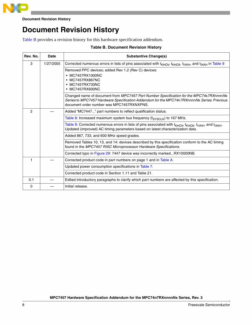
Document Revision HistoryTable B provides a revision history for this hardware specification addendum.
Table B. Document Revision History
Rev. No. Date Substantive Change(s)
3 1/27/2005 Corrected numerous errors in lists of pins associated with tKHOV, tKHOX, tIVKH, and tIXKH in Table 9
Removed PPC devices; added Rev 1.2 (Rev C) devices:
• MC7457RX1000NC • MC7457RX867NC • MC7457RX733NC • MC7457RX600NC
Changed name of document from MPC7457 Part Number Specification for the MPC74x7RXnnnnNx Series to MPC7457 Hardware Specification Addendum for the MPC74n7RXnnnnNx Series. Previous document order number was MPC7457RXNXPNS.
2 — Added “MC7447...” part numbers to reflect qualification status.
Table 8: Increased maximum system bus frequency (fSYSCLK) to 167 MHz.
Table 9: Corrected numerous errors in lists of pins associated with tKHOV, tKHOX, tIVKH, and tIXKH. Updated (improved) AC timing parameters based on latest characterization data.
Added 867, 733, and 600 MHz speed grades.
Removed Tables 10, 13, and 14: devices described by this specification conform to the AC timing found in the MPC7457 RISC Microprocessor Hardware Specifications.
Corrected typo in Figure 29: 7447 device was incorrectly marked...RX10000NB.
1 — Corrected product code in part numbers on page 1 and in Table A.
Updated power consumption specifications in Table 7.
Corrected product code in Section 1.11 and Table 21.
0.1 — Edited introductory paragraphs to clarify which part numbers are affected by this specification.
0 — Initial release.
MPC7457 Hardware Specification Addendum for the MPC74n7RXnnnnNx Series, Rev. 3
Freescale Semiconductor 9
Document Revision History
THIS PAGE INTENTIONALLY LEFT BLANK
MPC7457 Hardware Specification Addendum for the MPC74n7RXnnnnNx Series, Rev. 3
10 Freescale Semiconductor
Document Revision History
THIS PAGE INTENTIONALLY LEFT BLANK

MPC7457 Hardware Specification Addendum for the MPC74n7RXnnnnNx Series, Rev. 3
Freescale Semiconductor 11
Document Revision History
THIS PAGE INTENTIONALLY LEFT BLANK

How to Reach Us:
USA/Europe/Locations Not Listed:Freescale Semiconductor
Literature Distribution CenterP.O. Box 5405, Denver, Colorado 802171-480-768-2130(800) 521-6274
Japan:Freescale Semiconductor Japan Ltd.Technical Information Center3-20-1, Minami-Azabu, Minato-kuTokyo 106-8573, Japan81-3-3440-3569
Asia/Pacific:Freescale Semiconductor Hong Kong Ltd.2 Dai King StreetTai Po Industrial EstateTai Po, N.T. Hong Kong852-26668334
Home Page:www.freescale.com
Information in this document is provided solely to enable system and software implementers to use
Freescale Semiconductor products. There are no express or implied copyright licenses granted
hereunder to design or fabricate any integrated circuits or integrated circuits based on the information
in this document.
Freescale Semiconductor reserves the right to make changes without further notice to any products
herein. Freescale Semiconductor makes no warranty, representation or guarantee regarding the
suitability of its products for any particular purpose, nor does Freescale Semiconductor assume any
liability arising out of the application or use of any product or circuit, and specifically disclaims any
and all liability, including without limitation consequential or incidental damages. “Typical” parameters
which may be provided in Freescale Semiconductor data sheets and/or specifications can and do
vary in different applications and actual performance may vary over time. All operating parameters,
including “Typicals” must be validated for each customer application by customer’s technical experts.
Freescale Semiconductor does not convey any license under its patent rights nor the rights of others.
Freescale Semiconductor products are not designed, intended, or authorized for use as components
in systems intended for surgical implant into the body, or other applications intended to support or
sustain life, or for any other application in which the failure of the Freescale Semiconductor product
could create a situation where personal injury or death may occur. Should Buyer purchase or use
Freescale Semiconductor products for any such unintended or unauthorized application, Buyer shall
indemnify and hold Freescale Semiconductor and its officers, employees, subsidiaries, affiliates, and
distributors harmless against all claims, costs, damages, and expenses, and reasonable attorney
fees arising out of, directly or indirectly, any claim of personal injury or death associated with such
unintended or unauthorized use, even if such claim alleges that Freescale Semiconductor was
negligent regarding the design or manufacture of the part.
Learn More: For more information about Freescale Semiconductor products, please visitwww.freescale.com
MPC7457ECS01ADRev. 301/2005
Freescale™ and the Freescale logo are trademarks of Freescale Semiconductor, Inc. The described product is a PowerPC microprocessor. The PowerPC name is a trademark of IBM Corp. and used under license. All other product or service names are the property of their respective owners.
© Freescale Semiconductor, Inc. 2005.