DESCRIPTION - LabKit · application circuit are optimized for easy PCB layout and cost saving ......
17
Tel: 886-2-66296288 Fax: 886-2-29174598 URL: http://www.princeton.com.tw PT2323 V1.3 - 1 - October, 2005 6-Ch Audio Selector PT2323 DESCRIPTION PT2323 is a 6-Channel Audio Selector utilizing CMOS Technology specially designed for Home Theater System. It provides a built-in 2-Channel to 6-Channel Translator, which can directly mix traditional stereo channel to simulate a 6-Channel audio output. Single power supply (9V), I 2 C Bus Interface as well as very low Total Harmonic Distortion (THD < 0.005%) and other features are incorporated into a single chip thereby providing very high performance. Pin assignments and application circuit are optimized for easy PCB layout and cost saving advantages. FEATURES • Supply Voltage: 9V • 4 Stereo Inputs • One 6-Channel Input • Maximum Input Voltage: 3.75Vrms (1KHz, THD<1%) • Low Total Harmonic Distortion, THD<0.005% (1KHz, 0.2Vrms) • Low Noise: No<4μVrms • I 2 C Bus Interface • Available in 28 Pins, DIP or SOP APPLICATIONS • AV System • Mini Compo • Car Stereo • Multi-Media Audio Systems
Transcript of DESCRIPTION - LabKit · application circuit are optimized for easy PCB layout and cost saving ......

Tel: 886-2-66296288 Fax: 886-2-29174598 URL: http://www.princeton.com.tw
PT2323 V1.3 - 1 - October, 2005
6-Ch Audio Selector PT2323
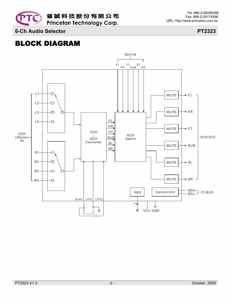
DESCRIPTION PT2323 is a 6-Channel Audio Selector utilizing CMOS Technology specially designed for Home Theater System. It provides a built-in 2-Channel to 6-Channel Translator, which can directly mix traditional stereo channel to simulate a 6-Channel audio output. Single power supply (9V), I2C Bus Interface as well as very low Total Harmonic Distortion (THD < 0.005%) and other features are incorporated into a single chip thereby providing very high performance. Pin assignments and application circuit are optimized for easy PCB layout and cost saving advantages.
FEATURES • Supply Voltage: 9V • 4 Stereo Inputs • One 6-Channel Input • Maximum Input Voltage: 3.75Vrms (1KHz, THD<1%) • Low Total Harmonic Distortion, THD<0.005% (1KHz, 0.2Vrms) • Low Noise: No<4µVrms • I2C Bus Interface • Available in 28 Pins, DIP or SOP
APPLICATIONS • AV System • Mini Compo • Car Stereo • Multi-Media Audio Systems
Tel: 886-2-66296288 Fax: 886-2-29174598 URL: http://www.princeton.com.tw
PT2323 V1.3 - 2 - October, 2005
6-Ch Audio Selector PT2323
BLOCK DIAGRAM
FL
FR
CT
SUB
SL
SR
+
VC C GND
REF Control Unit
FL
FR
CT
SUB
SL
SR
SDASCL I C BUS2
L1
L2
L3
L4
R1
R2
R3
R4
2CH(Stereo)
IN
2CH
6CHConverter
↓ 6CHSwitch
M IXO LP FI LP FO
6CH IN
6CH OUT
FLFR
CTS UB
S LS R
MUTE
MUTE
MUTE
MUTE
MUTE
MUTE
Tel: 886-2-66296288 Fax: 886-2-29174598 URL: http://www.princeton.com.tw
PT2323 V1.3 - 3 - October, 2005
6-Ch Audio Selector PT2323
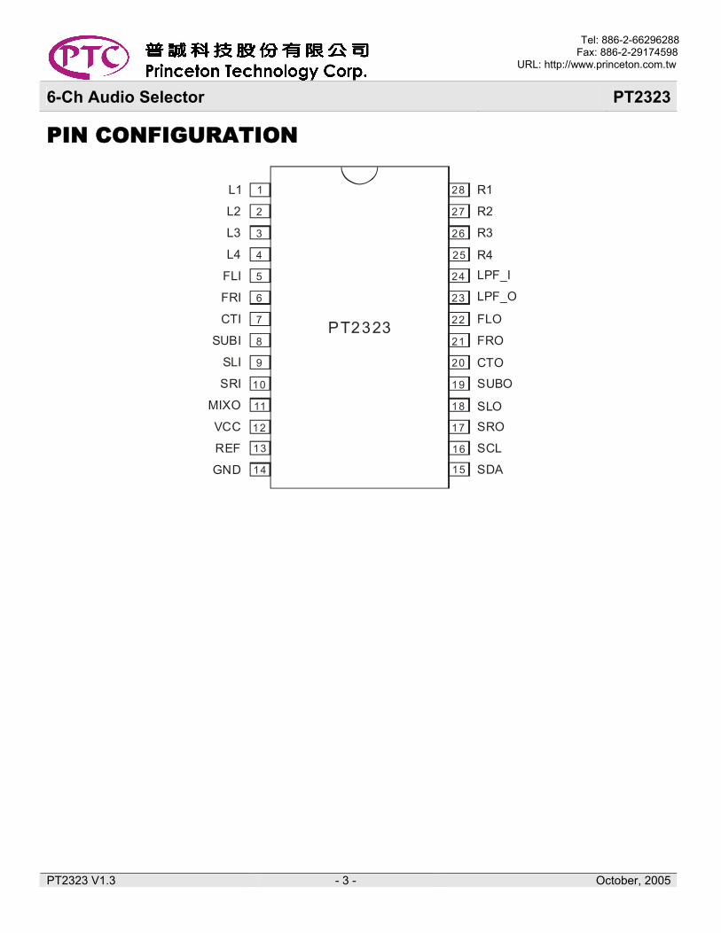
PIN CONFIGURATION
SCL
1
3
2
5
4
8
7
6
10
9
12
11
PT2323
28
26
27
24
25
21
22
23
19
20
17
18
14
13
15 16
L1
L2
L3
L4
FLI
FRI
CTI
SUBI
SLI
SRI
MIXO
VCC
REF
GND SDA
SLO
R1
R2
R3
R4LPF_I
LPF_O
FLO
FRO
CTO
SUBO
SRO
Tel: 886-2-66296288 Fax: 886-2-29174598 URL: http://www.princeton.com.tw
PT2323 V1.3 - 4 - October, 2005
6-Ch Audio Selector PT2323
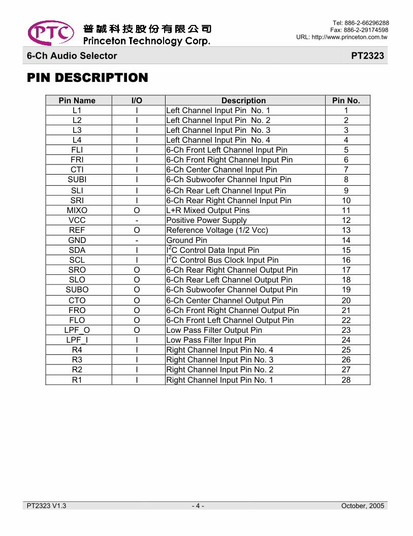
PIN DESCRIPTION
Pin Name I/O Description Pin No. L1 I Left Channel Input Pin No. 1 1 L2 I Left Channel Input Pin No. 2 2 L3 I Left Channel Input Pin No. 3 3 L4 I Left Channel Input Pin No. 4 4 FLI I 6-Ch Front Left Channel Input Pin 5 FRI I 6-Ch Front Right Channel Input Pin 6 CTI I 6-Ch Center Channel Input Pin 7
SUBI I 6-Ch Subwoofer Channel Input Pin 8 SLI I 6-Ch Rear Left Channel Input Pin 9 SRI I 6-Ch Rear Right Channel Input Pin 10
MIXO O L+R Mixed Output Pins 11 VCC - Positive Power Supply 12 REF O Reference Voltage (1/2 Vcc) 13 GND - Ground Pin 14 SDA I I2C Control Data Input Pin 15 SCL I I2C Control Bus Clock Input Pin 16 SRO O 6-Ch Rear Right Channel Output Pin 17 SLO O 6-Ch Rear Left Channel Output Pin 18
SUBO O 6-Ch Subwoofer Channel Output Pin 19 CTO O 6-Ch Center Channel Output Pin 20 FRO O 6-Ch Front Right Channel Output Pin 21 FLO O 6-Ch Front Left Channel Output Pin 22
LPF_O O Low Pass Filter Output Pin 23 LPF_I I Low Pass Filter Input Pin 24
R4 I Right Channel Input Pin No. 4 25 R3 I Right Channel Input Pin No. 3 26 R2 I Right Channel Input Pin No. 2 27 R1 I Right Channel Input Pin No. 1 28

Tel: 886-2-66296288 Fax: 886-2-29174598 URL: http://www.princeton.com.tw
PT2323 V1.3 - 5 - October, 2005
6-Ch Audio Selector PT2323
FUNCTION DESCRIPTION BUS INTERFACE Data are transmitted to and from the microprocessor to the PT2323 via the SDA and SCL. The SDA and SCL make up the BUS Interface. It should be noted that the pull-up resistors must be connected to the positive supply voltage.
DATA VALIDITY A data on the SDA Line is considered valid and stable only when the SCL Signal is in HIGH State. The HIGH and LOW States of the SDA Line can only change when the SCL signal is LOW. Please refer to the figure below.
SD A
SC L
Da ta Lin eS ta b le ,
Da taVa lid
Da ta Chang eAllowed
START AND STOP CONDITIONS A Start Condition is activated when 1. the SCL is set to HIGH and 2. SDA shifts from HIGH to LOW State. The Stop Condition is activated when 1. SCL is set to HIGH and 2. SDA shifts from LOW to HIGH State. Please refer to the timing diagram below.
SD A
SCL
Start Stop
BYTE FORMAT Every byte transmitted to the SDA Line consists of 8 bits. Each byte must be followed by an Acknowledge Bit. The MSB is transmitted first.
Tel: 886-2-66296288 Fax: 886-2-29174598 URL: http://www.princeton.com.tw
PT2323 V1.3 - 6 - October, 2005
6-Ch Audio Selector PT2323
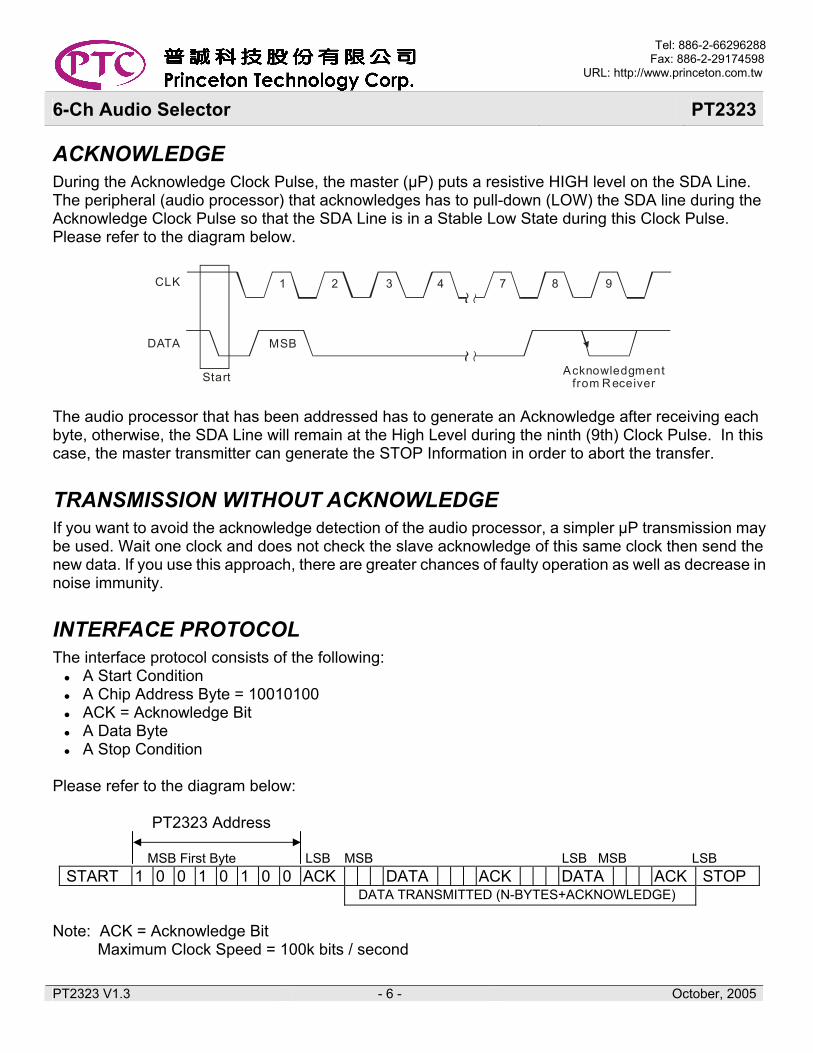
ACKNOWLEDGE During the Acknowledge Clock Pulse, the master (µP) puts a resistive HIGH level on the SDA Line. The peripheral (audio processor) that acknowledges has to pull-down (LOW) the SDA line during the Acknowledge Clock Pulse so that the SDA Line is in a Stable Low State during this Clock Pulse. Please refer to the diagram below.
DATA
CLK
Start
MSB
Acknowledgmentfrom Receiver
1 2 3 7 8 94
The audio processor that has been addressed has to generate an Acknowledge after receiving each byte, otherwise, the SDA Line will remain at the High Level during the ninth (9th) Clock Pulse. In this case, the master transmitter can generate the STOP Information in order to abort the transfer.
TRANSMISSION WITHOUT ACKNOWLEDGE If you want to avoid the acknowledge detection of the audio processor, a simpler µP transmission may be used. Wait one clock and does not check the slave acknowledge of this same clock then send the new data. If you use this approach, there are greater chances of faulty operation as well as decrease in noise immunity.
INTERFACE PROTOCOL The interface protocol consists of the following:
A Start Condition A Chip Address Byte = 10010100 ACK = Acknowledge Bit A Data Byte A Stop Condition
Please refer to the diagram below: PT2323 Address MSB First Byte LSB MSB LSB MSB LSB
START 1 0 0 1 0 1 0 0 ACK DATA ACK DATA ACK STOP DATA TRANSMITTED (N-BYTES+ACKNOWLEDGE)
Note: ACK = Acknowledge Bit Maximum Clock Speed = 100k bits / second

Tel: 886-2-66296288 Fax: 886-2-29174598 URL: http://www.princeton.com.tw
PT2323 V1.3 - 7 - October, 2005
6-Ch Audio Selector PT2323
SOFTWARE SPECIFICATION PT2323 ADDRESS PT2323 Address is shown below.
MSB LSB 1 0 0 1 0 1 0 0
I2C BUS START-UP TIMING After Power is turned ON, PT2323 needs to wait for a short time in order to insure stability. This waiting period is relative to the value of Cref. As the Cref value becomes bigger, the waiting time period for PT2323 to be able to send I2C Bus Signal effectively becomes longer. For example, if Cref = 10µF, after power is turned ON, the waiting time period for PT2323 to send I2C Bus Signal is at least 300 ms. If the waiting time period is less than 300 ms, I2C Control may fail. Please refer to the diagram below.
at least 300ms
POWER ON
VDD
SDA/SCL
V
90% VDD

Tel: 886-2-66296288 Fax: 886-2-29174598 URL: http://www.princeton.com.tw
PT2323 V1.3 - 8 - October, 2005
6-Ch Audio Selector PT2323
Data Bytes MSB LSB Function
1 1 0 0 C3 C2 C1 C0 Input Switch 1 1 1 1 0 0 0 M FL Mute 1 1 1 1 0 0 1 M FR Mute 1 1 1 1 0 1 0 M CT Mute 1 1 1 1 0 1 1 M SUB Mute 1 1 1 1 1 0 0 M SL Mute 1 1 1 1 1 0 1 M SR Mute 1 1 1 1 1 1 1 M All CH Mute
Notes: 1. M = 1 (Mute Function Enabled) 2. M=0 (Mute Function Disabled)
C3 C2 C1 C0 Function 1 0 0 0 Input Stereo Group 4 1 0 0 1 Input Stereo Group 3 1 0 1 0 Input Stereo Group 2 1 0 1 1 Input Stereo Group 1 0 1 1 1 6-Ch Input
Notes: 1. Stereo Group 1 consists of L1 and R1. 2. Stereo Group 2 consist of L2, R2. 3. Stereo Group 3 consists of L3, R3. 4. Stereo Group 4 consists of L4, R4. Add-On Feature
MSB LSB Function 1 1 0 1 0 0 0 0 Enhanced Surround Function Active 1 1 0 1 0 0 0 1 Enhanced Surround Function Disabled 1 0 0 1 0 0 0 0 Mixed Channel (0dB) Setup 1 0 0 1 0 0 0 1 Mixed Channel (+6dB) Setup
2-Ch to 6-Ch Translation PT2323 has a built-in 2-Ch to 6-Ch Translator. Any one of the stereo inputs -- L1/R1, L2/R2, L3/R3, L4/R4 may be selected and converted to a 6-channel output. If the 6-Channel Input is selected, the audio signal just directly flows through the 6-channel output, it is not internally processed by PT2323. During a 2-Ch to 6-Ch translation processes, the original Left and Right signals are also directly outputted and only the Center (CT), Subwoofer (SUB), Rear Right (SR) and the Rear Left (SL) signals are processed by the PT2323. PT2323 provides individual mute functions which prevent output signals from unused stereo input sources from being heard.
Tel: 886-2-66296288 Fax: 886-2-29174598 URL: http://www.princeton.com.tw
PT2323 V1.3 - 9 - October, 2005
6-Ch Audio Selector PT2323
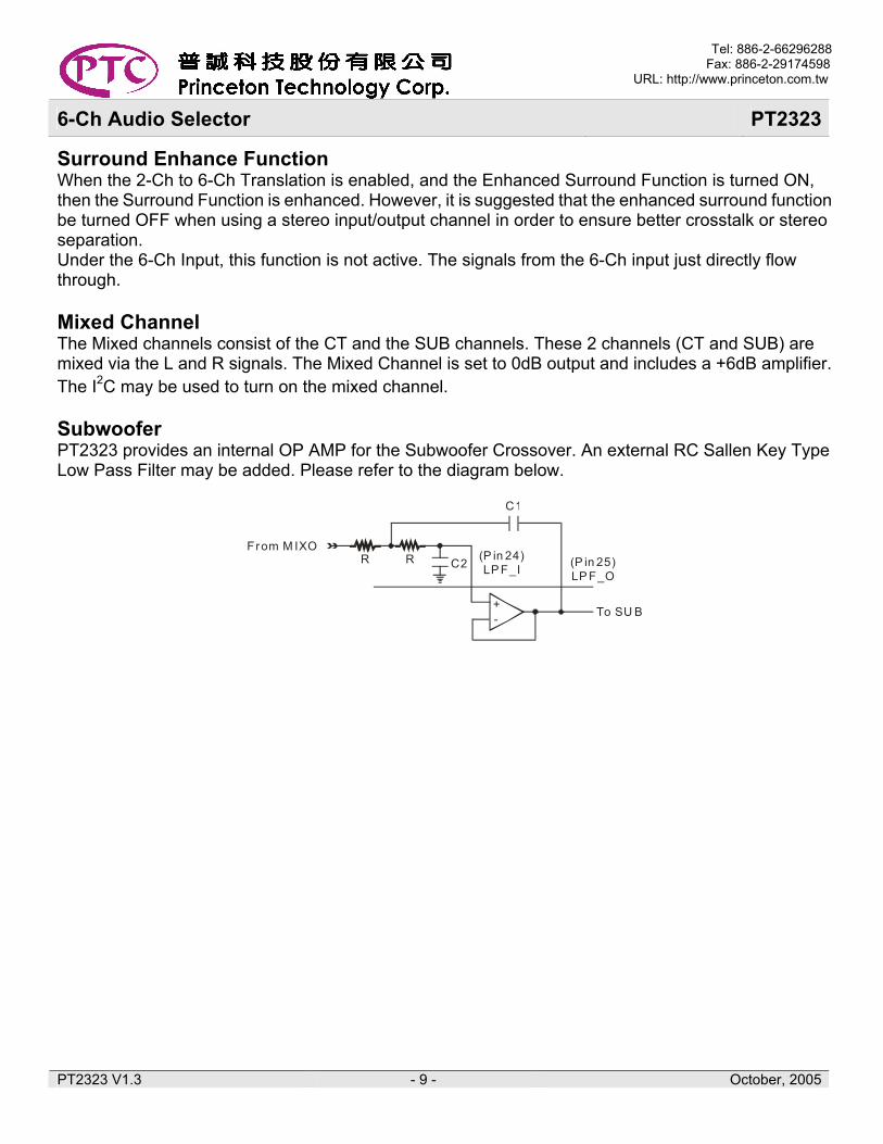
Surround Enhance Function When the 2-Ch to 6-Ch Translation is enabled, and the Enhanced Surround Function is turned ON, then the Surround Function is enhanced. However, it is suggested that the enhanced surround function be turned OFF when using a stereo input/output channel in order to ensure better crosstalk or stereo separation. Under the 6-Ch Input, this function is not active. The signals from the 6-Ch input just directly flow through. Mixed Channel The Mixed channels consist of the CT and the SUB channels. These 2 channels (CT and SUB) are mixed via the L and R signals. The Mixed Channel is set to 0dB output and includes a +6dB amplifier. The I2C may be used to turn on the mixed channel. Subwoofer PT2323 provides an internal OP AMP for the Subwoofer Crossover. An external RC Sallen Key Type Low Pass Filter may be added. Please refer to the diagram below.
(P in 25)LP F_O
To SU B+-
C1
(P in 24)LP F_IC2R R
From M IXO

Tel: 886-2-66296288 Fax: 886-2-29174598 URL: http://www.princeton.com.tw
PT2323 V1.3 - 10 - October, 2005
6-Ch Audio Selector PT2323
Subwoofer Crossover Frequency Response Curve
-50
+5
-45
-40
-35
-30
-25
-20
-15
-10
-5
+0
dBV
20 20k50 100 200 500 1k 2k 5k 10kHz
Note: 1. R=24KΩ (where R is the resistor in the Subwoofer Cross-Over Circuit) 2. : Cross-Over Frequency=280Hz, C1=0.047µf, C2=0.018µf 3. : Cross-Over Frequency=200Hz, C1=0.068µf, C2=0.027µf 4. : Cross-Over Frequency=120Hz, C1=0.1µf, C2=0.047µf 5. C1, C2=Low Pass Filter Capacitor
Tel: 886-2-66296288 Fax: 886-2-29174598 URL: http://www.princeton.com.tw
PT2323 V1.3 - 11 - October, 2005
6-Ch Audio Selector PT2323
ABSOLUTE MAXIMUM RATING Parameter Symbol Rating Unit
Operating Voltage Vs 12 V Operating Temperature Topr -40 ~ 85 Storage Temperature Tstg -65 ~ +150
ELECTRICAL PARAMETERS (Unless otherwise stated:Ta=25, Vcc=9V, RL=100KΩ, f=1KHz)
Parameter Symbol Condition Min. Typ. Max. Unit Supply Voltage VCC 4.5 9 - V Supply Current IS - 4 - mA
Total Harmonic Distortion THD Input=0.2Vrms A-Weighting 0.001 0.005 - %
Output Noise NO RIS=600Ω A-Weighting - 4 - µV
Signal to Noise Ratio SN 0dB=1Vrms A-Weighting - 100 110 dB
Maximum Input Voltage VIMAX RL=50KΩ, 1KHzTHD=1% - 3.75 - Vrms
Voltage Gain GN F=1KHz -1 0 +1 dB Internal Switch Impedance RON - 200 - Ω Cross Talk CT Vin=1Vrms - 90 - dB Channel Separation CS Vin=1Vrms - 90 - dB
Mute Function MUTE Vin=1Vrms A-Weighting - 95 - dB
I2C Bus High Level Input Voltage VIH 0.7VDD - - V I2C Bus Low Level Input Voltage VIL - - 0.3VDD V I2C Bus Initial Time TINIT CREF=10µf - 300 - ms

Tel: 886-2-66296288 Fax: 886-2-29174598 URL: http://www.princeton.com.tw
PT2323 V1.3 - 12 - October, 2005
6-Ch Audio Selector PT2323
APPLICATION CIRCUIT
PT2323
L1
L2
L3
L4
FLI
CTI
SUBI
SLI
SRI
MIXO
VCC
REF
FRI
GND
R1
R2
R3
R4
LPF_I
LPF_O
FLO
FRO
CTO
SUBO
SLO
SRO
SCL
SDA10 Fµ0.147 Fµ
270Ω(NOTE)
270Ω(NOTE)
270Ω(NOTE)
270Ω(NOTE)
270Ω(NOTE)
270Ω(NOTE)
+
I C BUS2
10 Fµ 100K
C2
C1
From MIXO
10 Fµ 100KRch1
Rch2
Rch3
Rch4
10 Fµ100K
Lch1
Lch2
Lch3
Lch4
6CHIN
6CHOUT
<<
<<9V
1
2
3
4
5
6
7
8
9
10
11
12
13
14
28
27
26
25
24
23
22
21
20
19
18
17
16
15
+
+
+
+
+
+
+
+
+
+ +
+
+
+
+
+
+
+
+
+
+
Note: * = An external resistor (R=270Ω) must be connected in series to each of the output pins (FLO, FRO, CTO, SUBO, SLO, SRO) and must be as close as possible to the PT2323 chip.

Tel: 886-2-66296288 Fax: 886-2-29174598 URL: http://www.princeton.com.tw
PT2323 V1.3 - 13 - October, 2005
6-Ch Audio Selector PT2323
ORDER INFORMATION
Valid Part Number Package Type Top Code PT2323 28 Pins, DIP, 600mil PT2323
PT2323-S 28 Pins, SOP, 300mil PT2323-S PT2323 (L) 28 Pins, DIP, 600mil PT2323
PT2323-S (L) 28 Pins, SOP, 300mil PT2323-S Notes: 1. (L), (C) or (S) = Lead Free. 2. The Lead Free mark is put in front of the date code.
Tel: 886-2-66296288 Fax: 886-2-29174598 URL: http://www.princeton.com.tw
PT2323 V1.3 - 14 - October, 2005
6-Ch Audio Selector PT2323
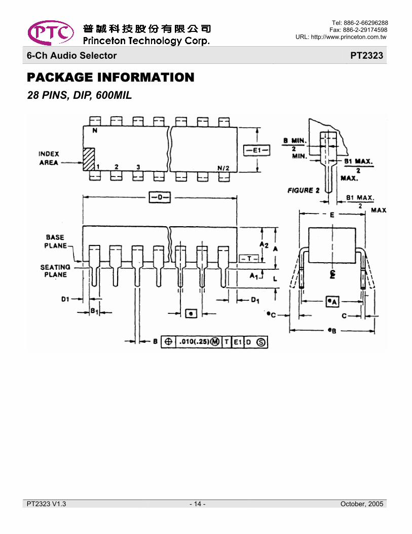
PACKAGE INFORMATION 28 PINS, DIP, 600MIL
Tel: 886-2-66296288 Fax: 886-2-29174598 URL: http://www.princeton.com.tw
PT2323 V1.3 - 15 - October, 2005
6-Ch Audio Selector PT2323
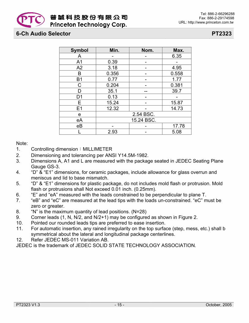
Symbol Min. Nom. Max.
A - - 6.35 A1 0.39 - - A2 3.18 - 4.95 B 0.356 - 0.558
B1 0.77 - 1.77 C 0.204 - 0.381 D 35.1 -- 39.7 D1 0.13 - - E 15.24 - 15.87
E1 12.32 - 14.73 e 2.54 BSC.
eA 15.24 BSC. eB - - 17.78 L 2.93 - 5.08
Note: 1. Controlling dimension:MILLIMETER 2. Dimensioning and tolerancing per ANSI Y14.5M-1982. 3. Dimensions A, A1 and L are measured with the package seated in JEDEC Seating Plane
Gauge GS-3. 4. “D” & “E1” dimensions, for ceramic packages, include allowance for glass overrun and
meniscus and lid to base mismatch. 5. “D” & “E1” dimensions for plastic package, do not includes mold flash or protrusion. Mold
flash or protrusions shall Not exceed 0.01 inch. (0.25mm). 6. “E” and “eA” measured with the leads constrained to be perpendicular to plane T. 7. “eB” and “eC” are measured at the lead tips with the loads un-constrained. “eC” must be
zero or greater. 8. “N” is the maximum quantity of lead positions. (N=28) 9. Corner leads (1, N, N/2, and N/2+1) may be configured as shown in Figure 2. 10. Pointed our rounded leads tips are preferred to ease insertion. 11. For automatic insertion, any rained irregularity on the top surface (step, mess, etc.) shall b
symmetrical about the lateral and longitudinal package centerlines. 12. Refer JEDEC MS-011 Variation AB. JEDEC is the trademark of JEDEC SOLID STATE TECHNOLOGY ASSOCIATION.
Tel: 886-2-66296288 Fax: 886-2-29174598 URL: http://www.princeton.com.tw
PT2323 V1.3 - 16 - October, 2005
6-Ch Audio Selector PT2323
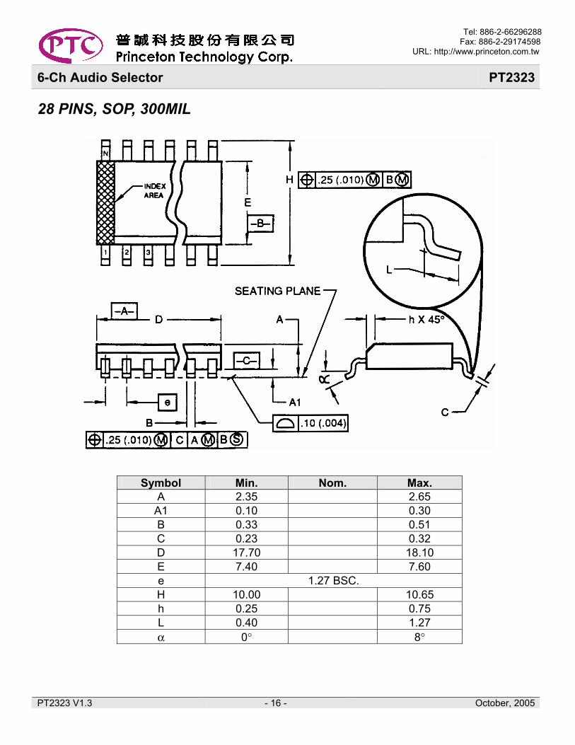
28 PINS, SOP, 300MIL
Symbol Min. Nom. Max. A 2.35 2.65
A1 0.10 0.30 B 0.33 0.51 C 0.23 0.32 D 17.70 18.10 E 7.40 7.60 e 1.27 BSC. H 10.00 10.65 h 0.25 0.75 L 0.40 1.27 α 0° 8°

Tel: 886-2-66296288 Fax: 886-2-29174598 URL: http://www.princeton.com.tw
PT2323 V1.3 - 17 - October, 2005
6-Ch Audio Selector PT2323
Note: 1. Dimensioning and tolerancing per ANSI Y14.5-1982. 2. Dimension “D” does not include mold flash , protrusions or gate burrs. Mold Flash,
protrusion or gate burrs shall not exceed 0.15mm (0.006 in) per side. 3. Dimension “E” does not include interlead flash or protrusions. Interlead flash or
protrusions shall not exceed 0.25 mm (0.010 in) per side. 4. The chamfer on the body is optional. It is not present, a visual index feature must be
located within the crosshatched area. 5. “L” is the length of the terminal for soldering to a substrate. 6. “N” is the number of terminal positions. (N=28) 7. The lead width “B” as measured 0.36 mm (0.014 in) or greater above the seating plane,
shall not exceed a maximum value of 0.61 mm (0.24 in). 8. Controlling dimension: MILLIMETER. 9. Refer to JEDEC MS-013 Variation AE JEDEC is the trademark of JEDEC SOLID STATE TECHNOLOGY ASSOCIATION.