Modular Multilevel inverters
202
ABSTRACT DUTTA, SUMIT. Controls and Applications of the Dual Active Bridge DC to DC Converter for Solid State Transformer Applications and Integration of Multiple Renewable Energy Sources. (Under the direction of Subhashish Bhattacharya). The Dual Active Bridge (DAB) converter was first developed in the University of Wisconsin Madison in 1989. Since then the converter has gained popularity because of its high power density, high efficiency due to ZVS operation under wide load range, bidirectional operation and high frequency isolation. The traditional control of the converter is based on phase shift modulation. The primary bridge which supplies power phase leads the secondary bridge which absorbs power. Extensive research has been done previously on the small signal analysis and the dynamics of the converter. In order to further improve the speed of response of the converter and to have a control on the DC bias level in the high frequency transformer current, a digital predictive current mode controller for the DAB converter is proposed in this thesis. The first chapter discusses the proposed current mode control. The controller is shown to track the reference current within a switching period provided the correct inductance information has been provided to the controller. Additional control methods are developed to observe and remove DC bias flux in the high frequency transformer and the high frequency inductor. Experimental results are provided to verify the working principles of the current controller. In the second portion of the thesis, a multi-terminal topology variant of the DAB converter was explored with storage and renewable energy integration. A multi – limb core transformer based DAB converter (MLC-DAB) is proposed and developed for this application. The equivalent circuit of the MLC-DAB topology is developed using the gyrator concept and the advantage and disadvantage of the proposed topology is shown with respect to a single core multiple winding DAB topology or a series connected multi-terminal DAB topology. A pulse
-
Upload
harikoniki -
Category
Documents
-
view
50 -
download
1
description
Using Modular Multi level inverters for wind generation
Transcript of Modular Multilevel inverters

ABSTRACT
DUTTA, SUMIT. Controls and Applications of the Dual Active Bridge DC to DC Converter
for Solid State Transformer Applications and Integration of Multiple Renewable Energy
Sources. (Under the direction of Subhashish Bhattacharya).
The Dual Active Bridge (DAB) converter was first developed in the University of
Wisconsin Madison in 1989. Since then the converter has gained popularity because of its high
power density, high efficiency due to ZVS operation under wide load range, bidirectional
operation and high frequency isolation. The traditional control of the converter is based on
phase shift modulation. The primary bridge which supplies power phase leads the secondary
bridge which absorbs power. Extensive research has been done previously on the small signal
analysis and the dynamics of the converter. In order to further improve the speed of response
of the converter and to have a control on the DC bias level in the high frequency transformer
current, a digital predictive current mode controller for the DAB converter is proposed in this
thesis. The first chapter discusses the proposed current mode control. The controller is shown
to track the reference current within a switching period provided the correct inductance
information has been provided to the controller. Additional control methods are developed to
observe and remove DC bias flux in the high frequency transformer and the high frequency
inductor. Experimental results are provided to verify the working principles of the current
controller. In the second portion of the thesis, a multi-terminal topology variant of the DAB
converter was explored with storage and renewable energy integration. A multi – limb core
transformer based DAB converter (MLC-DAB) is proposed and developed for this application.
The equivalent circuit of the MLC-DAB topology is developed using the gyrator concept and
the advantage and disadvantage of the proposed topology is shown with respect to a single core
multiple winding DAB topology or a series connected multi-terminal DAB topology. A pulse

width modulation (PWM) based input current control is developed for the MLC-DAB to
integrated different renewable energy sources operating at different maximum power points.
In the final chapter of the thesis the application of the DAB converter in the DC stage of a
Solid State Transformer (SST) is discussed. A single phase cascaded solid state transformer is
considered with the DAB converter in the DC to DC stage. A soft start algorithm is proposed
for the SST to reduce inrush currents at startup. The MLC-DAB topology is considered for the
cascaded single phase SST and is shown to require simpler control compared to a conventional
DAB topology. A micro grid is developed with two parallel connected single phase single
stage SST with MLC-DAB. The system is demonstrated experimentally in grid tied mode with
power being injected into the grid from renewable energy source (emulated by DC source)
integrated to the MLC-DAB stage of the SST. In case of grid failure a black start mode
algorithm is developed and is implemented with one of the SST acting as a master and maintain
the PCC voltage while the slave SST work in constant current injection mode. The critical load
points are recognized within the micro-grid and black start algorithms are developed to provide
for uninterrupted power to the critical load points.

© Copyright 2014 by Sumit Dutta
All Rights Reserved


Controls and Applications of the Dual Active Bridge DC to DC Converter for Solid State
Transformer Applications and Integration of Multiple Renewable Energy Sources
by
Sumit Dutta
A dissertation submitted to the Graduate Faculty of
North Carolina State University
in partial fulfillment of the
requirements for the degree of
Doctor of Philosophy
Electrical Engineering
Raleigh, North Carolina
2014
APPROVED BY:
_______________________________ ______________________________
Subhashish Bhattacharya Iqbal Husain
Committee Chair
________________________________ ________________________________
David Lubkeman Xiangwu Zhang

All rights reserved
INFORMATION TO ALL USERSThe quality of this reproduction is dependent upon the quality of the copy submitted.
In the unlikely event that the author did not send a complete manuscriptand there are missing pages, these will be noted. Also, if material had to be removed,
a note will indicate the deletion.
Microform Edition © ProQuest LLC.All rights reserved. This work is protected against
unauthorized copying under Title 17, United States Code
ProQuest LLC.789 East Eisenhower Parkway
P.O. Box 1346Ann Arbor, MI 48106 - 1346
UMI 3647615Published by ProQuest LLC (2014). Copyright in the Dissertation held by the Author.
UMI Number: 3647615

ii
DEDICATION
To my mother, father and my little brother….

iii
BIOGRAPHY
The author was born in Calcutta (India) on the 31st of January 1984. He did his schooling
from the Ramakrishna Mission Vidyalaya Narendrapur. He finished his bachelor studies from
the Indian Institute of Technology, Kharagpur, India in 2008 from the department of Electrical
Engineering with specialization in Energy Engineering. Since the August of 2008 the author
has been enrolled in the Electrical Engineering Department perusing the Ph.D. in Electrical
Engineering with focus on Power Electronics and Controls.

iv
ACKNOWLEDGMENTS
First of all I would like to thank my Mother and Father and my little Brother for their
unflinching love and support throughout my entire time as a PhD student. I thank my advisor,
Professor Subhashish Bhattacharya for his support and guidance during my PhD. With his
discussions and resourceful ideas I was able to explore several avenues of power electronics
and attain expertise in them. I wish to thank Professor Chandan Chakraborty at IIT Kharagpur
who instilled in me during my undergraduate studies the desire to pursue my doctoral degree
in power electronics. I wish to thank Dr. Sudin Roy who has helped me immensely in my
research with his expert knowledge on Magnetics and Power Converters. I would like to thank
my colleagues Arun Kadavelugu, Sachin Madhusoodanan, Vivek Ramachandaran and Samir
Hazra for the elucidating technical discussions that have been crucial to further my knowledge
in my field of research. I wish to thank Urvir for those Bollywood nights in Cary Crossroads
which I grudgingly went but will miss. I would also like to thank Ansser for being a responsible
and mature roommate at the flag end of my PhD. And finally I completely and thoroughly
thank Aditya, Keyur, Arunesh, Avik and Debadeep in whose sunny and cheerful company I
was able to breathe a little easier during my toughest days so far away from home. I wish to
thank all the members of the FREEDM systems center, past and present for the help and
support though out my stay as a graduate student.

v
TABLE OF CONTENTS
LIST OF TABLES .................................................................................................................. vii
LIST OF FIGURES ............................................................................................................... viii
Chapter 1 Introduction .............................................................................................................. 1
1.1. Research back ground .................................................................................................... 1 1.2. Motivation ...................................................................................................................... 3 1.3. Thesis outline ................................................................................................................. 7 1.4. Research contributions ................................................................................................... 8
Chapter 2 Current Control of Dual Active Bridge Converter ................................................. 10
2.1. Introduction .................................................................................................................. 10
2.2. Motivation for implementing a fast current mode control ........................................... 10 2.3. Peak current mode control ........................................................................................... 12 2.4. Predictive current mode control ................................................................................... 15 2.4.1. Predictive Phase Shift Mode of Control ................................................................... 15 2.4.2. Predictive Half Cycle Phase Shift Mode of Control ................................................. 16 2.4.3. Predictive Full Cycle Phase Shift Mode of Control ................................................. 19
2.5. Duty cycle mode of control ......................................................................................... 23 2.6. Contribution of magnetizing current in the HF DAB transformer .............................. 28
2.6.1. Case 1: Entire Leakage is on primary side ............................................................... 30 2.6.2. Case 2: Entire Leakage is on secondary side ............................................................ 31
2.6.3. Case 3: Distributed Leakage ..................................................................................... 31 2.6.4. Case 4: Duty Cycle mode of control with Flux control ............................................ 34
2.7. Predictive duty cycle mode of control ......................................................................... 36 2.8. Half cycle mode of control .......................................................................................... 37 2.9. Full cycle duty cycle mode of control ......................................................................... 38
2.10. Equal area mode of control ........................................................................................ 43 2.11. Power mode of predictive control .............................................................................. 46
2.12. Experimental verification of predictive control ......................................................... 49 2.13. Conclusions ................................................................................................................ 56
Chapter 3 Multi-terminal application for the Dual Active Bridge converter for multiple
Renewable Energy Source integration .................................................................................... 59
3.1. Introduction .................................................................................................................. 59 3.2. Circulating current in a single limb core topology ...................................................... 60
3.3. Leakage inductance distribution and the impact on the circulating reactive power .... 62 3.4. Coaxial Winding transformer (CWT) based topology ................................................ 63 3.5. Input current control in the CWT based topology ....................................................... 66
3.6. Series connected transformer based topology ............................................................. 67 3.7. Input current control in the series connected topology ................................................ 69 3.8. A multi-limb transformer topology .............................................................................. 71
3.9. Electrical equivalent circuit of the MLC topology ...................................................... 73

vi
3.10. Advantages of the MLC topology based on the copper usage .................................. 77 3.11. Magnetic core material requirement in MLC topology ............................................. 80 3.12. Design of a MLC transformer based on the magnetic stage loss analysis ................. 84
3.12.1. Core loss calculations ....................................................................................................... 88 3.12.2 Copper loss calculations .................................................................................................... 92
3.13. Proximity effect in the windings ................................................................................ 95 3.14. Power flow equations in the MLC topology .............................................................. 97
3.15. A small signal model for the MLC-based DAB converter for analyzing the parameter
sensitivity ............................................................................................................................ 98 3.16.1. Transformer leakage inductor sensitivity analysis for open loop system ....................... 101 3.16.2. Design of a Compensator for improving the variation in stability due to variation in L 103 3.16.3. Evaluation of transfer function sensitivity coefficient: .................................................. 105 3.16.4. Effect of wide variation in input voltage on the converter transfer function .................. 107
3.16. Power smoothing algorithm using energy storage: .................................................. 110 3.17. Experimental results: ............................................................................................... 112 3.18. Conclusions .............................................................................................................. 116
Chapter 4 The solid state transformer application of the Dual Active Bridge converter ..... 118
4.1. Introduction ................................................................................................................ 118 4.2. Single phase SST cascaded topology ......................................................................... 119
4.3. Voltage balance control of the SST ........................................................................... 120 4.4. Inrush current limit at startup ..................................................................................... 126 4.5. Single phase SST topology with the MLC –DAB topology: ..................................... 127
4.6. Experimental results of the single phase SST topology showing the soft start and the
MLC-DAB integration: ..................................................................................................... 130 4.7. The renewable energy hub concept ........................................................................... 133 4.8. Energy management for the renewable energy hub ................................................... 137
4.9. Parallel operation of Single phase SST ...................................................................... 138 4.10. Controller design of the active front end of the SST ............................................... 140 4.11. The single phase PLL .............................................................................................. 142
4.12. Local load management for the single phase SST ................................................... 144 4.13. UPS operation of a single phase SST ...................................................................... 148 4.14. Grid tied parallel operation ...................................................................................... 150 4.15. Black start operation of parallel connected SST in islanded mode ......................... 151 4.16. Critical load placement in SST topology: ................................................................ 157
4.17. Micro grid system stability ...................................................................................... 164 4.18. Black Start Sequence 4 ............................................................................................ 165
4.19. Conclusions .............................................................................................................. 172 Conclusion ............................................................................................................ 174
5.1. Summary of the main results ..................................................................................... 174 5.2. Further scope of future research: ............................................................................... 177
REFERENCES ..................................................................................................................... 179

vii
LIST OF TABLES
Table 3.1: Current and power contributed by each source in the multi-active bridge topology
................................................................................................................................................. 64 Table 3.2: Parameter definition and values required for optimum flux density calculation ... 87
Table 3.3: Peak flux and the number of turns obtained for the central and peripheral limb .. 88 Table 3.4: Steinmetz parameters for the ferrite material “F” (source:
http://fmtt.com/Coreloss2009.pdf) .......................................................................................... 90 Table 3.5: Core volume data for the MLC transformer .......................................................... 90 Table 3.6: Core volume data for the SLC transformer ........................................................... 91
Table 3.7: Core loss data for the MLC and the SLC transformers ......................................... 92
Table 3.8: Table showing the total resistance of the windings for the MLC transformer with
50 turns both on peripheral winding and 50 turns on the central winding ............................. 92
Table 3.9: R.M.S. current through the central and peripheral winding of the MLC-DAB at
rated condition ........................................................................................................................ 94 Table 3.10: Table showing the winding resistance for the series connected core transformer
................................................................................................................................................. 94 Table 3.11: Total loss for a 1 KW system in the MLC and the series connected case ........... 94
Table 3.12: MLC-DAB converter parameters ...................................................................... 100 Table 3.13: Leakage inductance dependence on the system stability ................................... 103 Table 3.14: Table showing the phase margin w.r.t change in L ........................................... 104
Table 3.15: Variation in the phase margin of source to output transfer function with the
variation in source voltage .................................................................................................... 108
Table 3.16: Variation in phase margin for the control to output transfer function ............... 108 Table 4.1: Soft Start algorithm.............................................................................................. 127
Table 4.2: Power modes of operation ................................................................................... 138 Table 4.3: Experimental setup parameters ............................................................................ 142

viii
LIST OF FIGURES
Figure 1.1: Solid State transformer topology ............................................................................ 1 Figure 1.2: The SST topology with the DC micro-grid ............................................................ 2 Figure 1.3: The multi-active bridge topology with grid tied output (Solar panels from CA
Solar) ......................................................................................................................................... 5 Figure 1.4: Different configurations of a multi-port DC-DC topology with a high frequency
accumulator stage as reported in [13]. ...................................................................................... 6 Figure 2.1: Block diagram of the DAB average current controller ........................................ 11 Figure 2.2: Circuit diagram of the DAB converter ................................................................. 12
Figure 2.3: Peak Current Control (switching scheme) for the DAB ....................................... 13
Figure 2.4: Controller for the peak current control. ................................................................ 14 Figure 2.5: Predictive phase shift control ............................................................................... 17
Figure 2.6: Observer loop for the Phase shift Predictive Current Controller ......................... 17 Figure 2.7: Simulation result showing the effect of the observer ........................................... 19 Figure 2.8: The Predictive Full Cycle mode of control implementation diagram .................. 20
Figure 2.9: Stability loss due to inductor value mismatch ...................................................... 22 Figure 2.10: The Duty Cycle mode of control with the timing diagram ................................ 24
Figure 2.11: The Duty Cycle mode of control block diagram ................................................ 25 Figure 2.12: Q vs Time Plot with traditional phase shift mode of control ............................. 26 Figure 2.13: Q vs Time Plot with duty cycle mode of control ............................................... 27
Figure 2.14: Duty cycle control resetting the B-H curve of the Inductor ............................... 27 Figure 2.15: The T-model of the high frequency transformer with the distributed leakage
between the primary and the secondary .................................................................................. 29 Figure 2.16: Equivalent circuit of the High frequency DAB transformer .............................. 30
Figure 2.17: Controller for transformer flux DC level control in case of distributed leakage 33 Figure 2.18: Simulation results for the flux removal algorithm showing the magnetizing
current averaged over one cycle. ............................................................................................ 33 Figure 2.19: Simulation results for the DC flux removal algorithm ....................................... 34
Figure 2.20: Controller for complete DC flux removal .......................................................... 35 Figure 2.21: Simulation results for complete DC flux removal algorithm ............................. 35 Figure 2.22: Experimental results for DC flux removal algorithm ......................................... 36 Figure 2.23: Controller diagram for the half cycle duty cycle mode of control ..................... 38 Figure 2.24: Transient response of the half cycle duty cycle mode of control ....................... 38
Figure 2.25: Timing diagram for the full cycle duty cycle mode of control using down
counters ................................................................................................................................... 40
Figure 2.26: Timing diagram for the full cycle duty cycle mode of control using up-down
counters ................................................................................................................................... 41 Figure 2.27: Simulation result for the full cycle duty cycle mode of control ......................... 42 Figure 2.28: Equal area mode of control ................................................................................ 43 Figure 2.29: Transient response of the equal area mode of control ........................................ 45 Figure 2.30: Equal area mode of control with control point two cycles down the line .......... 46

ix
Figure 2.31: Power Balance in series input parallel output DAB stages ................................ 47 Figure 2.32: Power mode of predictive control ...................................................................... 48 Figure 2.33: Controller block diagram for the power mode of predictive control ................. 49 Figure 2.34: Transient test of the half cycle phase shift current mode control ....................... 50
Figure 2.35: Transient test of the half cycle phase shift current mode control showing the 𝐿𝑅
decay. ...................................................................................................................................... 51 Figure 2.36: Transient test of the half cycle duty cycle current mode control. ...................... 52 Figure 2.37: Transient test of the half cycle duty cycle current mode control along with the
changes in the duty cycles d1 and d2 ....................................................................................... 54
Figure 2.38: Controller diagram for the leakage inductance error compensation .................. 55
Figure 2.39: Transient test of the leakage inductance error compensation............................. 56
Figure 3.1: The Multi-Active Bridge converter concept based on a single limb core topology
................................................................................................................................................. 61 Figure 3.2: Circulating current due to voltage mismatch ....................................................... 61 Figure 3.3: Circulating current due to voltage mismatch in the primaries ............................. 62
Figure 3.4: Multi-terminal CWT based topology as a renewable energy accumulator .......... 65 Figure 3.5: Input current control operation on the CWT based topology ............................... 67
Figure 3.6: The series connected topology ............................................................................. 68 Figure 3.7: The Duty Cycle modulation to implement input current control ......................... 70 Figure 3.8: The MLC based topology ..................................................................................... 72
Figure 3.9: Electrical equivalent of the MLC topology .......................................................... 73 Figure 3.10: A three-limb transformer based topology .......................................................... 74
Figure 3.11: The natural gyrator principle .............................................................................. 74
Figure 3.12: The bond graph model for the three-limb core transformer topology ................ 74
Figure 3.13: Simplified bond graph model ............................................................................. 75 Figure 3.14: Bond graph model with further simplifications ................................................. 75 Figure 3.15: Electrical equivalent of the magnetic stage of the MLC topology ..................... 75
Figure 3.16: Electrical equivalent of the electrical stage of the MLC topology ..................... 76 Figure 3.17: Electrical equivalent of the three limb MLC topology ....................................... 77
Figure 3.18: Flux path in a peripheral and the central winding .............................................. 78 Figure 3.19: Plot of the gain factor w.r.t. the number of limbs .............................................. 80 Figure 3.20: Flux plot for the MLC based topology ............................................................... 82
Figure 3.21: Flux plot for the SLC based topology ................................................................ 82 Figure 3.22: Three-limb MLC and SLC topology .................................................................. 84 Figure 3.23: B-H characteristic of the core material used for the construction of the MLC
topology (source: http://www.mag-inc.com/products/ferrite-cores/f-material) ..................... 85
Figure 3.24: Core loss for the ferrite core material (F) (source: www.mag-
inc.com/products/ferrite-cores/f-material) .............................................................................. 85 Figure 3.25: Core dimensions for the used core 0P49925UC (source: www.mag-inc.com).. 89 Figure 3.26: The waveform showing the voltage and flux plot in the transformer core ........ 90 Figure 3.27: The data sheet for the used Litz wire for the transformer winding (source:
http://www.mwswire.com/pdf_files/mws_tech_book/page16_17_18_19.pdf) ...................... 93

x
Figure 3.28: Top view of the five limb core MLC topology .................................................. 95 Figure 3.29: Electrical equivalent circuit of the MLC topology with the capacitors ............. 96 Figure 3.30: Electrical equivalent circuit of the three limb core topology with two source and
one load ................................................................................................................................... 97
Figure 3.31: Bode plot for the control to output transfer function 𝐺𝑣𝑑𝑠 showing the variation
in phase margin with leakage inductance ............................................................................. 101 Figure 3.32: Compensator designed to compensate for the variation in L ........................... 104 Figure 3.33: Variation of the phase margin and stability of the closed loop system with the
compensator with the variation in the leakage inductance (L) of the transformer. .............. 105
Figure 3.34: Sensitivity coefficient plot for the open loop system (green) and the closed loop
system (blue) showing better attenuation of the sensitivity under closed loop operation .... 107
Figure 3.35: The plot of Gvg w.r.t. changes in the source voltage showing the stable phase
margin ................................................................................................................................... 109 Figure 3.36: Magnitude and phase plot for the variation in control to output transfer function
with the variation in input voltage ........................................................................................ 109
Figure 3.37: Power angle curve for the MLC topology ........................................................ 111 Figure 3.38: Control diagram for the energy management ................................................... 111
Figure 3.39: Energy management algorithm from the power angle perspective .................. 112 Figure 3.40: Lab setup for the MLC topology with the motor generator setup acting as a
wave energy simulator .......................................................................................................... 113
Figure 3.41: Experimental result showing the MLC regulating a DC bus with the wave
energy and battery integrated ................................................................................................ 113
Figure 3.42: The five limb MLC transformer. ...................................................................... 114
Figure 3.43: Terminal voltage waveforms for the five limb MLC transformer ................... 114
Figure 3.44: Control diagram for the input current control operation on the 3 limb MLC
topology ................................................................................................................................ 115 Figure 3.45: Experimental results for the three-limb MLC topology with input current control
............................................................................................................................................... 116 Figure 4.1: Single phase SST topology with cascaded front end and DAB for the DC to DC
stages ..................................................................................................................................... 119 Figure 4.2: Vector Control of the active front end converter ............................................... 120 Figure 4.3: DC voltage balance control for the front end ..................................................... 122
Figure 4.4: Power balance in the DAB stage ........................................................................ 123 Figure 4.5: Simulation results with a voltage sag of 0.6 p.u. with the DC bus regulation intact
............................................................................................................................................... 123 Figure 4.6 Input voltage sag of 0.3 p.u. with the DC bus collapse ....................................... 124
Figure 4.7: A 0.3 p.u. voltage sag with modified DAB power balance control to maintain DC
bus balance ............................................................................................................................ 124 Figure 4.8: Power angle curve for the DAB with different leakage inductors and operating at
different phase shift angles to transfer the same power ........................................................ 125 Figure 4.9: Soft Start of the SST from the auxiliary power supply ...................................... 127 Figure 4.10: Single phase SST with the MLC transformer .................................................. 129

xi
Figure 4.11: The voltage sag simulated with a MLC topology based SST without using any
voltage bus balance control in the DC to DC stage as well as the front end stage ............... 129 Figure 4.12: Experimental setup in the lab ........................................................................... 130 Figure 4.13: Soft start algorithm (DC side waveforms) ....................................................... 131 Figure 4.14: Soft start algorithm (AC side waveforms) ....................................................... 131
Figure 4.15: Steady state operation of the MLC based SST topology .................................. 132 Figure 4.16: Experimental results showing the voltage sag compensation without the voltage
bus balancing control (left). The right shows the startup pf the SST with the inrush current
but without any voltage bus control ...................................................................................... 133 Figure 4.17: The renewable energy hub concept. ................................................................. 134
Figure 4.18: The single phase SST with the DC micro-grid concept. .................................. 134
Figure 4.19: MPPT operation on the renewable energy hub. ............................................... 136 Figure 4.20: Input current control with different current references .................................... 136
Figure 4.21: PWM voltage waveform showing the duty cycle modulation in order to obtain
the current control ................................................................................................................. 137 Figure 4.22: REH with the mode switching operation using the grid as the energy buffer.. 138
Figure 4.23: The parallel connection of two single phase SST ............................................ 139 Figure 4.24: The controller diagram for the d-axes control of the front end. The inner current
loop (above) is shown followed by the outer voltage loop (below) ..................................... 140 Figure 4.25: Controller diagram for the single phase d-q PLL with the all-pass filter for
quadrature voltage vector generation .................................................................................... 143
Figure 4.26: Power flow direction on the single phase SST ................................................. 145 Figure 4.27: Local load management without the RES (left) and with power contribution
from the RES (right) ............................................................................................................. 146 Figure 4.28: Simulation results showing the change in polarity of Id with the RES switched
on and off .............................................................................................................................. 147 Figure 4.29: Experimental results showing the current and voltage waveform of the front end
with and without the RES turned on ..................................................................................... 147 Figure 4.30: The single phase SST as a UPS system with a critical load ............................. 148
Figure 4.31: Flow chart diagram of the black start system for the SST supplying a critical
load ........................................................................................................................................ 149 Figure 4.32: Experimental results of local load shedding during black start upon islanding
from the AC grid. .................................................................................................................. 150 Figure 4.33: Experimental results for the two SST connected in parallel with grid. SST 1 is in
the regenerating mode while SST 2 is in the load mode taking power from the grid .......... 151 Figure 4.34: Flow chart diagram for the black start operation with the slave SST front end
acting as a rectifier under islanded mode .............................................................................. 152 Figure 4.35: Experimental result of the black start of the parallel SST system with the slave
SST front end working as a rectifier. .................................................................................... 153 Figure 4.36: Flow chart sequence diagram of the black start operation of the parallel
connected SST with the master undergoing local load shedding and the slave SST front end
acting as a current controlled inverter ................................................................................... 154

xii
Figure 4.37: Experimental results of the black start operation under load shedding with the
critical load connected to SST 2 (slave DC stage) ................................................................ 155 Figure 4.38: Black start without the feed-forward term on the master SST voltage controller
............................................................................................................................................... 155 Figure 4.39: Experimental results of the black start operation showing the PCC voltage
regulated by the master ......................................................................................................... 156 Figure 4.40: System diagram showing the critical load points ............................................. 158 Figure 4.41: Slave SST showing the reconfigured winding arrangement. ........................... 159 Figure 4.42: Slave SST showing the reconfigured winding arrangement. ........................... 160 Figure 4.43: Black Start sequence (system diagram) ............................................................ 161
Figure 4.44: black start sequence flow chart diagram .......................................................... 162
Figure 4.45: Black Start transient showing the PCC voltage and the line current................ 163 Figure 4.46: Experimental result showing the critical loads being kept undisturbed at the
point of black start ................................................................................................................ 163 Figure 4.47: Equivalent circuit diagram for the micro-grid with sequence 3 and sequence2.
............................................................................................................................................... 164
Figure 4.48: Sequence 4 Black start circuit diagram ............................................................ 166 Figure 4.49: Flow chart diagram for the sequence 4 black start. .......................................... 167
Figure 4.50: Experimental results for the black start sequence 4 ......................................... 168 Figure 4.51: PCC voltage at the instant of black start (sequence 4) ..................................... 169 Figure 4.52: DC stage and front end current wave form after islanding has occurred ......... 170
Figure 4.53: Power flow path in case of 𝑃𝑅𝐸𝑆 >> 𝑃𝑙𝑜𝑎𝑑 .................................................. 171
Figure 4.54: Power flow condition with 𝑃𝑅𝐸𝑆 >> 𝑃𝑙𝑜𝑎𝑑 ................................................. 171

1
Chapter 1 Introduction
1.1. Research back ground
The recent years have seen the growing need of the renewable energy sources (RES)
integrating to the conventional grid. With the development of Power Electronic converters
along and the advancement of power semiconductor devices, RES can now be directly
integrated to the existing grid by means of various power converter topologies. DC to DC
converters provide the interface so that the RES can operate at maximum power point, and DC
to AC inverters are used as an interface to the conventional 60 Hz grid. Amongst the several
topologies that are available for the RES integration the solid state transformer (SST) topology
is becoming widely popular [1], [2] concept. The SST is considered to be a replacement for
the conventional 60 Hz transformer. It has an AC front end followed by an isolated DC to DC
stage followed by inverter supplying a load or another grid (Fig. 1.1).
INPUT
FILTER
INDUCTORAC
DAB stage Output stage
Figure 1.1: Solid State transformer topology

2
The SST unlike a conventional 60 Hz transformer is a multifunctional device. In addition to
providing isolation it provides a DC bus to integrate the renewable energy sources to form a
DC-micro grid [3], [4], [5].
INPUT
FILTER
INDUCTORAC
RES
RES
RES
DC Micro-grid
DAB stage Output stage
Figure 1.2: The SST topology with the DC micro-grid
One of the most popular DC-DC topology for the SST application is the Dual Active bridge
converter (DAB) which is the main topic of discussion in this thesis. The DAB converter was
first developed in 1989 in University of Wisconsin, Madison [6], [7], as an isolated DC to DC
converter for higher power application. Both single phase and three phase topology was
developed. The topology has high-frequency isolation along with bidirectional power flow

3
capability. It is capable of soft switching (ZVS turn on) that reduces the turn on switching
losses. All these properties make the DAB a very suitable candidate for the SST application.
The closed loop control and small signal transfer function of the converter has also been
derived in [6], [8], [9]. The traditional control of the DAB converter is based on phase shift
modulation where the leading bridge provides power to the lagging bridge. A dual loop control
for the DAB has been proposed in [9]. Both the outer (voltage) and the inner (current) control
loop are based in PI regulators with the assumption that the inner loop is faster than the outer
loop by a factor of 10. This decouples the outer voltage and inner current loop but a bandwidth
limit on the outer voltage control loop. To improve the outer voltage bandwidth, the inner
current loop bandwidth needs to be improved which can be achieved by implementing a
predictive current mode control. However in literature the predictive current mode control for
the DAB has not been reported.
1.2. Motivation
Considering the DAB converter having a dual loop control, in order to improve the
bandwidth of the outer voltage loop the inner current loop has to be made fast. This provides
the motivation of developing a predictive current control as the inner current loop for the DAB
converter. The predictive current control proposed in [10] has the advantage of providing a
response within one switching cycle, thus having a bandwidth equal to the switching
frequency. This allows the outer voltage loop to have a higher bandwidth of operation and thus
provide for a faster response. Furthermore the inner current loop based on average current
measurement [1] requires continuous sampling over one switching cycle or half cycle. The

4
predictive current mode control on the other hand requires sampling only once or twice in the
switching cycle that reduces burden on the controller. This provides the motivation for
investigating the predictive current mode control for the DAB converter. The renewable energy
integration however provides a different challenge for the DAB converter. (Fig. 1.2). Parallel
connection of several different renewable energy sources requires either master-slave mode of
control or parallel DC droop mode of control [11]. The complexity in controls provides the
motivation of integrating the RES directly within the DAB magnetic stage. This leads to a
multi-terminal DAB stage design where different terminals are connected to different RES.
The quad – active bridge (QAD) converter has been proposed [4] where multiple input bridges
are connected to a RES and the output bridge is load connected or grid tied. Fig. 1.3, the multi-
active bridge topology, the windings connected to each RES cuts the same flux. Hence they
get the same induced voltage across each winding. Mismatch in the winding voltages with the
source voltage will lead to circulating reactive current flowing through the converter bridges
[22] leading to higher losses and lower efficiency. Further topologies in the multiport DAB
have been reported in [4], [13] (Fig. 1.4). Thus in case there is wide voltage variation between
the different renewable sources, there is a requirement for decoupling the different sources
from each other. The problem of cross coupling between the renewable energy sources have
been dealt with in [4]. However a topology based solution was never considered to decouple
the individual RES from each other while still maintaining galvanic isolation.

5
Multi-Active Bridge Output stage
Renewable Energy
Sources (Solar)
Grid
Battery/Storage
Figure 1.3: The multi-active bridge topology with grid tied output (Solar panels from CA
Solar)
This led to the search for an alternate topology to integrate multiple RES while decoupling
each source from the other. The concept of flux accumulation was considered and instead of a
single limb core, a multi-limb approach was developed and the windings, instead of linking to
a single common core, were linked to separate limbs to decouple individual sources from each
other.

6
Renewable
Source
Renewable
Source
Grid
Load
Renewable
Source
Grid
Load
Renewable
Source
Renewable
Source
Grid
High Frequency Accumulator
RES
Figure 1.4: Different configurations of a multi-port DC-DC topology with a high frequency
accumulator stage as reported in [13].

7
1.3. Thesis outline
Chapter 2 discusses the predictive current mode control for the DAB converter. Based
on the different sampling points of the switching cycle, there can be different predictive current
controllers. The different current controllers have been discussed in details with simulation
results. Experimental verification of the controller has also been shown with step change in the
current response to show that as the reference changes, the controller is capable to track the
change in one switching cycle. Since the controller is heavily dependent on the leakage
inductance value, a compensation loop was also proposed to remove the error due to leakage
inductance mismatch. The compensation algorithm has also been verified through
experimental results.
Chapter 3 proposes the multi-terminal DAB converter for multiple renewable energy
source integration. The problem of circulating reactive power has been addressed by
implementing a multi-limb core transformer for the DAB (MLC-DAB) that acts as an energy
accumulator. Power flow control was demonstrated with power smoothening using battery as
an energy buffer. Input current control was also implemented and demonstrated with
experimental verification showing the ability of the converter to do maximum power point
tracking.
Chapter 4 demonstrates the application of the developed MLC- DAB from Chapter 3 for
grid integration of renewable energy sources. A single phase solid state transformer topology
was considered with a cascaded front end with three DC bus. The MLC-DAB was integrated

8
into the DC stage of the SST showing simpler control on the front end as well as the DC bus.
A parallel MLC-SST test bed was developed and the system was islanded to form a micro-grid
with two parallel SST. Power sharing was demonstrated under islanding condition with master-
slave mode of control.
1.4. Research contributions
The following are the research contributions from the dissertation:
1. A duty cycle mode of control was developed for the Dual Active Bridge converter.
2. A phase shift based predictive current mode control was developed for the Dual Active
Bridge Converter.
3. A duty cycle based predictive current mode control was developed for the Dual Active
Bridge Converter.
4. A stability analysis was performed to show the dependence of the phase shift mode
predictive controller on the leakage inductance value and the stability limit have been
reported.
5. A compensation algorithm was developed to compensate for the L-variation in the
controller.
6. A multi - limb –core based Dual Active Bridge converter (MLC-DAB) was proposed
with multiple input and single output for integrating multiple renewable energy sources
to the converter.

9
7. Equivalent circuit for the 3 – limb core and 5 – limb core based multi-limb transformer
was developed using the gyrator principle.
8. A PWM based input current control algorithm was developed to separately control the
source currents of different sources connected to the MLC-DAB converter.
9. An alternate DC - DC converter topology for the DC stage of the cascaded solid state
transformer was proposed based on the multi-limb transformer topology (MLC-DAB
based SST) and the advantages in the control applications were shown.
10. A renewable energy hub concept was proposed to integrate multiple renewable energy
sources to the grid based on the MLC-DAB concept.
11. A black start sequence was developed for parallel MLC-DAB based SST operation
during islanding using the Master slave mode of power sharing.

10
Chapter 2 Current Control of Dual Active Bridge Converter
2.1. Introduction
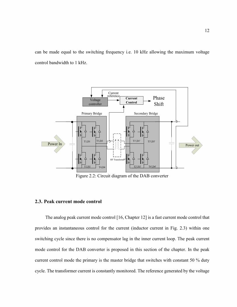
The Dual Active Bridge (DAB) converter (Fig. 2.2) has two H-Bridges (primary and
secondary) that are switched at 50% duty cycle. Power flow is controlled from one bridge to
another by phase shift modulation [6]. A duty cycle modulation for the DAB converter to
increase the ZVS range under light load condition have been reported [14], [15], [48]. However
no research has been done on implementing a fast predictive current mode control. Nor has
there been any research on removing the DC bias in the high frequency transformer currents
under load transients or steady state. The first section of this chapter provides the motivation
of implementing a fast inner current loop along with the outer voltage loop. An analog based
peak current controller is also proposed in the following section. Next the digital predictive
current controller is proposed based on the phase shift approach. A duty cycle mode of control
is proposed that is implemented to remove the DC bias in the transformer current. Finally a
power based controller is proposed that allows parallel operation of the converters with power
balancing. The proposed controllers are verified with simulation platform (MATLAB
Simulink) and experimental results.
2.2. Motivation for implementing a fast current mode control
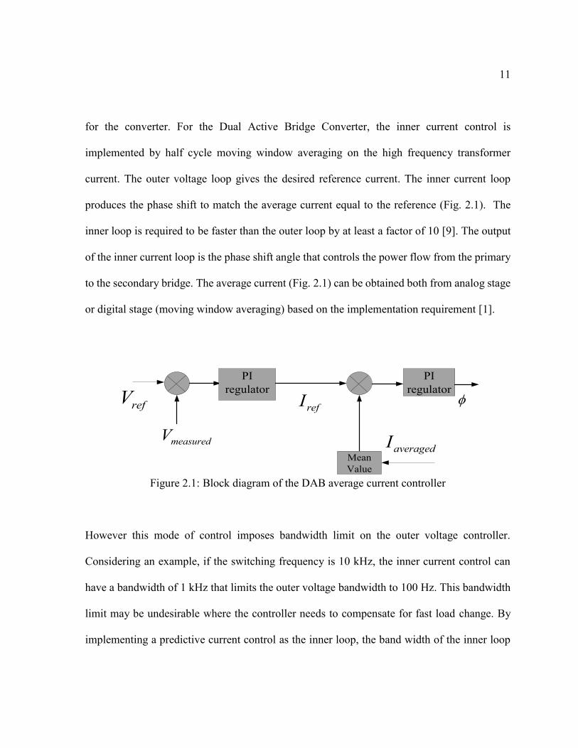
A dual loop control (outer voltage loop with inner current loop) is the most popular
method for controlling any DC to DC or DC to AC converter since it provides a current limit
11
for the converter. For the Dual Active Bridge Converter, the inner current control is
implemented by half cycle moving window averaging on the high frequency transformer
current. The outer voltage loop gives the desired reference current. The inner current loop
produces the phase shift to match the average current equal to the reference (Fig. 2.1). The
inner loop is required to be faster than the outer loop by at least a factor of 10 [9]. The output
of the inner current loop is the phase shift angle that controls the power flow from the primary
to the secondary bridge. The average current (Fig. 2.1) can be obtained both from analog stage
or digital stage (moving window averaging) based on the implementation requirement [1].
PI
regulator
PI
regulator
refV
measuredV
refI
averagedIMean
Value
Figure 2.1: Block diagram of the DAB average current controller
However this mode of control imposes bandwidth limit on the outer voltage controller.
Considering an example, if the switching frequency is 10 kHz, the inner current control can
have a bandwidth of 1 kHz that limits the outer voltage bandwidth to 100 Hz. This bandwidth
limit may be undesirable where the controller needs to compensate for fast load change. By
implementing a predictive current control as the inner loop, the band width of the inner loop
12
can be made equal to the switching frequency i.e. 10 kHz allowing the maximum voltage
control bandwidth to 1 kHz.
Voltage
controller
Current
Control
Phase
Shift
Current reference
Primary Bridge Secondary Bridge
Power In Power out
HF Transformer
T1,D1
T2,D2
T3,D3
T4,D4 T4',D4'T2',D2'
T1',D1' T3',D3'
Figure 2.2: Circuit diagram of the DAB converter
2.3. Peak current mode control
The analog peak current mode control [16, Chapter 12] is a fast current mode control that
provides an instantaneous control for the current (inductor current in Fig. 2.3) within one
switching cycle since there is no compensator lag in the inner current loop. The peak current
mode control for the DAB converter is proposed in this section of the chapter. In the peak
current control mode the primary is the master bridge that switches with constant 50 % duty
cycle. The transformer current is constantly monitored. The reference generated by the voltage

13
loop I0 is compared with the measured value Itransformer (Fig. 2.3 & Fig. 2.4) the switching
scheme for the control is shown in Fig. 2.3. The switching is realized using an S R flip flop.
There is no phase shift as such unlike average mode of control. Power flow is hence controlled
by the current reference generated by the voltage controller. Although the name of the
controller is peak current mode control, it is really not the peak current that is being monitored.
The reference current can be used to regulate the current at ωt = φ or the current at ωt = π
using different switching schemes. The switching scheme to regulate the current at ωt = φ has
been discussed.
Figure 2.3: Peak Current Control (switching scheme) for the DAB
14
Vref
PIIref
Iref >=
-Iref <=
Q
!Q
S
R
S1
S2
S3
S4
S5
S6
S7
S8
Master Unit
Primary
Bridge
Slave unit
Secondary Unit
Vmeasured
Fixed frequency pulses 50%
duty cycle
rtransformeI
Figure 2.4: Controller for the peak current control.
The current I0 at ωt = φ that is set to follow the desired reference can be related to the input
voltage Vin and output voltage Vout as per (2.1).
𝐼0 = − 𝑉𝑖𝑛
𝜔𝐿(𝑑𝜑 +
𝜋
2 (1 − 𝑑)) , 𝑑 =
𝑉𝑜𝑢𝑡
𝑉𝑖𝑛, 𝜔 = 2𝜋𝐹𝑠𝑤𝑖𝑡𝑐ℎ𝑖𝑛𝑔 (2.1)
𝐹𝑠𝑤𝑖𝑡𝑐ℎ𝑖𝑛𝑔 is the switching frequency of the converter, L is the leakage inductance of the
transformer and 𝜑 is the phase shift angle between the primary and the secondary bridge. Thus

15
for a perticular d the current I0 becomes fixed that drives the set and reset points on the SR flip
flop of the peak current control. This control is fast and takes place within one switching cycle
of the of the converter. However the disadvantage is that continuous sampling is demanded
and has to take place in analog domain. A digital implementation of this controller is difficut
which provides the motivation for the predictive current mode of control where the sampling
can take place once or twice within one cycle and the control implementation can be done
based on those sampled values only.
2.4. Predictive current mode control
The predictive current mode control [10] works by predicting the next state control
parameter (phase shift or duty cycle) based on the previous state values. The predictive control
mode for the DAB converter based on the phase shift is discussed in the following section.
2.4.1. Predictive Phase Shift Mode of Control
The predictive phase shift control for the DAB is discussed in this section. The current is
sampled once in every switching cycle and the phase shift angle is calculated and updated at
the beginning of the next cycle. Based on the number of times the current is sampled in the
cycle and update takes place and the calculations are done, the predictive phase shift mode of
control can be classified as follows:
1) Half cycle mode of control
2) Full cycle mode of control

16
Both the methods have their own respective advantages and disadvantages from the control
and parameter sensitivity point of view. The following sections discuss the two controllers in
details.
2.4.2. Predictive Half Cycle Phase Shift Mode of Control
In this mode of control the current is sampled at θ = 0 and the current at ωt = π (or ωt =
φ) is the reference current and they are related as shown in Fig. 2.5 and Fig. 2.6. The required
phase shift angle is pre-calculated from the equations shown in (2.2a) or (2.2b) and updated at
the beginning of each switching cycle. The disadvantage of this mode of control is the sampled
point θ = 0 and the reference point ωt = π (or ωt = φ) are not the same (Fig. 2.5). Hence we
might need an added loop that observes the reference point. This observer model can also serve
as a control loop to reduce parameter sensitivity of the controller. A mismatch between the
desired reference and the actual reference might occur of there is an error in the inductor value
that has been fed to the controller. Under such circumstance the error will be carried over in
the phase angle calculation without the controller knowing. Fig. 2.6 explains the idea behind
the installation of the observer. In this particular case the predictive controller samples the
current at ωt = 0 and the reference current is at ωt = φ. If the current is sampled at ωt = 0 and
the current at ωt = φ is considered as the reference then the sampled current I0 is related to the
reference current Iref as follows in (2.2a)
𝐼𝑟𝑒𝑓 = 𝐼𝜔𝑡=𝜑 = 𝐼0 +𝑉𝑖𝑛 + 𝑉𝑜𝑢𝑡𝜔𝐿
𝜑 (2.2𝑎)
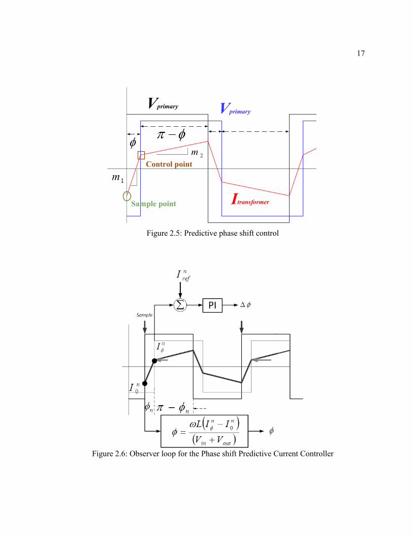
17
Itransformer
Vprimary Vprimary
Sample point
Control point
Figure 2.5: Predictive phase shift control
Figure 2.6: Observer loop for the Phase shift Predictive Current Controller

18
Keeping the sampling point same if the current is referred at ωt = π the equation becomes as
follows in (2.2b)
𝐼𝑟𝑒𝑓 = 𝐼𝜔𝑡=𝜋 = 𝐼0 +𝑉𝑖𝑛 + 𝑉𝑜𝑢𝑡𝜔𝐿
𝜑 +𝑉𝑖𝑛 − 𝑉𝑜𝑢𝑡𝜔𝐿
(𝜋 − 𝜑) (2.2𝑏)
From either (2.2a) or (2.2b) the phase shift angle can be calculated in a deadbeat fashion. The
phase angle updates within one cycle and does not depend on the previous state value. However
since the sampled point is not observed, the predictive equation is heavily dependent on the
accuracy of the measured leakage inductor value. In order to make the controller insensitive
additional observer is introduced as shown in Fig. 2.6. The observer samples the current at the
referring points on the switching cycle, at ωt = φ in the case of Fig. 2.6. Since this is the
reference current, a proportion-integral control loop is implemented that adds an error phase
angle to the predicted phase to compensate for the error (Fig. 2.6). Fig. 2.7 shows the
simulation results with the observer in place. An error was intentionally inserted in the inductor
value in the controller. Lactual was 100 μH while Lcontroller was 150 μH. The green in the figure
is the reference current coming from the controller while red was the real reference current
generated by the predictive law in (2.2a). We see that the control action generated by the
installed observer actually brings back the sampled current to the reference current.

19
Figure 2.7: Simulation result showing the effect of the observer
2.4.3. Predictive Full Cycle Phase Shift Mode of Control
In this mode the sampled current and the referenced current occur at the same point. The
controller samples the current at the mid-point of the half cycle i.e. at ωt = π/2 (Fig. 2.8). This
sampling mode is adopted since sampling at the beginning (ωt = 0) or middle of the cycle (ωt
= π) means sampling at a switching instant. The current sensor may pick up the switching noise
and that might lead to erroneous control action. Hence the current is sampled and held in the
ADC register at the middle of the half cycle or when the up-down counter in the DSP reaches
the count value N (Fig. 2.8). There is no switching action at this instant. Interrupt is generated
at the instant when the counter reaches N/2 on down count. All the control calculations are
done at that point. Once the new phase shift value is calculated from old value and the error,

20
the new value is loaded phase shift resistor and the effect takes place at the beginning of the
next counter period when the counter starts counting up from zero. The next state phase shift
angle φn+1 can be related to φn as per (2.3).
𝜑𝑛+1 = 𝜑𝑛 +(𝐼𝑛+1 − 𝐼𝑛)𝜔𝐿
∆𝑉1 − ∆𝑉2, 𝑤ℎ𝑒𝑟𝑒 𝐼𝑛+1 = 𝐼𝑟𝑒𝑓 (2.3)
The principle advantage of this mode of control is that the sampled current and the reference
current occur at the same point in the switching cycle. Hence an additional observer is not
required. In case of inductance mismatch the system is convergent.
N
2N
2N
1. ADC
Samples
2. Interrupt for
control
calculation
3. New
parameters
loaded
One Switching
cycle
n 1n
nI 1nI
n 1 n
DS
P C
OU
NT
ER
DA
B V
OL
TS
AN
D
CU
RR
EN
TS
Figure 2.8: The Predictive Full Cycle mode of control implementation diagram

21
It can be mathematically proven that in the event that there is an error in the leakage inductance
measurement and if that error is within a particular bound, the actual current will converge to
the reference current within several cycles. The proof is as follows:
𝑖𝑛+1 = 𝑖𝑛 +∆𝑉2𝜔𝐿
𝜋
4−∆𝑉1𝜔𝐿
𝜑𝑛 −∆𝑉2𝜔𝐿
(𝜋 − 𝜑𝑛+1) +∆𝑉1𝜔𝐿𝜑𝑛+1 +
∆𝑉2𝜔𝐿
(𝜋
4− 𝜑𝑛+1) (2.4)
Where ∆𝑉1 = 𝑉𝑖𝑛 + 𝑉𝑜𝑢𝑡 and ∆𝑉2 = 𝑉𝑖𝑛 − 𝑉𝑜𝑢𝑡. Substituting 3 in 4 we get:
𝑖𝑛+1 = 𝐼𝑟𝑒𝑓 (𝐿𝑑𝑠𝑝
𝐿𝑎𝑐𝑡) + 𝐼𝑛 (1 −
𝐿𝑑𝑠𝑝
𝐿𝑎𝑐𝑡) = 𝐼𝑟𝑒𝑓 (
𝐿
𝐿 + ∆𝐿) + 𝐼𝑛 (
∆𝐿
𝐿 + ∆𝐿) (2.5)
Here 𝐿𝑑𝑠𝑝 = 𝐿 and 𝐿𝑎𝑐𝑡 = 𝐿 + ∆𝐿.
∴ 𝑖𝑛+2 = 𝐼𝑟𝑒𝑓 (𝐿
𝐿 + ∆𝐿) (1 +
∆𝐿
𝐿 + ∆𝐿) + 𝐼𝑛 (
∆𝐿
𝐿 + ∆𝐿)2
∴ 𝑖𝑛+3 = 𝐼𝑟𝑒𝑓 (𝐿
𝐿 + ∆𝐿) [1 +
∆𝐿
𝐿 + ∆𝐿+
∆𝐿
𝐿 + ∆𝐿2
] + 𝐼𝑛 (∆𝐿
𝐿 + ∆𝐿)3
∴ lim𝑘→∞
𝑖𝑛+𝑘 = 𝐼
= 𝐼𝑟𝑒𝑓 (𝐿
𝐿 + ∆𝐿) lim𝑘→∞
[1 +∆𝐿
𝐿 + ∆𝐿+⋯
∆𝐿
𝐿 + ∆𝐿𝑘−1
]
+ 𝐼𝑛 (∆𝐿
𝐿 + ∆𝐿)𝑘
(2.6)
∴ 𝐼 = 𝐼𝑟𝑒𝑓 (𝐿
𝐿 + ∆𝐿)
1
1 −∆𝐿
𝐿 + ∆𝐿
= 𝐼𝑟𝑒𝑓 , 𝑠𝑖𝑛𝑐𝑒 lim𝑘→∞
(∆𝐿
𝐿 + ∆𝐿)𝑘
≈ 0

22
The above proof shows that if the measured value of the inductor Ldsp is offset from the actual
value of the inductance Lact by a margin of ΔL there is convergence in the geometric
progression (2.6) as long as ∆L ≤ L and the sampled current will converge to the reference
current within several cycles. The simulation result in Fig. 2.9 shows the operation of the
controller with gradually increasing ∆L. The Lact was 100 μH. In the figure when ∆L < L the
converter is stable and the sampled current tracks the reference current. But when ∆L = L
occurs the current goes out of bound making the system unstable.
Figure 2.9: Stability loss due to inductor value mismatch
In the next section of the paper an alternate duty cycle mode of switching is shown for the
DAB converter. The primary switches are still switched at 50 % duty cycle but the secondary

23
switches are duty cycle modulated. There are several advantages of that method of modulation.
The normal proportional-integral based controller in duty cycle mode is discussed first
followed by the predictive duty cycle based control.
2.5. Duty cycle mode of control
A PWM based duty cycle mode of control has already been established to increase the
ZVS range under light load conditions. The motivation behind the duty cycle mode of control
proposed here is to remove the unwanted DC bias in the high frequency inductor of the DAB
that might lead to saturation [17]. The duty cycle mode of control proposes an alternate
switching strategy on the secondary side of the DAB converter [41], [42]. The primary side is
switched to 50% of the period. The secondary side switches are switched independently using
duty cycle modulation. The duty cycle switching strategy is described in Fig. 2.10. Switches
(S6, S7) and (S5, S8) of the secondary bridge are required to be turned on for the period shown
in the timing diagram. When the diode is conducting at the beginning of the switching period
(S6 & S7) are turned on. After the required duty period that switches are forced turned off
forcing the diodes (D5 and D8) to take over. The gate pulse for the switches (S6, S7) is given
by the red pulse while that of switches (S5, S8) is given by the dotted blue pulse. The duty cycle
for the switches is less than one quarter of the entire switching period (π⁄2). The switches on
the secondary side can be cross switched since (S6 & S7) share the same pulse while (S5 & S8)
share the same pulse. In the dead-time where no switches are turned on the diodes (D5, D8) &
(D6, D7) keep the current flowing. This control is possible since the secondary bridge is lagging
in nature. This mode of control makes the duty cycle for the switches (S6, S7) and (S5, S8)

24
independent of each other. By changing one duty with respect to the other it is possible to apply
positive volts seconds or negative volt seconds across the DAB inductor terminals and force a
DC bias in the high frequency AC current. In other words if there is a DC bias already in the
current, it is possible to remove it by selecting the duty cycles properly. The control loop shown
in Fig. 2.11 has two inner current loops. In one loop the current sampled is ωt = 0 and in
another loop it is ωt = π. From the timing diagram it is clear that the turn on period of S6 and
S7 determines the value of 𝐼𝜋. Hence the loop containing 𝐼𝜋 produces the duty cycle d1 that
controls the opening and closing of S6 & S7. Similarly the loop with 𝐼0 controls the duty cycle
for switches S5 and S8.
Figure 2.10: The Duty Cycle mode of control with the timing diagram
25
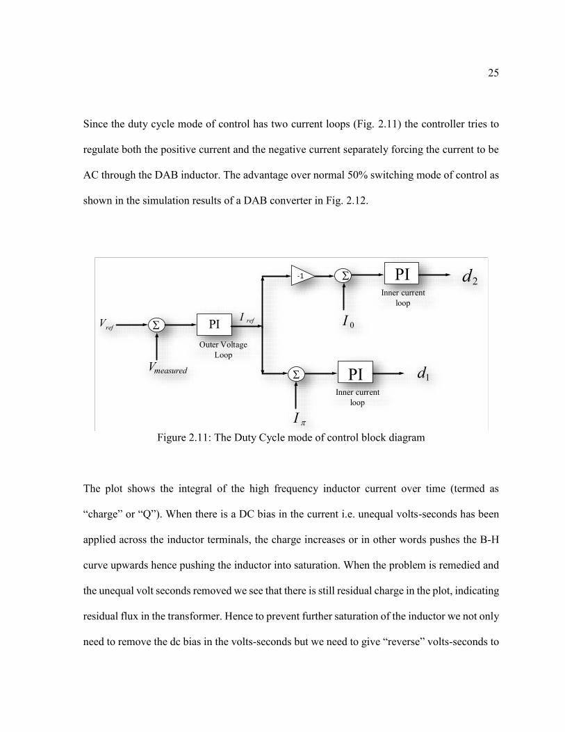
Since the duty cycle mode of control has two current loops (Fig. 2.11) the controller tries to
regulate both the positive current and the negative current separately forcing the current to be
AC through the DAB inductor. The advantage over normal 50% switching mode of control as
shown in the simulation results of a DAB converter in Fig. 2.12.
refV
measuredV
PI
Outer Voltage
Loop
refI
I
Inner current
loop
1d
0I
PI Inner current
loop
-12d
PI
Figure 2.11: The Duty Cycle mode of control block diagram
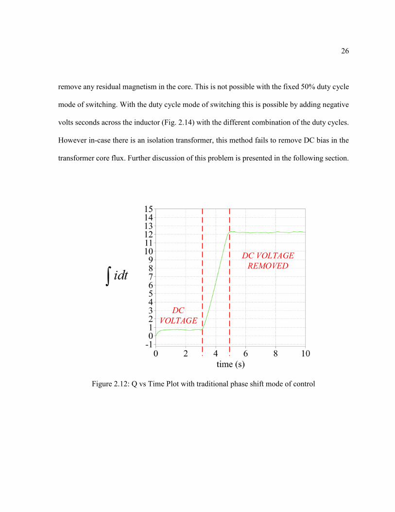
The plot shows the integral of the high frequency inductor current over time (termed as
“charge” or “Q”). When there is a DC bias in the current i.e. unequal volts-seconds has been
applied across the inductor terminals, the charge increases or in other words pushes the B-H
curve upwards hence pushing the inductor into saturation. When the problem is remedied and
the unequal volt seconds removed we see that there is still residual charge in the plot, indicating
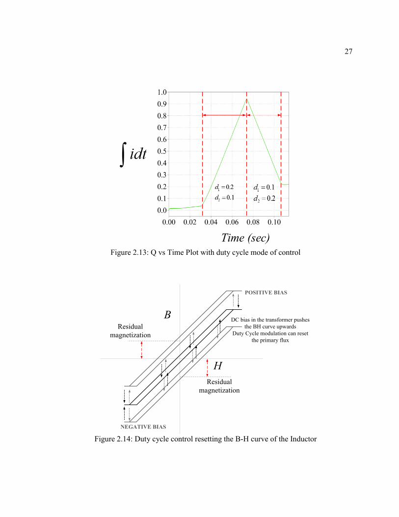
residual flux in the transformer. Hence to prevent further saturation of the inductor we not only
need to remove the dc bias in the volts-seconds but we need to give “reverse” volts-seconds to
26
remove any residual magnetism in the core. This is not possible with the fixed 50% duty cycle
mode of switching. With the duty cycle mode of switching this is possible by adding negative
volts seconds across the inductor (Fig. 2.14) with the different combination of the duty cycles.
However in-case there is an isolation transformer, this method fails to remove DC bias in the
transformer core flux. Further discussion of this problem is presented in the following section.
DC VOLTAGE
REMOVED
DC
VOLTAGE
Figure 2.12: Q vs Time Plot with traditional phase shift mode of control
27
Time (sec)
Figure 2.13: Q vs Time Plot with duty cycle mode of control
B
H
DC bias in the transformer pushes
the BH curve upwards
Duty Cycle modulation can reset
the primary flux
POSITIVE BIAS
NEGATIVE BIAS
Residual
magnetization
Residual
magnetization
Figure 2.14: Duty cycle control resetting the B-H curve of the Inductor

28
2.6. Contribution of magnetizing current in the HF DAB transformer
In the previous section the duty cycle mode of control was proposed which eliminates
the DC bias in the high frequency load current. However the DC bias in the magnetizing current
was not analyzed. Since dc bias in the magnetizing current and not the load current is
responsible for saturating the high frequency DAB transformer it is important to analyze which
bridge provides the magnetizing current to the transformer. This can be proved by analyzing
the T-model of the high frequency transformer (Fig. 2.15). It can be assumed without any loss
of generality that the primary side of the transformer has leakage kL and the secondary side (1-
k)L. The magnetizing inductance is Lm. Superposition principle is used to calculate the
magnetizing current. Considering the primary voltage Vprim the magnetizing current
contributed by the primary bridge 𝐼𝑚𝑝𝑟𝑖𝑚 is given by (2.7)
𝐼𝑚𝑝𝑟𝑖𝑚 = [
𝑉𝑝𝑟𝑖𝑚
𝑘𝐿 +(1 − 𝑘)𝐿𝐿𝑚(1 − 𝑘)𝐿 + 𝐿𝑚
](1 − 𝑘)𝐿
[(1 − 𝑘)𝐿 + 𝐿𝑚]
= 𝑉𝑝𝑟𝑖𝑚(1 − 𝑘)𝐿
𝑘𝐿[(1 − 𝑘)𝐿 + 𝐿𝑚] + (1 − 𝑘)𝐿𝐿𝑚 (2.7)
with = 1𝑦𝑖𝑒𝑙𝑑𝑠→ 𝐼𝑚
𝑝𝑟𝑖𝑚 = 0 . Thus from (2.7) we see that if the entire leakage is on the primary
side the secondary is the one supplying the magnetizing current and vice versa. The cause of
the DC bias in the DAB transformer has been analyzed in [17]. Since the primary switches are
switched at 50 % duty cycle semiconductor non-idealities may have a large contribution to the
DC flux in the transformer. The secondary side on the other hand is duty cycle modulated.

29
(a)
(b)
(c)
Figure 2.15: The T-model of the high frequency transformer with the distributed leakage
between the primary and the secondary
Hence any DC bias can be removed using controlled switching of the secondary switches. In
the following section several operating modes are shown based on the distribution of the

30
leakage inductance of the transformer and how each bridge contributes to the magnetizing flux
and what can be the possible control strategy to maintain the flux to be AC.
VoutVin
HF -transformer
S1,D1
S2,D2
S3,D3
S4,D4
S5,D5
S6,D6
S7,D7
S8,D8
(a) (b) (c)
Vin Vout Vin Vout Vin Vout
Figure 2.16: Equivalent circuit of the High frequency DAB transformer
2.6.1. Case 1: Entire Leakage is on primary side
The isolated DAB converter in Fig. 2.16 is considered as an example. In Fig. 2.16a the
entire leakage is on the primary side of the transformer. Hence the secondary side is supplying
the magnetizing current (Im shown in red). The load current Iload is shown in blue. Since the
secondary side is duty cycle modulated, both the magnetizing and the load current are functions
of the duty cycles d1 and d2. The secondary side can monitor the flux level in the transformer
core and adjust d1 and d2 so that there is no dc bias in the flux. The load current might have
DC offset generated by unequal volt-seconds from the primary that might saturate the inductor.

31
The duty cycles cannot be adjusted to compensate for this as it might inject DC flux in the
transformer. Thus this configuration of leakage inductance is not a good design to eliminate
DC bias. Implementing such a transformer is possible with coaxial wound transformer (CWT)
[18], [19], [20]. The CWT has the structural advantage that gives a control over the leakage
inductance of the transformer. Hence by designing the CWT as such we can precisely place
the leakage inductance of the transformer on the primary or on the secondary side.
2.6.2. Case 2: Entire Leakage is on secondary side
In the case that the entire leakage is on the secondary side (Fig. 2.16b) the load current
is still a function of the duty cycles but the magnetizing current is not. The magnetizing flux is
supplied by the primary bridge. Hence any unequal volt-seconds generated by the primary
bridge due to non-idealities in switching [17] will lead to a DC flux in the transformer. The
duty cycle modulation on the secondary will have no effect on the transformer flux. However,
it can still be implemented to prevent saturation in the secondary side leakage inductance. The
transformer bias can be eliminated by adding a positive or a negative bias in the primary
switching. The inductor bias can be eliminated separately by the duty cycle modulation.
2.6.3. Case 3: Distributed Leakage
In the case of distributed leakage (Fig. 2.16c), both the primary and the secondary side
has leakage inductance, and both the sides contribute to the magnetizing current. Hence non
idealities in both the primary and the secondary bridge contribute to the DC bias in the
transformer flux. Under such conditions the duty cycle modulation proposed earlier in the

32
secondary bridge will be unable to remove the DC flux in the transformer core. To remove the
DC flux an analog based controller is proposed (Fig. 2.17). Fig. 2.17 shows the controller for
flux control in the transformer core. It is assumed the primary is fixed at 50 % duty-cycle. The
secondary had a steady state duty cycle of 50 % onto which the controller adds ∆𝑑𝑠𝑒𝑐 . It is
assumed that the primary and the secondary switching non-idealities add together to produce
the unequal volt-seconds in the transformer core. The controller samples the primary current
and the secondary current and takes a difference which gives the magnetizing current 𝐼𝑚 .
Under ideal condition 𝐼𝑚 is AC or in other words the integral over one cycle (𝑄𝑐𝑦𝑐𝑙𝑒) will be
zero. However if either the primary or the secondary bridge generates unequal volts-seconds
then DC offset will appear. The controller compensates by comparing the 𝑄𝑐ℎ𝑎𝑟𝑔𝑒 to 0 by
producing an additional ∆𝑑𝑠𝑒𝑐 to nullify the effect. As a result (Fig. 2.19) the dc component
from the magnetizing current is channeled out to the load current which now contains the AC
and the DC component. Fig. 2.18 shows the simulation result for such a system. The simulation
shows the dc offset being removed from the magnetizing current but appearing on the load
current. Based on the amount of dc offset that is present in the load current the inductor may
saturate or operate at higher loss if there is air-gap to support DC flux. This is not desirable
and a solution is proposed in the following section.
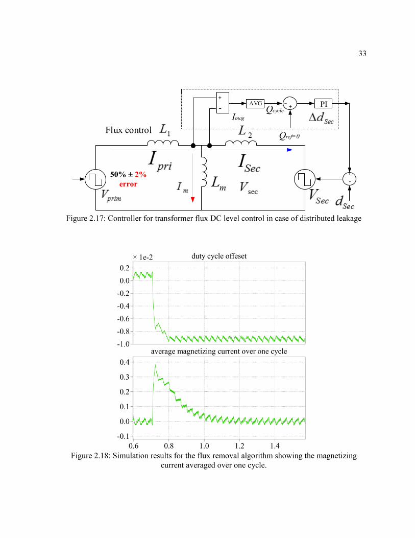
33
+
-AVG
+- PI
+
+
Flux control
50% ± 2%
error
Imag
Qcycle
Qref=0
Figure 2.17: Controller for transformer flux DC level control in case of distributed leakage
Figure 2.18: Simulation results for the flux removal algorithm showing the magnetizing
current averaged over one cycle.

34
Figure 2.19: Simulation results for the DC flux removal algorithm
2.6.4. Case 4: Duty Cycle mode of control with Flux control
In order to prevent DC bias in the load current that might saturate the DAB inductor a
duty based control is to be implemented on the secondary side. The assumption is that the
leakage inductance has to be on the secondary side. Hence the primary supplies the transformer
flux and the secondary controls the inductor flux (Fig. 2.20). The transformer flux is controlled
by adjusting the DC bias in the primary bridge. If the leakage inductance is on the secondary
side the primary bridge will provide the magnetizing current and control the transformer flux.
Using both these control mode taken together it is possible to completely remove any DC bias
either in the magnetizing current or the load current.
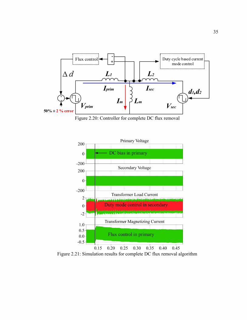
35
+
+
+-
Flux control
50% ± 2 % error
Duty cycle based current
mode control
Vprim Vsec
Iprim Isec
Im Lm
L1 L2
d1,d2
Figure 2.20: Controller for complete DC flux removal
DC bias in primary
Duty mode control in secondary
Flux control in primary
Figure 2.21: Simulation results for complete DC flux removal algorithm

36
Figure 2.22: Experimental results for DC flux removal algorithm
Fig. 2.22 shows the experimental results for the proposed controller. The current sensors used
for the purpose of measuring the high frequency DAB current are LEM sensors that output a
current signal that is first converted to a voltage signal by a loading resistor and then sent to
the ADC. By arranging the loading it is possible to isolate the magnetizing current and convert
it into voltage and provide it to the ACD for DC bias measurement. Fig. 2.22 shows the
experimental result of such an effort where the magnetizing current has been extracted from
the primary and the secondary current difference and the DC bias has been calculated and
compensation has been provided.
2.7. Predictive duty cycle mode of control
The efficacy of the duty cycle mode of control in removing the DC bias in the DAB
inductor has been shown in the previous section (Section 2.6.4). This provides the motivation
for developing a predictive algorithm for the duty cycle mode of control. Based on the control
strategy the duty cycle mode of control can be further classified in the following categories:

37
1) Half Cycle mode of control
2) Full cycle mode of control
3) Full Cycle equal area mode of control
2.8. Half cycle mode of control
In this mode of operation the sampling is done at two instances in the switching cycle, at
ωt = 0 and at ωt = π. The current sampled at ωt = 0 refers the current at ωt = π as the reference
and the current sampled at ωt = π refers the current sampled at ωt = 0 of the next cycle as the
reference (Fig. 2.23). The equations driving the controller are given in (2.8a) and (2.8b).
𝐼𝑟𝑒𝑓𝜋 = 𝐼0 +𝑚1𝑑1𝑇𝑠 +𝑚2 (
𝑇𝑠
2− 𝑑1𝑇𝑠) (2.8a)
𝐼𝑟𝑒𝑓0 = 𝐼𝜋 +𝑚1𝑑2𝑇𝑠 +𝑚2 (
𝑇𝑠
2− 𝑑2𝑇𝑠) (2.8b)
Where 𝑚1 =𝑉𝑖𝑛+𝑉𝑜𝑢𝑡
𝐿 , 𝑚2 =
𝑉𝑖𝑛−𝑉𝑜𝑢𝑡
𝐿 . This control is a deadbeat control as the response takes
place within one cycle. Since the positive reference is same as the negative reference in
magnitude, this makes sure that the current through the transformer is AC. Any DC component
is removed by changing the duty cycles (d1 & d2) accordingly. Fig. 2.24 shows the simulation
results of the transient response of the duty cycle modulated control. The reference current is
changed from -10 amps to - 5 amps at 𝜔𝑡 = 0 and from 10 to 5 amps at 𝜔𝑡 = 𝜋. It can be seen
from the simulation result that the sampled current changes the value within one switching
cycle (Fig. 2.24 green and red).

38
PI
Outer
Voltage
Loop
Predictive equation
(2.8b)-1
Predictive equation
(2.8a)
Figure 2.23: Controller diagram for the half cycle duty cycle mode of control
Time (seconds)
Tran
sfo
rmer
cur
rent
(A
mp
s)
Figure 2.24: Transient response of the half cycle duty cycle mode of control
2.9. Full cycle duty cycle mode of control
The full cycle duty cycle mode of control is different from the half cycle duty cycle mode
of control in the sense that the sampled current in one cycle is the reference current for the
previous cycle. The timing diagram for the full cycle mode of control is shown in Fig 2.25.

39
Two different timing modes are discussed here. One with the sampling done at the beginning
of the switching cycle (Fig 2.25) is using a down counter and another with sampling done at
the middle of a half cycle using an up-down counter (Fig 2.26). The advantage of using the up-
down counter is that the ADC can sample at the mid-point of the up count i.e. at count = N/2.
This mode is preferred, since that the current sampled will be free of switching transients
compared to the down counter used in Fig 2.25. Two up-down counters represented by the
two triangles offset by 180 (black or counter 1 and dotted blue or counter 2) are required in
this case as two currents are sampled, one in the positive half cycle and another in the negative
half cycle. The ADC samples when the counter is at 𝑁 2⁄ at up-count of the black counter or
counter 1. The sampled value is the current from the positive half cycle 𝐼𝑛1. Interrupt generated
at counter 1 = N does one set of the control calculations (2.9a). In the control calculations the
assumption is that the current in the next cycle i.e. 𝐼𝑛+1 1 will reach the desired reference value
generated by the outer voltage loop. The computed value is 𝑑𝑛+11 and is loaded to the compare
register of the counter 2. This generates the duty cycle for the counter 2 (the blue pulse in Fig.
2.26). Similar set of events take place with counter 2 one half-cycle earlier or later. The
negative current 𝐼𝑛−12 is sampled at up count of the counter 2. Interrupt is generated and the
control calculations take place at counter 2 = N and 𝑑𝑛2 is calculated (2.9b) which is loaded on
the compare register of counter 1 and generates the pulse shown in black (Fig. 2.26). The
control calculations for the full cycle duty cycle mode are as follows
𝐼𝑛+1[𝑟𝑒𝑓]1 = 𝐼𝑛
1 +𝑚2𝑇𝑠
4−𝑚1𝑑𝑛
2𝑇𝑠 −𝑚2 (𝑇𝑠
2− 𝑑𝑛
2𝑇𝑠) + 𝑑𝑛+11 𝑇𝑠 + 𝑚2 (
𝑇𝑠
4− 𝑑𝑛+1
1 𝑇𝑠) (2.9a)
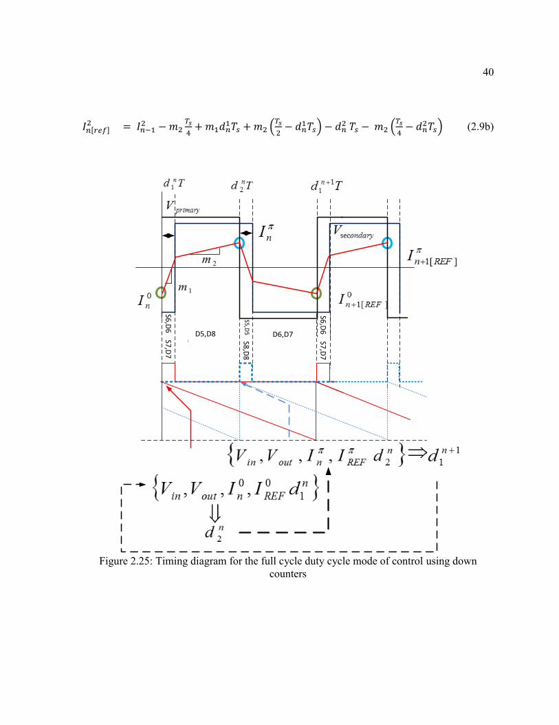
40
𝐼𝑛[𝑟𝑒𝑓]2 = 𝐼𝑛−1
2 −𝑚2𝑇𝑠
4+𝑚1𝑑𝑛
1𝑇𝑠 +𝑚2 (𝑇𝑠
2− 𝑑𝑛
1𝑇𝑠) − 𝑑𝑛2 𝑇𝑠 − 𝑚2 (
𝑇𝑠
4− 𝑑𝑛
2𝑇𝑠) (2.9b)
S6,D6
S7,D7
D5,D8
S5,D
5S8,D
8
D6,D7
S6,D6
S7,D7
Figure 2.25: Timing diagram for the full cycle duty cycle mode of control using down
counters
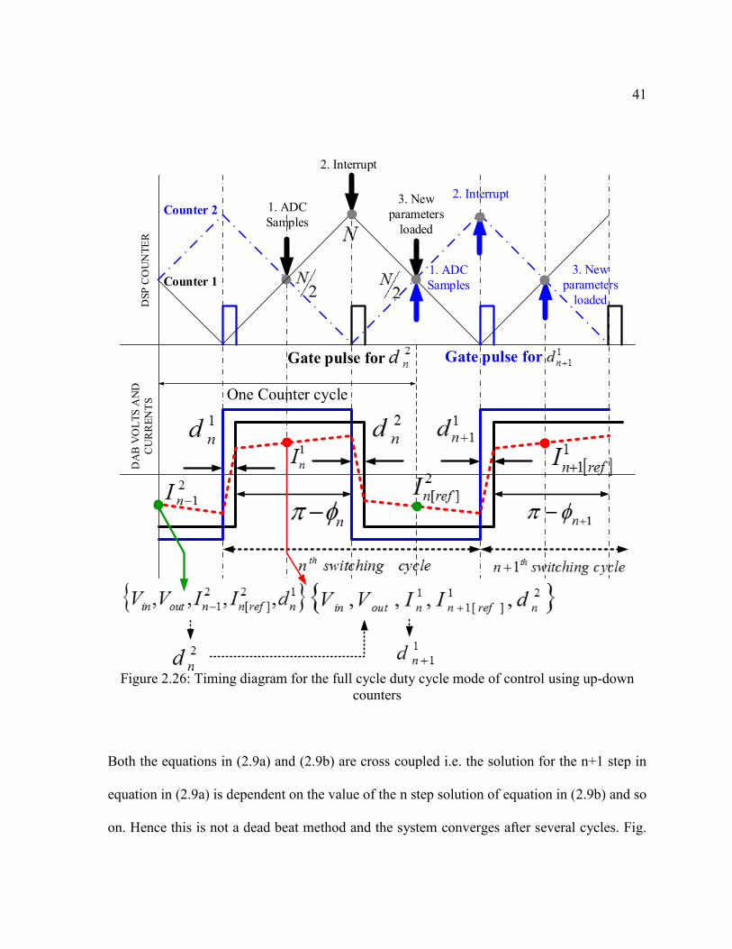
41
One Counter cycle
DS
P C
OU
NT
ER
DA
B V
OL
TS
AN
D
CU
RR
EN
TS
3. New
parameters
loaded
1. ADC
Samples
2. Interrupt1. ADC
Samples
2. Interrupt
3. New
parameters
loaded
Gate pulse for Gate pulse for
Counter 2
Counter 1
Figure 2.26: Timing diagram for the full cycle duty cycle mode of control using up-down
counters
Both the equations in (2.9a) and (2.9b) are cross coupled i.e. the solution for the n+1 step in
equation in (2.9a) is dependent on the value of the n step solution of equation in (2.9b) and so
on. Hence this is not a dead beat method and the system converges after several cycles. Fig.

42
2.27 shows the simulation result of the full cycle duty cycle mode of control. The transformer
current is given a DC bias by switching off one of the devices in the primary of the DAB. The
device is then turned on and it can be seen from the simulation result in Fig. 2.27 that the DC
bias is removed within one switching cycle of the converter. Although this method is
computationally simple, the current needs to be sampled twice in every switching cycle and
with high frequency that may be difficult. Hence an alternate method is proposed where the
current is sampled just once in the switching cycle and still the current is forced to be AC. The
method is equal area method and is proposed in the following section.
Figure 2.27: Simulation result for the full cycle duty cycle mode of control

43
2.10. Equal area mode of control
The equal area mode of control is an extension of the duty cycle mode of control. The
idea is to sample the current at the start of the switching cycle and make it to follow a reference
current that comes from the voltage PI controller. Considering the nth switching cycle and the
(n+1)th cycle, we can get the following equation for the current:
𝑖𝑛+1 = 𝑖𝑛 +𝑉𝑖𝑛 + 𝑉𝑜𝑢𝑡
𝐿𝑑1𝑇𝑠 +
𝑉𝑖𝑛 − 𝑉𝑜𝑢𝑡𝐿
(𝑇𝑠2− 𝑑1𝑇𝑠) −
𝑉𝑖𝑛 + 𝑉𝑜𝑢𝑡𝐿
𝑑2𝑇𝑠
−𝑉𝑖𝑛 − 𝑉𝑜𝑢𝑡
𝐿(𝑇𝑠2− 𝑑2𝑇𝑠) (2.10)
sTd1
primaryV
ondaryVsec
1A
2A3A
4A
ss Td
T1
2
sTd2
ss Td
T2
2
sampledI ][refI
Figure 2.28: Equal area mode of control

44
Assuming that in one cycle the corrective action is achieved and the above equation simplifies
as shown in (2.11)
(𝐼𝑟𝑒𝑓 − 𝐼𝑛)𝐿
2𝑉𝑜𝑢𝑡𝑇𝑠= 𝑑1 − 𝑑2 (2.11)
This is not enough to calculate the value of the duty cycles since there are two unknowns and
one equation (2.11). This can be used to make the current through the transformer a perfect
AC i.e. remove any DC offset in it. That can be done by equating the area under the curve of
current in the positive half cycle (Fig. 2.28) (𝐴1 + 𝐴2) to that of the negative half cycle
(𝐴3 + 𝐴4) i.e.
4321 AAAA (2.12)
Here (𝐴1 + 𝐴2) is a function of d1 and (𝐴3 + 𝐴4) is a function of d2. So from equations in
(2.11) & (2.12) we get the solutions for d1 and d2 as in (2.13).
outsrefnout
outsoutins
outsrefnout
outsrefrefrefnn
outsrefnout
outsoutinsoutsref
outsrefnout
outsnrefrefnn
VTLILITV
VTVVT
VTLILITV
VLTILILIILId
VTLILITV
VTVVTVLTI
VTLILITV
VLTILILIILId
44
42
4
2
4
22
22222222
2
22222222
1
(2.13)
The duty cycle values are loaded in the corresponding counters and the gate pulses are
generated. Fig. 2.29 shows the transient response for the equal area mode of control. The
current through the transformer in the DAB was intentionally given a DC bias by turning off
one of the switches on the primary side. The switch was then turned on and the predictive

45
controller is able to remove the dc bias in once cycle. The same exercise was done with a
simple voltage based control and it is seen that it takes much more time for the controller to
fully remove the DC bias in the current.
Figure 2.29: Transient response of the equal area mode of control
The Fig. 2.28 shows the equal area mode of control with instant update. However the
controlling point may be two cycles down the line of the sampling point as shown in Fig. 2.29
with 𝐴1 + 𝐴2 + 𝐴5 + 𝐴6 = 𝐴4 + 𝐴3 + 𝐴7 + 𝐴8
Predictive controller turned on
DC bias given to transformer current

46
Figure 2.30: Equal area mode of control with control point two cycles down the line
2.11. Power mode of predictive control
So far the predictive controller regulates a particular current peak point within a cycle.
But in case where there is power sharing required between parallel connected DAB converters
(Fig. 2.31), this mode of control is not suffice. Here power balancing requirement is critical if
the converters input stage is series connected to block higher DC bus voltage. The previously
discussed methods will force the peak point currents to a referenced value. If the referenced
value is at 𝜔𝑡 = 𝜑 where 𝜑 is the phase shift, then the expression of the current at that point
is given as (2.14).
𝐼𝜑 =𝑉𝑖𝑛𝜔𝐿[𝑉𝑜𝑢𝑡𝑉𝑖𝑛
𝜑 +𝜋
2(1 −
𝑉𝑜𝑢𝑡𝑉𝑖𝑛)] (2.14)

47
Figure 2.31: Power Balance in series input parallel output DAB stages
Considering multiple DAB connected with series input, parallel output mode with different
leakage inductances (𝐿1,𝐿2…), the predictive controller with the current reference tracking,
will force the individual DAB to work at different phase shift angles (𝜑1, 𝜑2, … ) where
according to (2.15),
𝜑1𝐿1⁄ =
𝜑2𝐿2⁄ = ⋯ (Assuming 𝑉𝑖𝑛 = 𝑉𝑜𝑢𝑡) (2.15)
But the power transfer equation for the DAB is given as (2.16).
𝑃𝑡𝑟𝑎𝑛𝑠𝑓𝑒𝑟𝑟𝑒𝑑 =𝑉𝑖𝑛𝑉𝑜𝑢𝑡𝜔𝐿
𝜑 (1 −𝜑
𝜋) (2.16)

48
Hence for power balance in parallel connected DAB the relationship between the phase shift
angle and the leakage inductance turns out as (2.17)
𝜑1𝐿1(1 −
𝜑1𝐿1) =
𝜑2𝐿2(1 −
𝜑2𝐿2) = ⋯ (2.17)
Since the relationship mentioned in 2.15 ≠ 2.17 therefore the control modes discussed above
is not suffice for power mode control. For that a different approach has to be taken that is
somewhat similar to the area mode control discussed in the previous section. Fig. 2.33 shows
the controller block diagram.
Figure 2.32: Power mode of predictive control
swTd 1
primaryV
ondaryVsec
1A
2A
swsw Td
T1
2
3A
4A
swTd 2
swsw Td
T2
2
nI1nI

49
The current is sampled at 𝜔𝑡 = 0. An external voltage loop provides the power reference (Fig
2.33). With the generated Pref and the I0 from the sampled current the controller calculates the
required phase shift angle to produce the required power by calculating the area under the curve
in the positive half cycle (yellow shaded portion in Fig. 2.32).
Figure 2.33: Controller block diagram for the power mode of predictive control
The phase shift angle calculated from the power mode control is given as (2.18).
𝜑 = 𝜋 − √𝜋√𝜋𝑉𝑖𝑛∆𝑉1 − 2𝜔𝐿𝑃𝑟𝑒𝑓 + 2𝐼0𝜔𝐿𝑉𝑖𝑛
𝑉𝑖𝑛(∆𝑉1 − ∆𝑉2) (2.18)
Where ∆𝑉1 = 𝑉𝑖𝑛 + 𝑉𝑜𝑢𝑡 and ∆𝑉2 = 𝑉𝑜𝑢𝑡 − 𝑉𝑖𝑛 . This shows the relation of the phase angle
with power is quadratic in nature as the way it should be from (2.16).
2.12. Experimental verification of predictive control
This section of the chapter presents the experimental verification of the predictive
controller. In order to show the efficacy of the predictive controller, a step change in the current
PI
measuredV
refPPredictive
law
refV
oI

50
reference was provided. If working properly, the controller will be able to track the change in
one cycle (deadbeat control).
Figure 2.34: Transient test of the half cycle phase shift current mode control
Fig. 2.34 shows the step change in the current reference from the controller and the converter
tracking the change in one cycle in deadbeat fashion. The control algorithm is mentioned in
section 2.4.2 and equation (2.2a). The current is sampled at 𝜔𝑡 = 0 and referenced at 𝜔𝑡 =
𝜑. Based on the reference value the phase shift angle has been calculated. In the setup the
input voltage is 120V, the switching frequency is 10 kHz, the leakage inductance of the
transformer is 0.77 mH. The current reference is changed in step from 1A to 2A.

51
Figure 2.35: Transient test of the half cycle phase shift current mode control showing the 𝐿 𝑅⁄
decay.
Fig. 2.35 shows the zoomed out view of the current response. This shows the 𝜏 = 𝐿 𝑅⁄ decay
time for the current. In this present case the transformer shows a leakage resistance of 0.3 Ω.
In an ideal transformer the resistance is supposed to be negligible. Hence the step change on
the current reference will introduce a slowly decaying AC waveform. In an ideal transformer
as 𝑅 → 0, 𝜏 → ∞. Hence the transformer current will have a permanent DC offset. This might
lead to saturation of the transformer or higher losses due to the DC offset. To remedy that the
duty cycle mode of control was proposed in section 2.5. The predictive half cycle mode of
control proposed in section 2.8 has been implemented in the experimental setup. The current
sampled at 𝜔𝑡 = 0 is referenced to the current at 𝜔𝑡 = 𝜑 and the current sampled at 𝜔𝑡 = is
referenced to current sampled at 𝜔𝑡 = 𝜋 + 𝜑. Here 𝜑 represents the phase shift angle that

52
would have manifested in the phase shift mode of control. The controller equations are similar
to that in 2.8a and 2.8b and hence is not further derived.
Line
Current
Line
Voltage
Figure 2.36: Transient test of the half cycle duty cycle current mode control.
Fig. 2.36 shows the experimental result for the duty cycle mode of control. The important
difference to the previous result is the absence of the 𝐿 𝑅⁄ decay. Since the duty cycle of the
secondary bridges are operating independently, the current changes both in the positive and
the negative half cycle. The controller that has been used is the TMS320F28335. Since this
mode requires double sampling with in one switching cycle, the interrupt is called based on
the ADC EOC. The ADC SOC is triggered by the EPWM modules as per the Fig. 2.25. The

53
red down counter corresponds to EPWM 1 while the blue counter corresponds to EPWM 3
phase shifted by π. ADC SOC is triggered every time EPWM 1 counter reaches the period
value and EPWM 3 counter reaches the period value. These SOC signals are OR-ed in the DSP
and hence sampling take place two times in the cycle, once at 𝜔𝑡 = 0 and 𝜔𝑡 = 𝜋. The load
mode registers in the EPWM modules are set to load the compare values in the registers
immediately further reducing delay. Fig. 2.37 shows the duty cycle change with the step change
in the current reference value from 1A to 2A. The predictive controller still requires an
inductance information to operate optimally. However the leakage inductance of the
transformer may change with time due to different causes. Hence a compensation algorithm
was proposed in section 2.4.3 and simulation verification was shown in Fig. 2.7. However it
requires further sampling at the point of referencing. In the experimental setup a simpler
algorithm was implemented. Since in the first half cycle the current was sampled at 𝜔𝑡 = 0
and referenced at 𝜔𝑡 = 𝜑, it is first assumed that the current has reached the required reference
at 𝜔𝑡 = 𝜑. With this assumption the current at 𝜔𝑡 = 𝜋 is calculated as per (2.19).
𝐼𝜋𝑐𝑎𝑙𝑐 = 𝐼𝑟𝑒𝑓 +
∆𝑉2𝐿𝐷𝑆𝑃
(1
2− 𝑑1) 𝑇𝑠 (2.19)
Here ∆𝑉2 = 𝑉𝑜𝑢𝑡 − 𝑉𝑖𝑛 and 𝐿𝐷𝑆𝑃 (≠ 𝐿𝑎𝑐𝑡) is the erroneous inductance value input to the
controller and 𝑑1 is the duty cycle calculated from the predictive controller as per equations
(2.8a) and (2.8b). If 𝐿𝐷𝑆𝑃 = 𝐿𝑎𝑐𝑡 in that case 𝐼𝜋𝑐𝑎𝑙𝑐 = 𝐼𝜋
𝑟𝑒𝑓. In order to compensate for the
change in the inductance value with time a compensation loop is run parallel to the controller
with a slower bandwidth. The output of the compensator is ∆𝐿 which is added to 𝐿𝐷𝑆𝑃 and

54
replaces L in (2.8a) and (2.8b). Fig. 2.38 shows the controller block diagram for the
compensation for the inductance error in the controller.
Duty
cycle d1
Duty
cycle d2
Line
Current
Figure 2.37: Transient test of the half cycle duty cycle current mode control along with the
changes in the duty cycles d1 and d2
Fig. 2.39 shows the experimental result for the compensation loop implemented in the
controller. The measured transformer leakage inductance is 0.936 mH and the erroneous
inductance value was set as 0.7 mH. It is seen that the controller compensates for the error by
introducing the ∆𝐿 which gets added to 𝐿𝐷𝑆𝑃 to track the reference correctly.

55
S6,D6
S7,D7
D5,D8S5
,D5
S8,D
8D6,D7
S6,D
6S7
,D7
PI
SOC1
EPWM1 EPWM3
SOC3
Figure 2.38: Controller diagram for the leakage inductance error compensation

56
Figure 2.39: Transient test of the leakage inductance error compensation
2.13. Conclusions
In this chapter the digital predictive current mode control have been applied to the DAB
converter. The main results obtained in this chapter is summarized as follows:
A predictive phase shift controller was proposed for the dual active bridge
converter. The controller is of dead beat in nature and updates the control variable
in one cycle.
The controller was shown to be sensitive of the leakage inductance value of the
transformer hence a compensation loop was implemented to make the system
insensitive of the change in inductance value.

57
A duty cycle mode of control was proposed for the Dual Active Bridge Converter.
The proposed control was shown to remove any DC bias in the transformer current
by adjusting the duty cycles independently.
A predictive duty cycle mode of control was proposed. The proposed control was
shown to be dead beat in nature. In order to remove the DC bias in the transformer
current an equal area criterion was imposed to calculate the duty cycles. The equal
area criterion forces the area under the DAB transformer current waveform to zero
to remove unwanted DC bias.
A power based predictive controller was proposed that predicts the phase shift angle
based on the required power transfer. The power based controller was shown to
have second order response due to the quadratic nature of the power angle curve.
Experimental verification of the phase shift predictive controller was performed. A
step change in the current reference was provided and the controller was shown to
follow the reference in one cycle. However a 𝐿 𝑅 ⁄ decay was shown to exist in the
current as per the transformer 𝐿 𝑅⁄ time constant.
Experimental verification of the duty cycle mode of control was performed. With
a step change in the current reference, the controller was shown to respond within
one switching cycle. Due to the asymmetric variation in the duty cycle, the current
waveform was shown to be free of the 𝐿 𝑅⁄ transient, which was otherwise present
in the phase shift predictive current mode control.

58
An analysis was done to understand the contribution of the primary and the
secondary bridges in supplying the magnetizing current of the high frequency
transformer in the DAB. A method was proposed to sense the DC bias in the current
by implementing a moving window average on the magnetizing current and a
compensating DC offset was then given to the primary or the secondary switches
to remove any unwanted DC bias in the magnetizing current.

59
Chapter 3 Multi-terminal application for the Dual Active Bridge
converter for multiple Renewable Energy Source integration
3.1. Introduction
In this chapter of the thesis a multi-terminal DAB is considered with multiple inputs and
single output for the purpose of renewable energy integration. Extensive research has been
done on the integration of renewable energy sources (RES) to a common DC bus using parallel
DC to DC converter [11]. DC droop control or master slave mode of control is employed for
power sharing between the parallel DC to DC converters. The introduction of the SST concept
[21], has provided the motivation of integrating the renewable energy sources directly into the
high frequency magnetic stage of the topology, i.e. the DAB stage. This provides the benefit
of galvanic isolation using minimum magnetic component. Integration of multiple renewable
energy sources in the DAB topology is an interesting topic of research. In [13] several multiport
DAB topology has been mentioned. In [4] and [12] a gyrator based concept for the multiport
DAB topology has been proposed. Since RES may have fluctuating voltage profile due to the
intermittency of power available, when source voltage magnitudes are different the single core
topology [13] will drive a reactive current through each of the source bridges leading to losses.
In this chapter a flux accumulation based approach has been followed to decouple individual
RES from each other. This has been achieved using a multi-limb-core transformer based
topology. It is fundamentally a multi terminal DAB converter with multiple primaries and a
single secondary. Power transfer take place between the primary and secondary using phase

60
shift modulation. Instead of the primaries linking a single core, they are all linked to different
cores that are connected to a central limb, to which the secondary winding is connected. This
central limb acts as a flux accumulator. Equivalent circuit of the topology has been derived to
explain the decoupling of the individual RES. A PWM based switching strategy has been
proposed to control the source current in order to operate the RES at their individual maximum
power point.
3.2. Circulating current in a single limb core topology
The circulating current in a single limb core based topology is the motivation driving the
research in this chapter. This section discuses in more detail the single limb core topology. Fig.
3.1 shows the single limb core based multi-active bridge topology. Circulating current will
exist between the primaries provided 𝑉1 ≠ 𝑉2 ≠ 𝑉3 ≠ 𝑉4 . The circulating current not only
depends on the magnitude of the voltage mismatch but also on the leakage inductances linking
the individual windings (Fig 3.2). However the circulating power is also a function of how the
leakage is distributed in the windings. This provides the motivation of understanding how the
distribution of leakage will affect the circulating current which has been discussed in section
3.3 and 3.4.

61
LO
AD
Renew
able
Sourc
es
Magnetic path through HF
transformer
Figure 3.1: The Multi-Active Bridge converter concept based on a single limb core topology
V
V
fL
VI pk
4
Vo
ltag
e, c
urr
ent
V1
V2
Q
P
P
Vprim1
Vprim2
Figure 3.2: Circulating current due to voltage mismatch

62
3.3. Leakage inductance distribution and the impact on the circulating reactive
power
Leakage inductance of the primary and the secondary windings are the most important
factor in determining the circulating reactive power in the system. For simplicity the triple
active bridge system is considered (Fig. 3.2) with two primaries and one secondary. The
equivalent diagram of the system is shown in Fig. 3.3.
S2
Superposition 2
xL
(1-x)L(1-x)L
S3
Superposition 3
xL
(1-x)L(1-x)LS1
Superposition 1
xL
(1-x)L(1-x)L
Figure 3.3: Circulating current due to voltage mismatch in the primaries
The three bridges are voltage sourced hence modelled by voltage sources 𝑆1, 𝑆2 for primary 1
and primary 2 and 𝑆3 for the secondary lagging bridge. The leakage inductance can be
considered to be distributed between the primaries and the secondary as shown in Fig. 3.3. A
symmetrical distribution is considered to make the calculations simpler. In order to calculate
the reactive power supplied by the sources the superposition theory is used. The superposed
S 1 S3 S2
Equivalent electrical circuit for the
SLC converter
xL (1-x)L(1-x)L

63
circuits are shown in Fig. 3.3. The current supplied by the sources are given as 𝐼1for source 𝑆1,
𝐼2for source 𝑆2 and so forth. The net current then can be calculated according to the
superposition theory. 𝐼𝑆1 is the net current for source 𝑆1, 𝐼𝑆2for source 𝑆2 and so forth. 𝑄1 is
the reactive power supplied by the source 𝑆1 , 𝑄2 by source 𝑆2. 𝑃1 is the real power supplied
by the source 𝑆1, 𝑃2 by source 𝑆2. δ is the phase lag in radians of the secondary bridge with
respect to the primary bridges. ω is the switching frequency of the converter in radians per
second. It can be mathematically derived from the expressions of the reactive powers that both
𝑄1 and 𝑄2 has a minimum with x = 0. Hence the entire leakage of the individual windings has
to be on the primary side with minimum possible leakage on the secondary. This is possible
with a coaxial winding transformer (CWT). The following section proposes the CWT based
topology in details.
3.4. Coaxial Winding transformer (CWT) based topology
The coaxial based topology has been shown in Fig. 3.4. In a CWT based topology the
transformer leakage inductance can be controlled by changing the radii of the primary or the
secondary conductors (3.1) [20].
𝐿𝑙𝑒𝑎𝑘𝑎𝑔𝑒 = 𝑘𝑙𝑛𝑟2𝑟1 (3.1)
In order to keep the leakage on the primary side, the primary conductor is kept within the
secondary conductor. Fig. 3.4 shows the topology of the CWT based accumulator. The
different primary bridges are connected to different RES forming accumulator concept. Since

64
RES are the primary sources, MPPT operation becomes an important aspect for the topology
to handle. An MPPT driven input DC current control has been investigated in the following
section to make each primary operate at different phase angle (δ) to supply the power available.
The following section treats the concept in details.
Table 3.1: Current and power contributed by each source in the multi-active bridge topology
One of the bridges can be connected to a battery as shown in Fig. 3.4 and act as energy storage
in times of excess generation. One of the bridges is connected to the primary side rectifier and
can be used to send back power to the grid or take power from the grid should the need arise.
Since the bridges are connected to RES, hence the MPPT operation becomes an important
Parameters Values
𝐼1 𝑉1
𝑗(1 − 𝑥2)𝜔𝐿
𝐼2 𝑉2
𝑗(1 − 𝑥2)𝜔𝐿
𝐼𝑆1 𝐼1 −𝐼32− 𝑥𝐼2
𝐼𝑆2 𝐼2 −
𝐼32− 𝑥𝐼1
𝑃1 −𝑉1𝑉3 sin 𝛿
(𝑥 + 1)𝜔𝐿
𝑃2 −𝑉2𝑉3 sin 𝛿
(𝑥 + 1)𝜔𝐿
𝑄1 𝑉12 − (𝑥𝑉1𝑉2) − 𝑉1𝑉3(1 − 𝑥) cos 𝛿
(1 − 𝑥2)𝜔𝐿
𝑄2 𝑉22 − (𝑥𝑉1𝑉2) − 𝑉2𝑉3(1 − 𝑥) cos 𝛿
(1 − 𝑥2)𝜔𝐿
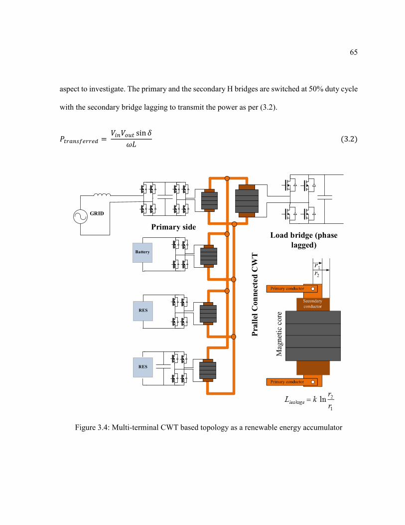
65
aspect to investigate. The primary and the secondary H bridges are switched at 50% duty cycle
with the secondary bridge lagging to transmit the power as per (3.2).
𝑃𝑡𝑟𝑎𝑛𝑠𝑓𝑒𝑟𝑟𝑒𝑑 = 𝑉𝑖𝑛𝑉𝑜𝑢𝑡 sin 𝛿
𝜔𝐿 (3.2)
Load bridge (phase
lagged)
Pra
llel
Co
nn
ect
ed
CW
T
GRID
RES
Primary side
RES
Battery
Figure 3.4: Multi-terminal CWT based topology as a renewable energy accumulator

66
3.5. Input current control in the CWT based topology
Without a loss of generality we can assume that each RES operates at different operating
point which translates into different δ as per (3.2). Fig. 3.5 proposes the control scheme for
the CWT based topology schematically. Since the entire leakage is assumed to be on the
primary side each primary is decoupled from the other primary and power transfer only takes
place between individual primary and the secondary. The equivalent electrical circuit for the
fundamental frequency is given in Fig. 3.5. Since each sub circuit is completely decoupled
from each other there is no circulating reactive power between the primaries due to DC bus
voltage mismatch. As per in Fig.3.5 the entire circuit can be separated out into 4 sub-circuits,
one for each primary. 𝐿1, 𝐿2… are the leakage associated with each primary. The power
transferred is as per (3.2). The total power transferred to the secondary is
𝑃𝑇𝑂𝑇𝐴𝐿 =∑𝑉𝑃𝑅𝐼𝑀𝑖𝑉𝑆𝐸𝐶𝑠𝑖𝑛𝛿𝑖
𝜔𝐿𝑖 (3.3)
4
𝑖=1

67
Pra
llel
Co
nn
ect
ed
CW
T
GRID
Primary side
RES1
Battery
RES2
PI
2measuredI
2REFI
MPPT
2
refV
measuredV
PI
load
Figure 3.5: Input current control operation on the CWT based topology
3.6. Series connected transformer based topology
The coaxial based design for a high frequency transformer has several disadvantages.
Some of the disadvantages have been explained in [20]. They are:
1. Edge effect
2. Limit in the number of turns.
The edge effect as mentioned in [20], shows that the leakage is considerable on the edges of
the transformer than the inside of the cylinder. Hence there is a requirement of adding more
magnetic core element in the transformer core to achieve significant self-inductance on the

68
primary side. Adding more core material increases weight and for applications where weight
saving is a concern, this becomes a problem. The limit in the number of turns is a fundamental
problem for the coaxial transformer. In Fig. 3.5 we see a 1:1 configuration. However in case a
step up in voltage is required it is desirable to add more number of turns to the secondary side
of the transformer. This will add more unwanted leakage inductance on the secondary side.
The decoupled sub-circuit assumption will no longer remain valid (Fig.3.5). Due to these
disadvantages a series connected topology has been proposed.
Series connected topology
Grid Side
Battery
Output
Inverter
RES 3
RES 2
Vprim1
Vprim2
Vprim3
Vprim4
Vsec
Llumped
Figure 3.6: The series connected topology

69
The series connected topology and the equivalent circuit is shown in Fig. 3.6. All the high
frequency primary voltages are in series and in phase. Therefore the fluctuation in the voltage
does not drive any additional reactive power between the primary voltages. Unlike the CWT
topology the leakage inductance can be distributed between the primary and the secondary.
Hence the transformer design becomes much easier. The number of turns can be manipulated
to achieve the necessary voltage step up on the secondary side. The power transfer between
the primaries and the secondary take place through the lumped inductor (Llumped) in Fig. 3.6
which is the sum total of all the leakage inductances of all the windings (primary and
secondary). Provided there is no phase shift between the primary voltages, and the secondary
voltage lags the primary by angle δ, the power transfer is given by (3.4).
𝑃𝑇𝑂𝑇𝐴𝐿 =(∑ 𝑉𝑝𝑟𝑖𝑚 𝑖
4𝑖=1 )𝑉𝑠𝑒𝑐 sin 𝛿
𝜔𝐿𝑙𝑢𝑚𝑝𝑒𝑑 (3.4)
The different functionalities of the accumulator topology have been laid out in the introduction
of the paper. One of the principle functionality of the accumulator is to have MPPT based
current or voltage control to make the RES deliver the maximum power under any voltage.
MPPT operation was possible on the CWT topology. The MPPT operation for the series
connected topology is discussed in the following section.
3.7. Input current control in the series connected topology
Input current control is possible in the series connected topology using duty cycle
modulation as shown in Fig.3.7.

70
pole
S1
D1
S2
D2
S3
D3
S4
D4
RES
S1
S4
S1
D3
S3
S2
D4
S2
Pole A Pole B
Figure 3.7: The Duty Cycle modulation to implement input current control
Fig. 3.7 shows the schematic of the duty cycle mode of control to achieve the input current
regulation. A phase shift is given in the primary poles as shown in Fig. 3.7. A pole to pole
phase shift (i.e. between Pole A and Pole B) of π implements the 50 % voltage waveform. If
the pole phase shift is less than π we get a zero level in between. This dead time is created
when the current from the winding circulates between the switches and the diodes (S1, D3) or
(D1, S3). Many such combinations exist depending on the current direction and the previous
switching state. This switching strategy helps to partially decouple the input current from the
winding current as per (3.5).
𝐼𝑠𝑜𝑢𝑟𝑐𝑒 =𝜑𝑝𝑜𝑙𝑒
𝜋𝐼𝑤𝑖𝑛𝑑𝑖𝑛𝑔 (3.5)

71
Without the loss of generality it can be considered that one of the RES connected to the
peripheral winding and the H-bridge needs to operate at a lower 𝐼𝑟𝑒𝑓 generated from the MPPT
algorithm, while the rest of the peripheral windings have a pole phase shift of π. In Fig. 3.7 the
green is the winding current common to all peripheral and central winding. For the bridge that
does MPPT we have 𝜑𝑝𝑜𝑙𝑒 ≤ 𝜋 . For that bridge (Fig. 3.7) at the beginning of the switching
period S1 and S4 are turned on and pole to pole voltage is 𝑉𝐷𝐶 . During this time the winding
current flows through the switches S1 and S4 (red arrow in Fig. 3.7) and the source. Hence the
source supplies power. Then after 𝜔𝑡 = 𝜑𝑝𝑜𝑙𝑒 the switch S4 is turned off. Since at this time the
current is positive, it forward biases the diode D3 and flows through it. Thus it introduces a
zero state in the pole to pole voltage. The winding current then circulates through S1 and D3
(dotted line in Fig. 3.7). The source does not provide any current at that instant and is
disconnected. Thus by controlling 𝜑𝑝𝑜𝑙𝑒 we can control the amount of current drawn from the
source and implement MPPT. Since 𝜑𝑝𝑜𝑙𝑒𝑀𝐴𝑋 = 𝜋 we have an upper limit on the MPPT current
which is equal to the input current of the other RES with the bridges operating at 𝜑𝑝𝑜𝑙𝑒 = 𝜋.
Experimental results validating the control scheme will be shown at the later sections on a low
voltage prototype.
3.8. A multi-limb transformer topology
In this section an alternate to the series connected topology has been proposed. The multi
limb core topology [22] is shown in Fig. 3.8. The peripheral limbs have windings that are
connected to H-bridges connected to RES, battery or grid tied. The peripheral limbs generate

72
the flux that is accumulated in the central limb. The winding in the central limb is connected
to the H-bridge that is connected to the output load. The primary bridges are switched at 50 %
duty cycle. There is no phase difference between the primaries. The secondary is lagged with
respect to the primary to regulate the output voltage. Hence the switching is exactly similar to
the series connected topology. The 5-limb core structure is shown in Fig. 3.8. The primary
sources are connected to the peripheral limb via H-bridge while the central limb accommodates
the secondary winding. One of the primaries is connected to energy storage. An electrical
equivalent circuit is derived in the following section which show how each individual voltage
sources, although connected by the fused magnetic structure, is decoupled. The magnetic
equivalent circuit of the MLC based topology is shown in Fig 3.9. It is functionally similar to
the series connected topology. The similarity is explained in the following section.
Secondary /Load
primary /source
primary /source
primary /source
Battery /source/load
Figure 3.8: The MLC based topology

73
Figure 3.9: Electrical equivalent of the MLC topology
3.9. Electrical equivalent circuit of the MLC topology
Fig. 3.9 shows the magnetic equivalent circuit for the MLC transformer in terms of
modular cores. Since the interface between the electrical stage and the magnetic stage acts as
a natural gyrator, bond graph model is an effective approach to derive the equivalent model of
the system [23], [24], [25]. A simpler three limb core topology was considered for the bond
graph analysis. Using the natural gyrator principle the bond graph for the three limb core
transformer was developed.
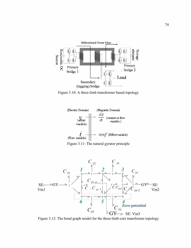
74
Figure 3.10: A three-limb transformer based topology
Figure 3.11: The natural gyrator principle
SE:
Vin1
GY 1 1
0 1 0 1 0
1 1
0 1 0 1 0
1
GY
GY SE:
Vin2
1 2 3
456
1
Zero potential
SE: Vin3 Figure 3.12: The bond graph model for the three-limb core transformer topology

75
SE:
Vin1GY 1
0 1 0 1 0
11 GY GY SE:
Vin2
1 2 3
SE: Vin3 Figure 3.13: Simplified bond graph model
SE:
Vin1
GY1
0
11
GY
GYSE:
Vin2
SE: Vin3
C:Cair1+Cair2+Cair3
C16 C34
C25
Figure 3.14: Bond graph model with further simplifications
Sour
ce 1 So
urce 2
Source 3
Figure 3.15: Electrical equivalent of the magnetic stage of the MLC topology

76
Figure 3.16: Electrical equivalent of the electrical stage of the MLC topology
The bond graph modeling for the three limb core is shown in Fig. 3.12. There are three
electromagnetic interfaces for a three-limb core. Hence the bond graph has three gyrator bonds
denoted as |GY|. The nodes of the magnetic circuit are marked (1, 2, to 6) as shown in Fig.
3.12. The permeance of the limbs between the successive nodes are denoted as C12, C23, C34,
etc. The permeance of air are Cair1, Cair2 etc. The final equivalent circuit in the magnetic domain
is two current sources connected in parallel with the load (Fig. 3.15). The inverse dual of the
circuit is considered to represent the system in terms of electrical circuit components. As
suggested in Fig. 3.16, the equivalent circuit comprises of series connected voltage sources
with a lumped inductance L which is the sum of the leakage inductances of the three windings.
Since the voltage sources are connected in series they become independent of each other.
However the same current flows through all of them. Hence from the circuit point of view, the
three limb core can be considered to be composed of two separate single phase transformers
with the secondary connected in series ( as shown in Fig. 3.17).

77
Renewable
DC Source
Renewable
DC Source
Primary bridge 1
Primary bridge 2 Secondary bridge
Figure 3.17: Electrical equivalent of the three limb MLC topology
3.10. Advantages of the MLC topology based on the copper usage
The MLC topology works by accumulating the fluxes generated in the peripheral limbs
in the central limb (Fig. 3.18). Hence the flux cut by the windings in the central limb is a
summation of the fluxes in the individual peripheral limb. Since the flux adds up in the central
limb (Fig 3.18), with the same number of windings, the voltage induced in the central winding
adds up as well. For example with N number of windings in each peripheral winding and
central winding, and with peak voltage V in each peripheral winding, the induced voltage in
the central winding is xV, where x is the number of peripheral limbs. To achieve the same in a
series connected winding, the number of turns required is xN. This shows that there is a
significant gain in copper. However the gain is not simply (x-1) N turns. Since the flux in the
central limb adds up, the cross sectional area needs to increase as well to avoid saturation.
Hence for a 1:1 application if the individual peripheral limbs have cross sectional area of A,

78
then the central limb will have cross sectional area of xA. Hence with increase in cross sectional
area the perimeter of the central limb will increase as well. Hence each turn in the central limb
will be longer than that of the peripheral limbs. Gain factor is defined as in (3.6).
l
a
a
l
a
a
r
a
a
a
aA1
A2
A3
Figure 3.18: Flux path in a peripheral and the central winding
𝐺𝑎𝑖𝑛 𝑓𝑎𝑐𝑡𝑜𝑟 =𝐿𝑒𝑛𝑔𝑡ℎ 𝑜𝑓 𝑐𝑜𝑝𝑝𝑒𝑟 𝑢𝑠𝑒𝑑 𝑏𝑦 𝑡ℎ𝑒 𝑐𝑒𝑛𝑡𝑟𝑎𝑙 𝑙𝑖𝑚𝑏
𝐿𝑒𝑛𝑔𝑡ℎ 𝑜𝑓 𝑐𝑜𝑝𝑝𝑒𝑟 𝑢𝑠𝑒𝑑 𝑏𝑦 𝑠𝑒𝑟𝑖𝑒𝑠 𝑐𝑜𝑛𝑛𝑒𝑐𝑡𝑒𝑑 𝑐𝑜𝑟𝑒𝑠 (3.6)
To calculate the gain factor it is assumed that the peripheral limbs have a square cross section
and the central limb has circular cross sections (Fig. 3.18). Let each side of the peripheral
limb be “a” and the central limb have a radius “r”. Then from the area constraint we have
(3.7).

79
𝑥𝑎2 = 𝜋𝑟2 (3.7)
Considering the winding length of the core to be “l”, the wire thickness to be negligible, the
area of copper required in MLC central limb is 2𝜋𝑟𝑙 and that for series connected transformers
the area of coppered surface is 4𝑥𝑎𝑙. Therefore gain factor is:
𝑔𝑎𝑖𝑛 𝑓𝑎𝑐𝑡𝑜𝑟 =2𝜋𝑟𝑙
4𝑥𝑎𝑙 (3.8)
In (3.8) if we substitute (3.7) we get the following gain factor (3.9).
𝑔𝑎𝑖𝑛 𝑓𝑎𝑐𝑡𝑜𝑟 =. 886
√𝑥 (3.9)
This proves that lower the gain factor shows advantage of the MLC transformer w.r.t. the series
connected core topology (Fig. 3.19). It is seen from the plot of the gain factor against the
number of peripheral limbs that the gain factor is lesser at higher number of peripheral limbs.
It is also important to note that with increase in the number of limbs the physical construction
of the transformer becomes complicated. The MLC structure is not modular in nature. If the
need arises to increase or decrease in number of RES, the whole transformer needs to be
redesigned. However, where weight is an issue, it is important to note that the MLC structure
provides a significant advantage by reducing the amount of copper used.

80
Figure 3.19: Plot of the gain factor w.r.t. the number of limbs
3.11. Magnetic core material requirement in MLC topology
In the previous section and as shown in (3.7), the area of cross section of the central limb
has to be addition of the area of cross section of the peripheral limb. This shows that apparently
there is no gain in magnetic material for the MLC topology. This section deals with the
magnetic core requirements in greater details. The cross sectional area of the cores depend on
the voltage induced (𝑉𝐿𝐼𝑀𝐵) on the particular limb as per (3.10).
𝑉𝐿𝐼𝑀𝐵 = 4𝑁𝐴𝑓𝑠𝑤𝑖𝑡𝑐ℎ𝑖𝑛𝑔𝐵𝑝𝑒𝑎𝑘 (3.10)
Here N is the number of turns in the winding, A is the cross sectional area of the limb 𝑓𝑠𝑤𝑖𝑡𝑐ℎ𝑖𝑛𝑔
is the switching frequency and 𝐵𝑝𝑒𝑎𝑘 is chosen for the particular material. Hence the cross
sectional area depends on the winding terminal voltage. Now the problem statement itself

81
states that the RES bus voltages are variable in nature. Hence in the MLC topology the
peripheral limbs that see the intermittent RES voltages has to be rated for the maximum voltage
possible. In the series connected topology, on the secondary series side there is no control over
the voltage distribution. Hence the entire transformer has to be over rated (i.e. both the primary
and the secondary limb) than the terminal maximum terminal voltage available from the RES.
As an example a particular case is considered in Fig. 3.20. A five limb MLC topology is
simulated in PLECS. The four peripheral limbs are connected to RES while the secondary limb
is the load. The RES voltage swings from a maximum of 2 kV to zero. The output voltage is
regulated to 8 kV. The extreme case is considered when only one RES is supplying the load
while the rest of the RES dc bus doesn’t have voltage. The results are shown in Fig. 3.20. The
peripheral limb 1 supplies the voltage from the RES. The rest of the peripheral limbs don’t
have a DC bus. It is seen that the flux in the peripheral limb 1 (Fig. 3.20) reaches a maximum
peak of 0.027 Weber when it is the only source supplying energy. With the rest of the DC
buses turned on the flux level drops to 0.02 Weber. Similarly in a series connected topology
the same condition was tested with one primary having the rated DC bus from the RES with
the other primaries having zero DC bus. The rest of the parameters were i.e. switching
frequency, total leakage, etc. were kept the same (Fig. 3.21).
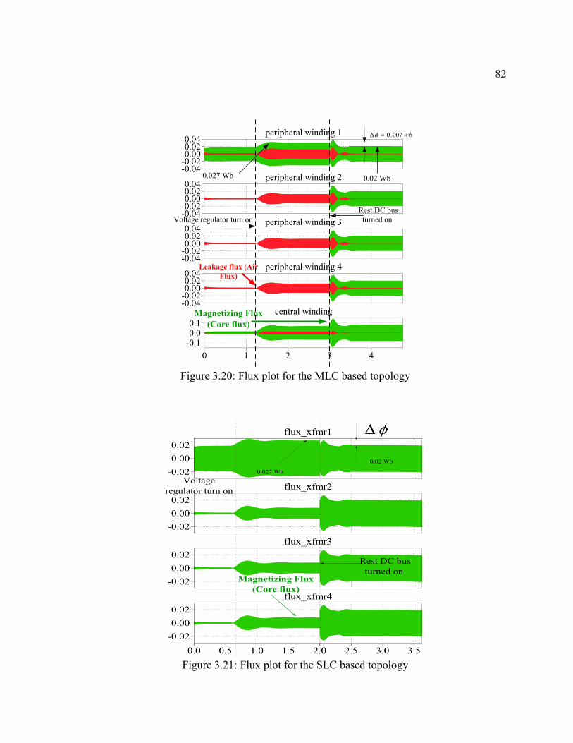
82
Wb007.0
Magnetizing Flux
(Core flux)
Leakage flux (Air
Flux)
Voltage regulator turn on
Rest DC bus
turned on
0.027 Wb 0.02 Wb
Figure 3.20: Flux plot for the MLC based topology
Magnetizing Flux
(Core flux)
Voltage
regulator turn on
Rest DC bus
turned on
0.027 Wb
0.02 Wb
Figure 3.21: Flux plot for the SLC based topology

83
It was seen that the peak flux was 0.027 Weber as well. In this case there were 4 cores in the
SLC and 4 peripheral limbs and 1 central limb in the MLC. The core material required for the
primary winding limbs are same in the SLC and MLC. Let the winding length be l both for
primary and secondary (Fig.3.18). The secondary limb peak flux for the SLC will be same as
the primary limb peak flux since a single magnetic path connects the primary and the secondary
winding. The required cross section for the secondary limb in each of the transformers in the
SLC configuration is 𝐴𝑆𝐿𝐶 =.027
𝐵𝑝𝑒𝑎𝑘 from (3.10) and the volume required is 𝑉𝑆𝐿𝐶 =
.027
𝐵𝑝𝑒𝑎𝑘𝑙. Since
there are four single phase transformers in the SLC configuration, the total volume is 𝑉𝑆𝐿𝐶 =
.027
𝐵𝑝𝑒𝑎𝑘4𝑙. For the MLC configuration the flux linked to the secondary winding in the central
limb is 0.08 Weber. Hence the area of the central limb has to be 𝐴𝑆𝐿𝐶 =.08
𝐵𝑝𝑒𝑎𝑘 from (3.10) and
the total volume of the central limb is 𝑉𝑀𝐿𝐶 =.08
𝐵𝑝𝑒𝑎𝑘𝑙. Since there is only one central limb we
have a gain in volume in the MLC configuration (3.11).
∆𝑉 = 𝑉𝑆𝐿𝐶 − 𝑉𝑀𝐿𝐶 =. 028
𝐵𝑝𝑒𝑎𝑘𝑙 (3.11)
A more generic analysis is as follows:
𝑉𝑜𝑙𝑆𝐿𝐶 =4𝑙𝑉1
4𝑁1𝑓𝑠𝑤𝐵𝑝𝑘+
4𝑙𝑉24𝑁2𝑓𝑠𝑤𝐵𝑝𝑘
(3.12)
𝑉𝑜𝑙𝑀𝐿𝐶 = 3𝑙𝑉1
4𝑁1𝑓𝑠𝑤𝐵𝑝𝑘+
3𝑙𝑉24𝑁2𝑓𝑠𝑤𝐵𝑝𝑘
+𝑙𝑉𝑠𝑒𝑐
4𝑁𝑠𝑒𝑐𝑓𝑠𝑤𝐵𝑝𝑘 (3.13)
∆𝑉𝑜𝑙 =𝑙𝑉1
4𝑁1𝑓𝑠𝑤𝐵𝑝𝑘+
𝑙𝑉24𝑁2𝑓𝑠𝑤𝐵𝑝𝑘
−𝑙𝑉𝑠𝑒𝑐
4𝑁𝑠𝑒𝑐𝑓𝑠𝑤𝐵𝑝𝑘 (3.14)

84
𝑓𝑜𝑟 ∆𝑉𝑜𝑙 ≥ 0 𝑤𝑒 𝑔𝑒𝑡 𝑉1𝑁1+𝑉2𝑁2−𝑉𝑠𝑒𝑐𝑁𝑠𝑒𝑐
≥ 0 (3.15)
Figure 3.22: Three-limb MLC and SLC topology
Therefore it can be seen from (3.15) that by choosing the rated voltages properly we can obtain
a gain in the magnetic core materiel used in the transformer while going to the MLC based
topology from the SLC topology.
3.12. Design of a MLC transformer based on the magnetic stage loss analysis
This section details out a design for the MLC 5-limb core transformer using the ferrite
core from Magnetics-inc, of material F type 0P49925UC.

85
Figure 3.23: B-H characteristic of the core material used for the construction of the MLC
topology (source: http://www.mag-inc.com/products/ferrite-cores/f-material)
The plot of the permeability and the flux density for core in use is shown in Fig. 3.23. The
plots were obtained from the website (www.mag-inc.com) for the ferrite core material F-type.
Figure 3.24: Core loss for the ferrite core material (F) (source: www.mag-
inc.com/products/ferrite-cores/f-material)

86
The switching frequency is 10 KHz and the voltage across the peripheral limbs are 100V. The
central limb core sees a voltage of 400V. The system power is 1KW. The saturation magnetic
flux density for the core used is 0.47 T. The optimum flux density is calculated by minimizing
the total losses in the magnetic stage as per the following analysis:
𝑃𝑡𝑜𝑡𝑎𝑙 𝑙𝑜𝑠𝑠 = 𝑃𝑐𝑜𝑟𝑒 + 𝑃𝑐𝑢 (3.16)
Minimizing the losses w.r.t. the peak flux density ∆𝐵 we get
𝑑𝑃𝑡𝑜𝑡𝑎𝑙 𝑙𝑜𝑠𝑠𝑑(∆𝐵)
=𝑑𝑃𝑐𝑜𝑟𝑒𝑑(∆𝐵)
+𝑑𝑃𝑐𝑢𝑑(∆𝐵)
= 0 𝑜𝑟 𝑑𝑃𝑐𝑜𝑟𝑒𝑑(∆𝐵)
= − 𝑑𝑃𝑐𝑢𝑑(∆𝐵)
(3.17)
This gives the condition for determining the operating peak flux density for the transformer
core. The derivatives of the core power loss and copper loss w.r.t. peak flux density are given
as [16, (15.11), and (15.12)]:
𝑑𝑃𝑐𝑜𝑟𝑒𝑑(∆𝐵)
= 𝛽𝐾𝑓𝑒(∆𝐵)(𝛽−1)𝐴𝐶𝑙𝑚 ,
𝑑𝑃𝑐𝑢𝑑(∆𝐵)
= −2(𝜌𝜗1
2𝐼𝑟𝑚𝑠2
4𝐾𝑢)(𝑀𝐿𝑇
𝑊𝐴𝐴𝐶2) (∆𝐵)
−3 (3.18)
Substituting the derivative values from (3.18) into (3.17) we get the following expression for
the optimum flux density for the core:
∆𝐵 = [𝜌𝜗1
2𝐼𝑟𝑚𝑠2
2𝐾𝑢
𝑀𝐿𝑇
𝑊𝐴𝐴𝑐3𝑙𝑚
1
𝛽𝐾𝑓𝑒]
(1𝛽+2
)
(3.19)
Table 3.2 gives the definition of each of the parameters mentioned in (3.19) and provides the
corresponding values for the used case.

87
Table 3.2: Parameter definition and values required for optimum flux density calculation
Parameter Definition Value
𝜌 Resistivity of the copper
wire
1.724e-6 (Ohm-cm)
𝜗 Volt seconds for the positive
half cycle across the
transformer
0.005 (V-seconds)
𝐼𝑟𝑚𝑠 RMS current through the
transformer windings
3 Amps at steady state
𝑀𝐿𝑇 Mean length per turn for the
wire
15.24 cm
𝐾𝑢 Window fill factor 0.5
𝑊𝐴 Window area for the core 16.1 cm2
𝐴𝑐 Cross sectional area of the
core
.0013 m3
𝑙𝑚 Mean length of the magnetic
path
19.04 cm
𝛽 Steinmetz parameter 2.85
𝐾𝑓𝑒 Frequency dependent core
material constant
24.7
∆𝐵 Peak flux value obtained in
the central or the peripheral
limb
T
Using the values mentioned in table 3.2 in (3.19) the peak flux density for the peripheral
windings in the MLC transformer come out as shown in table 3.3. From (3.10) it is now
possible to calculate the number of windings in each limb (central and peripheral) also
mentioned in table 3.3.

88
Table 3.3: Peak flux and the number of turns obtained for the central and peripheral limb
∆𝐵 N (number of Turns)
Central Limb 0.15 T 25
Peripheral Limb 0.18 T 50
The losses in the magnetic stage of a power converter can be classified into two categories:
Core loss components
Copper loss components
3.12.1. Core loss calculations
The core loss is a manifestation of the hysteresis loss of the magnetic core element and
is a function of the material, the operating frequency and the peak flux density. The losses in
the core can be measured by the Steinmetz equation [26] given by (3.20)
𝑃𝑣 = 𝑘𝑓𝛼𝛽 (3.20)
Here 𝑃𝑣 is the core loss in mW/cm3, the parameters k, α, and β are the Steinmetz parameters
that depends on the magnetic material used, f is the operating frequency in kHz and is the
peak flux density in kG (kilo-Gauss, where 1 Gauss = 10-4 T). However, the equation (3.20) is
the core loss formula where the excitation voltage is sinusoidal in nature. In case of non-
sinusoidal flux waveform the modified Steinmetz equation has been proposed in [26], [27].
𝑃𝑣 =1
𝑇𝑠∫ 𝑘𝑖|
𝑑𝐵
𝑑𝑡
𝑇𝑠
0
|𝛼(∆𝐵)𝛽−𝛼𝑑𝑡 (3.21)
Where the peak to peak flux density is ∆𝐵, 𝑇𝑠 is the switching period and 𝑘𝑖 is given as (3.22)

89
𝑘𝑖 =𝑘
(2𝜋)𝛼−1 ∫ | cos 𝜃|𝛼2𝛽−𝛼𝑑𝜃2𝜋
0
(3.22)
The modified Steinmetz equation the parameters k, α, and β are same as the original Steinmetz
equation (3.21). The power loss per unit volume will be given by the equation (3.22) which
needs to be multiplied by the total core volume to give the total power loss in the core. The
core used in this application is a ferrite core part number: 0P49925UC from Magnetics-inc
shown in Fig 3.25.
Figure 3.25: Core dimensions for the used core 0P49925UC (source: www.mag-inc.com)
The Steinmetz parameters k, α, and β for the core material (F-type) is given in table 3.4.

90
Table 3.4: Steinmetz parameters for the ferrite material “F” (source:
http://fmtt.com/Coreloss2009.pdf)
Frequency Range k α β
𝑓 ≤ 10 𝑘𝐻𝑧 0.79 1.06 2.85
10𝑘𝐻𝑧 ≤ 𝑓 ≤ 100 𝑘𝐻𝑧 0.0717 1.72 2.66
100𝑘𝐻𝑧 ≤ 𝑓 ≤ 500 𝑘𝐻𝑧 0.0573 1.66 2.68
𝑓 ≥ 500 𝑘𝐻𝑧 0.0126 1.88 2.29
The volume of a 5-limb MLC transformer is given as shown in table 3.5.
Table 3.5: Core volume data for the MLC transformer
Section Volume
Peripheral section (C cores,
8 cores in total )
200 cm3 (each), 1600 cm3 (total)
Central limb (I-cores, 4 in
total)
66 cm3 (each), 264 cm3 (total)
Figure 3.26: The waveform showing the voltage and flux plot in the transformer core
Since the core flux wave shape is non-sinusoidal in nature, the modified Steinmetz equation is
used in this case. Since the transformer was designed with a peak flux density of 0.15T, the

91
peak to peak ∆𝐵 in (3.21) is 0.3T. Since the flux wave shape is triangular, the 𝑑𝐵 𝑑𝑡⁄ is a
constant and equals to 0.3 (0.5 ∗ 𝑇𝑠)⁄ where for a 10 kHz system 𝑇𝑠 = 0.0001. Using the
Steinmetz parameters from table 3.2, 𝑘𝑖 is calculated as 0.0511 using (3.22). Using the
information from table 3.3 the core loss was found to be minimum with central winding number
of turns as 50 and peripheral winding number of turns 50. Thus the power loss per unit volume
is calculated as per (3.21) which comes out as 14.8 mW/ cm3 for the central limb and 4.6 mW/
cm3 for the peripheral limbs. Multiplying the volume with the core loss per unit volume, the
total core loss comes out as 11.39 W for a 1kW system. For a similar rated SLC based topology,
the volume breakdown is shown in table 3.6.
Table 3.6: Core volume data for the SLC transformer
Section Volume
Peripheral section (C cores,
8 cores in total )
200cm3 (each), 1600 cm3 (total)
Central limb (I-cores, 8 in
total)
66 cm3 (each), 528 cm3 (total)
Therefore the total volume of the SLC based topology is 2128 cm3. The power per unit volume
for the SLC topology is 4.67 mW/ cm3. Thus the total core loss for the SLC based topology is
9.93 W for a 1 kW system.

92
Table 3.7: Core loss data for the MLC and the SLC transformers
Total System rating Core Loss in MLC Core Loss in SLC
1000W 11.39W 9.93W
3.12.2 Copper loss calculations
The copper losses are a direct function of the r.m.s. current flowing through the windings.
The copper used in the MLC transformer with the core mentioned before is a function of the
number of turns used and the perimeter of the core. The net copper loss is given by:
𝑃𝑐𝑢 = 𝐼𝑟𝑚𝑠2 𝑅𝐴𝐶 (3.23)
Where 𝐼𝑟𝑚𝑠 is the r.m.s. current through the transformer windings.
Table 3.8: Table showing the total resistance of the windings for the MLC transformer with
50 turns both on peripheral winding and 50 turns on the central winding
Length of copper used (cm) Resistance (mOhms) per cm Total winding resistance
(Ohms)
3048 (peripheral) + 1016
(central)
0.311 1.26

93
Figure 3.27: The data sheet for the used Litz wire for the transformer winding (source:
http://www.mwswire.com/pdf_files/mws_tech_book/page16_17_18_19.pdf)
The current can be expressed in the following equation as [9: (6.6),(6.7)] follows.
𝑖(𝜔𝑡 = 0) = −𝑉𝑖𝑛
2𝜔𝐿[(1 −
𝑉𝑜𝑢𝑡
𝑉𝑖𝑛) (𝜋 − 𝜑) + (1 +
𝑉𝑜𝑢𝑡
𝑉𝑖𝑛)𝜑] (3.24)
𝑖(𝜔𝑡 = 𝜑) =𝑉𝑖𝑛
2𝜔𝐿[(1 +
𝑉𝑜𝑢𝑡
𝑉𝑖𝑛)𝜑 + (1 +
𝑉𝑜𝑢𝑡
𝑉𝑖𝑛) (𝜋 − 𝜑)] (3.25)
From (3.24) and (3.25) the r.m.s. current in the peripheral winding and the central winding can
be calculated. The r.m.s. current obtained for the used case MLC-DAB system at rated
condition is shown in table 3.9.

94
Table 3.9: R.M.S. current through the central and peripheral winding of the MLC-DAB at
rated condition
r.m.s. current (central limb)Amps r.m.s. current (peripheral limb)Amps
2.6 Amps 2.6 Amps
Hence the total copper loss using the resistance values from table 3.8 and the r.m.s. current
value in table 3.9 has been calculated as 8.5 W. For a similar rated series connected core
topology the total copper loss can be calculated using the resistance value from table 3.10 and
the r.m.s. current value of 2.6 Amps as 12.8 W.
Table 3.10: Table showing the winding resistance for the series connected core transformer
Length of copper used (cm) Resistance (𝑚𝑂ℎ𝑚𝑠) per cm Total winding resistance
(Ohms)
6096 0.311 1.9
Table 3.11: Total loss for a 1 KW system in the MLC and the series connected case
Topology Core Loss (W) Copper Loss (W) Total Loss (W)
MLC topology 11.4 8.544 19.94
Series connected
topology
10 12.8 32.8
Table 3.11 shows the comparative loss values for the MLC DAB and the series connected
transformer topology with a significant gain in copper loss for the MLC -DAB.

95
3.13. Proximity effect in the windings
The mutual inductances between the primaries have been neglected in the analysis so far.
But with the increase in the number of peripheral limbs the effect of the mutual inductances
become more important as the peripheral limbs come close to each other spatially (Fig.3.28).
An equivalent electrical model for the magnetic stage of the transformer is shown in Fig. 3.29
along with the coupling capacitors that model the mutual inductances of the neighboring
peripheral limbs. The flux linked with the limb PL1 is λ1, the mutual inductance between PL1
and PL2 and PL4 are L12 and L14. The self-inductance (leakage inductance) of the coil is L1. The
current in the limb 1 winding is i1, in limb 2 is i2 and in limb 4, i4. The voltage equation comes
out as follows (3.26):
𝜆𝐿1 = 𝐿1𝑖1 + 𝐿14𝑖4 + 𝐿12𝑖2 , 𝑣1 = 𝑖1𝑅1 + 𝑑𝜆𝐿1 𝑑𝑡⁄ (3.26)
a
a PL1
PL2
PL3
PL4
CL
2a
2a
Proximity effect
Figure 3.28: Top view of the five limb core MLC topology

96
Thus the limb 1 voltage v1 is dependent on the mutual inductances between the neighboring
limbs. The mutual inductances increase with the limbs coming closer. The coupling capacitors
appearing in a five limb core is shown in the Fig. 3.29. For limb PL1 and PL2 the coupling
capacitor is C12, between PL4 and PL1 it is C14 and so on. The coupling is only considered for
the spatially close limbs. No coupling is assumed between the limbs PL1 and PL3. Since the
motivation behind the MLC configuration is the decoupling of the individual primaries, this
mutual coupling is a disadvantage.
1PL
2PL
3PL
CL4PL
12C
23C
14C
34C
Figure 3.29: Electrical equivalent circuit of the MLC topology with the capacitors

97
3.14. Power flow equations in the MLC topology
The power flow equations can be derived from the equivalent circuit of the MLC converter.
Again the three limb core is used for simplification. Similar analysis is valid for a five limb
core model.
Figure 3.30: Electrical equivalent circuit of the three limb core topology with two source and
one load
The equivalent circuit for the three limb core is shown in Fig. 3.30. Vo & V1 are the primary
voltages while V2 is the secondary voltage, and L1 + L2 is the lumped sum of the winding
inductances all three taken together. The current in the circuit can be derived as (3.27):
Lj
VVVI L
22110 (3.27)
L
VV
L
VV
L
VVP o
221
0
1112211
sinsinsin
1
(3.28)

98
L
VVV
L
VV
L
VVP o
2201
0
2221212
sinsinsin
1
(3.29)
𝑃1 is the power injected by source 2 to the load and 𝑃2 is the summation of power injected by
source 1 & 2 to the load. In the derivation 𝛿1 (relative phase shift between source 1 & 2) is
made zero. Thus, both the two sources are in same phase which reduces real power flow
between the primaries. Power flow between the primaries and the secondary hence depends
solely on the secondary phase angle 𝛿2.The power angle graph is given in Fig. 3.37 based on
(3.28) and (3.29). The maximum is at 𝛿2 =𝜋
2. Similar argument can be extended to the five
limb core topology. Provided all the primary bridges are in phase, the power angle curve will
be similar as that in Fig. 3.27.
3.15. A small signal model for the MLC-based DAB converter for analyzing the
parameter sensitivity
The electrical equivalent circuit for the MLC based DAB topology is shown in Fig. 3.32.
Since the primary sources are connected in series and the same current (winding current) flows
through all the sources, the MLC based DAB topology can be simplifies to a simple DAB
topology to study the system dynamics and derive the small signal model. The small signal
model for a single phase DAB has been derived in [9]. The small signal model and the transfer
functions for the MLC based DAB is derived based on the single phase DAB. Identifying the
state variables as the output capacitor voltage and the inductor current, the state space equations
for the average model of the DAB [9,(6.17)] is given in (3.30).

99
[ 𝐼
] = [
02𝑘1 − 1
𝐿1
𝐶−1
𝑅𝐶
] [𝐼𝑉] + [
2𝑘 − 1
𝐿0
]𝑉 𝑖𝑛 (3.30)
The expression 𝑘1 and 𝑘 can be expressed [9, (6.13), (6.14)] as per (3.31)
𝑘1 =2𝜑 + (
𝑉𝑜𝑢𝑡𝑉𝑖𝑛
− 1)𝜋
4𝜋(1 +𝑉𝑜𝑢𝑡𝑉𝑖𝑛) 𝑎𝑛𝑑 𝑘 = 𝑘1 +
1
2 (1 −
𝜑
𝜋) (3.31)
In (3.30) L is the leakage inductance of the transformer, C is the output capacitor, R is the load,
I is the leakage inductor current or the winding current and 𝑉 is the output capacitor voltage.
Linearizing the average model provides the small signal model [9, (6.18)-(6.21)].
[ 𝑑𝐼
𝑑𝑡𝑑
𝑑𝑡 ]
= [𝐴11 𝐴12𝐴21 𝐴22
] [ 𝐼] + [
𝐵110]𝑉𝑖 + [
𝐸110] (3.32)
𝐴11 = −2𝑉𝑖𝑛0
𝑇𝑠(𝑉𝑖𝑛0 + 𝑉0) (3.33)
𝐴12 =1
2(𝑉𝑖𝑛0𝑇𝑠((𝜑0 − 3𝜋)𝑉𝑖𝑛0 − 2𝑉0𝜋) + 4𝜋𝐿𝐼0𝑉𝑖𝑛0 − 𝜋𝑇𝑠𝑉0
2
𝜋𝑇𝑠𝐿(𝑉𝑖𝑛0 + 𝑉0)2) (3.34)
𝐵11 =𝑉0(𝑇𝑠𝜑0𝑉0 − 2𝜋𝐿𝐼0) + 𝜋𝑇𝑠𝑉𝑖𝑛0(𝑉𝑖𝑛0 + 2𝑉0)
𝜋𝑇𝑠𝐿(𝑉𝑖𝑛0 + 𝑉0)2 (3.35)
𝐸11 =𝑉0
𝜋𝐿 (𝑉0𝑉𝑖𝑛0
+ 1) (3.36)

100
For the used case transformer the parameters and their values are provided in table 3.8. The
control to output transfer function can now be derived [9, (6.22) – (6.25)] as shown.
𝐺𝑣𝑑(𝑠) =𝐼(𝑠)
𝜑(𝑠)|𝑢(𝑠)=0
(3.37)
𝐺𝑣𝑑(𝑠) =𝑁𝑢𝑚(𝑠)
𝐷𝑒𝑛(𝑠) (3.38)
Table 3.12: MLC-DAB converter parameters
Parameters Value Representation
𝑉𝑖𝑛0 400V Steady State input voltage
𝑉0 400V Steady State output voltage
𝜑0 𝜋
6
Steady State Power angle
L 0.7 mH Lumped leakage inductance of the
transformer
𝐼0 2.5 Amp Average inductor current over one
switching half-cycle
𝑇𝑠 100µs Switching period
Where 𝑁𝑢𝑚(𝑠) and 𝐷𝑒𝑛(𝑠) are the numerator and denominator of the transfer function.
𝑁𝑢𝑚(𝑠) =𝐸11𝐶 (3.39)
𝐷𝑒𝑛(𝑠) = 𝑠2 + 𝑠 (1
𝑅𝐶− 𝐴11) −
𝐴11𝑅𝐶
−𝐴12𝐶 (3.40)

101
3.16.1. Transformer leakage inductor sensitivity analysis for open loop system
The transfer function 𝐺𝑣𝑑(𝑠) is dependent on the value of the inductor (leakage
inductance) of the transformer, since the parameter 𝐴12 in the denominator is a function of the
leakage inductance. Fig. 3.31 shows the bode plot of the transfer 𝐺𝑣𝑑(𝑠) showing the change
in the phase margin of the open loop system with the change in the leakage inductance of the
transformer. Table 3.13 shows the trend variation of the phase margin with the leakage
inductance.
L –
decreasing
Figure 3.31: Bode plot for the control to output transfer function 𝐺𝑣𝑑(𝑠) showing the
variation in phase margin with leakage inductance
The denominator of the transfer function (3.34) can be written as
𝐷𝑒𝑛(𝑠) = 𝑠2 + 𝐵𝑠 − 𝐶 (3.41)

102
Where B and C are:
𝐵 =1
𝑅𝐶− 𝐴11, 𝐶 = [
𝐴11
𝑅𝐶+𝐴12
𝐶]. Thus only C is a function of the leakage inductance. The poles
𝑝𝐺𝑣𝑑 of the transfer function are therefore,
𝑝𝐺𝑣𝑑 = −𝐵
2± √
𝐵2
4+ 𝐶 (3.42)
Now to obtain the sensitivity of the poles with the variation in L, (3.42) is partially
differentiated w.r.t. L.
𝜕𝑝𝐺𝑣𝑑𝜕𝐿
=
𝜕 [−𝐵2 ±
√𝐵2
4 + 𝐶]
𝜕𝐿=
𝜕 [√𝐵2
4 + 𝐶]
𝜕𝐿= 0 (3.43)
This criterion leads to
𝜕𝐶
𝜕𝐿= 0 𝑠𝑢𝑏𝑠𝑡𝑖𝑡𝑢𝑡𝑖𝑛𝑔,
𝜕𝐴12
𝜕𝐿= 0 (3.44)
This leads to the following criterion
𝑉𝑖𝑛0𝑇𝑠((𝜑0 − 3𝜋)𝑉𝑖𝑛0 − 2𝑉0𝜋) − 𝜋𝑇𝑠𝑉02 = 0
Substituting 𝑉0 = 𝑚𝑉𝑖𝑛0, we get
𝜑0 = 𝜋(𝑚 + 1)2 + 2𝜋 (3.45)
However since max(𝜑0) =𝜋
2 hence clearly (3.45) is invalid, which proves that the open loop
system cannot be made insensitive of L.

103
Table 3.13: Leakage inductance dependence on the system stability
Leakage
inductance
Phase margin Settling time Percentage
Overshoot
0.1 mH 11.9 o 0.8msec 11%
0.3 mH 20.4 o 1.8msec 0
0.7 mH 30.7 o 5msec 0
1mH 36.3 o 7msec 0
3mH 57.6 o 22.5msec 0
In the following subsection an inner current loop controller design is presented that improves
the operation of the close loop system with the variation of L.
3.16.2. Design of a Compensator for improving the variation in stability due to variation
in L
In the previous section it was shown that the open loop system is sensitive of L. The
variation in L has an impact on the system stability (table 3.13). In this section a control method
is proposed that improves the system stability by improving the gain margin with the variation
in L. The closed loop poles of the system is shown in equation (3.42). Since the poles are
function of the L, variation in L will affect the variation in the pole location and hence the
system stability. Since the poles occur in conjugate pair with one pole closer to the origin while
the other further away, the pole closer to the origin will have a greater effect on the system
stability. This provided the motivation of implementing a compensator that cancels the
dominant pole closer to the origin with its zero. Fig 3.32 shows the proposed controller.

104
Compensator Plant (MLC-DAB)
Figure 3.32: Compensator designed to compensate for the variation in L
The controller parameter can be designed by identifying the pole closer to the origin.
𝑇 =1
𝑝𝑔𝑣1, 𝑖𝑓 𝑝𝑔𝑣
1 < 𝑝𝑔𝑣2 (3.46)
the compensator transfer function 𝐶𝑜𝑚𝑝(𝑠) with the above design is as:
𝐶𝑜𝑚𝑝(𝑠) = .05 [1 + 𝑠 1200⁄𝑠1200⁄
] (3.47)
The variation in L and the consequent effect on the controller stability is shown with the
example case in Fig. 3.35. The phase margin variation is shown in table 3.14.
Table 3.14: Table showing the phase margin w.r.t change in L
Leakage Inductance
(mH)
Phase Margin(degrees)
3 53.6
1 78.5
.7 86.8
.5 93.7
.1 111

105
The sensitivity coefficient of the open loop and closed loop transfer function are calculated in
the following section.
L-
decreasing
Figure 3.33: Variation of the phase margin and stability of the closed loop system with the
compensator with the variation in the leakage inductance (L) of the transformer.
3.16.3. Evaluation of transfer function sensitivity coefficient:
The transfer function sensitivity coefficient w.r.t. change in L for the open loop system
is represented as follows:

106
𝑆𝑜𝑙 =
𝜕𝐺𝑣𝑑𝐺𝑣𝑑𝜕𝐿𝐿
=𝜕𝐺𝑣𝑑𝜕𝐿
𝐿
𝐺𝑣𝑑 (3.48)
Since 𝐺𝑣𝑑 =𝑁𝑢𝑚(𝑠)
𝐷𝑒𝑛(𝑠), (3.48) can be simplified as follows:
𝑆𝑜𝑙 = 𝐿 [1
𝑁𝑢𝑚
𝜕𝑁𝑢𝑚
𝜕𝐿−
1
𝐷𝑒𝑛
𝜕𝐷𝑒𝑛
𝜕𝐿] (3.49)
Substituting from (3.48) and (3.49), the open loop sensitivity function can be expressed as
follows:
𝑆𝑜𝑙 = −1 −𝐿
𝐷𝑒𝑛(𝑠)[𝑉𝑖𝑛0[(𝜑0 − 3𝜋)𝑉𝑖𝑛0 − 2𝑉0𝜋] − 𝜋𝑉0
2
2𝐶𝜋(𝑉𝑖𝑛𝑜 + 𝑉0)2] (3.50)
The close loop sensitivity coefficient with the changes in the forward transfer function can be
evaluated as follows:
𝑆𝑐𝑙 =
𝜕𝑇(𝑠)𝑇(𝑠)⁄
𝜕𝐺𝑣𝑑(𝑠)𝐺𝑣𝑑(𝑠)⁄
=𝜕
𝜕𝐺𝑣𝑑(𝑠)[𝐺𝑣𝑑(𝑠)𝐶𝑜𝑚𝑝(𝑠)
1 + 𝐺𝑣𝑑(𝑠)𝐶𝑜𝑚𝑝(𝑠)] .
𝐺𝑣𝑑(𝑠)
[𝐺𝑣𝑑(𝑠)𝐶𝑜𝑚𝑝(𝑠)
1 + 𝐺𝑣𝑑(𝑠)𝐶𝑜𝑚𝑝(𝑠)]
=1
1 + 𝐺𝑣𝑑(𝑠)𝐶𝑜𝑚𝑝(𝑠) (3.51)
Where 𝑇(𝑠) is the closed loop transfer function, 𝐶𝑜𝑚𝑝(𝑠) is the compensator transfer function
from (3.47), and 𝐺𝑣𝑑(𝑠) is the open loop system transfer function from (3.37). The open loop
sensitivity coefficient and the closed loop sensitivity coefficient are plotted in Fig. 3.34. With
the addition of the compensator the sensitivity coefficient shows better attenuation throughout
the frequency range.

107
Sensitivity (with
compensation)
Sensitivity (without
compensation)
Figure 3.34: Sensitivity coefficient plot for the open loop system (green) and the closed loop
system (blue) showing better attenuation of the sensitivity under closed loop operation
3.16.4. Effect of wide variation in input voltage on the converter transfer function
Since the motivation of implementing the MLC-DAB was to integrate RES with
fluctuating power profile, it is important to analyze the impact of input voltage swing on the
converter source to output transfer function. The source to output transfer function as derived
in [9, (6.29)] is given as (3.52).
𝐺𝑣𝑔(𝑠) =𝑉(𝑠)
𝑉𝑖𝑛(𝑠)=𝑁𝑣𝑔(𝑠)
𝐷𝑖𝑛(𝑠), 𝑤ℎ𝑒𝑟𝑒, 𝑁𝑣𝑔(𝑠) =
𝐵11𝐶 (3.52)
The variation in phase margin of 𝐺𝑣𝑔(𝑠) with the variation in input voltage 𝑉𝑖𝑛𝑜 is shown in
table 3.15.

108
Table 3.15: Variation in the phase margin of source to output transfer function with the
variation in source voltage
Input Voltage (V) Phase margin (degrees)
50 87.8
100 133
200 138
400 144
600 152
800 160
From table 3.15 it is clear that with the change in source voltage the system has significant
phase margin and hence the system is stable. Fig. 3.35 shows the magnitude and phase plot for
the 𝐺𝑣𝑔(𝑠) transfer function showing the phase margin under different input voltage
conditions. However the variation in the control to output transfer function is more sensitive
on the input voltage swing. Table 3.16 shows the variation in phase margin w.r.t. the input
voltage variation on the 𝐺𝑣𝑑(𝑠). Since the system goes out of stability with the decrease in the
input voltage, this provides the motivation for integrating a storage element in the system that
provides support during the source voltage fluctuations. The following section discusses the
storage (battery) integration and output power (or voltage) regulation algorithm.
Table 3.16: Variation in phase margin for the control to output transfer function
Input Voltage (V) Phase margin (degrees)
50 9.53
100 18
200 32
400 52
600 64
800 75.1
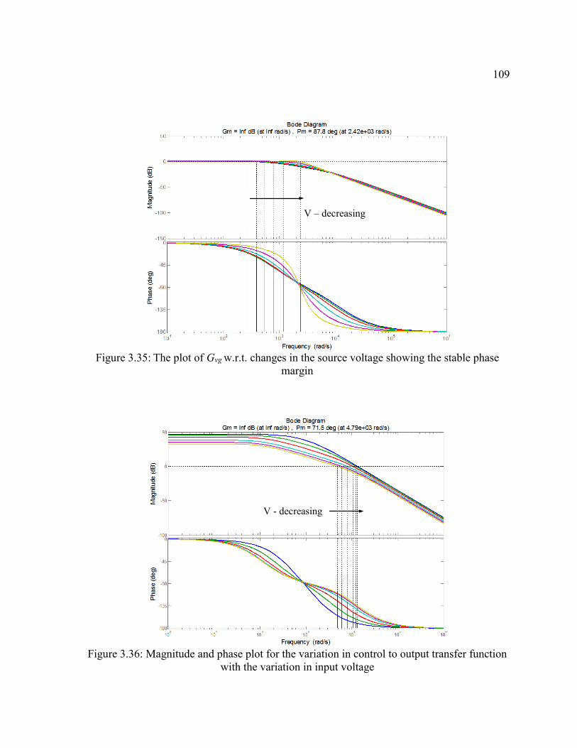
109
V – decreasing
Figure 3.35: The plot of Gvg w.r.t. changes in the source voltage showing the stable phase
margin
V - decreasing
Figure 3.36: Magnitude and phase plot for the variation in control to output transfer function
with the variation in input voltage

110
3.16. Power smoothing algorithm using energy storage:
Since the motivation of implementing the MLC-DAB was to integrate RES with
fluctuating power profile, a power smoothening algorithm has been proposed in this section.
This algorithm uses a storage element to act as an energy buffer while supplying a regulated
load. A five limb core MLC topology was considered and one of the peripheral limbs was
connected to a battery bank. Two distinct modes of the converter are defined based on the role
played by the battery storage element. The accumulator mode is where the battery acts as a
source and the distributor mode is where the battery is charged at a constant current. The
secondary phase shift angle 𝛿2 is observed. If the angle goes below a certain lower threshold
then the converter switches over to the distribution mode i.e. the battery is charged. This is
achieved by phase lagging the H-bridge connected to the battery with respect to the other
primaries. As a result the load increases and the operating power angle increases as well. In
the distributor mode if the operating angle keeps on increasing and hit a maximum the
controller then switches over to accumulator mode. The battery now supplies the load by
syncing up with the other primaries. Thus the converter always operates within the
angle[𝜑𝑚𝑎𝑥, 𝜑𝑚𝑖𝑛]. Fig. 3.37 explains the process with respect to the power angle curve. The
converter will go into accumulator mode when the battery charging current reaches a maximum
value. If a precise control of the charging or the discharging current is needed one might
implement the duty cycle modulation for input current control explained in previous sections.
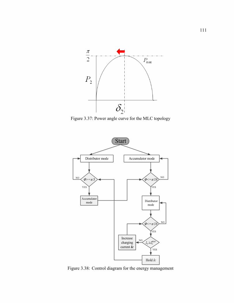
111
Figure 3.37: Power angle curve for the MLC topology
Start
Φ>=π/3 Φ<=π/18
Accumulator mode Distributor mode
NO NO
Accumulator
mode Distributor
mode
YES YES
Φ<=π/18NO
YES
Increase
charging
current IcYES
NO
Hold Ic
Figure 3.38: Control diagram for the energy management

112
Figure 3.39: Energy management algorithm from the power angle perspective
3.17. Experimental results:
The lab setup is shown in Fig 3.40. The MLC transformer has five limbs; the peripheral
limbs are attached to regulated dc power sources. One of the limb is attached to a motor-
generator coupled system that implements wave energy with widely varying DC bus voltage.
A battery pack is attached to one of the limbs that supplied current when the available power
is low and takes in current in case of excess (Fig. 3.41) thus maintaining a regulated dc bus at
the output. Figure 3.42 shows the MLC transformer with five limbs. The mechanical structure
is three dimensional and hence requires support frames to build. Ferrite was chosen for the
core material and litz wires for the winding. Fig. 3.43shows the terminal voltages for the MLC
transformer.
113
Generator
MLC
transformer
Battery pack
Figure 3.40: Lab setup for the MLC topology with the motor generator setup acting as a wave
energy simulator
Unregulated DC bus from
wave energy source
Output DC bus
Regulated
Battery
Current
Charging
Discharging
Figure 3.41: Experimental result showing the MLC regulating a DC bus with the wave
energy and battery integrated
114
Figure 3.42: The five limb MLC transformer.
Figure 3.43: Terminal voltage waveforms for the five limb MLC transformer

115
The input current control operation has been demonstrated with experimental results as shown
in Fig. 3.44. Duty cycle modulation was implemented on the primary H-bridges to regulate the
current while the input DC bus voltage was changed. The current controller kept the current at
the desired set point (one source at 0.8 amps and another at 0.5 amps).
Figure 3.44: Control diagram for the input current control operation on the 3 limb MLC
topology
Battery
Bridge 2RES
Bridge 1
Secondary
(lagging) bridge
Unregulated DC
bus
Bridge 3
PI
I source1
Iref1
I source2
Iref2
50%
duty
cycle
PWM
waveformPI
116
0.5Amps
regulated
0.8Amps
regulated
50 V from battery
Unregulated Source
(60V to 120 V)
0.5Amps
regulated
0.8Amps
regulated
50 V from battery
Unregulated Source
(60V to 120 V)
Figure 3.45: Experimental results for the three-limb MLC topology with input current control
3.18. Conclusions
In this chapter a multi-terminal DAB (MLC-DAB) converter topology was developed
using a multi-limb core (MLC) transformer. The MLC topology shows an alternate approach
to the multi – input single output DC to DC converter system with isolation. The main results
obtained in this chapter are summarized as follows:
In this chapter the MLC transformer based DAB was proposed and the equivalent
electrical circuit was developed using the gyrator concept.

117
The MLC-DAB topology was shown to utilize reduced copper and magnetic core
material compared to an electrically equivalent series connected multi-terminal
DAB topology.
A PWM based input current control was developed to integrate different renewable
energy sources operating at different maximum power point.
A small signal analysis of the MLC-based DAB was done using the DAB small
signal as the base model. The sensitivity analysis of the converter dynamics was
shown w.r.t. the leakage inductance of the transformer. A controller was
implemented to improve the sensitivity of the converter w.r.t. L variations.
A loss calculation was done for the MLC transformer and compared with the
competing series connected transformer topology. In terms of core loss and copper
loss the MLC based topology was shown to have lower losses compared to the
series connected transformer topology.
A power smoothing algorithm was proposed. A fluctuating power source and a
battery was integrated to supply a regulated load verifying the power smoothening
algorithm.
In the next chapter of the dissertation the MLC-DAB has been applied to the solid state
transformer topology for grid integration of multiple renewable energy sources.

118
Chapter 4 The solid state transformer application of the Dual
Active Bridge converter
4.1. Introduction
The dual active bridge (DAB) converter and the MLC-DAB converter discussed in the
previous chapters find various applications, such as traction, renewable energy integration, etc.
One of the application is the DC to DC stage of the Solid State Transformer topology. In this
chapter the solid state transformer (SST) application of the MLC-DAB is the main focus of
discussion. Instead of the conventional transformer where the magnetic isolation is provided
at 60 Hz, the solid state transformer topology proposes the isolation at high frequency [1], [2]
reducing the overall size and weight. To obtain high frequency in the SST topology, the 60 Hz
AC is rectified through an active front end and converted to DC. The DC to DC stage provides
the isolation through the DAB converter. Several different topologies have been proposed for
the SST topology with the DAB converter. For higher voltage applications a cascaded front
end based topology have been proposed in [2], [21]. For three phase application a three phase
front end have been proposed with a three phase DAB stage in [28], [29], [30]. In this chapter
is a single phase solid state transformer topology have been considered for the integration of
the MLC-DAB as the DC – DC stage. The advantages of integrating the MLC-DAB into the
SST topology has been shown compared to DAB integration. A startup algorithm for the SST
has been proposed to reduce inrush currents. A parallel MLC-DAB based SST test bed was
developed to form a micro-grid and a black start algorithm was implemented to restore power

119
under islanding. The critical load points were identified within the micro-grid and
uninterrupted power flow was demonstrated under islanding.
4.2. Single phase SST cascaded topology
The single phase cascaded SST topology is shown in Fig. 4.1.
Input Rectifier DC to DC stage
Input Inductor
RES
Storage
HF
transformer
HF
transformer
HF
transformer
Output
Inverter
Figure 4.1: Single phase SST topology with cascaded front end and DAB for the DC to DC
stages
The cascaded series connected front end converter produces a seven level voltage waveform
to block the medium voltage ac bus in the input. This produces three DC buses that need to be
balanced. Balancing of the DC buses are assigned both to the input rectifier stage as well as

120
the DC to DC stage which in this case is the Dual Active Bridge converter. The following
section discusses the controls for the front end stage along with the voltage balance control.
4.3. Voltage balance control of the SST
The active front end controls have been extensively discussed in [1] and [31]. Fig. 4.2
shows the block diagram for the control of the front end.
PI
Saturation to 2 p.u.
PI
d-axis controller
d-axis controller
PI
q-axis controller Inverse d-q
Figure 4.2: Vector Control of the active front end converter
The d-axes control the DC bus of the front end while the q-axes maintain the unity power factor
operation. The outer voltage loop maintains the overall DC bus i.e. the sum of the DC bus. For
individual DC bus control the additional voltage balance loop is required as shown in Fig. 4.3.
This control observes each individual DC buses and adjusts the d-axes modulation required to
maintain the balance. The d – axes modulation for the rectifier bridge 1 is given as(𝑚𝑑 + ∆𝑚1)
for bridge 2 is given as (𝑚𝑑 + ∆𝑚2) and for bridge 3 is given as(𝑚𝑑 − ∆𝑚1 − ∆𝑚2). The

121
third bridge doesnot have its own controller. In case of voltage sag the power goes below 1
p.u. the buses 1 and 2 maintain the rated voltage while the rest is on bus 3. Considering the
voltages are balanced and the output dc bus voltages are gives as E. The rectifier terminal
voltages are V1, V2, V3 respectively. The power transferred by each bridge are P1, P2, P3 and
the modulation index in d-axes is given by m1, m2, m3 .
𝑉1 = 𝐸(𝑚1 + 𝑗𝑞1), 𝑉2 = 𝐸(𝑚2 + 𝑗𝑞2), 𝑉3 = 𝐸(𝑚3 + 𝑗𝑞3) (4.1)
𝑉1 + 𝑉2 + 𝑉3 = 𝑉𝑙𝑖𝑛𝑒 − 𝑗𝜔𝐿𝐼𝑙𝑖𝑛𝑒 (4.2)
𝑃1 = 𝐼𝑙𝑖𝑛𝑒𝑚1𝐸 , 𝑃2 = 𝐼𝑙𝑖𝑛𝑒𝑚2𝐸 , 𝑃3 = 𝐼𝑙𝑖𝑛𝑒𝑚3𝐸 (4.3)
𝑃1𝐷𝐴𝐵 =
𝑉𝑖𝑛𝑉𝑜𝑢𝑡𝜔𝐿
𝜑1 (1 −𝜑1𝜋) , 𝑃2
𝐷𝐴𝐵 =𝑉𝑖𝑛𝑉𝑜𝑢𝑡𝜔𝐿
𝜑2 (1 −𝜑2𝜋) , 𝑃3
𝐷𝐴𝐵 =𝑉𝑖𝑛𝑉𝑜𝑢𝑡𝜔𝐿
𝜑3 (1 −𝜑3𝜋)
(4.4)
The power transferred by DAB are given by (4.4) where 𝑃1𝐷𝐴𝐵, 𝑃2
𝐷𝐴𝐵 𝑎𝑛𝑑 𝑃3𝐷𝐴𝐵 are the power
transferred by the DAB with leakage 𝐿1, 𝐿2and 𝐿3. Under voltage sag when Pin = Pnominal the
power transferred by each DAB is one third of Pnominal . Under these situation no further control
modifications is not required on the DAB side. If however under voltage sag Pin < Pnominal in
that case the 𝑃1𝐷𝐴𝐵 = 𝑃2
𝐷𝐴𝐵 =1
3𝑃𝑛𝑜𝑚𝑖𝑛𝑎𝑙 and 𝑃3
𝐷𝐴𝐵 = 𝑃𝑖𝑛 −2
3𝑃𝑛𝑜𝑚𝑖𝑛𝑎𝑙. Depending on how
much severe the voltage sag is the power transferred by the third DAB maybe zero. The phase
shift angles are under such circumstances 𝜑1 = 𝜑2 = 𝜑3 =𝜋
2. Since DAB1 and DAB 2 has
input buses with voltage in them will transfer maximum power and will be heavily loaded. The
122
current through them will be the maximum. Since the voltage in input bus for DAB3 is below
nominal rated value, DAB3 will be under rated load. This is not a desirable condition. We need
the DAB to be equally balanced. Hence to avoid this condition, under severe voltage sag the
rectifier output DC buses need to be brought down to a value that all the three buses can be
balanced. Figure 4.7 shows the rectifier buses balance out even after 0.3 p.u. voltage sag by
reducing the reference voltage to 0.6 p.u. This affects the DAB as the currents are now balanced
and the power sharing is equal.
PI Rectifier
Bridge 1
PI Rectifier
Bridge 2
Rectifier
Bridge 3 +
--
Figure 4.3: DC voltage balance control for the front end
123
Voltage PI DAB1Σ
Vref
Vout
Current PIIref
Current PI
Σ
Σ
IDAB2
DAB2
Current PIΣ
IDAB3
DAB2
IDAB1
Figure 4.4: Power balance in the DAB stage
Sag
Voltage Sag
(0.6 p.u.)
Figure 4.5: Simulation results with a voltage sag of 0.6 p.u. with the DC bus regulation intact
124
Voltage Sag
Voltage Sag
Figure 4.6 Input voltage sag of 0.3 p.u. with the DC bus collapse
Figure 4.7: A 0.3 p.u. voltage sag with modified DAB power balance control to maintain DC
bus balance

125
Fig. 4.4 shows the power balance control on the DAB stage under steady state operation. The
outer voltage loop provides a current reference 𝐼𝑟𝑒𝑓 to the inner current loops. The measured
current from each DAB is the high frequency inductor current sampled in a moving window
fashion. Phase shift angle is generated for each DAB as the output of the current loop (Fig.
4.4). If the leakage inductance of the HF transformer of the individual DAB are different, the
power transferred will be different as well (4.4). Hence the inner current loop maintains the
power balance by providing the same average current reference. The power angle curve in Fig.
4.8 explains the power balance.
Pow
er
Phase Shift Angle
Figure 4.8: Power angle curve for the DAB with different leakage inductors and operating at
different phase shift angles to transfer the same power

126
4.4. Inrush current limit at startup
The cascaded solid state transformer topology (Fig. 4.1) has three DC bus capacitors.
Hence during startup there will be inrush current that might damage the front end switches. To
limit the inrush current at start up a soft start algorithm is proposed in this section. In order to
implement a soft start the DAB output bus is connected to an auxiliary dc source or a storage
device. Considering the SST is disconnected from the grid this source charges up the rectifier
buses. This is possible since DAB is a bidirectional DC to DC converter. The rectifier bridges
will be switching under this condition as an inverter with the voltage reference from the PLL
connected to the grid voltage. When the rectifier DC buses have reached a nominal rated
voltage level the breaker is turned on connecting the grid to the rectifier. The rectifier changes
over from inverter to rectification mode and regulates the DC bus. The auxiliary DC supply is
disconnected or changes over to power absorbing mode and the power flows into the inverter
to the load at its output. Adopting this method the inrush current is completely avoided and the
start-up current is limited to 2 p.u. This is because neither the rectifier not the DAB sees an
discharged DC bus while the power flow actually takes place. Fig. 4.9 shows the simulation
results of the startup scheme described before. The current does not go beyond 1 p.u. and
reaches steady state.

127
START SIGNAL
Inverter
Rectifier
Grid Connected
Grid Disconnected
Charging from DC source
Figure 4.9: Soft Start of the SST from the auxiliary power supply
Table 4.1: Soft Start algorithm
4.5. Single phase SST topology with the MLC –DAB topology:
In this section of the chapter an alternate topology is proposed in the DC to DC stage of
the SST. The MLC-DAB topology proposed in the previous chapter has been used to replace
the parallel DAB stages as shown in Fig. 4.10. The MLC-DAB topology has several
Stage Function
1 Startup is initiated from the LV side DC bus i.e. a battery bank or
DRES
2 The DC stage charges up the rectifier side DC capacitor.
3 The rectifier works as inverter with 𝐼𝑑 = 0 &𝐼𝑞 = 0.
4 When the dc bus capacitors reach nominal rated value the grid breaker
is turned on.
5 The rectifier gains control of the dc bus and the power flow direction
for the DC stage is reversed.

128
advantages in terms of reduction in magnetic material, copper and silicon area. The number of
H-bridges is reduced on the secondary side since there is only one secondary winding. Battery
or any other auxiliary DC source is directly connected to the transformer through an H-bridge,
instead of being connected to the DC bus as in Fig. 4.10. The secondary bridge is connected to
the central limb of the MLC and the primaries are connected to the peripheral limbs (Fig. 4.10).
The central limb acts as an accumulator of flux from all the other limbs of the transformer. The
primaries are all synchronized and switched at 50% duty cycle without any relative phase shift
between them. Power transfer takes place by phase shifting the secondary with respect to the
primary. A test bed of the MLC topology has been built as shown in Figure 4.12. The MLC-
DAB based topology gives the advantage that we do not need to balance the dc bus voltage.
Nor there is any requirement for power balance in the dc to dc stage. The reason is because the
current in all the windings are same and hence same current flows through all the input
terminals. The mismatch of the leakage inductance associated with each winding doesn’t affect
the power balance, since all the leakages add up in series.
129
V in
MLC Transformer
Input
Voltage
Input
Inductor
Auxiliary DC
source
Output
Inverter
Figure 4.10: Single phase SST with the MLC transformer
Figure 4.11: The voltage sag simulated with a MLC topology based SST without using any
voltage bus balance control in the DC to DC stage as well as the front end stage

130
Active
front end
MLC based DC
to DC stage
Figure 4.12: Experimental setup in the lab
4.6. Experimental results of the single phase SST topology showing the soft start
and the MLC-DAB integration:
The experimental setup was developed in the lab as shown in Fig. 4.12. The parallel DAB
based topology was developed first and the soft start algorithm was implemented as was
discussed in section 4.4. Fig. 4.13 and Fig. 4.14 shows the experimental result of the soft start
algorithm.

131
Figure 4.13: Soft start algorithm (DC side waveforms)
Figure 4.14: Soft start algorithm (AC side waveforms)
132
Fig. 4.13 shows the DC buses on the DAB input buses rising gradually as commanded by the
controller. There is an inrush current still on the DAB stage. This comes from the auxiliary
source connected to the output of the DAB DC bus. Further reduction in this current can be
obtained if duty cycle modulation is done on the primary side of the DAB. Fig. 4.15 shows the
steady state results of the MLC based SST topology as shown in Fig. 4.10. There is no voltage
balancing loop in this case with the active front end. Fig. 4.16 shows the situation with voltage
sag implemented in the MLC-SST. It is seen that the line current increases to provide the
voltage regulation on the DC buses.
DC bus voltages
PWM rectifier voltage
DC bus voltages
Line current
Figure 4.15: Steady state operation of the MLC based SST topology

133
Line current
DC bus voltages
Input AC voltage sag
Line current
DC bus voltages
Startup transient (without DC bus balance)
Figure 4.16: Experimental results showing the voltage sag compensation without the voltage
bus balancing control (left). The right shows the startup pf the SST with the inrush current
but without any voltage bus control
4.7. The renewable energy hub concept
The renewable energy hub (REH) concept is shown in Fig. 4.17. It is an extension of the
solid state transformer concept with multiple renewable energy source (RES) integrations. In
the solid state transformer the renewable energy integration takes place in the output DC bus
of the DAB converter as shown in Fig. 4.18. Individual RES are tied to a common DC bus
through an isolated DC to DC converter forming the local DC micro-grid. Parallel connection
of these DC to DC converters require power balancing algorithms to be implemented on these
converters. Several DC droop based control algorithms have been proposed [3], [11].
134
MLC (multi limb core )Transformer
Grid Side
RES
Output
Inverter
RES
RES
Figure 4.17: The renewable energy hub concept.
Vin
Input Rectifier DC to DC stage
Input Inductor
RES
Storage
Interfacing Converter
Local DC Micro-grid
HF
transformer
HF
transformer
HF
transformer
Figure 4.18: The single phase SST with the DC micro-grid concept.

135
However in the renewable energy hub concept as proposed in Fig. 4.17, the energy is
accumulated in the central limb of the MLC transformer. Loss of modularity is a disadvantage
in this topology but this gives easier control since no power sharing algorithm is required. Input
current driven MPPT can be implemented as discussed in section 3.7 of chapter 3 using duty
cycle modulation. Fig. 4.19 shows the control diagram in the MLC stage of the Renewable
Energy Hub. In case there are multiple RES with multiple MPPT points it is possible to achieve
individual current control for different operating points of individual RES connected to
individual limbs. Considering the case where there are n RES and the current reference
generated from the MPPT be 𝐼𝑘𝑟𝑒𝑓 where 𝑘 = 1,2, … 𝑛. A sorting algorithm determines the
maximum of these current references. The phase shift angle is set by the 𝐼𝑀𝐴𝑋𝑟𝑒𝑓
. The rest of the
current references are attained by the PWM based duty cycle modulation as mentioned in
sectioned 3.7. Fig. 4.20 and Fig. 4.21 shows the simulation results of the MPPT based current
control for RES operation. There are four RES and the maximum is 𝐼𝑟𝑒𝑓 = 10𝐴. This
determines the phase shift between the primaries and the secondary connected to the central
limb. Thus it is to be noted that the duty cycle of that bridge on the primary side is 50 % as
shown in for voltage waveform 𝑉1 in green in Fig. 4.21. The rest of the current references are
less than 10A, i.e. 9A, 7A, and 5A. For them the primary bridges are duty cycle modulated
with duty cycle as shown in (4.5)
𝑑1 =9
10, 𝑑2 =
7
10, 𝑑3 =
5
10 (4.5)
The voltage PWM wave form are shown in Fig. 4.21 with the duty cycle modulation.

136
Figure 4.19: MPPT operation on the renewable energy hub.
Seconds
Am
pere
s
Figure 4.20: Input current control with different current references
Secondary /Load
primary /source
primary /source
primary /source
Battery /source/loadMPPT
MPPT
PI
MPPTrefI
mI pole
Input current control
through duty cycle
modulation

137
Seconds
Vo
lts
Figure 4.21: PWM voltage waveform showing the duty cycle modulation in order to obtain
the current control
4.8. Energy management for the renewable energy hub
The primary purpose of the Renewable Energy Hub is to integrate renewables in to the
grid and supply local load. However due to the intermittent nature of the RES, usually storage
backup is provided. However in presence of the grid storage is not required where the grid
itself provides the energy backup while the RES provides power to a local load.

138
Table 4.2: Power modes of operation
Front end Voltage
(Rectifier mode)
Accumulator mode (Grid to
MLC)Distributor
mode (MLC to Grid)
Inverter mode
Accumulator mode (Grid to
MLC)
Load Voltage (Regulated)
MLC voltage
Figure 4.22: REH with the mode switching operation using the grid as the energy buffer.
4.9. Parallel operation of Single phase SST
This section of this chapter deals with the parallel operation of multiple single phase SST
connected to a single phase AC bus. The main objective of this section is to study the parallel
SST operation under different modes. Each SST is equipped with renewable energy source
(RES) and a local load. In presence of grid each individual SST follows the grid voltage and
Modes Function
𝑃𝑅𝐸𝑆 ≥ 𝑃𝑙𝑜𝑎𝑑
In this case the front end of the SST acts as an inverter and
sources power back in the grid. The power available from
the RES supplies the load and the excess power goes back
to the grid.
𝑃𝑅𝐸𝑆 < 𝑃𝑙𝑜𝑎𝑑 The sink mode is when the available power of the RES is
not a match. The SST front end is in the rectifier mode.

139
injects power or draws power from the grid based on the available RES. The front end of the
SST acts as a rectifier in presence of the grid and maintains the DC bus. The power injected
by the RES acts as a disturbance and in case 𝑃𝑅𝐸𝑆 > 𝑃𝑙𝑜𝑐𝑎𝑙 𝑙𝑜𝑎𝑑 , the 𝐼𝑑𝑟𝑒𝑓 goes to negative to
maintain the DC bus voltage and power flows back to the grid. Fig. 4.23 shows the schematic
of the system.
Figure 4.23: The parallel connection of two single phase SST
RENEWABLE
SOURCE/
STORAGE
AC TO DC
(SINGLE
PHASE)
DC LOAD
MULTITERMINAL
HF ISOLATION
INPUT FILTER
INDUCTOR
RENEWABLE
SOURCE/
STORAGE
AC TO DC
(SINGLE
PHASE)
DC LOAD
MULTITERMINAL
HF ISOLATION
INPUT FILTER
INDUCTOR
AC

140
4.10. Controller design of the active front end of the SST
The front end controller has to be very robust in order to have good disturbance rejection
due to the injecting RES from the DC to DC side. Fig. 4.24 shows the controller diagram for
the front end control.
Figure 4.24: The controller diagram for the d-axes control of the front end. The inner current
loop (above) is shown followed by the outer voltage loop (below)
The d-axes controller diagram is shown in Fig. 4.24. The q-axes controller is similar to the d-
axes with the difference that there is no outer voltage loop and the 𝐼𝑞𝑟𝑒𝑓= 0 for unity power
factor applications. The PWM converter is modelled as 𝐺𝑚
(1 + 𝑠𝑇𝑡)⁄ . Here 𝐺𝑚 = 𝑉𝐷𝐶 and 𝑇𝑡
is the carrier frequency of the PWM which in this case is 10 kHz. The input filter inductor is
modelled as a delay with time constant as 𝜏𝑓𝑖𝑙𝑡𝑒𝑟 =𝐿𝑅⁄ where R is the winding resistance of
Compensator PWM Converter Front end Filter
+-
++
+-
Compensator Current loop DC Capacitor

141
the filter. The current controller parameters are 𝐾𝑐 the proportional constant that determines
the band width of the controller and 𝑇𝑐 the time constant of the integrator. For a good current
controller design the time constant of the controller is set to cancel the time constant of the
filter i.e.
𝑇𝑐 = 𝜏𝑓𝑖𝑙𝑡𝑒𝑟 =𝐿
𝑅 (4.6)
With that the current controller band-width is set by choosing the appropriate value of 𝐾𝑐 as
per (4.7).
𝐾𝐶 =𝜔𝐶𝐿
𝑍𝑏𝑎𝑠𝑒 (4.7)
Here ω𝑐 is the cutoff frequency of the current loop which is a tenth of the switching frequency
i.e. 1 kHz in this case. The voltage controller is designed in a similar fashion. It is to be noted
since there is a 120 Hz ripple in the DC voltage due to the system being single phase, the
voltage bandwidth has to be a tenth of 120 Hz. Otherwise the controller will try to compensate
for the ripple that will introduce a third harmonic in the line current. The controller parameters
for the voltage control is 𝐾𝑣 which the proportional part that determines the bandwidth of the
controller and 𝑇𝑣 that determines the time constant of integration of the integrator. The
dominant system time constant for the voltage loop is determined by the capacitor. To
compensate for that the proportional controller is chosen as
𝐾𝑉 = 𝜔𝑉𝐶𝑑𝑐𝑍𝑏𝑎𝑠𝑒 (4.8)

142
Here ω𝑉 is the bandwidth of the voltage controller which is 10 Hz in this case. The integrator
is designed to have infinite gain at zero frequency. Therefor 𝑇𝑉 is kept around 5 Hz. Based on
this design the controller was implemented in the hardware. Table 4.3 shows the experimental
setup parameters.
Table 4.3: Experimental setup parameters
Each individual SST has its own local load (Fig. 4.22). The local load is supplied by the SST
by drawing power from the grid. Hence the front end starts off as a rectifier. The RES
connected to each SST supplies power driven by MMPT input current control. In the test bed
the current control has been implemented. A set current reference was given to the controller.
Based on the current reference given the phase shift is generated between the RES connected
peripheral-limb bridge and the front end bridge connected central-limb of the transformer.
4.11. The single phase PLL
The vector control of the front end converter requires the measurement of the grid
voltage in order to calculate the voltage vector position. This can be achieved using a single
Parameters Values
AC side filter inductor 3.5 mH
DC side capacitor 900µF
Switching frequency 10 kHz
DC bus voltage 100V
AC grid voltage 75V (peak)
Base line current (AC side) 5 Amps

143
phase d-q PLL as shown in Fig. 4.25. In a single phase system the stationary reference frame
(α-β reference frame) definition is different from a three phase system. In a three phase system
𝑉𝛼 is usually aligned along 𝑉𝐴 while the quadrature 𝑉𝛽 is generated by the α-β transformation.
In a single phase system also 𝑉𝛼 is obtained by aligning it along the grid voltage. The 𝑉𝛽 can
be obtained by giving 𝑉𝛼 a 𝜋 2⁄ phase delay by storing the voltage values in a buffer for a
quarter of the grid cycle. An alternate way of achieving this is to pass the voltage signal through
an all pass filter transfer function and setting the phase shift to 𝜋 2⁄ at 𝜔 = 2𝜋60.
All pass filter for
quadrature generation
Figure 4.25: Controller diagram for the single phase d-q PLL with the all-pass filter for
quadrature voltage vector generation
Fig. 4.25 shows the controller diagram for the single phase PLL. The first step is to obtain the
stationary reference frame transformation by using the all pass filter as a quadrature generator.
Once the 𝑉𝛼 and 𝑉𝛽 has been generated, the synchronous reference frame transformation is

144
done which gives the 𝑉𝑑 and 𝑉𝑞. The calculated 𝑉𝑞 is compared with the reference 𝑉𝑞 which is
zero since the 𝑉𝛼 is aligned along the grid voltage. The output of the difference is the error that
is fed to a PI compensator that gives the instantaneous grid frequency. Integrating the
frequency will give the position of the voltage vector. But it is better to avoid integration or
taking the sine or cosine of the phasor position angle since it requires invoking the math library
in the DSP which requires more memory space. Hence a recursive algorithm was used to obtain
the sine and cosine of the vector position angle directly as shown in Fig. 4.25.
4.12. Local load management for the single phase SST
The MLC based topology discussed in chapter 3 has been used in the DC to DC stage of
the SST. One of the peripheral winding has been connected to the local load while the other
windings are connected to RES. The central winding has been connected to the rectifier bridge.
The mode where the RES supplied power to the local load has been already discussed
extensively in chapter 3. The topic of discussion of this subsection is the mode where there is
no power available on the RES, the front end provides the local load. Fig. 4.26 shows the power
flow direction under different operating modes. The DC to DC stage is a three terminal device
with Bridge 1 connected to the front end, Bridge 2 connected to the RES and Bridge 3 to the
local load. If 𝑃𝑅𝐸𝑆 > 0 a part of the energy flows to the local load and a part flows back to the
grid via Bridge 1 and the front end (blue arrow in Fig. 4.26). This mode is similar to the
distributor mode discussed in chapter 3. The RES supplies power based on a MPPT driven
input current control. Bridge 1 leads Bridges 2 & 3 based on the phase shift generated by the

145
input current controller for MPPT application on Bridge 2. If 𝑃𝑅𝐸𝑆 = 0 then the front end
maintains the DC bus and provides power to the local load (red arrow in Fig. 4.26).
RENEWABLE
SOURCE/
STORAGE
DC
LOCAL
LOAD
AC
BRIDGE 1
BRIDGE 2 BRIDGE 3
MPPT driven phase shift control
Duty cycle
control
Figure 4.26: Power flow direction on the single phase SST
Since there is no phase shift between bridges 1 & 3, power transfer under condition 𝑃𝑅𝐸𝑆 > 0
take place only through duty cycle modulation. Fig. 4.27 (left) shows the experimental
waveform for the duty cycle modulation with the power flowing from bridge 1 to bridge 3 (red
arrow in Fig. 4.26). The duty cycle modulated waveform of the bridge 3 shows the fraction of
the current in shaded portion that flows to the local load and charges it. Since the load is mostly
inductive the current is triangle in nature, thus the maximum power transfer takes place with
the duty cycle at a quarter of the switching cycle.

146
VBRIDGE1
VBRIDGE3
IXFMR
Current flowing to the local load
VBRIDGE2 VBRIDGE1 VBRIDGE3
IXFMR
Figure 4.27: Local load management without the RES (left) and with power contribution
from the RES (right)
Fig. 4.27 (right) shows the mode where the RES has been turned on to supply power back into
the grid. The phase shift between the voltage of bridge 2 and bridge 1 or 3 is generated by the
MPPT driven input current control. Fig. 4.28 shows the simulation results of the Id reference
generated by the front end control in presence and absence of the RES. With the RES off the
front provides a positive Id and feeds the local load. When the RES is turned on, the Id polarity
changes and power is supplied back to the grid with a negative. Fig. 4.29 shows the
experimental results of the front end with and without the RES turned on. With the RES turned
off the current flows out from the grid to the local load. In presence of RES the current is
opposite polarity with the line voltage as power is flowing back into the grid.
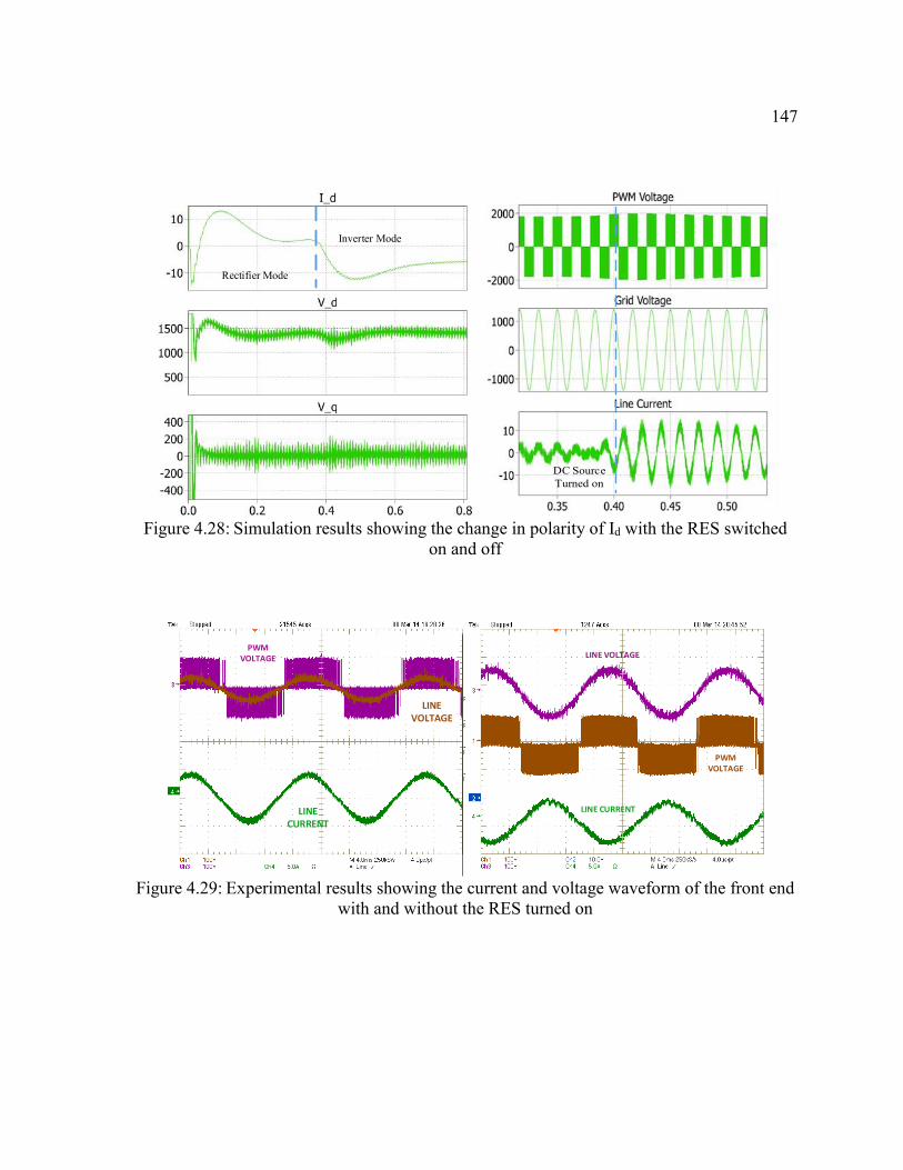
147
Rectifier Mode
Inverter Mode
DC Source
Turned on
Figure 4.28: Simulation results showing the change in polarity of Id with the RES switched
on and off
Figure 4.29: Experimental results showing the current and voltage waveform of the front end
with and without the RES turned on
LINE CURRENT
PWM VOLTAGE
LINE VOLTAGE
LINE CURRENT
LINE VOLTAGE
PWM VOLTAGE

148
4.13. UPS operation of a single phase SST
This section discusses the UPS operation of SST in case of grid failure.
RENEWABLE
SOURCE/
STORAGE
DC
LOCAL
LOAD
AC
BRIDGE 1
BRIDGE 2 BRIDGE 3
PCC
CRITICAL
LOAD
INPUT DC BUS
Figure 4.30: The single phase SST as a UPS system with a critical load
Fig. 4.30 shows the system setup for the UPS operation of the SST. The PCC of the SST with
the AC bus has a local AC load. The grid is interfaced with an AC solid state breaker that
islands the system in case of failure. The developed lab prototype doesn’t include the islanding
algorithm. Instead the system is islanded manually and the DSP unit is made aware. Under
islanded operation several mode changes take place in the controller both for the front and the
DC to DC stage. For the DC stage in grid connect mode the input current to bridge 2 drove the
phase shift angle between bridge 2 and bridge 1&3. However under islanded mode the RES

149
needs to regulate the input DC bus (Fig. 4.30) giving up MPPT mode of operation. The local
load will still be supplied. The front end will change into inverter mode of operation and will
regulate the PCC AC voltage. For the DC to DC stage, regulating the input DC bus is the most
critical function. And hence at the onset of islanding when the system goes through the black
start mode, the DC stage is commanded to shed its local load and regulate the input DC bus
voltage. After the PCC voltage has been established by the front end, the local load is supplied
by the DC stage and the local load bus ramps up. Fig. 4.31 shows the black start operation in
a flow chart form. Fig. 4.32 shows the experimental results with the islanding of the SST with
the load shedding functionality. The load shedding provides a ramp increase in the local load
while the AC bus power supply remains un-interrupted.
Islanding
Initiated
DC Stage sheds
local load
DC Stage
regulates the
input DC bus
Front end
changes to
inverter mode,
regulates PCC
AC voltage
DC Stage
regulates ramps
up the local load
Figure 4.31: Flow chart diagram of the black start system for the SST supplying a critical
load
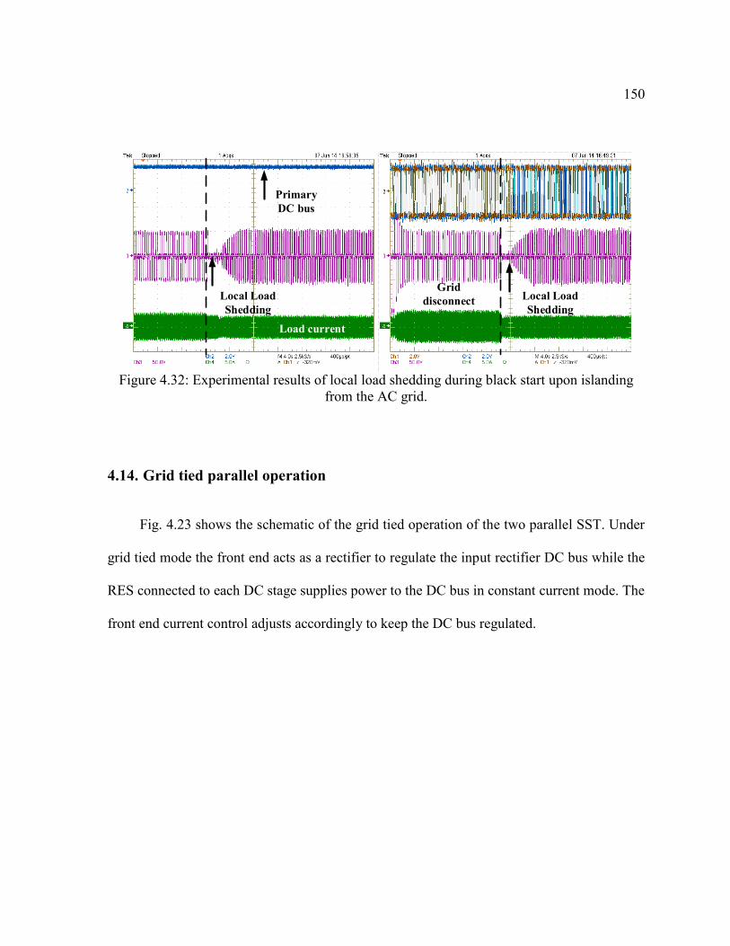
150
Local Load
Shedding
Primary
DC bus
Load current
Grid
disconnectLocal Load
Shedding
Figure 4.32: Experimental results of local load shedding during black start upon islanding
from the AC grid.
4.14. Grid tied parallel operation
Fig. 4.23 shows the schematic of the grid tied operation of the two parallel SST. Under
grid tied mode the front end acts as a rectifier to regulate the input rectifier DC bus while the
RES connected to each DC stage supplies power to the DC bus in constant current mode. The
front end current control adjusts accordingly to keep the DC bus regulated.
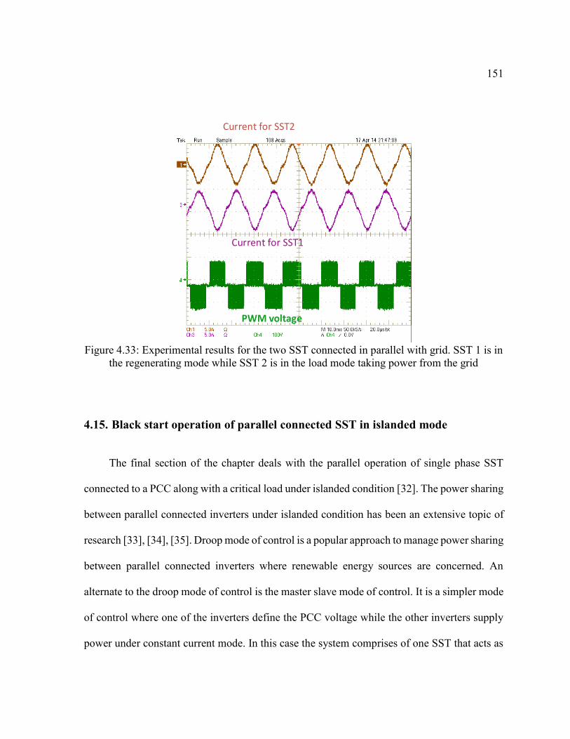
151
Current for SST1
Current for SST2
PWM voltage
Figure 4.33: Experimental results for the two SST connected in parallel with grid. SST 1 is in
the regenerating mode while SST 2 is in the load mode taking power from the grid
4.15. Black start operation of parallel connected SST in islanded mode
The final section of the chapter deals with the parallel operation of single phase SST
connected to a PCC along with a critical load under islanded condition [32]. The power sharing
between parallel connected inverters under islanded condition has been an extensive topic of
research [33], [34], [35]. Droop mode of control is a popular approach to manage power sharing
between parallel connected inverters where renewable energy sources are concerned. An
alternate to the droop mode of control is the master slave mode of control. It is a simpler mode
of control where one of the inverters define the PCC voltage while the other inverters supply
power under constant current mode. In this case the system comprises of one SST that acts as

152
a master and defines the PCC voltage. The front end of the master SST acts as an inverter that
controls the voltage of the PCC bus while the slave SST front end has two options.
1) The slave front end acts as a rectifier while the DC stage connected to the DC bus pushes
power. Power flow in the DC stage is controlled by MPPT driven input current control.
This has the advantage of proper utilization of the RES connected to the slave SST.
2) The second option is that the front end of the slave SST acts as a current controlled inverter
and pushes power in to the PCC. In this case the DC stage of the slave SST controls the
input DC bus voltage of the front end.
Islanding
Initiated
Master
SST
DC to DC stage
starts to regulate
the Input DC bus
Front end
switches to
inverter mode
Slave
SST
DC to DC stage
continues to
work with input
current control
Front end
continue to
work as rectifier
Figure 4.34: Flow chart diagram for the black start operation with the slave SST front end
acting as a rectifier under islanded mode
Fig. 4.34 shows the black start up control flow chart diagram as per mode 1 discussed above.
As soon as islanding has been detected and the grid breaker has been tripped, the master front

153
end reverts to inverter mode while simultaneously the DC to DC stage controls the input DC
bus voltage. However there is no change in the control for the slave SST. Its front end continue
to work as rectifier and the DC stage inject power in the input DC bus.
Input DC bus (SST1)
Input DC bus (SST2)
Grid Status
Load voltage
Grid Status
Load voltage
SST 1 current
SST 2 current
Figure 4.35: Experimental result of the black start of the parallel SST system with the slave
SST front end working as a rectifier.
Fig. 4.35 shows the experimental result for the black start for the parallel SST system. It is
seen that the load voltage sags at the time of grid failure. The black start introduces an
undesirable transient on the load. In order to improve the load transient during the black start
operation, the slave SST mode change is considered. In the grid connected mode front end of
the slave SST works as a rectifier. However on grid disconnect the slave SST changes to
current control inverter. Its DC to DC stage controls the inverter DC bus. On the master SST,
the mode change remains same on the front end however the DC stage goes through load
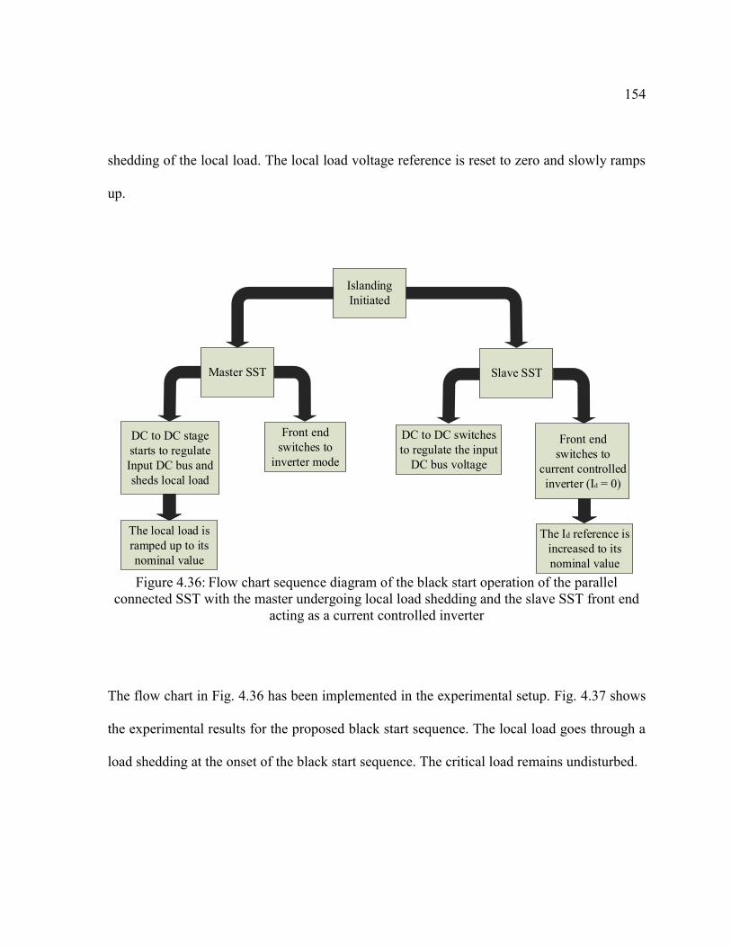
154
shedding of the local load. The local load voltage reference is reset to zero and slowly ramps
up.
Islanding
Initiated
Master SST
DC to DC stage
starts to regulate
Input DC bus and
sheds local load
Front end
switches to
inverter mode
Slave SST
DC to DC switches
to regulate the input
DC bus voltage
Front end
switches to
current controlled
inverter (Id = 0)
The local load is
ramped up to its
nominal value
The Id reference is
increased to its
nominal value Figure 4.36: Flow chart sequence diagram of the black start operation of the parallel
connected SST with the master undergoing local load shedding and the slave SST front end
acting as a current controlled inverter
The flow chart in Fig. 4.36 has been implemented in the experimental setup. Fig. 4.37 shows
the experimental results for the proposed black start sequence. The local load goes through a
load shedding at the onset of the black start sequence. The critical load remains undisturbed.

155
Load Voltage
Master SST current
Master SST local load
Slave SST local load
Grid disconnect
Figure 4.37: Experimental results of the black start operation under load shedding with the
critical load connected to SST 2 (slave DC stage)
Line Voltage
(PCC)
Line Current
(Master)
Figure 4.38: Black start without the feed-forward term on the master SST voltage controller

156
PCC voltage
Master Line
current
PCC voltage
Master Line
current
Figure 4.39: Experimental results of the black start operation showing the PCC voltage
regulated by the master
In order to have an uninterruptable voltage regulation on the PCC by the master, the reference
voltage is fed forward on the d-axes modulation index. Therefore the final modulation index
that goes to the PWM module for gate pulse generation is shown in (4.9).
𝑚𝑑𝑃𝑊𝑀 = 𝑚𝑑
𝑟𝑒𝑓(𝑓𝑒𝑒𝑑𝑓𝑜𝑟𝑤𝑎𝑟𝑑)+𝑚𝑑
𝑃𝐼 (4.9)
Here 𝑚𝑑𝑟𝑒𝑓(𝑓𝑒𝑒𝑑𝑓𝑜𝑟𝑤𝑎𝑟𝑑)
is 0.75 p.u. and 𝑚𝑑𝑃𝐼 is the output from the PI compensator. Without
the feed-forward the PCC voltage will go through a transient at the time of grid disconnect.
Fig. 4.38 and Fig. 4.39 shows the PCC bus voltage without and with the feed forward during
the black start. The feed forward loop takes care of the transient and makes the regulation
better.

157
4.16. Critical load placement in SST topology:
Critical load connected to the SST be it in the DC stage or the AC stage needs
uninterrupted power supply. Incase islanding has been detected and the grid shuts down it is
important to have the critical loads connected at certain points so that the SST can supply
uninterrupted power. In Fig. 4.40, the critical load points are marked in red. When the grid fails
it is the job of the master to regulate the PCC voltage so that there is minimum interruption.
The DC load connected to the master is assumed to be not critical. Hence a ramped reference
is given similar to Fig. 4.32. For the slave SST the critical load is connected to the DC stage
which can be considered as the norm. Thus the job of the slave SST is to regulate the local load
with minimum interruption while the excess power can be injected to the grid. However there
is a problem with this configuration for the load. Since the load is connected to the peripheral
limb as per Fig. 4.40, the power transfer takes place through duty cycle modulation as
explained in sec. 3.7. The duty cycle modulation itself is dependent on the phase shift between
the peripheral limbs and the central limb which in this case is linked with the winding
connected to the grid. Hence unless the front end starts injecting current to the grid, the phase
shift between the peripheral limb and the central limb will not develop and this constrains the
power supply to the critical load connected to the DC side. To remedy this on way is to link
the peripheral limb to the grid connected front end and connect the critical load to the central
limb as shown in Fig. 4.41. The second method may be is to simply increase the capacitor
connected to the slave SST (in blue in Fig. 4.41) so that during the black start the capacitor
supplies the transient energy while the phase shift between the peripheral and the central limb

158
is established. Fig. 4.42 shows the generalized system diagram with one master SST module
(red) and multiple slave module with their own critical load connected to the DC stage. In grid
connected mode the master SST is irrelevant. The SST front end act as rectifier maintain the
input DC bus. Both the front end and the renewable energy together supply the power to the
load connected to the central limb by phase shift mode of control.
RENEWABLE
SOURCE/
STORAGE
AC TO DC (SINGLE
PHASE)
DC LOAD MULTITERMINAL
HF ISOLATION
INPUT
FILTER
INDUCTOR
AC
AC LOAD
RENEWABLE
SOURCE/
STORAGE
AC TO DC (SINGLE
PHASE)
DC LOAD MULTITERMINAL
HF ISOLATION
INPUT
FILTER
INDUCTOR
MASTER SST
SLAVE SST
Figure 4.40: System diagram showing the critical load points
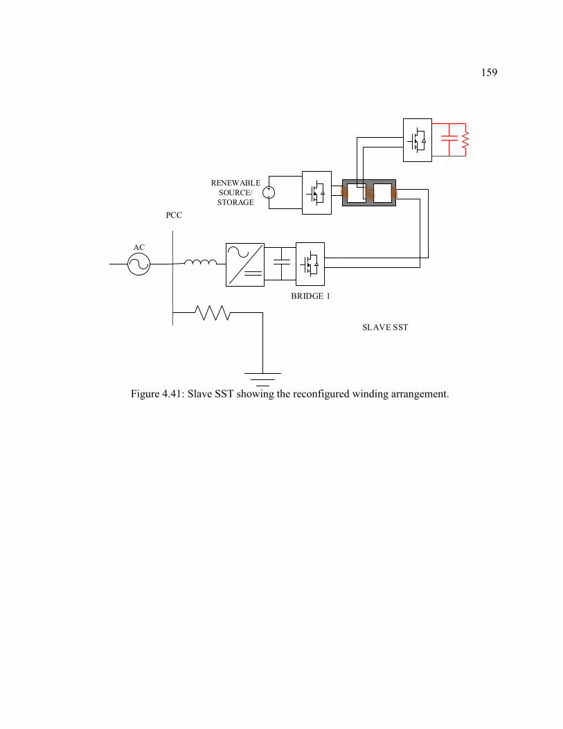
159
RENEWABLE
SOURCE/
STORAGE
AC
BRIDGE 1
PCC
SLAVE SST
Figure 4.41: Slave SST showing the reconfigured winding arrangement.

160
RENEWABLE
SOURCE/
STORAGE
AC
BRIDGE 1
PCC
RENEWABLE
SOURCE/
STORAGE
BRIDGE 1
MASTER DEFINES
VOLTAGE
SLAVEINPUT DC
BUS
INPUT DC
BUS
Figure 4.42: Slave SST showing the reconfigured winding arrangement.
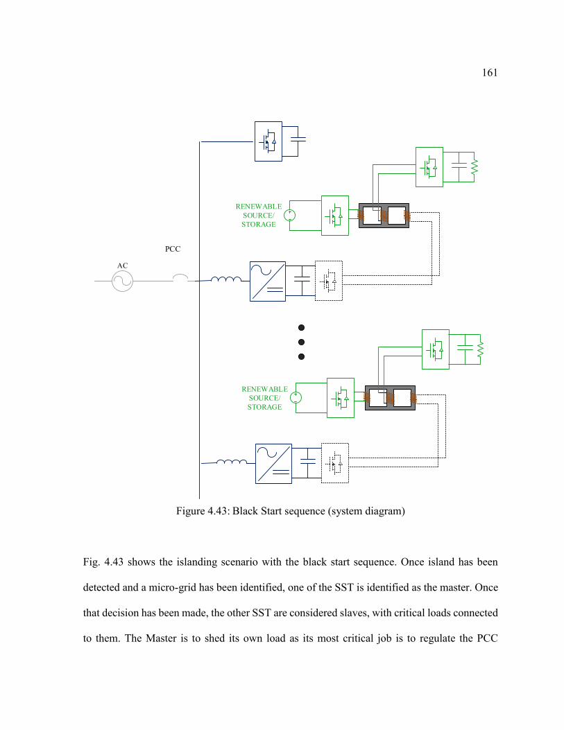
161
Figure 4.43: Black Start sequence (system diagram)
Fig. 4.43 shows the islanding scenario with the black start sequence. Once island has been
detected and a micro-grid has been identified, one of the SST is identified as the master. Once
that decision has been made, the other SST are considered slaves, with critical loads connected
to them. The Master is to shed its own load as its most critical job is to regulate the PCC
RENEWABLE
SOURCE/
STORAGE
AC
PCC
RENEWABLE
SOURCE/
STORAGE

162
voltage. Parallel to this the slave SST will maintain its critical load with the assumption that
the renewable energy source coupled with the load capacitor (marked in blue in Fig. 4.43)
provides enough energy to maintain uninterrupted power. Once the PCC voltage has been
established, the rectifier bus further supports the critical load. In case the renewable energy
sources have excess of energy, the front end converter provides a path for the power to flow
out. In that case the master has to provide for storage for the excess energy.
Master
SST
Regulate the
Input DC bus
& shed local
load
PCC Voltage
control inverter
mode
Slave
SST
RES provides
power to
local(critical) load
Front end
still acts as
rectifier
Local load is
ramped up
Islanding
Initiated
Master SST
identified
YES
O/P bridge
duty cycle
modulated
Power is
pushed out
NO
O/P bridge provides
power to critical load
Figure 4.44: black start sequence flow chart diagram

163
Grid Status
PCC
Voltage
Line
current
Figure 4.45: Black Start transient showing the PCC voltage and the line current
PCC Voltage
Line current
Grid
Status
Master
DC bus Grid Status
Slave local
load (critical)
PCC Voltage
(critical)
Line current
Figure 4.46: Experimental result showing the critical loads being kept undisturbed at the
point of black start
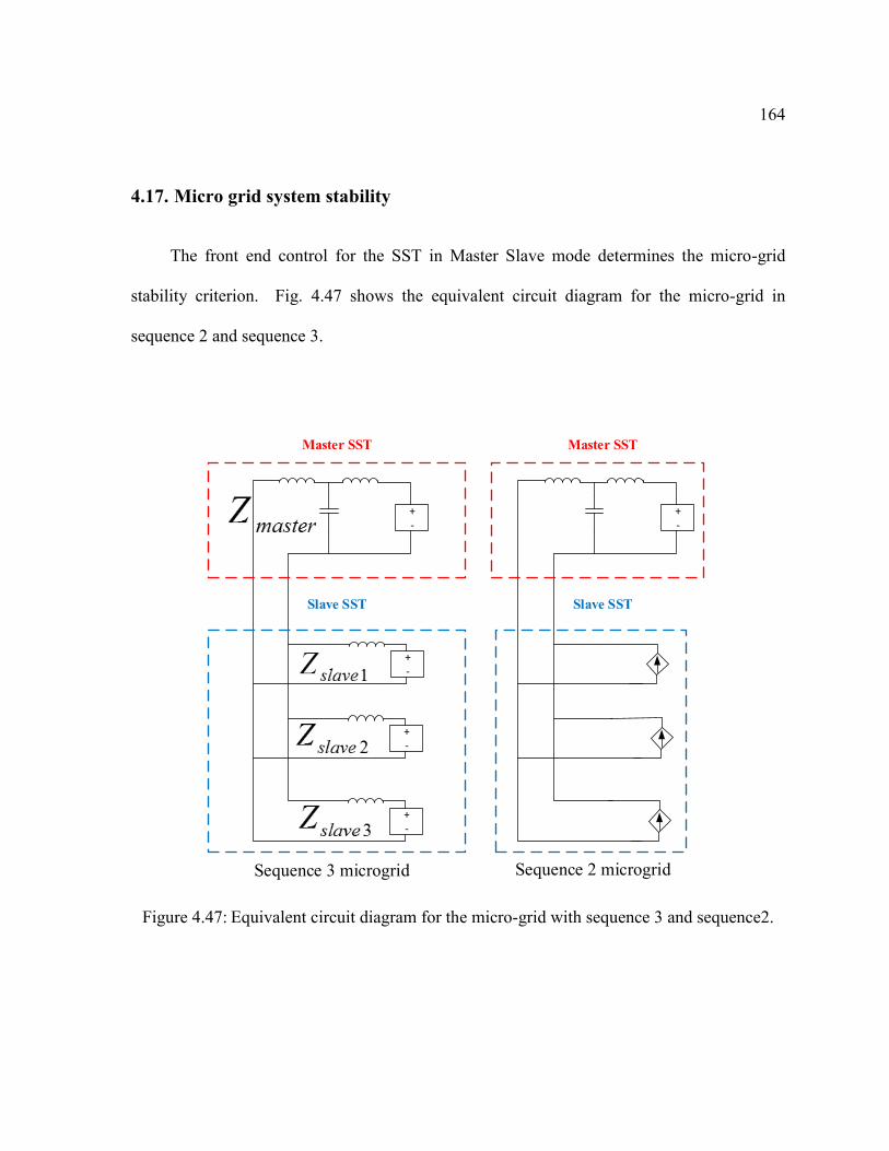
164
4.17. Micro grid system stability
The front end control for the SST in Master Slave mode determines the micro-grid
stability criterion. Fig. 4.47 shows the equivalent circuit diagram for the micro-grid in
sequence 2 and sequence 3.
+-
+-
+-
+-
Master SST
Slave SST
+-
Master SST
Slave SST
Sequence 3 microgrid Sequence 2 microgrid
Figure 4.47: Equivalent circuit diagram for the micro-grid with sequence 3 and sequence2.

165
From Fig. 4.47 the sequence 2 micro-grid is inherently stable since the voltage sources and
current sources do not interact with each other. However since in sequence 3 the front ends of
the SST are all voltage sources, interaction is possible if the close loop controllers are not
designed properly. The criterion for the closed loop stability is
𝑍𝑚𝑎𝑠𝑡𝑒𝑟 ≪ 𝑍𝑠𝑙𝑎𝑣𝑒1||𝑍𝑠𝑙𝑎𝑣𝑒2||𝑍𝑠𝑙𝑎𝑣𝑒3 ∀ 𝑓 < 𝑓𝑠𝑤𝑖𝑡𝑐ℎ𝑖𝑛𝑔 (4.10)
Therefore the close loop impedance of the master SST has to be lesser than the parallel
combination of the impedances of all the slave SST [36]. With the increase in the number of
slave SST this criterion gets more and more difficult to satisfy. Hence the sequence 2 is the
best suited from the stability point of view. This leads to the sequence 4 explained in the
following section.
4.18. Black Start Sequence 4
The sequence 4 was adopted to obtain greater stability for the micro-grid under transients.
Fig. 4.48 shows the flow chart control diagram for the sequence 4. Here the front end acts like
an inverter as in sequence 2 but the critical load is connected to the central limb and remains
uninterrupted during the black start sequence. The tertiary limb is connected to the front end
bridge and voltage of the DC bus is controlled. Upon islanding the following sequence of
events take place:
• Master SST regulates PCC bus (same in all the sequences)
• Front end is current controlled inverter
• Bridge 1 & 2 are in phase and Bridge 3 is lagging both 1 & 2 (Fig. 4.48).

166
• Phase shift between bridge 1 or 2 and 3 is determined by the voltage regulation at the
input bus of bridge 1
• Load can be regulated by PWM modulating Bridge 3
Figure 4.48: Sequence 4 Black start circuit diagram
RES
BRIDGE 1
PCC
BRIDGE 2
BRIDGE 3
In-phase
LaggingMASTER SST
SLAVE SST
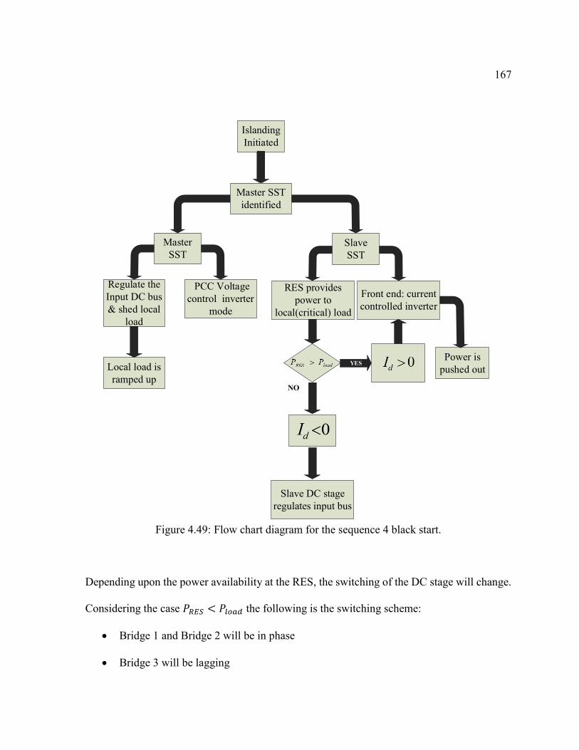
167
Figure 4.49: Flow chart diagram for the sequence 4 black start.
Depending upon the power availability at the RES, the switching of the DC stage will change.
Considering the case 𝑃𝑅𝐸𝑆 < 𝑃𝑙𝑜𝑎𝑑 the following is the switching scheme:
Bridge 1 and Bridge 2 will be in phase
Bridge 3 will be lagging
Master
SST
Regulate the
Input DC bus
& shed local
load
PCC Voltage
control inverter
mode
Slave
SST
RES provides
power to
local(critical) load
Front end: current
controlled inverter
Local load is
ramped up
Islanding
Initiated
Master SST
identified
YESPower is
pushed out
NO
Slave DC stage
regulates input bus

168
The phase shift between 1or 2 and bridge 3 is dependent on the bridge 1 DC bus voltage.
Voltage regulation on the load bridge 3 is made by duty cycle modulating bridge 3
The 𝐼𝑟𝑒𝑓𝑑 is negative (i.e. power is flowing from the PCC into the DC stage) and a
function of the difference between the power available at RES and the power demand
at the load.
Figure 4.50: Experimental results for the black start sequence 4
Fig. 4.50 shows the experimental results at the instant of black start. The DC bus at the SST2
local load is undisturbed and the DC bus at the input of the master SST front end SST is
undisturbed as well. However the SST2 DC bus after its front end has a sag that proves that
the 𝐼𝑟𝑒𝑓𝑑 given to the front end converter is not high enough to push the input voltage of the
SST2 front end high enough to its rated value. This shows that this mode of control needs a
very good supervisory control for the power matching. The second figure shows the current
Line Current
SST2 load
SST1 DC bus
SST2 DC bus
SST1 line
current
SST2 line
current
SST2 PWM
voltage

169
pushed out by the two SST (master and slave). They are in opposite polarity showing the
𝐼𝑚𝑎𝑠𝑡𝑒𝑟𝑑 > 0 while 𝐼𝑚𝑎𝑠𝑡𝑒𝑟
𝑑 < 0 as it should be as per the control.
Figure 4.51: PCC voltage at the instant of black start (sequence 4)
Fig. 4.51 shows the PCC voltage at the instant of black start. Although there is a sag for a few
cycles the voltage comes up and the micro-grid is stable. In the case where 𝑃𝑅𝐸𝑆 > 𝑃𝑙𝑜𝑎𝑑, the
following is the switching scheme:
Bridge 1 and Bridge 3 are lagging, Bridge 2 is the leading bridge.
The phase shift angle is determined by the load requirement at Bridge 3.
The bridge 1 DC bus is maintained by PWM modulating bridge 1
SST1
line
current
PCC
Voltage
SST1
DC bus
Grid

170
The 𝐼𝑟𝑒𝑓𝑑 is positive (i.e. power is flowing to the PCC from the DC stage) and is a
function of 𝑃𝑅𝐸𝑆 − 𝑃𝑙𝑜𝑎𝑑. This mode is very similar to the sequence 2.
Figure 4.52: DC stage and front end current wave form after islanding has occurred
Fig. 4.52 shows the steady state results for the islanded conditions with the DC stage showing
the PWM voltage waveforms and the AC stage showing the current injected into the load. So
long in the discussions the condition that 𝑃𝑅𝐸𝑆 >> 𝑃𝑙𝑜𝑎𝑑, has been neglected. But this is a
possibility when the generated RES power is higher than any load requirement in the micro-
grid. In that case the master needs to supply storage to store the excess power. Fig. 4.54 shows
the simulation results when the 𝐼𝑟𝑒𝑓𝑑 for the front end is ramped up from 5A to 10 A. The phase
shift angle for the master is revered and the power flows into the DC stage and provided that
there is a storage available, power flows into the storage device. The power flow diagram is
shown in Fig. 4.53.
SST2
Front end
current
SST2
Bridge
voltages
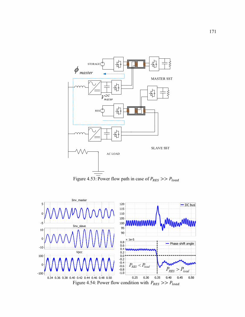
171
Figure 4.53: Power flow path in case of 𝑃𝑅𝐸𝑆 >> 𝑃𝑙𝑜𝑎𝑑
Figure 4.54: Power flow condition with 𝑃𝑅𝐸𝑆 >> 𝑃𝑙𝑜𝑎𝑑
STORAGE
AC LOAD
RES
MASTER SST
SLAVE SST

172
4.19. Conclusions
In this chapter the solid state transformer application for the DAB converter was
discussed. The results obtained in this chapter are summarized as follows:
In the single phase cascaded solid state transformer topology a DC-DC stage was
proposed based on the MLC-DAB topology. The proposed topology was shown to
require no voltage balance for the cascaded stages and the DC stage. Experimental
prototype of the MLC integrated SST was developed and the voltage balance was
shown under startup and voltage sag conditions.
During hard start to a single phase grid, the in rush current problem was shown for
the MLC-SST as well as the conventional SST topology. To limit the inrush current
a soft start algorithm was developed and implemented in a single phase cascaded
SST topology. The algorithm was verified with an experimental prototype using a
DC power supply for starting the SST, and the line current was shown to be limited
during startup.
For integrating renewable energy sources to the grid, a Renewable Energy Hub
topology was proposed based on the MLC-DAB topology with one of the
peripheral limbs grid tied.
A parallel SST based micro-grid test bed was developed in hardware consisting of
two MLC-SST connected in parallel. The MLC-SST have renewable energy
sources connected to the DC terminal. Steady state grid tied operation was shown
with the sources operating in input current control mode.

173
A black start sequence was developed for a single SST supplying a critical load
connected to the AC bus with load shedding on the local load connected to the SST.
A black start sequence was developed for two SST supplying a critical load, where
power balance between the SST are obtained using master-slave mode of control.
Based on the critical loads connected to the SST, a black start sequences were
developed and experimentally verified such that uninterrupted power is supplied to
the critical loads.

174
Conclusion
In the present thesis, novel current control strategies were developed for the Dual Active
Bridge DC to DC converter. A multi-terminal Dual Active Bridge converter was developed for
the purpose of integration of multiple renewable energy sources. A solid state transformer
application for the dual active bridge converter was developed to demonstrate grid integration
of renewable energy sources.
5.1. Summary of the main results
The main results obtained in the present thesis are summarized as follows:
A duty cycle mode of control was developed for the dual active bridge
converter. The proposed control was shown to remove DC bias from the high
frequency isolation transformer current.
A novel digital predictive current mode control was developed for the dual
active bridge converter. The predictive control can be classified as follows:
1. Phase shift control, where the transformer current is sampled once in the
switching cycle and the output of the controller is the phase shift angle.
2. Duty cycle control, where the transformer current is sampled twice in the
switching cycle and the output of the controller is the duty cycle that
modulates the secondary bridges of the DAB converter.

175
Sensitivity analysis of the predictive controller was done with respect to the
leakage inductance of the transformer. A compensation algorithm was
developed to make the controller insensitive with the variation in the leakage
inductance. The algorithm was experimentally verified in a hardware test bed
where an error in the leakage inductance was intentionally provided to the
controller.
The predictive phase shift control and the predictive duty cycle control were
both experimentally verified with a step change in the current reference and it
was shown that the controller is capable to track the change with in one cycle.
In the dual active bridge high frequency transformer, a moving window
averaging was done to track the DC bias in the magnetizing current. A
compensation algorithm was implemented by giving a compensating bias in the
switches (primary or secondary) and the DC bias compensation was
demonstrated.
For the purpose of integrating multiple renewable energy sources a multi-input
single output multi terminal dual active bridge converter was developed using
a multi-limb core transformer for the high frequency isolation stage. Electrical
equivalent circuit for the transformer was developed using the gyrator concept.
The power transfer equation was developed and the small signal characteristics
were analyzed.

176
Analysis was done to show the multi-limb transformer based DAB topology
using less copper and magnetic core material compared to a series connected
multi-terminal DAB.
A PWM based input current control was developed to integrate different
renewable sources operating at different power points. The developed control
algorithm was experimentally verified in a lab test bed where the multi-limb-
core based dual active bridge converter was developed with four input terminals
and one output terminal.
For the multi-terminal dual active bridge converter, a power smoothing
algorithm was developed where one of the input terminals were connected to
an oscillating power source (wave energy emulator) and another input terminal
to a storage device (battery). The developed algorithm was experimentally
demonstrated to provide a regulated output using the battery as an energy buffer
by alternatingly charging and discharging it.
Solid state transformer application of the multi-terminal dual active bridge
converter was demonstrated for the purpose of grid integration of renewable
energy sources. Analysis was done followed by experimental verification to
show the multi-terminal topology having a simpler control in terms of voltage
balance, compared to a two terminal DAB topology.
A soft start algorithm was developed for starting then solid state transformer
using an auxiliary power supply and integrating it with the grid. The algorithm

177
was experimentally verified in a test bed and was shown to reduce inrush
currents at startup.
A micro-grid test bed was developed with two single phase solid state
transformer with the multi-terminal dual active bridge converter for the DC
stage. Islanding was done and a black start sequence was developed.
The critical load points in the micro-grid was recognized and black start
sequences were developed to supply uninterrupted power to the critical loads.
The different black start sequences were experimentally verified and the un-
interruption at critical load points were demonstrated during the instant of
islanding.
5.2. Further scope of future research:
Since the control algorithms and topology developed in the thesis has been demonstrated
on a low voltage prototype, high voltage application can be developed in the future.
The predictive current control algorithm from chapter 2 was focused on a single phase
DAB topology, a similar predictive current mode controller may be developed for the three
phase DAB topology. The DC bias monitoring algorithm as developed for a single phase DAB
transformer may be implemented for a three phase transformer for the three phase DAB
topology. A different reference can be adopted for the three phase topology. Instead of
implementing the controller in the time domain as has been implemented in chapter 2, a space
vector based approach can be adopted for implementing the control in three phase domain.

178
The multi-limb core transformer based DAB developed in chapter 3 may be implemented
at higher voltage. Due to high 𝑑𝑣 𝑑𝑡⁄ at higher voltage, common mode currents will be an
important constraints in the design of the transformer.
The micro-grid application for the MLC-DAB based SST was developed for a low
voltage prototype in chapter 4. A high voltage prototype may be built with more renewable
energy integration and storage integration. Islanding algorithm may be implemented with grid
voltage sag and swell detection. Under islanded condition the stability of the micro-grid may
be studied with power fluctuation in the renewable energy sources. Appropriate sizing of the
storage components can be done based on these power fluctuations in the renewable energy
sources.

179
REFERENCES
[1] Tiefu Zhao, “Design and Control of a Cascaded H-Bridge Converter based Solid
State Transformer (SST)” , Thesis for the degree for Doctor of Philosophy, 2010.
[2] Xu She, “Control and Design of a High Voltage Solid State Transformer and its
Integration with Renewable Energy Resources and Microgrid System”, Thesis
for the degree for Doctor of Philosophy, 2013.
[3] Du, Yu; Huang, Alex Q.; Yu, Xunwei; Li, Jun, "Droop controller design methods
for isolated DC-DC converter in DC grid battery energy storage applications,"
Applied Power Electronics Conference and Exposition (APEC), 2013 Twenty-
Eighth Annual IEEE , vol., no., pp.1630,1637, 17-21 March 2013
[4] Falcones, S.; Ayyanar, R.; Xiaolin Mao, "A DC–DC Multiport-Converter-Based
Solid-State Transformer Integrating Distributed Generation and Storage," Power
Electronics, IEEE Transactions on , vol.28, no.5, pp.2192,2203, May 2013
[5] Zhenhua Jiang; Xunwei Yu, "Hybrid DC- and AC-Linked Microgrids: Towards
Integration of Distributed Energy Resources," Energy 2030 Conference, 2008.
ENERGY 2008. IEEE , vol., no., pp.1,8, 17-18 Nov. 2008
[6] Mustansir H. Kheraluwala ,“High power high frequency DC to DC converters”,
Thesis for the degree for Doctor of Philosophy, 1991.
[7] R.W. DeDoncker, D.M. Divan, M.H. Kheraluwala “A three phase Soft-Switched
High Power Density DC-DC converter”. IEEE transactions on industry
applications, vol. 27, no. 1, Jan/Feb,1991
[8] Krismer, F.; Kolar, J.W., "Accurate small-signal model for an automotive
bidirectional Dual Active Bridge converter," Control and Modeling for Power
Electronics, 2008. COMPEL 2008. 11th Workshop on , vol., no., pp.1,10, 17-20
Aug. 2008.
[9] Georgios D. Demetriades, “On small-signal analysis and control of the single and
dual-active bridge topologies”, Thesis for the degree for Doctor of Philosophy,
2005

180
[10] Jingquan Chen; Prodic, A.; Erickson, R.W.; Maksimovic, D., "Predictive digital
current programmed control," Power Electronics, IEEE Transactions on , vol.18,
no.1, pp.411,419, Jan 2003
[11] Xunwei Yu; Xu She; Huang, A, "Hierarchical power management for DC
microgrid in islanding mode and Solid State transformer enabled mode,"
Industrial Electronics Society, IECON 2013 - 39th Annual Conference of the
IEEE , vol., no., pp.1656,1661, 10-13 Nov. 2013
[12] Barazarte, R.Y.; Gonzalez, G.G.; Ehsani, M., "Generalized Gyrator Theory,"
Power Electronics, IEEE Transactions on , vol.25, no.7, pp.1832,1837, July 2010
[13] Hongfei Wu; Peng Xu; Haibing Hu; Zihu Zhou; Yan Xing, "Multiport Converters
Based on Integration of Full-Bridge and Bidirectional DC–DC Topologies for
Renewable Generation Systems," Industrial Electronics, IEEE Transactions on ,
vol.61, no.2, pp.856,869, Feb. 2014
[14] Everts, J.; Van Den Keybus, J.; Driesen, J., "Switching control strategy to extend
the ZVS operating range of a Dual Active Bridge AC/DC converter," Energy
Conversion Congress and Exposition (ECCE), 2011 IEEE , vol., no.,
pp.4107,4114, 17-22 Sept. 2011
[15] Jun Huang; Yue Wang; Yuan Gao; Wanjun Lei; Ning Li, "Modified unified
PWM control to operate the dual active bridge converters under ZVS in the whole
load range," ECCE Asia Downunder (ECCE Asia), 2013 IEEE , vol., no.,
pp.620,625, 3-6 June 2013
[16] Erickson & Maksimovic “Fundamentals of Power Electronics”, Second Edition,
Springer Internatonal Edition, 2005.
[17] Inoue, S.; Akagi, H., "A Bidirectional DC–DC Converter for an Energy Storage
System With Galvanic Isolation," Power Electronics, IEEE Transactions on ,
vol.22, no.6, pp.2299,2306, Nov. 2007
[18] Seunghun Baek, “Design considerations of High Voltage and High Frequency
Transformers for Solid State Transformer Applications” Thesis for the degree for
Masters of Science, 2009
[19] Seunghun Baek; Dutta, S.; Bhattacharya, S., "Characterization of a three-phase
dual active bridge DC/DC converter in wye-delta connection for a high frequency

181
and high power applications," Energy Conversion Congress and Exposition
(ECCE), 2011 IEEE , vol., no., pp.4183,4188, 17-22 Sept. 2011
[20] Seunghun Baek; Bhattacharya, S., "Analytical modeling of a medium-voltage
and high-frequency resonant coaxial-type power transformer for a solid state
transformer application," Energy Conversion Congress and Exposition (ECCE),
2011 IEEE , vol., no., pp.1873,1880, 17-22 Sept. 2011
[21] Xu She; Burgos, R.; Gangyao Wang; Fei Wang; Huang, A.Q., "Review of solid
state transformer in the distribution system: From components to field
application," Energy Conversion Congress and Exposition (ECCE), 2012 IEEE ,
vol., no., pp.4077,4084, 15-20 Sept. 2012
[22] Dutta, S.; Roy, S.; Bhattacharya, S., "A multi-terminal DC to DC converter
topology with power accumulation from renewable energy sources with
unregulated DC voltages," Applied Power Electronics Conference and
Exposition (APEC), 2013 Twenty-Eighth Annual IEEE , vol., no., pp.1124,1130,
17-21 March 2013
[23] Roy, S.; Umanand, L., "Integrated Magnetics-Based Multisource Quality AC
Power Supply," Industrial Electronics, IEEE Transactions on , vol.58, no.4,
pp.1350,1358, April 2011
[24] Markakis, A; Holderbaum, W.; Potter, B., "A comparison between bond graphs
switching modelling techniques implemented on a boost dc-dc converter,"
Telecommunications Energy Conference (INTELEC), 2011 IEEE 33rd
International , vol., no., pp.1,7, 9-13 Oct. 2011
[25] Umesh Rai, B.; Umanand, L., "Bond graph toolbox for handling complex
variable," Control Theory & Applications, IET , vol.3, no.5, pp.551,560, May
2009
[26] Muhlethaler, J.; Biela, J.; Kolar, J.W.; Ecklebe, A, "Improved core loss
calculation for magnetic components employed in power electronic system,"
Applied Power Electronics Conference and Exposition (APEC), 2011 Twenty-
Sixth Annual IEEE , vol., no., pp.1729,1736, 6-11 March 2011
[27] Muhlethaler, J.; Biela, J.; Kolar, J.W.; Ecklebe, A, "Core losses under DC bias
condition based on Steinmetz parameters," Power Electronics Conference
(IPEC), 2010 International , vol., no., pp.2430,2437, 21-24 June 2010
182
[28] Madhusoodhanan, S.; Tripathi, A; Kadavelugu, A; Hazra, S.; Patel, D.; Mainali,
K.; Bhattacharya, S.; Hatua, K., "Experimental validation of the steady state and
transient behavior of a transformerless intelligent power substation," Applied
Power Electronics Conference and Exposition (APEC), 2014 Twenty-Ninth
Annual IEEE , vol., no., pp.3477,3484, 16-20 March 2014
[29] Madhusoodhanan, S.; Bhattacharya, S.; Hatua, K., "A unified control scheme for
harmonic elimination in the front end converter of a 13.8 kV, 100 kVA
transformerless intelligent power substation grid tied with LCL filter," Applied
Power Electronics Conference and Exposition (APEC), 2014 Twenty-Ninth
Annual IEEE , vol., no., pp.964,971, 16-20 March 2014
[30] Madhusoodhanan, S.; Bhattacharya, S.; Hatua, K., "Control technique for 15 kV
SiC IGBT based active front end converter of a 13.8 kV grid tied 100 kVA
transformerless intelligent power substation," Energy Conversion Congress and
Exposition (ECCE), 2013 IEEE , vol., no., pp.4697,4704, 15-19 Sept. 2013
[31] Tiefu Zhao; Gangyao Wang; Jie Zeng; Dutta, S.; Bhattacharya, S.; Huang, A.Q.,
"Voltage and power balance control for a cascaded multilevel solid state
transformer," Applied Power Electronics Conference and Exposition (APEC),
2010 Twenty-Fifth Annual IEEE , vol., no., pp.761,767, 21-25 Feb. 2010
[32] Parks, N.; Dutta, S.; Ramachandram, V.; Hatua, K.; Bhattacharya, S., "Black start
control of a solid state transformer for emergency power restoration," Energy
Conversion Congress and Exposition (ECCE), 2012 IEEE , vol., no., pp.188,195,
15-20 Sept. 2012
[33] Dasgupta, S.; Mohan, S.N.; Sahoo, S.K.; Panda, S.K., "A Plug and Play
Operational Approach for Implementation of an Autonomous-Micro-Grid
System," Industrial Informatics, IEEE Transactions on , vol.8, no.3, pp.615,629,
Aug. 2012
[34] Arulampalam, A; Mithulananthan, N.; Bansal, R.C.; Saha, T.K., "Micro-grid
control of PV-Wind-Diesel hybrid system with islanded and grid connected
operations," Sustainable Energy Technologies (ICSET), 2010 IEEE International
Conference on , vol., no., pp.1,5, 6-9 Dec. 2010
[35] Nagliero, A; Mastromauro, R.A; Monopoli, V.G.; Liserre, M.; Dell'Aquila, A,
"Analysis of a universal inverter working in grid-connected, stand-alone and
micro-grid," Industrial Electronics (ISIE), 2010 IEEE International Symposium
on , vol., no., pp.650,657, 4-7 July 2010

183
[36] Krishnamurthy, H.; Ayyanar, R., "Stability analysis of cascaded converters for
bidirectional power flow applications," Telecommunications Energy Conference,
2008. INTELEC 2008. IEEE 30th International , vol., no., pp.1,8, 14-18 Sept.
2008
[37] Chattopadhyay, S.; Das, S., "A Digital Current-Mode Control Technique for DC–
DC Converters," Power Electronics, IEEE Transactions on , vol.21, no.6,
pp.1718,1726, Nov. 2006
[38] Demetriades, G.D.; Nee, H.P., "Characterisation of the Soft-switched Single-
Active Bridge Topology Employing a Novel Control Scheme for High-power
DC-DC Applications," Power Electronics Specialists Conference, 2005. PESC
'05. IEEE 36th , vol., no., pp.1947,1951, 16-16 June 2005
[29] Demetriades, G.D.; Nee, H-P, "Dynamic modeling of the Dual-Active Bridge
topology for high-power applications," Power Electronics Specialists
Conference, 2008. PESC 2008. IEEE , vol., no., pp.457,464, 15-19 June 2008
[40] Tan, N.M.L.; Abe, T.; Akagi, H., "Design and Performance of a Bidirectional
Isolated DC–DC Converter for a Battery Energy Storage System," Power
Electronics, IEEE Transactions on , vol.27, no.3, pp.1237,1248, March 2012
[41] Dutta, S.; Bhattacharya, S., "Predictive current mode control of single phase dual
active bridge DC to DC converter," Energy Conversion Congress and Exposition
(ECCE), 2013 IEEE , vol., no., pp.5526,5533, 15-19 Sept. 2013
[42] Dutta, S.; Bhattacharya, S.; Chandorkar, M., "A novel predictive phase shift
controller for bidirectional isolated dc to dc converter for high power
applications," Energy Conversion Congress and Exposition (ECCE), 2012 IEEE ,
vol., no., pp.418,423, 15-20 Sept. 2012
[43] Tao, H.; Kotsopoulos, A.; Duarte, J.L.; Hendrix, M.A.M.; , "A Soft-Switched
Three-Port Bidirectional Converter for Fuel Cell and Supercapacitor
Applications," Power Electronics Specialists Conference, 2005. PESC '05. IEEE
36th , vol., no., pp.2487-2493, 16-16 June 2005
[44] Klontz, K.W.; Divan, D.M.; Novotny, D.W., "An actively cooled 120 kW coaxial
winding transformer for fast charging electric vehicles," Industry Applications,
IEEE Transactions on , vol.31, no.6, pp.1257,1263, Nov/Dec 1995
184
[45] Rauls, M.S.; Novotny, D.W.; Divan, D.M., "Design considerations for high-
frequency coaxial winding power transformers," Industry Applications, IEEE
Transactions on , vol.29, no.2, pp.375,381, Mar/Apr 1993
[46] Zhijun Qian; Abdel-Rahman, O.; Pepper, M.; Batarseh, I.; , "Analysis and design
for paralleled three-port DC/DC converters with democratic current sharing
control," Energy Conversion Congress and Exposition, 2009. ECCE 2009. IEEE
, vol., no., pp.1375-1382, 20-24 Sept. 2009
[47] Baek, S.S.; Cougo, B.; Bhattacharya, S.; Ortiz, G., "Accurate equivalent circuit
modeling of a medium-voltage and high-frequency coaxial winding DC-link
transformer for solid state transformer applications," Energy Conversion
Congress and Exposition (ECCE), 2012 IEEE , vol., no., pp.1439,1446, 15-20
Sept. 2012
[48] Jain, A.K.; Ayyanar, R., "PWM Control of Dual Active Bridge: Comprehensive
Analysis and Experimental Verification," IEEE Transactions on Power
Electronics , vol.26, no.4, pp.1215,1227, April 2011
[49] Ortiz, G.; Uemura, H.; Bortis, D.; Kolar, J.W.; Apeldoorn, O., "Modeling of Soft-
Switching Losses of IGBTs in High-Power High-Efficiency Dual-Active-Bridge
DC/DC Converters," Electron Devices, IEEE Transactions on , vol.60, no.2,
pp.587,597, Feb. 2013
[50] Hengsi Qin; Kimball, J.W., "Solid-State Transformer Architecture Using AC–
AC Dual-Active-Bridge Converter," Industrial Electronics, IEEE Transactions
on , vol.60, no.9, pp.3720,3730, Sept. 2013
[51] Hengsi Qin; Kimball, J.W., "Ac-ac dual active bridge converter for solid state
transformer," Energy Conversion Congress and Exposition, 2009. ECCE 2009.
IEEE , vol., no., pp.3039,3044, 20-24 Sept. 2009
[52] Tuan Ngo; Jehyuk Won; Kwanghee Nam, "A single-phase bidirectional dual
active half-bridge converter," Applied Power Electronics Conference and
Exposition (APEC), 2012 Twenty-Seventh Annual IEEE , vol., no., pp.1127,1133,
5-9 Feb. 2012
[53] Hua Bai; Mi, C., "Eliminate Reactive Power and Increase System Efficiency of
Isolated Bidirectional Dual-Active-Bridge DC–DC Converters Using Novel
Dual-Phase-Shift Control," Power Electronics, IEEE Transactions on , vol.23,
no.6, pp.2905,2914, Nov. 2008

185
[54] Hengsi Qin; Kimball, J.W., "Generalized Average Modeling of Dual Active
Bridge DC–DC Converter," Power Electronics, IEEE Transactions on , vol.27,
no.4, pp.2078,2084, April 2012
[55] Guidi, G.; Pavlovsky, M.; Kawamura, A; Imakubo, T.; Sasaki, Y., "Improvement
of light load efficiency of Dual Active Bridge DC-DC converter by using dual
leakage transformer and variable frequency," Energy Conversion Congress and
Exposition (ECCE), 2010 IEEE , vol., no., pp.830,837, 12-16 Sept. 2010
[56] Seltzer, D.; Bloomquist, D.; Zane, R.; Maksimovic, D., "Gain-scheduled control
of multi angle phase shift modulated dual active bridge series resonant DC/DC
converters," Control and Modeling for Power Electronics (COMPEL), 2012
IEEE 13th Workshop on , vol., no., pp.1,7, 10-13 June 2012
[57] Filba-Martinez, A; Busquets-Monge, S.; Bordonau, J., "Modulation and
capacitor voltage balancing control of a three-level NPC dual-active-bridge DC-
DC converter," Industrial Electronics Society, IECON 2013 - 39th Annual
Conference of the IEEE , vol., no., pp.6251,6256, 10-13 Nov. 2013
[58] Tianyang Jiang; Xiliang Chen; Junming Zhang; Yousheng Wang, "New methods
to reduce circulating energy in dual active bridge converter," Applied Power
Electronics Conference and Exposition (APEC), 2013 Twenty-Eighth Annual
IEEE , vol., no., pp.2151,2155, 17-21 March 2013
[59] Hengsi Qin; Kimball, J.W., "Closed-loop control of DC-DC dual active bridge
converters driving single-phase inverters," Energy Conversion Congress and
Exposition (ECCE), 2012 IEEE , vol., no., pp.173,179, 15-20 Sept. 2012
[60] Ying Qiu; Liu, H.; Xiyou Chen, "Digital Average Current-Mode Control of
PWM DC–DC Converters Without Current Sensors," Industrial Electronics,
IEEE Transactions on , vol.57, no.5, pp.1670,1677, May 2010
[61] Xianjin Zhang; Caihong Fan, "Research on a novel DC-DC transformer,"
Electric Information and Control Engineering (ICEICE), 2011 International
Conference on , vol., no., pp.1619,1622, 15-17 April 2011