MODULAR FREQUENCY MULTIPLIER AND FILTERS FOR THE …
130
MODULAR FREQUENCY MULTIPLIER AND FILTERS FOR THE GLOBAL HAWK SNOW RADAR By Hara Madhav Talasila B. Tech., Acharya Nagarjuna University, 2014 Submitted to the graduate degree program in Electrical Engineering and Computer Science and the Graduate Faculty of the University of Kansas in partial fulfillment of the requirements for the degree of Master of Science. ________________________________ Chair: John D. Paden ________________________________ Co-Chair: Fernando Rodriguez-Morales ________________________________ Carlton Leuschen ________________________________ Christopher Allen Date Defended: 20 January, 2017
Transcript of MODULAR FREQUENCY MULTIPLIER AND FILTERS FOR THE …

MODULAR FREQUENCY MULTIPLIER AND FILTERS
FOR THE GLOBAL HAWK SNOW RADAR
By
Hara Madhav Talasila
B. Tech., Acharya Nagarjuna University, 2014
Submitted to the graduate degree program in Electrical Engineering and Computer Science
and the Graduate Faculty of the University of Kansas in partial fulfillment of the
requirements for the degree of Master of Science.
________________________________ Chair: John D. Paden
________________________________ Co-Chair: Fernando Rodriguez-Morales
________________________________ Carlton Leuschen
________________________________ Christopher Allen
Date Defended: 20 January, 2017

ii
The thesis committee for Hara Madhav Talasila
certifies that this is the approved version of the following thesis:
MODULAR FREQUENCY MULTIPLIER AND FILTERS
FOR THE GLOBAL HAWK SNOW RADAR
________________________________ John D. Paden
________________________________ Fernando Rodriguez-Morales
Date Approved: 31 January, 2017
iii
ABSTRACT
Remote sensing with radar systems on airborne platforms is key for wide-area data
collection to estimate the impact of ice and snow masses on rising sea levels. The NASA P-3B
and DC-8, as well as other platforms, successfully flew with multiple versions of the Snow
Radar developed at the Center for Remote Sensing of Ice Sheets. Compared to these manned
missions, the Global Hawk Uninhabited Aerial Vehicle can support flights with long endurance,
complex flight paths and flexible altitude operation up to 70,000 ft. This thesis documents the
process of adapting the 2-18 GHz Snow Radar to meet the requirements for operation on manned
and unmanned platforms from 700 ft to 70,000 ft. The primary focus of this work is the
development of an improved microwave chirp generator implemented with frequency
multipliers. The x16 frequency multiplier is composed of a series of x2 frequency multiplication
stages, overcoming some of the limitations encountered in previous designs. At each stage,
undesired harmonics are kept out of the passband and filtered. The miniaturized design presented
here reduces reflections in the chain, overall size, and weight as compared to the large and heavy
connectorized chain currently used in the Snow Radar. Each stage is implemented by a drop-in
type modular design operating at microwave and millimeter wavelengths; and realized with
commercial surface-mount integrated circuits, wire-bondable chips, and custom filters. DC
circuits for power regulation and sequencing are developed as well. Another focus of this thesis
is the development of the band-pass filters used in the frequency multiplier using different
distributed element filter technologies. Multiple edge-coupled band pass filters are fabricated on
alumina substrate based on the design and optimization in computer-aided design tools.
Interdigital cavity filter models developed in-house are validated through full-wave

iv
electromagnetic simulation and measurements. Overall, the measured results of the modular
frequency multiplier and filters match with the expected responses from original design and co-
simulation outputs. The design files, test setups, and simulation models are generalized to use
with new designs in the future.

v
ACKNOWLEDGEMENTS
I sincerely thank Dr. John D. Paden for his support throughout my Masters program. My
heart goes on to thank Dr. Fernando Rodriguez-Morales for kindly teaching me multiple skills to
accomplish this thesis. I deeply commend both my advisors for helping me to learn and their
guidance during failures. I am greatly indebted to Dr. Fernando and Dr. Paden for everything
they have done in my life. I also thank CReSIS, NASA and other organizations dedicated for
research funding many young researchers and students.
I am delighted to express my gratitude to Dr. Carl Leuschen and Dr. Christopher Allen
for enhancing my knowledge with important courses to implement the principles in design. I
thank Dr. S. Gogineni, Dr. S. Yan for developing the radar program and UWB instruments that
preceded this work. Dr. Jilu Li is likewise acknowledged for extending his support and expertise
to me. I extend my gratitude to Dr. Stiles, Dr. Demarest and Dr. Blunt for teaching the courses
useful for my applications. I feel honored to work and study with all these esteemed people at
CReSIS and KU.
I should also thank Dr. Torry Akins for his support with the Digital system. I sincerely
appreciate John Richardson from X-Microwave for his continuous support for the modular
multiplier. I thank Dr. Ralf Ihmels, Mician Inc, for providing the license for μWave Wizard. Ron
Miller from UltraSource has been a great support in fabrication of the small size high-frequency
Alumina filters.
I kindly thank Dr. Michael D. Glover (Late) of High Density Electronics Center,
University of Arkansas, for the help with wire-bonding Stage_0 boards. I am grateful to Dr. John

vi
Papapolymerou, Michigan State University, for providing the first results of the Alumina edge-
coupled filters. I am also grateful to Dr. Joseph Bardin, University of Massachusetts Amherst, for
providing the responses of mm-wave filters. I should also thank Dr. Nate Orloff and Dr. Dazhen
Gu from National Institute of Standards and Technology for providing the results for filters to
prove the repeatability of measurements.
I should thank Daniel Gomez-Garcia and Paulette Place for their help with information
about frequency multipliers and teaching me to build hardware. I should acknowledge the
amazing support of Aaron Paden for fabricating filters and bases required for my thesis. I thank
all my CReSIS colleagues and staff for giving me a good time at work. I also acknowledge the
design works of Jay Mc Daniel, Kah Ho Tee and others for their direct and indirect support for
the Global Hawk Snow Radar system. Finally, I extend my acknowledgements to all my well-
wishers and friends.
To conclude, I thank my parents Sri. Suresh and Smt. Lakshmi and my sister Deva Saroja
for motivating me to pursue Masters degree in USA. I would love to dedicate this work to
recently departed member of our family, Miss Lucy. I also thank all my family members for
extending their support to me.
ThanKU everyone !!!
vii
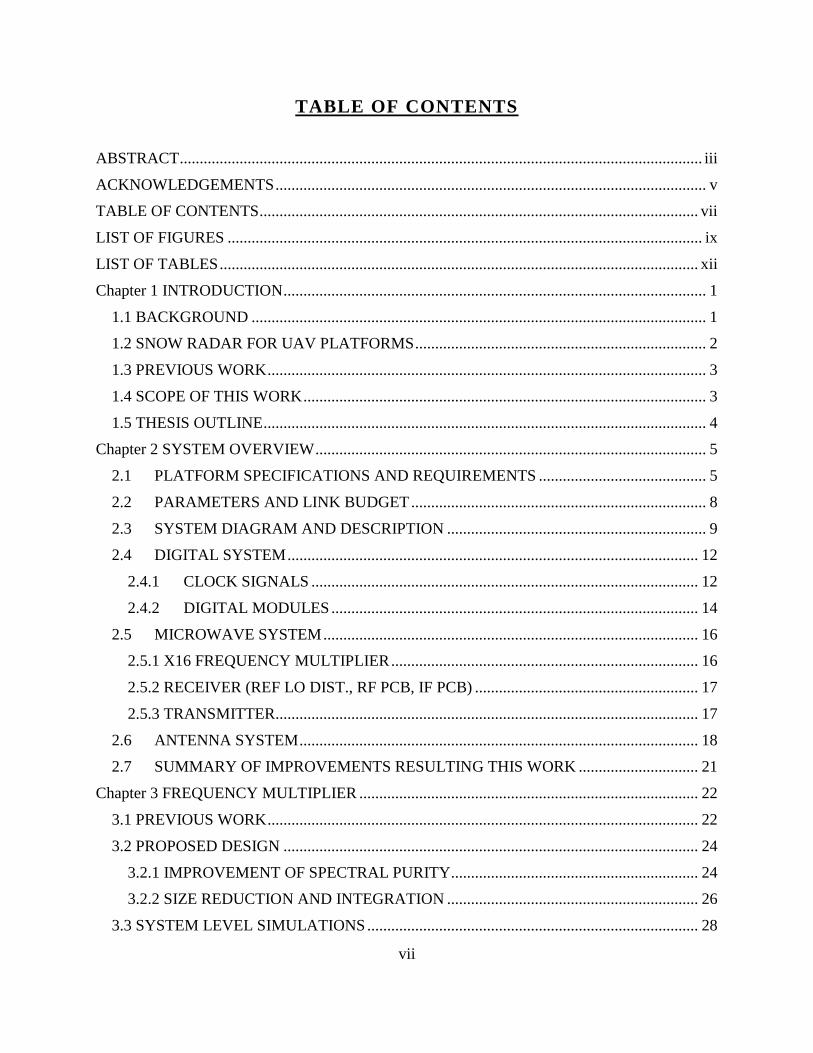
TABLE OF CONTENTS
ABSTRACT ................................................................................................................................... iii
ACKNOWLEDGEMENTS ............................................................................................................ v
TABLE OF CONTENTS .............................................................................................................. vii
LIST OF FIGURES ....................................................................................................................... ix
LIST OF TABLES ........................................................................................................................ xii
Chapter 1 INTRODUCTION .......................................................................................................... 1
1.1 BACKGROUND .................................................................................................................. 1
1.2 SNOW RADAR FOR UAV PLATFORMS ......................................................................... 2
1.3 PREVIOUS WORK .............................................................................................................. 3
1.4 SCOPE OF THIS WORK ..................................................................................................... 3
1.5 THESIS OUTLINE ............................................................................................................... 4
Chapter 2 SYSTEM OVERVIEW .................................................................................................. 5
2.1 PLATFORM SPECIFICATIONS AND REQUIREMENTS .......................................... 5
2.2 PARAMETERS AND LINK BUDGET .......................................................................... 8
2.3 SYSTEM DIAGRAM AND DESCRIPTION ................................................................. 9
2.4 DIGITAL SYSTEM ....................................................................................................... 12
2.4.1 CLOCK SIGNALS ................................................................................................. 12
2.4.2 DIGITAL MODULES ............................................................................................ 14
2.5 MICROWAVE SYSTEM .............................................................................................. 16
2.5.1 X16 FREQUENCY MULTIPLIER ............................................................................. 16
2.5.2 RECEIVER (REF LO DIST., RF PCB, IF PCB) ........................................................ 17
2.5.3 TRANSMITTER.......................................................................................................... 17
2.6 ANTENNA SYSTEM .................................................................................................... 18
2.7 SUMMARY OF IMPROVEMENTS RESULTING THIS WORK .............................. 21
Chapter 3 FREQUENCY MULTIPLIER ..................................................................................... 22
3.1 PREVIOUS WORK ............................................................................................................ 22
3.2 PROPOSED DESIGN ........................................................................................................ 24
3.2.1 IMPROVEMENT OF SPECTRAL PURITY .............................................................. 24
3.2.2 SIZE REDUCTION AND INTEGRATION ............................................................... 26
3.3 SYSTEM LEVEL SIMULATIONS ................................................................................... 28

viii
3.4 DESCRIPTION AND IMPLEMENTATION OF INDIVIDUAL MULTIPLIER STAGES................................................................................................................................................... 31
3.4.1 FIRST UP-CONVERSION STAGE: STAGE_0......................................................... 31
3.4.2 X16 FREQUENCY MULTIPLICATION CHAIN ..................................................... 39
3.4.3 FILTERING + PRE-AMPLIFICATION ..................................................................... 46
3.5 POWER DISTRIBUTION.................................................................................................. 47
3.6 INTEGRATION ................................................................................................................. 58
3.7 MEASURED RESULTS .................................................................................................... 60
3.7.1 AMPLIFIERS .............................................................................................................. 60
3.7.2 FREQUENCY MULTIPLIERS................................................................................... 66
3.7.3 DOWN-CONVERSION MIXER ................................................................................ 71
3.7.4 STAGE_0 ..................................................................................................................... 72
Chapter 4 FILTER DESIGN ......................................................................................................... 74
4.1 DESCRIPTION OF FILTER STRUCTURES IN THE X16 FREQUENCY MULTIPLIER ........................................................................................................................... 74
4.2 LUMPED LC FILTER ................................................................................................... 75
4.2.1 0.1 – 1.1 GHz BANDPASS FILTER...................................................................... 75
4.3 INTERDIGITAL CAVITY FILTERS ........................................................................... 78
4.3.1 MOTIVATION ....................................................................................................... 78
4.3.2 5 – 7 GHz BANDPASS FILTER............................................................................ 79
4.3.3 10 – 14 GHz BANDPASS FILTER ....................................................................... 86
4.4 ALUMINA BAND PASS FILTERS ............................................................................. 90
4.4.1 MOTIVATION ....................................................................................................... 90
4.4.2 20 – 28 GHz BANDPASS FILTER ....................................................................... 94
4.4.3 40 – 56 GHz BANDPASS FILTER ....................................................................... 99
4.4.4 38 GHz BANDPASS FILTER.............................................................................. 106
Chapter 5 CONCLUSIONS ........................................................................................................ 109
REFERENCES ........................................................................................................................... 110
APPENDIX ................................................................................................................................. 117

ix
LIST OF FIGURES
Figure 2.1 Global Hawk platform locations (from ref [22]) ........................................................... 6 Figure 2.2 Computer model of the Electrical/Mechanical Design of the EIP (from ref [23]) ........ 8 Figure 2.3 Simplified Top-level Block Diagram of the GHSR .................................................... 10 Figure 2.4 Detailed System Block Diagram of the GHSR (illustration courtesy John Paden) .... 11 Figure 2.5 Block diagram of the clock signal generation and distribution ................................... 13 Figure 2.6 Antenna Slice............................................................................................................... 18 Figure 2.7 Antenna 16x16............................................................................................................. 19 Figure 2.8 Antenna placement configurations for GHSR: (top) straight configuration; (bottom) Staggered configuration. ............................................................................................................... 20 Figure 3.1 DDS-based 2-18 GHz frequency multiplier ................................................................ 24 Figure 3.2 Pictographic representation of the frequency bands in a multiplier ............................ 25 Figure 3.3 X16 Frequency Multiplier Block Diagram .................................................................. 27 Figure 3.4 Spectrasys schematic for sytem level simulation of the frequency multiplier ............ 28 Figure 3.5 Spectrasys Schematic Response for wide-band chirp ................................................. 29 Figure 3.6 Spectrasys Response for baseband monotone excitation ............................................ 30 Figure 3.7 Block diagram of the frequency translation Stage_0 .................................................. 31 Figure 3.8 Top view of the 3D-rendered PCB for Stage_0 implemented in Altium Designer ..... 34 Figure 3.9 Stage_0 Altium Designer 2D Layout Top View ......................................................... 35 Figure 3.10 Spacing limits for Via-Shielding on Stage_0 PCB.................................................... 36 Figure 3.11 Stage_0 Mixer and pads placement for Wire-bonding: (left) CAD model and (right) photograph of the mixer chip installed on the board. ................................................................... 37 Figure 3.12 Stage_0 Wire-bonding g-s-g configuration: (left) diagram (right) photograph ........ 38 Figure 3.13 X16 Chain Diagram ................................................................................................... 39 Figure 3.14 Typical layout grid and landing of X-Microwave modules (from ref [27]) .............. 42 Figure 3.15 X-Microwave Probe landing on module ................................................................... 43 Figure 3.16 X16 Frequency Multiplier Mixer Stage .................................................................... 45 Figure 3.17 X16 Frequency Multiplier IF Stage ........................................................................... 46 Figure 3.18 Altium schematic for the v_reg module based on the TPS7A4501 .......................... 49 Figure 3.19 Altium 2D and 3D layout for v_reg module ............................................................. 50 Figure 3.20 Offset Compensation for LDO Resistor calculation ................................................. 50 Figure 3.21 Altium Schematic for the abc module based on the HMC980 chip .......................... 53 Figure 3.22 Altium schematic of the Op-Amp circuit in the abc modules ................................... 56 Figure 3.23 Altium 2D layout of abc module ............................................................................... 57 Figure 3.24 Altium 3D layout of abc module – Top (left) and Bottom (right) View ................... 58 Figure 3.25 Integration layout in X-Microwave format (similar to ref [39]) ............................... 59 Figure 3.26 Measured and expected Gain and Return loss of 2.5 – 3.5 GHz Amplifier module: Amp-1 ........................................................................................................................................... 61 Figure 3.27 Measured and expected Gain and Return loss of 2.5 – 3.5 GHz Amplifier module: Amp-2 ........................................................................................................................................... 62

x
Figure 3.28 Measured and expected Gain and Return loss of 2 – 18 GHz Amplifier module: Amp-4 & Amp-5 ........................................................................................................................... 63 Figure 3.29 Co-simulated ADS circuit for the 2 – 18 GHz Amplifier module: Amp-4 & Amp-564 Figure 3.30 Measured and expected Gain and Return loss of 2 – 18 GHz Amplifier module: Amp-6 ........................................................................................................................................... 65 Figure 3.31 Measured and expected Input and Output Return loss of 2.5 – 3.5 GHz to 5 – 7 GHz Multiplier: Mul-1 .......................................................................................................................... 66 Figure 3.32 Measured and expected Output and Leakage power of 2.5 – 3.5 GHz to 5 – 7 GHz Multiplier: Mul-1 .......................................................................................................................... 67 Figure 3.33 Measured and expected Input and Output Return loss of 5 – 7 GHz to 10 – 14 GHz Multiplier: Mul-2 .......................................................................................................................... 68 Figure 3.34 Measured and expected Output and Leakage power of 5 – 7 GHz to 10 – 14 GHz Multiplier: Mul-2 .......................................................................................................................... 69 Figure 3.35 Measured Output power of 10 – 14 GHz to 20 – 28 GHz Multiplier: Mul-3 ........... 70 Figure 3.36 Measured Conversion and return losses of 40 – 56 GHz to 2 – 18 GHz down-converting Mixer ........................................................................................................................... 71 Figure 3.37 Photograph of the assembled Stage_0 board used for characterization .................... 72 Figure 3.38 Measured Conversion loss for Stage_0 upconverter boards ..................................... 73 Figure 3.39 Input and Output Return losses of two Stage_0 boards ............................................ 73 Figure 4.1 Altium 3D layout of Lumped LC 0.1 - 1.1 GHz BPF Top and Bottom views............ 75 Figure 4.2 ADS schematic of Lumped LC 0.1 - 1.1 GHz BPF .................................................... 76 Figure 4.3 Photograph of the assembled 0.1 – 1.1 GHz bandpass filter on Stage_0 board .......... 76 Figure 4.4 Co-simulated and Measured Responses from Lumped LC 0.1 - 1.1 GHz BPF .......... 77 Figure 4.5 3D View of HFSS model for Interdigital Cavity 5 - 7 GHz BPF................................ 80 Figure 4.6 Top and Side Views of HFSS model for Interdigital Cavity 5 - 7 GHz BPF.............. 81 Figure 4.7 Photograph of a section of milled 5 – 7 GHz bandpass filter ...................................... 82 Figure 4.8 Simulated Responses from Interdigital Cavity 5 - 7 GHz BPF ................................... 84 Figure 4.9 ADS Schematic for comparison of 5 - 7GHz BPF results .......................................... 85 Figure 4.10 Co-simulated and Measured Responses from Interdigital Cavity 5 - 7 GHz BPF .... 86 Figure 4.11 Simulated Responses from Interdigital Cavity 10 - 14 GHz BPF ............................. 88 Figure 4.12 Co-simulated and Measured Responses from Interdigital Cavity 10 - 14 GHz BPF 89 Figure 4.13 ADS Circuit schematic simulation setup for the Alumina BPF 20 – 28 GHz .......... 91 Figure 4.14 ADS Layout for Alumina BPF .................................................................................. 92 Figure 4.15 Photograph of a 20 – 28 GHz bandpass filter on Alumina ........................................ 93 Figure 4.16 Simulated and measured response for fab_01 Alumina BPF 20 - 28 GHz ............... 95 Figure 4.17 Simulated and measured responses for fab_02 and fab_03 Alumina BPF 20 - 28 GHz....................................................................................................................................................... 96 Figure 4.18 Comparison of simulated and measured responses from fab_01, fab_02, and fab_03 Alumina BPF 20 - 28 GHz............................................................................................................ 97 Figure 4.19 Monte-Carlo results overlapped on measured responses for fab_01, fab_02, and fab_03 Alumina BPF 20 - 28 GHz ............................................................................................... 97 Figure 4.20 Repeatability of measurements for fab_03 Alumina BPF 20 - 28 GHz .................... 98

xi
Figure 4.21 Simulated responses for fab_04 and fab_05 Alumina BPF 40 - 56 GHz ................ 100 Figure 4.22 Comparison of simulated responses from fab_04 and fab_05 Alumina BPF 40 - 56 GHz ............................................................................................................................................. 101 Figure 4.23 Simulated responses for fab_06 and fab_07 Alumina BPF 40 - 56 GHz ................ 102 Figure 4.24 Comparison of simulated responses from fab_06 and fab_07 Alumina BPF 40 - 56 GHz ............................................................................................................................................. 103 Figure 4.25 Comparison of simulated responses from fab_04 and fab_06; fab_05 and fab_07Alumina BPF 40 - 56 GHz .............................................................................................. 104 Figure 4.26 Simulated and measured responses from fab_06 Alumina BPF 40 – 56 GHz ........ 105 Figure 4.27 Simulated and measured responses from fab_07 Alumina BPF 40 – 56 GHz ........ 105 Figure 4.28 Simulated and measured responses from fab_08 Alumina BPF 38 GHz ................ 107 Figure 4.29 Repeatability of measurements for fab_08 Alumina BPF 38 GHz ......................... 107

xii
LIST OF TABLES
Table 2.1 Global hawk Platform Physical Requirements (from ref [22])....................................... 5 Table 2.2 Environmental Requirements of the Global Hawk Platform .......................................... 6 Table 2.3 Antenna Locations on different platforms ...................................................................... 7 Table 2.4 Operating Parameters and Link Budget for the GHSR ................................................... 9 Table 3.1 Parameters for Non-overlapping frequency bands ....................................................... 25 Table 3.2 Calculation of Non-Overlapping frequency bands ....................................................... 26 Table 3.3 Summary of simulated output power levels for wide band and monotone excitation .. 30 Table 3.4 Summary of relevant parameters for each stage in the X16 frequency multiplier ....... 40 Table 3.5 X-Microwave Modules for GHSR ................................................................................ 44 Table 3.6 Summary of power requirements for the X-Microwave modules ................................ 48 Table 3.7 Resistor values for v_reg modules ................................................................................ 51 Table 3.8 Summary of different drain current configurations for the abc module ....................... 55 Table 3.9 Calculation of VDD for abc modules ........................................................................... 55 Table 4.1 Summary of Filters used in the X16 Frequency Multiplier .......................................... 74 Table 4.2 Resonator Dimensions of HFSS model for Interdigital Cavity 5 - 7 GHz BPF ........... 82 Table 4.3 Coupling Dimensions of HFSS model for Interdigital Cavity 5 - 7 GHz BPF ............ 83 Table 4.4 Resonator Dimensions of HFSS model for Interdigital Cavity 10 - 14 GHz BPF ....... 87 Table 4.5 Coupling Dimensions of HFSS model for Interdigital Cavity 10 - 14 GHz BPF ........ 87 Table 4.6 Parameters for Tuning and Optimization of ADS filters .............................................. 92 Table 4.7 Coupled lines Dimensions for fab_01, fab_02, and fab_03 Alumina BPF 20 - 28 GHz....................................................................................................................................................... 99 Table 4.8 CPWG, MLIN, and Total Dimensions for fab_01, fab_02, and fab_03 Alumina BPF 20 - 28 GHz ................................................................................................................................... 99 Table 4.9 Coupled lines Dimensions for fab_06 and fab_07 Alumina BPF 40 - 56 GHz.......... 106 Table 4.10 Adapter, MLIN, and Total Dimensions for fab_06 and fab_07 Alumina BPF 40 - 56 GHz ............................................................................................................................................. 106 Table 4.11 Coupled lines Dimensions for fab_08 Alumina BPF 38 GHz .................................. 108 Table 4.12 CPWG, MLIN, and Total Dimensions for fab_08 Alumina BPF 38 GHz ............... 108 Table 0.1 Stage_0 Reflow Machine Profile Parameters ............................................................. 118

1
CHAPTER 1 INTRODUCTION
1.1 BACKGROUND
While there are many factors compelling climate change, the effects are global and
include recent changes in the cryosphere. Variations are especially noticeable in sea ice, glaciers,
ice sheets and snow cover. The Fifth Assessment report from the Intergovernmental Panel on
Climate Change (IPCC) states that the amount of old, thick multi-year sea ice in the Arctic has
declined by 50% from 2005 through 2012, but that the measurement accuracy is limited by lack
of knowledge of snow thickness [1]. Snow accumulation rates are needed to understand mass
loss and melt occurring in Greenland [2] and Antarctic [3]. Snow cover extent, measured by
satellite-borne instruments and in-situ observations, prove significant reductions over the past 90
years [4]. Snow thickness on sea ice, accumulation rates over ice sheets, and snow cover extent
and thickness are therefore important climate change indicators.
Different techniques are used to develop models, estimate loss, and project future
changes. The required data are typically recorded through in-situ measurements, sonar
instruments onboard submarines, and space borne and airborne electromagnetic sensing. In
particular, the use of airborne radar is advantageous for the retrieval of data over large
geographic areas without incurring the large operational expenses associated with satellite
observations. The Center for Remote Sensing of Ice Sheets (CReSIS) was stablished in 2005 by
the National Science Foundation (NSF) to develop technologies for the study of the present and
future impacts of the Greenland and Antarctica ice sheets on sea-level dynamics [5]. Various
airborne radar systems, have been developed, improved, and deployed for wide-area retrieval of
ice and snow properties [5], [6]. In particular, the University of Kansas Snow Radar was

2
originally developed by Gogineni et al. for measurements of snow thickness over sea ice [7] [8].
This system operated in the 2-8 GHz range and was the precursor to several other renditions of
frequency-modulated continuous wave systems for both surface-based and airborne
measurements including those reported in [9] [10] [11] [12] [13]; and more recently the UWB 2-
18 GHz system was developed by Yan et al. [14] and [15].
1.2 SNOW RADAR FOR UAV PLATFORMS
Remote sensing and data collection can be more effective if radars are deployed on an
unmanned-aircraft with long endurance. The radars can function autonomously requiring no
operator to be present to monitor or control the operation. Planned flight lines can include
crossovers and gridding irrespective of time-constraints present in the manned campaigns. Radar
control software can be customized to support autonomous operation, including power
sequencing and system health monitoring. Platforms such as the Global Hawk and Ikhana
uninhabited aerial vehicles (UAVs) can support long flights to increase coverage and considering
the adaptation of the snow radar to support operation on these platforms is worthwhile.
Operation of the snow radar on the Ikhana UAV would not require any system modifications
because the platform can operate at low altitudes. On the other hand operation onboard the
Global Hawk UAS demands several changes to the existing system to support long endurance,
unmanned, and high-altitude operations from up to 70,000 ft These changes include architectural
changes to allow capture of the signal at higher altitudes, increased loop sensitivity, and
increased antenna directivity.

3
1.3 PREVIOUS WORK
As mentioned above, the snow radar was originally developed and demonstrated for
short-range measurements of snow-covered concrete [7] and sea ice [10]. An initial airborne
demonstration [16] was followed by a series of revisions with improved performance [11] [12]
[6] that were deployed on multiple manned platforms such as the DC-8, P-3, Twin Otter and
Basler. Short range UAV such as the SIERRA or Viking were likewise explored in the past as
viable platforms to carry the snow radar. In fact, a version of the 2-8 GHz radar was developed
for the NASA SIERRA but it did not have the opportunity to be flown [17]. In 2013, the chirp
generator was upgraded to a design based on DDS and frequency multipliers [11]after the work
by others such as Kocher et al. [18] and Dengler et al. [19]. Further bandwidth was demonstrated
by S. Yan et al. [20] [15] [14].
1.4 SCOPE OF THIS WORK
This thesis describes the process of adapting the Snow Radar (2-18) GHz to meet the
requirements for operation on the Global Hawk UAV. The modified system functions with a
newly developed digital system (waveform generator and data acquisition modules) and
transmitter and receiver circuitry. In particular, this work addresses several improvements to the
chirp generator to (1) reduce the intermodulation distortion identified by Yan and Gogineni in
previous versions of the snow radar [21] [14] by selecting frequency bands and multiplication
stages that minimize spurious products; (2) reduce size and volume of the chirp generator by
closely integrating components in a planar format compatible with future PCB integration, thus
eliminating connectorized components and reducing the effects of inter-stage reflections. The
document also presents the development of multiple band-pass filter circuits for inter-stage

4
harmonic suppression. A total of 9 different filter structures operating from VHF through
millimeter waves were successfully developed and documented.
1.5 THESIS OUTLINE
The remainder of this thesis is composed of 4 chapters outlined as follows: Chapter 2
describes the features implemented in the modified system that make it suitable for operation on
the NASA Global Hawk. Chapter 3 concentrates on the design, integration, and testing of the
frequency multiplier system used for conversion of the 0.1-1.1 GHz chirp signal from the
arbitrary waveform generator into the 2-18 GHz chirp used for transmission and reference
deramp waveform. Chapter 4 focuses on the design, construction, and testing of the band pass
filter designs created for this project by extensive use of electronic design automation (EDA)
tools. Finally, conclusions and suggestions for future work are presented in Chapter 5.

5
CHAPTER 2 SYSTEM OVERVIEW
2.1 PLATFORM SPECIFICATIONS AND REQUIREMENTS
To date, the installation and operation of the CReSIS snow radar on large manned
platforms, such as the P-3B, C-130, and DC-8, did not impose limitations on the system’s power,
weight and volume. However, the operational conditions on the Global Hawk are such, that
additional modifications to the system are required.
Parameter Snow Radar Global Hawk
Size (Electronics) 20"x20"x14" Zone 46
Size (Rx Antenna) 7.5" x 38" x 9" HIRAD Radome
Size (Tx Antenna) 7.5" x 38" x 9" HIRAD Radome
Weight (Electronics) 42 lbs Total: 1500 lbs
Weight (Antennas) 176 lbs Power (All) 352 W Total: 8200W Table 2.1 Global hawk Platform Physical Requirements (from ref [22])
The size, weight, and power (SWAP) requirements for the Global Hawk are summarized
in Table 2.1 [23]. There are also environmental constrains that affect the operating temperature,
vibration, atmospheric pressure and humidity conditions. Figure 2.1 shows a diagram of the
Global Hawk with colored areas to denote the payload zones with and without Environmental
Control System (ECS) [22]. Zone 61 and similar colored regions are ECS controlled and
pressurized compartments; whereas zones including 46 are Non-ECS controlled and
unpressurized compartments [23]. Table 2.2 provides more details on the environmental
requirements ECS and Non-ECS.

6
Figure 2.1 Global Hawk platform locations (from ref [22])
Parameter Environmental Control System Non-Environmentally Controlled
Temperature 0 C to 54 C -65 C to 65 C
Pressure 0 to 27000 ft 0 to 65000 ft
Relative Humidity 99% non-condensing 100% condensing
Vibration ±1.2 Longitudinal, ±1.0 Lateral, +5.0, -2.5 Vertical
Meet Zone 4A vibration requirements for Zone 46
Meet Zone 2 vibration requirements for Zone 12, 13, 16
Meet Zone 4B vibration requirements for HIRAD
Meet Zone 7 vibration requirements for SAR compartment Table 2.2 Environmental Requirements of the Global Hawk Platform
After the required modifications for operation onboard Global Hawk, it is possible to
operate the system on the P3B, C-130 and DC-8 platforms with minor changes in antenna and

7
rack locations. The antenna array has to fit in locations specific to each aircraft with different
radomes. Different mounting structures are needed for each platform and these locations are
unpressurized and unheated. The dimensions that would fit the large antenna array on different
platforms are summarized in Table 2.3. The table also includes the range of operating altitudes.
Platform Operating Altitude (ft) Antenna Location Dimensions (x-y-z in)
Global Hawk 45,000 – 65,000 HIRAD Radome 29.85 x 37.95 x 11.37
P-3B 500 – 28,000 Bomb bay 51 x 50 x 41
C-130 500 – <33,000 FS617 square cutout 37 x 40 x 6.75
Table 2.3 Antenna Locations on different platforms
The equipment that includes the digital and microwave sections can be located near the
antenna array on the P-3B and C-130. Both the platforms have large temperature and pressure
controlled passenger areas that are much larger in space compared to the Global Hawk. The
temperature control on the Global Hawk is above 0 0C and pressurization up to 5 psi (27,000
feet). The display and control easily fit on a standard 19-inch rack on the P-3B and C-130.
Because of its small form factor, all non-antenna related electronics will fit in zone 46 of Global
Hawk.
The Global Hawk platform relies on remote command and control (C2) from Global
Hawk Operations Center (GHOC), including backup links. The operator of the Global Hawk
Snow Radar (GHSR) communicates through an Iridium Satcom link and the 100 Mbps Airborne
Payload C3 System (APCS) or Ground Payload C3 System (GPCS) [24]. Command, control and
communications (C3) system allows the operator to interface with the radar control software
running on the GHSR digital system through standard internet protocols.

8
Figure 2.2 Computer model of the Electrical/Mechanical Design of the EIP (from ref [23])
On the platform end, the Ethernet connection and main power supply to the payload are
provided by the Experiment Interface Panel (EIP). EIP #6 near zone 46 supports the GHSR with
Global Positioning System (GPS) signals, flight data, an Ethernet switch, as well as DC or AC
power and the C2 link [25]. In Figure 2.2 [23], the EIP has the 4 independent plugs consisting of
2 supplies each of 28 VDC and 115 VAC, GPS, 100 PPS IRIG and a safety enable loop circuit.
The EIP also has a temperature, current and voltage reporting for each power circuit, which is
independently controlled by the Master Payload Components System (MPCS).
2.2 PARAMETERS AND LINK BUDGET
The top-level GHSR operating parameters are provided in Table 2.4. Short descriptions
of GHSR sub-systems are provided in sections 2.4, 2.5 and 2.6. The link budget values included
in this table are derived from previous system results and processing capabilities to meet the
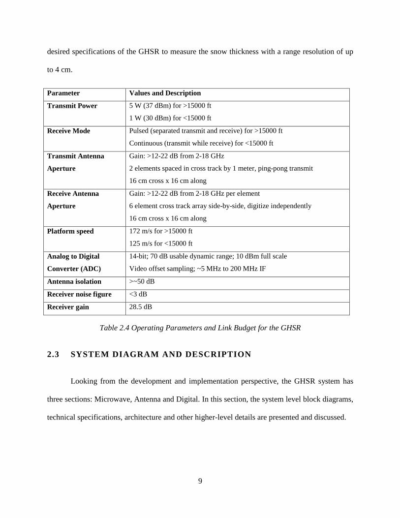
9
desired specifications of the GHSR to measure the snow thickness with a range resolution of up
to 4 cm.
Parameter Values and Description
Transmit Power 5 W (37 dBm) for >15000 ft
1 W (30 dBm) for <15000 ft
Receive Mode Pulsed (separated transmit and receive) for >15000 ft
Continuous (transmit while receive) for <15000 ft
Transmit Antenna
Aperture
Gain: >12-22 dB from 2-18 GHz
2 elements spaced in cross track by 1 meter, ping-pong transmit
16 cm cross x 16 cm along
Receive Antenna
Aperture
Gain: >12-22 dB from 2-18 GHz per element
6 element cross track array side-by-side, digitize independently
16 cm cross x 16 cm along
Platform speed 172 m/s for >15000 ft
125 m/s for <15000 ft
Analog to Digital
Converter (ADC)
14-bit; 70 dB usable dynamic range; 10 dBm full scale
Video offset sampling; ~5 MHz to 200 MHz IF
Antenna isolation >~50 dB
Receiver noise figure <3 dB
Receiver gain 28.5 dB
Table 2.4 Operating Parameters and Link Budget for the GHSR
2.3 SYSTEM DIAGRAM AND DESCRIPTION
Looking from the development and implementation perspective, the GHSR system has
three sections: Microwave, Antenna and Digital. In this section, the system level block diagrams,
technical specifications, architecture and other higher-level details are presented and discussed.

10
Figure 2.3 Simplified Top-level Block Diagram of the GHSR
The top-level simplified block diagram, shown in Figure 2.3, shows the most relevant
sections and sub-sections of the GHSR. The digital section deals with the waveform generation,
generation and distribution of system clock signals, data acquisition, storage and radar control
software. The microwave system includes the hardware for transmitter and receiver units
developed on printed circuits boards and modular drop-in components. The radar signal
transmission and reception are accomplished by means of 2 and 8 units of Vivaldi antenna
elements, respectively. The number of antenna elements can be varied depending on the
platform. A more detailed block diagram is shown in Figure 2.4.

11
Figure 2.4 Detailed System Block Diagram of the GHSR (illustration courtesy John Paden)
Figure 2.4 was developed to support operation on different platforms. For the Global
Hawk platform, the server, switches and GPS antenna are not required as they are provided via
the remote C3 link, GPS, flight data and power through the EIP #6. On the manned platforms, P-
3B and C-130, these are necessary in addition to the temperature control system.
The central timing unit (CTU) maintains control and timing, synchronization and system
monitoring. The Arbitrary Waveform Generator (AWG) unit has two Digital-Analog Converters
(DAC) and generates the chirps for the next x16 multiplication stage. Data Acquisition (DAQ)
units have Analog-Digital Converters (ADC) to sample the waveform from each IF board in the
set of receivers. The SYNC Distribution unit is capable of driving 8 units. The SYNC signals
from the CTU are distributed to the units denoted as AWG and four 2-channel DAQ units (1

12
through 4). All these units, except the SYNC distributor unit, are also connected to the network
switch for remote control and monitoring. The GPS/Time and sensors are connected to the CTU.
The clock distribution network provides all the clocks required by the digital modules and the
frequency multiplier in the MW system.
The chirp signals from the AWGs are fed to the two 16-times frequency multiplier (x16)
units. One of the x16 frequency multiplier output is transmitted after power amplification in the
last stage through 2 Vivaldi antenna arrays in an alternating or ping-pong fashion. Another
output is forwarded to the 8 receiver units by a 1:8 Reference local oscillator (LO) distribution
network. The eight-receivers receive the backscattered signal from a system of 8 Vivaldi antenna
arrays. The down-converted IF signal from the RF-PCBs in each Receiver is fed to the
corresponding channel for data sampling. Data from DAQ modules are written to the on-board
storage system.
2.4 DIGITAL SYSTEM
2.4.1 CLOCK SIGNALS
The clock generation subsystem starts from a base reference GPS-disciplined oscillator to
feed a 100 MHz phase-locked oscillator (PLO). The distribution network is derived from that
signal to drive all the modules and the MW system that require 500 MHz, 2400 MHz and 38
GHz clocks. The block diagram of the distribution network is depicted in Figure 2.5.

13
Figure 2.5 Block diagram of the clock signal generation and distribution
A generic GPS combined with an inertial measurement unit (IMU) component receives
the accurate positioning and provides the reference 10 MHz for the Wenzel 501-23588 Standard
100 MHz-Stress Compensated PLO. The 10 MHz GPS-discipline reference and 100 MHz PLO
are ultra-low phase noise components and thus do not set the phase noise floor of the system.
The output signal is typically 13 dBm driving a Mini-Circuits power splitter.
A custom Frequency Synthesizer was designed at CReSIS to generate the reference
signals at 500 MHz and 2400 MHz. Specifically; it provides the 500 MHz clock to the DAQ 1 to
4 modules, 2400 MHz clock to AWG 1 to 2 modules and 2400 MHz to Stage-0 of the x16
frequency multiplier. The form factor is similar to that of a commercial PLO except that it is
programmable and uses an HMC833LP6G Phase-Locked Loop (PLL) for the 2400 MHz sources
and an Analog Devices ADF4351 PLL for the 500 MHz source. This part uses a 100-pin Thin

14
Quad Flat Pack (TQFP) Xilinx XC95144XL-10TQ100I CPLD IC for programming the PLL with
integrated Voltage Controlled Oscillator (VCO). A programmable JTAG header lets the user
program the respective VHDL code to tune (integer or fractional) to a desired frequency. The
HMC833’s supported range is from 25 MHz – 6000 MHz though the fundamental range is 1500
MHz – 3000 MHz. The ADF4351’s supported frequency range is 35 to 4400 MHz with a
fundamental frequency range of 2200-4400 MHz. The ADF4351 is used for the 500 MHz signal
because it supports phase locking to the divided output, which the HMC833 does not support.
These units use a Peregrine PE43205 digital step attenuator to support different output power
levels. A Mini-Circuits RF power splitter for each frequency distributes the output to respective
modules.
For the x16 frequency multiplier, a 38 GHz PLO is necessary for the last down-
conversion stage. This is locked to the external 100 MHz reference signal. This Microwave
Dynamics PLO-2070 38.00 is a Phase-Locked Dielectric Resonator Oscillator with a typical
output of 16 dBm with phase noise dependent on input phase noise [26].
2.4.2 DIGITAL MODULES
The digital system modules in the GHSR generally refer to the Remote Sensing Solutions
(RSS) Arena modules that support the CTU, AWGs and DAQs. RSS designed and manufactured
these modules. The CTU module has a Xilinx system-on-chip (SoC) Zynq-7030 and the AWG
and DAQ modules have a Zynq-7045. The Zynq includes a dual-core ARM Cortex-A9
processor. All the modules have this XC7Z030-3FFG676E (or XC7Z045-3FFG676E) and
support for one (CTU) or two (DAQ and AWG) daughter boards through a proprietary
mezzanine connector. Different daughter boards or mezzanine cards support control and timing,

15
waveform generation and data acquisition. The advantage of this configuration is one base
module supporting external memory, high-speed programmable logic and processing system can
be repeated for CTU, AWGs and DAQs with suitable Mezzanine cards. The SYNC Distribution
is a 1:8 module and can be daisy-chained for more than 8 slave modules for synchronization.
The arena modules run an Embedded Linux Kernel 3.2 booted at the time of startup from
an SD card with preloaded bootable images. The modules are connected to the network switch
and have a dedicated IP address for remote control. The enclosures are conductively cooled and
support DC voltage from 8 V to 28 V. The modules support a wide operating temperature range
from 0 C to +70 C and high altitude operation up to 70,000 ft.
The Central Timing Unit (CTU) is technically called the Control and Timing Module
(CTM) with a Control Signal and Time Synchronization Expansion Mezzanine Card. This
module supports 12 single-ended TTL outputs and 12 single-ended TTL inputs. These can be
connected to different components like voltage and temperature sensors for receiving feedback
and to send control signals. The CTU has a dedicated single ended PPS input and an RS-232
input for recording the GPS stream. The CTU takes the 10 MHz clock from the GPS/Time unit.
The Arbitrary Waveform Generator (AWG) is a single channel 2.5 GSPS D/A Mezzanine
Card. The DAC IC is an Analog Devices AD9129 for direct RF synthesis supporting different
modes: baseband, 2x interpolation and mix-mode. The input clock is a ±3dBm 2400 MHz sine
wave from the frequency synthesizer referred to as 2400 MHz PLO. This clock is required to be
a multiple of 80 MHz for synchronization. AWG 1 and AWG 2 generate the 100 MHz – 1100
MHz chirp for the Stage_0 section of the x16 frequency multiplier.

16
The Data AcQuisition (DAQ) module is a dual channel 14-bit 500MSPS A/D Mezzanine
Card. The two ADC ICs are Intersil ADC-ISLA214P50 to sample the IF channels from the
receiver. The input ports can accept a maximum of 2V peak-to-peak signal (10 dBm) and support
up to 700 MHz video bandwidth. The input clock is a ±3dBm 500 MHz sine wave from the
frequency synthesizer referred to as 500 MHz PLO.
Miscellaneous parts include sensors, storage, switch, server and radar control software.
The sensors that are connected to the CTU are able to report either voltage or temperature. The
data from the DAQ modules is written to on-board solid-state storage. A standard rugged
network switch and server are connected to the RSS modules. The server runs the radar control
software essential to run and control the modules. On the Global Hawk platform, the server
remotely accesses the RSS modules through the C3 link.
2.5 MICROWAVE SYSTEM
2.5.1 X16 FREQUENCY MULTIPLIER
On the transmitter side, the 100 MHz – 1100 MHz chirp from the arbitrary waveform
generator in the digital system is converted to the 2 GHz – 18 GHz chirp for transmission by
successive frequency doubling stages and a down-conversion stage. Stage_0 up-converts the
100-1100 MHz baseband signal to the 2500-3500 MHz range. This stage utilizes the 2400 MHz
clock from the frequency synthesizer referred to as 2400 MHz PLO. This upconversion utilizes
an I-Q mixer for better image rejection. Stage_0 is a separate module design with SMT filters,
90° hybrid coupler and wire-bonded I-Q mixer. The output of this stage is fed to the main
multiplier chain. The 2.5-3.5 GHz chirp is then multiplied 16 times up to 40-56 GHz and mixed
with 38 GHz to generate the final 2-18 GHz chirp. The down conversion utilizes a signal from

17
the Microwave Dynamics PLO, which is locked to a 100 MHz reference. The multiplier chain is
a modular design using the drop-in technology of X-Microwave, which was identified as a
suitable format to eliminate connectorized components and enable future board-level integration
[27]. More details on the frequency multiplier are provided in the Chapter-3
2.5.2 RECEIVER (REF LO DIST., RF PCB, IF PCB)
While one output of the x16 frequency multiplier is transmitted, the other output is
distributed to the 8 receivers by a 1:8 reference LO distribution board. The Receiver consists of
the RF PCB on which the received signal from the antenna is down-converted by the reference
LO to produce the beat frequency or the IF signal. The IF PCB switches the signal to the
corresponding filter section depending on the mode of operation and conditions the signal to be
sampled by the DAQ modules.
2.5.3 TRANSMITTER
The transmitter handles switching the RF transmission between transmit antennas and
blanking the transmitter during reception when in pulsed mode.

18
2.6 ANTENNA SYSTEM
Figure 2.6 Antenna Slice
The basic building block of the antenna system is referred as a ‘slice’. Each slice is a
16x1 Vivaldi array adapted from the design by S. Yan et al. [28] [15] driven by the 1:16 power
divider built into the slice. Each slice is driven by one signal fed by an SMA connector as shown
in Figure 2.6. The dimensions of each slice are 6.7 inch along-track and 7.5 inch tall (+ 0.75 inch
for power divider). The orientation of every slice is in the along-track and the thickness is 1 cm
in cross-track.
The 16x16 Vivaldi array is formed by parallel placement of sixteen Slices along the
cross-track as shown in Figure 2.7. This array of 16x16 elements is a single antenna element to
the radar system. The antenna dimensions are 6.7 inch along-track x 7.5 inch tall (+0.75 inch for
power divider) x 16 cm in cross-track. Another power divider connected through the RF cables
drives the 16 ports of the antenna.

19
Figure 2.7 Antenna 16x16
The antenna placement is illustrated in Figure 2.8. Two transmit antennas operate in
ping-pong mode for transmission. Their placement is aligned with the outer edges of the 8
receiving antennas. The associated power amplifier for the transmit antennas and low-noise
amplifiers (LNAs) for the receive antennas are built into the power divider enclosures. Eight
antennas arranged in the cross-track in either straight or staggered configuration operate as
receivers.

20
Figure 2.8 Antenna placement configurations for GHSR: (top) straight configuration; (bottom) Staggered configuration.

21
2.7 SUMMARY OF IMPROVEMENTS RESULTING THIS WORK
The overview of the GHSR in this chapter outlines the improvements from the previous
designs. Distinguishing features are the remote operation and support for altitudes from 700 ft to
70,000 feet. The GHSR is much lighter in weight and a more rugged design compared to
previous units. The Radar Control Software supports remote control during flight. The Digital
system implemented by arena modules brings a new level of flexibility in CReSIS radars for
waveform generation and acquisition. The frequency multiplier system employs a modular
design and custom-designed microwave and millimeter wave filters. The development of this
radar led to the study of different filter topologies and technologies and to the implementation of
a computer-aided-manufacturing (CAM) process to fabricate them in house.

22
CHAPTER 3 FREQUENCY MULTIPLIER
3.1 PREVIOUS WORK
As mentioned in Chapter 1, the signal generator for the snow radar system has been
progressively upgraded from a yttrium iron garnet (YIG)-based circuits [7] to a voltage
controlled oscillator (VCO)-based system [11], then to a DDS/multiplier based system [13] [20];
and ultimately to the current AWG/multiplier based system. A review of the different frequency
synthesis techniques is documented in [29] while a summary of the different versions of the
snow radar and the multiple upgrades to the chirp generators is given in Yan et al. [20].
Chirp generation for radar using a digitally-generated baseband signal and frequency
multiplication has been documented in the literature [30] [18] [31]. The main advantages with
respect to earlier analog VCO-based and YIG-based systems include the ability to generate faster
sweeps and to pre-distort the signal phase and amplitude to reduce range side lobes. The
DDS/frequency multiplier technique was demonstrated by Gomez-Garcia et al. [13] to generate
2-8 GHz and 12-18 GHz for the snow, and Ku-band altimeter, respectively. A 1.5-2.25 GHz
baseband chirp is multiplied 8 times to 12-18 GHz, which is used as the transmit signal for the
CReSIS altimeter. When mixed down with a phase-locked 20 GHz source, the resulting 2-8 GHz
chirp is used as the transmit signal for the snow radar. The multiplication is done by cascaded
stages of x4 and x2 frequency multipliers accompanied by amplifiers, attenuators and band-pass
filters. The combination of multiple filters used each stage resulted in a steep roll-off with a non-
linear group delay that increased as the signal propagated through each stage. This frequency
non-linearity is corrected by a linearization method [13]. This system was successfully deployed

23
numerous times on different platforms such as the P-3B, DC-8, and Twin Otter as part of NASA
OIB and CReSIS NSF missions [20].
In 2015, a similar system was designed to generate 2-18 GHz chirp by multiplying a
baseband chirp from 1.375-2.375 GHz using a 16 times multiplication chain [14]. The original
design featured a cascade of x4, x2 and x2 multipliers with suitable amplification, attenuation
and filtering in each stage as seen in Figure 3.1. The multiplied chirp 22-38 GHz is then down-
converted to the 2-18 GHz band using a mixer driven by a phase-locked 20 GHz signal. The
design was revised to replace the first x4 multiplication stage by two x2 multiplication stages and
the frequency of the down-conversion LO was changed from 20 GHz to 40 GHz to improve the
spectral purity of the signal ( [32] and [15]). This multiplier flew on a Twin Otter and Basler
platforms as part of U. S. Naval Research Laboratory (NRL) and Alfred Wegener Institute
(AWI) missions. We observed that the side lobe performance is sensitive to time delays and
reflections between stages so it is important to choose the inter-stage padding and adapters
carefully. While this design offered a functional signal generator, it suffered from coherent noise
due to in-band-harmonics [14]. The final 2-18 GHz chirp includes the intermodulation products
produced by the x4 frequency multiplier in the first stage of the x16 multiplication chain
resulting in frequency non-linearity. [14]. The frequency non-linearity and reflections in between
the components resulted in range side lobes [14]. These reflections can cause the short-range
leakage responsible for increasing the residual phase noise of beat frequency signal above the
system noise floor [33].

24
Figure 3.1 DDS-based 2-18 GHz frequency multiplier
3.2 PROPOSED DESIGN
The design and deployment of the previous multiplier chains helped in the identification
of issues that could be improved in the next design cycle. The idea behind utilizing the frequency
multiplication for GHSR is to generate the 2-18 GHz from the base band chirp of 100-1100 MHz
available from the AWG. There is a significant influence of previous designs in the new modular
non-connectorized components for GHSR x16 frequency multiplier.
3.2.1 IMPROVEMENT OF SPECTRAL PURITY
One important feature of the GHSR x16 frequency multiplier is keeping the harmonics
always out of band at each multiplication stage. The 16 times multiplication is done by four
cascaded stages of x2 multipliers. The final goal to achieve the 16 GHz bandwidth by doubling
the bandwidth at each stage. In order to keep the third-order products outside the required band,
the baseband frequencies toned to be chosen carefully.

25
Let us denote the base band chirp sweeps from f_LOW to f_HIGH. The frequency
components at the output of x2 multiplier has the fundamental band (f_LOW - f_HIGH), the required
second order band (f_x2_LOW - f_x2_HIGH), the undesired third order band (f_x3_LOW - f_x3_HIGH)
and other higher-order frequency bands. The pictographic representation is provided in Figure
3.2. Every multiplier has a substantial amount of fundamental and higher band leakage that
require the use of sharp band-pass filters to eliminate frequency components outside the band of
interest..
Figure 3.2 Pictographic representation of the frequency bands in a multiplier
The non-overlapping frequency bands can be calculated by substituting the values for the
higher order bands in terms of baseband terms. This is summarized in Table 3.1.
Term f_x2_LOW f_x2_HIGH f_x3_LOW f_x3_HIGH f_HIGH
Equivalent 2 × 𝑓𝑓_𝐿𝐿𝐿𝐿𝐿𝐿 2 × 𝑓𝑓_𝐻𝐻𝐻𝐻𝐻𝐻𝐻𝐻 3 × 𝑓𝑓_𝐿𝐿𝐿𝐿𝐿𝐿 3 × 𝑓𝑓_𝐻𝐻𝐻𝐻𝐻𝐻𝐻𝐻 𝑓𝑓_𝐿𝐿𝐿𝐿𝐿𝐿 + 1 𝐺𝐺𝐺𝐺𝐺𝐺
Table 3.1 Parameters for Non-overlapping frequency bands
From the Figure 3.2 conditions for the non-overlapping bands are summarized in Table 3.2. The
terms are substituted with their equivalents for calculation.
Fundamental and Second harmonic Second and Third harmonic
𝑓𝑓_𝑥𝑥2_𝐿𝐿𝐿𝐿𝐿𝐿 > 𝑓𝑓_𝐻𝐻𝐻𝐻𝐻𝐻𝐻𝐻
2 × 𝑓𝑓_𝐿𝐿𝐿𝐿𝐿𝐿 > 𝑓𝑓_𝐻𝐻𝐻𝐻𝐻𝐻𝐻𝐻
𝑓𝑓_𝑥𝑥3_𝐿𝐿𝐿𝐿𝐿𝐿 > 𝑓𝑓_𝑥𝑥2_𝐻𝐻𝐻𝐻𝐻𝐻𝐻𝐻
3 × 𝑓𝑓_𝐿𝐿𝐿𝐿𝐿𝐿 > 2 × 𝑓𝑓_𝐻𝐻𝐻𝐻𝐻𝐻𝐻𝐻

26
2 × 𝑓𝑓_𝐿𝐿𝐿𝐿𝐿𝐿 > 𝑓𝑓_𝐿𝐿𝐿𝐿𝐿𝐿 + 1 𝐺𝐺𝐺𝐺𝐺𝐺
𝑓𝑓_𝐿𝐿𝐿𝐿𝐿𝐿 > 1 𝐺𝐺𝐺𝐺𝐺𝐺
3 × 𝑓𝑓_𝐿𝐿𝐿𝐿𝐿𝐿 > 2 × 𝑓𝑓_𝐿𝐿𝐿𝐿𝐿𝐿 + 2 𝐺𝐺𝐺𝐺𝐺𝐺
𝒇𝒇_𝑳𝑳𝑳𝑳𝑳𝑳 > 𝟐𝟐 𝑮𝑮𝑮𝑮𝑮𝑮
Table 3.2 Calculation of Non-Overlapping frequency bands
Therefore, the desired condition in our design is that the lower end of the chirp has to be
greater than 2 GHz to keep the higher-order harmonics out of the desired band. We thus chose
2.5 GHz – 3.5 GHz, which fulfils these criteria. The AWGs can generate such signal in the so-
called mix mode but is not preferred because direct RF synthesis cannot generate the 2.5-3.5
GHz in baseband mode. A much feasible band for generation of the baseband chirp is the 0.1-1.1
GHz, which can be converted to the 2.5-3.5 GHz range by using a mixer driven by a 2.4 GHz
phase locked signal. This initial up-conversion stage is denoted tage_0. Stage_0 also uses a
quadrature hybrid coupler and an In-phase/Quadrature (IQ)-mixer to provide higher image
rejection, thereby relaxing the band-pass filter requirements at the output of this stage.
3.2.2 SIZE REDUCTION AND INTEGRATION
Another design factor is driven by the desire to avoid using connectorized components as
much as possible. This helps reduce the effects of reflections between components. For the
previous multiplier chains implemented using connectorized components, these reflections often
fall within the range resolution of the radar and can be observed in the system response. To
minimize the length of chain, reduce the reflections and also obtaining a smaller size and lower
weight (all desired attributes of a UAV-borne system), surface-mount technology was chosen
over heavy connectorized units. This also enables future integration into a single PCB design that
is highly integrated. Suitable components were identified after choosing the baseband frequency.
The criteria for component selection is explained in Section 3.4 DESCRIPTION AND
IMPLEMENTATION OF INDIVIDUAL MULTIPLIER STAGES. After the component

27
selection was finalized, a spectral-domain simulation was done in Genesys Spectrasys to analyze
the contribution and propagation for the chirp signal and its harmonics, noise, attenuation and
other characteristics. Spectrasys utilize the Spectral Propagation And Root Cause Analysis
(SPARCA) technique [34] to perform this analysis. Though complete non-linear models for the
mixers and multipliers are not always available, this type of simulation helps to study the effects
of harmonics and reflections encountered in the chain.
Figure 3.3 X16 Frequency Multiplier Block Diagram
The top-level block diagram of the new implementation is provided in Figure 3.3. In
addition, a set of active modules require DC power supplied by the power distribution board
described in Section 3.5. Integration of the DC-bias circuitry and active analog components is a
crucial part of the project because of surface mount components, drop-in modules, wire-bondable
dies, different custom filters and launches. Unlike in the previous connectorized
implementations, integration is a more challenging task to be addressed in the early stages of the
design. Integration aspects of this project are further discussed in Section 3.6.

28
3.3 SYSTEM LEVEL SIMULATIONS
An RF simulation for the multiplication stages and down conversion provides a sight into
the harmonics, intermodulation products and suppression of undesired products by filters. As
discussed in Section 3.2 PROPOSED DESIGN this part of the project was completed through
the tool Spectrasys from Keysight Technologies. Figure 3.4 shows the block diagram of the
complete frequency multiplier configuration simulated using Spectrasys.
Figure 3.4 Spectrasys schematic for sytem level simulation of the frequency multiplier
First, we performed a preliminary selection of frequency multipliers that were
commercially available in either chip or die format. For each frequency double, we entered the
typical conversion gain, output harmonic levels, return losses and input drive levels from the
manufacturer. Amplifiers gain and/or attenuators are included to reach the required nominal
inputs of subsequent stages. Band pass filters were synthesized separately by the M/FILTER tool

29
in Genesys to get the required out-of-band rejection after each multiplication stage to reduce
spurious content being fed to subsequent stages. S-parameter datasets for the filters (touchstone
files) were used instead of idealized responses.
Two types of analysis were performed, namely for a wide-band input and for a
monotonic input. First simulation used a source that excites the system with 2.5 – 3.5 GHz chirp.
The second simulation uses five uniformly spaced monotones at 2.5, 2.75, 3, 3.25 and 3.5 GHz.
Figure 3.5 Spectrasys Schematic Response for wide-band chirp
The final stage response of the simulation producing 2 – 18 GHz chirp with a wide band
source is given in Figure 3.5. The node noise is the individual contribution of the attenuator
adjacent to the output (port 3), where the spectrum is measured. The response clearly shows the
desired 2 – 18 GHz chirp produced from the ideal source. Next, this was crosschecked with the
monotonic response at 5 discrete points. The outputs for the monotonic input is given in Figure
3.6.

30
Figure 3.6 Spectrasys Response for baseband monotone excitation
The power levels for both type of analyses are summarized and compared in Table 3.3.
The values are close for monotone and wide band responses. This Spectrasys simulation was
helpful to ensure the frequency plan and components can be relied up on before procuring. The
restriction for the filters can be visualized by the node responses at the stages in between.
Wideband Excitation Monotone Excitation
Frequency, GHz Output Power, dBm Output Power, dBm
2 -2.98 -2.979
6 -0.426 -0.431
10 +0.993 +0.991
14 -0.451 -0.456
18 -2.947 -2.946
Table 3.3 Summary of simulated output power levels for wide band and monotone excitation

31
3.4 DESCRIPTION AND IMPLEMENTATION OF INDIVIDUAL
MULTIPLIER STAGES
A description of the implementation of the each frequency translation stage (denoted
Stage_0 through Stage_4, and Mixer, respectively) is presented in this section. We chose the best
components available at the time of design and a technical justification for the selection of
almost every part is given, including any trade-offs made during the design. We also give
recommendations for future upgrades in cases where a newer part with better performance has
become available.
3.4.1 FIRST UP-CONVERSION STAGE: STAGE_0
Figure 3.7 Block diagram of the frequency translation Stage_0

32
3.4.1.1 CIRCUIT OVERVIEW
The first up-conversion stage is denoted Stage_0, and is depicted in the Figure 3.7. It is
implemented on a 30-mil Rogers 4350B PCB (εr=3.66) to support incorporation of all the
surface-mount components. It takes the inputs from an edge-launch MCX female connector
(73415-1061 from Molex Inc.) These connectors can be installed flushed against the PCB by
placing a cutout in the PCB design mentioned in Section 3.4.1.2. This facilitates the Stage_0 to
be dropped into an enclosure without protruding connectors. AWG and 2.4 GHz PLO inputs also
use MCX male connector on their side.
Internal to this stage, the input from AWG is filtered by a CReSIS-designed, custom
lumped-element 0.1 – 1.1 GHz band-pass filter before feeding it to the hybrid coupler. A
standard SMT placement layout of 2 x 0.5 inch was decided to develop these filters. This is
compatible with commercial industry filter designs. The commercial filters often use the plated
edges at the ports. The current version of CReSIS filters uses a 3x3 via feed for the ports.
Another option is to remove this via-feed and use a copper strip feed from the trace on the SMT
filter base. The filter base is a 30-mil RO-4350 substrate with lumped elements. The values are
first synthesized from in AWR Design Environment. A composite layout from Gerber files
generated in Altium designer is exported to ADS for co-simulation. The complete design is
optimized here before fabrication. A more detailed note is provided in Chapter - 4 on Filter
Design.
The hybrid coupler (Werlatone QH10245) generates two coupled outputs with In-phase
and quadrature components. Due to the unavailability of a coupler in desired frequency range,
this was a custom design from Werlatone. The Isolation port is terminated with a 50 Ohm chip

33
resistor to ground (Anaren R2B131350R0J5L0 SMT). The coupled phase-shifted outputs are fed
to the I-Q up-converter (Marki MLIQ-0218LCH-2) where they are mixed with 2.4 GHz phase-
locked signal. The 2.4 GHz signal is filtered by a band-pass filter (Mini-Circuits CBP-2400A+).
The mixer is a die that was wire-boned to the signal traces. This was done at High Density
Electronics Center at University of Arkansas.
In terms of attenuation, the Mini-Circuits RCAT pads have a good performance at the
desired frequencies and they come in surface-mount format, supporting attenuation from 1-10
dB. The I-Q mixer has acceptable return losses at all its ports. Instead of the SMT attenuators on
the traces, using a die attenuator close to mixer would improve the performance by further
reducing reflections. To this end, we chose TriQuint’s (now Qorvo) wideband attenuators
(TGL4201). The smaller size 20 x 20 mil helps the die to be placed right next to the ports of the
370 x 160 mil I-Q mixer.
The up-converted signal at the output of the mixer is filtered a custom lumped 2.5 – 3.5
GHz band-pass filter (Lark Engineering XMS3000-U1000-10CC). Finally, the 2.5-3.5 GHz chirp
is sent to output port with a SMP Male connector (Rosenberger 19S202-40ML5). SMP
connectors are well suited for operation in this frequency range, providing a coaxial pin diameter
adequate to land on planar transmission line used in thex16 chain build. The Stage_0 is
connected to the x16 chain by a female-female (“bullet”) connector.
3.4.1.2 IMPLEMENTATION
As the Stage_0 bridges the AWG output of 0.1 – 1.1 GHz chirp to the frequency
multiplier, we developed a printed circuit board (PCB) using Altium Designer. The top view of
the three-dimensional (3D) model from Altium is shown in Figure 3.8.

34
Figure 3.8 Top view of the 3D-rendered PCB for Stage_0 implemented in Altium Designer
The Stage_0 board is implemented on 30 mils thick Rogers 4350B with 1 oz electro
deposited (ED) copper on both sides. This substrate can be handled easily after mounting the
heavy hybrid and three filters. The dielectric constant used in the design process (εr) was 3.66
and the dissipation factor was 0.0031. Grounded co-planar waveguide (CPWG) traces was
chosen. The selection of a suitable trace width and gap was based on the tolerances provided by
the board manufacturing companies. A width of 43 mils and with a 10 mils gap was chosen to
provide a 50-Ohm characteristic impedance. Initially, the plan was to use different CPWG
configurations for inputs (RF and LO) and output due to frequency dependent impedance.
Theoretically, the 43 mils wide signal trace and 10 mils gap would provide impedances closer to
50 ohms for three different frequency ranges for a resolution about 1 mil.
35
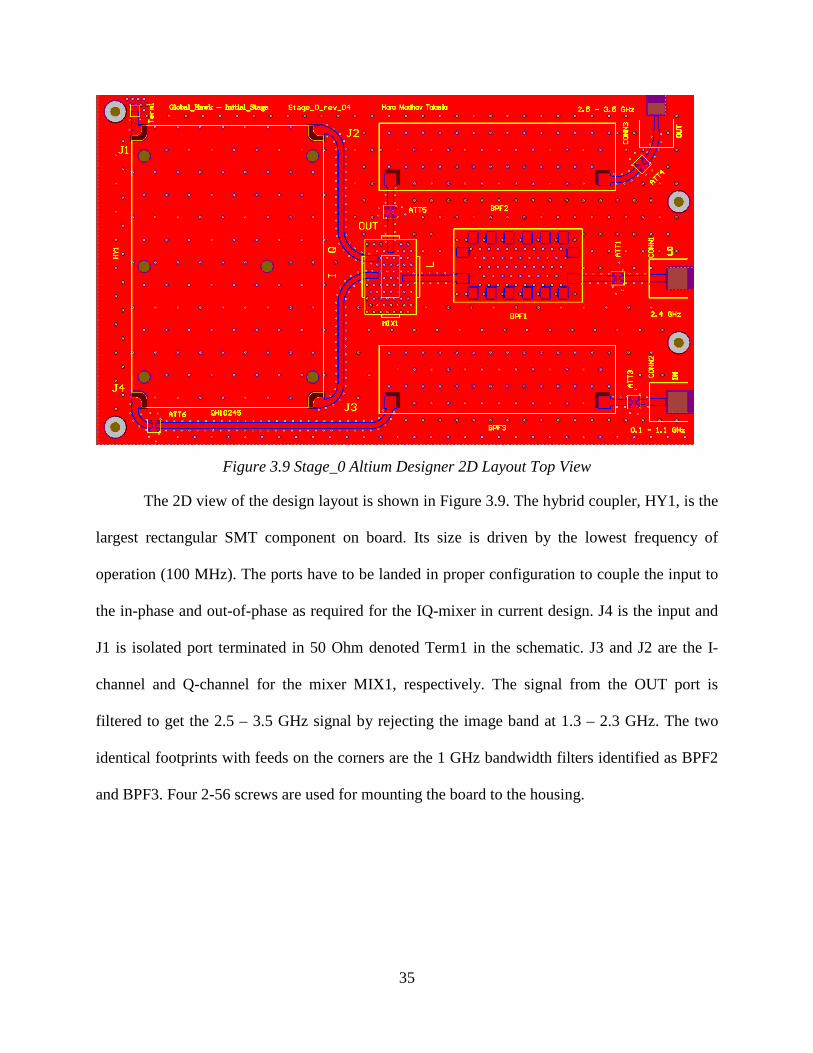
Figure 3.9 Stage_0 Altium Designer 2D Layout Top View
The 2D view of the design layout is shown in Figure 3.9. The hybrid coupler, HY1, is the
largest rectangular SMT component on board. Its size is driven by the lowest frequency of
operation (100 MHz). The ports have to be landed in proper configuration to couple the input to
the in-phase and out-of-phase as required for the IQ-mixer in current design. J4 is the input and
J1 is isolated port terminated in 50 Ohm denoted Term1 in the schematic. J3 and J2 are the I-
channel and Q-channel for the mixer MIX1, respectively. The signal from the OUT port is
filtered to get the 2.5 – 3.5 GHz signal by rejecting the image band at 1.3 – 2.3 GHz. The two
identical footprints with feeds on the corners are the 1 GHz bandwidth filters identified as BPF2
and BPF3. Four 2-56 screws are used for mounting the board to the housing.

36
Figure 3.10 Spacing limits for Via-Shielding on Stage_0 PCB
Connection between the top and bottom ground planes is done through plated via holes
with10 mil diameter. The hybrid coupler and other open areas have via stitching for the ground
net with a 200 mil spaced staggered grid. The filters, BPF2 and BPF3, have a similar grid with
150 mil spacing. BPF1 has an 80 mil grid because of the isolated ground pad under the filter.
Mixer area has 60 mil grid that supports the die and is exposed without solder mask. The
different grid dimensions are used to get extra lines of staggered vias under the footprints of
components. The signal traces are shielded by 50 mil spaced ground vias. This shield is more
than adequate for all the frequencies from 0.1 – 3.5 GHz on this stage. The minimum spacing
between the vias of shield should be less than the 1/20 of the wavelength at the highest operating
frequency. Figure 3.10 shows a plot of the required spacing as a function of frequency
(APPENDIX: via_shield.m) for the range of interest. For 3.5 GHz the minimum spacing required
is 88 mils, which is satisfied with the 50-mil spacing.

37
Figure 3.11 Stage_0 Mixer and pads placement for Wire-bonding: (left) CAD model and (right) photograph of the mixer chip installed on the board.
The left-side of the Figure 3.11 and Figure 3.12 is provided as a guide for the wire-
bonding facility and result is on the right-half. The mixer outline was obtained datasheet [35],
and the three attenuators (color-coded to red and sky-blue denoting 3dB and 2 dB pads,
respectively) were drawn to scale. The signal trace, pad and mixer port are bonded by a 1-mil
diameter pure gold wire in a ground-signal-ground (g-s-g) configuration as shown in Figure 3.12.
This g-s-g technique is employed on all the ports of the mixer chip.

38
Figure 3.12 Stage_0 Wire-bonding g-s-g configuration: (left) diagram (right) photograph
Reflow procedures are to be addressed carefully during implementation. First, the PCB is
sent to the wire-bonding facility to finish the links for the mixer and attenuator pads. Bulky
components like filters and hybrid are populated next. After confirmation of the alignment,
RCATs and resistor are next in the queue. This procedure needs the board to run several times
through hot-air reflow machine. The conventional solder paste in the lab has needs higher
temperature profiles up to 400 degrees Celsius. However, because of the sensitivity of wire-
bonds and different solder paste, current custom profile that uses much lower temperature was
implemented.
The solder paste from Nordson EFD LLC, 7020199, of the family No Clean (NC)
labelled NC-501A is used for Stage_0 reflow. The composition is 62 % Tin (Sn), 36 % Lead
(Pb) and 2% Silver (Ag) constituting 88% metal. The boiling temperature range is 1240 – 1980 C
giving advantage of low temperature reflow. The remains after soldering do not need to be
cleaned by any other solutions. Next, the connectors are manually soldered in the cutouts.

39
Finally, the finished board is placed and tightened inside the enclosure with openings near the
ports to accommodate any adapter or cable for MCX and SMP.
3.4.2 X16 FREQUENCY MULTIPLICATION CHAIN
Figure 3.13 X16 Chain Diagram

40
3.4.2.1 DESIGN OVERVIEW
The complete X16 frequency multiplication chain is presented in Figure 3.13, which
includes a pre-amplification stage to feed the first multiplier with sufficient input power. The
design of the chain is mainly dependent on the selection of the separate frequency doubling
stages. The output of each stage required a custom band-pass filter for spurious suppression.
Table 3.4 gives a summary of the frequency stages from 1 through 4 with relevant multiplier
parameters.
Parameter Stage – 1 Stage – 2 Stage – 3 Stage – 4
Frequency 5 – 7 GHz 10 – 14 GHz 20 – 28 GHz 40 – 56 GHz
Filter Type Interdigital cavity Interdigital cavity Planar on
alumina substrate Planar on alumina substrate
Multiplier Macom XX1002-QH
Hittite (Analog) HMC573LC3B
Hittite (Analog) HMC576
Hittite (Analog) HMC1105
Package SMT SMT Die Die
RF Input (dBm) 0 (-3:3) 4:6 (-2:8) 2:6 (0:6) 13 (15)
Fundamental Suppression (dBc) -30 -20 -20 -35
Output (dBm) 16 12 (14) 15 (16:17) Input - 12
Third Harmonic Suppression (dBc) -25 -25 -17 -30
Type (Power) Active Active Active Passive
Table 3.4 Summary of relevant parameters for each stage in the X16 frequency multiplier
The pre-amplification stage employs a series of surface-mount amplifiers (Mini-Circuits
PMA3-83LN+) providing approximately 21.5 dB gain in the 2.5 – 3.5 GHz range. The

41
attenuators are from the Mini-circuits RCAT series, and their values were adjusted to maintain
the required input drive for the first multiplier.
The band pass filter at the output of the first multiplication stage (Stage 1) is an
interdigital cavity filter designed and fabricated at CReSIS. The ports are hermetically sealed and
the launch pins land on the traces of the X-Microwave modules. Suppression of the fundamental
and third harmonics from the first multiplier is given proper attention. The RCAT attenuators in
Stage – 1 are chosen to adjust the power level for next stage. The bandpass filter at the output of
Stage – 2 also is likewise an interdigital cavity filter machined in-house. The bandpass filters for
the output of Stage – 3 and Stage – 4 are edge-coupled micro-strip filters with coplanar
waveguide feeds, which were manufactured on 5-mil Alumina substrate. The specifics on the
design and performance of these filters will be given in Chapter - 4. The inclusion of attenuators
and filters causes more loss and the output of Stage – 3 multiplier is not enough to provide
sufficient power for Stage – 4 multiplier. An extra amplification module is added here to boost
the power of the chirp signal. Every unit is a die and is wire-bonded on modules. The x16 chain
ends by feeding the 40-56 GHz chirp to a down-converter to produce the final 2-18 GHz chirp.

42
Figure 3.14 Typical layout grid and landing of X-Microwave modules (from ref [27])
3.4.2.2 IMPLEMENTATION
The components in the x16 chain, the down-converting mixer and the pre-amp section are
all part of a single integrated module. Highly integrated modules have been reported in the
literature [36]. We chose an interconnection technique developed by X-Microwave [37] in which
each component is placed in to a drop in module and integrated into a grid with tapped mounting
holes. A general layout picture is provided in Figure 3.14.

43
Figure 3.15 X-Microwave Probe landing on module
The modules are tested using a coaxial probe (XM-PB1-185F) shown in the Figure 3.15
that has signal pin landing at an angle on module’s signal trace. The connector on other end of
probe is 1.85 mm female connector (XM-PB1-185F) that supports frequencies up to 67 GHz. A
30-inch long cable (XM-TC1-185M-292M-30) with the 1.85 mm male connector on one side
and 2.92 mm male connector on the other is used for testing in the laboratory for
characterizations with a vector network analyzer (VNAs). However, while cascading the
modules, a g-s-g (ground-signal-ground) jumper (XM-GSGJ-01) held by two anchors (XM-
ANCHOR-01) are used. The jumper and the two anchors form a solderless connection between
modules. The drop-in modules can have one or more ICs or chips on them. According to the
diagrams of the chain, it is efficient to have the main component, such as a multiplier or

44
amplifier with the input and output pads integrated in the same modules. The chips and modules
were specified at CReSIS and implemented by X-Microwave. A summary of the modules and
their correspondence to the GHSR multiplier components is provided in Table 3.5.
X16 Stage
Test ID
X-MW Module Part Number
Loaded Units Type Input Component Output
Input Amp
Amp_1 XM-A3L7-0604D SMT Mini-Circuits RCAT-03
Mini-Circuits PMA3-83LN+
Mini-Circuits RCAT-03
Amp_2 XM-A3R4-0404D SMT -- Mini-Circuits PMA3-83LN+ --
Stage_1 Mul_1 XM-A3L8-0604D SMT Mini-Circuits RCAT-03
MACOM XX1002-QH
Mini-Circuits RCAT-05
Stage_2 Mul_2 XM-A3L9-0404D SMT Mini-Circuits RCAT-05
Analog (Hittite)
HMC573LC3B Mini-Circuits
RCAT-03
Stage_3
Mul_3 XM-A3M1-0404D Die Analog HMC653
Analog (Hittite)
HMC576LC3B Analog
HMC653
Amp_3 XM-A3M2-0604D Die Analog HMC653
Analog (Hittite)
HMC-APH596 Analog
HMC653
Stage_4 Mul_4 XM-A3M3-0404D Die Analog HMC653
Analog (Hittite)
HMC1105 Analog
HMC653
Mixer Mixer XM-A3M4-0404D Die Analog HMC653
Marki MM1-2567LS LO: Analog
HMC653
Analog HMC653
Filtering+Pre-Amp
Amp_4 XM-A3M5-0604D SMT Mini-Circuits RCAT-03
Custom-MMIC CMD197C4
Mini-Circuits RCAT-03
Amp_5 XM-A3M5-0604D SMT Mini-Circuits RCAT-03
Custom-MMIC CMD197C4
Mini-Circuits RCAT-03
Amp_6 XM-A3J2-0604D SMT -- Qorvo (Tri-
Quint) TGA2567SM
--
Table 3.5 X-Microwave Modules for GHSR

45
Our custom-designed filters for the output of each stage filters are either mounted on
carrier boards matching the form factors of X-Microwave modules or connected to transmission
lines compatibles with X-microwave.
Figure 3.16 X16 Frequency Multiplier Mixer Stage
The down-conversion mixer stage in Figure 3.16 utilizes a Marki (MM1-2567LS) die
used in configuration – A as per the datasheet. The 38 GHz PLO outputs a nominal power of 16
dBm that drives the mixer with 12 dBm at its LO port. The PLO has a field replaceable 2.92 mm
female connector, which will be removed and whose pin is directly launched on to the carrier for
the 38 GHz alumina filter. Alternatively, a 2.92 mm edge launch connector can be used with a
cable connecting to the field-replaceable 2.92 mm connector of the PLO.

46
3.4.3 FILTERING + PRE-AMPLIFICATION
The next IF stage filters the 2-18 GHz band and amplifies it for transmission or to the
Receiver for down-conversion. The filter in this stage is a CReSIS’ previous version of custom
suspended substrate cascaded LPF and HPF design [38].
Figure 3.17 X16 Frequency Multiplier IF Stage
The IF stage in X16 frequency multiplier is shown in Figure 3.17. The amplifiers from
Custom-MMIC provide 15 dB gain and are accompanied by attenuators to reduce reflections.
Except for the die attenuator closer to mixer, all the other units in this stage are surface-mount
components. The final amplification is provided by a wideband distributed amplifier from
TriQuint (now Qorvo, TGA2567-SM), which also has variable gain. The amplifier gain can be
controlled through its second gate voltage.

47
The output of the module is provided to the rest of the system through an end launch pin
fed into the super SMA connector (Southwest 214-511F), which can support frequency ranges up
to 27 GHz.
3.5 POWER DISTRIBUTION
The X-Microwave modules include both active and passive components. The DC- power
regulation, sequencing and distribution is implemented by using linear voltage regulators and
active bias controllers integrated into a dedicated PCB. This board resides in the back plane of
the housing, providing connections through the DC-power vias available by using a thin wire.
The DC power requirements of the modules listed in Table 3.5 is provided in Table 3.6.
Typical power requirements from the datasheets are provided for reference. However, all these
modules are driven by individual supply modules labelled v_reg (voltage regulator) and abc
(active bias controller). These modules acquire the power from the main DC source, convert
them according to the required levels, and provide them in the required sequence.
The main DC source consists of MilQor (Hi-Rel 28 Input series) DC-DC switching
converters from SynQor. The available DC voltages and currents within the system are 6 V @ 8
A (from part number MQHL-28-06S), 9V @ 13 A (from part number MQFL-28-09S) and 15 V
@ 8A (from part number MQFL-28-15S). The voltages from the SynQor modules are then
linearly regulated by the v_reg and abc modules before feeding the microwave modules.
The voltage regulator (v_reg) modules supply a single voltage. The active bias controller
(abc) modules are capable of generating the desired gate voltage for amplifiers based on field-
effect transistors. They also accommodate an additional operational amplifier circuit to adjust the
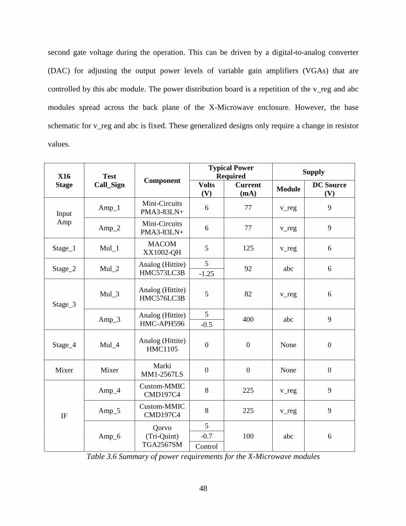
48
second gate voltage during the operation. This can be driven by a digital-to-analog converter
(DAC) for adjusting the output power levels of variable gain amplifiers (VGAs) that are
controlled by this abc module. The power distribution board is a repetition of the v_reg and abc
modules spread across the back plane of the X-Microwave enclosure. However, the base
schematic for v_reg and abc is fixed. These generalized designs only require a change in resistor
values.
X16 Stage
Test Call_Sign Component
Typical Power Required Supply
Volts (V)
Current (mA) Module DC Source
(V)
Input Amp
Amp_1 Mini-Circuits PMA3-83LN+ 6 77 v_reg 9
Amp_2 Mini-Circuits PMA3-83LN+ 6 77 v_reg 9
Stage_1 Mul_1 MACOM XX1002-QH 5 125 v_reg 6
Stage_2 Mul_2 Analog (Hittite) HMC573LC3B
5 92 abc 6
-1.25
Stage_3 Mul_3 Analog (Hittite)
HMC576LC3B 5 82 v_reg 6
Amp_3 Analog (Hittite) HMC-APH596
5 400 abc 9
-0.5
Stage_4 Mul_4 Analog (Hittite) HMC1105 0 0 None 0
Mixer Mixer Marki MM1-2567LS 0 0 None 0
IF
Amp_4 Custom-MMIC CMD197C4 8 225 v_reg 9
Amp_5 Custom-MMIC CMD197C4 8 225 v_reg 9
Amp_6 Qorvo
(Tri-Quint) TGA2567SM
5 100 abc 6 -0.7
Control Table 3.6 Summary of power requirements for the X-Microwave modules

49
The v_reg modules use low-noise, fast transient response and low-dropout regulators
(Texas Instruments TPS7A4501). The primary reason for this choice is its capability of
producing all the desired voltages with small adjustment in resistor values. The schematic
includes decoupling capacitors and adjustment resistors with the IC as shown in Figure 3.18.
Figure 3.18 Altium schematic for the v_reg module based on the TPS7A4501
The circuit net identified V_IN is connected to the DC SynQor source and V_OUT is
connected to the desired component. C1 and C2 are both X7R dielectric 10 μF capacitors placed
at the input and output of the regulator IC. The regulator is always in enabled condition (EN tied
high). The resistors, R1 and R2, set the output voltage, V_OUT, while maintaining V_Adj of
1.21 Volts and I_Adj of 3 μA. The equation for the output voltage is given in Equation 3.1.
VOUT = VADJ ∗ �1 + R1R2� + 𝐼𝐼𝐴𝐴𝐴𝐴𝐴𝐴 ∗ 𝑅𝑅1 (Equation 3.1)

50
Figure 3.19 Altium 2D and 3D layout for v_reg module
The 2D and 3D views from Altium are given in Figure 3.19. The module (dimensions
535 mil x 670 mil) is fabricated on 60-mil thick FR-4 and has mounting holes compatible with
the grid of X-Microwave modules. The regulator IC has a SOT-223 package with low density
footprint while the footprints for capacitors and resistors are 1206 and 0805, respectively.
Figure 3.20 Offset Compensation for LDO Resistor calculation

51
Since there are many possible combinations for values of R1 and R2, a MATLAB code
(APPENDIX: ldo_calc_local.m) is used to give the best fit. The R2 should not exceed R2_max,
4.17 KΩ, to reduce errors in output caused by Adjust pin bias current, I_Adj. All the available
resistor values less than R2_max are used in the code for calculation. If the measured voltage is
off from expected, the visual peaks in figure generated will provide the next better values for
both the resistors. The peaks are selected and the co-ordinates for offset compensation are
entered in the code to obtain the plot shown in the Figure 3.20.
X16 Stage
Test Call_Sign Component Required (V) Expected
(V)
Resistors (Ohm)
Supply DC Source
(V) Final v_reg R1 R2
Input Amp
Amp_1 Mini-Circuits PMA3-83LN+ 6 6 6.080 3650 909 9
Amp_2 Mini-Circuits PMA3-83LN+ 6 6 6.080 3650 909 9
Stage_1 Mul_1 MACOM XX1002-QH 5 5 5.051 1620 511 6
Stage_2 Mul_2 Analog (Hittite)
HMC573LC3B 5 5.26
abc 5.310 1070 316 6
Stage_3
Mul_3 Analog (Hittite)
HMC576LC3B 5 5 5.051 1620 511 6
Amp_3 Analog (Hittite)
HMC-APH596 5 6.12
abc 6.178 1690 412 9
IF
Amp_4 Custom-MMIC CMD197C4 8 8 8.003 5600 1000 9
Amp_5 Custom-MMIC CMD197C4 8 8 8.003 5600 1000 9
Amp_6 Qorvo
(Tri-Quint) TGA2567SM
5 5.28 abc 5.310 1070 316 6
Table 3.7 Resistor values for v_reg modules
The values of the resistors used in the current version are summarized in the Table 3.7.
The abc modules also have a regulator IC on them in addition to the main controller. The

52
requirement and calculation for different voltage outputs other than 5V, 6V or 8V on the abc
modules is explained through Table 3.8 and Table 3.9.
The abc modules use an IC from Hittite (now Analog Devices, HMC980LP4E SMT) to
automatically sequence the power for active components that need gate voltage to adjust for
certain drain current. This IC is chosen as it can support the currents and required voltages for
current application. Additionally, it has the second gate voltage output that can be used to control
the output power of the active components.
While most of the functional description is provided in the datasheet, important features
and practical considerations are noted here. This IC takes two external voltages: the supply
voltage (VDD) and digital voltage (VDIG). On the abc module, these are derived from the DC
power supply by using two linear voltage regulators. VDD is taken from the v_reg circuit on abc
module. VDIG is taken from Texas Instruments (uA78M33) positive voltage regulator that
outputs a fixed voltage of 3.3 Volts. The current design uses two separate inputs on abc module
which can be reduced to one with another set of regulator ICs. A few test modules did not work
if VDIG is turned on after VDD.
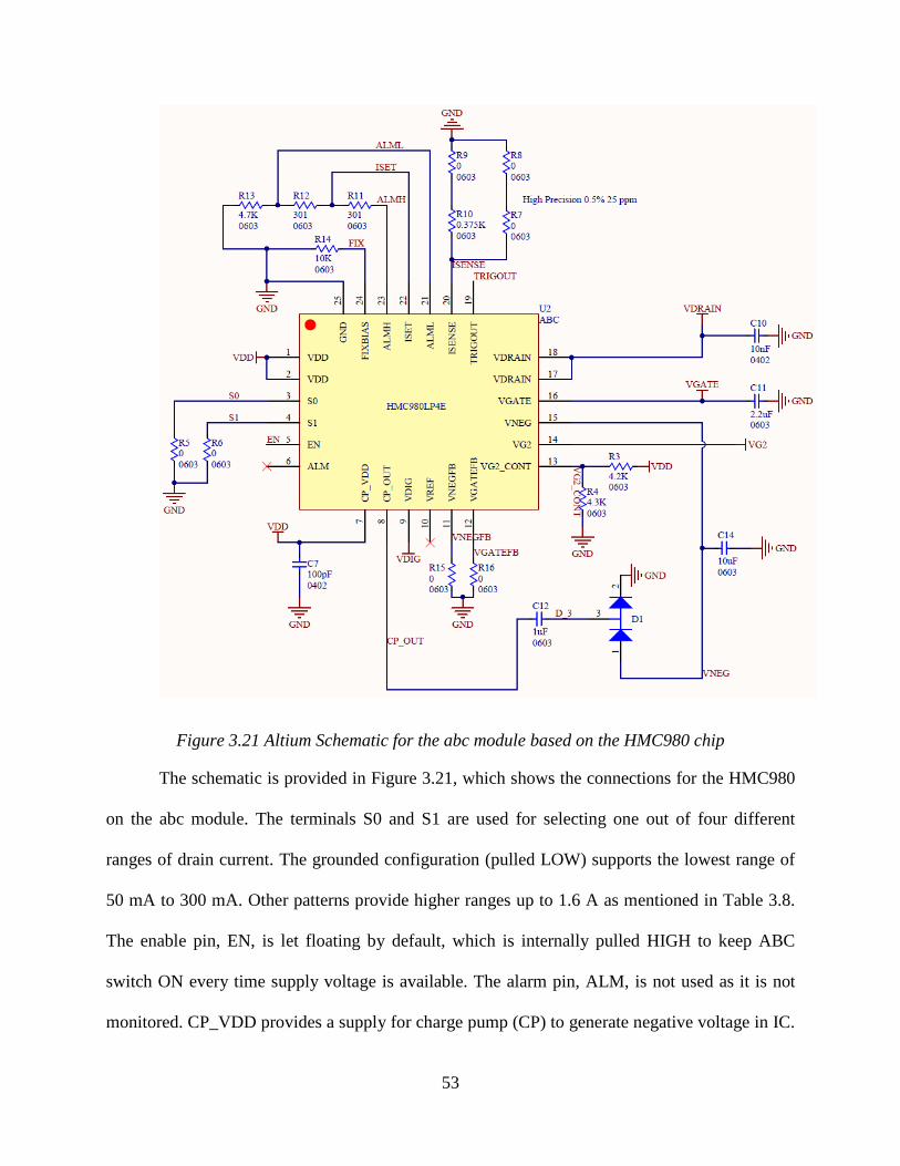
53
Figure 3.21 Altium Schematic for the abc module based on the HMC980 chip
The schematic is provided in Figure 3.21, which shows the connections for the HMC980
on the abc module. The terminals S0 and S1 are used for selecting one out of four different
ranges of drain current. The grounded configuration (pulled LOW) supports the lowest range of
50 mA to 300 mA. Other patterns provide higher ranges up to 1.6 A as mentioned in Table 3.8.
The enable pin, EN, is let floating by default, which is internally pulled HIGH to keep ABC
switch ON every time supply voltage is available. The alarm pin, ALM, is not used as it is not
monitored. CP_VDD provides a supply for charge pump (CP) to generate negative voltage in IC.

54
CP_OUT when connected to VNEG pin generates the least negative voltage of -2.46 Volts at
VNEG pin. A dual series schottky barrier diode (ON SemiconductorBAT54SL) is used in series
with the capacitor between these pins. VNEGFB and VGATEFB are not populated, as they are
not used in Master configuration. A second voltage control, VG2_CONT, generates the VG2 for
second gate. VG2 is 1.3 Volts less than the VG2_CONT as in Equation 3.2.
𝑉𝑉𝐺𝐺2 = 𝑉𝑉𝑉𝑉𝑉𝑉 ∗ 𝑅𝑅4(𝑅𝑅3+𝑅𝑅4)
− 1.3 𝑉𝑉𝑉𝑉𝑉𝑉𝑉𝑉 (Equation 3.2)
However, there is another OP-Amp section that can drive this VG2_CONT without R3
and R4 for more control over VG2. VDRAIN and VGATE are the nets to be connected to the
slave device, such as an amplifier or frequency multiplier. TRIGOUT generates the VDIG,
typically +3.3 V, when abc module is working properly. The ISENSE pin has the resistor
denoted RSENSE tied to ground, which controls the drain current by the formula given in
Equation 3.3.
𝐼𝐼𝑉𝑉𝑅𝑅𝐼𝐼𝐼𝐼𝐼𝐼 = 150𝑅𝑅𝑅𝑅𝑅𝑅𝑅𝑅𝑅𝑅𝑅𝑅
𝐼𝐼𝐴𝐴𝐴𝐴𝐴𝐴𝐴𝐴𝐴𝐴𝐴𝐴 (Equation 3.3)
RSENSE is a parallel combination of two resistors in series. These can be populated to
achieve a more accurate value of IDRAIN. Of the remaining the nets are for maintaining fixed
bias, currents and alarm signals. ALML, ISET, ALMH and FIXBIAS are connected via high-
accuracy resistors, as mentioned in the datasheet. Finally, the supply voltage is dependent on the
VDRAIN, IDRAIN and the internal resistance of the switch is obtained as per Equation 3.4.
RDS_ON is dependent on the condition set by S0 and S1, as indicated in Table 3.8 depending on
the IDRAIN requirement.
𝑉𝑉𝑉𝑉𝑉𝑉 = 𝑉𝑉𝑉𝑉𝑅𝑅𝐼𝐼𝐼𝐼𝐼𝐼 + 𝐼𝐼𝑉𝑉𝑅𝑅𝐼𝐼𝐼𝐼𝐼𝐼 ∗ 𝑅𝑅𝑉𝑉𝑅𝑅_𝑂𝑂𝐼𝐼 (Equation 3.4)

55
S1 S0 RDS_ON (Ω) IDRAIN (A)
GND (0) GND (0) 2.8 0.05 – 0.3
GND (0) VDIG (1) 1.55 0.3 – 0.6
VDIG (1) GND (0) 0.85 0.6 – 1.2
VDIG (1) VDIG (1) 0.7 1.2 – 1.6
Table 3.8 Summary of different drain current configurations for the abc module
Based on the values provided in Table 3.8 for the drain current configuration that shows
the RDS-ON values, we can calculate the VDD required for abc modules from Equation 3.4. A
total of three abc modules are needed in this implementation. Table 3.9 shows the drain current
requirements and voltages that provide the VDD necessary for the controller IC. RSENSE is also
given for the corresponding IDRAIN.
X16 Stage
Test Call_Sign Component VDRAIN
(V) IDRAIN
(mA) RDS_ON
(Ω) VDD (V)
RSENSE (Ω)
Stage_2 Mul_2 Analog (Hittite) HMC573LC3B 5 92 2.8 5.26 1630
Stage_3 Amp_3 Analog (Hittite) HMC-APH596 5 400 2.8 6.12 375
IF Amp_6 Qorvo
(Tri-Quint) TGA2567SM
5 100 2.8 5.28 1500
Table 3.9 Calculation of VDD for abc modules
The IC on the abc modules has protective features against faults and sequences the power
on and off to ensure the safety of the slave device. The latest configuration supports the master
mode (only one abc module per amplifier or multiplier) for depletion mode transistors. Previous
configurations tested in the laboratory supported only enhancement mode devices which are not

56
used in the GHSR design. This is the revised version, which in general can also support both
modes just by floating or grounding the VNEGFB and VGATEFB as mentioned in the datasheet.
Extra circuitry can be left unpopulated for the supported modes. TRIG output has a pad to
monitor +3.3 volts and the ENABLE pad is provided to support remote control. This abc module
is designed to function as an evaluation board that should support every mode and control all
devices in the supported range. However, a subsequent version has bias and feedback resistors
for VGATE to adjust the lowest voltage that VG1 reaches before bias. This is for safe operation
of the components that have restrictions on absolute maximum rating for the lowest gate voltage.
Figure 3.22 Altium schematic of the Op-Amp circuit in the abc modules
The Op-Amp circuitry presented in Figure 3.22 can take the voltages from the VDD to
function as a single supply-inverting amplifier. Components can be simply understood from the
design and redundant parts are added for future control and filtering if necessary. This Op-Amp

57
is a Texas Instruments (OPA847) IC with ultra-low noise and high gain bandwidth of 3.9 GHz.
The input is fed by an SMP connector same as the Stage_0 for inputs. The values are to be
chosen carefully for proper oscillations at the output at the desired frequencies. ADS models
available online were used to determine the swing from the lowest to highest required voltage for
VG2_CONT.
The layouts for the abc board can be seen in Figure 3.23 and Figure 3.24. These are also
fabricated on 60-mil thick FR-4 substrate. The Op-Amp support circuitry can be seen on the
bottom-right with the flushed cutout for an SMP connector.
Figure 3.23 Altium 2D layout of abc module
U1 is the same SOT223-6 v_reg IC and U3 is the SOT223-4 regulator for VDIG. U2 is
the active bias controller (HMC980LP4ETR) with 24 pins QFN package with a thermal pad and
medium density. D1 is the schottky diode with SOT23 package. OP-Amp is also SOT23-6 lead
package with medium density. ENABLE and TRIGGER pads for test and control can be seen in

58
3D layouts. The 3D bottom view shows the exposed ground for heat conduction in the modules
that might have high current requirement. More ground via are added for return paths and proper
heat sinking.
Figure 3.24 Altium 3D layout of abc module – Top (left) and Bottom (right) View
3.6 INTEGRATION
The frequency multiplier is enclosed in separate aluminum cases. Stage_0 shown in its
implementation has an enclosure with a “bullet” connector feeding the X-Microwave enclosure.
The 2.4 GHz PLO is a frequency synthesizer inside a separate box near Stage_0. The modules on
the top grid are arranged as a chain and connected by the jumpers. The integration plan is shown
in Figure 3.25.
The input to the enclosure is on the bottom left corner and done through a SMP plug and
the PLO signal through the top feeding the 38 GHz filter. The output uses a pin and Super SMA
connector from Southwest Microwave. The power required for the modules comes from the back
plane of the grid. As mentioned in Section 3.5, the power distribution modules are designed to fit
in the X-Microwave format. The enclosure gets the power from feed through terminals to filter

59
any possible interference. The integration plan provides the legend for different blocks and
modules.
Figure 3.25 Integration layout in X-Microwave format (similar to ref [39])

60
3.7 MEASURED RESULTS
We performed measurements to characterize the performance of individual stages. First,
the modules are characterized and scattering parameter responses are compared with reference
data for each stage. This reference data is taken from IC/die manufacturer and co-simulated in
ADS to include the effects of the input and output attenuators. The measured data includes the
responses taken from CReSIS labs and measured data files made available by the courtesy of X-
Microwave [27].
3.7.1 AMPLIFIERS
The plots of S-parameter responses for different amplifier modules in X-Microwave
format are provided in this section. Figure X and X show the insertion gain (S21) and input
return loss (S11) as a function of frequency for the amplifiers listed in Table 3.5. The desired
band of operation is marked with vertical green colored lines.

61
Figure 3.26 Measured and expected Gain and Return loss of 2.5 – 3.5 GHz Amplifier module: Amp-1
Figure 3.26 shows the comparison of responses for Amp-1 multi-chip module (3dB_in –
PMA3-83LN+ – 3dB_out) that should provide a gain of 15.5 dB in the desired 2.5 – 3.5 GHz
band as per specifications. The measurements are in good agreement and return loss of 20 dB.
1 1.5 2 2.5 3 3.5 4 4.5 5 5.5 6
Frequency in GHz
12
13
14
15
16
17
18
Mag
nitu
de (d
B)
S2 1
CReSIS
S2 1
Reference
S2 1
X-UW
Amp-1 S-Parameters
1 1.5 2 2.5 3 3.5 4 4.5 5 5.5 6
Frequency in GHz
-35
-30
-25
-20
-15
-10
Mag
nitu
de (d
B)
S1 1
CReSIS
S1 1
Reference
S1 1
X-UW

62
Figure 3.27 Measured and expected Gain and Return loss of 2.5 – 3.5 GHz Amplifier module: Amp-2
Figure 3.27 depicts the responses for Amp-2 module (PMA3-83LN+) to provide a 21.5
dB gain for the 2.5 – 3.5 GHz band to drive the Stage-1 x2multiplier. The measurements are in
good agreement and a decent good return loss around 12 dB.
1 1.5 2 2.5 3 3.5 4 4.5 5 5.5 6
Frequency in GHz
12
14
16
18
20
22
24
26
28M
agni
tude
(dB
)S
2 1CReSIS
S2 1
Reference
S2 1
X-UW
Amp-2 S-Parameters
1 1.5 2 2.5 3 3.5 4 4.5 5 5.5 6
Frequency in GHz
-35
-30
-25
-20
-15
-10
-5
0
Mag
nitu
de (d
B)
S1 1
CReSIS
S1 1
Reference
S1 1
X-UW

63
Figure 3.28 Measured and expected Gain and Return loss of 2 – 18 GHz Amplifier module: Amp-4 & Amp-5
0 2 4 6 8 10 12 14 16 18 20
Frequency in GHz
0
2
4
6
8
10
12
Mag
nitu
de (d
B)
S2 1
CReSIS
S2 1
Reference
S2 1
X-UW
Amp-4 S-Parameters
0 2 4 6 8 10 12 14 16 18 20
Frequency in GHz
-50
-40
-30
-20
-10
0
Mag
nitu
de (d
B)
S1 1
CReSIS
S1 1
Reference
S1 1
X-UW

64
Figure 3.28 shows the comparison of responses for 2 – 18 GHz Amp-4 multi-chip
module (3dB_in – CMD197C4 – 3dB_out). The roll off is expected as seen from the reference
response. There is a good match between the results.
The reference response can be more accurate if we have the original layout for EM
response. However, the circuit in ADS uses CPWG with different lengths to model the signal
traces between components. The circuit is shown in Figure 3.29. The measurements are in good
agreement with X-Microwave results and return loss around 15 dB. Amp-4 and Amp-5 are
identical modules cascaded to provide more gain. Therefore, the responses were not included.
Figure 3.29 Co-simulated ADS circuit for the 2 – 18 GHz Amplifier module: Amp-4 & Amp-5

65
Figure 3.30 Measured and expected Gain and Return loss of 2 – 18 GHz Amplifier module: Amp-6
Figure 3.30 depicts the responses for Amp-6 module (TGA2567SM) to provide a 17 dB
gain for the 2 – 18 GHz chirp. The gain of this amplifier can be controlled by varying the second
gate voltage (+1.44 V for the displayed response). From the responses for gain and return loss,
there is a good similarity in the ripple and nulls respectively.
0 2 4 6 8 10 12 14 16 18 20
Frequency in GHz
12
14
16
18
20
22M
agni
tude
(dB
)
S2 1
CReSIS
S2 1
Reference
Amp-6 S-Parameters
0 2 4 6 8 10 12 14 16 18 20
Frequency in GHz
-50
-40
-30
-20
-10
0
Mag
nitu
de (d
B)
S1 1
CReSIS
S1 1
Reference

66
3.7.2 FREQUENCY MULTIPLIERS
The characterization of the frequency multiplier modules includes measurements of the
return losses at both ports, suppression of harmonics and conversion gain/loss. The plots of
return losses for the Stage-1 x2 multiplier (3dB_in – XX1002-QH – 5dB_out), Mul-1,
upconverting the 2.5 – 3.5 GHz to 5 – 7 GHz is shown in Figure 3.31. In the desired bands,
between vertical green lines, there is good match between measured and reference data. The
return losses are closer to 20 dB at input and output.
Figure 3.31 Measured and expected Input and Output Return loss of 2.5 – 3.5 GHz to 5 – 7 GHz Multiplier: Mul-1
2 4 6 8 10 12 14
Frequency in GHz
-60
-50
-40
-30
-20
-10
0
Mag
nitu
de (d
B)
Mul-1 Input S-Parameters
S1 1
CReSIS
S1 1
Reference
4 6 8 10 12 14 16 18 20
Frequency in GHz
-60
-50
-40
-30
-20
-10
0
Mag
nitu
de (d
B)
Mul-1 Output S-Parameters
S2 2
CReSIS
S2 2
Reference

67
Figure 3.32 shows the conversion gain and output characteristics of Mul-1. The first
subplot compares the output power over wide frequency range with the synthesized sweep of 2.5
– 3.5 GHz at input. The desired output power in 5 – 7 GHz band is around 10 dB closer to the
specified datasheet values in parenthesis. The fundamental, third and fourth harmonics are
plotted and have good suppression values as desired.
Figure 3.32 Measured and expected Output and Leakage power of 2.5 – 3.5 GHz to 5 – 7 GHz Multiplier: Mul-1
2 4 6 8 10 12 14
Frequency in GHz
-50
-40
-30
-20
-10
0
10
20
Out
put P
ower
, dB
m
CReSIS
X-UW
Multiplied 2.5-3.5 GHz sweep
4.5 5 5.5 6 6.5 7 7.5
Frequency in GHz
-50
-40
-30
-20
-10
0
10
20
Pow
er, d
Bm
10 dBm (11)
Output 5-7 GHz
2 2.5 3 3.5 4
Frequency in GHz
-50
-40
-30
-20
-10
0
Leak
age,
dB
m
-32 dBc (-35)
Fundamental
7 7.5 8 8.5 9 9.5 10 10.5 11
Frequency in GHz
-50
-40
-30
-20
-10
0
Leak
age,
dB
m
-30 dBc (-30)
Third Harmonic
Mul-1 Characteristics
10 11 12 13 14
Frequency in GHz
-50
-40
-30
-20
-10
0Le
akag
e, d
Bm
-18 dBc (-20)
Fourth Harmonic

68
The plots of return losses for the Stage-2 x2 multiplier (5dB_in – HMC573LC3B –
3dB_out), Mul-2, are shown in Figure 3.33. This multiplies the 5 – 7 GHz chirp to output 10 –
14 GHz. The return losses measured are compared with the reference data to see a perfect match
in the response.
Figure 3.33 Measured and expected Input and Output Return loss of 5 – 7 GHz to 10 – 14 GHz Multiplier: Mul-2
2 4 6 8 10 12 14
Frequency in GHz
-60
-50
-40
-30
-20
-10
0
Mag
nitu
de (d
B)
Mul-2 Input S-Parameters
S1 1
CReSIS
S1 1
Reference
4 6 8 10 12 14 16 18 20
Frequency in GHz
-60
-50
-40
-30
-20
-10
0
Mag
nitu
de (d
B)
Mul-2 Output S-Parameters
S2 2
CReSIS
S2 2
Reference

69
Figure 3.34 shows a comparison of output powers for a full band input and synthesized
sweep of 5 – 7 GHz. The extra loss can be attributed to the effect of extra attenuation and input
drive levels for multiplier. However, the roll off is expected in the desired 10 – 14 GHz band at
output. There is a good agreement between measured suppression and the specified values. The
discontinuities in the response is an artifact of the analyzer used for measurement.
Figure 3.34 Measured and expected Output and Leakage power of 5 – 7 GHz to 10 – 14 GHz Multiplier: Mul-2
5 10 15 20 25 30 35
Frequency in GHz
-50
-40
-30
-20
-10
0
10
20
Out
put P
ower
, dB
m
X-UW
Multiplied 5-7 GHz sweep
9 10 11 12 13 14 15
Frequency in GHz
-50
-40
-30
-20
-10
0
10
20
Pow
er, d
Bm
4 dBm
Output 10-14 GHz
4 4.5 5 5.5 6 6.5 7 7.5 8
Frequency in GHz
-50
-40
-30
-20
-10
0
Leak
age,
dB
m
-19 dBc (-20)
Fundamental
14 15 16 17 18 19 20 21 22
Frequency in GHz
-50
-40
-30
-20
-10
0
Leak
age,
dB
m
-27 dBc (-25)
Third Harmonic
Mul-2 Characteristics
20 22 24 26 28
Frequency in GHz
-50
-40
-30
-20
-10
0Le
akag
e, d
Bm
-18 dBc (-15)
Fourth Harmonic

70
The measurement for the Stage-3 x2 multiplier (3dB_in – HMC576LC3B – 3dB_out),
Mul-3, is shown in Figure 3.35. The output power is around 14 dB (17 dB – 3 dB) as expected in
desired band.
Figure 3.35 Measured Output power of 10 – 14 GHz to 20 – 28 GHz Multiplier: Mul-3
Mul-3 Characteristics
16 18 20 22 24 26 28 30
Frequency in GHz
5
10
15
20
Out
put P
ower
, dB
m
X-UW

71
3.7.3 DOWN-CONVERSION MIXER
The mixer module (3dB_RF – MM1-2567 – 3dB_IF) response is shown in Figure 3.36.
The scattering parameters are plotted as a function of frequency 40 – 56 GHz at RF port. The
module has a 15 dB conversion loss as expected (3dB + 9 dB + 3dB). The return loss at RF port
is good and close to 15 dB.
Figure 3.36 Measured Conversion and return losses of 40 – 56 GHz to 2 – 18 GHz down-converting Mixer
40 42 44 46 48 50 52 54 56
Frequency in GHz
-50
-45
-40
-35
-30
-25
-20
-15
-10
-5
0
Mag
nitu
de (d
B)
Mixer S-Parameters
Conversion Loss
RF Reflection
IF Reflection

72
3.7.4 STAGE_0
The completely assembled Stage_0 board is shown in Figure 3.37.
Figure 3.37 Photograph of the assembled Stage_0 board used for characterization
Two similar boards with serial number 1 and 2 were populated to check for the response.
Figure 3.38 provides a comparison of conversion loss for two separate boards. Clearly, there is a
close agreement between the boards except for additional loss on sn_1. The first Stage_0 board
sn_1 was run through the reflow machine more than 5 times to set the heat profile and stepped
assembly of components. However, sn_2 is reflowed only once. The nominal input power for RF
is -2 dBm and 16 dBm for LO to output -33.5 dBm chirp to x16 frequency multiplier. The return
losses at the input are very good, as high as 20 dB. The output return loss is around 10 dB as
seen in Figure 3.39.

73
Figure 3.38 Measured Conversion loss for Stage_0 upconverter boards
Figure 3.39 Input and Output Return losses of two Stage_0 boards
2.5 2.6 2.7 2.8 2.9 3 3.1 3.2 3.3 3.4 3.5
Frequency, GHz
-50
-45
-40
-35
-30
-25
-20
-15
-10
-5
0
Mag
nitu
de, d
B
Stage_0 sn_1 vs sn_2 Up-conversion
Expected 31.5 dB CL
sn_1
sn_2
0.1 0.2 0.3 0.4 0.5 0.6 0.7 0.8 0.9 1 1.1
Frequency, GHz
-50
-40
-30
-20
-10
0
Mag
nitu
de, d
B
Stage_0 sn_1 vs sn_2 Input Return Losses
sn_1
sn_2
2.5 2.6 2.7 2.8 2.9 3 3.1 3.2 3.3 3.4 3.5
Frequency, GHz
-50
-40
-30
-20
-10
0
Mag
nitu
de, d
B
Stage_0 sn_1 vs sn_2 Output Return Losses
sn_1
sn_2

74
CHAPTER 4 FILTER DESIGN
4.1 DESCRIPTION OF FILTER STRUCTURES IN THE X16
FREQUENCY MULTIPLIER
This section describes the procedure of selection and design of the filters employed
throughout the design. A few of them were pre-designed and available in market, while most
others were designed and fabricated in house, for the sole purpose of this project. Table 4.1 gives
a summary of all the filters and their technologies. Highlighted ones are discussed in this chapter.
Stage Type Frequency
(GHz) Technology Description
Manufacturer
/Designer
Stage_0
BPF 0.1 - 1.1 Lumped elements CReSIS
BPF 2.2 - 2.6 Lumped elements Mini-Circuits
BPF 2.5 - 3.5 Lumped elements Lark Engg.
Stage_1 BPF 5 - 7 Distributed
interdigital cavity CReSIS
Stage_2 BPF 10 - 14 Distributed
interdigital cavity CReSIS
Stage_3 BPF 20 - 28 Distributed
edge-coupled microstrip
CReSIS
Ultrasource
Stage_4 BPF 40 - 56 Distributed
edge-coupled microstrip
CReSIS
Ultrasource
LO BPF 38 Distributed
edge-coupled microstrip
CReSIS
Ultrasource
IF
LPF 18 Distributed
Stripline
CReSIS
Hughes
HPF 2 Distributed
Stripline
CReSIS
Hughes
Table 4.1 Summary of Filters used in the X16 Frequency Multiplier

75
Stage_3, Stage_4 and LO band-pass filters are designed and validated in Advanced
Design System (ADS). Stage_1 and Stage_2 filters are simulated in Ansys High Frequency
Structure Simulator (HFSS) to validate the original design from Mician μWave Wizard. Stage_0
filter for 0.1 – 1.1 GHz is co-simulated in ADS by importing Gerber files from Altium Designer
and design values from Genesys. The following subsections show the detailed design and
validation of the highlighted filters developed for the thesis.
4.2 LUMPED LC FILTER
4.2.1 0.1 – 1.1 GHz BANDPASS FILTER
A lumped-element filter using capacitors and inductors is optimized in ADS with
imported Gerber files from Altium Designer. The filter is a series of low-pass and high-pass
sections. Low-pass section is a 7th order minimum capacitance filter and high-pass section is a
7th order minimum inductance filter. The base design layout in Altium Designer from which the
optimization is later performed is presented below for reference in Figure 4.1. The ports on the
corners have 9 via (3x3) to the bottom pad that lands on the PCB.
Figure 4.1 Altium 3D layout of Lumped LC 0.1 - 1.1 GHz BPF Top and Bottom views

76
The Gerber files of top and plated vias are imported to ADS EM layout. The layers are
associated with the 30-mil Rogers 4350 substrate saved as symbol for future use at other
frequencies. This is used for a circuit/EM co-simulation, using s-parameters for the inductors and
assuming ideal capacitors. A view of the circuit/EM co-simulation setup is shown in Figure 4.2.
The input port is located on the right hand side in all the layouts.
Figure 4.2 ADS schematic of Lumped LC 0.1 - 1.1 GHz BPF
Figure 4.3 Photograph of the assembled 0.1 – 1.1 GHz bandpass filter on Stage_0 board
The filter is oriented in this way to land on the Stage_0 board as shown in Figure 4.3.
Similar footprint is used for PCB layout of 2.5 – 3.5 GHz filter from Lark Engineering. The
layout can be used for other frequency ranges with optimized values for resonating elements.

77
This gives flexibility of design with a fixed layout and simulation setup for evaluation. However,
the only limitation is the LC filters because of the performance at higher frequencies and
tolerances will result in deviation from expected response. The plot of simulated and measured
responses is provided in the Figure 4.4. The slight offset in the band for few MHz is expected
because the qualify factor of the capacitors decreases as a function of frequency. However, the
initial design for extra bandwidth proves essential in this scenario to compensate for the shift in
pass band. The measured return loss is better than expected around 15 dB.
Figure 4.4 Co-simulated and Measured Responses from Lumped LC 0.1 - 1.1 GHz BPF

78
4.3 INTERDIGITAL CAVITY FILTERS
4.3.1 MOTIVATION
Interdigital cavity filters are widely seen in the commercial designs. A study of the
literature [40] similar to the parallel-coupled resonators in alumina band-pass filters prove that
this is another viable option for fabrication. The resonators are quarter wavelength long and are
shorted at one end alternatively. Unlike the alumina edge-coupled lines, the interdigital filter has
only one open end on resonators. Coupling is because of the fields fringing between the
resonator elements. Here, the medium is air and the enclosed cavity along with resonators are
made of aluminum.
The interdigital filters from the reference [40] for wide band are analytically implemented
to verify the feasible fabrication at CReSIS. While the values turned out to be realizable, further
development was done to replicate the design values for the Stage_1 and Stage_2 filters. The
desired frequency bands are 5 – 7 GHz and 10 – 14 GHz, respectively. It was observed that the
values from the theoretical calculations in one-pass could not completely realize the filter. Some
compensation is necessary by taking feedback from the shifts or anomalies in the response. The
generalized code in MATLAB based on design equations successfully generates the values that
are close but not exactly a single-pass best design. CAD tools were used to perform synthesis as
well as optimization. In particular Mician μWave Wizard [41] is a highly reliable tool for this
technology.
Mician μWave Wizard is capable of simulation and design of wide range of passive
waveguide components including filters accurately and faster sweep response. The product page
[41] describes this is possible by using the method of Mode Matching (MM) and its derivatives.

79
While a 3D FEM simulator is available in the tool, processing speed is improved by the 2D FEM
and boundary contouring. Evaluation licenses were kindly provided by Mician. The component
to be simulated is considered as several building blocks (available in the library) such as
waveguides, discontinuities, and any other feature specific to the model. Eventually, S-
parameters for each block are calculated and simulates full 3D model by multi-modal element
connections.
The optimization in μWave Wizard can be performed in the control window for specific
variables or parameters. In our case, the input port feed pin diameter is fixed and the gaps inside
the cavity are limited by the tools available in fabrication facility. The simulated values for
design are checked to see if the model can be made in-house before further optimization or
validation in HFSS. A few of the filter designs have several versions that offer strict roll-off with
higher order while lower-order designs were used for test purposes.
The measured responses for several other filters validated in HFSS and fabricated in-
house added up to choose this CAD tool for Interdigital Cavity filter design. The process of
simulated response in μWave Wizard is followed by a validation check in HFSS and turned into
computer aided manufacturing facilities. All synthesized designs were verified to have a good
agreement between measured and simulated performance.
4.3.2 5 – 7 GHz BANDPASS FILTER
The 3D model from HFSS EM simulation is shown in Figure 4.5. The top-view of the
filter model for complete visibility of interdigital rods is shown below in Figure 4.6. The filter is
a 11-section design for steep roll-off in 5 – 7 GHz band. Interdigital elements can be either
cylindrical or cuboidal. For ease of fabrication, the current design employs cuboidal rods with

80
square cross-section. The cross sectional width and length of interdigital rods accompanied by
the gaps between rods and the open sections act as inductance and capacitance respectively. The
theoretical design formulae show the clear calculation of even and odd mode capacitances for
calculating dimensions [40].
Figure 4.5 3D View of HFSS model for Interdigital Cavity 5 - 7 GHz BPF
The resonators colored in red and the cavity around them is aluminum. Hermetically
sealed pins from Southwest Microwave, 290-06G, are used for the ports. The cylindrical shape
on outer side, colored in pink, has dielectric medium assigned as Arlon AD410 with a relative
permittivity of 4.1. The inner co-axial cylinder is adjusted for 50-Ohm impedance with air
dielectric. This is to replicate the hermetically sealed pins in simulation. The thickness of the
filter, except on port faces, is varied to fit the enclosed cavity on the grid for launching in a
format compatible with the X-microwave modules. The model is simulated for terminal driven
solution with lumped port excitations on both the walls with ports.

81
Figure 4.6 Top and Side Views of HFSS model for Interdigital Cavity 5 - 7 GHz BPF
Relevant dimensions, in mils, for above design are presented in Table 4.2. The resonator
numbering starts from left to right in the top view. Length of interdigital rod is measured along
the Y-axis seen in the top view. Cross-section is measured in the X-Z plane seen in the side view.
The open circuit gap is measured along Y-axis seen in the top view. Note that the sum of the
length and open circuit gap gives the inner width of filter cavity, measured in the Y-axis, as
491.78 mil. Instead of accurate values up to 12 decimal places from the HFSS, model dimensions
are rounded to two places. However, at these frequencies, this round off is expected not to alter
much the response of filter redesigned from values documented in Table 4.2 and Table 4.3.
Proper rules for accurate dimensions should be followed if using a general parametrized model.
If not, problems with geometrical discontinuities and overlapping were noted in early test
designs.

82
Resonator Label
Resonator Cross-section
Resonator Length
Open-circuit Gap with wall
Filter Width (Check_Sum)
1 50x50 481.92 09.86 491.78 2 50x50 422.17 69.61 491.78 3 50x50 412.83 78.96 491.78 4 50x50 411.21 80.57 491.78 5 50x50 410.43 81.35 491.78 6 50x50 409.86 81.92 491.78 7 50x50 410.43 81.35 491.78 8 50x50 411.21 80.57 491.78 9 50x50 412.83 78.96 491.78 10 50x50 422.17 69.61 491.78 11 50x50 481.92 09.86 491.78 Table 4.2 Resonator Dimensions of HFSS model for Interdigital Cavity 5 - 7 GHz BPF
Coupling gap between rods is measured along the Z-axis seen in top or side views from
edge-to-edge of each resonator element. Note that the sum of all coupling gaps and cross section
length of 11 resonators (50 mil multiplied 11 times) gives 2588.47 mil, which is the inner length
of the filter cavity. The height, measured along the X-axis is 500 mil inside the cavity.
Figure 4.7 Photograph of a section of milled 5 – 7 GHz bandpass filter
Values for the coupling gaps between elements are provided in Table 4.3. The distance
from the wall to the first post is essential for port matching at the input and output that can be
seen in Figure 4.7. All the dimensions for the gaps are in mils.

83
Interdigital
Resonator Pair
Coupling Gap
between adjacent rods
Side_wall-1 064.01
1-2 124.68
2-3 192.82
3-4 208.53
4-5 213.49
5-6 215.70
6-7 215.70
7-8 213.49
8-9 208.53
9-10 192.82
10-11 124.68
11-Side_wall 064.01
Total Coupling Gap 2038.47
Cross-section length (11 rods) 550.00
Filter Length 2588.47
Table 4.3 Coupling Dimensions of HFSS model for Interdigital Cavity 5 - 7 GHz BPF
The similarity in EM simulation between μWave Wizard and HFSS evaluated before
fabrication is seen in Figure 4.8. The converged solution set from HFSS looks as a close fit to the
synthesized design. Good match is noticed in return loss characteristics where the null locations
closely overlapping for both responses.

84
Figure 4.8 Simulated Responses from Interdigital Cavity 5 - 7 GHz BPF
The transmission highly relies on the dimensions of internal cavity that is perfectly
fabricated in-house. Reflection, on the other hand, is dependent on proper port matching
implemented by feed through pins. The test setup has transmission lines at the input and output
of the filter ports to launch the signal from and into a planar transmission line. The pins of port
feed are landed on signal trace of module and this setup is measured as whole to characterize the
response. The effect of adding modules is co-simulated in ADS for proper comparison of the
scattering parameters. A snip of ADS schematic is presented in Figure 4.9 for reference.

85
Figure 4.9 ADS Schematic for comparison of 5 - 7GHz BPF results
A comparison of the compensated models from μWave Wizard, HFSS and measured
responses are presented in the plot in Figure 4.10. The pass band overlaps on the designed
response. The additional loss of around 0.7 dB in pass band is attributed to the loss of probes and
the feed not included in the ADS model.

86
Figure 4.10 Co-simulated and Measured Responses from Interdigital Cavity 5 - 7 GHz BPF
4.3.3 10 – 14 GHz BANDPASS FILTER
The design of Stage_2 filter for 10 – 14 GHz band is same as the Stage_1 filter for 5 – 7
GHz described in Section 4.3.2. This is also a 11th order filter with smaller dimensions because
of the higher frequencies of operation. Another working versions of this model is a 7th order
filter with slower roll off compared to current 11th order filter. The dimensions for the
interdigital resonators and related coupling gaps are presented in Table 4.4 and Table 4.5
respectively.

87
Resonator Label
Resonator Cross-section
Resonator Length
Open-circuit Gap with wall
Filter Width (Check_Sum)
1 50x50 227.86 18.04 245.89 2 50x50 195.68 50.21 245.89 3 50x50 192.27 53.62 245.89 4 50x50 192.31 53.58 245.89 5 50x50 192.42 53.47 245.89 6 50x50 192.45 53.44 245.89 7 50x50 192.42 53.47 245.89 8 50x50 192.31 53.58 245.89 9 50x50 192.27 53.62 245.89 10 50x50 195.68 50.21 245.89 11 50x50 227.86 18.04 245.89
Table 4.4 Resonator Dimensions of HFSS model for Interdigital Cavity 10 - 14 GHz BPF
Interdigital
Resonator Pair
Coupling Gap
between adjacent rods
Side_wall-1 13.24
1-2 55.69
2-3 96.54
3-4 105.35
4-5 107.56
5-6 108.21
6-7 108.21
7-8 107.56
8-9 105.35
9-10 96.54
10-11 55.69
11-Side_wall 13.24
Total Coupling Gap 973.19
Cross-section length (11 rods) 550.00
Filter Length 1523.19
Table 4.5 Coupling Dimensions of HFSS model for Interdigital Cavity 10 - 14 GHz BPF

88
The simulated responses obtained from both CAD tools are presented in Figure 4.11. As
expected, both the responses overlap each other to a large extent. Reflection and transmission
parameters agree with the simulated responses.
Figure 4.11 Simulated Responses from Interdigital Cavity 10 - 14 GHz BPF
After fabrication, the test setup is has the transmission lines at the input and output of
filter. A schematic circuit was generated in ADS is used to obtain touchstone model that could be
used for comparison with the measure response. The plot of the response is presented in Figure
4.12. The extra loss of around 1 dB present in this filter is attributed to the effect of probes and
feeds not included in the co-simulated reference. For this particular filter, the fabrication was
subsequently improved, which will result in improved performance.

89
Figure 4.12 Co-simulated and Measured Responses from Interdigital Cavity 10 - 14 GHz BPF

90
4.4 ALUMINA BAND PASS FILTERS
4.4.1 MOTIVATION
As the frequency of operation of filters increases, tolerances in the fabrication process
might affect the response of the filters in a more significant way. The filter for Stage – 2 using
Interdigital technique has pushed to the limits of fabrication facility at CReSIS. Various micro-
strip filters using stepped impedance and substrate-integrated-waveguide (SIW) were reviewed
and evaluated as feasible design [21]. Simultaneously, edge-coupled filters were simulated to
obtain better responses.
In this section, the design flow for three different filter designs for 20-28 GHz, 40-56
GHz and 38 GHz filter is described. The filters can be reproduced by following a similar design
flow and can be cross-verified against the dimensions. A comparison between different
responses of same filter is provided for better understanding.
Edge coupled filters printed on alumina as dielectric substrate use parallel-coupled lines
or resonators. The lines are separated by gaps that act as capacitances. Designs using ceramic
coupled line filters were reported earlier [42]. The calculation of admittances and equations or
similar design using parallel-coupled lines is provided in literature [40]. Theoretical calculations
can be performed to obtain an initial design that can be optimized. However, advanced CAD
packages ls provide powerful synthesis tools to synthesize the desired response.
In this thesis, a Chebyshev 5th order band pass filter design done in Genesys MFilter
provides the preliminary dimensions and a simulation model based on transmission lines
response. The circuit simulation is not be considered to be the final result without further

91
validation using EM simulations. Although this plan can be executed in Genesys, the preferred
option was Advanced System Design (ADS). ADS provides more flexible options for
optimization, repetition of the design cells and operations between datasets. After looking at the
evaluated results from Electro-Magnetic (EM) layout, further modifications are done as a
parametric analysis to obtain the desired response.
Figure 4.13 ADS Circuit schematic simulation setup for the Alumina BPF 20 – 28 GHz
All the filters are fifth-order edge-coupled and has six sections of parallel-coupled lines
about the length of quarter wavelength at the center frequency of operation. Figure 4.13 shows a
general layout of the 5th order or 6-section edge coupled filter. The schematic shows the co-
planar waveguide with ground (CPWG) feed at both the ports. The signal trace then encounters a
CPWG to micro-strip transition to the coupled resonators.
The design is symmetrical, that helps the optimization to run fast because of minimal set
of parametrized data. The CPWG and micro-strip line, MLIN, dimensions are fixed for each
filter. The set has nine variables related to coupled lines, CLin1 to CLin6 of micro-strip coupled
filter, denoted as MCFIL are summarized in Table 4.6 .

92
Variable Parameters Tuning or Optimizing Steps
Line Width, W w1, w2, w3 0.1 mil
Separation between Coupled lines s1, s2, s3 0.1 mil
Line Length, L l1, l2, l3 0.1 mil
Table 4.6 Parameters for Tuning and Optimization of ADS filters
The CPWG values are fixed based on the fabrication limits from UltraSource, a thin film
foundry [43]. We pushed UltraSource fabrication process to its limits and worked them to agree
on dimension values that were compatible with our designs without sacrificing performance. As
the filter is symmetric, dimensions for the coupled lines, CLin, represented as MCFIL in
schematic have similar values for the following sets: 1 and 6; 2 and 5; 3 and 4. The
corresponding EM layout is shown in Figure 4.13 for the base design of 20 – 28 GHz filter is
presented in Figure 4.14.
Figure 4.14 ADS Layout for Alumina BPF
A 0.1 mil resolution with minimum trace width or separations up to 0.5 mil minimum is
achievable on 5-mil Alumina substrate according to the discussions with UltraSource. In

93
addition, a minimum center-center distance of 13 mil between vias and not less than 10 mil from
the edge of board are specified. While one specification put restriction on CPWG feed and others
limited the pre-designed resonator section for copper traces. The current designs use 2μm thick
gold film sputtered on the top and bottom ground plane. The metallization is 500Å (±250Å) thick
TiW on both sides of the filter. All the pre-designed filter models were quickly adapted to the
change in manufacturing requirements, re-simulated and optimized based on EM simulations.
This transition caused a minor increase in loss in the pass band and higher return loss. One of the
filter is presented here for reference in Figure 4.15.
Figure 4.15 Photograph of a 20 – 28 GHz bandpass filter on Alumina

94
4.4.2 20 – 28 GHz BANDPASS FILTER
Initially, Genesys MFilter inputs are provided for a wider response in the band from 19.5
GHz to 28.5 GHz. The reason is previous experiences with similar kind of simulation followed
by verifying the milled interdigital micro-strip filter for 5 – 7 GHz. The synthesized design
values from Genesys are the inputs to parametrized model in ADS.
Consequent EM simulation can be with Momentum RF (MomRF), Momentum
Microwave (MomUW), and Finite Element Method (FEM). For the current layered filter with
few vias, MomRF simulator can estimate the S-parameter response for the micro-strip
technology layout by method of moments (MoM). This gives the results as expected as the
circuit S-parameter simulation. MomUW and FEM results are also available and close to the
MomRF but are omitted to improve visual readability from the figures.
The base design optimized for 20 – 28 GHz is fabricated with the call sign fab_01. A
comparison of the responses from the mentioned simulations are provided in Figure 4.16. The
filter has about 2 dB insertion loss and return loss greater than 12 dB everywhere in the
passband.

95
Figure 4.16 Simulated and measured response for fab_01 Alumina BPF 20 - 28 GHz
It is desired to keep the design level bandwidths longer than desired based on simulations
done to account for shifts in passband and change in bandwidth. Figure 4.16 clearly shows the
band has extended by almost 2 GHz overall and more to the right. The optimizations can only
change in steps of 0.1 mil that can alter the pass band or return loss in huge amount. This is
observed while tuning the filters before optimization. Because of the timeframe of the project
and accounting for lead times, it is better reduce risk level by fabricating more design with some
compensation. This led the designers to have more versions of the 20 – 28 GHz filters.
Two alternate versions for the base fab_01 are designed to compensate the pass band shift
in left or right direction. One version, fab_02, compensate the left shift of passband and the
other, fab_03, has much wider bandwidth to compensate both. Following Figure 4.17 shows the
individual responses of the alternative designs for 20 – 28 GHz.

96
Figure 4.17 Simulated and measured responses for fab_02 and fab_03 Alumina BPF 20 - 28 GHz
The optimization settings were individually adjusted for each design to shift the band
according to the goals set for S11 and S21 parameters. A comparison of the MomRF responses
for the three filters gives a better visualization. It is clearly seen in Figure 4.18 showing different
passbands that the simulated and measured responses for all the filters are in close agreement.
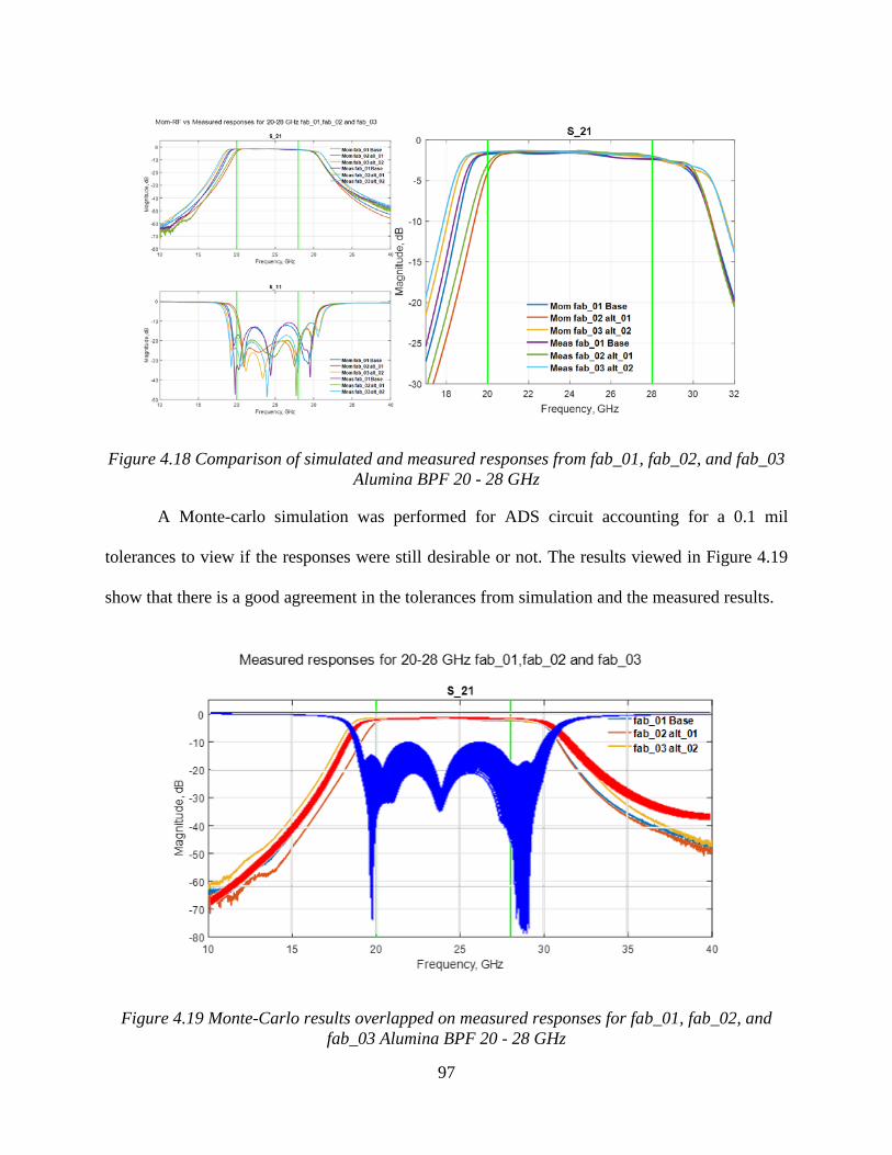
97
Figure 4.18 Comparison of simulated and measured responses from fab_01, fab_02, and fab_03 Alumina BPF 20 - 28 GHz
A Monte-carlo simulation was performed for ADS circuit accounting for a 0.1 mil
tolerances to view if the responses were still desirable or not. The results viewed in Figure 4.19
show that there is a good agreement in the tolerances from simulation and the measured results.
Figure 4.19 Monte-Carlo results overlapped on measured responses for fab_01, fab_02, and fab_03 Alumina BPF 20 - 28 GHz

98
Different sets of 20 – 28 GHz bandpass filters were sent to facilities at Michigan State
University and the National Institute for Standards and Technologies (NIST), Boulder, CO, for
measuring S-parameters using a probe station. A comparison of different measurements is
provided in Figure 4.20. The measurements from MSU are labelled – Meas and compared with
Mom-RF and schematic response. Measurements provided by courtesy of NIST are labelled
Meas2 and Meas3; both taken at 0 dBm and -10 dBm power levels. the measured responses from
two different measurement setups overlap, indicating excellent performance repeatability.. The
filters fab_01 and fab_02 also exhibited perfect match in the measurements from both facilities.
Figure 4.20 Repeatability of measurements for fab_03 Alumina BPF 20 - 28 GHz

99
The dimensions for the filters are summarized in the Table 4.7 and Table 4.8 below. The
microstrip line, MLIN, is a 50 Ohm impedance line to match the CPWG and coupled lines.
Call Sign
MCFIL_CLin_Dimensions (mil)
w1 w2 w3 s1 s2 s3 l1 l2 l3
fab_01 1.2 2.0 1.1 0.9 0.6 1.7 49.5 47.3 49.0
fab_02 1.0 2.0 2.0 0.9 1.1 1.6 50.6 46.4 47.0
fab_03 0.9 2.1 1.4 0.9 0.5 1.2 50.8 47.6 48.1 Table 4.7 Coupled lines Dimensions for fab_01, fab_02, and fab_03 Alumina BPF 20 - 28 GHz
Call Sign CPWG MLIN Total_Dim
UltraSource ADS W G L w_50 l_50 Length Width
fab_01 schem_base_FAB_Final 4.3 5.0 31.0 4.8 50.0 453.6 220.3
fab_02 schem_alt_01 4.3 5.0 31.0 4.8 50.0 450.0 222.0
fab_03 schem_alt_02 4.3 5.0 31.0 4.8 50.0 455.0 219.8
Table 4.8 CPWG, MLIN, and Total Dimensions for fab_01, fab_02, and fab_03 Alumina BPF 20 - 28 GHz
4.4.3 40 – 56 GHz BANDPASS FILTER
Similar method of optimizations repeated for 40 – 56 GHz filter resulted in fab_04. The
version to compensate slight shift in the pass band this is fab_05. However, the responses are not
satisfactory. FEM simulation to crosscheck the responses agrees with the unsatisfactory results.
While this is not a viable option for fabrication, the responses from fab_04 and fab_05 with
CPWG feed are included for reference. From the Figure 4.21, it is evident about the pass band
responses distorted at the higher end and more insertion loss. The return loss around 8 dB also
adds to these two fabs as no pass for fabrication.
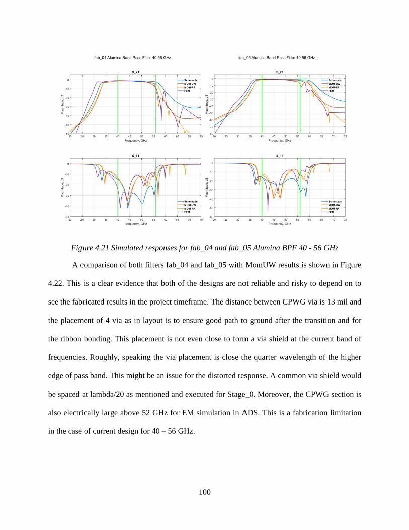
100
Figure 4.21 Simulated responses for fab_04 and fab_05 Alumina BPF 40 - 56 GHz
A comparison of both filters fab_04 and fab_05 with MomUW results is shown in Figure
4.22. This is a clear evidence that both of the designs are not reliable and risky to depend on to
see the fabricated results in the project timeframe. The distance between CPWG via is 13 mil and
the placement of 4 via as in layout is to ensure good path to ground after the transition and for
the ribbon bonding. This placement is not even close to form a via shield at the current band of
frequencies. Roughly, speaking the via placement is close the quarter wavelength of the higher
edge of pass band. This might be an issue for the distorted response. A common via shield would
be spaced at lambda/20 as mentioned and executed for Stage_0. Moreover, the CPWG section is
also electrically large above 52 GHz for EM simulation in ADS. This is a fabrication limitation
in the case of current design for 40 – 56 GHz.

101
Figure 4.22 Comparison of simulated responses from fab_04 and fab_05 Alumina BPF 40 - 56 GHz
By removing the CPWG feed was implemented to check we were able to obtain r better
responses over the complete band of interest. This reduced the filter to standard micro-strip filter.
Both filters, fab_04 and fab_05 are re-optimized for better results without the CPWG feed. The
responses were satisfactory. Either left or right shift in passband because of tolerances in

102
fabrication can be compensated by the new versions fab_06 and fab_07. This is shown in the
following Figure 4.23, where fab_06 will work for a right shift and fab_07 will work either way
conveniently because of the larger bandwidth.
Figure 4.23 Simulated responses for fab_06 and fab_07 Alumina BPF 40 - 56 GHz
The effect of removing CPWG feed clears the distorted response on the higher end.
However, the insertion loss is around 2 dB and about 0.5 dB extra at edges, this is a reliable
design better than the fab_04 and fab_05. For integration, these are ribbon bonded to the x16
frequency multiplier chain by a micro-strip to CPWG adapter, ProbePoint 0503, from J-micro
Technology [44]. Ribbon is preferred over wire at millimeter wave frequencies [45]. This 5 mil
thick adapter easily can sit beside the filter ports on same carrier board and ribbon bonded to the
CPWG trace on the module.

103
Figure 4.24 Comparison of simulated responses from fab_06 and fab_07 Alumina BPF 40 - 56 GHz
The comparison of MomUW responses for both fab_06 and fab_08 is provided in the
Figure 4.24. This figure reiterates the compensation for shift in the bands. Both of these filters
were fabricated to verify the test results. To see the improvement in the response by removing

104
the CPWG feed, a comparison between same models is provided for reference. This clearly
shows regaining the good response by switching to a pure micro-strip design. Here, Figure 4.25
shows fab_04 vs fab_06 and fab_05 vs fab_07, which are with and without CPWG feed
respectively.
Figure 4.25 Comparison of simulated responses from fab_04 and fab_06; fab_05 and fab_07Alumina BPF 40 - 56 GHz
The fabricated designs fab_06 and fab_07 were measured at University of Massachusetts,
Amherst. Figure 4.26 and Figure 4.27 show the responses compared to the circuit and EM
simulations for fab_06 and fab_07 respectively. Clearly, there is a good agreement between
Mom-UW and the measured results.

105
Figure 4.26 Simulated and measured responses from fab_06 Alumina BPF 40 – 56 GHz
Figure 4.27 Simulated and measured responses from fab_07 Alumina BPF 40 – 56 GHz
The dimensions for the fabricated designs fab_06 and fab_07 are provided in Table 4.9
and Table 4.10 for the coupled lines, adapter, MLin, and total dimension of the filters.

106
Call Sign
MCFIL_CLin_Dimensions (mil)
w1 w2 w3 s1 s2 s3 l1 l2 l3
fab_06 0.5 1.9 1.0 1.2 0.5 1.2 28.3 24.0 27.3
fab_07 0.5 1.7 0.9 1.3 0.6 1.6 26.4 22.4 24.9 Table 4.9 Coupled lines Dimensions for fab_06 and fab_07 Alumina BPF 40 - 56 GHz
Call Sign J MicroTech MLIN Total_Dim
UltraSource ADS W L w_50 l_50 Length Width
fab_06 schem_bar_01_TEST 36 28 4.8 25.0 237.2 205.2
fab_07 schem_bar_02_TEST 36 28 4.8 25.0 225.4 205.5
Table 4.10 Adapter, MLIN, and Total Dimensions for fab_06 and fab_07 Alumina BPF 40 - 56 GHz
4.4.4 38 GHz BANDPASS FILTER
The design of this filter is straight forward as the base design. The relaxation for the band
is because of the use at a single frequency of 38 GHz. The CPWG feed at port did not affect the
filter response as it is well below 52 GHz. Figure 4.28 shows the response from circuit and EM
simulations compared against the measured response. Any tolerances during fabrication would
allow 38 GHz to be always within the filter’s passband. The insertion loss is around 2 dB and
return loss is greater than 15 dB at the desired 38 GHz frequency, which is required for the local
oscillator of the final down-conversion stage.

107
Figure 4.28 Simulated and measured responses from fab_08 Alumina BPF 38 GHz
The fab_08 filter was measured alike the 20 – 28 GHz at MSU and NIST. Figure 4.29
shows a good match between measurements at different power levels and repeatability.
Figure 4.29 Repeatability of measurements for fab_08 Alumina BPF 38 GHz

108
The dimensions for the fabricated design fab_08 is provided in the Table 4.11 below for
the Coupled lines. Table 4.12 presents a summary of the dimensions of the adapter, MLin, and
the dimensions of the filter.
Call Sign
MCFIL_CLin_Dimensions (mil)
w1 w2 w3 s1 s2 s3 l1 l2 l3
fab_08 1.0 5.2 2.5 1.9 1.1 3.7 31.8 27.6 30.6 Table 4.11 Coupled lines Dimensions for fab_08 Alumina BPF 38 GHz
Call Sign CPWG MLIN Total_Dim
UltraSource ADS W G L w_50 l_50 Length Width
fab_08 schem_cow_01 4.3 5.0 31.0 4.8 25.0 292.0 191.5
Table 4.12 CPWG, MLIN, and Total Dimensions for fab_08 Alumina BPF 38 GHz

109
CHAPTER 5 CONCLUSIONS
The design of the X16 frequency multiplier was successfully adapted to fit the Global
Hawk platform. Careful planning of assembly requirements and execution of integration solved
the challenges encountered in miniaturization. Filter technologies such as interdigital cavity and
edge-coupled micro-strip for operation at microwaves and millimeter waves were successfully
designed in-house by closely integrating CAD and CAM tools. All these factors productively
aligned to reduce the size and weight of the frequency multiplier. The generalized design models
and test setups can be scaled or replicated for different systems to reduce time and complexity.
This thesis demonstrated the application of principles from the courses taught at the University
and the organized way of tasking and collaboration between different groups at CReSIS.
The results from the filters demonstrated in this thesis are promising for future
applications and resulted in a cost-effective solution. Future high-frequency filters will be easily
implemented with few design modifications. The small size of alumina filters benefits miniature
designs and connectorized versions. The Initial test results in individual stages show a clear
pathway for the completion of the integrated frequency multiplier and future integration of
multiple components into a single multichip/laminate module to reduce integration complexity.
More complex filter technologies and advanced packaging techniques can be pursued and
implemented in the future, as an extension to this work.

110
REFERENCES
1]
D. Vaughan, J. Comiso, I. Allison, J. Carrasco, G. Kaser, R. Kwok, P. Mote, T.
Murray, F. Paul, J. Ren, E. Rignot, O. Solomina, K. Steffen and T. Zhang, "2013:
Observations: Cryosphere. In: Climate Change 2013: The Physical Science Basis,"
Cambridge University Press, Cambridge, United Kingdom and New York, NY, USA, 2013.
2]
L. S. Koenig, A. Ivanoff, P. M. Alexander, J. A. MacGregor, X. Fettweis, B. Panzer,
J. D. Paden, R. R. Forster, I. Das, J. R. McConnell, M. Tedesco, C. Leuschen and P.
Gogineni, "Annual Greenland accumulation rates (2009–2012) from airborne snow radar,"
The Cryosphere, vol. 10, pp. 1739-1752, 2016.
3]
B. Medley, "Airborne-radar and ice-core observations of snow accumulation in West
Antarctica," University of Washington, 2013.
4]
N. Bindoff, P. Stott, K. AchutaRao, M. Allen, N. Gillett, D. Gutzler, K. Hansingo,
G. Hegerl, Y. Hu, S. Jain, I. Mokhov, J. Overland, J. Perlwitz and R. S. a. X. Zhang, "2013:
Detection and Attribution of Climate Change: from Global to Regional. In: Climate Change
2013: The Physical Science Basis. Contribution of Working Group I to the Fifth Assessment
Report of the Intergovernmental Panel on Climate Change," Cambridge University Press,
Cambridge, United Kingdom and New York, NY, USA, 2013.
5]
"Research," 17 10 2016. [Online]. Available: https://cresis.ku.edu.
6]
F. Rodríguez-Morales, S. Gogineni, C. J. Leuschen, J. D. Paden, J. Li, C. S. Lewis,
B. Panzer, D. G.-G. Alvestugi, A. Patel, K. Byers, R. Crowe, K. Player, R. D. Hale, E. J.

111
Arnold and L. Smith, "Advanced Multifrequency Radar Instrumentation for Polar
Research," IEEE Transactions on Geoscience and Remote Sensing, vol. 52, no. 5, pp. 2824-
2842, May 2014.
7]
Gogineni, S. K. K. P. Wong, T. Markus and V. Lytle, "An ultra-wideband radar for
measurements of snow thickness over sea ice," in IEEE Geoscience and Remote Sensing
Symposium, 2003.
8]
S. Krishann, "Modeling and simulation analysis of an FMCW radar for measuring
snow thickness," Univeristy of Kansas, Lawrence, KS, 2000.
9]
P. K. D. B. T. A. a. S. G. T. Rink, "A Wideband Radar for Mapping Near-Surface
Layers in Snow," in IEEE Geoscience and Remote Sensing Symposium, Denver, CO, 2006.
10]
P. Kanagaratnam, T. Markus, V. Lytle, B. Heavey, P. Jansen, G. Prescott and S.
Gogineni, "Ultrawideband radar measurements of thickness of snow over sea ice," IEEE
Transactions on Geoscience and Remote Sensing, vol. 45, no. 9, pp. 2715-2724, 2007.
11]
D. Gomez-Garcia, "A Linearization Method for a Ultra-Wideband Voltage-
Controlled-Oscillator-Based Chirp Generator Using Dual Compensation," University of
Kansas, Lawrence, KS, 2011.
12]
B. Panzer, D. Gomez-Garcia, C. Leuschen, J. Paden, F. Rodriguez-Morales, A.
Patel, T. Markus, B. Holt and S. Gogineni, "An ultra-wideband, microwave radar for
measuring snow thickness on sea ice and mapping near-surface internal layers in polar firn,"
Journal of Glaciology, vol. 59, no. 214, pp. 244-254, 2013.
13]
D. Gomez-Garcia, C. Leuschen, F. Rodriguez-Morales, J.-B. Yan and P. Gogineni,
"Linear chirp generator based on direct digital synthesis and frequency multiplication for

112
airborne FMCW snow probing radar," in 2014 IEEE MTT-S International Microwave
Symposium , Tampa, 2014.
14]
J.-B. Yan, D. G.-G. Alvestegui, J. W. McDaniel, Y. Li, S. Gogineni, F. Rodriguez-
Morales, J. Brozena and C. J. Leuschen, "Ultrawideband FMCW Radar for Airborne
Measurements of Snow Over Sea Ice and Land," IEEE Transactions on Geoscience and
Remote Sensing, vol. 55, no. 2, pp. 834-843, Feb 2017.
15]
J. B. Yan, S. Gogineni, D. Braaten, J. Brozena, F. Rodriguez-Morales and E. Arnold,
"Ultra-wideband radars operating over the frequency range of 2-18 GHZ for measurements
on terrestrial snow and ice," in 2016 IEEE International Geoscience and Remote Sensing
Symposium (IGARSS), Beijing, 2016.
16]
R. Willyard, "Airborne radar for measuring snow thickness over sea ice," University
of Kansas, Lawrence, KS, 2007.
17]
J. Maslanik, "Investigations of Spatial and Temporal Variability of Ocean and Ice
Conditions in and Near the Marginal Ice Zone: The "Marginal Ice Zone Observations and
Processes EXperiment" (MIZOPEX)," Boulder, CO, 2013.
18]
D. G. Kocher, "Digital Wideband Linear-FM Chirp Generator," Digital Wideband
Linear-FM Chirp Generator, Dec. 2010.
19]
R. J. Dengler, F. Maiwald and P. H. Siegel, "A Compact 600 GHz Electronically
Tunable Vector Measurement System for Submillimeter Wave Imaging," in IEEE MTT-S
International Microwave Synposium Digest, 2006.
20]
J. Yan, S. Gogineni, F. Rodriguez-Morales, J. Paden, J. Li, C. Leuschen, J. Richter-
Menge, S. Farrell, J. Brozena, R. Hale and D. Braaten, "Ultra-wideband FM-CW Radar for

113
Snow Thickness Measurement," in prep. IEEE Geoscience and Remote Sensing Magazine,
2017.
21]
S. Yan and S. Gogineni, Private Communication.
22]
"Global Hawk User's Guide," 2008.
23]
D. Fratello and D. Porter, "NASA Global Hawk Project Description and Status,"
NASA Dryden Flight Research Center, Edwards, 2009.
24]
C. J. Naftel, "NASA Global Hawk: A New Tool for Earth Science Research," NASA
Dryden Flight Research Center, Edwards, California, 2009.
25]
C. Naftel, "NASA Global Hawk Project Overview and Future Plans," October 2011.
[Online]. Available: https://ntrs.nasa.gov/archive/nasa/casi.ntrs.nasa.gov/20110023961.pdf.
26]
H. Ghayem, "Quotation Q-9945," Microwave Dynamics, Irvine, CA, 2016.
27]
J. Richardson, "X-Microwave," X-Microwave, [Online]. Available:
http://www.xmicrowave.com/. [Accessed 13 1 2017].
28]
J.-B. Yan, S. Gogineni, B. Camps-Raga and J. Brozena, "A Dual-Polarized 2–18-
GHz Vivaldi Array for Airborne Radar Measurements of Snow," IEEE Transactions on
Antennas and Propagation, vol. 64, no. 2, 2016.
29]
A. Chenakin, "Frequency Synthesis: Current Solutions and New Trends,"
Microwave Journal, May 2007.
S.-Y. Kim and N.-H. Myung, "Wideband Linear Frequency Modulated Waveform

114
30] Compensation using System Predistortion and Phase Coefficients Extraction Method," IEEE
Microwave and Wireless Components Letters, vol. 17, no. 11, 11 2007.
31]
G. Rubio-Cidre, A. Badolato, L. Úbeda-Medina, J. Grajal, B. Mencia-Oliva and B.-
P. Dorta-Naranjo, "DDS-Based Signal-Generation Architecture Comparison for an Imaging
Radar at 300 GHz," IEEE Transactions on Instrumentation and Measurement, pp. 3085-
3098, 11 2015.
32]
S. Gogineni, Private Communication.
33]
A. Melzer, A. Onic and M. Huemer, "On the Sensitivity Degradation Caused by
Short-Range Leakage in FMCW Radar Systems," in Lecture Notes in Computer Science
(LNCS): Computer Aided Systems Theory - EUROCAST 2015, Las Palmas de Gran Canaria,
Spain, 2015.
34]
K. Technologies, "Spectrasys RF System Simulation," [Online]. Available:
http://www.keysight.com/main/editorial.jspx?cc=US&lc=eng&ckey=1823684&nid=-
34275.0.00&id=1823684&cmpid=zzfindeesof-genesys-spectrasys. [Accessed 15 01 2017].
35]
"MLIQ-0218," [Online]. Available:
https://www.markimicrowave.com/Assets/datasheets/MLIQ-0218.pdf. [Accessed 16 01
2017].
36]
"35 – 36 GHz FMCW Transceiver," 12 2013. [Online]. Available:
http://www.nordengroup.com/wp-content/uploads/35-36-GHz-FMCW-Transceiver-.pdf.
[Accessed 25 01 2017].
J. Richardson, Private Communication.

115
37]
38]
J. M. Daniel, "Design, Integration, and Miniaturization of a Multichannel Ultra-
Wideband Snow Radar Receiver and Passive Microwave Components," University of
Kansas, Lawrence, KS, 2015.
39]
"Mechanical Layout Tool (MLT)," X-Microwave, [Online]. Available:
https://mlt.xmicrowave.com/. [Accessed 31 01 2017].
40]
G. I. Matthaei, L. Young and E. M. T. Jones, Design of Microwave Filters,
Impedance-Matching Networks, and Coupling Structures, vol. II, Menlo Park, California:
Stanford Research Institute, 1963.
41]
M. GmbH, "Mician uWave Wizard," [Online]. Available:
http://www.mician.com/content/products/wave_wizard. [Accessed 13 01 2017].
42]
F. Iturbide-Sanchez, "Design, fabrication and deployment of a miniaturized
spectrometer radiometer based on MMIC technology for tropospheric water vapor
profiling," University of Massachusetts, Amherst, 2007.
43]
"UltraSource," [Online]. Available: http://www.ultrasource.com/. [Accessed 31 01
2017].
44]
"J-micro Technology," [Online]. Available: http://www.jmicrotechonline.com.
[Accessed 31 01 2017].
45]
M. A. Morgan, "Millimeter-wave MMICs and applications," California Institute of
Technology, Pasadena, CA, 2003.
46]
S. Gogineni, J. Yan, D. G.-G. Alvestugi, F. Rodríguez-Morales, J. D. Paden and C.
J. Leuschen, "Ultra-Wideband Radars for Remote Sensing of Snow and Ice," in IEEE MTT-

116
S International Microwave and RF Conference, New Delhi, India, 2013.
47]
S. Gogineni, J. Yan, J. Paden, C. Leuschen, J. Li, F. Rodriguez-Morales, D. Braaten,
K. Purdon, Z. Wang, W. Liu and J. Gauch, "Bed Topography of Jakobshavn and Byrd
Glaciers," Journal of Glaciology, vol. 60, no. 223, pp. 813-833, 2014.

117
APPENDIX
via_shield.m
c = 299792458; eps = 3.66; v=c/sqrt(eps); f=1e9:1000:5e9; lambda = v./f; l_mil = lambda * 39370.1; space_min_mil = l_mil/20; plot(f/1e9,space_min_mil, 'r','LineWidth',2); title('Upper limit for Via Sheild spacing on 30 mil RO 4350B'); xlabel('Frequency (GHz)'); ylabel('Spacing (mil)'); grid on;
ldo_calc_local.m
%% TPS7A4501 % with local Resistors %% Calculator for Expected V_OUT from R1 and R2 v_adj = 1.21; i_adj = 3e-6; r1 = input('R1 = '); r2 = input('R2 = '); expected = v_adj*(1+r1/r2) + i_adj*r1 %% Calculator for Expected R1 and R2 from V_OUT v_adj = 1.21; i_adj = 3e-6; ra = [ 316 324 332 340 348 357 365 374 383 392 402 ... 412 422 432 442 453 464 475 487 499 511 523 536 ... 549 562 576 590 604 619 634 649 665 681 698 715 ... 732 750 768 787 806 825 845 866 887 909 931 953 976]; rb = [ 1 1.02 1.05 1.07 1.1 1.13 1.15 1.18 1.21 1.24 1.27 ... 1.3 1.33 1.37 1.4 1.43 1.47 1.5 1.54 1.58 1.62 1.65 ... 1.69 1.74 1.78 1.82 1.87 1.91 1.96 2 2.05 2.1 2.15 2.21 ... 2.26 2.32 2.37 2.43 2.49 2.55 2.61 2.67 2.74 2.8 2.87 2.94 ... 3.01 3.09 3.16 3.24 3.32 3.40 3.48 3.57 3.65 3.74 3.83 3.92 4.02]; r = [ra rb.*1e3]; for i = 1:length(r) r1 = r(i); for j = 1:length(r) r2 = r(j); expec(i,j) = v_adj*(1+r1/r2) + i_adj*r1; end end required = 6.12; % **********************<<<<<<<<<<<<<<<<<<<<<<<<<<

118
diff = abs(expec - required); [least its_index] = min(diff(:)); [r1, r2] = ind2sub(size(diff), its_index); R1 = r(r1) R2 = r(r2) expect_this = v_adj*(1+R1/R2) + i_adj*R1 surf(10*log10(diff)) title('Select points of choice for Offset Compensator'); %% Offset Compensator r2 = input('Enter X-co-ordinate from figure, i = '); r1 = input('Enter Y-co-ordinate from figure, j = '); R1_new = r(r1) R2_new = r(r2) expected_new = v_adj*(1+R1/R2) + i_adj*R1 Reflow Machine Profile
The profile details for reflow machine, Automatic Production Systems GF-12HC, are
mentioned in Table 0.1. This has 3 cyclonic generators and default profile is used with changes
to the tunnel temperatures.
Parameter Value ( 0C) Description
T01 140 Ramp zone
T02 150 Activation to Reflow
T03 190 Reflow Peak
Tem1 140 Activation Temperature
Tem2 155 Reflow Temperature
MaxT 260 Maximum Temperature (limit to protect wire-bonds)
Table 0.1 Stage_0 Reflow Machine Profile Parameters