Network Communications Chapter 7 Modems, DSL, Cable Modems and ISDN.

Mod
ems
Model 2240Fiber Optic Modem
Users Manual

2
Canoga Perkins
Caution!This product may contain a laser diode emitter operating at a wavelength of 1300 nm - 1600 nm. Useof optical instruments (for example: collimating optics) with this product may increase eye hazard.Use of controls or adjustments or performing procedures other than those specified herein may resultin hazardous radiation exposure.
Under normal conditions, the radiation levels emitted by this product are under the Class 1 limits in 21CFR Chapter 1, Subchapter J.
Notice!This device contains static sensitive components. It should be handled only with proper Electro-static Discharge (ESD) grounding procedures.
ATTENTION!Cet équipement peut avoir une diode laser émettant à des longueurs d'onde allant de 1300nm à1600nm. L’utilisation d’instruments optiques (par exemple : un collimateur optique) avec cetéquipement peut s’avèrer dangereuse pour les yeux. Procéder à des contrôles, des ajustements ou touteprocédure autre que celles décrites ci-après peut provoquer une exposition dangereuse à des radia-tions.
Sous des conditions normales, le niveau des radiations émises par cet équipement est en dessous deslimites prescrites dans CFR21, chapitre 1, sous chapitre J.
NOTE!Cet équipement contient des composants sensibles aux décharges électro-statiques. Il doitabsolument être manipulé en respectant les règles de mise à la terre afin de prévenir de tellesdécharges.

2240 Fiber Optic Modem
3
Notice!Canoga Perkins has prepared this manual for use by customers and Canoga Perkins person-nel as a guide for the proper installation, operation and/or maintenance of Canoga Perkinsequipment. The drawings, specifications and information contained in this document are theproperty of Canoga Perkins and any unauthorized use or disclosure of such drawings,specifications and information is prohibited.
Canoga Perkins reserves the right to change or update the contents of this manual and tochange the specifications of its products at any time without prior notification. Every effort hasbeen made to keep the information in this document current and accurate as of the date ofpublication or revision. However, no guarantee is given or implied that the document is errorfree or that it is accurate with regard to any specification.
CANOGA PERKINS CORPORATIONAn Inductotherm Company
20600 Prairie StreetChatsworth, CA 91311-6008
Business Phone: (818) 718-6300(Monday through Friday 7 a.m. - 5 p.m. Pacific Time)
FAX: (818) 718-6312 (24 hrs.)Web Site: www.canoga.comEmail: [email protected]
Copyright © 1991, 1992, 1993, 1994, 1996, 1997, 1998, 2000, 2001Canoga Perkins Corporation
All Rights Reserved
Model 2240Fiber Optic Modem
Model Number 2240 - UMUsers Manual
Part Number 6911100Rev. K 06/2001
To reference Technical Advisories and Product Release Notes, go to Canoga Perkins’website: http://www.canoga.com/cservice.htm

4
Canoga Perkins
Model 2240 Fiber Optic Modem

2240 Fiber Optic Modem
5
Table of Contents
1. Description .................................................... 111.1 2240 Modem ................................................................ 11
1.1.1 Functions, LEDs and Switches ............................................. 121.2 2201 Rack Chassis ...................................................... 131.3 2202 Modem Shelf ...................................................... 131.4 2200R Series Redundant Card .................................. 141.5 Modem Operation ...................................................... 14
1.5.1 General .................................................................................. 141.5.2 System Test and Diagnostics ................................................ 161.5.3 Transmit Section ................................................................... 161.5.4 Receive Section ..................................................................... 171.5.5 Expanded Interface Control Channels .................................. 171.5.6 Expanded Interface Auxiliary Channels ............................... 171.5.7 Fiber Optics ........................................................................... 18
1.6 Loss Budget ................................................................. 181.7 Initial Unit Testing ..................................................... 18
2. Installation and Setup .................................. 192.1 Installation .................................................................. 19
2.1.1 Unpacking the Unit ............................................................... 192.1.2 Standalone Modem Installation ............................................ 192.1.3 Rack-Mount Modem Installation .......................................... 202.1.4 Fiber Cable and Connectors .................................................. 202.1.5 2202 Modem Shelf Installation ............................................. 212.1.6 Custom Oscillator Installation .............................................. 21
2.2 Setup ............................................................................ 222.2.1 HI / LO Optic Power Switch ................................................. 222.2.2 Internal Control Switches ...................................................... 242.2.2.1 Carrier Detect (CD) Signal Options ................................... 242.2.2.2 Internal Clock Option Switches ......................................... 252.2.2.2.1 TBL / NORM Switch ...................................................... 252.2.2.2.2 CLK / EXT Switch .......................................................... 252.2.3 Signal Ground Strap .............................................................. 262.2.4 SCT Normal / Invert Jumper ................................................. 262.2.5 EXTRA CLOCK Jumper ...................................................... 27

6
Canoga Perkins
3. Mode and Rate Selection ............................ 293.1 Operating Mode / Data Rate Selection ..................... 293.2 External Clock Modes ................................................ 31
3.2.1 Sampled External Clock Mode - Mode 0 ............................... 313.2.2 Locked External Clock Mode - Mode 7 ................................. 32
3.3 Internal Clock Modes - Modes 1, 2, 3, 4 ................... 323.3.1 Standard Internal Clock Rates (Groups 1, 2 and 3) ............... 333.3.2 Custom Internal Clock Rates (Group 4) ................................ 33
3.4 Slave Clock Mode - Mode 5 ....................................... 353.4.1 Loopback Clock for Slave Mode ........................................... 35
3.5 Asynchronous Mode - Mode 6 ................................... 353.6 Consideration of Propagation Delays ....................... 373.7 Internal Clock Option Switches ................................. 38
3.7.1 TBL / NORM Switch ............................................................. 383.7.2 CLK / EXT Switch ................................................................ 38
4. Data Interfaces .............................................. 414.1 Data Interfaces Overview .......................................... 414.2 RS-423 / 232D Model 432 ........................................... 42
4.2.1 RTS_BIAS Jumper ............................................................... 444.2.2 DCD Jumper ......................................................................... 444.2.3 CTS_GATE Jumper .............................................................. 444.2.4 DSR Jumper .......................................................................... 454.2.5 CH_GND Jumper .................................................................. 45
4.3 RS-449 / 422 Model 422.............................................. 454.3.1 RS_BIAS Jumper .................................................................. 484.3.2 RR Jumper............................................................................. 484.3.3 CS_GATE Jumper ................................................................ 484.3.4 DM Jumper ........................................................................... 494.3.5 CH_GND Jumper .................................................................. 494.3.6 UNBAL_REF Jumper ........................................................... 49
4.4 RS-530 Interface Model 430 ...................................... 504.4.1 RTS_BIAS Jumper ............................................................... 524.4.2 DCD Jumper ......................................................................... 52

2240 Fiber Optic Modem
7
4.4.3 DSR Jumper .......................................................................... 524.4.4 CHASSIS_GND Jumper ....................................................... 524.4.5 SCT Switch ........................................................................... 544.4.6 CTS_GATE Jumper .............................................................. 544.4.7 CTS_OUT Jumper ................................................................ 544.4.8 CTS (A) Jumper .................................................................... 544.4.8.1 KG_SWING Jumper .......................................................... 544.4.8.2 KG_OUT Jumper ............................................................... 54
4.5 CCITT V.35 (ISO 2593-1993) Model 436 ................. 554.5.1 RTS_BIAS Jumper ............................................................... 584.5.2 DCD Jumper ......................................................................... 584.5.3 CTS_GATE Jumper .............................................................. 584.5.4 DSR Jumper .......................................................................... 594.5.5 CH_GND Jumper .................................................................. 59
4.6 Multi-Channel Interfaces........................................... 604.6.1 RS-449 / RS-423 Model MC1 .............................................. 604.6.1.1 RS-449 / DC-37 Interface .................................................. 614.6.1.1.1 RS_BIAS Jumper ............................................................ 634.6.1.1.2 RR Jumper ....................................................................... 634.6.1.1.3 CS_GATE Jumper .......................................................... 634.6.1.1.4 CH_GND Jumper ............................................................ 644.6.1.1.5 UNBAL_REF Jumper ..................................................... 644.6.1.2 RS-423 / DB-25 Interface .................................................. 644.6.2 V.35 / RS-423 Model MC2 .................................................. 664.6.2.1 CCITT V.35 / MRC 34 Interface ....................................... 674.6.2.1.1 RTS_BIAS Jumper ......................................................... 694.6.2.1.2 DCD Jumper ................................................................... 704.6.2.1.3 CTS_GATE Jumper ........................................................ 704.6.2.1.4 CH_GND Jumper ............................................................ 704.6.2.2 RS-423 / DB-25 Interface .................................................. 71
4.7 T1 / E1 Interfaces ....................................................... 714.7.1 Transparent Bipolar - Models 4BX ....................................... 71
4.8 TTL / BNC Interface Model -BN .............................. 754.9 Programmable Buffered Interface / Model P53 ...... 76
4.9.1 Jumper Settings ..................................................................... 80

8
Canoga Perkins
4.9.2 Generic Interface ................................................................... 814.9.3 External Station ..................................................................... 824.9.4 Internal ................................................................................. 834.9.5 External ................................................................................. 844.9.6 DTE Adapter ......................................................................... 854.9.7 Legacy Adapter ..................................................................... 86
4.10 High-Speed RS-422 / Mil-Std 188-114C ..................... Interfaces .......................................................................... 87
4.10.1 Model TW ........................................................................... 874.10.2 Model TW8 ......................................................................... 904.10.3 Model T22 ........................................................................... 914.10.4 Model T88 ........................................................................... 914.10.5 Model D22 .......................................................................... 914.10.6 Model D88 .......................................................................... 91
4.11 Interface Reconfiguration ........................................ 934.12 Standalone Reconfiguration .................................... 94
5. Troubleshooting ............................................ 955.1 Diagnostic Procedures ................................................ 955.2 Local and Remote Loopback ..................................... 95
5.2.1 Loopback Tests ...................................................................... 955.2.2 Remote Loopback Test .......................................................... 96
6. Diagnostic Procedures.................................. 976.1 2240 / 2201 Diagnostic Procedures ............................ 97
6.1.1 Required Equipment ............................................................. 976.2 Loopback Test Diagnostic Procedure ....................... 986.3 Fiber Optic Diagnostic Procedure .......................... 100
7. Specifications .............................................. 1017.1 Optical Interface ....................................................... 1017.2 System Electrical ...................................................... 1027.3 Indicators and Controls ........................................... 1037.4 Physical / Environmental:........................................ 1037.5 2240 Fiber Optic Modem Configurations .............. 104
APPENDIX A Limited Warranty .................. 105

2240 Fiber Optic Modem
9
List of Figures
1-1 Model 2240 Modem .......................................................................................... 111-2 Model 2201 Rack Chassis ................................................................................. 131-3 Model 2202 Modem Shelf ................................................................................. 141-4 2240 Functional Block Diagram ...................................................................... 15
2-1 2240 Standalone Rear Panel Layout ............................................................... 202-2 Location of Oscillators ..................................................................................... 212-3 Eight-Position Internal Options DIP Switch .................................................. 232-4 Factory Setting for CD / DCD or CD / SYNC Switches ................................ 242-5 Extra Clock Pins in Tail Circuit Application at Clock Source End ............ 28
3-1 2240 Front Panel Mode / Rate Switches ......................................................... 293-2 Typical Tail Circuit Implementation .............................................................. 363-3 RS-449 / 422 Null Cable Diagram for 2240 .................................................... 363-4 Location of Internal Switches and Jumpers ................................................... 394-1 Interchangeable Interfaces ............................................................................... 414-2 Transparent Bipolar Interface Connectors .................................................... 744-3 Example of Link Between Bipolar and Clocked Interface ............................ 744-4 BNC Connectors ............................................................................................... 754-5 Available Strapping Options for Programmable Buffered Interface .......... 784-6 Board Layout for Programmable Buffered Interface ................................... 794-7 Programmable Buffered Interface, Model P53, Basic DCE RS-530............ 814-8 External Station Programmable Buffered Interface, Model P53,
DCE RS-530 .................................................................................................. 824-9 Programmable Buffered Interface, Model P53, External Station ............... 824-10 Internal Programmable Buffered Interface, Model P53, DCE RS-530 ....... 834-11 Internal Programmable Buffered Interface, Model P53 .............................. 834-12 External Programmable Buffered Interface, Model P53, DCE RS-530 ...... 844-13 External Programmable Buffered Interface, Model P53.............................. 844-14 Programmable Buffered Interface, Model P53 [DTE] .................................. 854-15 Programmable Buffered Interface, Model P53 [Legacy Adapter] .............. 864-16 Four TwinAx Connectors (BJ-77, 3-Lug) ....................................................... 904-17 Five TwinAx Connectors (BJ-77, 3-Lug) ........................................................ 914-18 Interface Card Installation .............................................................................. 93
5-1 Local Loopback from User-End of Fiber Link .............................................. 955-2 Remote Loopback from User-End of Fiber Link ........................................... 96

10
Canoga Perkins
List of Tables
1-A Control Leads Available................................................................ 12
2-A Link Loss Range ............................................................................ 22
3-A Mode Switch Positions ................................................................... 303-B Locked External Rates .................................................................. 303-C Standard Internal Clock Rates ..................................................... 313-D Group 4 Internal Clock Rate Divide Ratio .................................. 333-E Standard Oscillator and Divide Factors ...................................... 34
4-A RS-232D Pinouts ............................................................................ 434-B RS-449 Pinouts ............................................................................... 464-C RS-530 Signals and Pin Assignments ........................................... 514-D Settings For the CTS (A) Jumper................................................. 544-E CCITT V.35 Pinouts ...................................................................... 564-F Pinout Differences (-435 vs. -436) ................................................. 574-G RS-366A Adapters ......................................................................... 604-H RS-449 Pinouts for Model MC1 ................................................... 614-I RS-423 Pinouts for Model MC1 ................................................... 654-J RS-366A Adapters ......................................................................... 664-K CCITT V.35 Pinouts for MC2 ...................................................... 684-L Pinout Differences (MC2/435 vs. MC2/436) ................................ 694-M Configuration Switch Settings ...................................................... 724-N Transparent Bipolar Line Interfaces ........................................... 734-O BNC Supported Signals ................................................................. 764-P Delay Times for Programmable Buffered Interfaces ................. 794-Q Jumper Settings and Descriptions ................................................ 804-R Strap Configurations for RLSD (CD) Output ............................ 804-S TwinAx Supported Signals ........................................................... 874-T Model Characteristics ................................................................... 884-U Jumper Strap Options ................................................................... 894-V Models D22 and D88 Connector Pin Assignments ..................... 92
6-A Link Loss Range .......................................................................... 100
7-A Launch Power and Rx Sensitivity .............................................. 102

2240 Fiber Optic Modem
11
1. Description
1.1 2240 ModemThe 2240 is a full-featured modem for full-duplex operation over fiber optic cable.The 2240 is available in Standalone and Rack-Mount models.
Figure 1-1.Model 2240
Modem
The 2240 modem operates at speeds from DC (0 bps) to 1.500 Mbps in asynchronousmode, 0 bps to 2.050 Mbps in synchronous mode (depending on the Rate and Modeselection refer to Section 3), including the common rates of 1.536 Mbps, 1.544 Mbps,and 2.048 Mbps. Refer to Section 2, "Installation," for further details.
The 2240s are intended to operate with one of a wide variety of electrical interfaces, aslisted below.
RS-423 / 232 CCITT V.35RS-449 Transparent T1 / E1RS-449 / RS-423 (MC1) CCITT V.35 / RS-423 (MC2)RS-530 Programmable RS-422Twinax 422 TTL / BNCTwinaxial Mil-Std 188-114C DC-37 Mil-Std 188-114
Various configurations of the 2240 provide local and end-to-end modem controlsincluding those listed in Table 1-A.

12
Canoga Perkins
Various configurations of the 2240 provide local and end-to-end modem controlsincluding those listed in Table 1-A.
Table 1-A.Control Leads
Available
1.1.1 Functions, LEDs and SwitchesThe 2240 Modem incorporates a Loopback Control switch, labeled "Loop," locatedon the front panel. Use of this switch is outlined in Sections 5 and 6.
Indicator lights are provided for Power On, Receive and Transmit Data activity,Local and Remote sync, and Loop On. All of these indicators are located on thefront panel of the modem in both standalone and rackmount versions.
An 8-position DIP switch on the front panel is for the control of operating modesand internal clock rates. Use of this switch is outlined in Section 3.
The electrical interface connection and fiber optic connections are made at the rearpanel of the modem.
The HI / LO optical power switch (refer to Section 2.2.1) is also located at the rearpanel of the modem.
Data / Clock Controls
Send Data Request to SendReceive Data Clear To SendSend Timing Data Set ReadyReceive Timing Data Carrier DetectTerminal Timing Local Test
Remote TestSec. Request to SendSec. Data Carrier DetectData Terminal ReadyRing Indicator

2240 Fiber Optic Modem
13
1.2 2201 Rack ChassisThe 2201 Rack Chassis (see Figure 1-2) is designed to accommodate up to ten 2200series modems, except for the MC1 and MC2 interfaces. For the Model 2240 Modemwith MC1 and MC2 interfaces, only five modems may be installed in the Rack Chassis.The 2201 Rack Chassis offers a variety of features including local audible / visible andremote power failure alarms, optional redundant power supply. Rack-mount modemsare hot-swappable.
Figure 1-2.Model 2201
Rack Chassis
1.3 2202 Modem ShelfThe Model 2202 Modem Shelf (see Figure 1-3) is designed to accommodate eitherone or two standalone 2200 series modems. Hardware is provided for securing themodems side by side in the shelf. The 2202 is designed to fit easily into a 19-inchequipment rack, either flush mount or recess mount.

14
Canoga Perkins
1.4 2200R Series Redundant CardThis card allows a single electrical interface to be shared between two modemsinstalled in a 2201 Rack Chassis. This model can be operated in three modes:Remote control, Manual control and Automatic. In the Remote control mode, twocontact closure inputs (which are also RS-232 level compatible) are provided topermit forcing the modem to receive on either the primary or secondary link.Transmission occurs only over the selected link.
Two 2240s can operate as a single redundant pair when operating in a 2201 RackChassis. The 2200R board is the redundancy controller and signal switch. Thecombination of these three boards (two rack-mount modem cards and a 2200R card)occupy three slots to provide a redundant fiber optic path. Special interface boards,Redundant Paddle Boards (4PB) are substituted for the normal I/O boards in the twomodems. Refer to the 2201 Rack Chassis / 2200R Redundant Modem Card UserManual.
1.5 Modem Operation
1.5.1 GeneralThe 2240 Modem can use an external clock, provide the master clock, or one endcan be slaved to the other for either of these cases. The electrical connectionbetween the data equipment and the 2240 Modem differs from model to modeldepending on which interface is employed (modem is usually DCE). The electronicconversion from voltage level to optical signal level is similar in all applications. Fora description of the available interfaces, refer to Section 4. Figure 1-4 provides afunctional block diagram of a the 2240 Modem.
Figure 1-3.Model 2202
Modem Shelf

2240 Fiber Optic Modem
15
Figure 1-4.2240 FunctionalBlock Diagram

16
Canoga Perkins
The modem functions as a 10-channel multiplexer. The following discussionassumes an 8.19 MHz composite. Lower composite speeds result in proportionallylower submultiples. Clock and data are carried on a 4.096 Mbps and 2.048 Mbpschannel, respectively. Each of the three control leads and five Auxiliary lines arecarried on a 64 kbps channel. The remaining 1.536 kbps bandwidth splits into 1.024Mbps for multiplexer synchronization, 256 kbps for low-speed channel synchroniza-tion and 256 kbps for supervisory channels. Each 64 kbps channel can be used tocarry an async data signal if the user's equipment can tolerate the 16 microseconds ofpulse distortion due to sampling.
The composite speed of the 2240 Modem varies between 4.1 and 8.2 Mbps, depend-ing on the selected mode of operation. A detailed description of mode selection is tobe found in Section 3. A brief description follows.
The modem has two basic external clock operating modes: "Sampled" and "ExternalLocked." In the Sampled mode, the composite speed is fixed at 8.192 MHz andclock, data and control / auxiliary channels are sampled at 4.096, 2.048 and .064MHz, respectively. This mode is recommended for low data speed applications (lessthan 128 kbps).
For the "External Locked" modes, the composite speed is a multiple of an externalclock. For T1 and E1, the multiple is four and the resulting composite rates are 6.176and 8.192 MHz, respectively. Also, for the "External Locked" modes, the samplingfrequency for the control and auxiliary channels is 1/128th of the composite rate.Therefore, this sampling rate can vary from 32 to 64 kHz, resulting in sampling jitterof 32 to 16 µsec, respectively.
1.5.2 System Test and DiagnosticsBoth Local and Remote test modes can be invoked via a front panel switch. Theseare useful for diagnosing system problems. Refer to Sections 5 and 6 for moredetails on these test modes. Two front panel LEDs, Loc and Rem Sync, also help toisolate system problems by indicating whether the local and remote composites aresynchronized.
1.5.3 Transmit SectionEach interface signal input to the modem is converted to logic level for use by themodem circuit. The logic level signal is then multiplexed and encoded into a bi-phase data stream, which in turn is converted to an optical signal for transmissionover the fiber optic cable.
2240 Fiber Optic Modem
17
The heart of the 2240 transmitter is a ten-channel multiplexer. This multiplexer takesthe clock, data and control lead inputs from the interface, multiplexes them, then addsframing and supervisory information. This composite data is then converted into aManchester-coded signal which drives the modulator of the optical transmitter.
The function of the multiplexer is highly dependent on the operating mode of the modem(refer to Section 3). Supervisory information is related to frame synchronization andloopback status.
1.5.4 Receive SectionAn optical receiver circuit converts the incoming signal to a biphase logic signal. It isthen de-multiplexed into all necessary interface signals.
The receiver first extracts the clock and data information from the Manchester-codedoptical signal. After frame-bit lock is established, the de-multiplexer separates out theclock, data and control lead signals, as well as the supervisory information. The supervi-sory states are mainly routed to control status indicators, while the remaining signals arerouted to the interface circuits. The operation of the receiver is somewhat dependent onthe 2240 operating mode, but much less dependent than the transmitter.
1.5.5 Expanded Interface Control ChannelsThe 400 series of 2200 Series Fiber Optic Modem Interfaces can support additionalControl Leads up to a maximum of four. There are three channels dedicated to use forControl. Refer to descriptions of these interfaces in Section 4, "Data Interfaces." Thefourth is the Aux Channel 1 input and output which is available on the expandedinterface connector.
1.5.6 Expanded Interface Auxiliary ChannelsThe 2240 has five Auxiliary Channels. One of these channels is available on theexpanded interface connector and the other four on the Auxiliary Interface Connector(see Figure 3-4). The MC1 and MC2 interfaces make use of all eight control andauxiliary channels (refer to Section 4).

18
Canoga Perkins
1.6 Loss BudgetThe maximum possible transmission distance is dependent on the overall powerloss over the fiber optic link. This is called the link loss. The modem’s lossbudget is determined by comparing the launch power at the modem with receiversensitivity at the other end of the link. The difference is the loss budget.
For reliable operation over a long term, i.e., several years, the link loss should beat least 3 dB less than the modem’s loss budget. This allows for minor increasesin link loss through terminations and any slight deterioration in optical poweroutput.
The connectors are clearly marked as to their function, either Transmit (Tx) orReceive (Rx), on the back panel of the 2240 standalone units, and on the rear ofthe 2201 Rack Chassis.
The 2240 modem can be used with most popular sizes of multimode and singlemode optic cable; including 50/125, 62.5/125 and 8-10/125.
NOTE: When using 85/125 or 100/140 micron fiber optic cable, anin-line attenuator may need to be installed between the 2240 and theReceive (Rx) fiber optic cable for proper modem operation.
1.7 Initial Unit TestingThe Remote and Local Sync indicators on the front panel constantly indicate linkintegrity. The Local Sync indicator blinks off momentarily if an error has beendetected. The Loopback Test feature may be used to verify that the fiber opticmodem link and electrical interface are installed correctly.
1.5.7 Fiber OpticsEach interface signal input to the modem is converted to logic level for use by themodem circuit. The logic level signal is then multiplexed and encoded into abiphase data stream, which in turn is converted to optical signal level for transmis-sion over the fiber optic cable.

2240 Fiber Optic Modem
19
2. Installation and Setup
2.1 InstallationInstallation for the 2240 Fiber Optic Modem includes unpacking the unit, andconsiderations for installing the standalone and rackmount models.
2.1.1 Unpacking the UnitEach 2240 Modem is shipped factory tested, and packed in protective cartons.Unpack the unit and retain the shipping carton and protective packing for reuse inthe event a need arises for returning it to the factory.
To assure proper operation of the modem, please inspect it and its shipping cartoncarefully for damage. If damage is sustained to the unit, file a liability claimimmediately with the freight carrier.
2.1.2 Standalone Modem InstallationInstalling the standalone version of the 2240 Modem is relatively straightforward.It should be located conveniently to the operator and the electrical and opticalcables. Fiber optics cables should be isolated from foot traffic to prevent possibledamage.
The standalone power supply, which is attached to the unit, is a wall-type trans-former or in-line for 115/230 VAC. It should be plugged into a standard AC walloutlet that incorporates a ground line.
NOTE: The in-line transformer has a slide switch on the bottomwhich is used to select the AC line voltage being used. This switchmust be set correctly.
WARNING:
AN INCORRECT SETTING MAY DAMAGE THE MODEM AND/OR THE TRANSFORMER.

20
Canoga Perkins
2.1.3 Rack-Mount Modem InstallationThe 2201 Rack Chassis is designed for installation in a standard 19-inch wideequipment rack. Tabs are provided on each side of the unit, and are predrilled forstandard spacing. Refer to the 2201 Rack Chassis User Manual for more informationon installing a 2201.
When installing a modem or panel, the Nylatch retainer should be in an outward, orreleased condition. Slide the modem card into the rack until it engages fully with thePC board edge connector, then push the Nylatch retainers in.
For each modem installed, compatible communications cables and appropriate fiberoptic cables, terminated with the appropriate type connectors, will be required.
2.1.4 Fiber Cable and ConnectorsThe Transmit (Tx) from the local modem should be connected to the Receive (Rx) atthe remote modem and the Receive (Rx) from the local modem should be connectedto the Transmit (Tx) at the remote modem.
The connectors are clearly marked as to their function, either Transmit (Tx) orReceive (Rx) on the back panel of the 2240 standalone units. Figure 2-1 is shownwith the V.35 Interface.
Figure 2-1.2240 Standalone
Rear Panel Layout

2240 Fiber Optic Modem
21
2.1.5 2202 Modem Shelf InstallationThe 2202 Modem Shelf is mounted in an equipment rack. Two 2200 Series standalonemodems may be installed in the 2202, side-by-side on the shelf. Refer to the 2202Modem Shelf User Manual for more information about installation.
2.1.6 Custom Oscillator InstallationThe third oscillator on the main 2240 board can be installed or changed to allow the useof Group 4 Internal Clock Rates.
Once the board is accessed, notice the four-pin socket located near the two standardoscillators (see Figure 2-2). Ensure that the oscillator pins are straight and that themodem is not powered up. Insert the oscillator in the same orientation as the twostandard oscillators, then reinstall the modem.
NCNO
ON
OF F
ON
OFFRLY
ALM+
ALM-
1
STANDARDOSCILLATORS
CUSTOMOSCILLATORSOCKET
Figure 2-2.Location ofOscillators

22
Canoga Perkins
2.2 SetupThe setting up of the 2240 Modem includes the two-section HI / LO optic powerswitch, internal control switches and the signal ground strap. The setup, as describedin the following sections, provides the initial configurations for operation of the unit.
2.2.1 HI / LO Optic Power SwitchAll versions, except for ELED and LP Lasers models, incorporate an optic power leveldual DIP switch for varying the transmit power of the fiber optic LED or Laser (seeFigure 2-1). Both sections of the switch must be set the same. The switch for the 2240standalone is located on the rear panel of its enclosure. (The switch for the 2240 RackChassis is located at the rear of the PC card, adjacent to the transmit optical connector.)
The optical power switch provides two settings for optical transmission level. Theappropriate switch setting depends on the loss of the fiber optic link. Each opticalmodel has a different transition point in terms of loss. Refer to Table 2-A for the linkloss ranges for each optical model.
For example, if the 850nm model is used and the link loss is 5 dB, use the LO settingon that line.
Table 2-A.Link Loss Range
NOTE: The 1310nm LP Laser does not have a HI / LO power switch.
Link Loss Range
Model HI Power LO Power
850nm Standard >6 dB to Max <6 dB1310nm HP Laser >6 dB to Max <6 dB1550nm HP Laser >6 dB to Max <6 dB1310nm LP Laser – –

2240 Fiber Optic Modem
23
2.2.2 Internal Control SwitchesAn 8-position DIP switch located on the modem board provides access for internalcontrol options (see Figure 2-3). Switch positions 1 through 6 provide the follow-ing options:
• Carrier Detect (CD) Signal Options (1 and 2)• Clocking Options (7 and 8)
External Clock Mode, switch position 7, and the Divide Ratio Table Select, switchposition 8, are described in Section 2.2.2.2.
NOTE: The nomenclature used for this switch is "off" equals "open."
Factory switch settings are shown in Figure 2-3.
Figure 2-3.Eight-Position
Internal OptionsDIP Switch

24
Canoga Perkins
2.2.2.1 Carrier Detect (CD) Signal OptionsThere are two switches on the internal switch block which control the response ofthe CD signal on the Standard Data Interfaces. These switches operate as a pairand only one switch should be set to ON at any time.
Factory Setting = CD / DCD set to OFFCD / SYNC set to ON
The CD signal may be used as an output for an end-to-end Control Channel bysetting the CD / DCD switch to ON and the CD / SYNC switch to OFF. Thissetting is only used with Standard Data Interfaces which do not support theexpanded interface connector.
The factory setting causes the standard data connector CD signal to track the stateof the modem’s optical receive synchronizer. CD will assert when the modem isin local sync. This also means that CD will track the state of the front panel LocalSync LED.
On expanded data interfaces, the standard data connector CD signal in the CD =local sync mode (factory setting) can be used to gate CTS (or its equivalent signal)OFF when the modem’s receiver is out of sync. See Figure 2-4 for an illustrationof this factory setting.
Refer to the sections on the RS-449, RS-530, V.35, MC1 and MC2 interfaces formore information about the CD-CTS gating function.
CD/DCD
or CD/SYNCselector switches
(DCD = RTS fromfar end)Optical
Receiver
Rx Fiber
Front Panel LED
ToInterfaces
J2 = Standard dataconnector
J3 = Expanded dataconnector
RTS from far end
Local Sync
CD Figure 2-4.Factory Setting
for CD / DCD orCD / SYNC
Switches

2240 Fiber Optic Modem
25
2.2.2.2 Internal Clock Option SwitchesThere are two switches on the Internal switch block which affect the operation ofthe Clock circuits:
• TBL / NORM• CLK / EXT
2.2.2.2.1 TBL / NORM SwitchThe TBL / NORM switch controls the Data Rate Table as indicated in Table 3-D.It is configured as ON when shipped from the factory. If it is switched to OFF,the alternate Divide Ratios become active.
Factory Setting = ON
2.2.2.2.2 CLK / EXT SwitchThe CLK / EXT switch controls which clock is used for synchronous input. If it isswitched to ON, any mode which sources Send Timing (Internal or Slave) will usea turned-around clock coming in on Terminal Timing from the user's equipment.This compensates for round-trip delays in the sourced clock which could other-wise shift the clock-data phasing of the transmit signal and cause errors. Thissetting can only be used where leads for both are available, and if the user'sequipment can turn the Send Timing back around onto the Terminal Timing leads,either internally or at the other end of the cable.
NOTE: The ON setting of the CLK / EXT switch is required foroperating redundant modems using either internal or slave clocking.
Factory Setting = OFF

26
Canoga Perkins
2.2.3 Signal Ground StrapThe jumper selects whether chassis ground is connected directly to signal ground(CHASSIS position) or signal ground is separated from chassis ground (FLOATposition).
NOTE: Float can be overridden by chassis ground jumpers oninterface cards or by a jumper in the 2201 Rack Chassis.
When installed in the 2201 Rack Chassis, any modem main board,interface, or rack chassis jumper being set to SHORT will overridethe FLOAT and 100_OHM positions on all of the other modems.CONSIDER THIS JUMPER CAREFULLY.
Factory Setting = FLOAT
2.2.4 SCT Normal / Invert JumperThis jumper allows the SCT output from the 2240 to be normal phase or invertedphase. The purpose of this jumper is to allow compensation for round trip transmitclock / transmit data phase delays in situations where the customer equipment can notreturn SCT as SCTE (refer to Sections 3.6 and 3.7 for discussions of transmit clock /data phasing and SCTE use).
In the NORM position the 2240 samples TXD at the clock edge corresponding to theappropriate standards, i.e., the 2240 samples TXD at the SCT A lead FALLINGedge.
In the INV (invert) position the 2240 samples TXD at the clock edge opposite of theappropriate standards, i.e., the 2240 samples TXD at the SCT A lead RISING edge.
Factory Setting = NORM

2240 Fiber Optic Modem
27
2.2.5 EXTRA CLOCK JumperThis two-pin jumper (W26, labeled XTCLK), in conjunction with the enhancedinterfaces (- 422, - 436 and - 430), allows the 2240 to accept BOTH customer clocksfor tail circuit applications. Refer to the RS-449, V.35 and RS-530 interfacesections for more information on the enhanced interfaces. This jumper causes the2240 to shift data out (RXD) from the 2240 in sync with either the 2240's SCR(present operation) or the extra clock pins on enhanced interfaces. In the case of theRS-530 interface there are no unused pins, so a switch on the RS-530 interface isused to select the direction of the SCT leads (refer to RS-530 interface section). In atypical application (see Figure 2-5) these extra clock pins would be cabled to thecustomer's T1 CSU / DSU's SCT (ST) pins (keep in mind that the 2240s are actingas a tail circuit). This feature is also necessary if older "gapped clock" CSU / DSUsare used.
With the jumper OFF, the 2240 shifts data out (RXD) in sync with its SCR signal.
With the jumper ON, the 2240 shifts data out (RXD) in sync with the extra clocksignal.
Factory Setting = OFF
Figure 2-5 illustrates the use of extra clock pins in a tail circuit application at theclock source end.

28
Canoga Perkins
Customer's T1CSU/DSU
PLL TX OPTICS
RT TT FIFO CONTROL
WR R FIFO RD SD DI DO
ST X FIFO CONTROL
RD W
SD RD DO DI OPTICAL RX
RT
FIBER
Enhanced 2240 with Extra Clock
NOTE 1: X equals the extra clock input pins on the enhanced interfaces."Extra clock" jumper would have to be ON at this 2240.
NOTE 2: Control lead crossovers are not shown for clarity.
NOTE 3: The 2240 in the diagram would be operating in Mode 7, with rate set tomatch CSU / DSU speed. The 2240 at far end would be operating inslave mode.
Figure 2-5.Extra Clock Pins
in Tail CircuitApplication at
Clock Source End

2240 Fiber Optic Modem
29
3. Mode and Rate Selection
3.1 Operating Mode / Data Rate SelectionThe 2240 has eight clock operating modes: seven modes for synchronous datatransmission and one asynchronous mode. Each synchronous mode is character-ized by one of three transmit clock types: External Clock (clocked from customer'sequipment), Internal Clock (modem generates Tx clock and RX clock) and SlaveClock (transmit clock same as received from far-end modem).
The operating mode is selected by setting three of the eight paddle-style switches(positions 5, 6 and 7) on the front panel (see Figure 3-1). Table 3-A lists the modesand the switch positions. The switch positions are numbered from left to right (1 to 8).
NOTE: Front panel DIP switch Position 8 is now functional. It acts asan optical receiver frequency range select. OPEN selects the new lowrange and CLOSED selects the original (or normal) operating range.This switch should be in the CLOSED position except when the farend modem is operating in Locked External Mode (Mode 7) and thefar end modem's external clock frequency falls into the LOW range(refer to Table 3-B).
1 82 3 4 5 6 7
OPEN
CLOSED
RATE SWITCHES MODE RANGESELECT
(RATE 0 / MODE 7 / ORIGINAL RANGE SHOWN)
Figure 3-1.2240 Front Panel
Mode / Rate Switches

30
Canoga Perkins
Table 3-A.Mode Switch
Positions
For many modes, the specific data rate must be selected. The data rate is selectedby setting four switches on the front panel (positions 1-4). Refer to Tables 3-Band 3-C for the data rate switch settings.
Table 3-B.Locked External
Rates
DIP Switches(C) Closed (O) Open
Mode 5 6 7 Operating Mode
0 C C C Sampled External Clock up to1.544 Mbps *
1 O C C Internal Clock Group 1 Rate2 C O C Internal Clock Group 2 Rate3 O O C Internal Clock Group 3 Rate4 C C O Internal Clock Group 4 Rate5 O C O Slave Clock6 C O O Asynchronous up to 1.500 Mbps *7 O O O External Clock with Variable Lock
Ratios (refer to Table 3-B)
* Frequency Limit assumes that user's equipment can tolerate 250 ns of pulse distortion on the clock signal.
DIP Switches (C) Closed (O) Open
Rate Switches Range Select Allowable Range of External Rate 1 2 3 4 8 Clock Frequency (Mode 7)
0 C C C C C (Normal) 1.490 MHz to 2.060 MHzO (Low) 1.026 MHz to 1.480 MHz
1 O C C C C (Normal) 750 kHz to 1.025 MHzO (Low) 513 kHz to 749 kHz
2 C O C C C (Normal) 375 kHz to 512.5 kHzO (Low) 256.3 kHz to 374 kHz
3 O O C C C (Normal) 187.5 kHz to 256.2 HzO (Low) 128 kHz to 187 kHz
2240 Fiber Optic Modem
31
3.2 External Clock ModesThe external clock modes are used when it is necessary to have the DTE provide thetransmit clock or when the 2240 is used as a tail circuit connecting to a DCE. In thesemodes, the DTE or DCE sends this clock to the modem on the Terminal Timing (TT)or equivalent signal leads. For an example of a typical complete tail circuit, refer toSection 3.4. There are two different types of External Clock Modes in the 2240:Sampled and Locked.
NOTE: Interfaces which extract the clock from a composite signal, suchas T1 or E1, require the use of the Locked External Clock Mode.
3.2.1 Sampled External Clock Mode - Mode 0In this mode, the 2240 transmits an 8.192 Mbps optical composite signal which isderived from an internal oscillator. One half of the composite bandwidth is used tosend the clock signal which is sampled at 4.096 MHz. One fourth of the compositebandwidth is used to send the data signal which is sampled at 2.048 MHz. Thissampling results in 244 nanoseconds of pulse distortion on the clock received at theother modem. The distortion is a result of the sampling process. The maximum datarate is limited to 1.544 Mbps where the distortion is 37% of the clock period.
DIP Switches Data Rates (C) Closed (O) Open Normal and Alternate Table Switch
(TBL / NORM) set to NORM Rate Switches
Rate 1 2 3 4 Group 1 Group 2* Group 3*
0 C C C C 2.048M 1.536M 1.544M1 O C C C 1.024M 768K 19.2K2 C O C C 512K 384K 9.6K3 O O C C 256K 192K 4.8K4 C C O C 115.2K** 448K 153.6K5 O C O C 57.6K** 224K 76.8K6 C O O C 28.8K** 112K 38.4K7 O O O C 14.4K** 56K 19.2K8 C C C O 128K 96K 2.4K9 O C C O 64K 48K 1.2K
* These Data Rates, except 1.544M, have up to 125 ns of jitter ** These Data Rates actually run 0.7% higher than noted and have up to 125 ns jitter.
Table 3-C.Standard Internal
Clock Rates

32
Canoga Perkins
NOTE: The pulse distortion is 37% of the bit period at a data rate of1.544 Mbps. When using this operating mode, it is important to consider the effect of this large distortion on the connected equipment.
Sampled External Clock Mode does not use the Rate Switches.
3.2.2 Locked External Clock Mode - Mode 7When the customer-supplied clock is within certain ranges, this mode allows transmis-sion of clock and data signals with minimal jitter. In the Locked mode, the entiretransmitter section of the 2240 is locked to the clock provided by the DTE. The Lockedmode is always used for T1 (1.544 Mbps), E1 (2.048 Mbps), any synchronous datatransmission between 1.490 Mbps and 2.060 Mbps and possibly at lower speeds if thecustomer's equipment cannot tolerate the pulse jitter of the sampled external clockmode.
NOTE: Since the customer's equipment supplies the transmit clock inMode 7, the 2240 turns off its ST or equivalent signal leads.
NOTE: The use of front panel DIP switch position 8 to select the LOWfrequency ranges shown in Table 3-B is an enhancement feature added tothe 2240 after mid-summer 1996. Earlier versions of the 2240 do nothave this enhancement.
Set the Rate switches to the appropriate setting for your data rate. Refer to Table 3-Bfor the rate switch settings and the range of data rates which use the Locked ExternalClock Mode. If the desired data rate falls below 128 kHz, the Sampled External ClockMode must be used.
3.3 Internal Clock Modes - Modes 1, 2, 3, 4The internal clock modes are used to provide the Transmit Clock for the DTE. Inthese modes, the modem sends the clock to the DTE on the Send Timing (ST), orequivalent, signal leads. Each of the four modes provides a separate group ofclock frequencies. Each of the four modes provides a separate group of clockfrequencies. The first three groups of clock rates are synthesized from standardfrequency references and are shown in Table 3-C. The fourth group allows for acustom set of frequencies to be provided if an additional oscillator is specified forthe modem prior to purchase. Oscillators can be changed in the field, if necessary.

2240 Fiber Optic Modem
33
Table 3-D.Group 4 Internal
Clock Rate DivideRatio
3.3.1 Standard Internal Clock Rates (Groups 1, 2 and 3)If the data rate appears in Table 3-C, select the corresponding internal clock group withthe mode switches (refer to Table 3-A). Then set the Rate Switches to complete the rateselection process.
3.3.2 Custom Internal Clock Rates (Group 4)The Group 4 Internal Clock Mode can be used if an oscillator has been specified orinstalled in the custom oscillator socket (refer to Section 2.1.6). The availableoscillators and their respective clock frequencies are given in Table 3-E. If the rateappears in table, choose the appropriate oscillator option for the modem.
Obtaining the desired divide ratio may require changing the position of the TBL /NORM DIP switch as shown in Table 3-D. The location of the TBL / NORM switchis shown in Figures 2-3 and 3-4.
In Group 4, the Rate Switches select the divider ratio for this oscillator. Refer toTable 3-D and Section 3.3.2 for more details.
DIP Switches (C) Closed (O) Open
Group 4 Divide Ratios Rate Switches Normal and Alternate Table
Rate 1 2 3 4 NORM (ON) * TBL (OFF)
0 C C C C 4 161 O C C C 8 322 C O C C 16 643 O O C C 32 1284 C C O C 48 7685 O C O C 96 15366 C O O C 192 30727 O O O C 384 61448 C C C O 64 2569 O C C O 128 512
* Factory setting

34
Canoga Perkins
Table 3-E.Standard Oscillatorand Divide Factors

2240 Fiber Optic Modem
35
3.4 Slave Clock Mode - Mode 5The Slave Clock Mode is used to provide a clock to the DTE which is identical to theclock received from the other modem. In this mode, the clock signal received from theother end of the link is sent to the DTE on both Receive Timing (RT) and Send Timing(ST) or equivalent signal leads. This mode is typically used in tail circuits where theuser’s DCE normally provides both the transmit and receive clocks to the DTE.
Since modems operating in Slave Mode get the transmit clock from the optical input,the clock to the DTE is only present when a valid optical signal is present (see Figure3-2). See Figure 3-3 for a diagram of the null cable for the DCE-DCE crossover cable.
3.4.1 Loopback Clock for Slave ModeSelect a rate from the Group 1 Internal Clock Rates and set the Rate Switches accord-ingly. Whenever a loopback is active, that clock will be sent to the DTE on the SendTiming (ST) and Receive Timing (RT), or equivalent, signal leads.
NOTE: If the local loopback modem is operating in Mode 5 (slave clockmode), the remote device will receive garbled data because of the overalltiming configuration. The local loopback will function correctly.
3.5 Asynchronous Mode - Mode 6The Asynchronous Mode should be used when a data signal is present without aseparate clock signal. The only exception to this is when the signal is bipolar T1 or E1.For those signals, the 2240 interface extracts a clock from the signal.
This mode samples the data signal at 4.096 MHz which results in a pulse distortion of244 ns. The effect of this distortion on the connected equipment must be carefullyassessed.
For a 37% distortion limit, the maximum data rate is 1.544 Mbps for all forms of NRZcoding. For the various forms of Manchester or Biphase coding, the limit is 768 kbps.If the distortion limit is 25%, these limits are reduced to 1.024 Mbps and 512 kbps,respectively.
The Rate Switches do not have any function in asynchronous mode.

36
Canoga Perkins
Figure 3-2.Typical Tail Circuit
Implementation
NOTE: If the customer's DCE does not support TT (or equivalent)lead, a buffered interface may be needed to realign the data or theextra clock function may be used (refer to Section 4.9). CanogaPerkins offers a wide selection of buffered interfaces.
Figure 3-3.RS-449 / 422
Null CableDiagramfor 2240

2240 Fiber Optic Modem
37
3.6 Consideration of Propagation DelaysWhenever the modem is sending a transmit clock to the DTE, it is important tounderstand the effect of the time required for that clock to propagate from themodem to the DTE.
Clock-to-Data phasing is particularly important in any synchronous data link. Themodem expects the data to be valid (unchanging) at the point in time when theclock is transitioning to "clock" the data.
When the modem is the source of the transmit clock, there is a finite time delaybefore that clock arrives at the DTE to clock its transmitter. There is another timedelay before the data from the DTE arrives back at the modem.
Since the modem uses its own clock signal to align the data, there is a potential forthese delays to make the data invalid at the point of re-alignment. This problemonly occurs at high data rates and if the cable to the DTE is very long or has highcapacitance.
In such cases it is desirable to use a clock signal sourced from the DTE, because itwill experience the same time delays as the data signal. To get an aligned clocksignal, loop the clock from the ST to TT leads at the DTE end of the cable (if theDTE does not do this by default).
NOTE: The 2240 can be made to use the TT signal for realigning thedata by turning ON the CLK / EXT switch on the main board. Thisswitch is position 7 of the internal options switches, as illustrated inFigures 2-3 and 3-4. It is set to the OFF position when shipped fromthe factory.

38
Canoga Perkins
3.7 Internal Clock Option SwitchesThere are two switches on the Internal switch block which affect the operation ofthe Clock circuits: TBL / NORM and CLK / EXT (see Figures 2-3 and 3-4 forthe locations of these switches).
3.7.1 TBL / NORM SwitchThe TBL / NORM switch controls the Data Rate Table as indicated in Table 3-D.It is configured as ON when shipped from the factory. If it is switched to OFF, thealternate Divide Ratios become active.
Factory Setting = ON
3.7.2 CLK / EXT SwitchThe CLK / EXT switch controls which clock is used for synchronous input. If it isswitched to ON, any mode which sources Send Timing (Internal or Slave) will usea turned-around clock coming in on Terminal Timing from the user's equipment.This compensates for round-trip delays in the sourced clock which could other-wise shift the clock-data phasing of the transmit signal and cause errors. Thissetting can only be used where leads for both are available, and if the user'sequipment can turn the Send Timing back around onto the Terminal Timing leads,either internally or at the other end of the cable.
NOTE: The ON setting of the CLK / EXT switch is required foroperating redundant modems using either internal or slave clocking.
NOTE: On standalone models, these switches can only be accessedafter the top cover has been removed. The cover is fastened byscrews on the sides of the case. If the modem is mounted in a 2202Modem Shelf, it must first be removed from the shelf. Be sure todisconnect power before removing the cover.
Factory Setting = OFF

2240 Fiber Optic Modem
39
INTE
RNAL
OPT
ION
SWITC
HES
FAC
TORY
SET OFF O
N
OFF
OFF ON
OFF
OFF ON
OFF
ON
CD
/DC
D
CD
/SYN
C
ALM
/CH
AN
ALM
/LO
C
ALM
/REM
ALM
/INV
CLK
/EXT
TBL/
NO
RM
INTE
RNAL
OPT
ION
SWITC
HES RE
LAY
OPT
ION
JUM
PER
CO
NTA
CT
POW
ERJU
MPE
RS
EXPA
ND
ED IN
TERF
ACE
CO
NN
ECTO
R NC
NO
ONOFF
ONOFF
STAN
DAR
DIN
TERF
ACE
CO
NN
ECTO
R
AUX
INTE
RFA
CE
CO
NN
ECTO
R
HI/L
OW
OPT
ICS
POW
ER S
WITC
HES
OSC
ILLA
TOR
3 LO
CAT
ION
RLY
ALM
+AL
M-
SCT
CLO
CK
PHA
SE
EXTR
A C
LOC
K
NO
RMRT
S
TX O
PT
CH
ASS
ISFL
OA T
SIG
NA
L G
ROUN
D J
U MPE
R
RES.
FO
RFU
TURE
USE
NO
RM
INV
Figure 3-4.Location of
Internal Switchesand Jumpers
Factory Settings are Illustrated

40
Canoga Perkins
This page is intentionally left blank.

2240 Fiber Optic Modem
41
4. Data Interfaces
4.1 Data Interfaces OverviewA variety of interfaces are available for the 2240 Modem (see following listing).
RS-423 / 232 CCITT V.35RS-449 Transparent T1 / E1RS-449 / RS-423 (MC1) CCITT V.35 / RS-423 (MC2)RS-530 Programmable RS-530TwinAx 422 TTL / BNCTwinaxial Mil-Std 188-114C DC-37 Mil-Std 188-114
Each conforms to existing standards. Refer to Section 7, "Specifications," forapplicable standards/physical connector types. Refer to Section 7.5, "2240 FiberOptic Modem Configurations," for a list of available interface options.
In general, all interface modules are configured as Data CommunicationsEquipment (DCE). All devices supports a variety of control leads and auxiliarychannels. The 2240 provides these signals as end-to-end paths. See eachrespective section for a general description of interface features. Figure 4-1shows the interchangeability of interfaces.
Figure 4-1.Interchangeable
Interfaces

42
Canoga Perkins
4.2 RS-423 / 232D Model 432NOTE: The maximum data rate for this interface, 153.6 kbps, islimited by the interface driver slew rate.
This interface is electrically compatible with EIA RS-423A. It will also operatewith RS-232D systems when adhering to the more limiting RS-232D specifica-tions (20 kbps and 2500 pF cable capacitance). EIA standard RS-423A does notreference physical connector types or pinouts.
This interface uses the physical connector type and pinouts specified in RS-232D(refer to Table 4-A). The RS-423/232D interface uses a 25-pin female D-typeconnector for the physical connection.
The TD, RD, SCT, SCR and SCTE pins carry the primary clock and data signals.The remaining pins are either ground references or control signals.
Transmit Data (TD) and Receive Data (RD) are the data input and output signalsfor the modem. Serial Clock Transmit (SCT) is the modem’s transmit clockoutput used for the Internal and Slave modes. Serial Clock Receive (SCR) isalways the clock signal for the Receive Data. Serial Clock Transmit External(SCTE) is the clock signal input used in External Clock Mode.
None of the control leads interact with the data transmission. The control leadsare provided in order to comply with a variety of DTE interface requirements.Most of the control leads are actually end-to-end signal channels which can beused for any purpose as long as it conforms to the electrical interface standards ofRS-232D or RS-423A. One example of this would be asynchronous data trans-mission at rates up to 19.2 kbps (30% jitter due to sampling at 64 kHz).
The RTS, CTS and DCD pins function together to provide the most commonhandshake functions. An input to RTS (see description of RTS-Bias jumper) istransmitted to the DCD output at the other end of the link (see description of DCDjumper). CTS follows RTS locally but it is delayed by approximately 1 msecwhen RTS turns ON (see description of CTS-Gate jumper).
There are four other end-to-end control lead pairs. They are listed below with theinput signal listed first:
STD to SRD SRTS to SDCD DTR to RI DSRS to SCTS

2240 Fiber Optic Modem
43
Data Set Ready (DSR) and Test Mode (TM) are local status leads and follow the functionsdescribed in RS-232D. DSR typically indicates that the modem is ready to handle transmitdata. During loopbacks, the behavior of this signal is dependent on the position of the DSRjumper (see description of DSR jumper). TM indicates that a loopback is active on one orboth modems.
Local Loopback (LL) and Remote Loopback (RL) are loopback control leads and performthe same functions as the 2240 front panel LOOP switch LOC and REM positions. LL andRL are interface signal inputs which can be used to activate the LOC or REM loop func-tions.
Table 4-A.RS-232DPinouts
Pin RS-232D DirectionNumber Pin Name
(abbrev) Full Name
1 PG Protective Ground -2 TD Transmit Data to modem3 RD Receive Data from modem4 RTS Request to Send to modem5 CTS Clear to Send from modem6 DSR DCE Ready from modem7 SG Signal Ground -8 DCD Receive Line Sig. Det. from modem12 SDCD Secondary Line Sig. Det. from modem13 SCTS Secondary CTS from modem14 STD Secondary TD to modem15 SCT Transmit Clock from modem16 SRD Secondary RD from modem17 SCR Receive Clock from modem18 LL Local Loopback to modem19 SRTS Secondary RTS to modem20 DTR DTE Ready to modem21 RL Remote Loopback to modem22 RI Ring Indicator from modem23 DSRS Data Signal Rate Selector to modem24 SCTE Transmit Clock External to modem25 TM Test Mode from modem

44
Canoga Perkins
4.2.1 RTS_BIAS JumperThe RTS_BIAS jumper controls the state that RTS floats to when there is no signaldriving the RTS pin. The OFF position forces this signal to the OFF (negated) statewhen the interface cable is disconnected. The ON position forces it to the ON(asserted) state.
Factory Setting = OFF
4.2.2 DCD JumperThe DCD Jumper determines the source of the DCD output. In the CTRL position,the DCE output functions as the output for the RTS input at the far end. In the CDjumper position and with local RTS ON, CTS will turn ON either when the modem'sfiber optic receiver is in sync (main PCBA internal switch S1 CD / DCD = OFF andCD / SYNC = ON) or the state of the RTS signal at the far end (main PCBA internalswitch S1 CD / DCD = ON and CD / SYNC = OFF). Refer to Section 2.2.2.1 formore information on the internal switch S1 CD / DCD and CD / SYNC positions.
Factory Setting = CTRL
4.2.3 CTS_GATE JumperThe CTS_GATE jumper controls the state of CTS when the local RTS is ON. Whenthe jumper is in the ON position, CTS follows RTS only. The CD position allowsthe 2240’s standard data interface signal CD to gate CTS. In the CD jumper positionand with local RTS ON, CTS will turn ON either when the modem's fiber opticreceiver is in sync (main PCBA internal switch S1 CD / DCD = OFF and CD /SYNC = ON) or the RTS signal at the far end is ON (main PCBA internal switch S1CD / DCD = ON and CD / SYNC = OFF). Refer to Section 2.2.2.1 for moreinformation on the internal switch S1 CD / DCD and CD / SYNC positions.
Factory Setting = ON

2240 Fiber Optic Modem
45
4.2.4 DSR JumperThe DSR jumper controls the behavior of the DSR signal. The EIA positioncauses the DSR to turn OFF in certain test conditions when the transmit data isblocked and has no end-to-end or loopback path. This condition exists when thefar-end 2240 modem has a local loopback active. The TEST position causes DSRto turn OFF (negate) whenever any loopback is active at one or both modems.
Factory Setting = EIA
4.2.5 CH_GND JumperThe jumper selects whether chassis ground is connected directly to signal ground(SHORT position) or through a 100 Ohm resistor (100_OHM position).
NOTE: In the standalone model, the 100_OHM position will onlyput a 100 Ohm resistor between the two grounds if the 2240's mainboard SIGNAL GND jumper is set to the FLOAT position.When installed in the 2201 Rack Chassis, any modem main board,interface, or rack chassis jumper being set to SHORT will overridethe FLOAT and 100_OHM positions on all of the other modems.CONSIDER THIS JUMPER CAREFULLY.
Factory Setting = 100_OHM
4.3 RS-449 / 422 Model 422This interface complies with EIA Standard RS-449. Electrical characteristicscomply with RS-422 for clock and data signals and RS-423 for control signals.
The RS-449 / 422 interface applies the physical connector type and pinoutsspecified in RS-449 (refer to Table 4-B). The interface uses a 37-pin, female D-type connector for the physical connection.
46
Canoga Perkins
Table 4-B.RS-449 Pinouts
* The extra clock is an enhancement added to -422 interfaces. Any -422interface card outfitted with this capability can be identified via the lackof the W16 / W15 BAL_CTRL jumper. The W16 / W15 jumper wasnever described in the manual, so do not try to find a reference to it in themanual.
Pin RS-449 DirectionNumber PIN NameA/B (abbrev) (full name)
1 SHLD shield -4/22 SD send data to modem5/23 ST send timing from modem6/24 RD receive data from modem7/25 RS request to send to modem8/26 RT receive timing from modem9/27 CS clear to send from modem10 LL local loopback to modem11/29 DM data mode from modem12/30 TR terminal ready to modem13/31 RR receiver ready from modem14 RL remote loopback to modem15 IC incoming call from modem17/35 TT terminal timing to modem18 TM test mode from modem19 SG signal ground -20 RC receive common - (tied to SG)33 SQ signal quality from modem34 NS new signal to modem37 SC send common to modem2/36* N/A extra clock for to modem
receive data

2240 Fiber Optic Modem
47
The SD, RD, ST, RT and TT pins carry the primary data and clock signals(conforming to the RS-449 and RS-422 standards). In addition, an extra clocksignal input (conforming to RS-422) is provided to make the 2240/-422 combina-tion more "DTE-like" in tail circuit applications at the clock source end (refer toSection 2.2.6). The remainder of the pins are either ground references or controlsignals. Send Data (SD) and Receive Data (RD) are the data input and outputsignals for the modem, respectively.
Send Timing (ST) is the modem’s transmit clock reference output that is used forthe internal and slave clock modes. Receive Timing (RT) is the clock signal forthe receive data unless the 2240’s main PCBA W26 (XTCLK) jumper is ON, inwhich case the Extra Clock input signal is used to shift receive data out from the2240 (refer to Section 2.2.6). Terminal Timing (TT) is the transmit clock signalused in either of the External clock modes or when the main board internal CLK /EXT switch is set to EXT (refer to Section 3.7).
The control signal outputs are unbalanced drivers (conforming to the RS-423Standard). The B-leads of any differential control signal outputs are tied to signalground to comply with RS-422.
None of the control leads interact with the data transmission. They are providedin order to comply with a variety of DTE interface requirements. Most of thecontrol leads are actually end-to-end signal channels which can be used for anypurpose as long as it conforms to the RS-449 interface standards.
Three end-to-end control leads are provided as part of this interface. An input toRS (Request to Send) is transmitted to the RR (Receiver Ready) output at theother end of the link (see description of RS-Bias jumper and RR jumper). CS(Clear to Send) follows RS locally but is delayed approximately 1 millisecondwhen RS turns ON (see description of CS-Gate jumper). The other two end-to-end control lead pairs are listed below with the input signal listed first:
TR to ICNS to SQ
DM and TM are local status leads and follow the functions described in RS-449.Data Mode (DM) typically indicates that the modem is ready to handle transmitdata. During loopbacks, the behavior of this signal is dependent on the position ofthe DM jumper (see description of DM jumper).
48
Canoga Perkins
Local Loopback (LL) and Remote Loopback (RL) are loopback control leads andperform the same functions as the 2240 front panel LOOP switch LOC and REMpositions. LL and RL are interface signal inputs which can be used to activate theLOC or REM loop functions. These signals can control the loopback functionsonly if the front panel switch is in the center OFF position.
4.3.1 RS_BIAS JumperThe RS_BIAS jumper controls the state that RS floats to when there is no signaldriving the RS pin. The OFF position forces this signal to the OFF (negated) statewhen the interface cable is disconnected. The ON position forces it to ON(asserted).
Factory Setting = OFF
4.3.2 RR JumperThe RR Jumper determines the source of the RR output. In the CTRL position,the RR output functions as the output for the RS input at the far end. In the CDjumper position, the RR output will turn ON either when the modem’s fiber opticreceiver is in sync (main PCBA internal switch S1 CD / DCD = OFF and CD /SYNC = ON) or the far end RTS is ON (main PCBA internal switch S1 CD /DCD = ON and CD / SYNC = OFF). Refer to Section 2.2.2.1 for more informa-tion on the internal switch S1 CD / DCD and CD / SYNC positions.
Factory setting = CTRL
4.3.3 CS_GATE JumperThe CS_GATE jumper controls the state of CS when the local RS is ON. Whenthe jumper is in the ON position, CTS follows RS only. The CD position allowsthe 2240's standard data interface signal CD to gate CS. In the CD jumperposition and with local RS ON, CS will turn ON either when the modem's fiberoptic receiver is in sync (main PCBA internal switch S1 CD / DCD = OFF and CD/ SYNC = ON) or the RTS signal at the far end is ON (main PCBA internal switchS1 CD / DCD = ON and CD / SYNC = OFF). Refer to Section 2.2.2.1 for moreinformation on the internal switch S1 CD / DCD and CD / SYNC positions.
Factory Setting = ON

2240 Fiber Optic Modem
49
4.3.4 DM JumperThe DM jumper controls the behavior of the DM signal. The EIA position turnsDM OFF when the far-end 2240 modem has a local loopback active. The TESTposition causes DM to turn OFF whenever any loopback is active at one or bothmodems.
Factory Setting = EIA
4.3.5 CH_GND JumperThe jumper selects whether chassis ground is connected directly to signal ground(SHORT position) or through a 100 Ohm resistor (100_OHM position).
NOTE: In the standalone model, the 100_OHM position will onlyput a 100 Ohm resistor between the two grounds if the 2240's mainboard SIGNAL GND jumper is set to the FLOAT position.When installed in the 2201 Rack Chassis, any modem main board,interface or rack chassis jumper being set to SHORT will overridethe FLOAT and 100_OHM positions on all of the other modems.CONSIDER THIS JUMPER CAREFULLY.
Factory Setting = 100_OHM
4.3.6 UNBAL_REF JumperRS-449 specifies that unbalanced inputs to a DCE are to be referenced to the SC(Send Common) pin. This pin on the DCE is tied to the signal ground of the DTEthrough the interface cable. If this ground connection is present, and you prefer touse it, move the UNBAL_REF jumpers to SC.
Factory Setting = GND
50
Canoga Perkins
4.4 RS-530 Interface Model 430NOTE: The -430 interface supersedes the previous -R30 interface for2240 applications. The -430 interface is a superset of the -R30. If exactcompatibility with the older -R30 is desired, the DCD jumper can bemoved from the factory strapped CTRL setting (end-to-end RTS-DCDcontrol lead pair always enabled) to CD (DCD function selected bymain board CD / DCD and CD / SYNC switches).
This interface conforms to EIA RS-530. The interface uses RS-422 (balanced)electrical signals for all interface circuits (data, clock and control), except for theloopback and test mode pins which use RS-423 (unbalanced bipolar) electricalsignals. Jumper options are detailed in the following sections. The DB-25 pinassignments and signals supported are detailed in Table 4-C.
The interface connector is a female DB-25 with a separate 3.5 mm stereo phone jackthat can be used as an alarm contact input. Refer to Section 2.2.3 for more informa-tion on configuring the alarm contact input.
The TD, RD, SCT, SCR and SCTE pins carry the primary data and clock signals(conforming to the RS-449 and RS-422 standards). In addition, the SCT leads canbe reversed via a switch to provide an extra clock signal input (conforming to RS-422) to make the 2240 / -430 combination more DTE-like in tail circuit applicationsat the clock source (refer to Section 2.2.6). The remainder of the pins are eitherground references or control signals. Transmit Data (TD) and Receive Data (RD) arethe data input and output signals to the modem, respectively.
Serial Clock Transmit (SCT) is the modem’s transmit clock reference output that isused for the internal and slave clock modes. Serial Clock Receive (SCR) is the clocksignal for the receive data unless the 2240's main PCBA W26 (XTCLK) jumper isON, in which case the Extra Clock input signal is used to shift receive data out fromthe 2240 (refer to Section 2.2.6). Serial Clock Transmit External (SCTE) is thetransmit clock signal used in either of the External Clock modes or when the mainboard internal CLK/EXT switch is set to EXT (refer to Section 3.7).

2240 Fiber Optic Modem
51
Table 4-C.RS-530 Signals and
Pin Assignments
Two end-to-end control leads are provided as part of this interface. An input toRTS (Request To Send) is transmitted to the DCD (Data Carrier Detect) output atthe other end of the link (refer to Sections 4.4.1, "RTS-Bias Jumper," and 4.4.2,"DCD Jumper"). The factory setting (refer to Section 4.4.7, "CTS_OUT Jumper")configures CTS as a local control. In this mode, CTS (Clear To Send) followsRTS locally but is delayed approximately 1 millisecond when RTS turns ON (referto Section 4.4.6, "C,TS_GATE Jumper"). Changing the CTS_OUT jumperenables the second DTR to CTS control channel. In addition, the CTS (A) jumperallows configuring the CTS(A) output lead for cryptography applications (refer toSection 4.4.8, "CTS (A) Jumper").
#Pin A/B Signal Name Direction
FG 01 Frame Ground -TD 02/14 Transmit Data to modemRD 03/16 Receive Data from modemRTS 04/19 Request to Send to modemCTS 05/13 Clear to Send from modemDSR 06/22 Data Set Ready from modemSG 07 Signal Ground -DCD 08/10 Data Carrier Detect from modemSCR 17/09 Receive Clock from modemSCT 15/12 * Transmit Clock to/from modemSCTE 24/11 External Tx Clock to modemDTR 20/23 Data Terminal Ready to modemLL 18 ** Local Loopback to modemRL 21 ** Remote Loopback to modemTM 25 Test Mode from modem
* Becomes extra clock input if SCT switch is set to IN position.** These signals are single ended and activate a modem’s system test.
All other signals are balanced.

52
Canoga Perkins
4.4.1 RTS_BIAS JumperThe RTS_BIAS jumper controls the state that RTS floats to when there is no signaldriving the RTS pin. The OFF position forces this signal to the OFF (negated) statewhen the interface cable is disconnected. The ON position forces it to ON (asserted).
Factory Setting = OFF
4.4.2 DCD JumperThe DCD jumper determines the source of the DCD output. In the CTRL position,the DCD output functions as the output for the RTS input at the far end. In the CDjumper position, the DCD output will turn ON either when the modem’s fiber opticreceiver is in sync (main board internal switch S1 CD / DCD = OFF and CD / SYNC= ON) or when the far end RTS is ON (main board switch S1 CD / DCD = ON andCD / SYNC = OFF). Refer to Section 2.2.1 for more information on the internalswitch S1 CD / DCD and CD / SYNC positions.
Factory Setting = CTRL
4.4.3 DSR JumperThe DSR jumper controls the behavior of the DSR signal. The EIA position turnsDSR OFF when the far end 2240 has a local loopback active. The TEST positioncauses DSR to turn OFF whenever any loopback is active at one or both of themodems.
Factory Setting = TEST
4.4.4 CHASSIS_GND JumperThe jumper selects whether chassis ground is connected directly to signal ground(SHORT position) or through a 100 Ohm resistor (100_OHM position).
NOTE: In the standalone model, the 100_OHM position only puts a100 Ohm resistor between the two grounds if the 2240's main boardSIGNAL GND jumper is set to the FLOAT position.When installed in the 2201 Rack Chassis, any modem main board,interface or rack chassis jumper being set to SHORT will override theFLOAT and 100_OHM positions on all of the other modems.CONSIDER THIS JUMPER CAREFULLY.
Factory Setting = 100_OHM

2240 Fiber Optic Modem
53
4.4.5 SCT SwitchThis slide switch selects whether the SCT leads are outputs (OUT position) orinputs (IN position). The OUT position makes the 2240 "pure-DCE" and RD datais shifted out in sync with the 2240-supplied SCR clock. The IN position makesthe SCT leads inputs and the 2240 will shift RD out in sync with the customer-supplied clock on the SCT leads if the main board XTCLK (W26) jumper is ON.Refer to Section 2.2.6 on the use of the XTCLK jumper.
Factory Setting = OUT
4.4.6 CTS_GATE Jumper
NOTE: This jumper is functional only when the CTS_OUT jumper isin the CTS position.
Then, the CTS_GATE jumper controls the state of CTS when the local RTS isON. When the jumper is in the ON position, CTS follows RTS only. The CDposition allows the 2240’s standard data interface signal CD to gate CTS. In theCD jumper position and with local RTS ON, CTS will turn ON either when themodem’s fiber optic receiver is in sync (main PCBA internal switch S1 CD / DCD= OFF and CD / SYNC = ON) or the RTS signal at the far end is ON (main PCBAinternal switch S1 CD / DCD = ON and CD / SYNC = OFF). Refer to Section2.2.2.1 for more information on the internal switch S1 CD / DCD and CD / SYNCpositions.
Factory Setting = ON
4.4.7 CTS_OUT JumperThis jumper selects the source of the CTS output signal. In the CTS position, CTSprovides the local CTS function (refer to Section 4.4.6, "CTS_GATE Jumper") Inthe RI position, the CTS tracks the state of the DTR input at the far end 2240.
Factory Setting = CTS

54
Canoga Perkins
4.4.8 CTS (A) JumperThis jumper selects the electrical characteristic of the CTS (A) lead. In theNORM position, the CTS (A) is a normal RS-422 balanced driver, as per RS-530.The KG position is intended for interfacing to cryptography equipment. If you arenot interested in KG applications, leave this jumper in the factory NORM positionand skip the following KG jumper settings for the -430 interface.
In the KG position, CTS (A) follows the DTR input at the far end and the output isdriven by an unbalanced driver whose output voltage swing is controlled by theKG_SWING jumper and whose sense is controlled by the KG_OUT jumper.
Factory Setting = NORM
4.4.8.1 KG_SWING JumperThis jumper selects the output swing for the CTS (A) lead when the CTS (A)jumper is in the KG position. Refer to Table 4-D.
4.4.8.2 KG_OUT JumperThis jumper can invert the sense of the CTS (A) when the CTS (A) jumper is inthe KG position. Refer to Table 4-D.
Table 4-D.Settings For theCTS (A) Jumper
KG NORM +6V_GND +6V GND
KG NORM +6V_-6V +6V -6V
KG NORM -6V_GND GND -6V
KG INV +6V_GND GND +6V
KG INV +6V_-6V -6V +6V
KG INV -6V_GND -6V GND
CTS (A) KG_OUT KG_SWING CTS (A) lead CTS (A) leadwhen DTR is when DTR isasserted at negated atfar end 2240 far end 2240

2240 Fiber Optic Modem
55
4.5 CCITT V.35 (ISO 2593-1993) Model 436This interface complies with CCITT Standard V.35 and ISO 2593-1993. Electricalcharacteristics comply with V.35 for clock and data signals and RS-232 levels forcontrol signals.
This interface uses the physical connector type and pinouts specified in ISO 2593-1993(refer to Table 4-E). The V.35 interface uses a 34 pin female Winchester connector forthe physical connection.
Note that the table lists the function name shown in ISO 2593 and an aka whereapplicable. The rest of this section refers to the ISO 2593 function name and akainterchangeably. For example, the aka Serial Clock Transmit (SCT) is the same asISO 2593 Transmitter Signal Element Timing.
The TXD, RXD, SCT, SCR and SCTE pins carry the primary data and clock signals(conforming to the V.35 standard). In addition, an extra clock signal input is providedto make the 2240 / -436 combination more "DTE-like" in tail circuit applications at theclock source end (refer to Section 2.2.6). The remainder of the pins are either groundreferences or control signals. Transmit Data (TXD) and Receive Data (RXD) are thedata input and output signals for the modem, respectively.
Serial clock Transmit (SCT) is the modem’s transmit clock reference output that isused for the internal and slave clock modes. Serial Clock Receive (SCR) is the clocksignal for the receive data unless the 2240's main PCBA W26 (XTCLK) jumper is ON,in which case the Extra Clock input signal is used to shift receive data out from the2240 (refer to Section 2.2.6). Serial Clock Transmit External (SCTE) is the transmitclock signal used in either of the External clock modes or when the main board’sinternal CLK / EXT switch is set to EXT (refer to Section 3.7).

56
Canoga Perkins
Table 4-E.CCITT V.35
Pinouts
Function Pin CCITT Direction(A/B) Circuit Number
Shield A 101 -Signal Ground B 102 -Request to Send (aka RTS) C 105 to modemClear to Send (aka CTS) D 106 from modemData Set Ready (aka DSR) E 107 from modemData Channel Receive Line F 109 from modemSignal Detector (aka DCD)Data Terminal Ready H 108 to modem(aka DTR)Calling Indicator (aka RI) J 125 from modemLocal Loopback L 141 to modemRemote Loopback N 140 to modemReceived Data (aka RXD) R/T 104 from modemReceiver Signal Element V/X 115 from modemTiming, DCE Source(aka SCR)Transmitted Data (aka TXD) P/S 103 to modemTransmitter Signal Element Y/AA 114 from modemTiming, DCE Source(aka SCT)Transmitter Signal Element U/W 113 to modemTiming, DTE Source(aka SCTE)Test Indicator (aka TM) NN 142 from modemSecondary Transmit Data K* - to modem(aka STD)Secondary Receive Data M* - from modem(aka SRD)Extra Clock for Receive Data FF/DD* - to modem
NOTE 1: The 2240 connects the Shield pin to chassis ground.
* These pins carry signals which are not defined by V.35 or ISO 2593-1993. If a straight-through cable is used, verify compatibility of this pin usage with the customer's equipment.

2240 Fiber Optic Modem
57
Table 4-F.Pinout Differences
(-435 vs. -436)
NOTE: The previous V.35 interface, Model -435, did not conform tothe ISO 2593 pinout and was the predecessor to the -436 interface.The signals listed in Table 4-F have different pinouts on the -435versus the -436. The -435 also did not support the Extra Clock forthe receive data signal. This pinout difference table is only includedas a reference.
None of the control leads interact with the data transmission. They are provided inorder to comply with a variety of DTE interface requirements. Most of the controlleads are actually end-to-end signal channels which can be used for any purpose aslong as it conforms to the V.35 interface standards.
The RTS, CTS and DCD pins function together to provide the most commonhandshake functions. An input to RTS (see description of RTS-Bias jumper) istransmitted to the DCD output at the other end of the link (see description of DCDjumper). CTS follows RTS locally but it is delayed by approximately 1 msec whenRTS turns on (see description of CTS-Gate jumper). There are two other end-to-end control lead pairs. They are listed below with the input signal listed first:
DTR to RISTD to SRD
Data Set Ready (DSR) typically indicates that the modem is ready to handletransmit data. During loopbacks, the behavior of this signal is dependent on theposition of the DSR jumper (see description of DSR jumper). Test Mode (TM) isturned ON (asserted) ONLY when a loopback is active on either one or bothmodems.
Function Pin CCITT Direction(A/B) Circuit Number
Test Indicator C C 142 from modemSecondary Receive Data L 119 from modemLocal Loopback E E 141 to modemRemote Loopback D D 140 to modem

58
Canoga Perkins
Local Loopback (LL) and Remote Loopback (RL) are loopback control leads andperform the same functions as the 2240 front panel LOOP switch, LOC and REMpositions. LL and RL are interface signal inputs which can be used to activate theLOC or REM loop functions. These signals can control the loopback functionsonly if the front panel switch is in the center or OFF position.
4.5.1 RTS_BIAS JumperThe RTS_BIAS jumper controls the state that RTS floats to when there is no signaldriving the RTS pin. The OFF position forces this signal to the OFF (negated) statewhen the interface cable is disconnected. The ON position forces it to ON (as-serted).
Factory Setting= OFF
4.5.2 DCD JumperThe DCD jumper determines the source of the DCD output. In the CTRL posi-tion, the DCD output functions as the output for the RTS input at the far end. Inthe CD jumper position and with local RTS ON, CTS will turn ON either when themodem’s fiber optic receiver is in sync (main PCBA internal switch S1 CD /DCD = OFF and CD / SYNC = ON) or the state of the RTS signal at the far end(main PCBA internal switch S1 CD / DCD = ON and CD / SYNC = OFF). Referto Section 2.2.2.1 for more information on the internal switch S1 CD / DCD andCD / SYNC positions.
Factory Setting = CTRL
4.5.3 CTS_GATE JumperThe CTS_GATE jumper controls the state of CTS when the local RTS is ON.When the jumper is in the ON position, CTS follows RTS only. The CD positionallows the 2240’s standard data interface signal CD to gate CTS. In the CDjumper position and with local RTS ON, CTS will turn ON either when themodem’s fiber optic receiver is in sync (main PCBA internal switch S1 CD /DCD = OFF and CD / SYNC = ON) or the RTS signal at the far end is ON (mainPCBA internal switch S1 CD / DCD = ON and CD / SYNC = OFF). Refer toSection 2.2.2.1 for more information on the internal switch S1 CD / DCD and CD/ SYNC positions.
Factory Setting = ON

2240 Fiber Optic Modem
59
4.5.4 DSR JumperThe DSR jumper controls the behavior of the DSR signal. The CCITT turns DSROFF when the far-end 2240 modem has a local loopback active. The TESTposition causes DSR to turn OFF (negate) whenever any loopback is active at oneor both modems.
Factory Setting = CCITT
4.5.5 CH_GND JumperThe jumper selects whether chassis ground is connected directly to signal ground(SHORT position) or through a 100 Ohm resistor (100_OHM position).
NOTE: In the standalone model, the 100_OHM position will onlyput a 100 Ohm resistor between the two grounds if the 2240's mainboard SIGNAL GND jumper is set to the FLOAT position.When installed in the 2201 Rack Chassis, any modem main board,interface or rack chassis jumper being set to SHORT will overridethe FLOAT and 100_OHM positions on all of the other modems.CONSIDER THIS JUMPER CAREFULLY.
Factory Setting = 100_OHM

60
Canoga Perkins
4.6 Multi-Channel Interfaces
4.6.1 RS-449 / RS-423 Model MC1This interface includes two physical connectors. The RS-449 / 422 uses a 37-pin,female D-Type connector and the RS-423 uses a 25-pin, female D-Type connector.
A typical application for this interface is to transport data and dialer informationfrom a video location to the network equipment over fiber optic cable. The RS-449interface can carry the Video Codec data with the control lead used for call set up.The RS-423 interface can carry either serial RS-232 data or parallel RS-366A datafor the dialing equipment, when used with the appropriate RS-366A adapter (2240-366-ACE or 2240-366-DTE) or equivalent cables.
Table 4-G delineates the adapter wiring necessary to utilize the RS-423 for both theDTE (Data Terminal Equipment) and ACE (Automatic Calling Equipment) ends.
Table 4-G.RS-366A Adapters

2240 Fiber Optic Modem
61
4.6.1.1 RS-449 / DC-37 InterfaceThis interface complies with EIA Standard RS-449. Electrical characteristics complywith RS-422 for clock and data signals and RS-423 for control signals. The interfaceuses the physical connector type and pinouts specified in RS-449 (refer to Table 4-H). The RS-449 / 422 interface uses a 37-pin, female D-Type connector for thephysical connection.
Table 4-H.RS-449 Pinoutsfor Model MC1
Pin RS-449 DirectionNumber Pin NameA/B (abbrev) (full name)
1 SHLD shield -4/22 SD send data to modem5/23 ST send timing from modem6/24 RD receive data from modem7/25 RS request to send to modem8/26 RT receive timing from modem9/27 CS clear to send from modem10 LL local loopback to modem11/29 DM data mode from modem12/30 TR terminal ready to modem13/31 RR receiver ready from modem14 RL remote loopback to modem15 IC incoming call from modem17/35 TT terminal timing to modem18 TM test mode from modem19 SG signal ground -20 RC receive common -37 SC send common to modem2/36 N/A extra clock for to modem
receive data
62
Canoga Perkins
The SD, RD, ST, RT and TT pins carry the primary data and clock signals(conforming to the RS-449 and RS-422 standards). In addition, an extra clocksignal input (conforming to RS-422) is provided to make the 2240 / -422 combi-nation more "DTE-like" in tail circuit applications at the clock source end (refer toSection 2.2.6). The remainder of the pins are either ground references or controlsignals. Send Data (SD) and Receive Data (RD) are the data input and outputsignals for the modem, respectively.
Send Timing (ST) is the modem’s transmit clock reference output that is used forthe internal and slave clock modes. Receive Timing (RT) is the clock signal forthe receive data unless the 2240's main PCBA W26 (XTCLK) jumper is ON, inwhich case the Extra Clock input signal is used to shift receive data out from the2240 (refer to Section 2.2.6). Terminal Timing (TT) is the transmit clock signalused in either of the External clock modes or when the main board internal CLK /EXT switch is set to EXT (refer to Section 3.7).
NOTE: The extra clock signal is an enhancement added to -422interfaces. The -422 interfaces with this capability can be identifiedby their lack of the W16 / W15 BAL_CTRL jumper. The W16 / W15jumper was never described in the manual, so do not try to find areference to it in the manual.
Two end-to-end control leads are provided as part of this interface. An input toRS (Request to Send) is transmitted to the RR (Receiver Ready) output at theother end of the link (see description of RS-Bias jumper and RR jumper). CS(Clear to Send) follows RS locally but is delayed approximately 1 millisecondwhen RS turns ON (see description of CS-Gate jumper). The other end-to-endcontrol lead pair is listed below with the input signal listed first :
TR to IC
This path, in conjunction with crossover cables at the DCE-DCE end, can be usedto implement incoming call handshaking (see Figure 3-2).
Local Loopback (LL) and Remote Loopback (RL) are loopback control leads andperform the same functions as the 2240 front panel LOOP switch LOC and REMpositions. LL and RL are interface signal inputs which can be used to activate theLOC or REM loop functions. These signals can control the loopback functionsonly if the front panel switch is in the center or OFF position.

2240 Fiber Optic Modem
63
4.6.1.1.1 RS_BIAS JumperThe RS_BIAS jumper controls the state that RS floats to when there is no signal driv-ing the RS pin. The OFF position forces this signal to the OFF (negated) state when theinterface cable is disconnected. The ON position forces it to ON (asserted).
Factory Setting = OFF
4.6.1.1.2 RR JumperThe RR jumper determines the source of the RR output. In the CTRL position, theRR output functions as the output for the RS input at the far end. In the CD jumperposition, the RR output will turn ON either when the modem's fiber optic receiver isin sync (main PCBA internal switch S1 CD / DCD = OFF and CD / SYNC = ON) orwhen the far end RTS is ON (main PCBA internal switch S1 CD / DCD = ON andCD / SYNC = OFF). Refer to Section 2.2.2.1 for more information on the internalswitch S1 CD / DCD and CD / SYNC positions.
Factory setting = CTRL
4.6.1.1.3 CS_GATE JumperThe CS_GATE jumper controls the state of CS when the local RS is ON. When thejumper is in the ON position, CTS follows RS only. The CD position allows the2240's standard data interface signal CD to gate CS. In the CD jumper position andwith local RS ON, CS will turn ON either when the modem's fiber optic receiver isin sync (main board internal switch S1 CD / DCD = OFF and CD / SYNC = ON) orthe RTS signal at the far end is ON (main board internal switch S1 CD / DCD = ONand CD / SYNC = OFF). Refer to Section 2.2.2.1 for more information on theinternal switch S1 CD / DCD and CD / SYNC positions.
Factory setting = ON

64
Canoga Perkins
4.6.1.1.4 CH_GND JumperThe jumper selects whether chassis ground is connected directly to signal ground (SHORTposition) or through a 100 Ohm resistor (100_OHM position).
4.6.1.1.5 UNBAL_REF JumperRS-449 specifies that unbalanced inputs to a DCE are to be referenced to the SC (Send Com-mon) pin. This pin on the DCE is tied to the signal ground of the DTE through the interfacecable. If this ground connection is present, and you prefer to use it, move the UNBAL_REFjumpers to SC.
Factory Setting = GND
4.6.1.2 RS-423 / DB-25 Interface
NOTE: The maximum data rate for this interface is 9.6 kbps.
This interface is electrically compatible with EIA RS-423A. It will also operate with asyn-chronous RS-232D systems.
This interface uses the physical connector type and pinouts specified in RS-232D (refer toTable 4-I). The RS-423/232D interface uses a 25-pin, female D-type connector for thephysical connection.
NOTE: In the standalone model, the 100_OHM position will only put a 100 Ohmresistor between the two grounds if the 2240's main board SIGNAL GND jumper is setto the FLOAT position.
When installed in the 2201 Rack Chassis, any modem main board, interface or rackchassis jumper being set to SHORT will override the FLOAT and 100_OHM positionson all of the other modems. CONSIDER THIS JUMPER CAREFULLY.
Factory Setting = 100_OHM

2240 Fiber Optic Modem
65
There are six end-to-end control lead pairs. They are listed with the input signallisted first.
TD to RDSTD to SRDDTR to RISRTS to SDCDDSRS to SCTSRTS to DCD
Table 4-I.RS-423 Pinoutsfor Model MC1
Pin RS-232 DirectionNumber Pin Name
(abbrev) (full name)
1 PG Protective Ground -2 TD Transmit Data to modem3 RD Receive Data from modem4 RTS Request to Send to modem5 CTS Clear to Send from modem6 DSR DCE Ready from modem7 SG Signal Ground -8 DCD Receive Line Sig. Det. from modem12 SDCD Secondary Line Sig. Det. from modem13 SCTS Secondary CTS from modem14 STD Secondary TD to modem16 SRD Secondary RD from modem19 SRTS Secondary RTS to modem20 DTR DTE Ready to modem22 RI Ring Indicator from modem23 DSRS Data Signal Rate Selector to modem25 TM Test Mode from modem

66
Canoga Perkins
4.6.2 V.35 / RS-423 Model MC2This interface includes two physical connectors. The CCITT V.35 uses a 34-pin,female Winchester connector and the RS-423 uses a 25-pin, female D-Type connector.
A typical application for this interface is to transport data and dialer information froma video location to the network equipment over fiber optic cable. The V.35 interfacecan carry the video Codec data with the control lead used for call set up. The RS-423interface can carry either serial RS-232 data or parallel RS-366A data for the dialingequipment when used with the appropriate RS-366A adapter (2240-366-ACE or 2240-366-DTE) or equivalent cabling.
Table 4-J delineates the adapter wiring necessary to utilize the RS-423 for both theDTE (Data Terminal Equipment) and ACE (Automatic Calling Equipment) ends.
Table 4-J.RS-366AAdapters

2240 Fiber Optic Modem
67
4.6.2.1 CCITT V.35 / MRC 34 InterfaceThis interface complies with CCITT Standard V.35 and ISO 2593-1993. Electri-cal characteristics comply with V.35 for clock and data signals and RS-232 levelsfor control signals.
This interface uses the physical connector type and pinouts specified in ISO 2593-1993 (refer to Table 4-K). The V.35 interface uses a 34-pin female Winchesterconnector for the physical connection.
Note that the table lists the function name shown in ISO 2593 and an aka whereapplicable. The rest of this section refers to the ISO 2593 function name and akainterchangeably. For example, the aka Serial Clock Transmit (SCT) is the sameas ISO 2593 Transmitter Signal Element Timing.
The TXD, RXD, SCT, SCR and SCTE pins carry the primary data and clocksignals (conforming to the V.35 standard). In addition, an extra clock signal inputis provided to make the 2240 / -MC2 combination more "DTE-like" in tail circuitapplications at the clock source end (refer to Section 2.2.6). The remainder of thepins are either ground references or control signals. Transmit Data (TXD) andReceive Data (RXD) are the data input and output signals for the modem, respec-tively.
Serial clock Transmit (SCT) is the modem’s transmit clock reference output that isused for the internal and slave clock modes. Serial Clock Receive (SCR) is theclock signal for the receive data unless the 2240's main PCBA W26 (XTCLK)jumper is ON, in which case the Extra Clock input signal is used to shift receivedata out from the 2240 (refer to Section 2.2.6). Serial Clock Transmit External(SCTE) is the transmit clock signal used in either of the External clock modes orwhen the main board's internal CLK / EXT switch is set to EXT (refer to Section3.7).
Two end-to-end control leads are provided as part of this interface. An input toRTS is transmitted to the DCD output at the other end of the link (see descriptionof RTS-Bias jumper and DCD jumper). CTS (Clear to Send) follows RTS locallybut is delayed approximately 1 millisecond when RTS turns ON (see descriptionof CTS-Gate jumper). The other end-to-end control lead pair is listed below withthe input signal listed first:
DTR to RI
This path, in conjunction with crossover cables at the DTR end, can be used toimplement incoming call handshaking.
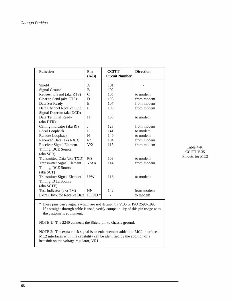
68
Canoga Perkins
Table 4-K.CCITT V.35
Pinouts for MC2
Function Pin CCITT Direction(A/B) Circuit Number
Shield A 101 -Signal Ground B 102 -Request to Send (aka RTS) C 105 to modemClear to Send (aka CTS) D 106 from modemData Set Ready E 107 from modemData Channel Receive Line F 109 from modemSignal Detector (aka DCD)Data Terminal Ready H 108 to modem(aka DTR)Calling Indicator (aka RI) J 125 from modemLocal Loopback L 141 to modemRemote Loopback N 140 to modemReceived Data (aka RXD) R/T 104 from modemReceiver Signal Element V/X 115 from modemTiming, DCE Source(aka SCR)Transmitted Data (aka TXD) P/S 103 to modemTransmitter Signal Element Y/AA 114 from modemTiming, DCE Source(aka SCT)Transmitter Signal Element U/W 113 to modemTiming, DTE Source(aka SCTE)Test Indicator (aka TM) NN 142 from modemExtra Clock for Receive Data FF/DD * - to modem
* These pins carry signals which are not defined by V.35 or ISO 2593-1993. If a straight-through cable is used, verify compatibility of this pin usage with the customer's equipment.
NOTE 1: The 2240 connects the Shield pin to chassis ground.
NOTE 2: The extra clock signal is an enhancement added to -MC2 interfaces.MC2 interfaces with this capability can be identified by the addition of aheatsink on the voltage regulator, VR1.

2240 Fiber Optic Modem
69
The previous V.35 interface Model MC2 / 435, did not conform to the ISO 2593pinout and was the predecessor to the MC2 / 436 interface. The MC2 / 436 wentinto production during mid-summer 1996. The signals listed in Table 4-L havedifferent pinouts on the MC2 / 435 versus the MC2 / 436. The MC2 / 435 also didnot support the Extra Clock for the receive data signal. This pinout differencetable is only included as a reference. MC2 / 436 interfaces can be identified bythe addition of a heatsink on the voltage regulator, VR1.
Table 4-L.Pinout
Differences(MC2 / 435 vs.
MC2 / 436)
4.6.2.1.1 RTS_BIAS JumperThe RTS_BIAS jumper controls the state that RTS floats to when there is no signaldriving the RTS pin. The OFF position forces this signal to the OFF (negated) statewhen the interface cable is disconnected. The ON position forces it to ON (as-serted).
Factory Setting = OFF
Function Pin CCITT Direction(A/B) Circuit Number
Test Mode C C 142 from modem Local Loopback E E 141 to modem Remote Loopback D D 140 to modem

70
Canoga Perkins
4.6.2.1.2 DCD JumperThe DCD jumper determines the source of the DCD output. In the CTRL posi-tion, the DCD output functions as the output for the RTS input at the far end. Inthe CD jumper position and with local RTS ON, CTS will turn ON either when themodem’s fiber optic receiver is in sync (main PCBA internal switch S1 CD /DCD = OFF and CD / SYNC = ON) or the state of the RTS signal at the far end(main PCBA internal switch S1 CD / DCD = ON and CD / SYNC = OFF). Referto Section 2.2.2.1 for more information on the internal switch S1 CD / DCD andCD / SYNC positions.
Factory setting = CTRL
4.6.2.1.3 CTS_GATE JumperThe CTS_GATE jumper controls the state of CTS when the local RTS is ON.When the jumper is in the ON position, CTS follows RTS only. The CD positionallows the 2240's standard data interface signal CD to gate CTS. In the CDjumper position and with local RTS ON, CTS will turn ON either when themodem’s fiber optic receiver is in sync (main PCBA internal switch S1 CD /DCD = OFF and CD / SYNC = ON) or the RTS signal at the far end is ON (mainPCBA internal switch S1 CD / DCD = ON and CD / SYNC = OFF). Refer toSection 2.2.2.1 for more information on the internal switch S1 CD / DCD and CD/ SYNC positions.
Factory setting = ON
4.6.2.1.4 CH_GND JumperThe jumper selects whether chassis ground is connected directly to signal ground(SHORT position) or through a 100 Ohm resistor (100_OHM position).
NOTE: In the standalone model, the 100_OHM position will only put a 100Ohm resistor between the two grounds if the 2240's main board SIGNAL GNDjumper is set to the FLOAT position.
When installed in the 2201 Rack Chassis, any modem main board, interface orrack chassis jumper being set to SHORT will override the FLOAT and100_OHM positions on all of the other modems.
CONSIDER THIS JUMPER CAREFULLY.
Factory Setting = 100_OHM

2240 Fiber Optic Modem
71
4.6.2.2 RS-423 / DB-25 Interface
NOTE: The maximum data rate for this interface is 9.6 Kbps.
This interface is electrically compatible with EIA RS-423A. It will also operatewith asynchronous RS-232D systems.
This interface uses the physical connector type and pinouts specified in RS-232D(refer to Table 4-I). The RS-423 / 232D interface uses a 25-pin, female D-typeconnector for the physical connection. These signal channels operate indepen-dently from the main data channel of the V.35 interface. A worst case samplingjitter of 21 microseconds will be experienced on these channels.
There are six end-to-end control lead pairs. They are listed below with the inputsignal listed first:
TD to RDSTD to SRDDTR to RISRTS to SDCDDSRS to SCTSRTS to DCD
4.7 T1 / E1 Interfaces
4.7.1 Transparent Bipolar - Models 4BX
NOTE: This interface replaces the 4T (1-3) and 4E (1-3) models.It is completely compatible with these previous interface models.
The 4Bx interfaces are compatible with any bipolar, line-coded T1 or E1 data(1.544 or 2.048 Mbps). All types of codes, including AMI, B8ZS, B7S or HDB3,will be accurately transmitted/received. Five DIP switches are used in configuringparticular applications (refer to Table 4-M). Switch positions 1 and 2 select T1 orE1. Positions 3 through 5 select line build out values for T1 usage.

72
Canoga Perkins
Table 4-M.Configuration
Switch Settings
There are three different types of interface connectors, and each is identified bythe number at the end of the interface code of the order number (refer to Table 4-N). The connectors are female DA-15 (4B1); four-position terminal block (4B2);or two female BNCs (4B3). Figure 4-2 shows how the input and output pairs arewired to these connectors.

2240 Fiber Optic Modem
73
This interface performs jitter attenuation of the transmit line input signal. It is alsodesigned to propagate an all "1's" AMI stream if the end-to-end line is interrupted atany point.
When using any of the Transparent Bipolar Interfaces, the 2240 modem rate andmode front panel DIP switches should be set as follows: 1-4 = closed, 5-7 = open(Rate 0, Mode 7). In addition, the first two positions of the internal DIP switch S1must be:CD / DCD = OFF and CD / SYNC = ON. Refer to Section 2.2.2.1.
If the interface signal is lost, Loss of Signal (LOS), the all "1's" Alarm IndicationSignal (AIS) is sent to the other end.
Factory Setting = Both jumpers are OFF
These interfaces allow full inter-operation with any of the synchronous data inter-faces when the customer's T1/E1 is AMI-coded (see Figure 4-3). This interface willnot inter-operate with synchronous data interfaces if the T1 / E1 is B8ZS or HDB3.
Two jumper straps are provided for setting the line termination impedance to either100 ohm for T1 or 120 ohm for E1 applications. These straps are located near themiddle of the interface board and are provided only for the 4B1 and 4B2 versions.For the 4B3 version (BNC connectors) the termination impedance is fixed at 75ohms.
Table 4-N.TransparentBipolar Line
Interfaces
Model # Interface SpeedConnectorType
4B1 DA-15 1.544 Mhz T1 or 2.048 Mhz E14B2 Terminal Block 1.544 Mhz T1 or 2.048 Mhz E14B3 BNC (75 ohm) 1.544 Mhz T1 or 2.048 Mhz E1
These interfaces are fully transparent to line codes such as B8ZS or HDB3.Three DIP switches (3, 4 and 5) are provided for selecting various line buildout settings as indicated in Table 4-M. Standard factory settings are T1 at0-133 feet for all three models. Two DIP switches (1 and 2) are provided toselect CCITT speed (2.048 Mhz) or T1 speed (1.544 Mhz).

74
Canoga Perkins
T1
2240(mode 7)
2240(mode 5 Slave)
V.35
Rx
Tx
DataClk Tx
DataClk Rx
4B1
436
Figure 4-2.Transparent BipolarInterface Connectors
Figure 4-3.Example of LinkBetween Bipolar
and ClockedInterface

2240 Fiber Optic Modem
75
4.8 TTL / BNC Interface Model -BNThis model uses BNC (bayonet) connectors for the physical interface. The electricalsignal characteristics are unbalanced TTL levels, with only the clock and datacircuits supported. Four BNC connectors are supplied for connection to a DTEdevice.
High speeds and long distances (clock and data only) can be achieved using thisinterface.
This interface version has a switchable dual purpose port for the Send Timing (SCT)and Terminal Timing (SCTE) clock signals. A two-position slide switch (S1) on theinterface card controls the port direction.
Figure 4-4.BNC Connectors
When the switch is set towards the BNC connectors, the port is configured as an input(for the SCTE clock). Sliding the switch away from the BNC connectors configuresthe port as an output (for the SCT clock). (See Figure 4-4 for connectors and refer toTable 4-O for signals supported.)
NOTE: When setting up the clock select, the proper main circuit boardclock mode must be set correctly, i.e., external for the SCTE clock input,slave or internal for the SCT clock output.

76
Canoga Perkins
4.9 Programmable Buffered Interface / Model P53
Signal Full Name Direction
TxD Transmit Data To ModemRxD Receive Data From ModemSCR Serial Clock Receive From ModemSCT Serial Clock Transmit From ModemSCTE External Clock Transmit To Modem
Table 4-O.BNC Supported
Signals
The Model P53 Interface Module complies with EIA Standard RS-530 while allclock, data and control signals follow the RS-422 standard. The basic configura-tion of the P53 interface is a DCE device (w/Fem DB-25) and two connectoradapters are provided with the interface: the DCE / DTE adapter which convertsthe interface to the DTE form (w/Male DB-25) and the "Legacy" adapter whichconverts the interface to the original Model P2 interface.
This interface implements a set of circuits (resources) which can be interconnectedin various ways to satisfy a host of differing applications. These resources are:
• a 16-bit FIFO (first-in, first-out) buffer• an inverter• a switchable delay line
The FIFO can be utilized to buffer either the received or the transmitted data (notboth). The Delay Line, in conjunction with a four-position DIP switch, provides anoption for fine tuning the relationship between clock and data timing. Table 4-Pdefines the delay lines versus switch settings for the Model P53 Interface.
2240 Fiber Optic Modem
77
A wire wrap header (J3) provides the means to interconnect these resourcestogether with the standard modem transmit and receive circuits to perform theintended function. Figure 4-5 illustrates how the resources are tied into the J3header. Specific applications are satisfied by wire wrap connections betweenappropriate pins.
Four pre-wrapped headers are provided with the interface. These implementthe most common applications. See Figures 4-7, 4-9,4-11 and 4-13. Numer-ous other configurations are possible by different wired versions of the header,P3. The four versions included are identified by part number labels affixed tothe underside of the header. The version included in the socket as shipped isP/N 610030-001 (see Figure 4-13).
The P53 can be used to interface with encryption devices on the BLACK sidewhere modems act as the network and supply clocking in a synchronousconfiguration, or to the RED (clear) side of a data encryption (KG) equipment.In the RED side application, the interface acts as the "tail-circuit adapter"device. This configuration allows the modem to accept two synchronousclocks (typically, DCE devices only accept one): one for transmit (externalclock) and one for receive (FIFO input clock).
Another common application is with systems that communicate over geosyn-chronous satellites. In this application, the FIFO is used to make up for clockdrift (Doppler shift) caused by the satellite's elliptical orbit around the earth.

78
Canoga Perkins
Figure 4-5.Available Strapping
Options forProgrammable
Buffered Interface
KG Swing
Jumpers
Internal
Clock From
Modem
Rx Data
Tx Clock
Tx Data
Modem
Alarm
From
Fiber
To
Fiber
Delay
Line
Inverter
FIFO
Data Out Data In
Shift Out Shift I n
Wire
Wra
p H
eade
r J3
W19
W20
8
SG
FG
CTS
DSR
RTS
FIFO
Clock
SCTE
TxDxD
From Modem
To Modem
To Modem
10
3
16
17
9
15
12
5
12
19
13
14
16
17
18
3
4
9
6
1
2
11
10
15
7
8
20
23
24
11
2
14
LL
RL
SCT
RLSD
RxD
SCR
IN
OUT
J1(D
B -
25)
7
1
5
13
22
19
18
21
6
4
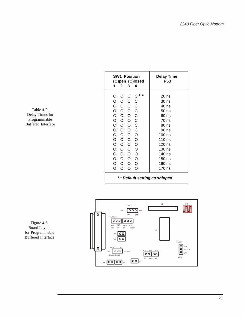
2240 Fiber Optic Modem
79
Table 4-P.Delay Times forProgrammable
Buffered Interface
Figure 4-6.Board Layout
for ProgrammableBuffered Interface
W8 W9 W7
W14 W13 W12
-6V +/-6V +6V
100 ohm
CHASSIS GND
W2
W1SHORT
J3
RSTBIAS
OFF ON KG NORMW18 W17
W6
W5
W19 W20
Test GND
DSR
W16W15
Dl1 Sw1
W10
W11
INVERT
NORM
KG OUT
SW1 Position Delay Time(O)pen (C)losed P531 2 3 4
C C C C * * 20 nsO C C C 30 nsC O C C 40 nsO O C C 50 nsC C O C 60 nsO C O C 70 nsC O O C 80 nsO O O C 90 nsC C C O 100 nsO C C O 110 nsC O C O 120 nsO O C O 130 nsC C O O 140 nsO C O O 150 nsC O O O 160 nsO O O O 170 ns
* * Default setting as shipped

80
Canoga Perkins
Table 4-R.Strap
Configurationsfor RLSD (CD)
Output
The W1 / W2 strap connects chassis ground to signal ground (W2 position), connects chassisground through 100 ohms to signal ground (W1 position), or isolates chassis ground from signalground (jumper out). The W5, W6 and W7 jumpers, when installed, ground the midpoints of the100 ohm termination resistances of the FIFO CLK, SCTE and TxD line receivers. These jump-ers may provide improved performance in cases where the RS-422 inputs are bipolar ratherthan the more common unipolar types. The W8, W9 and W15 / W16 jumpers are used forconverting to the Legacy configuration (see Figure 4-15).
4.9.1 Jumper SettingsAll jumper settings and descriptions are listed in Table 4-Q. This interface has strap optionjumpers to configure the RLSD Output at J1-8 (DB-25) to support the KG-194 Resync function-ality. Jumper straps W10 / W11 (adjacent to U11) and W12 / W13 / W14 (adjacent to U8)implement this function (refer to Table 4-Q and Figure 4-6). Jumper straps W10 / W11 controlthe ON / OFF level and W12 / W13 / W14 configure the RLSD Output to Bipolar (+6 V and -6 V)or single-ended (+6 and 0 or -6 and 0).
Table 4-Q.Jumper Settingsand Descriptions
STRAP CONFIGURATIONS CD OUTPUT (AT J1-8 * * )VOLTAGE LEVEL ±1 V
ON/OFF
W11 and W14 +6/-6W11 and W12 +6/0W11 and W13 0/-6W10 and W14 -6/+6W10 and W12 0/+6W10 and W13 -6/0
* * J1-6 when using the "Legacy" (P2) Converter
Jumper Description Notes FactorySetting
W1 / W2 Chassis Ground W1 - 100 ohms / W2 - Short W1 Default W5, W6, W7 RCVR Terminations All Out W8 / W9 Legacy Config. Both Out W10 / W11 RLSD Output Swing W11 W12 / W13 / W14 RLSD Output Swing W13 W15 / W16 DSR W15 - Test / W16 - GND W16 Default W17 / W18 RTS Bias W17 - On / W18 - Off W18 Default W19 / W20 RLSD W19 - Single Ended / W20 Default
W20 - Differential

2240 Fiber Optic Modem
81
4.9.2 Generic InterfaceFigure 4-7 illustrates basic DCE configurations, which bypass all the "feature"circuits provided by the P53 Interface.
Figure 4-7.Programmable
Buffered Interface,Model P53, Basic
DCE RS-530
KG Swing
Jumpers
Internal
Clock From
Modem
Rx Data
Tx Clock
Tx Data
Modem
Alarm
From
Fiber
To
Fiber
Delay
Line
Inverter
FIFO
Data Out Data In
Shift Out Shift I nW19
W20
8
SG
FG
CTS
DSR
RTS
FIFO
Clock
SCTE
TxDxD
From Modem
To Modem
To Modem
10
3
16
17
9
15
12
5
12
19
13
14
16
17
18
3
4
9
6
1
2
11
10
15
7
8
20
23
24
11
2
14
LL
RL
SCT
RLSD
RxD
SCR
IN
OUT
J1(D
B -
25)
7
1
5
13
22
19
18
21
6
4
P/N 6100030-006
Wire Wrap
6-13
7-17
8-18
9-19
14-15
Net List
PROGRAMMABLE BUIFFERED INTERFACEMODEL P53, GENERIC DCE RS-530
P/N 6100030-006

82
Canoga Perkins
4.9.3 External StationThe External Station is used when an external station clock is providing timing (seeFigures 4-8 and 4-9). When connecting KG or KIV encryptors together on theBlack side, using an external timing device you should install the external stationclock strapped header in the J3 position. In this application, the modems are actingas the network, although the timing input is from an outside source. The modem inwhich the timing source is connected should be set for external and the other modemset for slave. This header is provided with the interface.
Figure 4-9.Programmable
Buffered Interface,Model P53,
External Station
Figure 4-8.External StationProgrammable
Buffered Interface,Model P53,
DCE RS-530
Typical External Station Clock Application
KG Swing
Jumpers
InternalClock From
Modem
Rx Data
Tx Clock
Tx Data
Modem
Alarm
From
Fiber
ToFiber
Delay
Line
Inverter
FIFO
Data Out Data In
Shift Out Shift I nW19
W20
8
SG
FG
CTS
DSR
RTS
FIFO
Clock
SCTE
TxDxD
From Modem
To Modem
To Modem
10
3
16
17
9
15
12
5
12
19
13
14
16
17
18
3
4
9
6
1
2
11
10
15
7
8
20
23
24
11
2
14
LL
RL
SCT
RLSD
RxD
SCR
IN
OUT
J1(D
B -
25)
7
1
5
13
22
19
18
21
6
4
Wire Wrap
3-6
4-9
5-7, 14 & 17
8-18
12-19
Net List
P/N 6100030-004
CANOGAPERKINS
Data
Rx Tx
Clock
Rate mode
PwrLoop
OnRem/Loc
2270
Fiber
Modem
Optics
TXRX
Off
CANOGAPERKINS
Data
Rx Tx
Clock
Rate mode
PwrLoop
OnRem/Loc
2270
Fiber
Modem
Optics
TXRX
Off
MM or SM
Fiber Optics
KG/KIV
RED BLK
Station
Clock
KG/KIV
REDBLK
P/N 6100030-004

2240 Fiber Optic Modem
83
4.9.4 InternalThe internal function is used when network equipment is set for Eternal Timing (seeFigures 4-10 and 4-11). When connecting KG or KIV encryptors together on the Blackside, you should install the internal strapped header in the J3 position. In this applica-tion, the modems are acting as the network timing source. In most cases, both modemsshould be set for internal master clock. The rate switches should be set to the appropri-ate speed for the circuit. This header is provided with the interface.
Figure 4-11.Internal
ProgrammableBuffered Interface,
Model P53
KG Swing
Jumpers
InternalClock From
Modem
Rx Data
Tx Clock
Tx Data
Modem
Alarm
From
Fiber
ToFiber
Delay
Line
Inverter
FIFO
Data Out Data In
Shift Out Shift I nW19
W20
8
SG
FG
CTS
DSR
RTS
FIFO
Clock
SCTE
TxDxD
From Modem
To Modem
To Modem
10
3
16
17
9
15
12
5
12
19
13
14
16
17
18
3
4
9
6
1
2
11
10
15
7
8
20
23
24
11
2
14
LL
RL
SCT
RLSD
RxD
SCR
IN
OUT
J1(D
B -
25)
7
1
5
13
22
19
18
21
6
4
P/N 6100030-005
Wire Wrap
6-13
7-17
8-18
9-19
10-14
11-15
Net List
CANOGAPERKINS
Data
Rx Tx
Clock
Rate mode
PwrLoop
OnRem/Loc
2270
Fiber
Modem
Optics
TXRX
Off
CANOGAPERKINS
Data
Rx Tx
Clock
Rate mode
PwrLoop
OnRem/Loc
2270
Fiber
Modem
Optics
TXRX
Off
MM or SM
Fiber Optics
KG/KIV
RED BLK
KG/KIV
REDBLK
P/N 6100030-005
Typical Internal Clock Application
Figure 4-10.Internal
ProgrammableBuffered Interface,
Model P53,DCE RS-530

84
Canoga Perkins
4.9.5 ExternalThe External function is used when network equipment is set for Network or Inter-nal Timing (see Figures 4-12 and 4-13). When connecting KG or KIV encryptorson the Red side to a DTE device, you should install the external strapped header inthe J3 position. In this application, the modems are acting as an extension of the Redside cable in a true tail circuit. The modem at the Red end is set for external clockand the modem at the DTE end is set for slave clock. This header is provided withthe interface.
Figure 4-13.External
ProgrammableBuffered Interface,
Model P53
Figure 4-12.External
Programmable Buff-ered Interface, Model
P53, DCE RS-530
KG Swing
Jumpers
InternalClock From
Modem
Rx Data
Tx Clock
Tx Data
Modem
Alarm
From
Fiber
ToFiber
Delay
Line
Inverter
FIFO
Data Out Data In
Shift Out Shift I nW19
W20
8
SG
FG
CTS
DSR
RTS
FIFO
Clock
SCTE
TxDxD
From Modem
To Modem
To Modem
10
3
16
17
9
15
12
5
12
19
13
14
16
17
18
3
4
9
6
1
2
11
10
15
7
8
20
23
24
11
2
14
LL
RL
SCT
RLSD
RxD
SCR
IN
OUT
J1(D
B -
25)
7
1
5
13
22
19
18
21
6
4
P/N 6100030-001
Wire Wrap
3-6
4-9
5-16
7-17
8-18
12-19
Net List
CANOGAPERKINS
Data
Rx Tx
Clock
Rate mode
PwrLoop
OnRem/Loc
2270
Fiber
Modem
Optics
TXRX
Off
CANOGAPERKINS
Data
Rx Tx
Clock
Rate mode
PwrLoop
OnRem/Loc
2270
Fiber
Modem
Optics
TXRX
Off
MM or SM
Fiber Optics
KG/KIV
REDBLKDTE
P/N 6100030-001

2240 Fiber Optic Modem
85
4.9.6 DTE AdapterThis adapter is supplied with the P53 interface and should be used when connecting toa DCE device. This allows the use of a straight-through RS-530 cable. Figure 4-14illustrates the DCE to DTE pin assignments. The gender of this adapter on the userside is male.
Figure 4-14.Programmable
Buffered Interface,Model P53 [DTE]
PROGRAMMABLE BUFFERED INTERFACE
MODEL P53, DCE RS-530 [DTE]
SG
FG
CTS
7
1
8
RLSD
RxD
10
3
16
17
9SCR
15
12SCT
FIFO
CLOCK
20
23
24
11
2
14
SCTE
TxD
5
13
6
22
4
19
DSR
RTS
LL
RL
MODEM
ALARM
DTE ADAPTER
4
19
2
14
24
11
15
12
17
9
3
16
7
1
NC
NC
NC
NC = NOT CONNECTED

86
Canoga Perkins
4.9.7 Legacy AdapterThis adapter is provided with the P53 interface and should be used if preexistingcabling was installed for use with Model P2 interface cards (see Figure 4-15). Thisadapter converts the standard RS-530 pin assignment on the P53 back to the originalP2 pin assignments.
PROGRAMMABLE BUFFERED INTERFACE
MODEL P53, DCE RS-530 [LEGACY]
SG
FG
CTS
7
1
8RLSD (RS-423)
RxD
3
16
17
9SCR
15
12SCT
FIFO
CLOCK
20
23
24
11
2
14
SCTE
TxD
5
13
6
22
4
19
DSR
RTS
LL
RL
MODEM
ALARM
LEGACY ADAPTER
6
20
21
9
10
12
13
17
18
3
4
14
15
7
1
2
5
8
16
22
25
11
W9W8
W15/W16 MUST BE SET TO W15
W8-IN CONNECTS PINS
2,5,8,11,16,22 AND 25 TO
SIGNAL GROUND
W9-IN CONNECTS PINS
2,5,8,11,16,22 AND 25 TO
CHASSIS GROUND
Figure 4-15.Programmable
Buffered Interface,Model P53
[Legacy Adapter]

2240 Fiber Optic Modem
87
4.10 High-Speed RS-422 / Mil-Std 188-114C InterfacesThere are three High-Speed RS-422 interface models (TW, T22 and D22) and threeHigh-Speed Mil-Std 188-114C interface models (TW8, T88 and D88) available.
All can operate up to 20 Mbps (2240 limited to 2.048 Mbps). All support onlyclock and data signals as shown in Table 4-R. Both the RS-422A and Mil-Std 188-114C are balanced differential electrical signals.
Signal Full Name Direction
TxD Transmit Data To ModemRxD Receive Data From ModemSCR Serial Clock Receive From ModemSCT Serial Clock Transmit From ModemSCTE External Clock Transmit To Modem
Table 4-S.TwinAx
SupportedSignals
The RS-422A operates between +1 and +4 volts whereas the Mil-Std 188-114Cswings between +/-3 volts. The termination impedances vary slightly as illustratedin Table 4-T. The two interface types will communicate with each other butcenter tap ground jumpers E2 and E3 must be removed from a Mil-Std 188-114Cinterface (refer to Table 4-U).
The basic differences between the models is the type of physical connectors usedfor the interface. Table 4-T lists the six interface models with the correspondingsource and termination impedances and physical connectors. Table 4-U shows thejumper options available and the factory default settings for the jumpers.
4.10.1 Model TWThe signaling used on this interface is RS-422A. Four TwinAx connectors (BJ-77, 3-lug) are used for the physical connection (see Figure 4-16).
A switch is provided to select whether the fourth TwinAx (SCT / SCTE) is to beused as an output (SCT) or as an input (SCTE). By setting the switch to the SCTposition, the port becomes an output providing the clock to the connected device.When set for SCTE, the port becomes an input and will accept a clock from theconnected device.

88
Canoga Perkins
SCT should be selected if the modem is set for Internal or Slave Clock mode.SCTE should be selected if the modem is set for External Clock mode.
NOTE: The SCT output cannot be returned on the SCTE leads toeliminate propagation delay problems with this interface.
Table 4-T.Model
Characteristics
TW RS-422A 4 TwinAx Figure 4-16 <100 Ohms 100 Ohms ±10%
TW8 Mil-Std 4 TwinAx Figure 4-16 <100 Ohms 78 Ohms ±10% 118-114C
T22 RS-422A 5 TwinAx Figure 4-17 <100 Ohms 100 Ohms ±10%
T88 Mil-Std 5 TwinAx Figure 4-17 <100 Ohms 78 Ohms ±10% 188-114C
D22 RS-422A DC-37 Table 4-V <100 Ohms 100 Ohms ±10%
D88 Mil-Std DC-37 Table 4-V <100 Ohms 124 Ohms ±10% 188-114C
Model Electrical Physical Physical Driver TerminationInterface Interface Interface Impedance ImpedanceType Type Figure /
Table

2240 Fiber Optic Modem
89
Table 4-U.Jumper Strap
Options
JUMPER DESCRIPTION FACTORY CONFIGURATION ID TW TW8 T22 T88 D22 D88
W3 / W4* W3 = VCO disabled W4 W4 W4 W4 W4 W4 W4 = VCO enabled
W5 / W6** W6 = Normal SCT W6 W6 W6 W6 W6 W6 W5 = Inverted SCT
W5 / W6 W7 = Shield connected to W7 W7 W7 W7 W7 W7 chassis ground W8 = Shield connected to signal ground
W9 / W10 W9 = Chassis ground W10 W10 W10 W10 W10 W10 connected to signal ground W10 = Not connected
E2 TxD RCV termination N/A IN N/A IN N/A IN resistor
E3 SCTE RCV termination N/A IN N/A IN N/A IN resistor center tap to shield ground
* W3 / W4 jumper option may not exist on some older versions. It is only required when performing Local loopbacks. The W4 position corrects the duty cycle of External Clock above 9 Mbps.** The W5 / W6 jumper option serves the same function as the SCT Normal / Invert Jumper on the main 2240 board. Either one may be used to invert SCT. Refer to Section 2.2.5 for details.

90
Canoga Perkins
4.10.2 Model TW8The signaling used on this interface is Mil-Std 188-114C. Four TwinAx connec-tors (BJ-77, 3-lug) are used for the physical connection (see Figure 4-16).
A switch is provided to select whether the fourth TwinAx (SCT / SCTE) is to beused as an output (SCT) or as an input (SCTE). By setting the switch to the SCTposition, the port becomes an output providing the clock to the connected device.When set for SCTE, the port becomes an input and will accept a clock from theconnected device.
SCT should be selected if the modem is set for Internal or Slave Clock mode.SCTE should be selected if the modem is set for External Clock mode.
NOTE: The SCT output cannot be returned on the SCTE leads toeliminate propagation delay problems with this interface.
Figure 4-16.Four TwinAxConnectors
(BJ-77, 3-Lug)

2240 Fiber Optic Modem
91
4.10.3 Model T22The signaling used on this interface is RS-422A. Five TwinAx connectors (BJ-77,3-lug) are used for the physical connection (see Figure 4-17).
4.10.4 Model T88The signaling used on this interface is Mil-Std 188-114C. Five TwinAx connec-tors (BJ-77, 3-lug) are used for the physical connection (see Figure 4-17).
4.10.5 Model D22The signaling used on this interface is RS-422A. A standard 37-position, D-typefemale connector (DC-37) is used as the physical connection (refer to Table 4-V).
4.10.6 Model D88The signaling used on this interface is Mil-Std 188-114C. A standard 37-position,D-type female connector (DC-37) is used as the physical connection (refer toTable 4-V).
Figure 4-17.Five TwinAxConnectors
(BJ-77, 3-Lug)

92
Canoga Perkins
Table 4-V.Models D22 andD88 Connector
Pin Assignments
*

2240 Fiber Optic Modem
93
4.11 Interface ReconfigurationFigure 4-18 illustrates how the interface circuit board fits into the larger mainmodem board opening.
A header-type connector is provided to connect the two circuit boards together.The interface board may be removed by loosening the two retaining screws andnuts, then pulling the board outward from its connector.
Once a replacement board is in position, the two flanged lock nuts and screws aresecured with built-in flat washers above and below the board junctures.
It may be desirable to select a new data rate at this time using the front panelswitches as outlined in Chapter 3 of this manual.
Figure 4-18.Interface Card
Installation
Retaining Screw
Retaining Screw

94
Canoga Perkins
4.12 Standalone ReconfigurationTo access the circuit board on a standalone unit, the enclosure cover must first beremoved by loosening the six screws on the sides of the unit. Next, unplug thepower supply connector from the PC board, and remove the two screws holdingthe rear panel in place.
The entire circuit board may now be removed by loosening the eight mountingscrews. The interface board may now be changed as outlined in Section 4.11,"Interface Reconfiguration."
The rear panel supplied with the new interface must also be exchanged with theoriginal rear panel. The unit may then be assembled in the reverse order of thedisassembly.

2240 Fiber Optic Modem
95
5. Troubleshooting
5.1 Diagnostic ProceduresThe following procedures are intended for use in the event of a system failure, notduring the initial installation of a 2240 optical link. For initial installation checkout,refer to Section 1.7 of this manual. Also, refer to Section 6 for detailed diagnostics.
5.2 Local and Remote Loopback
5.2.1 Loopback TestsAll 2240s have built-in Local and Remote Loopback. These tests can be used toverify the basic operation of a 2240 system.
The test modes can be activated by setting the Loopback switch on the front panel orby turning on the Local Loopback or Remote Loopback control leads in the electricalinterface (supported interfaces only). See Section 4 for more information.
Whenever either modem has a Loopback selected, the Loop On indicators on bothmodems will be on and the DSR signal on the interface may be negated (checkstrapping of interface). Figure 5-1 shows a local loopback configuration.
HOSTTERMINAL HOSTTERMINAL
USERTERMINAL
TX
RX
RX
TX
LOOPLEDON
LOCALLOOP
LOOPLOCAL
SYNC
SYNC
LOOPOFF
LOOPLEDON
FIBER OPTIC LINK
Figure 5-1.Local Loopbackfrom User-Endof Fiber Link

96
Canoga Perkins
NOTE: Interface control of the loopback tests is only supported on thefollowing modular interfaces: RS-423 / RS-232C, RS-449, RS-530 andV.35.
When activated, the Local Loopback test will cause all data transmission from the nearend (local) user device to be looped back toward the receive of that same device. Thedata from the remote user device will not loop back (it will continue receiving datafrom the local device), but the Loop On indicator at the far end turns on.
The loopback point is set at the electrical interface of the local modem (see Figure 5-1).
NOTE: If the local loopback modem is operating in Mode 5 (slave clockmode), the remote device will receive garbled data because of the overalltiming configuration. The local loopback will function correctly.
5.2.2 Remote Loopback TestWhen activated, the Remote Loopback test will cause all data transmission from thenear end (local) user device to be looped back after the optical sections of the remotedevice.
The data from the remote user device also loops back locally at the electrical interface.See Figure 5-2.
HOSTTERMINAL HOSTTERMINAL
USERTERMINAL
TX
RX
RX
TX
LOOPON
LOOPREMOTE
SYNC
SYNC
LOOPOFF
LOOPON
FIBER OPTIC LINK
REMOTELOOP
Figure 5-2.Remote Loopback
from User-Endof Fiber Link

2240 Fiber Optic Modem
97
6. Diagnostic Procedures
6.1 2240 / 2201 Diagnostic ProceduresThe following diagnostic procedures should be followed to test the 2240 system,troubleshoot a defective link or detect a defective fiber optic cable, connector,modem or power supply.
NOTE: Refer to the 2201 Rack Chassis / 2200R Redundant ModemCard User Manual for diagnostic procedures for the 2201 RackChassis and power supplies.
6.1.1 Required Equipment1) Multimeter - for AC voltage, resistance and continuity tests2) Fiber Optic Power Meter - should be calibrated atthe correct optical wave
length with the appropriate optical connectors3) A short (one meter or less) fiber optic jumper cable consistent with the
modem optics under test, terminated with the appropriate connectors4) A Bit Error Rate Tester (BERT) with the appropriate electrical interface and
cable
Step Symptom Possible Cause(s) Action
1 No power indicator No AC power Check ACon front panel(s) power
source
2 No power indicator Defective modem Replaceon front panel(s) Modem
NOTE: Once any power system problems have been corrected,continue the system checkout after the Loopback DiagnosticProcedure.

98
Canoga Perkins
6.2 Loopback Test Diagnostic Procedure
Step Symptom Possible Cause(s) Action
1 No Sync Indication. Defective fiber optic Continue to themodem(s), cable(s) to the next step.or connectors. If themodems are con-figured for a tail circuit(one is externallylocked and the otheris slave), verify that theexternally locked 2240has a clock on its TT(or equivalent) leadsthat matches its rateswitch.
2 Verify the optical cable loss. Remove the Tx fiber from the modem. Usethe optical power meter and fiber optic jumper cable to determine theoptical launch power for this modem. Reconnect the Tx fiber to themodem. Remove the Rx fiber from the modem and determine the opticalreceive power into this modem. Reconnect the Rx fiber to the modem.Repeat the above step for the modem at the other end and record bothoptical power levels.
Perform the following optical loss calculation:Near-end Receiver level minus far-end Transmit level = Near-end linkloss figure.Far-end Receiver level minus near-end Transmit level = Far-end link lossfigure.
If the optical cable loss figure exceeds the optical link loss budgetspecified for the modem, set the optical launch power for the modem(s)to the high power setting and repeat the power measurements (refer to the"Specifications" section for appropriate loss budget figures). If the actualcable loss still exceeds the loss budget for the modem, go to Step 3. Ifthe cable loss is within the specified loss budget for the modem, go toStep 5.

2240 Fiber Optic Modem
99
Step Symptom Possible Cause(s) Action
3 Cable loss exceeds Defective Repair ormodem loss budget. F/O cable replace defective
cable
4 Cable loss exceeds Defective Fiber Repolish ormodem loss budget. Optic Connectors replace defective
connector
5 Set the Remote Loopback switch on the near-end modem. Set up BERTtester for the proper clocking, data rate and format as used with thecircuit. Use the existing interface cables if possible. Connect the BERTtester in place of the near-end user device. Run the BERT test and go tothe next step.
6 Loopback test passes Modem not Verify / correctbut modems will not configured switch and strappass data. properly settings on modem
and devices
7 Loopback test passes Interface cables Repair damaged orbut modems will not damaged or mis- miswired cablespass data. wired.
8 Optically loopbackeach modem and repeatBERT test as detailed inStep 5 of this procedure.
Modem fails BERT Defective modem or Replace defectivetest when optically electrical interface modemlooped back to itself.
9 Set the Local Loop-back switch on thenear-end modem.
Modem fails BERT Defective modem or Replace defectivewhen looped locally electrical interface modem

100
Canoga Perkins
Table 6-A. Link Loss Range
6.3 Fiber Optic Diagnostic ProcedureIf the Loopback Test is successful, and the modems still do not function, check thefiber optic parameters as outlined below. There also may be a data rate incompat-ibility. If this check out of the electrical and optical links provides no indication asto the problem, contact Canoga Perkins Installation and Repair Department for as-sistance.
NOTE: Each range limit has a +1dB margin at the transition point.
The following are some additional checkpoints to consider:••••• Fiber optics.
••••• Are you using a fiber optic link of less than the High Power LossBudget? (refer to Table 6-A)
Set the optical power switch to LO.••••• Are you using a fiber optic link of more than the Low Power Loss
Budget?(refer to Table 6-A)Set the optical power switch to HI.••••• Are the fiber optic cables marked correctly?Connect Tx cable to Tx connector, Rx to the Rx connector.If Local and Remote Sync indicators do not come on, try swapping cablesat one end of link.••••• Is the data rate set correctly?••••• Are you using the correct clock mode (internal/external) for
synchronous transmission or are you using asynchronoustransmission?
NOTE: The 1310 nm LP Laser does not have a HI/LO power switch.
Link Loss Range
Model HI Power LO Power
850 nm Standard >6 dB to Max <6 dB1310 nm HP Laser >6 dB to Max <6 dB1550 nm HP Laser >6 dB to Max <6 dB1310 nm LP Laser – –
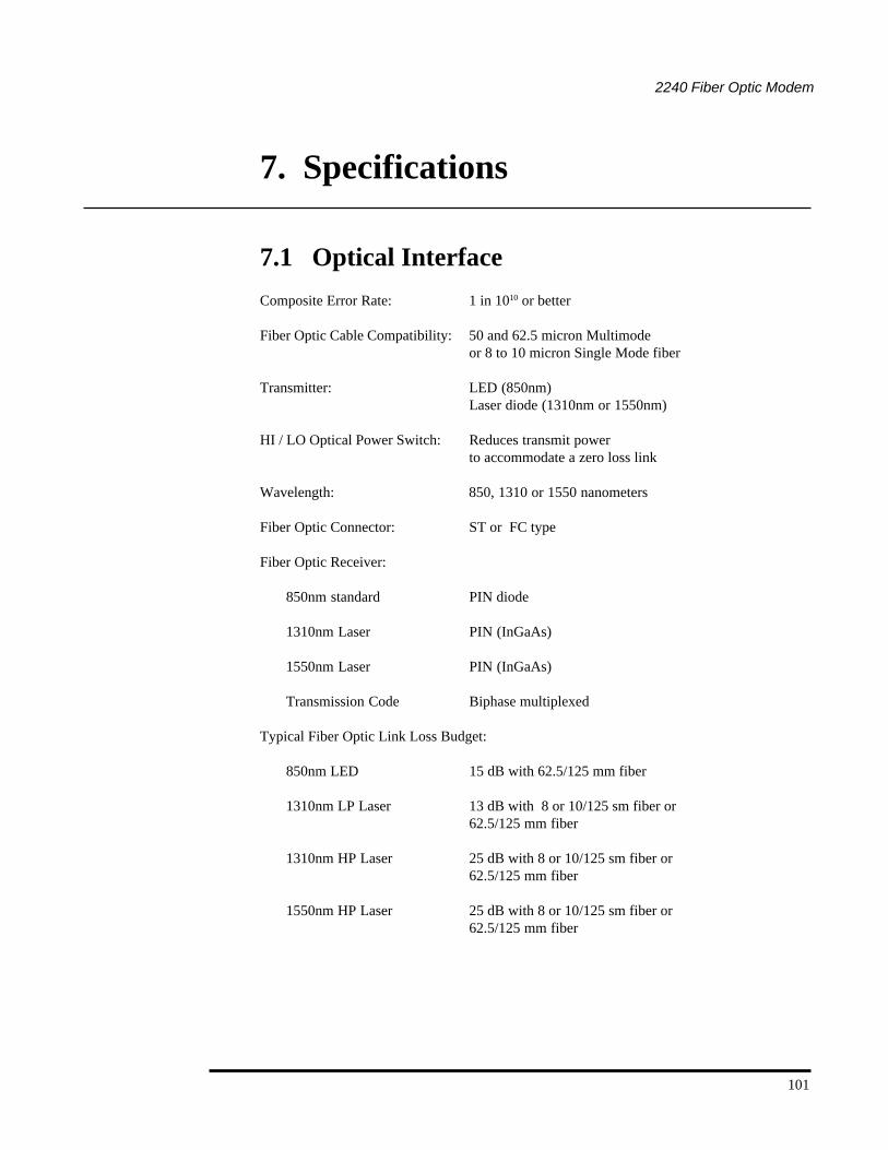
2240 Fiber Optic Modem
101
7. Specifications
7.1 Optical InterfaceComposite Error Rate: 1 in 1010 or better
Fiber Optic Cable Compatibility: 50 and 62.5 micron Multimodeor 8 to 10 micron Single Mode fiber
Transmitter: LED (850nm)Laser diode (1310nm or 1550nm)
HI / LO Optical Power Switch: Reduces transmit powerto accommodate a zero loss link
Wavelength: 850, 1310 or 1550 nanometers
Fiber Optic Connector: ST or FC type
Fiber Optic Receiver:
850nm standard PIN diode
1310nm Laser PIN (InGaAs)
1550nm Laser PIN (InGaAs)
Transmission Code Biphase multiplexed
Typical Fiber Optic Link Loss Budget:
850nm LED 15 dB with 62.5/125 mm fiber
1310nm LP Laser 13 dB with 8 or 10/125 sm fiber or62.5/125 mm fiber
1310nm HP Laser 25 dB with 8 or 10/125 sm fiber or62.5/125 mm fiber
1550nm HP Laser 25 dB with 8 or 10/125 sm fiber or62.5/125 mm fiber

102
Canoga Perkins
7.2 System ElectricalInterface Connector:
Interface Connector Type
RS-232C / 423 / 530 female DB-25Programmable RS-530 (P53) female DB-25RS-422 (422) female DC-37CCITT V.35 (V.36) female 34-pin WinchesterTTL / BNC four female BNC coaxialRS-422, Mil-Std 188-114C four or five female Twinaxial connectors, BJ-77 (3-lug)
Transparent T1 / E1 female DA-15, two female BNCs or Terminal strip
Interfaces Supported: RS-232D / RS-423RS-449CCITT V.35TTL / BNCProgrammable RS-422 (P)TwinAx 422TwinAx MIL-STD-188-114CDC-37 MIL-STD-188-114Transparent T1 / E1CCITT V.35 / RS-423 (MC2), RS-449 / 423 (MC1)RS-530
TYPICAL LAUNCH POWER AND Rx SENSITIVITY
LAUNCH POWER (dBm)
OPTIC TYPE HI LO Rx SENS. (dBm)
850 LED -15±2 -20±4 -32
1310 LP LASER -15±2 -15±2 -32
1310 / 1550 HP LASER -5±1 -14±2 -32
Table 7-A.Launch Power and
Rx Sensitivity

2240 Fiber Optic Modem
103
Power Requirement:
Standalone 115 VAC +10% @ 0.22 Amps115/230 VAC + 10% switchable@ 0.11 Amps ,47 to 63 Hz-48VDC; 0.5 Amps (max)
Rack Mount PC Card 18 VAC +10% @ 1.1 Amps per board50 to 64 Hz
7.3 Indicators and ControlsIndicators (6): Tx/Rx Data Activity; Local / Remote Sync;
Loopback Active; Power On;Power Alarms (2201 Rack Only)
Controls (10): Local / Remote Loopback Slide Switch;Operating Mode DIP Switch; Data Rate DIPSwitch; Hi / Low Optic Power DIP Switch
7.4 Physical / Environmental:Dimensions:
2240-S Standalone 12.8" L x 8.5" W x 2.5" HPC Card 12.5" L x 7.8" W x 1.06" H
Unit Weights [shipping]:2240-S Standalone 3.63 lbsPC Card 0.9 lbs
Operating Environment:Temperature 0 to 50 0CHumidity 0 to 95% (non-condensing)

104
Canoga Perkins
7.5 2240 Fiber Optic Modem Configurations 2240-S-XXX-XX-XX-X S = STANDALONE 2240-R-XXX-XX-XX-0 R = RACKMOUNT
POWER OPTIONS0 - N/A1 - 115V-AC WALL PLUG2 - 115/230V IN-LINE3 - 48VDC (Call Canoga Perkins for additional DC options)
CRYSTAL OPTIONS00 - NO CRYSTAL
The 2240 Fiber Optic Modem provides most standard clock rateswith built in oscillators. If a non-standard internal clock rate isrequired, refer to Section 3.3, or call Canoga Perkins and ask forApplications Support.
FIBER OPTIONS MULTIMODE (STANDARD)01 - 850nm LED ST11 - 1310nm LASER ST13 - 1310nm LASER FC16 - 1310nm LP LASER ST17 - 1310nm LP LASER FC
SINGLE MODE (STANDARD)11 - 1310nm LASER ST13 - 1310nm LASER FC16 - 1310nm LP LASER ST17 - 1310nm LP LASER FC21 - 1550nm HP LASER ST23 - 1550nm HP LASER FC
INTERFACE OPTIONS432 EIA 423 / EIA 232 / DB-25 w/ Control422 EIA 422 / DC-37 w/ Control430 EIA 530 / DB-25435 V.35 / MRC-34 w/ Control (Special Situations Only)436 V.35 / MRC-34 w/ Control4B1 1.544 / 2.048 T1 / E1 DA-154B2 1.544 / 2.048 T1 / E1 / TERM STRIP4B3 1.544 / 2.048 T1 / E1 / BNC-BN TTL / BNC-TW 422 / TWIN AXTW8 MIL 118-114A / TWIN AXT22 422 / 5 Conn TWIN AXT88 MIL 188-114A / 5 Conn TWIN AXD88 MIL 188-114A / DC-37
* MC1 Multi-channel; (1) EIA 449 (DC-37), EIA 423 (DB-25) * MC2 Multi-channel; (1) V.35 (MRC-34), EIA 423 (DB-25)* * P53 Programmable 8 Bit Buffered Interface, EIA 530 / DB-25
4PB REDUNDANT PADDLE BOARD000 NO INTERFACE
* Includes Adapter, EIA 423 to EIA 366 ACE, Male to Female, DB-25and Adapter, EIA 423 to EIA 366 DTE, Male to Female, DB-25.
* * Consult Factory Before Ordering to Confirm Configuration.
Note: RS prefix designations have been changed to EIA. The EIA 232 and RS-232 are the same Part Number.

2240 Fiber Optic Modem
105
Appendix A
Limited Warranty
A.1 ProductsCanoga Perkins warrants that, at the time of sale, its products will be free from defects inmaterial and workmanship, and if properly installed and used will substantially conform toCanoga Perkins' published specifications. Subject to the conditions and limitations set forthbelow, Canoga Perkins will, at its opinion, either repair or replace any part of its product(s)that prove defective by use of improper worksmanship or materials. This warranty does notcover any damage to products that have been subjected to lightning damage or other Acts ofNature, misuse, neglect, accident, damage, improper installation or maintenance, or alterationor repair by anyone other thanCanoga Perkins or its authorized representative. Customer mustnotify Canoga Perkins promptly in writing of any claim based on warranty. Canoga Perkins isnot liable for, and does not cover under warranty, any costs associated with service and/or theinstallation of its products of for any inspection, packig or labor costs in connectionwithreturn of goods. In the event Canoga Perkins breaches its obligation of warranty, cus-tomer sole and exclusive remedy is limited to replacement, repair, or credit of the purchaseprice, at Canoga Perkins' option.
A.2 Duration of WarrantyThree-year Warranty: This product is covered by this warranty for a period of three (3) yearsfrom the date of shipment.
A.3 LimitationsCanoga Perkins may at its sole discretion modify its Limited Warranty at any time and fromtime to time.
Other than those expressly stated herein, THERE ARE NO OTHER WARRANTIES OFANY KIND, EXPRESSED OR IMPLIED, AND SPECIFICALLY EXCLUDED BUT NOTBY WAY OF LIMITATION, ARE THE IMPLIED WARRANTIES FOR FITNESS FOR APARTICULAR PURPOSE AND MERCHANTABILITY. IT IS UNDERSTOOD ANDAGREED CANOGA PERKINS' LIABILITY WHETHER IN CONTRACT, IN TORT,UNDER ANY WARRANTY, IN NEGLIGENCE OR OTHERWISE SHALL NOT EXCEEDTHE AMOUNT OF THE PURCHASE PRICE PAID BY THE PURCHASER AND UNDERNO CIRCUMSTANCES SHALL CANOGA PERKINS BE LIABLE FOR SPECIAL,INDIRECT, INCIDENTAL OR CONSEQUENTIAL DAMAGES. THE PRICE STATEDFOR THE EQUIPMENT IS A CONSIDERATION IN LIMITING CANOGA PERKINS'LIABILITY. NO ACTION, REGARDLESS OF FORM, ARISING OUT OF THE TRANS-ACTIONS OF THIS AGREEMENT MAY BE BROUGHT BY PURCHASER MORETHAN ONE YEAR AFTER THE CAUSE OF THE ACTION HAS ACCRUED. CANOGA
106
Canoga Perkins
PERKINS' MAXIMUM LIABILITY SHALL NOT EXCEED AND CUSTOMER'S REM-EDY IS LIMITED TO EITHER (i) REPAIR OR REPLACEMENT OF THE DEFECTIVEPART OF PRODUCT, OR AT CANOGA PERKINS' OPTION (ii) RETURN OF THEPRODUCT AND REFUND OF THE PURCHASE PRICE, AND SUCH REMEDY SHALLBE CUSTOMER'S ENTIRE AND EXCLUSIVE REMEDY.
A.4 Customer Service Department Repair WarrantyRepairs performed by the Canoga Perkins Customer Service Department will be free fromdefects in material and workmanship for a period of ninety (90) DAYS from the date therepaired product is shipped, or until the expiration of the original factory warranty, whicheveris longer.
Shipping charges to Canoga Perkins will be at customer's expense. Units will be returned tothe customer FOB origin. Repaired units will be returned to the customer by standard groundshipment unless otherwise specified, with any additional costs for customer specified expe-dited delivery at the customer’s expense.
A.5 Return PolicyCustomer must obtain an RMA (Return Material Authorization) number from the CanogaPerkins Customer Service Department (818) 718-6300 prior to returning a product forservice or repair.
If the product's warranty has expired, customer must provide the Canoga Perkins CustomerService Representative with a Purchase Order to authorize the repair.
Whenever possible, products should be returned in the original shipping carton orpackaging with a description of the failure and results of any diagnostic testingincluded.