Modelling and Characterisation of a Broadband...
73
Department of Microtechnology and Nanoscience Terahertz and Millimetre Wave Laboratory Chalmers University of Technology Göteborg, Sweden, 2011 Modelling and Characterisation of a Broadband 85/170 GHz Schottky Varactor Frequency Doubler CHUAN ZHAO
Transcript of Modelling and Characterisation of a Broadband...

Department of Microtechnology and Nanoscience Terahertz and Millimetre Wave Laboratory Chalmers University of Technology Göteborg, Sweden, 2011
Modelling and Characterisation of a Broadband 85/170 GHz Schottky Varactor Frequency Doubler CHUAN ZHAO


Thesis for the degree of Master of Science in Integrated ElectronicSystem Design
Modelling and Characterisation of a Broadband85/170 GHz Schottky Varactor Frequency
Doubler
CHUAN ZHAO
Terahertz and Millimetre Wave Laboratory
Department of Microtechnology and Nanoscience - MC2
CHALMERS UNIVERSITY OF TECHNOLOGY
Goteborg, Sweden 2011

Modelling and Characterisation of a Broadband 85/170 GHzSchottky Varactor Frequency DoublerCHUAN ZHAO
© CHUAN ZHAO, 2011
Terahertz and Millimetre Wave LaboratoryDepartment of Microtechnology and Nanoscience - MC2Chalmers University of TechnologySE-412 96 GoteborgSwedenTelephone + 46 (0)31-772 1000
Cover: Exploded view of the fabricated hybrid balanced frequency doublerThis report is written in LATEXGoteborg, Sweden 2011

Modelling and Characterisation of a Broadband 85/170 GHzSchottky Varactor Frequency DoublerCHUAN ZHAOTerahertz and Millimetre Wave LaboratoryDepartment of Microtechnology and Nanoscience - MC2Chalmers University of Technology
Abstract
In this thesis, a frequency doubler is designed to produce a broadband local os-cillator signal (LO) around 200 GHz. A linear array of four Schottky varactorsare incorporated into a GaAs flip-chip in a balanced anti-series configuration [1],so as to generate the second harmonic of the incoming signal. The varactor chipis soldered to a suspended microstrip quartz circuit, which constitutes the in-put/output embedding circuit, the DC bias filter and the output E-probe. AE-plane waveguide split block is used to accommodate the doubler quartz cir-cuit, along with an input (WR-10) and an output (WR-5) waveguide interface.Generally, an iterative design process is carried out to make a trade-off amongthe doubler bandwidth, the conversion efficiency and the power handling capa-bility of the GaAs Schottky varactor chip. At room temperature, a peak outputpower of 10 mW is measured at an output frequency of 168 GHz, with a pumppower of 50 mW and a corresponding conversion efficiency close to 20%. Undera pump power of 45 mW, a peak output is obtained at around 165 GHz, witha conversion efficiency of 16%, as well as an output power of 7 mW and an es-timated 3-dB fractional bandwidth of 15%. Combined directly with the poweramplifier chain, the measured peak output power is around 20 mW.
Keywords: Terahertz sources, frequency multipliers, varactors, harmonic gen-eration, Schottky diodes, balanced doublers, harmonic balance, finite elementanalysis
i

ii
Acknowledgements
I owe my deepest gratitude to my examiner, Prof. Jan Stake, who offered methe opportunity to participate in his fascinating research of THz technology.Without his tolerance and encouragement, it was not possible for me to finalizethe thesis work. From the initial to the final stage, my examiner offers meenormous guidance and inspiration, which not only enabled me to develop adeep understanding of the subject, but also laid a firm foundation for my futurecareer in the THz field.
Also I heartily thank my supervisor, Tekn.lic. Peter Sobis, for his patientinstructions regarding the entire design methodology as well as the build-upof the detailed circuit model. Indeed, it was his laborious work that helpedme capture sets of measurement data for the doubler performance evaluation.Furthermore, I never forget the opportune support from Aik Yean Tang at thebeginning stage, which rendered me a comprehensive understanding of the work-ing principle of the Schottky diode. During the circuit design phase, Dr. TomasBryllert also gave me many tips from a circuit point of view. Simultaneously,I am indebted to Vladimir Drakinskiy who fabricated the varactor diode chipfor measurement use, as well as Johanna Hanning who offered me the standardLatex template and Carl Magnus Kihlman who was responsible for fabricatingthe waveguide metal block. Lastly, I offer my regards and blessings to all thestaff working in Terahertz and Millimetre Wave Laboratory which facilitates anintensive academic atmosphere and a sincere cooperation among colleagues.
This work was in part funded by the European Space Agency under ESTECproject No. 21867/08/NL/GLC.
iii

iv

Abbreviations
A Device area (junction area)CV Capacitance versus VoltageCj Junction capacitanceCfp Finger to pad capacitanceCpp Pad to pad capacitancefc Cut-off frequencyfp Pump frequencyHEMT High electron mobility transistorHBV Heterostructure barrier varactorid Displacement currentic Conduction currentit Total currentIV Current versus VoltageI0 Reverse saturation currentLO Local oscillatorLn Conversion lossLf Air-bridge finger inductanceMMIC Monolithic microwave integrated circuitNd Doping concentrationPf Pump powerRepi Resistance existing in the un-depleted region of the epitaxial layerRspread Spreading resistance from epitaxial layer to buffer layerRbuffer Buffer layer resistanceRohmic Ohmic pad resistanceRs Series resistanceRj Nonlinear resistance of diode junctionVj Voltage across the diode junctionVt Voltage across the total varactor deviceVbr Reverse breakdown voltageZs Source impedanceZd Diode impedanceZi Diode embedding impedance from the input embedding circuitZo Diode embedding impedance from the output embedding circuitZin Input impedance of the whole doubler systemη Conversion efficiencyφb Forward conduction barrier potentialεs GaAs dielectric permittivity
v

vi

Contents
Abstract i
Acknowledgements iii
Abbreviations v
1 Introduction 3
2 Theory 72.1 Varactor . . . . . . . . . . . . . . . . . . . . . . . . . . . . . . . . 8
2.1.1 Varactor model . . . . . . . . . . . . . . . . . . . . . . . . 82.1.2 Pumping . . . . . . . . . . . . . . . . . . . . . . . . . . . 102.1.3 Conversion efficiency analysis . . . . . . . . . . . . . . . . 11
2.2 Schottky diode . . . . . . . . . . . . . . . . . . . . . . . . . . . . 122.2.1 Diode structure . . . . . . . . . . . . . . . . . . . . . . . . 122.2.2 IV characteristic . . . . . . . . . . . . . . . . . . . . . . . 132.2.3 Diode junction capacitance . . . . . . . . . . . . . . . . . 142.2.4 Series resistance . . . . . . . . . . . . . . . . . . . . . . . 15
2.3 Hybrid balanced frequency doubler . . . . . . . . . . . . . . . . . 172.3.1 Equivalent circuit for single diode based frequency doubler 172.3.2 Balanced structure . . . . . . . . . . . . . . . . . . . . . . 182.3.3 Implementation . . . . . . . . . . . . . . . . . . . . . . . . 20
3 Method 233.1 Design flow . . . . . . . . . . . . . . . . . . . . . . . . . . . . . . 243.2 Simulation setup . . . . . . . . . . . . . . . . . . . . . . . . . . . 27
3.2.1 Single diode based frequency doubler . . . . . . . . . . . . 273.2.2 Balanced Frequency Doubler . . . . . . . . . . . . . . . . 313.2.3 Hybrid Frequency Doubler . . . . . . . . . . . . . . . . . 32
4 Results 434.1 Simulation results . . . . . . . . . . . . . . . . . . . . . . . . . . 44
4.1.1 Contour plot analysis for the ideal balanced frequencydoubler circuit . . . . . . . . . . . . . . . . . . . . . . . . 44
4.1.2 Harmonic balance analysis for the complete structure ofthe hybrid balanced frequency doubler . . . . . . . . . . . 45
4.2 Measurement Results . . . . . . . . . . . . . . . . . . . . . . . . . 48
5 Conclusion 57
vii

1
References 59

2

Chapter 1
Introduction
100 103 106 109 1012 1015
THz gap
1018 1021
Electronics Photonics
Frequency (Hz)
Figure 1.1: THz gap in the electromagnetic spectrum
Today, terahertz is broadly applied to the wavelength range between 1000-100µm (300 GHz-3 THz) [2]. During the past decades, there was a rapid develop-ment within the field of THz sources, such as solid state oscillators, quantumcascade lasers, optically pumped solid state devices [3] and vacuum tube devices.THz sources can be used as the local oscillator signal (LO) for the heterodynereceiver system in astronomy, Earth and planetary science [4]. In the past,Travelling Wave Tubes (TWT) and Backward Wave Oscillator (BWO) havebeen explored as notable vacuum tube sources. However, those kinds of LOsource is usually bulky, requiring high voltage, having short operational life-time, low reliability and stability issue [5]. Although some similar THz sourceswith improved structures have appeared and succeeded in removing the bulkysupport system for a stronger frequency scaling capability, such as the reflexklystron [6] and the micro-fabricated TWT [7], their operational lifetime arestill being questioned. Meanwhile, two-terminal diode based solid-state oscilla-tors are competitive alternatives, like the Resonant Tunneling Diode (RTD) [8]and the Transferred-Electron Device (Gunn-diode) [9]. Particularly, the Gunn-diode is widely used as a LO source in light of its low noise and compactness.Additionally, the Uni-Traveling Carrier Photo Diode (UTC-PD) [10] has been
3

4 CHAPTER 1. INTRODUCTION
developed rapidly. It utilises the photo-mixing effect, which enables the gen-erated LO source to possess a strong tuning capability over a wide frequencyband. However, this approach is not suitable for the sensitive receiver systemunless its sideband noise in the LO can be inhibited.
Considering producing a reliable 170 GHz signal source for pumping themixer of the heterodyne receiver, a frequency multiplier chain is preferable forits compactness, large thermal tolerance, high efficiency and stability. Indeed,varieties of nonlinear semiconductor device can be utilised as a frequency mul-tiplier, such as the Heterostructure barrier varactor (HBV), the High electronmobility transistor (HEMT) and the Schottky varactor.
0 500 1000 1500 2000 250010
−2
10−1
100
101
102
103
Output Frequency (GHz)
Out
put P
ower
(m
W)
HBVSCHOTTKYHEMT
Figure 1.2: State-of-the-art terahertz source survey (1999-2010): Output power versusfrequency up to 2.4 THz based on HBV, Schottky and HEMT respectively( [11–31])
Generally the HBV and the Schottky diode based frequency multipliers havelarge power potential in the THz range. Specifically, the former device is morecommonly used as a tripler or a quintupler, due to its natural property ofeven-order harmonics suppression. However, HBV performance tends to beundermined at the higher frequency region (above 500 GHz). Similarly, theoutput power of the HEMT based frequency multipliers turn out to suffer froma large parasitic loss when its operating frequency goes up to several hundredGHz. As a consequence, the HEMT devices are mostly applied to the multi-functional integrated circuits operating in the lower part of THz range. Bycontrary, Schottky diode based frequency multipliers with medium output powerand small LO noise, have been developed over a wide frequency band spanningfrom the microwave range into a few THz.
This master thesis work focus on the modelling and characterisation ofa 85/170 GHz frequency doubler in connection to an ESA (European SpaceAgency) project [32]. The following table lists all the original design specifica-tions.

5
Frequency doublerOutput frequency (GHz) 170
Bandwidth (%) 10Output power (mW) > 10
Input frequency (GHz) 85Conversion efficiency To be maximized
Input, output interface Waveguide
Table 1.1: Nominal design specification
Indeed, the thesis design goal slightly deviates from the ESA project specifi-cation, in the sense that a design priority has been made to deliver a broadbandcharacteristic, combined with an assurance of the strong power handling capa-bility for the Schottky varactor chip. Conversely, the conversion efficiency has tobe compromised to facilitate the fulfilment of the updated designed goal. Gener-ally the frequency doubler is designed to convert a pump microwave signal closeto 100 GHz to its second harmonic at around 200 GHz, based on the nonlinearvoltage-dependence of the diode junction capacitance of the Schottky varactor.Instead of a single Schottky diode, an anti-series balanced diode array is used forsuppressing all the odd harmonics, as well as enabling an orthogonal access forthe input and the output signal to the diode array. Practically, through an inputWR-10 waveguide interface, the pump power is fed into a 3-terminal discreteGaAs flip-chip where a linear array of four Schottky varactors is incorporatedin the anti-series configuration. Then, a quartz circuit soldered to the GaAsflip-chip is inverted and suspended in a shielded channel inside a mechanicallyE-plane split waveguide block, constituting all the peripheral functional units,such as the embedding circuits which transform the port impedances to theoptimum circuit impedances presented to the varactor chip terminals, and theoutput E-probe in conjunction with a DC bias filter, which couples the excitedsecond harmonic frequency component well into an WR-5 output waveguide.Overall, the complete procedures of doubler modelling, assembly and test aredescribed in this report.

6 CHAPTER 1. INTRODUCTION

Chapter 2
Theory
In this chapter, theories for designing the frequency doubler are introduced toclarify the underlying principles of varactor model, Schottky diode characteris-tics and implementation of the hybrid balanced frequency doubler.
7

8 CHAPTER 2. THEORY
2.1 Varactor
2.1.1 Varactor model
A varactor is a nonlinear reactance device used for harmonic generation, para-metric amplification, mixing, detection, and voltage-variable tuning [33]. Gener-ally the property of the harmonic generation is increasingly being utilised for thefrequency multiplier operation, in which the varactor behaves like a nonlinearvoltage-dependent capacitance. Particularly, a reverse biased Schottky diode iscommonly applied to the varactor operation, taking advantages of small size andlow noise. To describe the essence of the frequency multiplier, Manley-Rownformula [34] is firstly introduced in a reduced version, which reflects the gen-eral relationship of the power flowing in a lossless nonlinear reactance at pumpfrequency fp and the desired output harmonic frequency nfp.
Pf = −Pnf (2.1)
Pf and Pnf represent the flowing input power at pump frequency fp and de-sired output harmonic frequency nfp respectively. It is noted that this derivativeformula is valid only when the frequency multiplier is designed specifically sothat the real power flow can exist only at fp and nfp. In this situation, the for-mula (2.1) means a theoretical 100% conversion efficiency η or in other words,0 dB conversion loss Ln. However, practically the ideal maximum conversionefficiency is not achievable due to the existence of the series resistance. Alter-natively, varistor device can be used to realize the frequency multiplier as well,but with quite limited conversion efficiency [35]
Pf
Pnf≥ n2 (2.2)
The varistor operation is subject to its maximum attainable conversion effi-ciency (1/n2) compared to the varactor (100%), but gains much from its broad-band performance. By contrary, the embedding circuit design for varactor op-eration is more severe, which results in a strict bandwidth limitation. To beutilized as a frequency multiplier in the space-borne platform, a varactor basedfrequency multiplier is preferable since conversion efficiency usually has higherpriority. An ideal equivalent circuit for a pure varactor includes a diode junc-tion characterised by its voltage-dependent capacitance, as well as a diode seriesresistance which should degrade the conversion efficiency of the varactor diodebased frequency multiplier.

2.1. VARACTOR 9
S(Vj)Rs
Diode junction
Vt
id(Vj)
Figure 2.1: Ideal equivalent circuit of varactor model [36].
Here Vj denotes the terminal voltage across the diode junction while Vt de-notes the whole voltage drop through the varactor model, where an extra voltagedrop induced by the series resistance Rs has to be added. Considering the seriesconnection, the differential elastance of the diode junction S(Vj) rather than thedifferential capacitance C(Vj), is applied to present the slope of voltage-chargerelation of the junction [37], S(Vj) = 1/C(Vj) = dVj/dQj . Under the varactoroperation, a displacement id(Vj) flowing the nonlinear junction capacitance isdominant. However, with the pump power increasing, the pure varactor opera-tion should be replaced by either a mixed operation between varactor mode andvaristor mode, or even a pure varistor operation. As a consequence, a conduc-tion current ic(Vj) flowing the nonlinear junction resistance tends to grow upand ultimately overwhelm the displacement current id(Vj). Therefore, a morerealistic varactor model would look like
S(Vj)Rs
Diode junction
G(Vj)
id(Vj)
ic(Vj)
it(Vj)
Vt
Figure 2.2: Realistic equivalent circuit of varactor model.
The part which is added as dotted line accounts for the potential conductioncurrent caused by the nonlinear junction resistance. Indeed, the total currentit(Vj) flowing the entire varactor model should be given by it(Vj) = id(Vj) +

10 CHAPTER 2. THEORY
ic(Vj).
Elastance
0‐Vmax (Vbr)
Smax = 1/ Cmin
ɸb
Figure 2.3: Elastance as a function of voltage for asymmetric junction diodes
Asymmetric junction diodes like Schottky diodes have an asymmetric curvefor the elastance as a function of junction voltage. The maximum allowable elas-tance occurs to the junction reverse breakdown voltage (Vbr) while the minimumelastance corresponds to the junction forward conduction barrier potential (φb).Generally Vbr and φb are the lower and upper boundaries of the junction voltagefor maintaining the varactor operation.
2.1.2 Pumping
Pumping means the process in which a large current signal at input frequency(fp) flows the varactor. During a pumping cycle, the varactor turns out to bea time-varying elastance S(t) and power is dissipated by the series resistancewhen the displacement current is passed through. The total varactor voltage(Vt) in the figure (2.2) is described by the equation
Vt(t) = it(t)Rs +
∫S(t)it(t)dt Under the varactor operation, it ≈ id (2.3)
The boundary equations which refer to the embedding circuits at all har-monics, need to be taken into account together with the equation (2.3). Sincefrequency domain analysis is more adaptable for those equations mentioned,Fourier series are introduced to rewrite Vt(t), it(t) and S(t) as

2.1. VARACTOR 11
Vt(t) =
∞∑k=−∞
Vkejkωpt
it(t) =
∞∑k=−∞
Ikejkωpt
S(t) =
∞∑k=−∞
Skejkωpt
(2.4)
Since Vt(t), it(t) and S(t) are real quantities, V−k = V ∗k , I−k = I∗k andS−k = S∗k . As a consequence,
Vk = RsIk +1
jkωp
∞∑l=−∞
IlSk−l (2.5)
This equation provides a general approach to analyze the varactor. Basedon the existing relation between the Fourier coefficients Sk and Ik, the equation(2.5) turns to be nonlinear type and hard to solve [37]. Fortunately, mostmicrowave simulation software provide harmonic balance [38] to solve thosenonlinear equations.
2.1.3 Conversion efficiency analysisConversion efficiency is the main concern for the frequency multiplier design.As a critical figure-of-merit for the varactor design, dynamic cut-off frequency(fc) should be made as high as possible since it is proportional to the conversionefficiency. The state-of-the-art cut-off frequency of a varactor can reach is severalTHz.
fc =Smax − Smin
2πRs(2.6)
According to this formula, obviously a large differential elastance swing buta low series resistance is required to achieve high conversion efficiency. Fromthe circuit point of view, the series resistance is largely determined by the lay-out geometry of the varactor diode array. Alternatively, more efforts can betransferred to improve the elastance swing, and thus the diode junction volt-age swing. Therefore, ”full” drive state [39] where the diode junction voltageswings between the reverse breakdown voltage and forward conduction barrierpotential should be maintained during each pumping cycle, since it offers theallowable maximum elastance swing for achieving high enough cut-off frequencyand associated optimum conversion efficiency. On the other hand, designingthe embedding circuit in an appropriate way is also indispensable to achievehigh conversion efficiency. For the ideal circuit simulation, the diode embeddingimpedance at the undesired higher order harmonics should be set to ∞ or zerosuch that large amount of power dissipation can be avoided at those frequen-cies. Simultaneously, the diode embedding impedance at the pump frequency(fp) and the used harmonic frequency (nfp) should be well defined to ensure themaximum power transfer available from the source, the strong power absorptionby the load as well as the effective signal isolation between the pump frequencyand the desired harmonics.

12 CHAPTER 2. THEORY
2.2 Schottky diode
Schottky-barrier diode is a two-terminal semiconductor device that utilises thenonlinear properties of a metal-semiconductor contact [40].
2.2.1 Diode structure
Semi‐insulating GaAs substrate
N++ contact (Buffer) Layer
Bridge finger (gold)
Anode (gold)
Ohmic pad (gold)
Cpp1
Cfp1
Lf
SiO2 SiO2CjEpitaxial Layer (full depletion)
Cpp3
Cfp2
Figure 2.4: Schottky Contact
A Schottky junction is created by the deposition of metal (such as Platinumor Titanium) on the surface of an appropriate semi-conducting material (suchas n-doped GaAs) [20]. The non-linear behaviour stems from the electrostaticbarrier between the metal and semiconductor. On the side of the semiconductor,a thin epitaxial layer (lightly doped) is included on top of a thicker (heavilydoped) buffer layer. When an increasing reverse bias voltage is applied to diode,the depletion inside the epitaxial layer starts to expand, and therefore a diodejunction capacitance Cj is formed within the depletion region. Furthermore,there are other existing parasitic elements induced by the diode geometry, suchas pad to pad capacitance Cpp = Cpp1 +Cpp2 +Cpp3, finger to pad capacitanceCfp = Cfp1 +Cfp2 and finger inductance Lf . Meanwhile, the substrate is madeof semi-insulating GaAs and an ohmic pad provides an electrical contact to thebuffer contact.

2.2. SCHOTTKY DIODE 13
Lf Rs
cpp
cfp
cj
Rj
Figure 2.5: Equivalent circuit of the Schottky diode working in varactor mode [20]
Besides the series resistance Rs, nonlinear junction capacitance Cj and thepotential nonlinear junction resistance Rj , parasitic elements displayed in thefigure (2.4) are also added to make the equivalent circuit of the Schottky varactormore realistic.
2.2.2 IV characteristic
The IV characteristic relates the junction voltage across the Schottky contactto the conduction current flowing.
I(Vj) = I0(eqVjkT − 1) (2.7)

14 CHAPTER 2. THEORY
-8 -6 -4 -2 0-10 2
1E-12
1E-11
1E-10
1E-9
1E-8
1E-7
1E-6
1E-5
1E-4
1E-3
1E-2
1E-1
1E0
1E-13
1
Applied diode DC voltage (V)
Abso
lute
val
ues
of d
iode
DC
cur
rent
den
sity
(A/u
m^2
)
Vbr ɸb
Figure 2.6: IV characteristic of Schottky diode with junction area of 1 µm2
I0 represents the reverse saturation current and the formula is valid onlywhen the reverse bias voltage does not exceed the reverse breakdown voltageVbr. From figure (2.6), it is just the flatten region that is utilised for varactoroperation. Generally the avalanche phenomenon happens when the junctionvoltage Vj drops below the reverse breakdown voltage, while a conduction cur-rent becomes obvious when Vj exceeds the forward conduction barrier potentialφb. Additionally, the applied diode DC voltage should be given by
Vt = Vj + it(Vj)Rs (2.8)
Particularly the reverse breakdown voltage Vbr of the Schottky diode is de-fined as the minimum reverse bias that causes the diode current to exceed acertain preselected minimum value [20], in case that diode would be ruined bylarge amount of heat generation resulting from an excessive reverse current. Es-sentially the reverse breakdown voltage is roughly inverse proportional to thedoping concentration of the epitaxial layer. As a result, Vbr can be synthesizedby means of manipulating the epitaxial doping, so as to determine the powerhandling capability of the Schottky diode.
2.2.3 Diode junction capacitance
The nonlinear diode junction capacitance is quite similar to the parallel platecapacitor because of the existence of charge separation across the depletionregion [20] which is created and controlled by the reverse bias voltage across thediode junction. Therefore, the pertinent formula can be used.
Cj =εsA
w(2.9)
’A’ stands for the cross-section area of the depletion region of Schottky diode,

2.2. SCHOTTKY DIODE 15
while ’w’ is referred to the depletion region thickness. The following formulareveals the frequency-dependence of ’w’ and thus Cj .
w =
√2εs(φb − Vj)
qNd(2.10)
Here Nd is referred to the doping level of the epitaxial layer. This formulashows that the biggest thickness of depletion region appears just when the re-verse breakdown voltage is fulfilled across the diode junction. In most cases,the real thickness of the epitaxial layer is made a little larger than the possi-ble maximum thickness of depletion region so as to avoid the pinch-off of theepitaxial layer. After the fringing fields effect of the epitaxial layer has beentaken into account, the final version of the formula regarding the diode junctioncapacitance is given by [20].
Cj(Vj) = Aγ(Vj)
√qNdεs
2(φb − Vj)(2.11)
γ(Vj) is the correcting factor for the fringing fields effects
2.2.4 Series resistance
The series resistance is tightly associated with the geometry of the Schottkydiode, consisting of the following parts in series connection: the resistance ex-isting in the un-depleted region of epitaxial region (Repi), the spreading resis-tance arising out of ohmic losses in the buffer layer below the anode as thevertical column of current spreads out into the bulk of the buffer [20] (Rspread),the resistance of buffer layer (Rbuffer), as well as the ohmic contact resistance(Rohmic) which is usually ignored due to its smaller value.
Rt = Repi +Rspread +Rbuffer +Rohmic (2.12)
The four kinds of series resistances are illustrated below, as well as the arrowsindicating the current flow.

16 CHAPTER 2. THEORY
Repi
Rbuffer, the distance included in this bracket is ”R‐r”
Rspread
Semi‐insulating GaAs substrate
Bridge finger (gold)
Anode (gold)Ohmic pad
(gold)SiO2 SiO2Epitaxial Layer (fully un‐depleted) Repi
Rspread
N++ contact (Buffer) LayerRbuffer
Figure 2.7: Series resistance across the Schottky diode
2.3. HYBRID BALANCED FREQUENCY DOUBLER 17
2.3 Hybrid balanced frequency doubler
2.3.1 Equivalent circuit for single diode based frequencydoubler
Input embedding circuit and filter (fp)
Z i Z o
Z s
Z in
V sZLPout , 2fpPin , fp
Output embedding circuit and filter (2fp)
Z d
V t i t
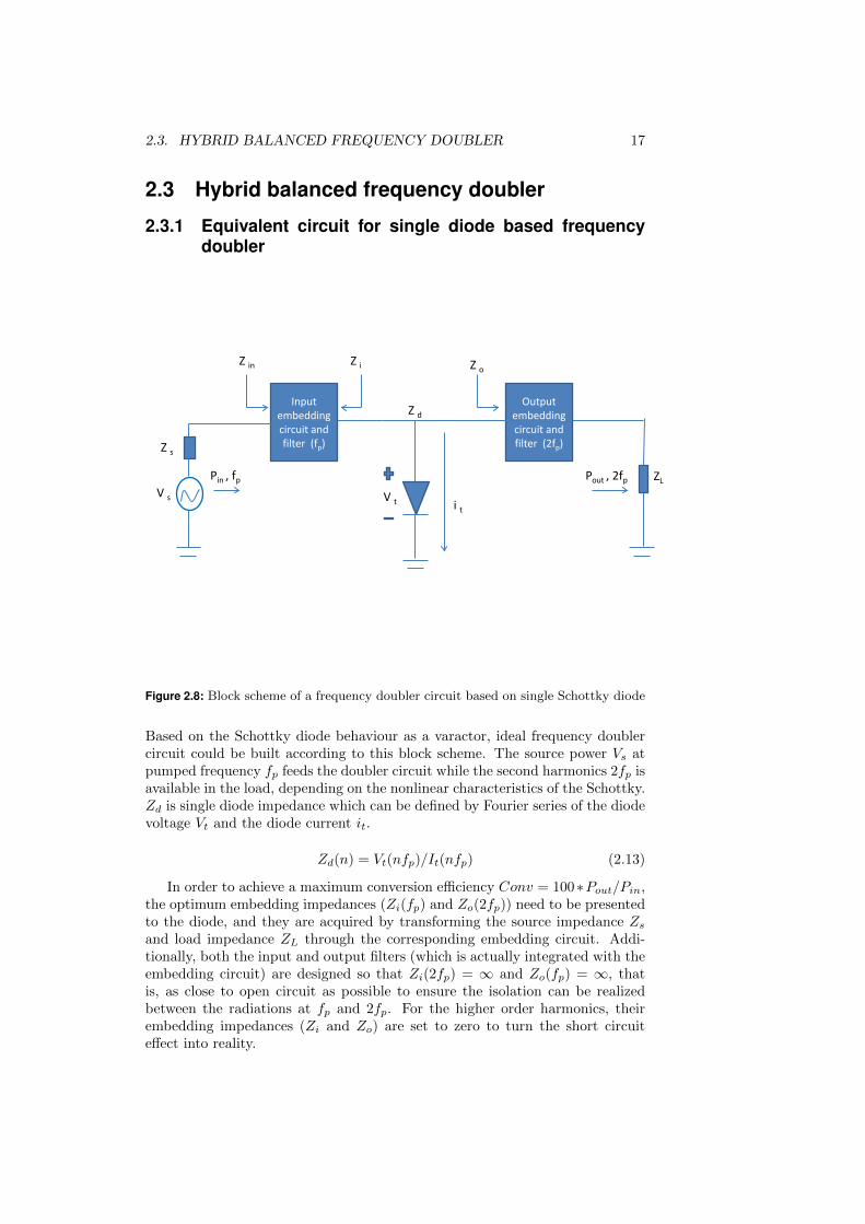
Figure 2.8: Block scheme of a frequency doubler circuit based on single Schottky diode
Based on the Schottky diode behaviour as a varactor, ideal frequency doublercircuit could be built according to this block scheme. The source power Vs atpumped frequency fp feeds the doubler circuit while the second harmonics 2fp isavailable in the load, depending on the nonlinear characteristics of the Schottky.Zd is single diode impedance which can be defined by Fourier series of the diodevoltage Vt and the diode current it.
Zd(n) = Vt(nfp)/It(nfp) (2.13)
In order to achieve a maximum conversion efficiency Conv = 100∗Pout/Pin,the optimum embedding impedances (Zi(fp) and Zo(2fp)) need to be presentedto the diode, and they are acquired by transforming the source impedance Zs
and load impedance ZL through the corresponding embedding circuit. Addi-tionally, both the input and output filters (which is actually integrated with theembedding circuit) are designed so that Zi(2fp) = ∞ and Zo(fp) = ∞, thatis, as close to open circuit as possible to ensure the isolation can be realizedbetween the radiations at fp and 2fp. For the higher order harmonics, theirembedding impedances (Zi and Zo) are set to zero to turn the short circuiteffect into reality.
18 CHAPTER 2. THEORY
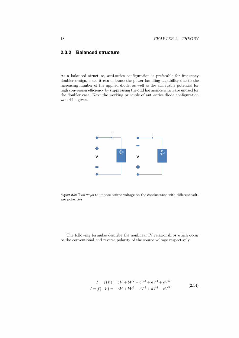
2.3.2 Balanced structure
As a balanced structure, anti-series configuration is preferable for frequencydoubler design, since it can enhance the power handling capability due to theincreasing number of the applied diode, as well as the achievable potential forhigh conversion efficiency by suppressing the odd harmonics which are unused forthe doubler case. Next the working principle of anti-series diode configurationwould be given.
V V
I I
Figure 2.9: Two ways to impose source voltage on the conductance with different volt-age polarities
The following formulas describe the nonlinear IV relationships which occurto the conventional and reverse polarity of the source voltage respectively.
I = f(V ) = aV + bV 2 + cV 3 + dV 4 + eV 5
I = f(−V ) = −aV + bV 2 − cV 3 + dV 4 − eV 5(2.14)
2.3. HYBRID BALANCED FREQUENCY DOUBLER 19
A
V(Zs)
V(s)
V(s)
ZsV(Zs)
Zl
V(Zl)
Zs
B
i(o)
i(o)
i(e)
i(e)i(L)
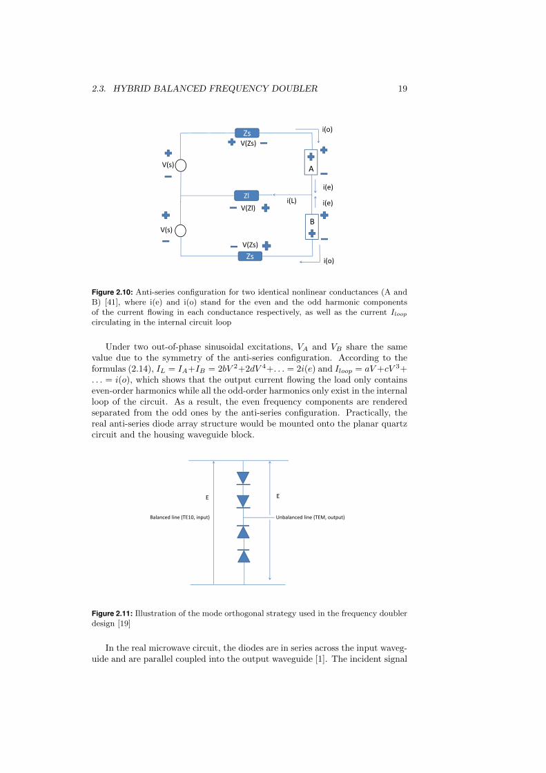
Figure 2.10: Anti-series configuration for two identical nonlinear conductances (A andB) [41], where i(e) and i(o) stand for the even and the odd harmonic componentsof the current flowing in each conductance respectively, as well as the current Iloopcirculating in the internal circuit loop
Under two out-of-phase sinusoidal excitations, VA and VB share the samevalue due to the symmetry of the anti-series configuration. According to theformulas (2.14), IL = IA+IB = 2bV 2+2dV 4+. . . = 2i(e) and Iloop = aV +cV 3+. . . = i(o), which shows that the output current flowing the load only containseven-order harmonics while all the odd-order harmonics only exist in the internalloop of the circuit. As a result, the even frequency components are renderedseparated from the odd ones by the anti-series configuration. Practically, thereal anti-series diode array structure would be mounted onto the planar quartzcircuit and the housing waveguide block.
E E
Balanced line (TE10, input) Unbalanced line (TEM, output)
Figure 2.11: Illustration of the mode orthogonal strategy used in the frequency doublerdesign [19]
In the real microwave circuit, the diodes are in series across the input waveg-uide and are parallel coupled into the output waveguide [1]. The incident signal
20 CHAPTER 2. THEORY
would feed the anti-series diode array in a balanced mode (TE10) which is domi-nant mode in the input rectangular waveguide. By contrary, the excited secondharmonics would propagate along the suspended microstrip line in an unbal-anced mode (TEM). Accordingly, effective isolation between the input and theoutput radiations can be achieved due to the mode orthogonal.
2.3.3 Implementation
Input port (WR-10)
Output port (WR-5)
Varactor chip
Bias port
Transition port (100 Ohm transmission line)
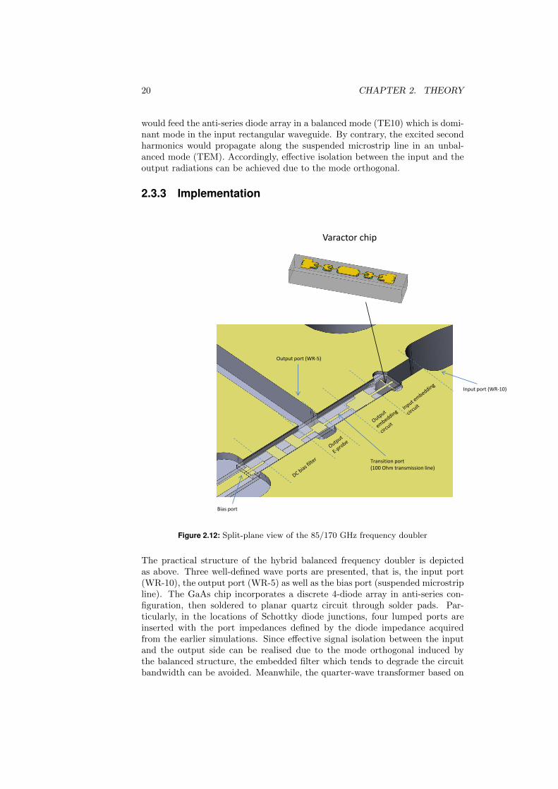
Figure 2.12: Split-plane view of the 85/170 GHz frequency doubler
The practical structure of the hybrid balanced frequency doubler is depictedas above. Three well-defined wave ports are presented, that is, the input port(WR-10), the output port (WR-5) as well as the bias port (suspended microstripline). The GaAs chip incorporates a discrete 4-diode array in anti-series con-figuration, then soldered to planar quartz circuit through solder pads. Par-ticularly, in the locations of Schottky diode junctions, four lumped ports areinserted with the port impedances defined by the diode impedance acquiredfrom the earlier simulations. Since effective signal isolation between the inputand the output side can be realised due to the mode orthogonal induced bythe balanced structure, the embedded filter which tends to degrade the circuitbandwidth can be avoided. Meanwhile, the quarter-wave transformer based on

2.3. HYBRID BALANCED FREQUENCY DOUBLER 21
the reduced-height waveguide is the main body of the input embedding circuit,while the suspended microstrip transmission lines with varying characteristicimpedances are inserted to construct the output embedding circuit, aimed forcoupling the excited second harmonics to the output E-probe. In conjunctionwith a fixed output frequency back-short and a DC bias filter, E-probe can guidethe incident second harmonics to the output waveguide (WR-5). Moreover, theDC bias voltage can feed each Schottky diode though the suspended microstripmetalization.
Input waveguide (WR‐10)
Input embedded circuit
Varactor chip
Output embedded circuit
Output coupler
DC bias filter
Output waveguide (WR‐5)
TEM wave (170 GHz) TE10 wave (85 GHz)
TE10 wave (170 GHz)
Harmonics generation
DC bias voltage
Output
Figure 2.13: Illustration of the functional partition and signal flow of the 85/170 GHzfrequency doubler

22 CHAPTER 2. THEORY

Chapter 3
Method
After the relevant theories regarding the doubler operation have been clarified,it comes to the circuit implementation phase which is characterised by interac-tive and iterative usage of two circuit simulation tools, Advanced Design System(ADS) and High Frequency Structure Simulator (HFSS). The system complex-ity of the frequency doubler escalates from an ideal balanced circuit model inADS to a comprehensive hybrid structure model in HFSS. During the optimi-sation process, more priorities are put to realise a broadband design while theconversion efficiency has to be compromised to some extent. Finally, harmonicbalance simulation is launched to evaluate the complete doubler performance,where four Chalmers Schottky diode models are combined with an imported Sparameter file representing the essence of the chip package structure, the doublercircuits and the waveguide interface.
23

24 CHAPTER 3. METHOD
3.1 Design flow
ADS simulation for ideal single diode based frequency doubler
ADS for ideal balanced frequency doubler
Diode impedance at frequency fp and 2fp
HFSS Modeling of hybrid balanced frequency doubler
Design partition
Input section design Output section design Output coupling arrangement
HFSS simulation for integrated system
Generalized 7-port S-matrix file
Complete harmonic balance simulation in ADS, based on the imported 7-port S file and Chalmers Schottky diode model
Optimum bias voltage and pump power
If not satisfactorying
Checking the conversion efficiency, output power and 3-dB bandwidth
Figure 3.1: Design flow of the 85/170 GHz frequency doubler
The design process of the hybrid balanced frequency doubler, is characterizedby the interactive and iterative usage between Advanced Design System (ADS)based on the harmonic balance technology for nonlinear circuit analysis andHigh Frequency Structure Simulator (HFSS) offering the linear electromagneticsolution to the specified physical structure based on the finite element analy-sis [42]. Initially, the harmonic balance simulation for single diode based fre-quency doubler was carried out in ADS, so as to enable us to be familiar with allkinds of circuit setup for nonlinear analysis. Then, a balanced (anti-series) struc-ture of diode array consisting of four Chalmers Schottky diode model, is used toreplace the single diode structure for enhancing the power handling capabilityand suppressing all the unused odd harmonics. Subsequently, the harmonic bal-ance simulation is carried out to find out the single diode impedance at fp and2fp. Next, the real structure of the GaAs Schottky varactor chip based on thebalanced structure simulated above, is drawn in AutoCAD and then importedto HFSS in conjunction with the specified physical structures of the embeddingand coupling circuits. Aiming to ease the requirements for the computer mem-ory during HFSS simulation, the whole doubler structure is divided into three

3.1. DESIGN FLOW 25
functional parts which can be solved individually, that is, the input section, theoutput section and the output coupling arrangement. A large amount of ge-ometry perturbation for the sub-functional parts is analyzed and hence all thecritical physical dimensions are optimised and updated, considering the trade-offbetween conversion efficiency and 3-dB bandwidth. Finally all the functionalparts are integrated in HFSS for a complete linear electromagnetic structuresimulation. As a consequence, the generalized 7-port S-matrix file with thewell-defined wave ports and lumped ports is imported to ADS, combined withfour Chalmers Schottky diode models connected to the lumped ports. Harmonicbalance analysis is launched to evaluate the simulated performance of the full-structure hybrid balanced frequency doubler. If the simulation results were notsatisfying, the doubler structure in HFSS should be re-optimised to fulfil thedesign specification.
HFSS simulation for the input section at pump frequency, with the de-embedding process to the varactor chip terminal
Symmetry plane (E-wall)
Generalized 4-port S-matrix file
Optimisation process for the input section in ADS
Updated design parameters (location of the input back-short, length of the reduced-height waveguide and etc.)
HFSS simulation for the complete input section structure, checking the return loss of the input port
If not satisfactorying
Figure 3.2: Design flow of the input section of the 85/170 GHz frequency doubler

26 CHAPTER 3. METHOD
HFSS simulation of the output section at the second harmonics, with the de-embedding process to the varactor chip terminal
Symmetry plane (H-wall)
Generalized 3-port S-matrix file
Optimisation process for the output section in ADS
HFSS simulation for the complete output section structure, checking the return loss of the transition port (100 Ohm transmission line)
If not satisfactorying
Updated design parameters (the length and the impedance of the matching transmission line)
Figure 3.3: Design flow of the output section of the 85/170 GHz frequency doubler
HFSS simulation of the output E-probe at the second harmonics with the de-embedding process to E-probe terminal
Generalized 4-port S-matrix file
Optimisation process for the output coupling arrangement in ADS
If not satisfactorying
HFSS simulation of the DC bias filter
Generalized 2-port S-matrix file
Updated design parameters (location of output back-short, length of connection line between DC bias filter and E-probe, and etc.)
HFSS simulation for the complete output coupling arrangement, checking the power transmisson coefficient from the 100 Ohm transmisson line to the output waveguide
Figure 3.4: Design flow of output coupling arrangement of the 85/170 GHz frequencydoubler
Particularly, the interactive and iterative usage between ADS and HFSSsimulator also took place during the partition design phase. As for certain sub-functional part, the preliminary HFSS simulations are responsible for generatingthe generalized S-matrix files, which enclosed the electromagnetic solution to theappointed de-embedding terminals for that part, like the varactor chip termi-nal serving the embedding circuit design, or the E-probe terminal used for the
3.2. SIMULATION SETUP 27
output coupling design. Then the S-matrix files are imported to ADS, com-bined with the ideal device components representing the peripheral structuresin HFSS, where all kinds of critical physical dimensions are involved. Therefore,instead of HFSS simulations which are quite time-consuming, the optimisationprocess for those critical physical dimensions is carried out in ADS effectively,since the direct control could be exerted to the ideal device components andquick circuit responses are achievable. After the optimisation process had beendone in ADS, the critical physical dimensions belonging to the sub-functionalstructure are updated in HFSS and the linear electromagnetic structure simu-lation is launched to evaluate the relevant performance. Iterative process tookplace here in the sense that the operation of the de-embedding and S-file importwould be carried out again for the re-optimisation process in ADS, if the circuitperformance in HFSS had still deviated from our expectations. Additionally,the symmetry plane is fully utilized during the embedding circuit design, whichproved effectively reducing the simulation time in HFSS.
3.2 Simulation setup
3.2.1 Single diode based frequency doubler
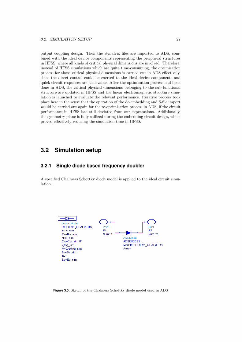
A specified Chalmers Schottky diode model is applied to the ideal circuit simu-lation.
Figure 3.5: Sketch of the Chalmers Schottky diode model used in ADS

28 CHAPTER 3. METHOD
Diode junction area per anode(µm2) 20Doping of epitaxial layer (cm−3) 2× 10¹⁷
Doping of buffer layer (cm−3) 5× 10¹⁸
Thickness of epitaxial layer (µm) 0.27Thickness of buffer layer (µm) 2
Electron mobility of epitaxial layer (cm2/V − s) 3900Electron mobility of buffer layer (cm2/V − s) 1830
Energy gap (eV ) 1.42
Table 3.1: Fixed design parameters of Chalmers Schottky diode model
Reverse saturation current density (A/µm2) 1× 10⁻¹⁵
Parasitic capacitance due to the diode package (fF ) 0Forward conduction barrier potential (V ) 1
Series resistance (Ω) 4
Table 3.2: Adjustable design parameters of Chalmers Schottky diode model, as well astheir initial values
There are some flexible prime parameters which can be tuned to facilitatean agreement between the simulation and measurement. In order to verify thisdiode model, curve fittings are made in terms of IV and CV characterisation, be-tween the real Schottky diode fabricated for measurement use and the ChalmersSchottky diode model for circuit simulation in ADS.
V_DCSRC1Vdc=vb V
diode_varX1
21
DCDC1
DC
ParamSweepSweep1
Step=0.1Stop=1Start=-10SimInstanceName[6]=SimInstanceName[5]=SimInstanceName[4]=SimInstanceName[3]=SimInstanceName[2]=SimInstanceName[1]="DC1"SweepVar="vb"
PARAMETER SWEEP
Figure 3.6: Circuit setup of DC simulation for single Schottky diode in ADS (The em-pirical formulas do not show up here which are used to calculate the CV characteristiccurve for single diode model)

3.2. SIMULATION SETUP 29
Figure 3.7: IV and CV curve fitting between the real Schottky diode and the ChalmersSchottky diode model with the diode junction area of 15 µm2
The curve fittings for the diode IV and CV characteristic are made in dif-ferent ranges of applied DC bias voltage, that is, the forward conduction regionfor the former case and the reverse bias region for the latter thing. For somereasons, the comparison is made with the junction area of 15 µm2 rather thanthe appointed junction area of 20 µm2. For the CV characteristic, the curvefitting can be available by adjusting the diode parasitic capacitance and theforward barrier potential which are applied to the circuit setup, while the seriesresistance and the reverse saturation current density played a dominant role indetermining the IV characteristic. As a result, strong curve fittings are avail-able for both IV and CV characteristic and hence the Chalmers Schottky diodemodel proved reliable enough to be put into use. Since this kind of diode modelis scalable with the diode junction area, the fitting results are also adaptable tothe other area cases.

30 CHAPTER 3. METHOD
vout
diode_varX1
21
I_Probeiout
DC_FeedDC_Feed1
V_DCSRC1Vdc=vb V
P_1TonePORT1
Freq=freq_inP=polar(p_in,0)Z=z_port OhmNum=1
DC_BlockDC_Block1
Figure 3.8: Schematic of the circuit simulation setup in ADS for the 85/170 frequencydoubler based on single Schottky diode (just warm-up, not useful for the followingcircuit designs)
In this circuit setup, both the input and output termination are merged intothe pump source and the diode embedding impedance can be specified directly.On the other hand, the DC path is differentiated from the RF path by addingthe ”DC Block” and the ”DC Feed”. Particularly a pump power at 1 mW ispushed into the Schottky diode such that the bias voltage can be excluded fromthe optimising parameter list. Therefore, only the diode embedding impedancesare left to determine the circuit performance.

3.2. SIMULATION SETUP 31
3.2.2 Balanced Frequency Doubler
Pumped power
Pumped power(out of phase)
Vbias
Vbias
DC path
DC path
load itotal
ibranch
Figure 3.9: Schematic and illustration diagram of the circuit setup of ADS harmonicbalance simulation for the 85/170 GHz frequency doubler in an anti-series configurationof diode array
Anti-series structure is composed of upper and lower meshes pumped with out-of-phase power source. In the figure (3.9), DC path can be explicitly specified bytwo ”DC Block” which are placed next to the power source in case that the biasDC voltage ruins the RF source, and a pair of ”DC feed” in each mesh which areused to isolate the DC voltage source from the RF signal and create DC groundas well. Furthermore, in order to enhance the power handling capability, twodiodes in series connection are applied in each mesh, which can be consideredas an equivalent single Schottky diode but twice the reverse breakdown voltage.Finally the generated power at the second harmonics is supposed to be absorbedby the load as much as possible.

32 CHAPTER 3. METHOD
100 200 300 400 500 600 700 8000 900
0.005
0.010
0.015
0.020
0.025
0.030
0.035
0.040
0.000
0.045
freq, GHz
Mag
nitu
de o
f the
toto
al c
urre
nt (A
)
m2
m2freq=mag(iout.i)=0.042
170.0GHz
100 200 300 400 500 600 700 8000 900
0.005
0.010
0.015
0.020
0.025
0.030
0.000
0.035
freq, GHz
Mag
nitu
de o
f the
bra
nch
curr
ent (
A)
m3
m3freq=mag(iout_b.i)=0.021
170.0GHz
Figure 3.10: Power spectrum of the total current itotal and the branch current ibranch
By the comparison of the two power spectrum shown above, the main ad-vantage of the anti-series configuration is visualized that the suppression of theundesired odd harmonics takes effect in the load, while the magnitude of thesecond harmonic component can be doubled.
3.2.3 Hybrid Frequency Doubler
Thickness of GaAs substrate (µm) 50Thickness of the perfect center conductor (µm) 2
Thickness of the quartz substrate (µm) 100
Table 3.3: Material thickness used in the HFSS modelling

3.2. SIMULATION SETUP 33
Input back‐short
L2
L1
Reduced‐height waveguide
Input port (WR‐10)
Figure 3.11: Structure of the input section for the 85/170 GHz frequency doubler
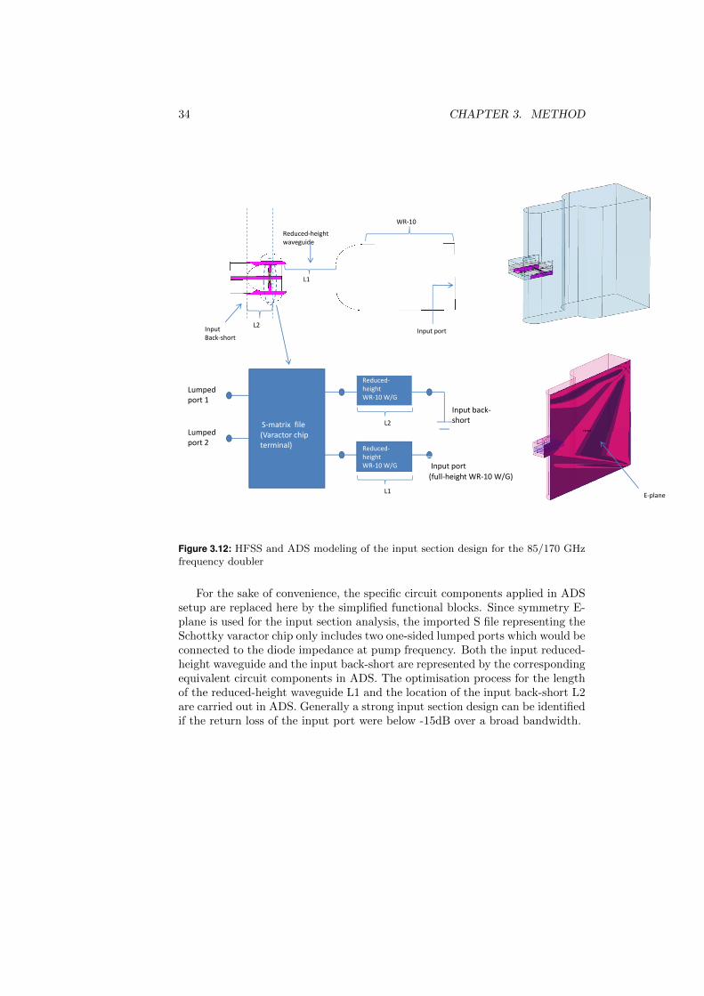
As is depicted in this structure, the input port of the whole doubler systemis provided by the full-height input waveguide (WR-10). Then a quarter-wavetransform strategy based on the input reduced-height waveguide is applied toform the input embedding circuit, in conjunction with an effective input back-short. At the pump frequency TE10 is the only wave mode allowed to propagatein the input waveguide, while the effective input back short would turn the TE10into a evanescent mode due to the enlarged cut-off frequency in the followingreduced-width waveguide channel. As a result, Zi(fp) and Zo(fp) in the figure(2.8) are respectively well-defined by the input embedding circuit and the ef-fective input back-short. Generally the length of the reduced-height waveguide(L1) and the location of the input back-short (L2) are optimised to achievea small return loss in the input port, along with an utilisation of symmetryE-plane for the input section.
34 CHAPTER 3. METHOD
WR‐10
Reduced‐height waveguide
Input Back‐short
Input portL2
L1
Reduced‐height WR‐10 W/G
S‐matrix file (Varactor chip terminal)
Lumped port 1
Lumped port 2
Reduced‐height WR‐10 W/G
Input back‐short
Input port (full‐height WR‐10 W/G)
E‐plane L1
L2
Figure 3.12: HFSS and ADS modeling of the input section design for the 85/170 GHzfrequency doubler
For the sake of convenience, the specific circuit components applied in ADSsetup are replaced here by the simplified functional blocks. Since symmetry E-plane is used for the input section analysis, the imported S file representing theSchottky varactor chip only includes two one-sided lumped ports which would beconnected to the diode impedance at pump frequency. Both the input reduced-height waveguide and the input back-short are represented by the correspondingequivalent circuit components in ADS. The optimisation process for the lengthof the reduced-height waveguide L1 and the location of the input back-short L2are carried out in ADS. Generally a strong input section design can be identifiedif the return loss of the input port were below -15dB over a broad bandwidth.
3.2. SIMULATION SETUP 35
Output frequency back‐short
Transition port (100 Ohm)
Figure 3.13: Structure of the output section for the 85/170 GHz frequency doubler
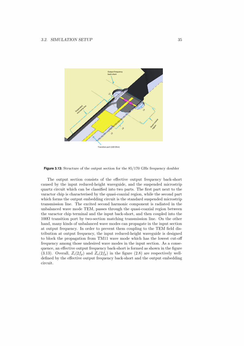
The output section consists of the effective output frequency back-shortcaused by the input reduced-height waveguide, and the suspended microstripquartz circuit which can be classified into two parts. The first part next to thevaractor chip is characterised by the quasi-coaxial region, while the second partwhich forms the output embedding circuit is the standard suspended microstriptransmission line. The excited second harmonic component is radiated in theunbalanced wave mode TEM, passes through the quasi-coaxial region betweenthe varactor chip terminal and the input back-short, and then coupled into the100Ω transition port by two-section matching transmission line. On the otherhand, many kinds of unbalanced wave modes can propagate in the input sectionat output frequency. In order to prevent them coupling to the TEM field dis-tribution at output frequency, the input reduced-height waveguide is designedto block the propagation from TM11 wave mode which has the lowest cut-offfrequency among those undesired wave modes in the input section. As a conse-quence, an effective output frequency back-short is formed as shown in the figure(3.13). Overall, Zi(2fp) and Zo(2fp) in the figure (2.8) are respectively well-defined by the effective output frequency back-short and the output embeddingcircuit.

36 CHAPTER 3. METHOD
Suspended microstripline 1
S‐matrix file (Varactor chip terminal)
Lumped port 1
Lumped port 2
Transition port
Suspended microstripline 2
Reduced‐height waveguide
L4L5 L2
Quasi‐coaxial region
L3Transition port (100 Ohm) Zv2(2fp)
output frequency back‐short
Symmetry plane
H‐planeL5 L4
Zv(2fp)
Z4Z5
Figure 3.14: HFSS and ADS modeling of the output section design for the 85/170 GHzfrequency doubler
Aiming to synthesize an appropriate impedance of Schottky varactor chip atoutput frequency 2fp, L2 and L3 are optimised through HFSS simulation andthe initial chip impedance Zv(2fp) would be transformed to Zv2(2fp) which canease the output embedding circuit design. Subsequently, the generated S fileincluding the essence of the updated Schottky varactor chip interface would beimported to the ADS equivalent circuit accounting for the output section design.The two section matching transmission line is applied to transform Zv2(2fp) tothe transition port impedance 100 Ω as close as possible, and this matchingcircuit is characterised by the length (L4,L5) and the characteristic impedance(Z4,Z5) of each section, which are mainly optimised in ADS. Additionally, sym-metry H-plane is applied for the output section design and the two lumped portsremaining are connected to the diode impedance at frequency 2fp.

3.2. SIMULATION SETUP 37
w
Strip
Er
t
Dielectric substrate
Grounding planea
b
Figure 3.15: Inverse suspended microstrip structure used in HFSS modelling
Shield inverse suspended microstrip transmission line is used to ease themounting process and relieve the system operating sensitivity to the quartzsubstrate thickness. Its characteristic impedance is directly manipulated byadjusting the width of the centre conductor W. As a consequence, a look-uptable can be built to present the one-to-one correspondence between the centreconductor width and the associated characteristic impedance.
Grounding stubSolderpocket
Solder pad
Figure 3.16: Profile of the structure set-up for soldering
By the solder pads shown above, the balanced GaAs Schottky varactor chipis soldered to the quartz circuit. Then, the assembly process is carried out bymounting the quartz circuit into the E-plane split waveguide cavity. Indeed,each end of the chip grounding stub is merged with the silver epoxy filling inthe solder pocket.

38 CHAPTER 3. METHOD
DC bias filter
Output frequency back‐short
Output waveguide (WR‐5)
E‐probe
Transition port
Figure 3.17: Output coupling arrangement for the 85/170 GHz frequency doubler
The main body of the output coupling arrangement is E-probe, in conjunc-tion with a DC bias filter, output back-short and an output reduced-heightwaveguide. Generally the output coupling arrangement serves to couple theradiated power at output frequency of 2fp from the suspended microstrip trans-mission line (100 Ω) to the output waveguide (WR-5) as much as possible. Thereturn loss of the transition port would be measured to quantify the couplingeffects.

3.2. SIMULATION SETUP 39
L9 L7 L6
L8
L10
Bias port
Output port
Transition port
L13
L12
L11
Reduced‐height WR‐5 W/G
S‐matrix file (E‐probe terminal)
Output back‐short
Reduced‐height WR‐5 W/G
Output portfull‐height WR‐5 W/G
Tunable connection line
S‐matrix file(DC bias filter)Bias port
Transition port
L9L6
L10
Open circuit for the output second harmonics
Figure 3.18: HFSS and ADS modeling of the output coupling arrangement for the85/170 GHz frequency doubler
Quarter-wave transformer based filter design is optimized in HFSS to opencircuit the output second harmonics at left E-probe terminal, depending on thephysical dimensions L9, L11, L12 and L13. Meanwhile, the sizes of E-probeL7 and L8 have been specified prior to importing the S matrix file of E-probeterminal to ADS. Generally, the location of the fixed output back-short L6 andthe length of the output reduced-height waveguide L10 are played around inADS to realize a maximum output power coupling from the transmission lineto the output waveguide.

40 CHAPTER 3. METHOD
Input port
Output port
Bias port
lumped port (diode junction)
Input embedding circuit
Output embedding circuitE-probe
DC bias filter
Figure 3.19: HFSS modeling of the complete structure of the 85/170 GHz frequencydoubler
Finally, all the sub-functional parts of the frequency doubler are integratedin HFSS based on the specified structure shown above. After the linear electro-magnetic structure simulation had been done, the generated S matrix file withthree wave ports (input, output and bias) and four lumped ports inserted to thelocation of Schottky diode junction, is imported to ADS so that the nonlinearharmonic balance analysis for the complete doubler structure could be carriedout in such a way

3.2. SIMULATION SETUP 41
S-matrix file
Pump Power
LoadBias port termination
Figure 3.20: Functional diagram of ADS harmonic balance simulation for the completestructure of the 85/170 GHz frequency doubler
It is noted that the bias port is rendered obsolete and terminated with amatching load, since the imported S matrix file had not included the DC so-lution. Therefore, Schottky diode is still individually biased by the specifiedDC voltage source (3.2 V). On the other hand, the source impedance and loadimpedance are set to be equal to the characteristic impedances of the inputwaveguide (WR-10) and output waveguide (WR-5) respectively.

42 CHAPTER 3. METHOD

Chapter 4
Results
In this chapter, both the large signal simulation results from the harmonic bal-ance analysis and the realistic measurement results, are presented and comparedto characterise the fabricated frequency doubler. By exploring the underlyingcauses for the discrepancies between them, the limitations of the hybrid ap-proach are gradually revealed.
43

44 CHAPTER 4. RESULTS
4.1 Simulation results
4.1.1 Contour plot analysis for the ideal balanced frequencydoubler circuit
indep(Z_i) (0.000 to 42.000)
Z_
i
indep(Z_o) (0.000 to 98.000)
Z_
o
2.5 dB
2.5 dB
12.5 dB
12.5 dB
Zin_opt= (24+j137) Ω
Zout_opt= (24+j63) Ω
Figure 4.1: Contour loss contours versus input and output diode embedding impedance,obtained from load-pull harmonic balance simulations in ADS for the ideal 85/170GHz balanced frequency doubler, with a diode junction area of 20 µm2, a bias voltageof 3.5 V for single Schottky diode model and a total pump power of 40 mW. Theminimum conversion loss is 2.5 dB and the contours correspond to 1 dB increment ofthe conversion loss
The efficiency contour plot makes it possible to conduct a trade-off between thediode embedding impedances, the conversion loss and the bandwidth. Appar-ently, the contours show that the conversion efficiency is more sensitive to theinput diode embedding impedance than the output. Furthermore, theoreticallythe minimum conversion loss can be acquired only when the simultaneous con-jugate matching conditions are fulfilled both the input and the output section.In other words, if the optimum diode embedding impedances for the minimumconversion loss have been found in the contour plots, the diode impedancescan be obtained through the conjugate transformation of those optimum diodeembedding impedances. As a result, the diode impedances at pump frequencyZd(fp) and the second harmonic frequency Zd(2fp) are found to be (24-j137) Ωand (24-j63) Ω respectively, which would be used in the HFSS simulation as thelumped port impedance.

4.1. SIMULATION RESULTS 45
4.1.2 Harmonic balance analysis for the complete structureof the hybrid balanced frequency doubler
-8 -7 -6 -5 -4 -3 -2 -1 0-9 1
-40
-30
-20
-10
0
10
20
-50
30
Single diode voltage, V(t) (V)
Sing
le d
iode
cur
rent
, I(t)
(mA)
Phase portrait
Figure 4.2: Simulated output power and conversion efficiency versus pump power forthe 85/170 GHz frequency doubler at the nominal output frequency of 170 GHz witha bias voltage of 3 V for each diode, as well as time domain terminal voltage V(t)versus time domain flowing current I(t) for each diode model with the varying pumppower levels at the nominal output frequency of 170 GHz
Corresponding to a maximum conversion efficiency (21 (%)) at the nominaloutput centre frequency of 170 GHz, the pump power is found at 70 mW alongwith an output power of 15 mW. The diode I(t) vs V(t) characteristic curveshows that during the pumping cycle, the minimum voltage across the diodeterminal is still larger than the reverse breakdown voltage (-9.3 V), even with theoptimum pump power. Therefore, there is still some room for the improvementof the diode operating conditions, so to reach the ”full” drive for each Schottkydiode to achieve the maximum conversion efficiency.

46 CHAPTER 4. RESULTS
Figure 4.3: Simulated output power versus output frequency for the 85/170 GHz fre-quency doubler, with a bias voltage of 3 V for each diode at varying pump powerlevel
According to these simulation results, the frequency doubler turns out to bea broadband design as expected, where two resonances become more and moreobvious when the pump power increases, an the doubler performances at theoutput centre frequency are more or less compromised. With a pump powerof 70 mW, the simulated 3-dB fractional bandwidth is up to 22% with a peakoutput power around 16 mW at the output frequency of 160 GHz and 177 GHzrespectively.

4.1. SIMULATION RESULTS 47
70 75 80 85 90 95 100−12
−10
−8
−6
−4
−2
0
Pump Frequency (GHz)
Inpu
t Ret
urn
Loss
(dB
)
30 mW40 mW50 mW60 mW70 mW80 mW90 mW
Figure 4.4: Simulated input return loss versus output frequency for the 85/170 GHzfrequency doubler with a bias voltage of 3 V for each diode at varying pump powerlevel
In accordance with the previous simulations, the broadband character is alsoverified by the simulated trends of the input return loss of the doubler inputport, especially for a large pump power. However, the simulated values of theinput return loss are quite far away from the expected, which may be one of themain sources limiting the doubler conversion efficiency.
140 150 160 170 180 190 2000
5
10
15
20
25
30
Output Frequency (GHz)
Con
vers
ion
Effi
cien
cy (
%)
2 Ohm4 Ohm6 Ohm
Figure 4.5: Simulated conversion efficiency versus output frequency for the 85/170 GHzfrequency doubler with a pump power of 70 mW, a bias voltage of 3 V for each diodebut varying series resistance
These simulation results prove the theoretical assumption that the con-version efficiency is inversely proportional to the series resistance. However,through the fabrication and mounting process, the real existing series resistancemay deviates from the corresponding empirical value applied to the earlier cir-cuit simulations. Accordingly, a large design uncertainty is inevitably intro-duced.

48 CHAPTER 4. RESULTS
4.2 Measurement Results
Figure 4.6: A scanning electron microscopic photograph showing the Schottky diodegeometry with the anode area of 20 µm2
Figure 4.7: Micrograph of the planar Schottky varactor chip where four diodes areconnected in the anti-series configuration

4.2. MEASUREMENT RESULTS 49
Figure 4.8: Exploded view of the hybrid balanced frequency doubler
Ericsson Power Meter
Frequency Doubler under test
Waveguide Twist
10-dB Directional Coupler IsolatorTaper (WR-8 to WR-10)
ALMA Multiplier
Ericsson Power Meter
Taper (WR-5 to WR-10)
Figure 4.9: Measurement setup for the characterisation of the frequency doubler

50 CHAPTER 4. RESULTS
Agilent E8247C Signal Generator
EricssonEricksonPower Meter
EricssonEricksonPower Meter
EricssonE3631A Triple Output DC Power Supply
ALMA Multiplier
A B
Vbias1
C
Vtune
Vbias2
WR‐8 to WR‐10 Taper
Isolator 10dB Directional Coupler
Waveguide Twist WR‐5 to WR‐10 Taper
Figure 4.10: Illustration of the measurement setup for the characterisation of the fre-quency doubler
Doubler Tripler 2‐stage amp
15 GHz (6 dBm) 30 GHz 90 GHz
Vtune
90 GHz
(Frequency multiplier)
Vtune
0 V
5 V
Vgate
‐0.7 V
0.3 V
Tunable gate voltage for the 2‐stage amplifier (controlled by Vtune )
Figure 4.11: Constitution of the commercial frequency multiplier applied to the sourcesignal generation

4.2. MEASUREMENT RESULTS 51
Combining the Agilent E8247C signal generator with the ALMA W-band water-vapour radiometer active frequency multiplier (×6), an adjustable pump sourcefrom 80 to 90 GHz is available, with a wide tuning range of the pump power from0 to 80 mW (in case of extreme drive). As is shown in figure (4.11), the ALMAfrequency multiplier consists of a frequency doubler, a cascaded frequency triplerand a two-stage power amplifier in the end. The E3631A Triple Output DCPower Supply provides bias voltage Vbias1 to AlMA frequency multiplier for itsnormal operation, while a second bias voltage Vtune feeding the gate terminalof the two-stage amplifier, is used to control the generated pump power out ofthe ALMA frequency multiplier.
After that, an isolator is inserted to minimize the reflected standing wave em-anating from the rest of the measurement setup. Also, a 10-dB directional cou-pler is placed in front of the frequency doubler under test for the measurement ofthe input return loss. Preliminarily the reference point ”A” and ”B” should beconnected directly without the doubler block, and the real pump power Pf canbe captured by the Erickson Power Meter from the through port of directionalcoupler. After reconnecting the frequency doubler, a portion of the reflectedpump power Pcoupling out of the coupling port of the directional coupler canbe read, and the total reflected pump power Preflection can be restored throughthe following mathematic manipulation: Preflection = Pcoupling ∗ 10 + Ploss,where Ploss accounts for the extra loss induced by the waveguide twist which isconsidered integral to the directional coupler.
The frequency doubler is precisely biased by Vbias2 from the remaining unoc-cupied output port of the E3631A Triple Output DC Power supply. Finally, theoutput power P2f of the frequency doubler would be detected by the EricksonPower Meter and associated conversion efficiency can be calculated out. Thefollowing measurement results are used to characterise the fabricated frequencydoubler with a diode junction area per anode of 20 µm2.

52 CHAPTER 4. RESULTS
Figure 4.12: Measured output power and conversion efficiency versus output frequencyfor the 85/170 GHz frequency doubler, with the Vbias2 of -5.3 V and varying pumppower level
It turns out that a peak output power of 7 mW is available at 165 GHzwith a conversion efficiency of 16%. However, the 3-dB bandwidth cannot beextracted from these measurement results since the doubler performances atlower frequency band (below 160 GHz) have been distorted, due to the bandlimitation from the power amplifier being used in the generator system. Ifa broadband power amplifier were available, the doubler performance could bepossible to be retrieved for the missing frequency band. If so, the 3-dB fractionalbandwidth of the doubler is estimated to be 15% for a medium pump power. Onthe other hand, the applied maximum pump power is only 45 mW temporarilydue to the lack of a high power source.

4.2. MEASUREMENT RESULTS 53
Figure 4.13: Curve fitting for both the output power and the conversion efficiency versusthe pump power between the simulation and the measurement, for the 85/170 GHzfrequency doubler at the output frequency of 168 GHz with the Vbias2 of -5.3 V
The measured conversion efficiency turns out to be directly proportionalto the pump power at output frequency of 168 GHz. When the pump powergoes up to 50 mW, the measured conversion efficiency approaches 20% with anoutput power of 10 mW. For a higher pump power, the frequency doubler entersinto the saturation region gradually. Meanwhile, a resultant curve fitting canbe made between the measurement and simulation, by adjusting those tuningprime parameters of the diode model, such as the series resistance, the parasiticcapacitance and the forward conduction barrier potential. Compared to theinitial values which are listed in the table (3.2), the parasitic capacitance, theseries resistance and the forward conduction barrier potential are set to be 13fF, 2 Ω and 0.8 V respectively for achieving an agreement between simulationand measurement. In other words, both the package parasitic capacitance andthe effective diode series resistance prove not being precisely referred during themodelling process.

54 CHAPTER 4. RESULTS
81 82 83 84 85 86 87 88 89 90 91 92−8
−7
−6
−5
−4
−3
−2
−1
0
Pump frequency (GHz)
Inpu
t ret
urn
loss
(dB
)
SimulationMeasurement
Figure 4.14: Comparison of the input return loss versus output frequency between themeasurement and the simulation, where the relevant design parameters of the diodemodel have been updated according to the last simulation (4.13), for the 85/170 GHzfrequency doubler with the Vbias2 of -5.3 V and a pump power of 30 mW
Generally, 1 dB discrepancy on average is found in the input return lossresults between the measurement and simulation. It is partly due to the extracircuit loss existing in the experimental setup. Obviously the measured exces-sive input return loss could be the main factor limiting the doubler conversionefficiency. Therefore, it is speculated that the bottleneck of the doubler systemshould be the input section which is tightly associated with the input returnloss.
Finally, in order to reveal the full power potential of the doubler, someadjustments are done to the existing measurement setup for generating morepump power. One more power amplifier is added to the generator system andthe isolator is removed to facilitate the interaction between the generator andthe frequency doubler under test.

4.2. MEASUREMENT RESULTS 55
Figure 4.15: Measured pump power, output power and conversion efficiency for the85/170 GHz frequency doubler, with the Vbias2 of -5.3 V under the updated measure-ment setup
Under the safe drive level for the power amplifiers, the frequency doublercan handle at least 70 mW of pump power, with a corresponding output powerof 14 mW and conversion efficiency of 17%. Although this measurement resulttends to reflect more things about the essence of the whole integrated systemrather than the pure characterisation of the doubler itself, it can still offer theprofile of the power handling capability of the frequency doubler. Furthermore,an excessive doubler output level of 20 mW is also observed when pushing thepower amplifiers into compression.

56 CHAPTER 4. RESULTS

Chapter 5
Conclusion
Although the expected broadband output of the frequency doubler cannot befully presented due to the restrictions of the realistic experimental setup, anestimated 3-dB fractional bandwidth of 20% is still given under a medium pumppower. In order to explore the full power potential of the doubler under test,some adjustments are done to the initial measurement setup to boost the pumppower. As a result, the maximum output power the doubler can achieve isobserved to be 20 mW if the power amplifiers is driven to compression region.Generally, both the broadband characteristic and the strong power handlingcapability are roughly achieved by the doubler. On the other hand, as weanticipated, the measured conversion efficiency turns out to be more or lesscompromised for the bandwidth extension. Besides the inherent design strategy,another source limiting the conversion efficiency is the unsuccessful input sectiondesign, which is revealed by the excessive measured input return loss. Givenmore time, there is a strong need to re-optimise the input section combinedwith those solder structures shown in the figure (3.16). Additionally, a furtherthermal analysis should be carried out to evaluate the operational condition ofthe GaAs Schottky varactor chip in the future, especially for high power cases.
Talking of the discrepancies between simulations and measurements, one ofmain causes is the diverse measurement environments which introduces vari-eties of extra circuit loss. Furthermore, the solder pads required by the hybridapproach, could bring in some extra parasitic capacitance and extra series resis-tance which aggravate the deviations between the chip 3D package modelling inHFSS and the real fabricated chip structure. Therefore, the harmonic balancesimulation results fail to fully reflect the essence of the doubler. In spite ofthat, rough performance agreements between the measurement and the simu-lation, are still achievable at certain output frequency, by fitting the parasiticcapacitance and the series resistance into the practical values as close as possi-ble, through harmonic balance simulations. Moreover, another source of designuncertainty arising from the hybrid approach is the varying length of the chipgrounding stub shown in the figure (3.16). During the assembly process, theconductive silver epoxy filling in the solder pocket is likely to cause perturba-tion to the length of the grounding stub, which is a critical circuit parametersin terms of sensitivity.
To cope with those kinds of design uncertainty sources induced by the hy-brid approach, more sensitivity analysis of the doubler operating condition have
57

58 CHAPTER 5. CONCLUSION
to be implemented prior to the fabrication stage, so as to ensure the currentdesign is robust enough to afford those design parameter perturbations in theassembly process. Meanwhile, developments of more subtle modelling for thoseengineering uncertainty sources, are worth the efforts to bridge the gap be-tween the simulation and the measurement. Nevertheless, with the operatingfrequency increasing, it becomes a more and more severe task to compensate forthe limitations of the hybrid approach, since any associated design uncertaintyis supposed to exert more negative influence on the measurement performancesonce the doubler circuit dimension shrinks. Alternatively, a monolithic approach(MMIC) is more suitable for the frequency doubler design at several hundredGHz because the tedious assembly process can be avoided. Accordingly, diversesources of design uncertainty should be eliminated effectively and more reliablesimulation results can be obtained to estimate the realistic doubler performanceprecisely. Until now, Schottky diode based frequency doublers have been re-ported to manage to operate up to 800 GHz [43], with a fixed-tuned broadbandand an output power large enough to pump mixers of various kinds.
References
[1] N. Erickson, “High efficiency submillimeter frequency multipliers,” in 1990IEEE MTT-S International Microwave Symposium Digest, May 1990, pp.1301–1304 vol.3.
[2] P. Siegel, “Terahertz technology,” IEEE Transactions on Microwave Theoryand Techniques, vol. 50, no. 3, pp. 910–928, Mar. 2002.
[3] G. Gallerano and S. Biedron, “Overview of terahertz radiation sources,” inFEL Conference, February 2004, pp. 216–221.
[4] P. Siegel, “THz instruments for space,” IEEE Transactions on Antennasand Propagation, vol. 55, no. 11, pp. 2957–2965, 2007.
[5] A. Raisanen, “Frequency multipliers for millimeter and submillimeter wave-lengths,” Proceedings of the IEEE, vol. 80, no. 11, pp. 1842–1852, Nov.1992.
[6] J. R. Thorpe, J. Fletcher, J. M. Chamberlain, R. E. Miles, J. Spencer,E. Huq, M. Oldfield, and C. Mann, “Developments towards the realizationof submillimeter-wave reflex klystron,” in the 9th International Conferenceon Terahertz Electronics, October 2001.
[7] J. H. Booske, W. J. Lee, S. Gallagher, D. v. d. Weide, and C. L. Kory, “Mi-crofabricated TWTs as high power, wideband sources of THz radiation,” inThe 9th International Conference on Terahertz Electronics, October 2001.
[8] R. Blundell, D. C. Papa, E. R. Brown, and C. D. Parker, “Resonant tun-neling diode as an alternative LO for SIS receiver applications,” ElectronicsLetters, vol. 29, pp. 288–290, 1993.
[9] G. Haddad and R. Trew, “Microwave solid-state active devices,” IEEETransactions on Microwave Theory and Techniques, vol. 50, no. 3, pp.760–779, Mar. 2002.
[10] H. Ito, T. Furuta, F. Nakajima, K. Yoshino, and T. Ishibashi, “Photonicgeneration of continuous THz wave using uni-traveling-carrier photodiode,”Journal of Lightwave Technology, vol. 23, no. 12, pp. 4016–4021, 2005.
[11] T. Bryllert, J. Vukusic, A. O. Olsen, and J. Stake, “A broadband het-erostructure barrier varactor tripler source,” in 2010 IEEE MTT-S Inter-national Microwave Symposium Digest, May 2010, p. 1.
59

60 REFERENCES
[12] J. Vukusic, T. Bryllert, T. Emadi, M. Sadeghi, and J. Stake, “A 0.2-W het-erostructure barrier varactor frequency tripler at 113 GHz,” IEEE ElectronDevice Letters, vol. 28, no. 5, pp. 340–342, May 2007.
[13] S. Hollung, J. Stake, L. Dillner, M. Ingvarson, and E. Kollberg, “A dis-tributed heterostructure barrier varactor frequency tripler,” IEEE Mi-crowave and Guided Wave Letters, vol. 10, no. 1, pp. 24–26, Jan. 2000.
[14] T. David, S. Arscott, J.-M. Munier, T. Akalin, P. Mounaix, G. Beaudin,and D. Lippens, “Monolithic integrated circuits incorporating InP-basedheterostructure barrier varactors,” IEEE Microwave and Wireless Compo-nents Letters, vol. 12, no. 8, pp. 281–283, Aug. 2002.
[15] J. Stake, C. Mann, L. Dillner, M. Ingvarson, S. H. Jones, S. Hollung, H. Mo-hamed, B. Alderman, M. Chamberlain, and E. Kollberg, “Improved diodegeometry for planar heterostructure barrier varactors,” in The 10th Inter-national Symposium on Space Terahertz Technology, 1999, pp. 485–491.
[16] M. Saglam, B. Schumann, K. Duwe, C. Domoto, A. Megej, M. Rodriguez-Girones, J. Muller, R. Judaschke, and H. Hartnagel, “High-performance450-GHz GaAs-based heterostructure barrier varactor tripler,” IEEE Elec-tron Device Letters, vol. 24, no. 3, pp. 138–140, 2003.
[17] Q. Xiao, J. Hesler, T. Crowe, I. Weikle, R.M., Y. Duan, and B. Deaver,“High-efficiency heterostructure-barrier-varactor frequency triplers usingAlN substrates,” in 2005 IEEE MTT-S International Microwave Sympo-sium Digest, 2005, p. 4 pp.
[18] J. Hacker, A. Sailer, B. Brar, G. Nagy, R. Pierson, and J. Higgins, “Ahigh-power W-band quasi-optical frequency tripler,” in 2003 IEEE MTT-SInternational Microwave Symposium Digest, vol. 3, 2003, pp. 1859–1862vol.3.
[19] D. Porterfield, T. Crowe, R. Bradley, and N. Erickson, “A high-power fixed-tuned millimeter-wave balanced frequency doubler,” IEEE Transactions onMicrowave Theory and Techniques, vol. 47, no. 4, pp. 419–425, Apr. 1999.
[20] S. S. Kamaljeet, “Development of frequency multiplier technology forALMA,” ALMA Memo 337.
[21] A. Maestrini, J. Ward, C. Tripon-Canseliet, J. Gill, C. Lee, H. Javadi,G. Chattopadhyay, and I. Mehdi, “In-phase power-combined frequencytriplers at 300 GHz,” IEEE Microwave and Wireless Components Letters,vol. 18, no. 3, pp. 218–220, 2008.
[22] A. Maestrini, J. S. Ward, J. J. Gill, C. Lee, B. Thomas, R. H. Lin, G. Chat-topadhyay, and I. Mehdi, “A frequency-multiplied source with more than1 mW of power across the 840-900 GHz band,” IEEE Transactions onMicrowave Theory and Techniques, vol. 58, no. 7, pp. 1925–1932, 2010.
[23] J. V. Siles and J. Grajal, “Physics-based design and optimization ofSchottky diode frequency multipliers for terahertz applications,” IEEETransactions on Microwave Theory and Techniques, vol. 58, no. 7, pp.1933–1942, 2010.

REFERENCES 61
[24] M. C. Markus Krach, Jrgen Freyer, “An integrated ASV frequency triplerfor millimetre-wave applications,” in 33rd European Microwave Conference,2003.
[25] D. W. Porterfield, “A 200 GHz broadband, fixed-tuned, planar doubler,”in Tenth International Symposium on Space Terahertz Technology, March1999.
[26] B. Thomas, J. Treuttel, D. M. Byron Alderman, and T. Narhi, “Applicationof substrate transfer to a 190 GHz frequency doubler and 380 GHz sub-harmomic mixer using MMIC foundry Schottky diodes,” in Millimeter andSubmillimeter Detectors and Instrumentation for Astronomy IV, 2008.
[27] I. Kallfass, H. Massler, A. Tessmann, A. Leuther, M. Schlechtweg, andG. Weimann, “A broadband frequency sixtupler MIMIC for the W-bandwith > 7 dBm output power and > 6 dB conversion gain,” in 2007IEEE/MTT-S International Microwave Symposium, 2007, pp. 2169–2172.
[28] M. Abbasi, R. Kozhuharov, C. Karnfelt, I. Angelov, I. Kallfass, A. Leuther,and H. Zirath, “Single-chip frequency multiplier chains for millimeter-wavesignal generation,” IEEE Transactions on Microwave Theory and Tech-niques, vol. 57, no. 12, pp. 3134–3142, 2009.
[29] Y. Campos-Roca, C. Schworer, A. Leuther, and M. Seelmann-Eggebert,“G-band metamorphic HEMT-based frequency multipliers,” IEEE Trans-actions on Microwave Theory and Techniques, vol. 54, no. 7, pp. 2983–2992,2006.
[30] V. Radisic, M. Micovic, M. Hu, P. Janke, C. Ngo, L. Nguyen, L. Samoska,and M. Morgan, “164-GHz MMIC HEMT doubler,” IEEE Microwave andWireless Components Letters, vol. 11, no. 6, pp. 241–243, Jun. 2001.
[31] C. Schworer, Y. Campos Roca, A. Leuther, A. Tessmann, M. Seelmann-Eggebert, H. Massler, M. Schlechtweg, and G. Weiman, “A 150 to 220 GHzbalanced doubler MMIC using a 50 nm metamorphic HEMT technology,”in 2005 European Microwave Conference, vol. 3, 2005, p. 4 pp.
[32] “European Schottky technology,” Statement of Work, European SpaceAgency, Issue: 1 Revision: 1 Date: 01.04.2008.
[33] P. Penfield and R. P. Rafuse, Varactor applications. Cambridge: M.I.TPress, 1962.
[34] J. M. Manley and H. E. Rowe, “Some general properties of nonlinear ele-ments,” in IRE Proc, July 1956, pp. 904–913.
[35] R. H. Pantell, “General power relationships for positive and negative non-linear resistive elements,” in IRE Proc, Dec 1958, pp. 1910–1913.
[36] A. Uhlir, “The potential of semiconductor diodes in high frequency com-munications,” in IRE Proc, 1958, pp. 1099–1115.
[37] J. Stake, Varactors, in The RF and Microwave Handbook. CRC Press,2001.

62 REFERENCES
[38] S. A. Maas, Harmonic balance and large-signal-small-signal analysis, inNonlinear Microwave Circuits. Norwood, MA: Artech House, 1988.
[39] C. B. Burckhardt, “Analysis of varactor frequency multipliers for arbitrarycapacitance variation and drive level,” The Bell System technical journal,pp. 675–692, April 1965.
[40] J. C. Marek T. Faber and M. E. Adamski, Microwave and millimeter-wavediode frequency multipliers. Norwood, MA: Artech House, 1995.
[41] S. A. Maas, Harmonic balance and large-signal-small-signal analysis, inNonlinear Microwave and RF Circuits, 2nd ed. Norwood, MA: ArtechHouse, 2003.
[42] G. Gallerano and S. Biedron, “Finite element analysis of a planar diodedoubler,” in Tenth International Symposium on Space Terahertz Technol-ogy, pp. 326–339.
[43] G. Chattopadhyay, E. Schlecht, J. Gill, S. Martin, A. Maestrini, D. Pukala,F. Maiwald, and I. Mehdi, “A broadband 800 GHz Schottky balanced dou-bler,” IEEE Microwave and Wireless Components Letters, vol. 12, no. 4,pp. 117–118, Apr. 2002.