
Low-voltage digitally controlled current differencing buffered ...

Exclusive Technology Feature
© 2020 How2Power. All rights reserved. Page 1 of 16
ISSUE: December 2020
Modeling Digitally Controlled PFCs Made Easy
by Nikhilesh Kamath, ON Semiconductor, Phoenix, Ariz.
The emergence of server farms storing and processing vast amounts of data has spurred interest in highly
efficient and compact hardware infrastructure. Naturally, these requirements extend to the server power supplies. To achieve these objectives, power supply designers need simulations to evaluate tradeoffs in
selecting parameters like inductance, switching frequency, current sense gain etc. while optimizing system
performance metrics like power factor (PF), total harmonic distortion (THD), control loop bandwidth and phase margin.
However, simulation of digitally controlled power supplies has its challenges. For example, it is easy to lose
track of the gain at various points in the system that may occur while converting floating-point compensator
coefficients to fixed-point representation. This article discusses how to address these types of challenges in a specific application of digital control—power factor correction (PFC) circuits. In particular, this article aims to
serve as a guide for designing a digital average-current-mode control scheme, a popular choice for high-power
PFC applications. The techniques and procedures laid out in this article can be extended to voltage-mode control or peak-current-mode architectures as well.
Running simulations typically requires making tradeoffs between run time and accuracy. A smaller simulation
step size yields results that are more accurate but also requires more time for the simulation to complete. This tradeoff is particularly important in the case of power factor correction circuits that are designed with a voltage
loop control bandwidth of less than 10 Hz. Since such systems may take hundreds of milliseconds to reach
steady state during startup and on application of load transients, simulating all operating points may not be feasible. This article discusses the steps involved in modeling a 500-W average-current-mode-controlled PFC
circuit using MATLAB, which features a SPICE-like circuit solver.
A switching model is simulated using power stage components from the Simscape Electrical toolkit. The Simscape toolkit is an extension of the capabilities of the Simulink programming environment and provides a
convenient means to model a physical system (in our case an electrical system). An average model is
developed in the Simulink environment to analyze the system stability. The approach presented here is a
simple, quick and effective means to visualize system behavior. The data handling capabilities of MATLAB software allow for parameterizing simulation models, running from scripts and data logging; important in the
data driven decision-making world we now live in.
Example PFC Requirements For A Server Power Supply
A typical server power supply would have voltage, PF, and efficiency specifications similar to those in Table 1.
Table 1. Example server power supply specifications.[1]
Ac input voltage range 180 to 265 Vac
Ac input frequency 60 Hz (typical)
PF, measured at 230 Vac > 0.97, 30% to 100% of full load
> 0.85, 10% to 30% of full load
THD < 5%, 50% to 100% of full load
< 10%, 20% to 100% of full load
Efficiency, measured at 230 Vac, 60 Hz with fan Peak efficiency > 97%, 30% to 100% of full load
Min. efficiency > 95%, 30% to 100% of full load
Min. efficiency > 92%, 10% to 30% of full load

Exclusive Technology Feature
© 2020 How2Power. All rights reserved. Page 2 of 16
If we look at a typical server power supply design, we then see power supply parameters such as those shown in Table 2, which includes parameters needed for simulation.
Table 2. Simulation system parameters.
Ac input voltage 230 Vac
Ac input frequency 60 Hz
Output voltage 384 V
Output power 500 W
Boost inductor 500 µH
PWM switching frequency 100 kHz
Output capacitance 220 µF
Current sense ratio 0.62
Next, let’s consider the basic structure and control scheme of the circuit we’ll be simulating. Fig. 1 shows a
high-level block diagram of a digitally controlled PFC. An outer voltage loop regulates the output voltage (bulk
voltage) while an inner current loop helps shape the input current by comparing the sensed inductor current with a current reference derived by multiplying the output of the voltage loop with the rectified line voltage.
Fast analog comparators are used for cycle-by-cycle overcurrent protection (OCP). Both voltage and current
loops are analyzed below for various loads because PFC is a front-end converter that can be followed by a
constant power, constant current or constant resistance stage based on the application.
Fig. 1. A simplified overall block diagram of a digitally controlled PFC.
Voltage-Loop Analysis
Ray Ridley developed a small-signal circuit model of the boost power factor circuit[2] in 1987. The current
reference that the inductor current tracks is derived from the line voltage. Ignoring disturbances due to input
voltage, the circuit reduces to the network shown in Fig. 2 and the control-to-output transfer function is given by:

Exclusive Technology Feature
© 2020 How2Power. All rights reserved. Page 3 of 16
(1)
where is the average output voltage, is the average control voltage, ZL is the load impedance, rO is the
small-signal output resistor given by VO/IO, C is the output capacitance, and gC is a constant given by
(VIN)2/(k*VO), where 1/(k) is the line voltage scaling factor.[2]
Fig. 2. A reduced small-signal circuit model of the boost power factor correction circuit.
For a constant-resistance load, ZL = RL, (rO // ZL) = RL/2, the transfer function becomes:
(2)
For a constant-current load, ZL = ∞, (rO // ZL) = rO:
(3)
And finally for a constant-power load, ZL = -VO/IO = -rO, (rO // ZL) = ∞:
(4)
The expressions for IL and gC[2] are given by:
, where M is the conversion ratio given by .
This result can be substituted into equations 2, 3 and 4 to obtain the transfer function from IL to ṼO:
for constant resistance load
for constant current load

Exclusive Technology Feature
© 2020 How2Power. All rights reserved. Page 4 of 16
for constant power load
We can then use these expressions to plot the response of our design example. Table 3 shows the plant transfer
function for our system parameters: C = 220 µF, VIN = 230 Vac, VO = 384 V, RL = 295 Ω and IO = 1.3 A.
Table 3. Plant transfer functions for different load models.
Load model Pole location Bode plot
Constant resistance
4.9 Hz
Constant current
2.45 Hz
Constant power
Origin pole
intersects 0 dB at
434 Hz.

Exclusive Technology Feature
© 2020 How2Power. All rights reserved. Page 5 of 16
With expressions for the plant transfer function in hand, we can begin the process of compensating the voltage loop. Fig. 3 represents the voltage-loop block diagram of the simplified boost converter shown earlier in Fig. 1.
Fig. 3. Voltage-loop block diagram with constant-current plant model.
KVIN represents the external resistor divider gain (160:1 ratio) similar to that of the output voltage KVO (155:1).
(The voltage divider ratio (155 to 160) is commonly used for interfacing a 400-V output to a microcontroller on
a 3.3-V rail.)
A 12-bit SAR ADC senses the line voltage differentially. The analog signal over a range of -3.3 V to 3.3 V is
converted to an integer in the range of 0 to 4096. The effective ADC gain is (4096/6.6).
The gain factor KM is shown to represent any feedforward function or normalization. In this simulation, line
feedforward is not used.
For current sensing, a 10-bit SAR ADC is used and external current-sense gain is 0.62. This gives us the
relationship between the digital current reference (IREF) and inductor current (IL):
For output voltage sensing, a 10-bit SAR ADC is used.
A 2.2-nF capacitor placed on the feedback resistor divider provides a low-pass RC filter for anti-aliasing. This upper resistor in the divider = 4160 kΩ. The lower resistor in the divider = 27 kΩ.
The cut-off frequency is:
= ~2.7 kHz
The feedback voltage is sampled at 10 kHz. This sample rate is sufficient since the target voltage control loop bandwidth is very low (less than 10 Hz).

Exclusive Technology Feature
© 2020 How2Power. All rights reserved. Page 6 of 16
A notch filter can be used to attenuate the 2x line frequency ripple present on the control voltage (output of voltage compensator) or feedback voltage signal. Since the control voltage is used to generate the current
reference for the inner current-loop control, the reference is more accurate, leading to better system
performance (PF, THD).
Reference 6 was consulted to ensure that all components in Fig. 3 were accounted for and that the sample rate
selections for the sense signals were reasonable. Final values (for example, the current-sense gain) were
adjusted based on emulation results.
Fig. 4 shown below is a Simulink model of the voltage-loop block diagram presented in Fig. 3.
Fig. 4. A Simulink model for the voltage loop with a constant-current plant model.
For the constant-resistance model, optimal placement of the compensation zero is at the location of the plant pole.[2] The amount of output capacitance is typically based on the hold-up time requirement. A common rule of
thumb is 0.5 to 1 µF per W.
For a 500-W design, an output capacitance of 440 µF is reasonable. This leads to a compensation zero at 2.5 Hz
in order to cancel the load pole. For this simulation, the selected output capacitance is 220 µF, which corresponds to a load pole at 4.9 Hz for the constant-resistance model and a load pole at 2.45 Hz for the
constant-current load.
The procedure is to plot the plant transfer function, place the compensation zero and adjust the compensator gain to achieve the target crossover frequency.
An S-domain PI compensator with a compensation zero placed at 2.5 Hz and 40 dB gain at 0.1 Hz is described
by the following expression:

Exclusive Technology Feature
© 2020 How2Power. All rights reserved. Page 7 of 16
where the origin pole is given by wp = Ki and wz = Ki/Kp with the following values:
wz = 2*π*2.5 = 15.7 rad/s
wp = 2* π *10 = 62.8 rad/s
In our example, this leads to the following expression for the compensator:
Now, converting to the z-domain using the backward Euler method and a sample rate of 100 µs yields
Comparing to a generic z-domain digital filter with format , the coefficients are:
B0 = 4.00628, B1 = -4, A1 = -1
Divide by 23 to bring the coefficients into the range -1 to +1. Then multiply by 215:
B0 = 4.00628 * 4096 = 16,409.723 = 16410
B1 = -4 * 4096 = -16384
A1 = -1 * 4096 = -4096
The implemented difference equation becomes:
U(n) = U(n-1) + 16410*E(n) – 16384*E(n-1)
and remember to divide by 212.
Alternately,
]
where Kpz = 16384, Kiz = 26 and div. = 4096.

Exclusive Technology Feature
© 2020 How2Power. All rights reserved. Page 8 of 16
Table 4 shows the PI compensator coefficients for the compensator example given above along with the coefficients obtained for other compensator values. The response obtained for case (b) is plotted in Fig. 5, while
Fig 6 shows the PI coefficients plugged into a block diagram for the compensator.
Table 5 depicts what the compensation coefficients in cases (b) and (c) (and a variation on case (c)) mean in terms of loop bandwidth and stability under the different load models. These illustrate tradeoffs in loop
response and stability.
Table 4. A few different voltage compensators with different zero locations and dc gain.
Backward Euler transformation, Ts
= 100 µs
Zero location
(Hz)
Gain at 0.1 Hz
(dB)
Gain at 100 Hz
(dB)
(a) Kpz = 16384, Kiz = 26, divide = 4096
2.52 40 12.1
(b) Kpz = 600, Kiz = 1, divide = 256 2.65 35.8 7.41
(c) Kpz = 800, Kiz = 1, divide = 128 1.99 41.9 15.9
Fig. 5. Voltage-loop PI compensator Bode plot for case (b), overall Bode (with 180-Vac input and
the constant-current load model).
Fig. 6. Voltage-loop compensator for case (b).

Exclusive Technology Feature
© 2020 How2Power. All rights reserved. Page 9 of 16
Table 5. Voltage-loop bandwidth and phase margin for different load models and compensators.
Voltage compensator Crossover frequency and phase margin (PM)
Constant-resistance
model
Constant-current model Constant-power model
180 Vac 230 Vac 180 Vac 230 Vac 180 Vac 230 Vac
Kpz = 600, Kiz = 1,
divide = 256,
IREF div. = 2048
1.7 Hz
(103º PM)
3.25 Hz
(106º PM)
2.9 Hz
(87º PM)
4.65 Hz
(86.7º PM)
3.52 Hz
(52º PM)
5.16 Hz
(61º PM)
Kpz = 800, Kiz = 1, divide = 128,
IREF div. = 4096
1.98 Hz (112º PM)
4.49 Hz (112º PM)
3.51 Hz (94º PM)
5.92 Hz (92º PM)
4.15 Hz (63º PM)
6.4 Hz (70.7º
PM)
Kpz = 800, Kiz = 1,
divide = 128,
IREF div. = 2048
6.12 Hz
(109º PM)
11.3 Hz
(100º PM)
7.34 Hz
(91º PM)
12.1 Hz
(88º PM)
7.73 Hz
(73º PM)
12.3 Hz
(77º PM)
Current-Loop Analysis
A similar approach to that described above can be applied to compensating the current loop. In place of the
voltage-loop diagram from Fig. 3, we have the current-loop diagram shown in Fig. 7.
In this case, the plant transfer function is the load current as a function of duty cycle. From reference 7, we have the following expression for the small-signal duty to inductor current transfer function:
Applying the high-frequency approximation:[7]
, which is also shown in Fig. 7.
Fig. 7. Current-loop block diagram.

Exclusive Technology Feature
© 2020 How2Power. All rights reserved. Page 10 of 16
For our system parameters, L = 500 µH and VO = 384 V, we have:
When a Bode plot of this transfer function is plotted, the magnitude plot intersects 0 dB at ~122 kHz.
As given previously, the current sense gain is 0.62.
A low-pass RC filter is used as an anti-aliasing filter. R = 2 kΩ and C = 400 pF.
The cut-off frequency is:
Current Reference Generation, IREF
The current reference is the product of the output of the voltage control loop (VCONTROL) and instantaneous line
voltage sense (VLINE). The reference current level rises in response to an increased load demand.
For analyzing the dynamics of the current loop, IREF is held constant. It is external to the loop of interest and its
magnitude plays no role.
Digital PWM Gain
The output of the current-loop compensator is stored in a 16-bit compare register. The digital PWM output toggles once the module’s base timer/counter crosses the compare value. The base timer resolution is
determined by the peripheral clock configuration. The PWM clock is set to 192 MHz corresponding to a 5.208-ns
duty cycle resolution. The desired PWM switching frequency is 100 kHz. Hence, a compare register value of 1920 corresponds to 100% duty cycle. In reality, a maximum duty cycle exists, set at ~97%.
The target bandwidth of the current loop is typically around 6 to 10 kHz. The uncompensated Bode plot from
Icomp to Ics digital, pictured in Fig. 8, shows that the loop gain is already close to 0 dB at the target crossover frequency of 10 kHz. So the current compensator need not provide any gain in this region. The compensation
zero can be placed sufficiently low to provide the necessary phase boost at 10 kHz as shown in the Bode plots
on the right in Fig. 8.
Fig. 8. Bode plots of the uncompensated (left) and compensated (right) current loop.
Since the system is first order, a simple PI compensator comprised of a pole at the origin and a zero at a
desired location is suitable. A block diagram of the current-loop compensator is presented in Fig. 9 with coefficients shown for case (c) in Table 6 and the corresponding Bode plots for this compensator design.

Exclusive Technology Feature
© 2020 How2Power. All rights reserved. Page 11 of 16
The current-loop compensator values were derived in a similar manner to that described for the voltage-loop compensator. Table 6 shows the compensator coefficients along with the resulting bandwidth and stability
results obtained for different zero placements. A Simulink model of the current loop is pictured in Fig. 10.
Fig. 9. Current-loop PI compensator and Bode plot.
Fig. 10. Simulink model for the current loop.

Exclusive Technology Feature
© 2020 How2Power. All rights reserved. Page 12 of 16
Table 6. A few current-loop compensators with different zero locations and the resultant bandwidths and phase margins.
Current compensator values with
1/64 post-scale
Backward Euler transformation,
Ts = 10 µs
Zero location
(Hz)
Crossover frequency &
phase margin
Case (a) Kpz = 48, Kiz = 1 328 9.24 kHz, 69°
Case (b) Kpz = 48, Kiz = 4 1270 9.56 kHz, 63°
Case (c) Kpz = 48, Kiz = 8 2440 10.1 kHz, 56°
Case (d) Kpz = 48, Kiz = 12 3500 10.7 kHz, 50°
The final current-loop PI compensator selected is case (c): Kpz = 48 and Kiz = 8 with 1/64 post-scale since it
provides sufficient phase margin while achieving high bandwidth.
Simscape Model
Once the compensators are designed, they are used in the Simscape model shown in Fig. 11 to observe steady-
state waveforms, inductor current ripple, output voltage ripple, transient performance, etc. The filtered line
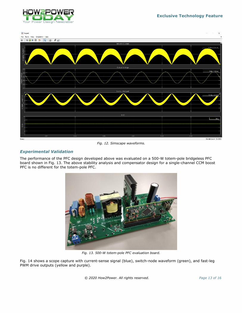
current is passed to the THD block to get a rough measurement of distortion. Fig. 12 shows the simulation waveforms at steady state: inductor current, output voltage, output of the current loop compensator and THD.
Fig. 11. The Simscape model.
Exclusive Technology Feature
© 2020 How2Power. All rights reserved. Page 13 of 16
Fig. 12. Simscape waveforms.
Experimental Validation
The performance of the PFC design developed above was evaluated on a 500-W totem-pole bridgeless PFC
board shown in Fig. 13. The above stability analysis and compensator design for a single-channel CCM boost
PFC is no different for the totem-pole PFC.
Fig. 13. 500-W totem-pole PFC evaluation board.
Fig. 14 shows a scope capture with current-sense signal (blue), switch-node waveform (green), and fast-leg
PWM drive outputs (yellow and purple).

Exclusive Technology Feature
© 2020 How2Power. All rights reserved. Page 14 of 16
Fig. 14. Waveforms obtained from the 500-W totem-pole PFC evaluation board with 180-Vac,
540-W, 60-Hz ac input with PF = 0.995 and THD <3%.
Fig. 15 shows a scope capture with current-sense signal (blue), output voltage (green), slow-leg low-side drive SRLO (yellow) and the output of the voltage-loop compensator (Vcontrol DAC, purple).
Fig. 15. Additional waveforms obtained from the totem-pole PFC evaluation board with Vin = 180
Vac and output power = 500 W.
Fig. 16 compares the expected bandwidth and phase margin from Simulink to actual measurements using a
network analyzer. The plots match quite well.

Exclusive Technology Feature
© 2020 How2Power. All rights reserved. Page 15 of 16
Fig. 16. Bode plot: simulation versus measured results at 180-Vac input and 500-W output using
the constant-current model.
Fig. 17 shows the power factor across load for two different line-voltage levels, 180 Vac and 230 Vac.
Fig. 17. Power factor vs output power.
Conclusion
Simulink and Simscape have been used to analyze an average-current-mode-controlled power factor correction
circuit for a 500-W server power supply application. The selected simulation parameters are validated on a prototype board.
References
1. Open Rack Specification V2.2
2. “Average small-signal analysis of the boost power factor correction circuit” by R.B. Ridley, 1987. (This source provides a PDF preview of the paper when viewed in Internet Explorer.)
3. “Compensating a PFC Stage, TND382-D,” ON Semiconductor presentation.
4. Second-order IIR notch filter, filter model described in MathWorks Help Center.

Exclusive Technology Feature
© 2020 How2Power. All rights reserved. Page 16 of 16
5. “Applying Digital Technology to PWM Control-Loop Designs” by Mark Hagen and Vahid Yousefzadeh, Texas Instruments seminar paper.
6. “Introduction to Digital Control of Switched Mode Power Converters,” seminar delivered by Delta Electronics
to ON Semiconductor, Nov. 2014.
7. “Digital control for power factor correction” by Manjing Xie, Master Thesis, Virginia Tech, 2003
About The Author
Nikhilesh Kamath currently works as a staff applications engineer for the Power Conversion Solutions business unit under the Advanced Solutions Group (ASG) at ON Semiconductor. He
works on product definition, emulation, silicon evaluation and reference design development.
Nikhilesh joined ON Semiconductor in February 2015. Nikhilesh holds a master of science in electrical engineering from North Carolina State University and a bachelor of technology in
electrical and electronics engineering from National Institute of Technology Karnataka, India
For more information on designing power factor correction circuits, see the How2Power’s Design Guide, locate
the Popular Topics category and select “Power Factor Correction”.