Modeling and Characterization of a PFC Converter in the ... and Characterization of a PFC Converter...
124
Modeling and Characterization of a PFC Converter in the Medium and High Frequency Ranges for Predicting the Conducted EMI Liyu Yang Thesis submitted to the Faculty of the Virginia Polytechnic Institute and State University in partial fulfillment of the requirements for the degree of Master of Science in Electrical Engineering APPROVED: F. C. Lee, Co-Chairman W. G. Odendaal, Co-Chairman J. D. van Wyk September 8, 2003 Blacksburg, Virginia Key Words: Modeling and Characterization, PFC converter, Conducted EMI
Transcript of Modeling and Characterization of a PFC Converter in the ... and Characterization of a PFC Converter...

Modeling and Characterization of a PFC Converter in the
Medium and High Frequency Ranges for Predicting the
Conducted EMI
Liyu Yang
Thesis submitted to the Faculty of the
Virginia Polytechnic Institute and State University
in partial fulfillment of the requirements for the degree of
Master of Science
in
Electrical Engineering
APPROVED:
F. C. Lee, Co-Chairman W. G. Odendaal, Co-Chairman
J. D. van Wyk
September 8, 2003
Blacksburg, Virginia
Key Words: Modeling and Characterization, PFC converter, Conducted EMI

Modeling and Characterization of a PFC Converter in the Medium and
High Frequency Ranges for Predicting the Conducted EMI
Abstract
By Liyu Yang
Fred C. Lee, Co-chairman
Willem G. Odendaal, Co-chairman
This thesis presents the conducted electro-magnetic interference (EMI) prediction results
for a continuous conduction mode (CCM) power factor correction (PFC) converter as
well as the theoretical analysis for the noise generation and propagation mechanisms.
In this thesis, multiple modeling and characterization techniques in the medium and high
frequency ranges are developed for the circuit components that are important contributors
to the EMI noise, so that a detailed simulation circuit for EMI prediction can be
constructed.
The conducted EMI noise prediction from the simulation circuit closely matches the
measurement results obtained by a spectrum analyzer. Simulation time step and noise
separator selection are two important issues for the noise simulation and measurement.
These two issues are addressed and the solutions are proposed.
The conducted EMI generation and propagation mechanisms are analyzed in a systematic
way. Two loop models are proposed to explain the EMI noise behavior. The effects of the
PFC inductor, the parasitic capacitance between the device and the heatsink, the
rising/falling time of the MOSFET VDS voltage, and the input wires are studied to verify
the validity of the loop models.

Acknowledgements
iii
Acknowledgements
I would like to express deep and sincere gratitude to those who made this work possible:
professors, friends and family.
For my advisor, Dr. Lee, a previous student says that he is a living legend in the power
electronics community and I would really agree with that statement. When you listen to
his lectures, you will find out how extensive are his knowledge and vision. When you
participate in his group meetings, you will find out that he has so many creative ideas
while he is so rigorous about the research. And the moment I felt the most respect with
him was one night when I walked out of the Whittemore Hall at 2AM, the light in his
office was still on! Thank you, Dr. Lee. You taught me power electronics and, more
importantly, you taught me the attitude for research and study.
Thank you so much for my Co-advisor, Dr. Odendaal. You have been giving me so much
valuable guidance and continuous support, which is the driving force for me to
accomplish this work. From the first day I met with you, I learned so much from the
weekly discussion and I got so much encouragement to solve the research issues one by
one. Without your support, this work would have been simply impossible to accomplish.
I would also like to express my appreciation to my committee member, Dr. van Wyk,
who is such an elegant and admirable professor, and an intelligent storyteller. Thanks to
Dr. Dan Chen. What I learned from your EMI course contributes so much to this thesis.
Thanks also to Dr. Dushan Boroyevich, whose power electronics course is one of the
most exciting courses I ever took.
Thanks to all the staff members of CPES at Virginia Tech. Especially for Mrs. Linda
Gallagher. Your smile always makes me feel ease and harmony. I would also like to
thank Mr. Bob Martin and Mr. Dan Huff for the help you gave me.

Acknowledgements
iv
I have met so many good people at CPES. The suggestions from Dr. Ming Xu, Dr. Wei
Dong, Mr. Bing Lu, Mrs. Qian Liu, Mr. Roger Chen, Mr. Lingyin Zhao, Mr. Shuo Wang,
and Mr. Jonah Chen have helped me to pass through so many obstacles in this thesis. And
also thanks for the help from Dr. Zhenxian Liang, Dr. Zhiguo Lu, Dr. Qun Zhao, Mr.
Gary Yao, Dr. Francisco Canales, Dr. Peter Barbosa, Dr. Peng Xu, Mr. Xiangfei Ma, Mr.
Chong Han, Mr. Chucheng Xiao, Mr. Jinghai Zhou, Mr. Yuancheng Ren, Miss Jinghong
Guo, Dr. Bo Yang, Mr. Jia Wei, Mr. Jingen Qian, Miss Tingting Sang, Miss Manjing
Xie, Mr. Dianbo Fu, Mr. Chuanyun Wang, Miss Yan Jiang, Mr. Wenduo Liu, Mr. Jian
Yin, Mrs. Ning Zhu, Dr. Seung-Yo Lee, Dr. Yunfeng Liu, Mr. Doug Sterk, Mr. Yang
Qiu, Mrs. Juanjuan Sun, Mr. Yu Meng and Mr. Bin Zhang.
To my dear Dad and Mom, I know you must be so cheerful to know that I am going to
accomplish a graduate degree. And I would like to tell you that I am so proud to be your
son. Together with my two elder brothers, you are supporting me all the time through this
work.
Special thanks to my dear friends in China who encouraged me to study abroad,
especially those friends in Shenzhen, Shanghai, Hangzhou and Hong Kong.
Thank you all, you have endowed me with a perfect journey through CPES at Virginia
Tech.
This work made use of ERC Shared Facilities supported by the National Science
Foundation under Award Number EEC-9731677, and the Maxwell Q3D software
provided by Ansoft Corporation.

Acknowledgements
v
To my father and mother.

Table of Contents
vi
Table of Contents
Abstract ............................................................................................................................... ii
Acknowledgements............................................................................................................ iii
Table of Contents............................................................................................................... vi
Table of Figures ............................................................................................................... viii
List of Tables ................................................................................................................... xiii
Chapter 1 Introduction..................................................................................................... 1
1.1. Background ......................................................................................................... 1
1.2. Literature Review................................................................................................ 2
1.3. Objective of this Study........................................................................................ 3
1.4. Thesis Organization ............................................................................................ 4
Chapter 2 Modeling and Characterization Techniques in the Medium and High
Frequency Ranges............................................................................................................... 6
2.1. Overview of the Modeling and Characterization Techniques ............................ 6
2.2. Component Level Modeling and Characterization ............................................. 9
2.2.1. PFC Inductor Modeling .............................................................................. 9
2.2.2. Capacitor Modeling .................................................................................. 14
2.3. Device Model Verification ............................................................................... 17
2.3.1. MOSFET Model Verification ................................................................... 17
2.3.2. Diode Model Verification ......................................................................... 19
2.3.3. Switching Waveform Comparison............................................................ 20
2.4. Module Level Modeling and Characterization ................................................. 23
2.4.1. Software Characterization......................................................................... 24
2.4.2. Measurement-Based Method .................................................................... 25
2.5. System Level Modeling and Characterization.................................................. 27
2.5.1. Layout Parasitic Parameters Modeling ..................................................... 27
2.5.2. Modeling of the Capacitance between Device Drain and Heatsink ......... 34
Chapter 3 EMI Simulation of the PFC Converter ......................................................... 36

Table of Contents
vii
3.1. Simulation Time Step Selection........................................................................ 36
3.2. Noise Separator Selection ................................................................................. 39
3.3. Hardware Description ....................................................................................... 48
3.4. EMI Noise Prediction for the PFC Converter................................................... 49
Chapter 4 DM/CM Loop Models and the Effects of Circuit Components on EMI ...... 52
4.1. DM Loop and CM Loop Models ...................................................................... 52
4.1.1. DM Loop Model ....................................................................................... 54
4.1.2. CM Loop Model ....................................................................................... 56
4.2. The Effect of the PFC Inductor on DM Noise.................................................. 59
4.3. The Effect of the Parasitic Capacitance CCM on the CM Noise........................ 63
4.4. The Effect of the VDS Rising and Falling Times on DM and CM Noise.......... 66
4.4.1. Frequency Spectrum of the VDS Voltage .................................................. 66
4.4.2. The Effect of tr and tf on DM noise........................................................... 70
4.4.3. The Effect of tr and tf on CM Noise.......................................................... 75
4.4.4. Experiment with Different Devices .......................................................... 78
4.5. The Effect of the Input Wires and Crec.............................................................. 84
Conclusions and Future Work .......................................................................................... 89
Reference .......................................................................................................................... 91
Appendix........................................................................................................................... 95
Vita.................................................................................................................................. 111

Table of Figures
viii
Table of Figures
Fig. 1.1 Circuit diagram of the PFC converter................................................................... 1
Fig. 2.1 Photograph of the PFC converter hardware. ........................................................ 6
Fig. 2.2 PFC circuit diagram, including layout inductance and parasitic capacitance at the
device drain node. ....................................................................................................... 7
Fig. 2.3 Inductor for the 100KHz PFC circuit. .................................................................. 9
Fig. 2.4 Impedance magnitude and phase of the PFC inductor. ...................................... 10
Fig. 2.5 A second order model for the inductor. .............................................................. 11
Fig. 2.6 Second order model for the 100KHz PFC inductor and the impedance
comparison between the model and the measurement.............................................. 11
Fig. 2.7 Adding L2 to the original second order inductor model. .................................... 12
Fig. 2.8 Higher order inductor model. ............................................................................. 13
Fig. 2.9 Model for the capacitors. ................................................................................... 14
Fig. 2.10 Using the equivalent circuit model to approximate the capacitor’s impedance.
................................................................................................................................... 14
Fig. 2.11 Impedance characteristics of the output electrolytic capacitor......................... 15
Fig. 2.12 Verification result of the output characteristic of the MOSFET model. .......... 18
Fig. 2.13 Verification result of the dynamic capacitances of the MOSFET model......... 19
Fig. 2.14 Verification result of the forward characteristic of the diode model................ 20
Fig. 2.15 Simulation circuit for the device test circuit..................................................... 21
Fig. 2.16 Switching waveform comparison at the turn-on transient................................ 22
Fig. 2.17 Switching waveform comparison at the turn-off transient. .............................. 22
Fig. 2.18 A prototype of DC/DC IPEM........................................................................... 23
Fig. 2.19 Traces 1 and 2 on a PCB. ................................................................................. 28
Fig. 2.20 Maxwell Q3D conductor models for traces 1 and 2. ........................................ 29
Fig. 2.21 Conductors for inductance calculation. ............................................................ 30
Fig. 2.22 Impedance measurement result between pads A and D in Fig. 2.20 (With a 1Ω
resistor connecting pads B and C). ........................................................................... 32
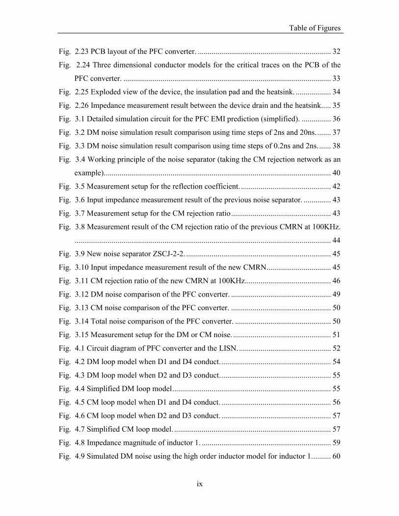
Table of Figures
ix
Fig. 2.23 PCB layout of the PFC converter. .................................................................... 32
Fig. 2.24 Three dimensional conductor models for the critical traces on the PCB of the
PFC converter. .......................................................................................................... 33
Fig. 2.25 Exploded view of the device, the insulation pad and the heatsink. .................. 34
Fig. 2.26 Impedance measurement result between the device drain and the heatsink..... 35
Fig. 3.1 Detailed simulation circuit for the PFC EMI prediction (simplified). ............... 36
Fig. 3.2 DM noise simulation result comparison using time steps of 2ns and 20ns........ 37
Fig. 3.3 DM noise simulation result comparison using time steps of 0.2ns and 2ns....... 38
Fig. 3.4 Working principle of the noise separator (taking the CM rejection network as an
example).................................................................................................................... 40
Fig. 3.5 Measurement setup for the reflection coefficient. .............................................. 42
Fig. 3.6 Input impedance measurement result of the previous noise separator. .............. 43
Fig. 3.7 Measurement setup for the CM rejection ratio................................................... 43
Fig. 3.8 Measurement result of the CM rejection ratio of the previous CMRN at 100KHz.
................................................................................................................................... 44
Fig. 3.9 New noise separator ZSCJ-2-2. .......................................................................... 45
Fig. 3.10 Input impedance measurement result of the new CMRN................................. 45
Fig. 3.11 CM rejection ratio of the new CMRN at 100KHz............................................ 46
Fig. 3.12 DM noise comparison of the PFC converter. ................................................... 49
Fig. 3.13 CM noise comparison of the PFC converter. ................................................... 50
Fig. 3.14 Total noise comparison of the PFC converter. ................................................. 50
Fig. 3.15 Measurement setup for the DM or CM noise. .................................................. 51
Fig. 4.1 Circuit diagram of PFC converter and the LISN................................................ 52
Fig. 4.2 DM loop model when D1 and D4 conduct......................................................... 54
Fig. 4.3 DM loop model when D2 and D3 conduct......................................................... 55
Fig. 4.4 Simplified DM loop model................................................................................. 55
Fig. 4.5 CM loop model when D1 and D4 conduct. ........................................................ 56
Fig. 4.6 CM loop model when D2 and D3 conduct. ........................................................ 57
Fig. 4.7 Simplified CM loop model. ................................................................................ 57
Fig. 4.8 Impedance magnitude of inductor 1. .................................................................. 59
Fig. 4.9 Simulated DM noise using the high order inductor model for inductor 1.......... 60

Table of Figures
x
Fig. 4.10 Verification of the DM noise simulation result using inductor 1. .................... 61
Fig. 4.11 Impedance magnitude of inductor 2. ................................................................ 61
Fig. 4.12 Verification of the DM noise simulation result using inductor 2. .................... 62
Fig. 4.13 Insulation pad 1 and the impedance measurement result of CCM with pad 1. .. 63
Fig. 4.14 Insulation pad 2 and the impedance measurement result of CCM with pad 2. .. 64
Fig. 4.15 CM noise simulation and measurement results using different insulation
materials. ................................................................................................................... 64
Fig. 4.16 Measured VDS waveform.................................................................................. 67
Fig. 4.17 Using a trapezoidal waveform to approximate the VDS waveform. ................. 67
Fig. 4.18 The envelope of the frequency domain spectrum of the trapezoidal waveform.
................................................................................................................................... 68
Fig. 4.19 VDS falling time Tf measurement result with the 3Ω gate resistor. .................. 71
Fig. 4.20 VDS falling time Tf measurement result with the 15Ω gate resistor. ................ 71
Fig. 4.21 DM noise measurement result with the 3Ω gate resistor.................................. 72
Fig. 4.22 DM noise measurement result with the 15Ω gate resistor................................ 72
Fig. 4.23 DM noise measurement result comparison for the case with the 15Ω gate
resistor and the case with the 3Ω gate resistor.......................................................... 73
Fig. 4.24 DM noise measurement result with the 51Ω gate resistor................................ 74
Fig. 4.25 DM noise measurement result comparison for the case with the 51Ω gate
resistor and the case with the 15Ω gate resistor........................................................ 75
Fig. 4.26 CM noise measurement result with the 3Ω gate resistor.................................. 76
Fig. 4.27 CM noise measurement result with the 15Ω gate resistor................................ 76
Fig. 4.28 CM noise measurement result comparison for the case with the 3Ω gate resistor
and the case with the 15Ω gate resistor. ................................................................... 77
Fig. 4.29 CM noise measurement result comparison for the case with the 15Ω gate
resistor and the case with the 51Ω gate resistor........................................................ 78
Fig. 4.30 Falling time of the IRFP460A VDS waveform with Rg=15ohm. ..................... 79
Fig. 4.31 Falling time of the SPW20N60C3 VDS waveform with Rg=15ohm. ............... 80
Fig. 4.32 DM noise comparison of the two different devices’ combinations with
Rg=15ohm. ............................................................................................................... 81

Table of Figures
xi
Fig. 4.33 Falling time of the IRFP460A VDS waveform with Rg=51ohm. ..................... 82
Fig. 4.34 Falling time of the SPW20N60C3 VDS waveform with Rg=51ohm. ............... 82
Fig. 4.35 DM noise comparison of the two different devices’ combinations with
Rg=51ohm. ............................................................................................................... 83
Fig. 4.36 The PFC circuit diagram with a capacitor Crec at the output side of the diode
bridge. ....................................................................................................................... 84
Fig. 4.37 DM loop with balanced input wires. ................................................................ 85
Fig. 4.38 CM loop with balanced input wires.................................................................. 86
Fig. 4.39 DM loop with unbalanced input wires. ............................................................ 86
Fig. 4.40 CM loop with unbalanced input wires.............................................................. 87
Fig. 4.41 Measurement setup and the DM noise measurement results comparison for the
balanced and unbalanced input wires. ...................................................................... 88
Fig. A. 1 Case study for structural inductance characterization. ...................................... 95
Fig. A. 2 Major structural inductance of the Active IPEM............................................... 96
Fig. A. 3 Impedance measurement curves of Step 1 and the equivalent circuit. .............. 97
Fig. A. 4 Impedance measurement curves of Step 4 and the equivalent circuit. .............. 97
Fig. A. 5 Comparison of structural inductance extraction results..................................... 99
Fig. A. 6 DBC pattern and the structural capacitance (device not incorporated). .......... 100
Fig. A. 7 Measured impedance between trace P and the back plane (without devices) . 101
Fig. A. 8 Devices on the DBC board. ............................................................................. 102
Fig. A. 9 Capacitance model of the structure at 8MHz. ................................................. 102
Fig. A. 10 Measurement results comparison between different terminals and the back
plane (with devices). ............................................................................................... 103
Fig. A. 11 Measurement results comparison between trace P and the back plane for
different states of the devices.................................................................................. 103
Fig. A. 12 Measurement results and the approximation of CTOTAL ................................ 105
Fig. A. 13 External inductor L1 in parallel with S1 to produce resonance. .................... 105

Table of Figures
xii
Fig. A. 14 Comparison of the impedances across the P and O terminals, without L1 (left)
and with L1 (right)................................................................................................... 106
Fig. A. 15 Comparison of Z(pb) without L1 (left) and with L1 (right). .......................... 106
Fig. A. 16 External inductor L2 in parallel with S2 to produce resonance ..................... 107
Fig. A. 17 Impedances across the O and N terminals with L2=10uH............................. 108
Fig. A. 18 Impedances across the O and N terminals with L2=1mH.............................. 109

List of Tables
xiii
List of Tables
Table 2-1 Verification result of the Saber model of SPW20N60C3 MOSFET................ 18
Table 2-2 Parasitic inductance extraction results for the traces in Fig. 2.20. .................. 31
Table 3-1 CM rejection ratio comparison of the previous CMRN and the new CMRN. . 46
Table 4-1 Comparison of the frequencies of the impedance peaks and valleys of the two
inductors.................................................................................................................... 62
Table A - 1 Structural inductance characterization results. .............................................. 98
Table A - 2 Structural capacitance measurement and calculation. ................................. 101
Table A - 3 Structural capacitance value determination................................................. 110
Chapter 1
1
Chapter 1 Introduction
1.1. Background
To power the next generation of information technology, the distributed power system
(DPS) architecture has been widely adopted as an industry practice. Compared to the
centralized power system, the DPS has many advantages, such as thermal management
and reliability [A 1-A 2]. In the DPS, the front-end module needs to convert the ac-line
voltage into a low dc output voltage, such as 48V. Most of the existing front-end
converters used in DPS applications adopt a two-stage approach. The first stage of the
front-end converter provides the power factor correction (PFC), and the second stage
provides isolation and tight regulation of the DC output voltage.
Power quality is a major concern, and stringent international requirements, such as the
IEC 1000-3-2 [C 8], have been released to limit the harmonic currents drawn by the off-
line equipment. As a result, PFC techniques have become common practice in the front-
end DPS converter in order to guarantee that the harmonic components are kept low and
the input current waveform is close to sinusoidal [A 3-A 4]. The circuit diagram of the
CCM PFC converter is shown in Fig. 1.1.
Fig. 1.1 Circuit diagram of the PFC converter.

Chapter 1
2
Besides the regulations with respect to the total harmonic distortion (THD), standards for
high-frequency electromagnetic interference (EMI) limits, such as EN55022, are also
requirements for the DPS [C 9-C 10]. The high frequency conducted and radiated EMI
can cause polluted signals into other electronics circuitry and equipment. To control and
suppress the high frequency EMI generated from the DPS, a clear understanding of the
mechanisms for EMI generation and propagation is undoubtedly a fundamental basis.
Since the PFC converter is the first stage of the front-end converter, its impact to the EMI
spectrum is a fundamental knowledge base for understanding the EMI of the whole front-
end converter and the DPS system. Based on the literature surveyed in Section 1.2, the
subject of PFC EMI has not been fully explored in previous literatures. Therefore, this
thesis tries to tackle this problem by investigating this aspect in more detail.
1.2. Literature Review
Since the PFC techniques are widely adopted in the DPS, a lot of research works have
been carried out for the PFC EMI [B 1-B 7].
In [B 1], the EMI spectrum of a discontinuous conduction mode (DCM) PFC converter is
predicted using a simulation circuit in Saber. The simulated DM, CM and total noise
matches the measurement result quite well, which demonstrates the possibility of using a
simulation software to predict EMI noise. It also shows that modeling and
characterization techniques are very important for this approach. However, CCM PFC is
the common practice in DPS systems. Investigation of the EMI behavior of the CCM
PFC converter is therefore a meaningful work.
Time domain simulation is not the only approach to analyze the EMI noise. Many of the
previous papers ([B 2, D 6]) for EMI analysis also adopt a frequency domain approach. A
frequency domain method for PFC EMI analysis is described in [B 2]. In that paper, the
noise sources and all of the other circuit components are expressed as functions in the
Chapter 1
3
frequency domain and the final result of the predicted EMI spectrum is mathematically
calculated by solving matrixes of these functions.
There are many papers that discussed the conducted EMI issues in Boost PFC design and
[B 3] is one of them. A lot of design considerations are discussed in that paper, such as
the printed circuit board (PCB) layout, the effect of gate snubber, the shield inserted
between the device and the heatsink, and the heatsink grounding connection. This
information is very useful in the design process for compliance of the EMI standard.
In [B 4], two loop models are presented to explain the CCM PFC EMI. Improved filter
design is also proposed based on the noise loop models.
There are also other papers discussing the EMI behavior of the PFC converter and some
examples are listed below. In [B 5], the design trade-off between the conducted EMI
noise levels and the thermal behavior of a boost PFC circuit are analyzed. In [B 6], a
method is proposed for determining of the first harmonic in the DM noise spectrum of a
series of power factor preregulator circuits. In [B 7], the idea of adding an auxiliary anti-
phase winding of the boost inductor is proposed and realized in a boost PFC converter.
This circuit exhibits reduced CM noise compared to the conventional boost PFC circuit.
1.3. Objective of this Study
The main objective of this thesis is to predict the conducted EMI of the CCM PFC circuit
based on a set of modeling and characterization techniques in the medium and high
frequency ranges. As specified by [C 10], the frequency range for testing the conducted
EMI is from 150KHz to 30MHz, which is mainly the medium and high frequency ranges
as defined in many electronics textbooks, [C 4]. Time domain waveform simulations and
fast fourier transform (FFT) techniques are the tools to accomplish this goal. The
following paragraphs outline the importance and significance of this study.

Chapter 1
4
Firstly, a better understanding of the PFC EMI will be an outcome of this work.
Important knowledge, such as the model for the noise loops and the dominant factors that
influence the noise level and envelope, can be obtained. This information can help the
engineer to control and suppress the PFC EMI in the design stage.
Secondly, having a simulation circuit model for the PFC converter, the network
parameters of the circuit components can be easily changed to check whether it is
beneficial or detrimental to the EMI. Compared to a trial-and-error approach, this
alternative will definitely be a time-saving and cost-effective approach.
Thirdly, with the accurately predicted differential-mode (DM) and common-mode (CM)
noise, the EMI filter can be designed before the hardware is constructed. When the
conducted EMI generated from the DPS is higher than the limits specified by the
standards, EMI filters need to be inserted between the input AC bus and the PFC stage, so
that the EMI of the DPS can be attenuated to a level lower than that specified by the
standards. The classic method for the design of the PFC filter is based on the DM and
CM noise without the EMI filter, in other words, the bare noise. The bare noise will be
compared to the EMI standards so that the EMI filter designer can determine how much
attenuation is required to meet the EMI standard. And the values of the inductors and
capacitors will be designed according to the attenuation requirements. Having the
accurately modeled conducted EMI noise for the PFC converter, the possibility of an
over-designed EMI filter will be reduced, and thus the EMI filter will be compact and
cost-effective.
1.4. Thesis Organization
In Chapter 2, a set of modeling and characterization techniques in the medium and high
frequency ranges are introduced. A detailed simulation circuit is necessary to accurately
predict the EMI noise using the time domain simulation method. So, most of the circuit
components such as the inductor, the capacitors, the devices, the power module and the

Chapter 1
5
layout parasitic parameters have to be carefully modeled and characterized. For better
description, the techniques can be categorized into four levels, namely component-level,
device-level, module-level and system-level.
Based on the modeling and characterization techniques, the EMI noise prediction results
will be presented in Chapter 3. The simulated EMI noise is compared to the measured
EMI noise for the DM, CM and total noise aspects. Two important issues for this work,
simulation time step selection and noise separator selection, will also be addressed in this
chapter.
The good match between simulated and measured EMI noise presented in Chapter 3 is a
desired result. However, this result itself does not provide a clear explanation of the EMI
generation and propagation mechanism. In Chapter 4, further investigation is performed
in order to provide deeper insight into the PFC EMI. The DM and CM loop models of
PFC EMI are proposed in this chapter for describing the noise generation and
propagation mechanisms. The effects of the PFC inductor, the parasitic capacitances
between the MOSFET drain and the heatsink, the rising/falling time of MOSFET VDS
voltage and the input wires are also analyzed.
The conclusions and the suggestions for future work are given at the end of this thesis.

Chapter 2
6
Chapter 2 Modeling and Characterization Techniques in the Medium and High Frequency
Ranges
2.1. Overview of the Modeling and Characterization Techniques
The circuit diagram of CCM PFC converter is shown in Fig. 1.1. The hardware
implementation of the converter is far more complex than its schematic. As shown in Fig.
2.1, the hardware consists of many circuit components, such as the inductor, the
capacitors, the MOSFET and the diode.
For the purpose of conducted EMI modeling, it is easy to imagine that the circuit diagram
must be converted into a far more complex and detailed simulation circuit that can cover
the essential EMI characteristics of the real hardware up to 30MHz. For different
components, devices, modules and system parasitic parameters, one must use different
modeling and characterization techniques to find suitable models, so that the detailed
system simulation circuit can finally be obtained. And this is also the common practice in
many of the previous literatures about the EMI modeling [B 1, B 2, D 8].
Fig. 2.1 Photograph of the PFC converter hardware.

Chapter 2
7
In the following sections of this chapter, the modeling and characterization techniques
will be categorized into component-level modeling, device model verification, module-
level characterization and system-level parasitic parameters’ modeling.
The PFC circuit is the case study in this thesis; however, the same modeling and
characterization techniques can also apply to other power electronics circuits for system-
level EMI analysis and prediction.
Fig. 2.2 PFC circuit diagram, including layout inductance and parasitic capacitance at the device
drain node.
Fig. 2.2 shows a PFC circuit diagram which is similar to the one in Fig. 1.1, except that
some stray inductance associated with the layout, and the parasitic capacitance at the
device drain node have been included.
Component-level modeling refers to the modeling techniques for normal discrete passive
components, such as the PFC inductor and the output capacitors. Considering that the
purpose of modeling here is to obtain a simulation model in the frequency range as the

Chapter 2
8
EMI standards specifies, the thesis focuses on obtaining an equivalent circuit to represent
its impedance characteristics for those frequencies.
Devices such as the MOSFETs and the diodes are the components that perform the
switching action in the circuit. Because the switching waveform associated with them is
responsible for the noise, device models are also essential parts of the simulation circuit.
In this thesis, the model of the MOSFET is provided by the manufacturer, and the model
of the diode is developed using the Diode Tool function in the circuit simulation software
package, Saber. Before using them in the simulation circuit, the accuracy of the models is
verified.
Module-level characterization refers to the extraction of the parasitic parameters within a
power electronics module. These parasitic parameters affect the high frequency behavior
of the module; thus, they are important for EMI simulation. Software extraction and
measurement-based extraction are the two methods for handling this job. Each of these
two methods has its advantages and disadvantages. One needs to consider the specific
application to decide which method is applicable.
System-level parasitic parameters refer to the printed circuit board (PCB) layout parasitic
inductances, and the capacitances between the drain node of the MOSFET and the
heatsink. As pointed out by some of the previous literature [B 1, D 6], the parasitic
parameters of the PCB layout will impact the EMI spectrum. Parasitic parameters
extraction using dedicated software is a common method for taking their effects into
account. The discussion in Chapter 4 will show that the parasitic capacitance between the
device drain and the heatsink, CCM, provides a path for the noise current to flow, so its
impact cannot be neglected. Impedance measurement is a useful method for determining
the value of this capacitance.

Chapter 2
9
2.2. Component Level Modeling and Characterization Inductors and capacitors are common passive components in power electronics circuits.
Inductors are the components that store magnetic field energy, and capacitors are the
components that store electric field energy.
To obtain the simulation model for inductors and capacitors, one usual approach is to
measure the impedance using an impedance analyzer. An equivalent circuit network can
then be found from the measured impedance magnitude and phase curves. A curve-fitting
method can be used to determine the parameters’ values in the equivalent circuit.
2.2.1. PFC Inductor Modeling
The inductor used in a 100KHz PFC circuit is shown in Fig. 2.3. The core is 77083A
core from Magnetics Corporation with two cores stacked together. The 49-turn winding
employs AWG16 wire.
Fig. 2.3 Inductor for the 100KHz PFC circuit.
Using an impedance analyzer Agilent 4294A, the impedance magnitude and phase can be
measured in the frequency range up to 110MHz. The magnitude curve is shown on the
left side of Fig. 2.4 and the phase curve is shown on the right side of Fig. 2.4 for
frequencies up to 30MHz.

Chapter 2
10
Fig. 2.4 Impedance magnitude and phase of the PFC inductor.
Fig. 2.4 shows that there are two peaks (f1 and f3) and one valley (f2) in the magnitude
curve up to 30MHz. The first impedance valley (f2) and the second impedance peak (f3)
are in the frequency range higher than 10MHz. According to the shape of the magnitude
curve and phase curve below 10MHz, the equivalent network in Fig. 2.5 should be able
to approximate the impedance characteristics up to 10MHz. The model includes the
inductance L1, the capacitance C1 and two resistances, R1 and R2. The resistance R1 is in
series with the inductance L1. Choosing the appropriate value for R1 can make the
impedance characteristic of the equivalent circuit more closely match the measurement
results in low frequency. The resistance R2 is in parallel with other parts of the equivalent
circuit. Choosing the appropriate value for R2 can make the impedance characteristic of
the equivalent circuit more closely match measurement result at f1, the resonant
frequency of L1 and C1.

Chapter 2
11
Fig. 2.5 A second order model for the inductor.
Using the second order model, the first peak in the impedance curve can be well matched,
as depicted in Fig. 2.6. However, this second order model does not represent the first
impedance valley at f2 or the second impedance peak at f3. A more complex, higher order
model has to be used to represent the impedance characteristics of the PFC inductor up to
30MHz.
Fig. 2.6 Second order model for the 100KHz PFC inductor and the impedance comparison between
the model and the measurement.

Chapter 2
12
The measured impedance curves in Fig. 2.4 show that the phase is about 0 degree
whenever the magnitude reaches a peak or a valley, which is the characteristic of series
resonance or parallel resonance. The L1 and C1 in the second order model shown in Fig.
2.5 account for the parallel resonance at f1. Following the same concept, one can add L2,
which is in series connection with the second order model shown in Fig. 2.5 to produce
the series resonance with C1 at f2, as illustrated in Fig. 2.7. Because the value of C1 is
already known, the value of L2 can be calculated from the value of f2 according to the
equation 12
2 21CL
fπ
= . Because the frequency of f2 is about seven times higher than
the frequency of f1, adding L2 to the original second order equivalent circuit will not have
much influence on the frequency of f1. From the comparison made in Fig. 2.7, better
match can be obtained between the measurement and the model. However, it is still not
good enough to match the measurement curves up to 30MHz.
Fig. 2.7 Adding L2 to the original second order inductor model.

Chapter 2
13
Following the same concept, one can add another capacitor in parallel with L2, which will
lead to the second impedance peak at f3. However, the frequency of f2 is close to that of
f3. So, adding C2 to this circuit will change the frequency of f2. Some fine tune process is
necessary to determine the appropriate values of the inductors and resistors. For this
purpose, L2 is divided into two inductors, L21 and L22, and the values of L21, L22 and C2
need to be adjusted. The final result of the fine tune process is shown in Fig. 2.8.
As can be seen in Fig. 2.8, the impedance characteristics of the equivalent circuit match
the measurement results up to 30MHz. And the equivalent circuit will be used in the final
simulation circuit for the PFC EMI prediction.
Fig. 2.8 Higher order inductor model.

Chapter 2
14
2.2.2. Capacitor Modeling
Compared to the modeling of the PFC inductor, the modeling for the output capacitors is
easier. In most cases, the simple equivalent network in Fig. 2.9 will provide a good
approximation of the impedance characteristics up to 30MHz for the capacitors. This
model includes the equivalent series inductance (ESL) and the equivalent series
resistance (ESR) of the capacitor.
Fig. 2.9 Model for the capacitors.
Fig. 2.10 Using the equivalent circuit model to approximate the capacitor’s impedance.

Chapter 2
15
An example is shown in Fig. 2.10. It is the curves for one of the high voltage ceramic
capacitors at the DC output side. In the magnitude plot, there are two closely matched
curves. One is obtained from measurement data, and the other is from a simulation using
the equivalent circuit in Fig. 2.9. The values of the equivalent circuit parameters are
calculated using a curve fitting method by the impedance analyzer automatically, and
they are shown in the dashed-line circle in Fig. 2.10. In the phase plot, the curves from
the measurement data and the equivalent circuit are also closely matched.
Fig. 2.11 Impedance characteristics of the output electrolytic capacitor.
The impedance characteristics of the output electrolytic capacitor and the equivalent
circuit parameters are shown in Fig. 2.11. The equivalent circuit simulation curves match
well with the measurement curves. The ESL value of the electrolytic capacitor is

Chapter 2
16
measured to be 10.6nH, which is larger than that of the output ceramic capacitor, 4.0nH.
This is the reason for that the high frequency performance of the electrolytic capacitor is
not as good as the ceramic capacitor. In the real hardware, another ceramic capacitor is
paralleled with the one shown in Fig. 2.10 to help further reducing the voltage stress and
obtain better filtering effect. The capacitance, ESR and ESL of it are measured to be
125.9nF, 26.2mΩ and 7.0nH, respectively.

Chapter 2
17
2.3. Device Model Verification
The switching actions of the MOSFET and diode are the primary sources of the
conducted EMI, so the models for the devices are very important in the simulation circuit.
The Saber model for the MOSFET in the PFC circuit is provided by the manufacturer.
The model for the diode in the PFC circuit is developed using the Diode Tool function of
Saber. Before using them in the final simulation circuit, these models need to be verified.
Because the verification work is done by Dr. Zhiguo Lu and Dr. Wei Dong instead of the
author, only the verification results are presented here and the verification process will
not be discussed in detail.
2.3.1. MOSFET Model Verification
The power MOSFET in the discrete PFC circuit is from Infineon Corporation and the part
number is SPW20N60C3.The accuracy of the model is verified in six aspects including:
(1) Gate charge characteristics, (including Qgs, Qgd, Qg and gate charge plateau
voltage)
(2) Gate threshold voltage,
(3) Output characteristic ID=f(VDS),
(4) On-state resistance,
(5) Transconductance gfs ,
(6) Dynamic capacitance
In order to verify the afore-mentioned characteristics, a series of simulation circuits were
developed in Saber using the manufacturer’s SPW20N60C3 MOSFET model. Based on
these simulation circuits, the characteristics of the model can be obtained. The simulated
characteristics were then compared to the data sheet values and curves. A comparison of

Chapter 2
18
gate charge, gate threshold voltage, on-state resistance and transconductance are given in
Table 2-1.
Table 2-1 Verification result of the Saber model of SPW20N60C3 MOSFET.
Data sheet Model simulation
result Error
Gate charge plateau
voltage 5.5 (V) 5.21 (V) 5.3%
Qgs 11 (nC) 10 (nC) 9.1%
Qgd 33 (nC) 34 (nC) 3.0%
Qg 87 (nC) 85 (nC) 2.3%
Threshold voltage
2.1 (V) minimum
3.0 (V) typical
3.9 (V) maximum
3.1 (V)
On-state resistance 0.16 (ohm) 0.14 (ohm) 12.5%
Transconductance 17.5 (S) 18.8 (S) 7.4%
The verification of the output characteristic ID=f(VDS) is shown in Fig. 2.12.
Fig. 2.12 Verification result of the output characteristic of the MOSFET model.

Chapter 2
19
The verification result of the dynamic capacitances is shown in Fig. 2.13.
Fig. 2.13 Verification result of the dynamic capacitances of the MOSFET model.
From the comparison results in Table 2-1, Fig. 2.12 and Fig. 2.13, the accuracy of the
SPW20N60C3 MOSFET Saber model is good.
2.3.2. Diode Model Verification
The diode in the PFC circuit is also a product from Infineon Corporation. The part
number is SDT06S60. Using the Diode Tool Function in Saber, a simulation model for
the diode can be developed. The accuracy of the developed model is also verified. A
comparison between the forward characteristic from the data sheet and that obtained
using Saber model is given in Fig. 2.14. From the comparison result in Fig. 2.14, the
forward characteristic of the model are very close to the curves from the data sheet.

Chapter 2
20
Fig. 2.14 Verification result of the forward characteristic of the diode model.
2.3.3. Switching Waveform Comparison
In addition to the model verification work in Section 2.3.1 and Section 2.3.2, switching
behavior of the SPW20N60C3 MOSFET and the SDT06S60 diode are also investigated.
A device test circuit is constructed for this purpose and the corresponding simulation
circuit is developed in Saber for it.
The simulation circuit for the device test circuit is shown in Fig. 2.15, which includes the
models for the SPW20N60C3 MOSFET and the SDT06S60 diode. The MOSFET is
driven by a square wave gate signal. When the MOSFET is ON, the inductor l1 is charged
by the 400V DC voltage. When the MOSFET is OFF, the energy in the inductor l1 is
discharged through the diode. The 250mΩ resistor in series with the MOSFET is the
current-sensing resistor for measuring the device current, ID. Using this configuration, the
switching behavior of the MOSFET and the diode models can be verified.

Chapter 2
21
Fig. 2.15 Simulation circuit for the device test circuit.
The waveforms at the turn-on transient are shown in Fig. 2.16. The simulated VDS and ID
waveforms are very similar to the measurement waveforms on the right side. Another
curve in the measurement waveforms is the measured turn-on loss by integrating the
product of the voltage and the current. The measured turn-on loss is 314uJ, which is close
to the simulated turn-on loss 290uJ.

Chapter 2
22
Fig. 2.16 Switching waveform comparison at the turn-on transient.
The waveforms at the turn-off transient are shown in Fig. 2.17. The simulated VDS and ID
waveforms are also very similar to the measurement waveforms on the right side. The
measured turn-off loss is 200uJ, whereas the simulated turn-on loss 263uJ.
Fig. 2.17 Switching waveform comparison at the turn-off transient.
Based on all of the verification results of the MOSFET model and the diode model, the
accuracy of the models should be good for the purpose of the conducted EMI simulation.

Chapter 2
23
2.4. Module Level Modeling and Characterization
Modularization and integration are the future trends for power electronics [D 1-D 2]. By
using advanced packaging technologies, the conventional discrete devices and
components can be packaged into one module. Compared to the discrete approach, the
benefits obtained by integration and modularization include better electrical performance,
better thermal performance and higher power density.
The integrated power electronics modules (IPEM) concept was proposed by CPES [D 1-
D 4]. Considering the fundamental motivation, the IPEM is expected to be a
standardized, off-the-shelf unit that packages the power electronics components (devices,
circuits, controls, sensors and actuators) together into one module. IPEMs will eliminate
much of the cost and time-to-market delays of custom circuits and provide lower
production costs due to economies of scale.
Demonstrative prototypes of the IPEM were developed and one of them are shown in
Fig. 2.18. This IPEM is successfully used in DC/DC converters of kilo-watt power level
successfully. The IPEMs are developed using advanced packaging technologies and
incorporate various functions, including one or more semiconductor devices, into one
integrated structure that features a compact layout with small structural parameters.
Fig. 2.18 A prototype of DC/DC IPEM.

Chapter 2
24
Accompanying with the construction and fabrication of the IPEM, the requirement for the
IPEM characterization and modeling is raised. With the integration technology, smaller
layout parasitic parameters are expected and accurate characterization methods are
required to test this expectation. The methods for developing the models of the parasitic
parameters within the IPEM can be divided into two major categories. One is an
measurement-based method and the other is a software extraction method.
2.4.1. Software Characterization
Today, software tools are available for calculating the parasitic parameters using finite
element analysis (FEA) or the partial element equivalent circuit (PEEC) method [D 5-D
7]. Software packages such as Maxwell Q3D, Inca and StatMod have been used in
previous literatures and they contribute to many research accomplishments. One of the
advantages of these methods is that once the 2D or 3D models are built in the software,
one can easily change the dimensions and the material characteristics to see whether this
is beneficial or detrimental to the final design goal. In all of these software extraction
applications, detailed geometric data and material properties are required for accurate
results using this technique. This situation therefore limits the application of the software
extraction methods, since such detailed information is not always available for a
commercial power electronics module, which has been packaged as a black box. The
problem is further complicated by the non-linear frequency dependency of the structural
inductances and resistances. Furthermore, drawing an accurate geometric model for a
complex structure is usually a time-consuming process. The FEA calculation time may
also be long.

Chapter 2
25
2.4.2. Measurement-Based Method
2.4.2.1. Measurement-Based Methods in Previous Literature
As an alternative to software extraction, measurement-based methods or empirical
methods have been explored. One example is the time domain reflectometry (TDR)
method, which applies the transmission line theory to parasitic extraction [D 8]. This
method is measurement-based, and is independent of the internal geometry and material
information. A disadvantage of commercial TDR instruments is that they are normally
designed for connector impedances of typically 50Ω. Accuracy may therefore be affected
when the characteristic impedance of the measured transmission line structure deviates
significantly from the matched value.
Previous reports [D 10-D 11] discuss measurement-based methods for extracting the lead
inductances and the device’s intrinsic capacitances. However, the capacitances between
the top layer traces and back plane copper within the IPEM are not considered. These
capacitances provide paths for CM noise propagation, and therefore they need to be
extracted, too.
2.4.2.2. Proposed Measurement-Based Method
A new measurement-based method is proposed for high-frequency characterization of the
active IPEM [D 16]. This method uses lumped, linear parameters to approximate the
effects of nonlinear parameters. The model parameters can be extracted through a simple
set of impedance measurements, and the basic principles of this approach are simple and
intuitive. Both the structural inductances and the structural capacitances can be extracted
using this method. In a case study, the extraction results obtained using the proposed
measurement-based method of a prototype IPEM are compared with those obtained using
a commercial software tool, the Maxwell Q3D parameter extractor. A frequency domain

Chapter 2
26
circuit simulation is performed using Saber software for this comparison. Close match
between the results of the proposed measurement-based method and those from the
Maxwell Q3D is obtained.
For the detailed description of this measurement-based method, one can refer to
Appendix 1 at the end of this thesis.

Chapter 2
27
2.5. System Level Modeling and Characterization
When designing power electronics circuits, it is important to pay attention to the PCB
layout. Well-designed layout reduces voltage stress and ringing, and thus can alleviate
high frequency EMI noise. On the other hand, if the layout is not carefully designed, the
voltage stress and the ringing can be severe, sometimes can even cause circuit
malfunction due to the interaction between the power stage and the control circuit. To
take the effect of the layout into account, the parasitic inductances associated with the
traces need to be extracted.
For some of the common power MOSFET packages like TO-247 and TO-220, heatsinks
are often attached to the backside of the device to offer better thermal dissipation. Due to
safety requirement, insulation material is inserted between the heatsink and the backside
of the MOSFET. In many cases, the backside of the device is connected to the MOSFET
drain. Therefore, parasitic capacitances will be introduced between the device drain and
the heatsink. In Section 4.3, this capacitance will be proved to play an important role in
CM noise propagation. For simplicity, the term CCM will be used in the thesis to represent
this capacitance.
In this section, the modeling and characterization methods for the trace layout parasitic
inductances and the CCM will be described.
2.5.1. Layout Parasitic Parameters Modeling
Many software packages have been developed for layout parasitic inductance extraction.
Examples are Maxwell Q3D [D 5], Inca [D 6], and Fasthenry [D 12].

Chapter 2
28
Due to its advantages, the Maxwell Q3D is selected as the layout parasitic inductance
extraction software in this thesis. This software provides fast calculation for the user. In
most of the application cases, the parasitic inductance extraction result is accurate, [D
14]. The parasitic inductance extracted by this software can be easily incorporated into a
Saber model. This software can be run in both Windows and Unix operating system,
which is very convenient for the users.
2.5.1.1. Trace inductance extraction process of Maxwell Q3D
The process for extracting the layout parasitic inductance using Maxwell Q3D is
described as follows. Each trace on the PCB can be considered as a conductor. For each
trace, a three-dimensional conductor model can be drawn based on the dimensions of the
trace. For example, traces 1 and 2 in Fig. 2.19 can be treated as two conductors in the
Maxwell Q3D; their three-dimensional conductor models in the Maxwell Q3D software
environment are shown in Fig. 2.20.
Fig. 2.19 Traces 1 and 2 on a PCB.

Chapter 2
29
Fig. 2.20 Maxwell Q3D conductor models for traces 1 and 2.
Before the Maxwell Q3D software begins the calculation to obtain the values of the trace
parasitic inductance, the user needs to define the nodes by which the current will flow
into the conductor, as well as those by which the current will flow out of the conductor.
For example, pad A in Fig. 2.20 is the node by which the current will flow into trace 1,
and pad B is that by which the current will flow out of trace 1. One point that needs to be
clarified is that the current directions at nodes A to D are only defined for the purpose of
parasitic inductance calculation in the Maxwell Q3D. They may not be the same as the
current directions in the real circuit.
After the conductor models are built and the nodes by which the current will flow in and
out are defined, the Maxwell Q3D can begin the computation to calculate the self
inductance and mutual inductance of the traces. The self inductance and the mutual
inductance in the Maxwell Q3D are partial inductance, because this software uses the
PEEC method [D 15] to represent the extraction results. Although the concept of the
partial inductance is different from that of the conventional loop inductance, the loop

Chapter 2
30
inductance can be represented by the partial inductance. One example is shown in Fig.
2.21.
Fig. 2.21 Conductors for inductance calculation.
Assuming that the four conductors labeled as 1-4 in Fig. 2.21 form a loop, and current
I is flowing in the loop, the conventional method calculates the magnetic flux Φ in the
loop area and then loop inductance can be calculated as I
L Φ= . Using the PEEC method,
the loop inductance L can also be expressed using the self inductance and the mutual
inductance of the four conductors in the form of the following equation:
244422133311 22 pppppploop LLLLLLL −++−+= . ( 2.1 )
In this equation, the 11pL , 22pL , 33pL and 44pL are self inductance, which can be obtained
directly from the result of Maxwell Q3D. The 13pL and 24pL are the mutual inductance,
which are also calculated by Maxwell Q3D. Note that 3113 pp LL = and 4224 pp LL = .

Chapter 2
31
Because conductors 1 and 3 are perpendicular to conductors 2 and 4, the mutual
inductance between conductors1/3 and conductors 2/4 are neglected.
For traces 1 and 2 in Fig. 2.20, the inductance extraction result is shown in Table 2-2.
Table 2-2 Parasitic inductance extraction results for the traces in Fig. 2.20.
L11=63.2nH L12=12.9nH
L21=12.9nH L22=54.7nH
Because pad B of trace 1 and pad C of trace 2 are close to each other, they can be
connected by a wire so that these two traces form a loop starting from pad A and ending
at pad D. The loop inductance can be derived from the self inductances and mutual
inductance as 92.1nH as follows:
nHLLLLloop 1.922 122211 =−+= . ( 2.2 )
The inductance of the loop starting from pad A and ending at pad D can also be measured
by an impedance analyzer for verification purposes. The impedance measurement result
in Fig. 2.22 is measured when pads B and C are connected with a 1Ω resistor, so at low
frequencies the impedance characteristic is resistive. However, in the MHz range, the
impedance curves become inductive since the phase curve is approaching 90°. And the
loop inductance value can be obtained using the equivalent circuit function of the
impedance analyzer and the final result is 84.4nH, as indicated in the dashed-line circle
located on the left side of Fig. 2.22. Compared to the measurement value of 84.4nH, the
loop inductance value derived from Table 2-2, 92.1nH, is within 10% error margin. This
case shows that the accuracy of the Maxwell Q3D inductance extraction is acceptable.

Chapter 2
32
Fig. 2.22 Impedance measurement result between pads A and D in Fig. 2.20 (With a 1ΩΩΩΩ resistor
connecting pads B and C).
2.5.1.2. Trace inductance extraction for the PCB of the PFC Converter
The PCB layout for the PFC converter is shown in Fig. 2.23.
Fig. 2.23 PCB layout of the PFC converter.

Chapter 2
33
There are many traces on the PCB, but only the inductances of critical traces need to be
extracted. Critical traces include those involved in large-current commutation loops, since
they are related to ringing frequency and overshoot amplitude. Critical traces also include
the MOSFET gate traces, since they will affect the switching speed.
Following the extraction process described in Section 2.5.1.1, three-dimensional
conductor models are built for the critical traces of the PCB of the PFC converter, as
shown in Fig. 2.24.
Fig. 2.24 Three dimensional conductor models for the critical traces on the PCB of the PFC
converter.
After defining the current flow-in and flow-out nodes for these conductors, the Maxwell
Q3D software can calculate the self inductance and mutual inductance for these traces.
The extraction results are incorporated into the Saber simulation circuit for conducted
EMI simulation.

Chapter 2
34
2.5.2. Modeling of the Capacitance between Device Drain and Heatsink
The heatsink is a mechanical component commonly used to offer better thermal
dissipation of the device. For safety reasons, if the heasink is exposed and can be touched
by people, it needs to be connected to the safety ground. Soft, heat-conducting material is
inserted between the device and the heatsink because the thermal contact may not be
good without it. And also for safety reasons, this kind of soft, heat-conducting material
needs to be electrically isolated.
Parasitic capacitances associated with the insulation material will be generated between
the MOSFET drain and the heatsink. Because the voltage of the device drain is pulsating
with respect to the ground, this capacitance will provide a path for the CM noise current
to flow. Therefore, the value of this parasitic capacitance needs to be determined for EMI
simulation.
Fig. 2.25 shows an exploded view of the device, the insulation material and the heatsink.
When these three parts are stacked together, the parasitic capacitance between the
MOSFET drain and the heatsink can be measured by an impedance analyzer. For this
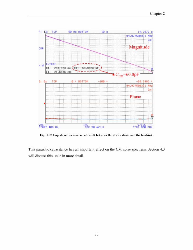
insulation material, the capacitance is measured to be 60.0pF, as indicated in the dashed-
line circle in Fig. 2.26.
Fig. 2.25 Exploded view of the device, the insulation pad and the heatsink.
Chapter 2
35
Fig. 2.26 Impedance measurement result between the device drain and the heatsink.
This parasitic capacitance has an important effect on the CM noise spectrum. Section 4.3
will discuss this issue in more detail.

Chapter 3
36
Chapter 3 EMI Simulation of the PFC Converter
This chapter presents the DM, CM and total noise simulation results for a 1KW CCM
PFC converter operating at 100KHz switching frequency. Based on the modeling and
characterization techniques described in Chapter 2, the simulated EMI noise closely
matches the measurement result in all of the DM, CM and total noise aspects. Before the
results are shown, two important issues for obtaining such good match are discussed, and
the PFC converter hardware will be briefly described.
3.1. Simulation Time Step Selection Using the modeling and characterization techniques in the medium and high frequency
ranges, a detailed simulation circuit can be obtained. A simplified version of it is shown
in Fig. 3.1.
Fig. 3.1 Detailed simulation circuit for the PFC EMI prediction (simplified).
With the simulation circuit, it is still necessary to select appropriate simulation time step,
which is an important parameter for circuit simulations, especially for the EMI
simulation.
Different simulation time steps can yield different simulation results. As can be seen from
Fig. 3.2, the simulated DM noise spectrum using the 2ns time step (top spectrum) is

Chapter 3
37
different from that using the 20ns time step (bottom spectrum). The difference occurs
mainly in the high frequency range. The magnitudes at low frequencies are almost
identical.
Fig. 3.2 DM noise simulation result comparison using time steps of 2ns and 20ns.
Generally, using a smaller simulation time step can yield more accurate simulation
waveforms. However, simulations using small time steps also require longer simulation
times and require more memory space. So the question is that what is a reasonable
simulation time step that can satisfy the demand for EMI simulation while using the
shortest simulation time and smallest amount of memory space. The answer should be
related to the high-end frequency of conducted EMI regulations, which is 30MHz. For
the 30MHz sinusoidal signal, the period is approximately 33.3ns. When the simulation
time step is 2ns, there will be at least 16 points for each period, which should be an
adequate number to represent a sinusoidal signal for one period. Therefore, the simulation
result around 2ns should be a reasonable choice and the following comparison will
Chapter 3
38
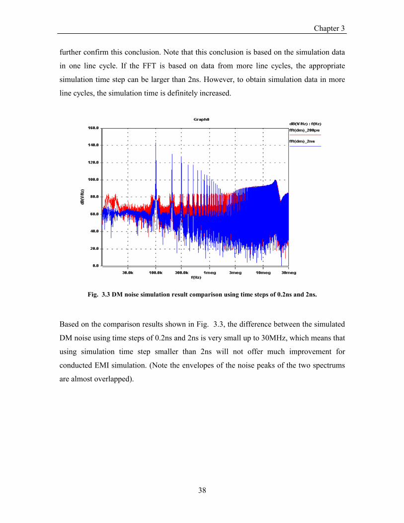
further confirm this conclusion. Note that this conclusion is based on the simulation data
in one line cycle. If the FFT is based on data from more line cycles, the appropriate
simulation time step can be larger than 2ns. However, to obtain simulation data in more
line cycles, the simulation time is definitely increased.
Fig. 3.3 DM noise simulation result comparison using time steps of 0.2ns and 2ns.
Based on the comparison results shown in Fig. 3.3, the difference between the simulated
DM noise using time steps of 0.2ns and 2ns is very small up to 30MHz, which means that
using simulation time step smaller than 2ns will not offer much improvement for
conducted EMI simulation. (Note the envelopes of the noise peaks of the two spectrums
are almost overlapped).
Chapter 3
39
3.2. Noise Separator Selection
Although the EMI standards regulate the total EMI noise, the noises can be divided into
DM noise and CM noise in order to effectively minimize each type of noise for an overall
emission suppression. The noise separator is an essential component to serve this
purpose.
Several types of noise separators have been discussed in previous literature. Nave has
several patents to build noise separators and his company provided these rejection
networks several years ago [C 1]. Current probes can also be used to measure both modes
of noise current. However, it requires a sophisticated current probe. Furthermore, for the
government regulation, the noise voltage is the concern, and it is not straightforward to
convert the measured noise current to noise voltage [C 7].
Ting Guo proposed a noise separator using power combiner/splitter [C 7]. The basic
working principle can be expressed as follows, and an example is shown in Fig. 3.4. The
noise separator for measuring the DM noise is essentially a CM rejection network. A
180° power combiner can fulfill this requirement, because this combiner can cancel two
voltages with the same phase while combining two voltages out of phase. Since the
voltage across one LISN resistor is DMCM + , and the other is DMCM − , the CM
noise will be canceled out, and the DM noise remains. Note that the output voltage will
be DM2 instead of DM2 , since the output power needs to be equal to the input
power. For a more detail derivation, see the reference [C 7].

Chapter 3
40
Fig. 3.4 Working principle of the noise separator (taking the CM rejection network as an example).
The function of the noise separator is to reject CM noise while passing the DM noise, or
to reject DM noise while passing the CM noise. Two kinds of power splitters have been
selected to serve as the noise separators in [C 7] with the Mini-circuit Company part
number ZFSCJ-2-1 and ZFSC-2-6-75. During the EMI measurement of this work, two
better noise separators are found with the Mini-circuit Company part number ZSCJ-2-2
and ZSC-2-2. Checking the noise separators’ performance with the two basic
requirements for noise separators can reveal the difference between the previous noise
separators and the new ones.
Requirement 1: Passing CM noise while rejecting DM noise, or passing DM
noise while rejecting CM noise, as illustrated in Fig. 3.4.
Requirement 2: The input impedance of ports 1 and 2 should be 50Ω when port
S is connected to 50Ω impedance.

Chapter 3
41
Since the interfaces of the ports 1 and 2 are coaxial BNC type connectors, the instruments
for measuring the input impedance of them also need to have coaxial interface. One
instrument for this measurement is the network analyzer. Network analyzers can measure
the electrical parameters such as transfer function gain, transfer function phase, reflection
coefficient r , and S-parameters.
For one port network or a single port of a multi-port network, the reflection coefficient r
is defined as the ratio of the reflected wave to the incident wave. Once the reflection
coefficient of that port is measured, the input impedance of that port, inZ , can be
calculated from the reflection coefficient r based on the following formula:
rrZZin −
+=11
0 ( 3.1 )
where the 0Z is the characteristic impedance of the measurement system, normally 50Ω
or 75Ω.
The measurement setup for measuring the reflection coefficient r is shown in Fig. 3.5.
The spectrum analyzer HP4195A launches a frequency-sweeping signal to the noise
separator. The incident wave and the reflected wave are detected by the HP41952A
transmission/reflection test set. When measuring the reflection coefficient of port 1 or
port 2, port S needs to be connected to a 50Ω standard load. The termination of the other
port is not important; one can refer to the explanation for the isolation of the noise
separator in [C 7] for the reason.

Chapter 3
42
Fig. 3.5 Measurement setup for the reflection coefficient.
Using the measurement setup in Fig. 3.5, the reflection coefficient r of ports 1 and 2 of
the noise separator can be measured. Using the previous formula rrZZin −
+=11
0 , the input
impedance of ports 1 and 2 can be obtained.
With respect to requirement 2, the measurement impedance of the previous CM rejection
network (CMRN) ZFSCJ-2-1 is shown in Fig. 3.6.

Chapter 3
43
Fig. 3.6 Input impedance measurement result of the previous noise separator.
As can be seen from Fig. 3.6, the input impedance at low frequencies is less than 30Ω,
and the phase is between 40° and 50°, while the ideal value is 50Ω and 0°. This deviation
from the ideal value will lead to a low CM rejection ratio for the noise separator. One
experiment can verify that the CM rejection ratio is not high enough at 100KHz.
Fig. 3.7 Measurement setup for the CM rejection ratio
In this measurement setup, voltages VCM1 and VCM2 are the same output voltages of the
signal generator, so they can be considered as CM voltage. And they are connected to the
output power ports of the two LISN. The voltage across the two 50Ω resistances in the
LISN are connected to ports 1 and 2 of the CMRN. Note that these two 50Ω resistances

Chapter 3
44
are not real resistors. They are reflected from port S when it is connected to 50Ω load.
The voltage ratio between the output of the CMRN and the VCM1/VCM2 will reflect the
performance of the CMRN. Using 100KHz sinusoidal excitation as VCM1 and VCM2, the
actual measurement results are shown in Fig. 3.8.
Fig. 3.8 Measurement result of the CM rejection ratio of the previous CMRN at 100KHz.
According to Fig. 3.8, the rejection ratio at 100KHz is only 22dB, which is not good
enough for the purpose of rejection. The reason is that the working frequency range of
this particular power splitter, ZFSCJ-2-1, is from 1MHz to 500MHz [C 7], while the
conducted EMI regulation frequency range is from 150KHz to 30MHz. After searching
the catalog of the same company, Mini-circuit, a new power splitter is found and it can
better serve as a DM noise measurement tool. The part number is ZSCJ-2-2, and one
picture of it is shown in Fig. 3.9.
Chapter 3
45
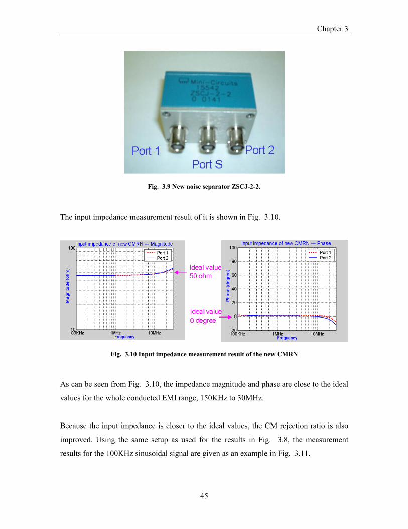
Fig. 3.9 New noise separator ZSCJ-2-2.
The input impedance measurement result of it is shown in Fig. 3.10.
Fig. 3.10 Input impedance measurement result of the new CMRN
As can be seen from Fig. 3.10, the impedance magnitude and phase are close to the ideal
values for the whole conducted EMI range, 150KHz to 30MHz.
Because the input impedance is closer to the ideal values, the CM rejection ratio is also
improved. Using the same setup as used for the results in Fig. 3.8, the measurement
results for the 100KHz sinusoidal signal are given as an example in Fig. 3.11.

Chapter 3
46
Fig. 3.11 CM rejection ratio of the new CMRN at 100KHz.
As can be seen from Fig. 3.11, the CM rejection ratio of the noise separator ZSCJ-2-2 at
100KHz is 50dB, which is greatly improved over the previous CMRN.
In addition to the CM rejection ratio comparison at 100KHz, the CM rejection ratios of
these two noise separators are compared over a wide frequency range, from 200KHz to
15MHz (the highest frequency of the signal generator HP33120A). The result is shown in
Table 3-1.
Table 3-1 CM rejection ratio comparison of the previous CMRN and the new CMRN.
CM Rejection Ratio (dB) Previous CMRN
(ZFSCJ-2-1)
New CMRN
(ZSCJ-2-2)
100KHz 22.1 50.5
200KHz 42.0 57.8
400KHz 55.1 60.7
600KHz 63.7 62.1
800KHz 65.0 62.0
1MHz 64.3 61.8
2MHz 54.1 55.4
4MHz 45.3 48.1

Chapter 3
47
6MHz 41.9 44.7
8MHz 40.2 42.9
10MHz 37.7 40.1
15MHz 34.1 35.4
As can be seen from Table 3-1, the performance of the new CMRN is better than the
previous CMRN at the frequencies below 400KHz. There are two reasons for this
phenomenon. The first one is that the input impedance of port 1 and port 2 of the new
CMRN is closer to the ideal value. The second reason is that the input impedance of port
1 is slightly different from that of port 2 for the previous CMRN, while the input
impedance of port 1 is almost identical to that of port 2 of the new CMRN at the
frequencies below 400KHz.

Chapter 3
48
3.3. Hardware Description The hardware for the measurement and simulation is a 1KW PFC converter operating in
CCM. The circuit diagram and a picture of the converter are shown in Fig. 1.1 and Fig.
2.1, respectively.
The MOSFET in Fig. 1.1 is actually realized by paralleling two MOSFETs. They are the
product from Infineon Corporation; the part number for the MOSFETs is SPW20N60C3.
The diode is also a product from Infineon Corporation, and its part number is SDT06S60.
The diode bridge at the input side of the PFC converter is GBJ2006 from Diodes
Corporation.
The core for the inductor is the 77083A core from Magnetics Corporation. And the 49-
turn winding employs AWG16 wire. One 330uF electrolytic capacitor is used as the
output bulk capacitor, and ceramic capacitors are paralleled with the bulk capacitor to
filter out the high frequency noise at the output side and suppress the voltage stress of the
device. These ceramic capacitors need to be located as close as possible to the MOSFET
and the diodes.
The controller is ML4821 from Fairchild Corporation. This chip can implement the
average current mode control for the PFC circuit.
The active load is widely used in industry and laboratories for power converter testing.
However, it may not be a good choice for the EMI measurement because this kind of load
will introduce more coupling and propagation paths in the EMI test environment, thus
complicating the scenario. A resistor bank should be used for EMI measurement and it is
the load for the hardware in this thesis.

Chapter 3
49
3.4. EMI Noise Prediction for the PFC Converter
Based on all of the efforts expended for modeling and characterization in the medium and
high frequency ranges, careful selection of the simulation time step, and improvement in
the measurement setup, the conducted EMI results from the Saber simulation and the
spectrum analyzer measurement are ready to compare. The conducted EMI of the PFC
converter is measured using the HP4195A spectrum/network analyzer and the afore-
mentioned noise separators.
The comparison is performed for all of the DM, CM and total noise, as shown in Fig.
3.12, Fig. 3.13.and Fig. 3.14.
Fig. 3.12 DM noise comparison of the PFC converter.

Chapter 3
50
Fig. 3.13 CM noise comparison of the PFC converter.
Fig. 3.14 Total noise comparison of the PFC converter.

Chapter 3
51
As can be seen from the comparisons for the DM, CM and total noise, the modeling and
characterization techniques in components level, device level, module level and system
layout level are effective for predicting the conducted EMI noise of the PFC circuit.
The measurement setup for the DM or CM noise is shown in Fig. 3.15. When measuring
the total noise, the noise separator is not used. One LISN is terminated with 50Ω load,
and another LISN is connected to the input port of the spectrum analyzer.
Fig. 3.15 Measurement setup for the DM or CM noise.

Chapter 4
52
Chapter 4 DM/CM Loop Models and the Effects of Circuit Components on EMI
From the comparison result in Section 3.4, the simulated DM, CM and total noise of the
CCM PFC converter accurately predicts the measured EMI noise. This is a desired result
and is of great help for the EMI filter design. However, this result itself does not provide
a clear explanation about the noise generation and propagation mechanism. In this
chapter, further analysis will be performed in a systematic way to explore this problem.
The analysis will begin with the derivation of the DM loop and CM loop models, which
will be proved as the major mechanism for the PFC EMI generation and propagation.
4.1. DM Loop and CM Loop Models
The circuit diagram of the CCM PFC converter and the line impedance stabilization
network (LISN) is shown in Fig. 4.1. Because the parasitic capacitance between the
MOSFET drain and the ground, CCM, provides a path for the noise current to flow, it is
also included in the circuit diagram.
Fig. 4.1 Circuit diagram of PFC converter and the LISN.

Chapter 4
53
In the PFC circuit, the MOSFET is the component that is controlled to switch in order to
realize the PFC function. The voltage across its drain and source, VDS, pulsates between
0V and the output DC voltage, which is 380V to 400V in this case, so this voltage is
considered to be the noise source in the PFC circuit. For this noise source, there are two
mechanisms to propagate its noise energy. One will be named the DM loop and the other
will be named the CM loop. Because the DM loop and the CM loop are new terms and
they are different from the generally accepted terms DM noise and CM noise, the
definitions of these four terms need to be clarified before further discussion.
Definitions of the terms:
DM loop: One of the two conducted EMI noise generation and propagation mechanisms
for CCM PFC converters. In this mechanism, the noise current will flow from the
MOSFET, through the LISN, the PFC inductor and finally back to MOSFET to complete
a loop.
CM loop: One of the two conducted EMI noise generation and propagation mechanisms
for CCM PFC converters. In this mechanism, the noise current will flow from the
MOSFET, through the parasitic capacitance between the device and the heat sink (CCM),
the LISN, finally back to the MOSFET to complete a loop.
The DM noise (VDM) and the CM noise (VCM) are generally accepted terms in the
literatures written about EMI analysis [C 6].
DM noise: Referring to Fig. 4.1, V1 and V2 are the voltages across the two LISN
resistances with respect to the ground. The DM noise VDM is defined as
221 VVVDM
−= . ( 4.1 )
CM noise: Referring to Fig. 4.1, the CM noise VCM is defined as

Chapter 4
54
221 VVVCM
+= . ( 4.2 )
One point that needs to be clarified is that in normal cases, DM noise comes mainly from
DM loop and CM noise comes mainly from CM loop. However, in certain circumstances,
the CM loop can also contribute to the DM noise. One example is the mixed-mode noise
discussed in [C 11]. For the CCM PFC circuit shown in Fig. 4.1, the CM loop also
contributes to the DM noise. Even with a capacitor added at the output side of the diode
bridge, if the input wires are in unbalanced condition, the CM loop still contributes to the
DM noise as discussed in Section 4.5. As long as the two LISN resistors are identical, the
DM loop should not contribute to the CM noise.
4.1.1. DM Loop Model
Since this is a CCM PFC circuit, it is reasonable to assume that there will be two diodes
conducting the current in the diode bridge at any time; either D1 and D4 or D2 and D3.
And the high frequency noise voltage of the VDS will cause a noise current flow through
D1 and D4 or D2 and D3, as shown in Fig. 4.2 and Fig. 4.3, respectively.
Fig. 4.2 DM loop model when D1 and D4 conduct.

Chapter 4
55
Fig. 4.3 DM loop model when D2 and D3 conduct.
The noise loops shown in Fig. 4.2 and Fig. 4.3 are basically the same mechanism, which
is called the DM loop in this thesis. For either one of these two cases, the DM loop can
be simplified as shown in Fig. 4.4.
Fig. 4.4 Simplified DM loop model
From the simplified DM loop model shown in Fig. 4.4, the PFC inductor is a component
that significantly affects the noise level in the DM loop. The waveform of the noise
source also affects the noise level.

Chapter 4
56
4.1.2. CM Loop Model
Depending on whether D1 and D4 or D2 and D3 conduct the line frequency current, there
are also two cases for another noise propagation mechanism.
When D1 and D4 conduct the current, there will be noise current flowing through the
MOSFET, the parasitic capacitance CCM, one 50Ω resistor in the LISN, D4 and then
flowing back to the MOSFET to complete one loop. This situation is shown in Fig. 4.5.
D2 and D3 are in OFF state so they don’t conduct noise current. Although D1 is ON, the
noise through it will be limited to a negligible level since the impedance of the PFC
inductor is high.
Fig. 4.5 CM loop model when D1 and D4 conduct.
Another case is shown in Fig. 4.6. When D2 and D3 conduct the current, the noise flows
through the MOSFET, the parasitic capacitance CCM, the other 50Ω resistor in the LISN,
D2 and then goes back to the MOSFET to complete one loop.

Chapter 4
57
Fig. 4.6 CM loop model when D2 and D3 conduct.
For either one of these two cases, the CM loop can be simplified as shown in Fig. 4.7.
The waveform of the noise source and the value of the CCM will have great impact on the
noise in the CM loop. Actually, if the parasitic inductance of the trace and the ground
connection is large, it should also be taken into account in the CM loop.
Fig. 4.7 Simplified CM loop model.
One point that needs to be clarified is that the noise current in the CM loop induces
voltage drop only in one of the two LISN resistors; either V1 is the voltage drop and V2
equals to zero, or V2 is the voltage drop and V1 equals to zero. Therefore V1 and V2 are
not the same in this case. According to the equation 2
21 VVVDM−= , as long as V1 is not

Chapter 4
58
equal to V2, it will result in DM noise. This is the reason for that the CM loop contributes
to the DM noise.
In the following sections, verification of the DM and CM loop models are performed in
both simulation and measurement. From the simplified DM and CM loop models shown
in Fig. 4.4 and Fig. 4.7, the factors that have great impact on the noise level are the PFC
inductor, the CCM value and the VDS waveform. So, parametric studies of these factors
will be performed to verify the noise loop models.

Chapter 4
59
4.2. The Effect of the PFC Inductor on DM Noise As described in the previous section, the PFC inductor plays an important role in the DM
loop model of the PFC circuit. In this section, two inductors with different high frequency
characteristics are used for parametric study and verification of the DM loop.
The impedance magnitude characteristic of the first inductor, inductor 1, is shown in Fig.
4.8.
Fig. 4.8 Impedance magnitude of inductor 1.
The frequency range of the measurement is from 10KHz to 30MHz. In this frequency
range, there are two peaks (f1 and f3) and one valley (f2) in the magnitude curve. An
equivalent circuit can be created based on the method descried in Section 2.2.1.Using that
equivalent circuit in the Saber simulation, the simulated DM noise is shown in Fig. 4.9.

Chapter 4
60
Fig. 4.9 Simulated DM noise using the high order inductor model for inductor 1.
As can be seen from Fig. 4.9, the impedance valley and peaks show their effect in the
DM noise spectrum in the corresponding frequencies. Using the DM loop model in Fig.
4.4, it is easy to explain this phenomenon. From the measurement result in Fig. 4.8, the
impedance magnitude of the PFC inductor is higher than the resistance of the LISN
resistor (50Ω×2), which means the noise current will be greatly affected by the
impedance magnitude of the PFC inductor. So, at the impedance peak frequencies, such
as f1 or f3, the noise current in the DM loop is small; thus the DM noise voltage is small.
On the other hand, at the impedance valley frequencies, such as f2, the noise current in
the DM loop is large; so that the DM noise voltage at that frequency is large. The
simulation result in Fig. 4.9 is verified by the measured DM noise, as shown in Fig.
4.10.

Chapter 4
61
Fig. 4.10 Verification of the DM noise simulation result using inductor 1.
In order to verify the DM loop, another PFC inductor, inductor 2, is wound with a
different pattern so that the high frequency characteristic is different from that of inductor
1. The winding of inductor 2 is concentrated around 1/3 of the toroidal core, instead of
distributing the winding evenly around the whole toroidal core, as was the case for
inductor 1.
Fig. 4.11 Impedance magnitude of inductor 2.

Chapter 4
62
As can be seen from Fig. 4.11, the magnitude curve of inductor 2 also has two peaks (f4
and f6) and one valley (f5) up to 30MHz. However, because the winding patterns are
different, the peak and valley frequencies of inductor 2 are different from those of
inductor 1, as listed in Table 4-1.
Table 4-1 Comparison of the frequencies of the impedance peaks and valleys of the two inductors.
First Peak First Valley Second Peak
Inductor 1 f1=2.4MHz f2=17.8MHz f3=23.7MHz
Inductor 2 f4=2.0MHz f5=10.7MHz f6=11.6MHz
Fig. 4.12 Verification of the DM noise simulation result using inductor 2.
As expected, the simulated DM noise for inductor 2 also shows the effect of the
impedance peaks at f4 and f6, as well as the effect of impedance valley at f5. And the
measured DM noise verifies the simulation result, as shown in Fig. 4.12.

Chapter 4
63
4.3. The Effect of the Parasitic Capacitance CCM on the CM Noise
As described in Section 4.1.2, the parasitic capacitance between the device and the
heatsink, CCM, plays an important role in the CM loop model of the PFC circuit. In this
section, parametric study of the CCM value is performed to verify the CM loop model.
The value of the CCM is in the range of tens to hundreds of pF . So, the impedance
magnitude of this capacitance will also be higher than the resistance of the LISN resistor
in the frequency range lower than 30MHz. The smaller the CCM value, the higher the
impedance magnitude of this capacitance, and based on the CM loop model shown in Fig.
4.7, a smaller noise current in the CM loop will also result. To verify this conclusion, two
kinds of insulation pads are used in experiments. These two insulation pads are inserted
between the device and the heatsink of two structures. Based on the impedance
measurement results shown in Fig. 4.13, for insulation pad 1, the CCM value is 22.7pF.
Fig. 4.13 Insulation pad 1 and the impedance measurement result of CCM with pad 1.

Chapter 4
64
For insulation pad 2, the CCM value is measured to be 60.0pF, as shown in Fig. 4.14.
Fig. 4.14 Insulation pad 2 and the impedance measurement result of CCM with pad 2.
Considering the CM loop model shown in Fig. 4.7, it is expected that when different
insulation pads are used, the CM noise level will be different due to the difference in CCM
values. The CM noise simulation and measurement results in Fig. 4.15 also comply this
expectation.
Fig. 4.15 CM noise simulation and measurement results using different insulation materials.

Chapter 4
65
As can be seen from Fig. 4.15, when insulation material 1 is used as the pad, the
simulated CM noise is about 6dB lower than for insulation material 2. Measurement
results confirm the simulation results.
Chapter 4
66
4.4. The Effect of the VDS Rising and Falling Times on DM and CM Noise
In Sections 4.2 and 4.3, the effects of the PFC inductor and the parasitic capacitance CCM
are studied. It is shown that the inductor is a critical factor in the DM loop, and that the
CCM value is a critical factor in the CM loop. In addition to these two factors, the noise
source, VDS voltage, should also have an effect on the noise spectrum. In this section, the
effect of VDS voltage will be studied.
Since the VDS voltage is the noise source in both the DM and CM loops, its effect should
apply to both loops.
4.4.1. Frequency Spectrum of the VDS Voltage
Since in the real measurement the ringing frequencies at the turn-on and turn-off
transients are found to be higher than 30MHz for this PFC circuit, only the effects of the
rising time (tr) and falling time (tf) will be studied to determine the impact of noise source
on the noise spectrum.
A measured VDS waveform is shown in Fig. 4.16. To simplify the discussion, the effect
of the ringing at the turn-on and turn-off transients is neglected for the afore-mentioned
reason. Therefore, the measurement waveform in Fig. 4.16 can be approximated with a
trapezoidal waveform, such as the one in Fig. 4.17.
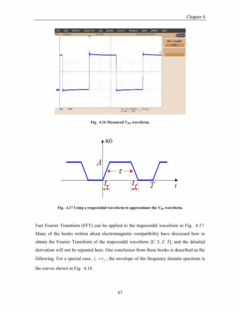
Chapter 4
67
Fig. 4.16 Measured VDS waveform.
Fig. 4.17 Using a trapezoidal waveform to approximate the VDS waveform.
Fast Fourier Transform (FFT) can be applied to the trapezoidal waveform in Fig. 4.17.
Many of the books written about electromagnetic compatibility have discussed how to
obtain the Fourier Transform of the trapezoidal waveform [C 3, C 5], and the detailed
derivation will not be repeated here. One conclusion from these books is described as the
following. For a special case, fr tt = , the envelope of the frequency domain spectrum is
the curves shown in Fig. 4.18.

Chapter 4
68
Fig. 4.18 The envelope of the frequency domain spectrum of the trapezoidal waveform.
The amplitude of the trapezoidal waveform in Fig. 4.17 is denoted as A . The period is
denoted as T , and the positive pulse width is denoted as τ . The rising time and the
falling time are denoted as rt and ft , respectively. As can be seen from Fig. 4.18, there
are two corner frequencies in the FFT spectrum. The first one, 1cf , is inversely
proportional to the pulse width, τ , and the second one, 2cf , is inversely proportional to
the rising time rt and falling time ft . The smaller the rt and ft , the higher the 2cf .
The pulse width, τ , is determined by the control law in order to fulfill the power factor
correction function. Therefore, the first corner frequency 1cf will be fixed as long as the
control law is fixed. However, the second corner frequency, 2cf , will not be fixed, since
the rt and ft are related to circuit parameters such as the gate resistors. Using different
gate resistors will result in different switching speeds. Generally, when the gate resistor is
smaller, the switching speed will be faster, and thus the switching loss can be reduced.
One question is that when the rising time and falling time are reduced, how will it affect
the conducted EMI noise?

Chapter 4
69
From the equation of 2cf ,
rc tf
⋅=
π1
2 . ( 4.3 )
the rising/falling time corresponding to the 30MHz frequency is 10.6ns. Based on this
calculation, the following conclusions can be drawn.
1) Given two gate resistors, if tr=tf<10.6ns for both of them, then no difference in
the DM noise or the CM noise should be observed up to 30MHz
2) Given two gate resistors, if tr=tf<10.6ns for one case and tr=tf>10.6ns for the
other case, the difference in the DM noise and the CM noise should only be seen
above the smaller fc2
One point that must be clarified is that all the previous discussion in this section is based
on the assumption fr tt = . This assumption is not valid for the real circuit. The real case
is that the ft of the VDS waveform is fixed, but the rt changes. However, even the
smallest rt is still several times larger than the falling time ft .
Simulation results reveal that when one of the turn-on and turn-off transients is ten times
larger than the other one, the final frequency spectrum of the VDS voltage will behave
more like that of both turn-on and turn-off transients switch with the smaller one, ft in
this case. So the previous two conclusions need to be modified as follows.
1) Given two gate resistors, if tf<10.6ns for both of them, then no difference in the
DM noise or the CM noise should be observed up to 30MHz
2) Given two gate resistors, if tf<10.6ns for one case and tf>10.6ns for the other
case, the difference in the DM noise and the CM noise should only be seen above
the smaller fc2

Chapter 4
70
The following measurement result of the DM noise and the CM noise will verify these
two conclusions.
4.4.2. The Effect of tr and tf on DM noise
The discussion in Section 4.4.1 reveals that given two gate resistors, if the tf<10.6ns for
both of them, then no difference in the DM noise should be observed up to 30MHz. The
results from the following two experiments can verify this statement.
In these two experiments, two different gate resistors are used. One is a 3Ω resistor and
the other one is a 15Ω resistor.
For the 3Ω resistor, the VDS falling time tf is measured to be 7.8ns, as shown at the upper-
right corner of the measurement waveform in Fig. 4.19. In another experiment, the VDS
falling time tf is measured to be 10.2ns with the 15Ω gate resistor. This value can be seen
in the dashed-line circle at the upper-right corner of Fig. 4.20.

Chapter 4
71
Fig. 4.19 VDS falling time Tf measurement result with the 3ΩΩΩΩ gate resistor.
Fig. 4.20 VDS falling time Tf measurement result with the 15ΩΩΩΩ gate resistor.

Chapter 4
72
For both of these cases, the VDS falling times are less than 10.6ns. Based on the FFT
analysis of the VDS waveform and the DM loop model, no difference in the DM noise
should be observed up to 30MHz. The measured DM noise with the 3Ω gate resistor is
shown in Fig. 4.21. The DM noise measurement result for the 15Ω gate resistor is shown
in Fig. 4.22.
Fig. 4.21 DM noise measurement result with the 3ΩΩΩΩ gate resistor.
Fig. 4.22 DM noise measurement result with the 15ΩΩΩΩ gate resistor.

Chapter 4
73
From the measurement results shown in Fig. 4.21 and Fig. 4.22, the DM noise shapes
and levels for these two gate resistors are very similar. In Fig. 4.23 they are plotted in
one figure, which shows that the difference between these two waveforms is very small.
So the first conclusion relating to the effect of tr and tf is verified for DM noise.
Fig. 4.23 DM noise measurement result comparison for the case with the 15ΩΩΩΩ gate resistor and the
case with the 3ΩΩΩΩ gate resistor.
To verify the second conclusion relating to the effect of tr and tf on DM noise, one more
experiment is needed. In the third experiment, the gate resistor is a large one (51Ω) so
that the scenario of the second conclusion can be realized. Using the 51Ω gate resistor,
the VDS falling time is measured to be 29.6ns, as Fig. 4.24 indicates. Based on the second
conclusion, the DM noise of the third experiment will be different from the DM noise in
the previous two experiments in high frequencies.

Chapter 4
74
Fig. 4.24 DM noise measurement result with the 51ΩΩΩΩ gate resistor.
For the 15Ω gate resistor, the falling time tf is 10.2ns. According to the previous analysis,
the second corner frequency of the VDS voltage spectrum 2cf can be approximately
calculated as MHzt
fohmf
c 2.311
15,2 =≈
π.
Using a similar method, with the 51Ω gate resistor, the 2cf is calculated as
MHzt
fohmf
c 8.101
51,2 =≈
π. The implication of the difference of these two values of 2cf is
that only in the frequency range higher than 10.8MHz will there be difference for the VDS
voltage spectrum of these two cases. Because other circuit parameters are identical, the
measured DM noise also should only have difference in the frequency range higher than
10.8MHz.
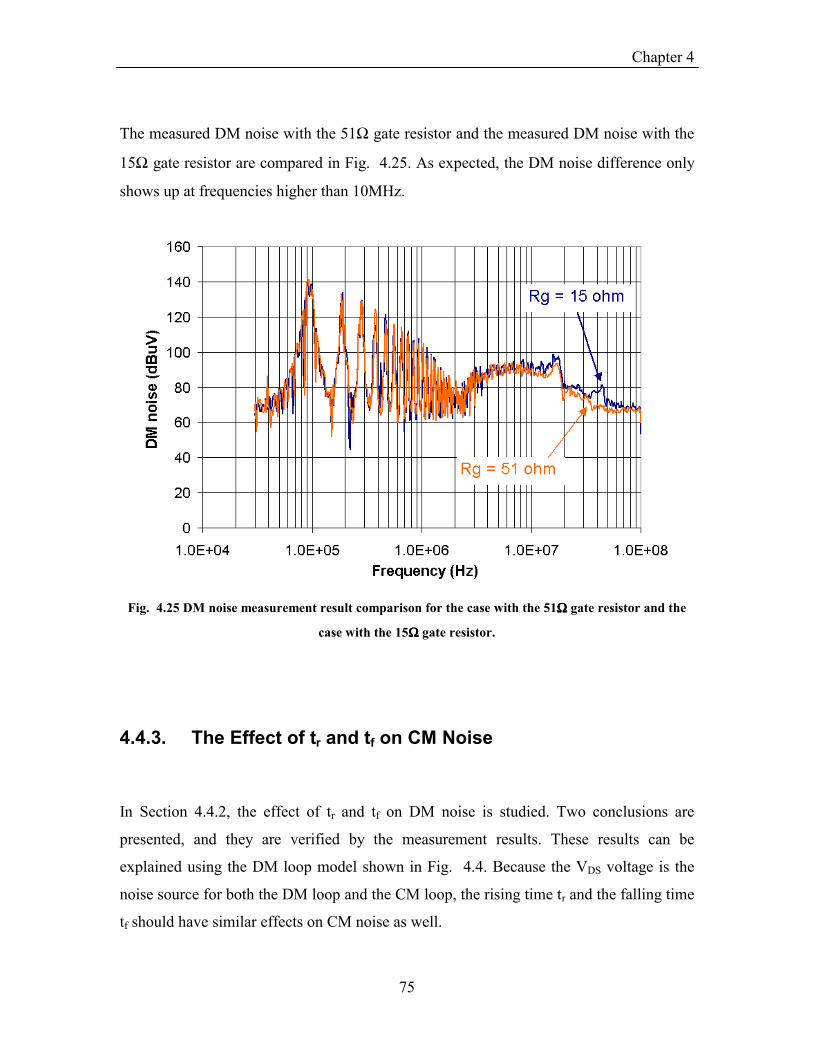
Chapter 4
75
The measured DM noise with the 51Ω gate resistor and the measured DM noise with the
15Ω gate resistor are compared in Fig. 4.25. As expected, the DM noise difference only
shows up at frequencies higher than 10MHz.
Fig. 4.25 DM noise measurement result comparison for the case with the 51ΩΩΩΩ gate resistor and the
case with the 15ΩΩΩΩ gate resistor.
4.4.3. The Effect of tr and tf on CM Noise
In Section 4.4.2, the effect of tr and tf on DM noise is studied. Two conclusions are
presented, and they are verified by the measurement results. These results can be
explained using the DM loop model shown in Fig. 4.4. Because the VDS voltage is the
noise source for both the DM loop and the CM loop, the rising time tr and the falling time
tf should have similar effects on CM noise as well.

Chapter 4
76
Fig. 4.26 CM noise measurement result with the 3ΩΩΩΩ gate resistor.
Fig. 4.27 CM noise measurement result with the 15ΩΩΩΩ gate resistor.

Chapter 4
77
In the previous three experiments (the 3Ω, 15Ω and 51Ω gate resistors), CM noise is also
measured. The measurement results for the case of the 3Ω gate resistor is shown in Fig.
4.26 and that for the case of the 15Ω gate resistor is shown in Fig. 4.27. The noise levels
and noise shapes are very similar in these two figures, and the comparison given in Fig.
4.28 shows that they are essentially not very different, as was predicted by the first
conclusion in Section 4.4.1.
Fig. 4.28 CM noise measurement result comparison for the case with the 3ΩΩΩΩ gate resistor and the
case with the 15ΩΩΩΩ gate resistor.
The second conclusion in Section 4.4.1 can also be verified by the CM noise
measurement result comparison of the case with the 15Ω gate resistor and the case with
the 51Ω gate resistor. As calculated in section 4.4.2, the 2cf for the 15Ω gate resistor
case is 31.2MHz and that for the 51Ω gate resistor case is 10.8MHz. As can be seen from
Fig. 4.29, the difference in these two CM noise measurement results can only be seen at
frequencies higher than 10.8MHz.
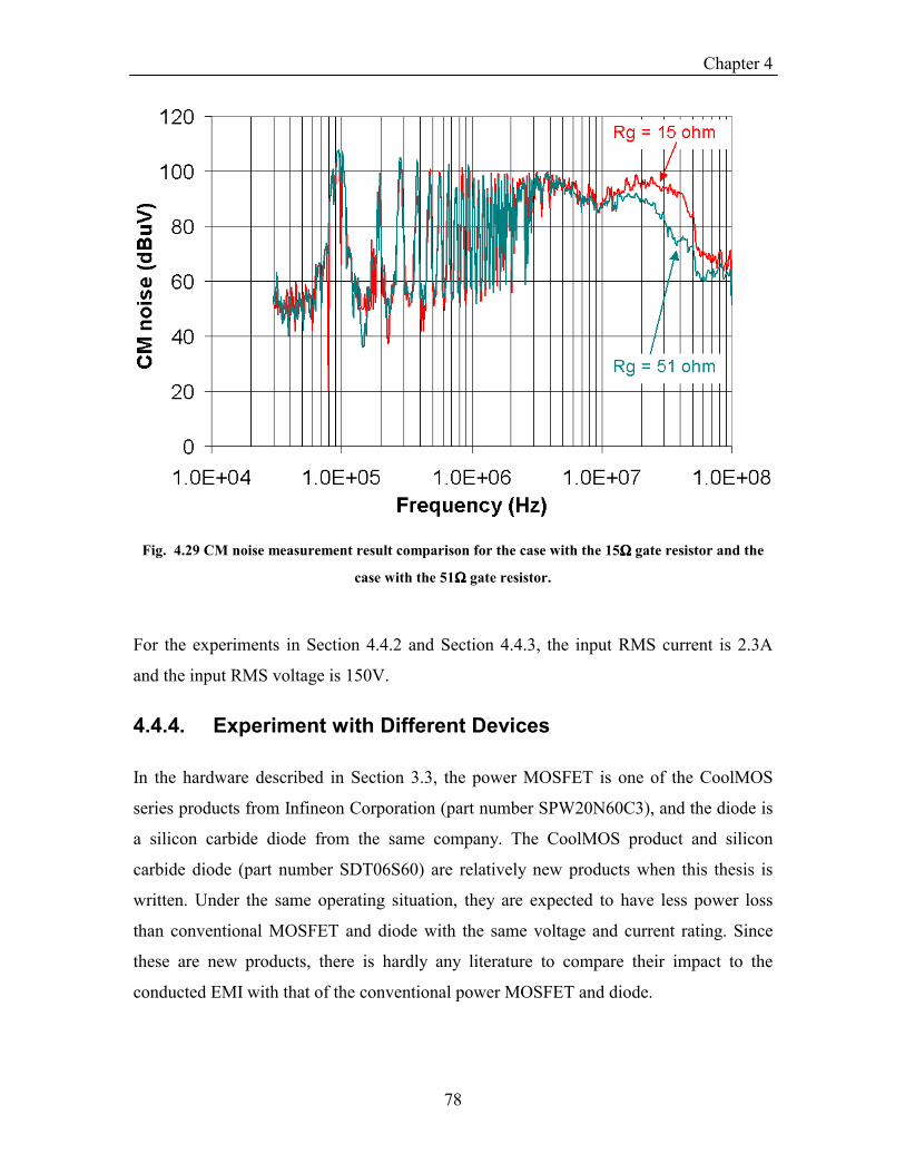
Chapter 4
78
Fig. 4.29 CM noise measurement result comparison for the case with the 15ΩΩΩΩ gate resistor and the
case with the 51ΩΩΩΩ gate resistor.
For the experiments in Section 4.4.2 and Section 4.4.3, the input RMS current is 2.3A
and the input RMS voltage is 150V.
4.4.4. Experiment with Different Devices
In the hardware described in Section 3.3, the power MOSFET is one of the CoolMOS
series products from Infineon Corporation (part number SPW20N60C3), and the diode is
a silicon carbide diode from the same company. The CoolMOS product and silicon
carbide diode (part number SDT06S60) are relatively new products when this thesis is
written. Under the same operating situation, they are expected to have less power loss
than conventional MOSFET and diode with the same voltage and current rating. Since
these are new products, there is hardly any literature to compare their impact to the
conducted EMI with that of the conventional power MOSFET and diode.

Chapter 4
79
For this reason, the experiments of conducted EMI comparison with different devices are
performed in this thesis. IRFP460A and RHRP1560 are selected as conventional
MOSFET and diode, respectively. The results are given in the following paragraphs.
Two gate resistors are experimented with. When the gate resistor is 15Ω, the falling time
of the IRFP460A VDS waveform is measured to be 13.9ns as shown in Fig. 4.30. The
second corner frequency corresponding to 13.9ns is 22.9MHz.
Fig. 4.30 Falling time of the IRFP460A VDS waveform with Rg=15ohm.
Under the same situation, the falling time of the SPW20N60C3 VDS waveform is
measured to be 9.6ns as shown in Fig. 4.31. The second corner frequency corresponding
to 9.6ns is 33.2MHz.

Chapter 4
80
Fig. 4.31 Falling time of the SPW20N60C3 VDS waveform with Rg=15ohm.
Based on the two conclusions in Section 4.4.1, the difference should only be seen above
the smaller 2cf , 22.9MHz. However, from the comparison of the measured DM noise of
these two cases in Fig. 4.32, the difference between these two DM noise is negligible up
to 30MHz. The reason may be that the falling edge of IRFP460A VDS waveform shown
in Fig. 4.30 is not suitable to be approximated with trapezoidal waveform. The later part
of the VDS falling edge is steeper than the former part, so the actual second corner
frequency may be still higher than 22.9MHz.
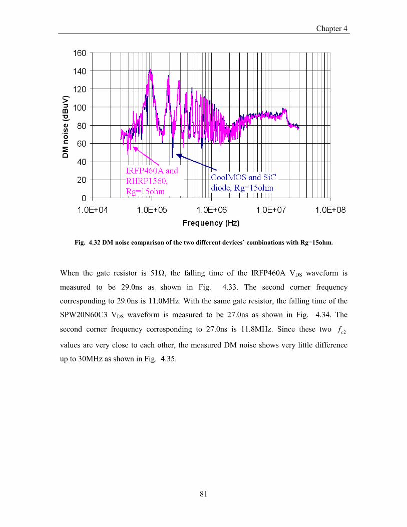
Chapter 4
81
Fig. 4.32 DM noise comparison of the two different devices’ combinations with Rg=15ohm.
When the gate resistor is 51Ω, the falling time of the IRFP460A VDS waveform is
measured to be 29.0ns as shown in Fig. 4.33. The second corner frequency
corresponding to 29.0ns is 11.0MHz. With the same gate resistor, the falling time of the
SPW20N60C3 VDS waveform is measured to be 27.0ns as shown in Fig. 4.34. The
second corner frequency corresponding to 27.0ns is 11.8MHz. Since these two 2cf
values are very close to each other, the measured DM noise shows very little difference
up to 30MHz as shown in Fig. 4.35.

Chapter 4
82
Fig. 4.33 Falling time of the IRFP460A VDS waveform with Rg=51ohm.
Fig. 4.34 Falling time of the SPW20N60C3 VDS waveform with Rg=51ohm.

Chapter 4
83
Fig. 4.35 DM noise comparison of the two different devices’ combinations with Rg=51ohm.
Based on the comparison results in this section, for these two kinds of devices’
combinations, the falling time is very close to each other when using the same gate
resistors. Therefore, the measured DM noise shows very little difference in the frequency
range specified by the conducted EMI standards. Based on the fact that DM loop and CM
loop share the same noise source, similar results should be seen for the CM noise.
However, these two sets of experiments are still not enough for drawing a general
conclusion. For other devices’ combinations, one needs to check the two conclusions in
Section 4.4.1 to analyze their effect on the conducted EMI noise.
For the experiments in Section 4.4.4, the input RMS current is 3.3A and the input RMS
voltage is 150V.

Chapter 4
84
4.5. The Effect of the Input Wires and Crec
Adding a high frequency capacitor, Crec, at the output side of the diode bridge is a
common practice for PFC circuits, as shown in Fig. 4.36. This capacitor brings two
advantages to the circuit. The first advantage is that the DM noise can be attenuated to a
lower level with Crec. The second advantage is that the voltage waveform at the output
side of the diode bridge can be filtered better so that it is more suitable to serve as the
reference waveform for the control circuit.
Fig. 4.36 The PFC circuit diagram with a capacitor Crec at the output side of the diode bridge.
With Crec in the circuit, the DM and CM noise loops will change, and the input wires
between the LISN and the diode bridge may affect the EMI noise. It is found that the
balance/unbalance configuration of the input wires will significantly affect DM noise.
This phenomenon can be explained following the DM loop and CM loop analysis method
in section 4.1.
With balanced input wires, the DM loop model is changed to the one shown in Fig. 4.37.
Note that input wires 1 and 2 have equal length. With Crec, most of the high frequency
noise in the DM loop will be bypassed by the Crec. Only a small amount of the high
frequency noise flows through the LISN resistors. The dotted arrows in Fig. 4.37

Chapter 4
85
represent the noise current in the DM loop, and the weight of the arrows indicates the
relative amplitude of the noise current.
Fig. 4.37 DM loop with balanced input wires.
The CM loop model for the case of balanced input wires is shown in Fig. 4.38. Because
the Crec provides a low impedance path, the noise current will flow through both input
wires 1 and 2. Since the two input wires are balanced, the noise current will be equally
distributed in the two paths. So the voltages across the two LISN resistors have identical
amplitudes and phases. Considering the equation for DM noise calculation,
221 VVVDM
−= ( 4.4 )
it can be concluded that the noise currents in the CM loop will not contribute to the DM
noise in this case. The final DM noise will result only from the noise current in the DM
loop that is shown in Fig. 4.37.

Chapter 4
86
Fig. 4.38 CM loop with balanced input wires.
The DM loop with unbalanced input wires is shown in Fig. 4.39. Note that the length of
input wire 1 is different from that of input wire 2. One can see that the noise current
distribution is almost the same as the pattern shown in Fig. 4.37. The Crec will bypass
most of the noise current in the DM loop, and only a small amount of it will flow through
the LISN resistor to contribute to the final DM noise.
Fig. 4.39 DM loop with unbalanced input wires.
The CM loop with unbalanced input wires is shown in Fig. 4.40. Since input wires 1 and
2 have different length, they will also have different impedances. For a wire inductance
larger than 100nH, which is the normal case, the impedance of the wire in the MHz range
will be comparable to the LISN resistor value (50Ω). So, the unbalanced input wires will
lead to different impedances in the two paths, and therefore the noise current in the two
paths will not be equal, as indicated by the dotted arrows in Fig. 4.40.

Chapter 4
87
As long as the noise current flowing through the two LISN resistors are different, they
will lead to different voltage drops across the two LISN resistors, therefore 21 VV ≠ .
Considering the equation 2
21 VVVDM−= , now the CM loop will have an effect on the
final DM noise. This is different from the situation in which the input wires are balanced.
Fig. 4.40 CM loop with unbalanced input wires.
To verify the previous discussion, two experiments are performed. One is with balanced
input wires (4 inches and 4 inches) and the other case is with unbalanced input wires (4
inches and 24 inches). The measurement setup and the final DM noise measurement
results are shown in Fig. 4.41.

Chapter 4
88
Fig. 4.41 Measurement setup and the DM noise measurement results comparison for the balanced
and unbalanced input wires.
As can be see from Fig. 4.41, the balanced/unbalanced input wires will impact the final
DM noise measurement result. Although in the normal case, balanced input wires will
naturally be used, the discussion in this section still serves as another proof supporting
the DM loop and CM loop analysis method proposed for the PFC EMI.

Conclusions and Future Work
89
Conclusions and Future Work
In this thesis, the topic of the conducted EMI prediction for the CCM PFC converter is
investigated.
Modeling and characterization techniques in the medium and high frequency ranges are
developed to model the PFC inductor, the capacitors, the parasitic parameters within an
IPEM, the layout parasitic inductance, and also the parasitic capacitance between the
device drain and the heatsink. Based on the work of other colleagues, the accuracy of the
device models are also verified.
Based on the modeling and characterization techniques, a detailed simulation circuit is
constructed to perform the EMI simulation. Up to 30MHz, the simulated DM, CM and
total noise levels closely match with the noise levels measured using a spectrum analyzer.
The issues for simulation time step size and noise separator selection are discussed, and
appropriate choices are proposed.
The discussion of this topic is led into a deeper level by the analysis of the DM loop and
CM loop models for the PFC EMI. With the DM and CM loop models, many of the
phenomena related to the PFC conducted EMI can be explained, such as the envelope of
the DM and CM noise spectrum. Parametric study of the effects of the PFC inductor, the
CCM value, the tr/tf of the VDS voltage and the input power wires are performed. These
results are in accordance with the expectation based on the DM and CM loop analysis,
which verifies the validity of the DM loop and CM loop models.
Although the conducted EMI noise prediction closely matches the measurement, which is
a desired research result, a lot of works still remained for further research.

Conclusions and Future Work
90
Firstly, the conducted EMI noise prediction needs to expand from the PFC stage to the
whole front-end converter, which includes the DC/DC stage cascading with the PFC
converter. EMI standards regulate the whole front-end converter. The DC/DC converter
will also generate EMI noise due to its devices’ switching actions.
Secondly, the effect of the trace layout on the EMI noise needs further study. As pointed
out by previous literature, the trace layout may also play an important role in EMI noise
generation. Although the trace parasitic inductances are extracted using Maxwell Q3D
software and the extraction results are also included in the simulation circuit, they don’t
show much effect on the final EMI noise. Parametric study has been performed in
simulation by enlarging the trace inductance by ten times or by reducing the value to one-
tenth of the original value; yet, in either one of these two simulations, the final simulated
EMI noise spectrum remains almost the same, with only about 3dBuV difference at high
frequencies. Note that the discussion here does not intend to make a conclusion that
layout parasitic inductance has no impact on the conducted EMI noise. To make such a
conclusion definitely requires more rigorous experiments, simulations and parasitic
parameters extractions. The discussion here only aims to point out the further research
work that remains for this topic.
Thirdly, since the DM and CM noise levels have been accurately modeled up to 30MHz,
these results should be valuable information for the EMI filter design. It will be an
interesting work to build an EMI filter based on the accurately modeled bare noise and
finally pass the EMI standards. Moreover, the modeling and characterization techniques
discussed in this thesis may also apply to the EMI filter, so that the filter can be more
accurately modeled and its performance can be better understood.

References
91
References
A. Distributed power system and power factor correction
[A 1] F.C. Lee, P. Barbosa, P. Xu, J. Zhang, B. Yang and F. Canales, “Topologies and design
considerations for distributed power system applications,” Proceedings of the IEEE, Volume: 89, Issue: 6 ,
June 2001, pp. 939 –950.
[A 2] W. A. Tabisz, M. M. Jovanovic and F.C. Lee, “Present and future of distributed power systems,”
IEEE APEC 1992, pp. 11 –18.
[A 3] Chen Zhou, “Design and analysis of an active power factor correction circuit,” Master Thesis,
Virginia Polytechnic Institute and State University, September 1989.
[A 4] H. Mao, F. C. Lee, Y. Jiang and D. Borojevic, “Review of power factor correction techniques,”
IPEMC 1997, pp.9-20.
B. Literature about PFC EMI
[B 1] W. Zhang, M.T. Zhang, F.C. Lee, J. Roudet and E. Clavel, “Conducted EMI analysis of a boost PFC
circuit,” APEC 1997, vol.1, pp. 223 –229.
[B 2] J.C. Crebier, M. Brunello and J.P. Ferrieux, “A new method for EMI study in boost derived PFC
rectifiers,” PESC 1999. vol.2., pp. 855 –860.
[B 3] L. Rossetto, S. Buso and G. Spiazzi, “Conducted EMI issues in a 600-W single-phase boost PFC
design,” IEEE Transactions on Industry Applications, Volume:36, Issue: 2, March-April 2000, pp. 578 -
585.
[B 4] S. Wang, F.C. Lee and W.G. Odendaal, “Improving the performance of boost PFC EMI filters,”
APEC 2003, vol. 1, pp. 368 –374.
[B 5] E. M. Hertz, S. Busquets-Monge, D. Boroyevich, M. Arpilliere and H. Boutillier, “Analysis of the
tradeoffs between thermal behavior and EMI noise levels in a boost PFC circuit,” IAS 2001, pp. 2460 –
2465.

References
92
[B 6] F. S. Dos Reis, J. Sebastian and J. Uceda, “Determination of power factor preregulators conducted
EMI,” EPE 1995, vol. 3, pp. 259-264.
[B 7] X. Wu; M.H. Pong, Z.Y. Lu and Z.M. Qian, “Novel boost PFC with low common mode EMI:
modeling and design,” APEC 2000, pp: 178 –181.
C. Other EMI literature
[C 1] M. J. Nave, “Power Line filter design for switched-mode power supplies,” New York: Van Nostrand
Reinhold, 1991.
[C 2] Laszlo Tihanyi, “Electromagnetic compatibility in power electronics,” New York, N.Y., U.S.A.,
IEEE Press, 1995.
[C 3] Christos Christopoulos, “Principles and techniques of electromagnetic compatibility,” CRC Press,
1995.
[C 4] V. Prasad Kodali, “Engineering electromagnetic compatibility: principles, measurements,
technologies and computer models,” New York, N.Y., U.S.A., IEEE Press, 2001.
[C 5] C. R. Paul, “Introduction to electromagnetic compatibility,” New York : Wiley, 1992.
[C 6] C. R. Paul and K. B. Hardin, “Diagnosis and reduction of conducted noise emissions,” IEEE
Transaction on Electromagnetic Compatibility, vol. 30, Issue: 4, November 1988, pp. 553-560.
[C 7] Ting Guo, “Separation of the common-mode and the differential-mode conducted electromagnetic
interference noise,” Master Thesis, Virginia Polytechnic Institute and State University, February 1994.
[C 8] Electromagnetic Compatibility. Part3: Limits – Sect. 2: Limits for harmonic current emissions
(equipment input current ≤ 16A per phase), IEC 1000-3-2, 1995.
[C 9] Limits and methods of measurement of radio disturbance characteristics of industrial, scientific and
medical (ISM) radio-frequency equipment, BS EN 55011, 1998.
[C 10] Limits and methods of measurement of radio disturbance characteristics of information technology
equipment, BS EN 55022, 1998.

References
93
[C 11] S. Qu and D. Chen, “Mixed-mode EMI noise and its implications to filter design in offline switching
power supplies”, IEEE Transaction on Power Electronics, vol. 17, Issue 4, July 2002, pp. 502-507.
D. IPEM and parasitic parameters extraction
[D 1] J. D. van Wyk and F. C. Lee, “Power electronics technology at the dawn of the new millenium-status
and future,” PESC 1999, vol.1, pp. 3 -12.
[D 2] J. D. van Wyk and F. C. Lee, “Power electronics technology - status and future,” Seminar
Proceedings of the Center for Power Electronics Systems, 1999, pp. 61 -70.
[D 3] G. Lu and X. Liu, “Application of solderable devices for assembling three-dimensional power
electronics modules,” PESC 2000, vol.3, pp. 1261 -1266.
[D 4] Z. Liang and F. C. Lee, “Embedded power technology for IPEMs packaging applications,” APEC
2001, vol.2, pp. 1057 -1061.
[D 5] J. Z. Chen, Y. Wu, D. Borojevich and J. H. Bohn, “Integrated electrical and thermal modeling and
analysis of IPEMs,” COMPEL 2000, pp. 24 -27.
[D 6] W. Teulings, J. L. Schanen and J. Roudet, “A new technique for spectral analysis of conducted noise
of a SMPS including interconnects,” PESC 1997, vol. 2, pp. 1516 -1521.
[D 7] M. Kchikach, Y.S. Yuan, Z.M. Qian and M.H. Pong, “Modeling and simulation for conducted
common-mode current in switching circuits,” IEEE International Symposium on Electromagnetic
Compatibility 2001, vol.1, pp. 681-685.
[D 8] H. Zhu, A.R. Hefner, Jr. and J. Lai, “Characterization of power electronics system interconnect
parasitics using time domain reflectometry,” IEEE PESC 1998, vol.2, pp. 1937 -1943.
[D 9] Michael Tao Zhang, “Electrical, thermal, and EMI designs of high-density, low-profile power
supplies” Ph. D. Dissertation, Virginia Polytechnic Institute and State University, 1997.
[D 10] M. Trivedi and K. Shenai, “Parasitic extraction methodology for insulated gate bipolar transistors,”
IEEE Transactions on Power Electronics, vol. 15 Issue: 4, July 2000, pp. 799 –804.

References
94
[D 11] E. McShane and K., Shenai, “RF de-embedding technique for extracting power MOSFET package
parasitics,” International Workshop on Integrated Power Packaging, 2000, pp. 55 –59.
[D 12] B. Gutsmann, P. Mourick and D. Silber, “Exact inductive parasitic extraction for analysis of IGBT
parallel switching including DCB-backside eddy currents,” PESC 2000, vol. 3 , pp. 1291 -1295.
[D 13] N. Dai and F.C. Lee “Characterization and analysis of parasitic parameters and their effects in
power electronics circuit,” PESC 1996, vol. 2, pp. 1370 -1375.
[D 14] Jingen Qian, “RF Models for Active IPEMs,” Master Thesis, Virginia Polytechnic Institute and
State University, January 2003.
[D 15] A. Ruehli, C. Paul, J. Garrett “Inductance calculations using partial inductances and macromodels,”
IEEE International Symposium on Electromagnetic Compatibility, August 1995, pp. 23-28.
[D 16] L. Yang, F. C. Lee and W. G. Odendaal, “Measurement-based characterization method for
integrated power electronics modules” APEC 2003, vol. 1, pp. 490 – 496.

Appendix
95
Appendix
Appendix 1. Measurement-based method to characterize structural parameters
within IPEMs.
1. Structural Inductance Characterization
The case study for structural inductances characterization is shown in Fig. A. 1.
P
N
OS1
S2
G11G12
G21G22
Two MOSFETs in Half-BridgeConnection
Fig. A. 1 Case study for structural inductance characterization.
This module consists of a direct-bonded copper (DBC) ceramic substrate of aluminum
oxide with copper traces etched on the topside. Two IXYS 24N50 MOSFETs are solder-
mounted to the DBC, and the gate and source pads are connected to the DBC with wire
bonds. Actually, for better illustration of the characterization process, this case differs
slightly from the finalized module in that the gate driver is not incorporated into the
module and the back plane copper has been etched away.
Fig. A. 2 shows the parasitic inductances that need to be extracted inside the IPEM. As
shown in Fig. A. 2, there are eight inductances in total, labeled as L1 to L8.

Appendix
96
Fig. A. 2 Major structural inductance of the Active IPEM.
The following five steps will illustrate how the parasitic inductances of L1 to L5 can be
extracted from impedance measurement curves. The parasitic inductances of L6 to L8 also
can be determined following similar steps, and therefore will not be discussed in the same
detail.
Step 1: Apply 10V gate voltage to S1, and measure the impedance across P and O. The
measured impedance curve reflects the sum of L1+L2+L4.
Step 2: Apply 10V gate voltage to S2, and measure the impedance across O and N. The
measured impedance curve reflects the sum of L3+L4.
Step 3: Apply 10V gate voltage to both S1 and S2, and measure the impedance across P
and N. The measured impedance curve reflects the sum of L1+ L2+ L3.
Step 4: Measure the impedance across P and G11. The parasitic inductance of the traces
will be in series resonance with the intrinsic capacitance of the MOSFET. The measured
impedance curve reflects the sum of L1+L5.
Step 5: Measure the impedance across O and G11, which is also in series resonance. The
measured impedance curve reflects the sum of L2+ L4+L5.

Appendix
97
From Steps 1 to 3, the values of L1+L2, L3 and L4 can be identified. From Steps 4 to 5,
the values of L1, L2 and L5 can be identified.
The measured curves of impedance magnitude and phase for Step 1 are shown in Fig. A.
3. They represent the impedance measured between terminals that are connected to the
drain and source of on-state devices. A resistor and an inductor in series should have
approximately the same response to a frequency-swept signal across the P and O
terminals. The curves for Steps 2 and 3 are similar to those for Step 1.
Fig. A. 3 Impedance measurement curves of Step 1 and the equivalent circuit.
The measurement curves of impedance magnitude and phase in Step 4 are shown in Fig.
A. 4. They represent the impedance measured between terminals when the devices are in
the off-state. The curves for Step 5 are similar to those for Step 4. A resistor, an inductor
and a capacitor in series should have approximately the same response to a frequency-
swept signal across the P and G11 terminals.
Fig. A. 4 Impedance measurement curves of Step 4 and the equivalent circuit.
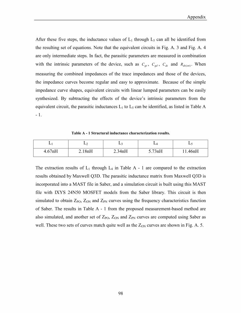
Appendix
98
After these five steps, the inductance values of L1 through L5 can all be identified from
the resulting set of equations. Note that the equivalent circuits in Fig. A. 3 and Fig. A. 4
are only intermediate steps. In fact, the parasitic parameters are measured in combination
with the intrinsic parameters of the device, such as gsC , gdC , dsC and )(ondsR . When
measuring the combined impedances of the trace impedances and those of the devices,
the impedance curves become regular and easy to approximate. Because of the simple
impedance curve shapes, equivalent circuits with linear lumped parameters can be easily
synthesized. By subtracting the effects of the device’s intrinsic parameters from the
equivalent circuit, the parasitic inductances L1 to L5 can be identified, as listed in Table A
- 1.
Table A - 1 Structural inductance characterization results.
L1 L2 L3 L4 L5
4.67nH 2.18nH 2.34nH 5.73nH 11.46nH
The extraction results of L1 through L4 in Table A - 1 are compared to the extraction
results obtained by Maxwell Q3D. The parasitic inductance matrix from Maxwell Q3D is
incorporated into a MAST file in Saber, and a simulation circuit is built using this MAST
file with IXYS 24N50 MOSFET models from the Saber library. This circuit is then
simulated to obtain ZPO, ZON and ZPN curves using the frequency characteristics function
of Saber. The results in Table A - 1 from the proposed measurement-based method are
also simulated, and another set of ZPO, ZON and ZPN curves are computed using Saber as
well. These two sets of curves match quite well as the ZON curves are shown in Fig. A. 5.
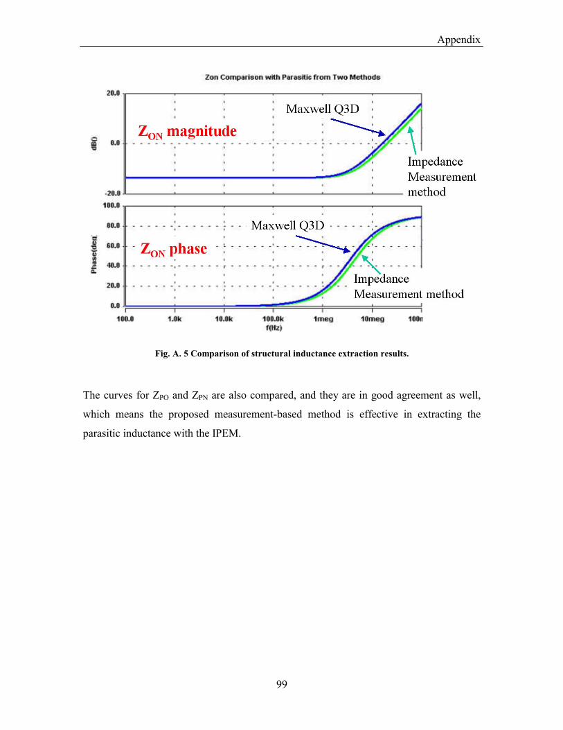
Appendix
99
Fig. A. 5 Comparison of structural inductance extraction results.
The curves for ZPO and ZPN are also compared, and they are in good agreement as well,
which means the proposed measurement-based method is effective in extracting the
parasitic inductance with the IPEM.

Appendix
100
2. Structural Capacitance Characterization
Since copper layers are plated on both the top and bottom surfaces of the ceramic layer in
the final IPEM module, structural capacitances exist in the active IPEM. These structural
capacitances provide propagation paths for the CM noise and are therefore important for
EMI analysis. Fig. A. 6 shows the DBC pattern and the existence of structural
capacitance.
Fig. A. 6 DBC pattern and the structural capacitance (device not incorporated).
The structural capacitances shown in Fig. A. 6 are in the order of tens of pF , which
means the impedance magnitude is extremely large in low frequencies. However, for
state-of-the-art impedance analyzers, such as the Agilent 4294A, capacitances of that
order still fall within the measurement range. Fig. A. 7 shows the measured impedance
between trace P and the back plane. As shown in Fig. A. 7, the impedance curve can be
approximated very well by a capacitor of 14.17pF. Impedance curves measured between
trace N and the back plane, or between trace O and the back plane, will have similar
shapes but different magnitudes. Please note that these results are obtained without
devices attached to the module.

Appendix
101
Fig. A. 7 Measured impedance between trace P and the back plane (without devices)
The equation dAC rεε0= is used to obtain estimated values of the structural capacitances.
The comparison between the estimated values and the measurement result is shown in
Table A - 2.
Table A - 2 Structural capacitance measurement and calculation.
(pF) CP CN CO
Equation 12.0 12.0 21.2
Measurement 14.2 13.5 22.4
According to Table A - 2, there should not be any problem in measuring the CM
capacitance. However, once the devices are soldered and wire-bonded onto the DBC
board, the measurement will be affected by the intrinsic capacitances of the devices. As
can be seen from Fig. A. 8, the intrinsic capacitances of the devices will also affect the
measurement results between the top layer traces and the back plane copper. Since the
intrinsic capacitances of the devices are much larger than the structural capacitances, they
provide low impedance paths between the structural capacitances CP, CO and CN.
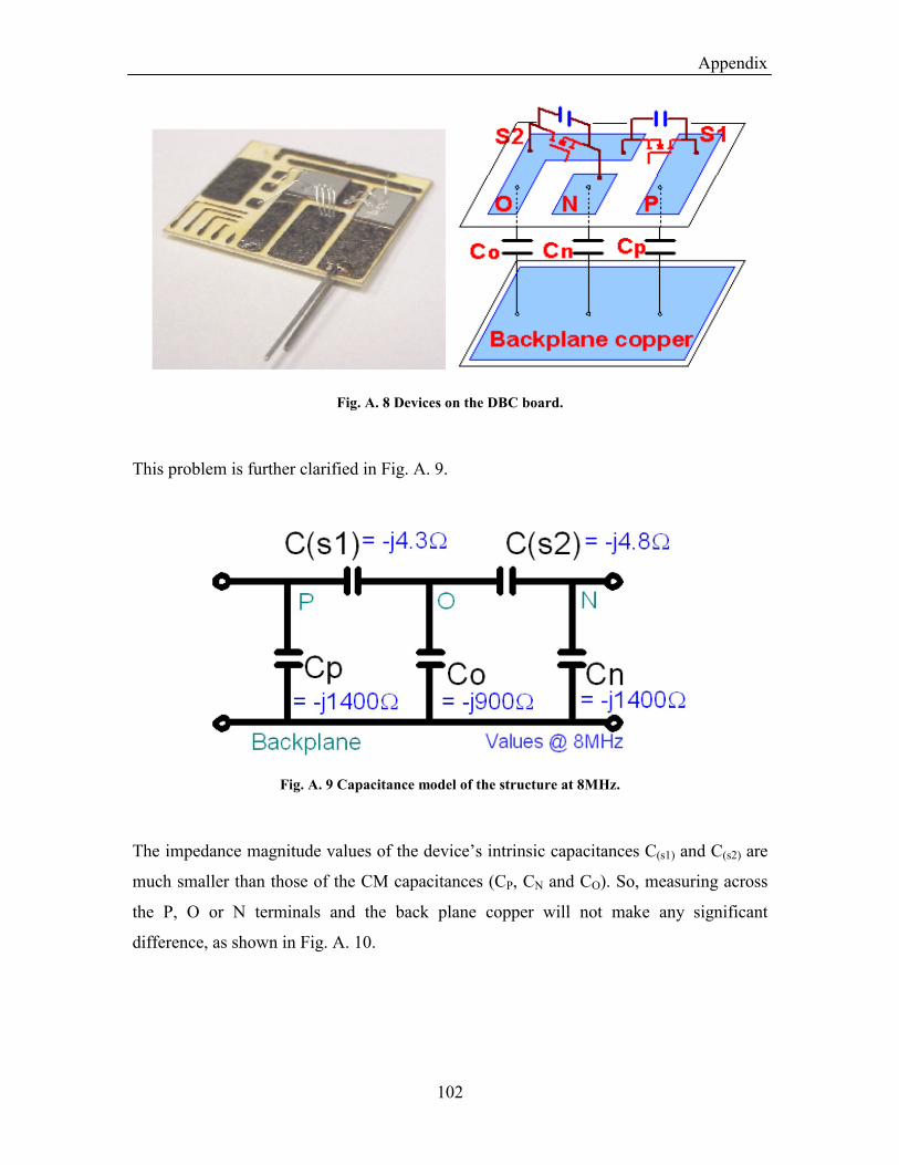
Appendix
102
Fig. A. 8 Devices on the DBC board.
This problem is further clarified in Fig. A. 9.
Fig. A. 9 Capacitance model of the structure at 8MHz.
The impedance magnitude values of the device’s intrinsic capacitances C(s1) and C(s2) are
much smaller than those of the CM capacitances (CP, CN and CO). So, measuring across
the P, O or N terminals and the back plane copper will not make any significant
difference, as shown in Fig. A. 10.

Appendix
103
Fig. A. 10 Measurement results comparison between different terminals and the back plane (with
devices).
Also, there will not be any significant difference between devices that are on or off, as
shown in Fig. A. 11. The reason is that the device in either state will be a low impedance
path between structural capacitances. The measurement results will always represent the
total value of those three CM capacitances.
Fig. A. 11 Measurement results comparison between trace P and the back plane for different states of
the devices.
Since these three structural capacitances make different contributions to CM noise (CO
will have dominant effect while CP and CN will have much less contribution), it is best to
identify their individual values. The challenge here is to identify their individual values
even after the devices have been packaged inside, which is also the common situation for
commercial module characterization. To solve this problem, it is desirable to make C(s1)

Appendix
104
and C(s2) open circuits, which will of course enable one to measure the individual
capacitances, as shown in Fig. A. 7. However, without destroying the structure it is
almost impossible to make the devices to open circuit state.
It is known that parallel resonance can produce high impedance that will ideally be open
circuit at its resonant frequency. Since the off-state devices show a capacitive
characteristic in the model shown in Fig. A. 9, it may be possible to make a parallel
resonance by paralleling an external inductor to the device. This alternative solution
enables one to produce high impedance without destroying the devices. Based on this
concept, several experiments are carried out to obtain measurement data that are used to
determine the individual values of CP, CO and CN. The extraction of the three CM
capacitances is performed through the following four steps.
Step 1: Measure the sum of the three capacitances, CTOTAL
Step 2: Extraction of CP
Step 3: Extraction of CN
Step 4: Since CTOTAL= CP+CN +CO, the value of CO can also be extracted
Details of the whole extraction process for this specific Active IPEM are described as
follows.
Step 1: Measure the sum of the three capacitors, CTOTAL
The measurement curve for Step 1 is shown in Fig. A. 12. Note that the two curves in the
magnitude plot are almost overlapped. The measured magnitude and phase curve can be
approximated by a 48.7pF capacitor. Although this result is measured between the P
terminal and the back plane, an almost identical curve can be obtained by measuring
between the N terminal and the back plane or between the O terminal and the back plane.
This capacitance is denoted as CTOTAL.

Appendix
105
Fig. A. 12 Measurement results and the approximation of CTOTAL
Step 2: Extraction of CP
Based on the parallel resonance concept mentioned before, an external inductor,
L1=120nH, will be added in parallel with top switch S1, as shown in Fig. A. 13.
To show the effect of parallel external inductance L1, comparisons will be made (referred
to Fig. A. 13) between the impedance across the P and O terminals (Z(po)) with and
without L1, as well as for Z(pb) with and without L1.
Fig. A. 13 External inductor L1 in parallel with S1 to produce resonance.

Appendix
106
The comparison of the Z(po) is shown in Fig. A. 14. The left-hand side is the impedance
without L1, while the result of the case with L1 is shown on the right side. As can be seen
from these two pictures, the magnitude of the Z(po) is enlarged to more than 90Ω at the
resonant frequency, which is 20 times of the original value. Although this 90Ω value is
still smaller than the individual impedance magnitudes of CP, CO and CN at that
frequency, this magnitude change still helps to solve the problem.
Fig. A. 14 Comparison of the impedances across the P and O terminals, without L1 (left) and with L1
(right).
Increasing the magnitude of the impedance between the P and O terminals will cause a
significant change in the Z(pb) curve (the impedance between the P terminal and the back
plane). As can be seen from Fig. A. 15, the phase changes from –90 degrees to –83
degrees.
Fig. A. 15 Comparison of Z(pb) without L1 (left) and with L1 (right).

Appendix
107
A Matlab program is used to identify the value of CP based on the impedance information
at the –83 degree frequency point, which is 7.46MHz. The value of Z(pb), measurement is
known from Fig. A. 15. CON is defined as the equivalent capacitance of CO, CN and C(s2).
Next, the values of CP and CON will be swept with a certain increment, 0.1pF in this case.
This means that each value of CP = 0pF, 0.1pF and 0.2pF up to 48.7pF and CON = 0pF,
0.1pF and 0.2pF up to 48.7pF will be tried one by one. For each value of CP and CON, one
can calculate the Z(pb), calculation since the value of Z(po) at that frequency point is known
from Fig. A. 14. The definition ncalculatiopbtmeasuremenpb ZZ ),(),( −=∆ is used. Among all the
combinations of CP and CON, there must be one combination that can produce the
imummin∆ . The CP value in this combination is considered to be the extraction result. With
the combination of CP=15.9pF and CON=36.2pF, Z(pb), calculation is closest to Z(pb), measurement.
Step 3: Extraction of CN
Using a method similar to that in Step 2, the value of CN can be extracted. This time an
external inductor L2=120nH will be put in parallel with the intrinsic capacitances of
bottom switch S2, as shown in Fig. A. 16.
Fig. A. 16 External inductor L2 in parallel with S2 to produce resonance

Appendix
108
Using this configuration, the value of Z(bn), measurement can be measured. By sweeping the
value of CN and CPO (the equivalent capacitance of CP, CO and C(s1)), one can search for
the imummin∆ , where ∆ in this step is defined as ncalculatiobntmeasuremenbn ZZ ),(),( −=∆ . The CN
value that produces imummin∆ is considered to be the extraction result.
With CN=11.5pF and CPO=36.7pF, Z(bn), calculation is closest to Z(bn), measurement.
To test whether the mathematical method for the CP and CN extraction is sensitive to the
inductor value, measurement data are also collected for another two different inductors’
values, 10uH and 1mH. Paralleling a 10uH inductor with bottom switch S2 will produce a
parallel resonance peak at around 800KHz, as can be seen on the right side of Fig. A. 17.
Using the Z(on) and Z(bn) data at this resonant peak frequency, the CN and the CPO values
are identified as 12.3pF and 37.9pF, respectively.
Fig. A. 17 Impedances across the O and N terminals with L2=10uH.
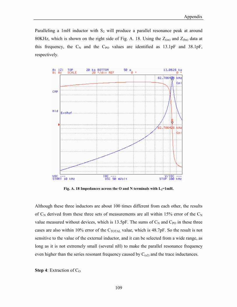
Appendix
109
Paralleling a 1mH inductor with S2 will produce a parallel resonance peak at around
80KHz, which is shown on the right side of Fig. A. 18. Using the Z(on) and Z(bn) data at
this frequency, the CN and the CPO values are identified as 13.1pF and 38.1pF,
respectively.
Fig. A. 18 Impedances across the O and N terminals with L2=1mH.
Although these three inductors are about 100 times different from each other, the results
of CN derived from these three sets of measurements are all within 15% error of the CN
value measured without devices, which is 13.5pF. The sums of CN and CPO in these three
cases are also within 10% error of the CTOTAL value, which is 48.7pF. So the result is not
sensitive to the value of the external inductor, and it can be selected from a wide range, as
long as it is not extremely small (several nH) to make the parallel resonance frequency
even higher than the series resonant frequency caused by C(s2) and the trace inductances.
Step 4: Extraction of CO

Appendix
110
Since CTOTAL= CP+CN +CO, the value of CO can be identified according to the CTOTAL, CP,
and CN values determined in the previous three steps.
Upon completion of these four steps, the individual values of CP, CO and CN have been
identified for the case that the MOSFET devices have been packaged into the IPEM. The
results are shown in Table A - 3.
Table A - 3 Structural capacitance value determination.
(pF) CP CN CO
Proposed method 15.9 11.5 21.3
Measurement without device 14.2 13.5 22.4
Based on the comparison results given in Table A - 3, the proposed method for the
structural capacitances extraction can be used to determine the values of structural
capacitance without intrusion into the structure.

Vita
111
Vita
Liyu Yang
The author was born in Rong County, Guangxi, China in 1976. He received the B. S.
degree from Zhejiang University in 1999. From February 2000 to July 2001, he was
employed as an engineer in the research and development department of the Huawei
Electric Corporation, China.
Since August 2001, he has been working towards the Master of Science degree at the
Bradley Department of Electrical and Computer Engineering, Virginia Polytechnic
Institute and State University. Working as a research assistant at the Center for Power
Electronics Systems, his research interest includes EMI modeling and prediction,
parasitic parameter extraction using software and measurement-based methods, and high
frequency DC/DC converter design.