Model SR844 RF Lock-In Amplifier - Stanford Research … · 2018-05-08 · ii . SR844 RF Lock-In...
246
User’s Manual Model SR844 RF Lock-In Amplifier 1290-D Reamwood Avenue Sunnyvale, California 94089 Phone: (408) 744-9040 • Fax: (408) 744-9049 email: [email protected] • www.thinkSRS.com Copyright © 1997, 2007, 2013 by SRS, Inc. All Rights Reserved. Revision 2.9 (07/2016)
Transcript of Model SR844 RF Lock-In Amplifier - Stanford Research … · 2018-05-08 · ii . SR844 RF Lock-In...

User’s Manual
Model SR844 RF Lock-In Amplifier
1290-D Reamwood Avenue Sunnyvale, California 94089
Phone: (408) 744-9040 • Fax: (408) 744-9049 email: [email protected] • www.thinkSRS.com
Copyright © 1997, 2007, 2013 by SRS, Inc.
All Rights Reserved.
Revision 2.9 (07/2016)

SR844 RF Lock-In Amplifier
Certification Stanford Research Systems certifies that this product met its published specifications at the time of shipment. Stanford Research Systems further certifies that its calibration measurements are traceable to the United States National Institute of Standards and Technology (NIST).
Warranty This Stanford Research Systems product is warranted against defects in materials and workmanship for a period of one (1) year from the date of shipment.
Service For warranty service or repair, this product must be returned to a Stanford Research Systems authorized service facility. Contact Stanford Research Systems or an authorized representative before returning this product for repair. Information in this document is subject to change without notice. Copyright © Stanford Research Systems, Inc., 1997, 2007, 2013, 2016. All rights reserved. Stanford Research Systems, Inc. 1290-D Reamwood Avenue Sunnyvale, California 94089 Printed in U.S.A.

i
SR844 RF Lock-In Amplifier
Safety and Preparation For Use WARNING! Dangerous voltages, capable of causing injury or death, are present in this
instrument. Use extreme caution whenever the instrument cover is removed. Do not remove the cover while the unit is plugged into a live outlet.
Caution This instrument may be damaged if operated with the LINE VOLTAGE SELECTOR set
for the wrong AC line voltage or if the wrong fuse is installed. Line Voltage The SR844 operates from a 100V, 120V, 220V, or 240V nominal AC power source Selection having a line frequency of 50 or 60 Hz. Before connecting the power cord to a power
source, verify that the LINE VOLTAGE SELECTOR card, located in the rear panel fuse holder, is set so that the correct AC input voltage value is visible.
Conversion to other AC input voltages requires a change in the fuse holder voltage card position and fuse value. Disconnect the power cord, open the fuse holder cover door and pull the fuse-pull lever to remove the fuse. Remove the small printed circuit board and select the operating voltage by orienting the printed circuit board so that the desired voltage is visible when the circuit board is pushed firmly into its slot. Push the fuse-pull lever back into its normal position and insert the correct fuse into the fuse holder.
Line Fuse Verify that the correct line fuse is installed before connecting the line cord. For 100V/120V, use a 1 Amp fuse and for 220V/240V, use a 1/2 Amp fuse.
Line Cord The SR844 has a detachable, three-wire power cord for connection to the power source
and to a protective ground. The exposed metal parts of the instrument are connected to the outlet ground to protect against electrical shock. Always use an outlet which has a properly connected protective ground.
Service Do not attempt to service or adjust this instrument unless another person, capable of
providing first aid or resuscitation, is present. Do not install substitute parts or perform any unauthorized modifications to this
instrument. Contact the factory for instructions on how to return the instrument for authorized service and adjustment.
Fan The fans in the SR844 are required to maintain proper operation. Do not block the vents in the chassis or the unit may not operate properly.
Warning! Regarding Use With Photomultipliers and Other Detectors The front end amplifier of this instrument is easily damaged if a photomultiplier is used
improperly with the amplifier. When left completely unterminated, a cable connected to a PMT can charge to several hundred volts in a relatively short time. If this cable is connected to the inputs of the SR844 the stored charge may damage the front-end op ampls. To avoid this problem, always connect the PMT output to the SR844 input before turning the PMT on.

ii
SR844 RF Lock-In Amplifier
Symbols that may be found on SRS products
Symbol Description
Alternating current
Caution - risk of electric shock
Frame or chassis terminal
Caution - refer to accompanying documents
Earth (ground) terminal
Battery
Fuse
On (supply)
Off (supply)

iii
SR844 RF Lock-In Amplifier
Contents
General Information Safety and Preparation For Use i Contents iii Specifications v
Chapter 1 Getting Started Quick Start 1-3 The Basic Lock-In 1-5 X, Y, R, θ and dBm 1-9 Outputs, Offsets and Expands 1-12 Storing and Recalling Setups 1-18 Aux Outputs and Inputs 1-19
Chapter 2 SR844 Basics What is a Lock-In Amplifier? 2-3 The Functional SR844 2-8 RF Signal Input Path 2-9 Reference Channel 2-10 I.F. Section 2-11 Inside the DSP 2-12 Analog Outputs and Scaling 2-15 What is Dynamic Reserve ? 2-17 Sources of Error 2-19 Using the SR844 as a Double Lock-In 2-22 Noise Measurements 2-23 Intrinsic (Random) Noise Sources 2-24 External Noise Sources 2-25
Chapter 3 Operation Overview 3-3 Signal Input 3-8 Time Constants 3-11 Sensitivity 3-13 CH1 Display and Output 3-15 CH2 Display and Output 3-20 Reference Section 3-26 Save and Recall 3-30 Interface 3-31 Scan and Rel 3-33 Auto Functions 3-40 Shift Functions 3-41

iv Contents
SR844 RF Lock-In Amplifier
Chapter 4 Programming Index of Commands 4-2 Introduction 4-7 Command Syntax 4-10 Status Register Definitions 4-31 Example Program 4-34
Chapter 5 Testing Getting Ready 5-3 Self Test 5-5 Amplitude Response 5-7 Phase Response 5-9 Frequency Accuracy 5-11 Ref Out Amplitude 5-13 DC Outputs and Inputs 5-15 Input Noise 5-17 SR844 Performance Test Record 5-19
Chapter 6 Circuitry Service 6-3 Circuit Board Locations 6-4 Circuit Descriptions 6-6 Parts Lists 6-25 Schematic Diagrams 6-80

v
SR844 RF Lock-In Amplifier
Specifications Specifications apply after 30 minutes of warm-up. All specifications are with output filtering enabled (6, 12, 18 or 24 dB/oct) and 2F detection OFF, unless stated otherwise.
Signal Input Voltage Input single-ended BNC. Input Impedance 50 Ω or 1 MΩ || 30 pF. Damage Threshold ±5 V (DC+AC) Bandwidth 25 kHz to 200 MHz. Full Scale Sensitivity 100 nV to 1V rms in a 1-3-10 sequence. Gain Accuracy < 50 MHz ±0.25 dB < 200 MHz ±0.50 dB Gain Stability 0.2%/°C Coherent Pickup Low Noise Wide Reserve, Sensitivity < 30 mV. f < 10 MHz < 100 nV (typical) f < 50 MHz < 2.5 µV (typical) f < 200 MHz < 25 µV (typical) Input Noise: 50 Ω Input 100 kHz < f < 100 MHz 2 nV/√Hz (typical), < 4 nV/√Hz (max). 25 kHz < f < 200 MHz < 5 nV/√Hz (typical), < 8 nV/√Hz (max). Input Noise: 1 MΩ Input 25 kHz < f < 200 MHz 5 nV/√Hz (typical), < 8 nV/√Hz (max). Dynamic Reserve > 60 dB (expand off)
Reference External Reference Input 25 kHz to 200 MHz. Impedance 50 Ω or 10 kΩ || 40 pF. Level 0.7 Vpp digital or 0 dBm sinusoidal signal. Pulse Width > 2 ns at any frequency. Threshold Setting Automatic, set to midpoint of waveform extrema. Acquisition Time < 10 s (auto-ranging, any frequency).
< 1 s (within same octave). Internal Reference Oscillator 25 kHz to 200 MHz. Frequency Resolution 3 digits. Frequency Accuracy ±0.1 in the 3rd digit. Phase Noise -90 dBc/Hz at f=100 MHz, ∆f=100 Hz. Reference Outputs Phase locked to either Internal or External reference. Front Panel Ref Out 25 kHz to 200 MHz square wave, 1.0 Vpp nominal into 50 Ω. Rear Panel TTL Out 25 kHz to 1.5 MHz, 0 to +5 V nominal, ≥ 3 V into 50 Ω. Harmonic Detect Detect at 50 kHz ≤ 2×Reference ≤ 200 MHz. Phase Resolution 0.02° Absolute Phase Error < 50 MHz < 2.5° < 100 MHz < 5.0° < 200 MHz < 10.0°

vi Specifications
SR844 RF Lock-In Amplifier
Reference Relative Phase Error, Orthogonality
< 2.5°
Phase Noise 0.005° rms at 100 MHz, 100 ms time constant. Phase Drift < 10 MHz < 0.1°/°C < 100 MHz < 0.25°/°C < 200 MHz < 0.5°/°C
Demodulator Zero Stability Digital displays have no zero drift.
Analog outputs have < 5ppm/°C drift for all dynamic reserve settings. Filtering Time Constants 100 µs to 30 ks with 6, 12, 18 or 24 dB/octave roll-off. None 10 to 20 µs update rate (X and Y outputs), 60 µs (R and θ outputs). Harmonic Rejection Odd Harmonics -10 dBc @ 3×Ref, -14 dBc @ 5×Ref, etc. Other Harmonics and
Sub-harmonics < -40 dBc
Spurious Responses -10 dBc @ Ref ± 2×IF -23 dBc @ Ref ± 4×IF < -30 dBc otherwise.
Displays Channel 1 Channel 2 Reference
Type 4½ digit LED 4½ digit LED 4½ digit LED Displayed X Y Reference Frequency Quantities R [Volts] θ [degrees] Reference Phase R [dBm] Y-noise [Volts] Aux Output Voltages X-noise Y-noise [dBm] Offsets in % of Full Scale AUX IN 1 AUX IN 2 IF Frequency Elapsed Settling Time Ratio The signal may be ratioed with respect to AUX IN 1 or
2. The ratio is applied to both X and Y before computation of R, R[dBm], X-noise, Y-noise [V, dBm] and so affects all of these quantities. The ratio input is normalized to 1 V and has a dynamic range > 100.
Expand The CH1 and CH2 displays and outputs may be expanded by ×10 or ×100.

Specifications vii
SR844 RF Lock-In Amplifier
CH1 and CH2 Outputs Connectors Front Panel BNC. Voltage Range ±10V full scale proportional to X, Y or CH1, CH2 displayed quantity.
±11V full scale for phase Update Rate X, Y 48 to 96 kHz R, θ, Aux Inputs 12 to 24 kHz X Noise, Y Noise 512 Hz
Aux Inputs and Outputs Connectors Rear Panel BNC. Inputs 2 Type
Range Differential with 1 MΩ input impedance on both signal and shield. ±10V
Resolution 1/3 mV Bandwidth 3 kHz Outputs 2 Range ±10V Resolution 1 mV
Environmental Conditions Operating Temperature: +10°C to +40°C
(Specifications apply over +18°C to +28°C) Relative Humidity: <90% Non-condensing
Non-Operating Temperature: –25°C to +65°C Relative Humidity: <95% Non-condensing
General Furnished Accessories Power Cord
Operating Manual Interfaces IEEE-488.2 and RS232 interfaces standard. All instrument functions
can be controlled and read through either interface. Power 70 Watts, 100/120/220/240 VAC, 50/60 Hz. Dimensions 17" W x 5.25" H x 19.5" D Weight 23 lb. Warranty One year parts and labor on materials and workmanship.

viii
SR844 RF Lock-In Amplifier

1-1
SR844 RF Lock-In Amplifier
Chapter 1
Getting Started
The tutorials in this chapter are designed to acquaint the first time user with the SR844 RF Lock-InAmplifier. The functions and features of the SR844 are grouped together into several short tutorials. Youmay choose to do the tutorials selectively depending on your level of experience and your measurementneeds. Do not be concerned that your measurements do not agree exactly with the printed values in themanual; the focus of these exercises is to learn how to use the instrument.
For all of the tutorials it is expected that you have installed the instrument with the line voltage settingappropriate to the AC power available. If you have not done so, please see the section Line VoltageSelection under Safety and Preparation for Use (page i) before proceeding further.
The experimental procedures are detailed in two columns. The left column lists the actual steps to beperformed. The right column is an explanation of each step. The front panel Keys, Knob andREADOUTS are denoted in special fonts. Indicators are shown in Bold and connectors in CAPITALS.
In This Chapter Quick Start 1-3
The Basic Lock-In 1-5
X, Y, R, θθθθ and dBm 1-9
Outputs, Offsets and Expands 1-12
Storing and Recalling Setups 1-18
Aux Outputs and Inputs 1-19

1-2 Getting Started
SR844 RF Lock-In Amplifier

Quick Start 1-3
SR844 RF Lock-In Amplifier
Quick Start This section will lead you through the most basic setup and use of the SR844 RF lock-in amplifier. Youmust have selected the line voltage (page i) and connected AC power in order to proceed further.
For this section you will need one BNC cable.
1 Disconnect all cables from the SR844. Checkthat the power cord is connected.
2 Turn the power on while holding down theSetup key.
If the Setup key is pressed during power-on, theinstrument performs power-on tests and returns toits factory preset settings.
3 Wait until the power-on tests are completed. The instrument first displays SR844 followed bythe unit’s serial number (CH1 and CH2 displays)and the firmware revision number (Referencedisplay).
Several tests are performed after this. The messageDATA TEST PASS follows a read/write test tothe processor RAM. BATT TEST PASS refers toa test of the battery-backed-up memory. PROGTEST PASS follows a test of the instrumentprogram ROM. DSP TEST PASS refers to theDigital Signal Processor (DSP). RCAL STD SETis shorthand for Recall Standard Setup (factorydefaults). Normally, the Setup button is not pressedduring power-up and the last message will insteadbe RCAL USER SET , which means that theprevious User’s setup has been recalled.
4 If any of the tests FAIL, try power-on oncemore with the Setup button held down. If thetest FAILs again, note the ROM version andSerial Number and contact either the factoryor your local representative.
5 Connect REF OUT on the front panel to theSIGNAL IN with the BNC cable.
The SR844 defaults to the internal oscillator set at1.00 MHz. The reference mode is indicated by theINTERNAL LED. In this mode the SR844generates a reference signal at the selectedfrequency and detects input signals in phase and inquadrature with this reference. A 1.0 Vpp squarewave reference signal is available at REF OUT.

1-4 Quick Start
SR844 RF Lock-In Amplifier
At 1 MHz, a quarter wavelength is roughly 50 meters of BNC cable. Your BNC cable is probably a lot shorter than this, so the signal input is close to being in phase with the reference.
6 Check the readings on the front panel displays.
Press CH1 Display to select R [dBm]. The R[dBm] display on CH1 should read +5.6 to +9.6 dBm.

The Basic Lock-In 1-5
SR844 RF Lock-In Amplifier
The Basic Lock-In This measurement is designed to use the internal oscillator to explore some of the basic lock-inoperations. You should already be familiar with the fundamentals of lock-in detection. See Chapter 2 for adiscussion of the basics of lock-in measurements.
Specifically, you will measure the amplitude of the reference oscillator at various frequencies,sensitivities, time constants and phases. You will need a BNC cable for this section.
1 Disconnect all cables from the SR844.
If the power is off, turn it on. Wait for self-tests to complete.
Turn on the unit.
2 Press Shift then Recall (PRESET) to restorefactory presets.
We will start with the unit in its factory presetconfiguration.
The factory preset configuration is InternalReference mode (shown by the INTERNAL LED)at 1.00 MHz, shown on the Reference display.
The time constant is 100 ms (shown by the timeconstant indicators 1, ××××100 and ms above the TimeConstant Up/Down keys) and the sensitivity is 1 Vrms (the indicators are below the SensitivityUp/Down keys).
3 Connect REF OUT on the front panel to theSIGNAL IN with the BNC cable.
The SR844 reference output (1.0 Vpp nominalsquare wave into 50 Ω) is within the unit’smeasurement range (1 Vrms) so we can connect itdirectly to the input. The SR844 input impedance isset to 50 Ω (shown by the 50 ΩΩΩΩ indicator) which isappropriate for the REF OUT.
The BNC cable has a small phase shift at 1 MHz(the free-space wavelength is 300 m), so the inputsignal should be mostly X (in-phase) with a small Y(quadrature) component.
The CH1 Display is set to X and should showsomething close to 0.54 V. The CH2 display is setto Y and should show less than ±0.05 V.

1-6 The Basic Lock-In
SR844 RF Lock-In Amplifier
Remember, the signal is a 0.5 Vpk (1.0 Vpp) squarewave. A square wave is composed of signals at allodd harmonics. The SR844 is a square wavedetecting lock-in and detects all of the oddharmonics of the fundamental. The amplitude of thefundamental (at 1.00 MHz) is 4/π x Vpk. Thecontribution from all odd harmonics is
1 + (1/3)2 + (1/5)2 + (1/7)2 + ... ≈ 1.19
The detected amplitude is 4/π x 0.5 Vpk x 1.19 or0.759 Vpk. The SR844 reads the signal in units ofVrms (0.707 x Vpk) or 0.537 Vrms.
The CH1 display may not read exactly 0.54 V for anumber of reasons:
• The REF OUT amplitude is only a nominalspecification.
• The basic accuracy of the unit is ±0.25 dB(3%).
• Since the phase may not be exactly 0°, X=Rcosθis slightly less than R (amplitude).
4 Press Shift then Phase to performAutoPhase.
This adjusts the reference phase inside theinstrument. (The phase at which the signal isdetected changes, but Ref Out remains unchanged.)This should set the value of Y (on the CH2 display)to zero.
5 Press Phase. Display the reference phase. It should be close tozero.
6 Press the +90° key. This adds 90° to the reference phase. The value ofX should drop to near zero, while Y changes toabout –0.54 V (negative of the previous X reading).
7 Use the knob to adjust the reference phaseuntil Y is zero and X is equal to the positiveamplitude.
While the reference phase is being displayed, theknob can be used to change it. The adjustmentdescribed should result in the phase returning tonearly zero again.
In general, the knob is used to adjust the quantitydisplayed in the Reference display (if it can bechanged). The keys below the display are used toselect the desired quantity.

The Basic Lock-In 1-7
SR844 RF Lock-In Amplifier
8 Press Freq. Now the display shows the reference frequency, still1.00 MHz.
9 Rotate the knob left to get to 999 kHz and998 kHz.
The internal frequency may be adjusted with 3-digitresolution.
Rotate the knob right to get to 1.01 MHz and1.02 MHz.
The actual frequency is within 1 count in the 4thdigit of the displayed frequency. For example, whenset to 4.56 MHz, the actual frequency is within0.001 MHz of 4.56 MHz.
10 Use the knob to adjust the frequency to96 kHz.
The X reading should vary less than 10%.
11 Press Sensitivity Down. The sensitivity changes to 300 mV (indicated belowthe Sensitivity Down key). The OVLD indicatorsin the CH1 and CH2 displays indicate that thereadings may be invalid due to an overloadcondition. OVLD indicators in the Input, TimeConstant and Sensitivity areas are used to pinpointthe source of the overload.
12 Press Shift then Sensitivity Up to performAutoSensitivity.
This adjusts the sensitivity so that the measuredmagnitude, R, is a sizable percentage of full scale.The instrument should end up on the 1 V scale andthe displays showing their previous values.
13 Disconnect the cable at the SIGNAL INconnector.
Watch the CH1 display bargraph drop down to zero.The time constant is 100 ms, the bargraph fallsquickly but not instantaneously.
14 Reconnect the cable to SIGNAL IN. Watch the CH1 bargraph come back up.
15 Press Time Constant Down six times untilthe time constant is 100 µs.
The Time Constant is adjusted using the left handpair of keys in the Time Constant area. Theindicated time constant should be 1, x100, µµµµs . TheCH1 and CH2 values remain nearly unchanged butmay be noisy in the last digit.
16 Disconnect the cable at the SIGNAL INconnector, then reconnect it.
The bargraph falls and rises nearly instantaneously.
17 Press Time Constant Up until the timeconstant is 3 s.
The indicated time constant should be 3, x1,s. TheCH1 and CH2 displays remain nearly unchanged.
18 Disconnect the cable at the SIGNAL INconnector. Wait until the CH1 reading dropsto zero.
The bargraph falls slowly.

1-8 The Basic Lock-In
SR844 RF Lock-In Amplifier
19 Reconnect the cable to SIGNAL IN. The bargraph rises slowly. In fact, with a filter slopeof 12 dB/oct, it takes about 5 time constants to getto within 1% of the final reading. In this case, thistakes more than 15 s.
20 Press Slope/Oct DOWN until 24 dB isselected.
The filter slope is adjusted using the right hand pairof keys in the Time Constant area. The filter rolloffcan be 6, 12, 18 or 24 dB/oct.
With 24 dB/oct rolloff, it takes about 12 timeconstants to get within 1% of the final reading.
Remember, both the time constant and filter slopeaffect the output settling time.
21 Press Slope/Oct UP until NO FILTER isselected.
No filtering is also available. In this case, thedemodulator outputs are amplified but not filtered.The high output bandwidth in this case requires thatthe outputs be taken from the CH1 or CH2OUTPUT from the front panel and not from thedisplays.
22 Press Slope/Oct DOWN until 12 dB isselected.
12 dB/oct works well in most situations.

X, Y, R, θθθθ and dBm 1-9
SR844 RF Lock-In Amplifier
X, Y, R, θθθθ and dBm This measurement is designed to use the internal oscillator and an external signal source to explore someof the signal types. You will need a synthesized signal generator cable of providing 200 mVrms (0 dBm)sine waves at 100 kHz into a 50 Ω load (the DS335 from Stanford Research Systems will suffice), andBNC cables.
Specifically you will display the lock-in outputs when measuring a signal that has a frequency close to,but not equal to, the internal reference frequency.
Note: The last few items in this section require that the signal generator have a Sync output; if you areusing a signal generator that has a single output only, you can split the output using a BNC Tee (or apower splitter or a directional coupler).
1 Disconnect all cables from the SR844.
If the power is off, turn it on. Wait for self-tests to complete.
Turn on the unit.
2 Press Shift then Recall (PRESET) to restorefactory presets.
The factory preset configuration is:1 Vrms sensitivity.100 ms, 12 dB/oct time constant.Internal Reference at 1.00 MHz.Signal Input 50 Ω.
3 Use the knob to adjust the SR844 referencefrequency to 100 kHz.
We are using a low reference frequency so that theintrinsic frequency difference between the SR844and the signal generator has a smaller absolutevalue.
4 Press Sensitivity Down.
Press Time Constant Down twice until thetime constant is 10 ms.
The SR844 sensitivity should now be 300 mVrms.
We need a shorter time constant to measure theoutput signal.
5 Turn on the external signal generator and setthe frequency to 100 kHz exactly, and theamplitude to 200 mVrms, 0 dBm, or600 mVpp into 50 Ω. The exact value doesn’treally matter. Low-frequency signal generatorsmay have waveform selection (select sinewave) and DC offset (set it to zero). If thesignal generator offers modulation, make sureit’s off.
While not phase-locked, the signal generator andSR844 should be at very nearly the same frequency;the slight frequency difference will be manifested asa changing relative phase.

1-10 X, Y, R, θθθθ and dBm
SR844 RF Lock-In Amplifier
6 Connect the signal generator output to theSR844 SIGNAL IN connector with a BNCcable.
The CH1 and CH2 readings should both varybetween positive and negative values in a correlatedfashion that reflects the changing relative phasebetween the two instruments.
7 Adjust the signal generator frequency ifnecessary to better match the signal generatorfrequency to the SR844.
The extent of adjustment should be less than 10 Hz.
8 Adjust the signal generator frequency in stepsof 1 Hz (or less) until the CH1 and CH2readings oscillate with a period of a fewseconds.
The CH1 and CH2 display bargraphs should nowoscillate slowly.
9 Press CH1 Display once to select R [V]. R is the signal amplitude and is independent ofreference phase ( R=√(x2+y2) ). The reading of Rdoes not oscillate.
10 Press CH1 Display to select R [dBm]. The R[dBm] display on CH1 should read within afew dB of 0 dBm (0.224 Vrms) depending upon theamplitude setting of the signal generator.
11 Adjust the signal generator amplitude to halfthe original amplitude (100 mVrms, –6 dBm,or 300 mVpp).
The R[dBm] display should drop by 6 dBm.
12 Press CH1 Display several times until R [V]is selected once again.
The Display key cycles through the availablechoices.
13 Press CH2 Display to select θ. CH2 now shows the signal phase θ. The phase ischanging linearly with a rate equal to the frequencydifference between the signal generator and theSR844. The readout and bargraph ramp linearly andsmoothly from –180° to +180° (or vice-versa) onceeach period. When displaying θ, the bargraph on theCH2 display is scaled from -180° (extreme left) to+180° (extreme right).
14 Press the Source key (above REF OUT). Switch the SR844 to External Reference Mode.Since there is no external reference input connectedyet, the Reference Display should read about19 kHz (the internal oscillator pulls to its lowestfrequency) and the red OUT OF RANGE andUNLOCK indicators should be lit.

X, Y, R, θθθθ and dBm 1-11
SR844 RF Lock-In Amplifier
15 Connect the Sync output of the signalgenerator to the REF IN connector of theSR844 with a BNC cable.
The SR844 locks to the signal generator frequency,and the R and θ displays are both stable. Check thatthe UNLOCK error indicator (above the knob) isoff.
Note: If you are using a signal generator witha single output, split the output using a BNCTee, or a power splitter or 10 to 20 dBdirectional coupler. (If you use a directionalcoupler the straight-through output should goto REF IN and the coupled output should goto the SIGNAL IN.) You may need to adjustthe signal generator amplitude to provide theSR844 with enough signal to lock, and youmay need to adjust the SR844 sensitivity sothat the signal amplitude, R, is a sizablefraction of the full scale range.
If the REF IN signal is noisy or too small, theSR844 may not be able to lock. The referencesignal should be greater than 0.6 Vpp. If the signalgenerator Sync output cannot drive 50 Ω to a largeenough amplitude, try changing the Reference InputImpedance to 10 kΩΩΩΩ by pressing the Ref Z-In key.
16 Change the signal generator frequency to 1.00MHz.
The SR844 UNLOCK error indicator comes onbriefly, then goes off to indicate that the SR844 haslocked to the new frequency. The new frequencyshould be correctly displayed in the Referencedisplay.
The displayed value of R should not change(depending upon the amplitude flatness of the signalgenerator and the accuracy of the SR844). Thevalue of θ may change a few degrees dependingupon the signal generator Sync phase and cablelengths.

1-12 Outputs, Offsets and Expands
SR844 RF Lock-In Amplifier
Outputs, Offsets and Expands This measurement is designed to use the internal oscillator to explore some of the basic lock-in outputs.You will need BNC cables and a digital voltmeter (DVM).
Specifically, you will measure the amplitude of the reference oscillator and provide analog outputsproportional to the measurement. The effect of offsets and expands on the displayed values and the analogoutputs will be explored.
1 Disconnect all cables from the Lock-In.
If the power is off, turn it on. Wait for self-tests to complete.
Turn on the unit.
2 Press Shift then Recall (PRESET) to restorefactory presets.
The factory preset configuration is:1 Vrms sensitivity.100 ms, 12 dB/oct time constant.Internal Reference at 1.00 MHz.Signal Input 50 Ω.
3 Connect REF OUT on the front panel to theSIGNAL IN with the BNC cable.
The SR844 reference output (1.0 Vpp nominalsquare wave into 50 Ω) is within the unit’smeasurement range (1 Vrms) so we can connect itdirectly to the input. The SR844 input impedance isset to 50 Ω (shown by the 50 ΩΩΩΩ indicator) which isappropriate for the REF OUT.
The CH1 Display is set to X and should showsomething close to 0.54 V. The CH2 display is setto Y and should show less than ±0.05 V.
Remember, the signal is a 0.5 Vpk (1.0 Vpp) squarewave. A square wave is composed of signals at allodd harmonics. The SR844 is a square wavedetecting lock-in and detects all of the oddharmonics of the fundamental. The amplitude of thefundamental (at 1.00 MHz) is 4/π x Vpk. Thecontribution from all odd harmonics is
1 + (1/3)2 + (1/5)2 + (1/7)2 + ... ≈ 1.19
The detected amplitude is 4/π x 0.5 Vpk x 1.19 or0.759 Vpk. The SR844 reads the signal in units ofVrms (0.707 x Vpk) or 0.537 Vrms.

Outputs, Offsets and Expands 1-13
SR844 RF Lock-In Amplifier
The CH1 display may not read exactly 0.54 V for anumber of reasons:
• The Ref Out amplitude is only a nominalspecification.
• The basic accuracy of the unit is ±0.25 dB(3%).
• Since the phase may not be exactly 0°, X=Rcosθis slightly less than R (amplitude).
4 Connect the CH1 OUTPUT to the DVM. Setthe DVM to read DC Volts, on the 20 Vdcscale.
The CH1 output is preset to X as indicated by the XLED above the CH1 OUTPUT. The output voltageis given by the formula:
(X/Sensitivity – Xoffset) × Expand × 10V
In this case X ≅ 0.54 Vrms, Sensitivity = 1.0 Vrms,Xoffset = 0, Expand = 1 (no output expand), so weexpect the DC output voltage to be about 5.4 V.The DVM should read about this value (dependingupon the exact X reading).
5 Press CH1 Offset Auto (this key is two keysleft of the CH1 OUTPUT connector).
X, Y and R may all be offset and expandedindependently.
Since Channel 1 is displaying X, the Offset (On/Off,Auto and Modify) and Expand keys below theChannel 1 Display set the offset and expand for X.The display selection determines which quantity theOffset and Expand keys operate on.
Offset Auto automatically adjusts the offset of thedisplayed quantity to make the result zero. In thiscase, X is offset to zero. (Y is also offset to zero.See below for an explanation of X and Y offsets.)
The offset affects both the displayed value of X andthe CH1 analog output (X). Thus, after the autooffset function is performed, both the displayedvalue of X and the DVM should show readings veryclose to zero.
The XYOffs indicator in the Channel 1 Display hasturned on to indicate that the display quantity isaffected by XY offsets.
Offsets are useful for making relative measurementsor to cancel the contribution from an unwantedphase coherent signal. In analog lock-ins, offsets

1-14 Outputs, Offsets and Expands
SR844 RF Lock-In Amplifier
were generally used to remove DC output errorsfrom the lock-in itself. The SR844 demodulator isdigital and has no DC output errors, however, itdoes have some coherent pickup at highfrequencies, which can be canceled using offsets.
Important!Xoffset and Yoffset are applied to the X and Ydemodulator outputs directly. R and θ are computedfrom the offset values of X and Y. Offsetting X orY changes the measurement of R and θ.
In addition, changing the Reference Phase willmodify the values of Xoffset and Yoffset. Think of(Xoffset, Yoffset) as a signal vector relative to theReference (internal or external) which cancels anactual signal at the input. This cancellation ispreserved even when the detection phase (ReferencePhase) is changed. This is done by circularlyrotating the values of Xoffset and Yoffset by minusthe Reference Phase. This preserves the phaserelationship between (Xoffset, Yoffset) and thesignal input.
Since the vector (Xoffset, Yoffset) is used to cancela real signal at the input, Xoffset and Yoffset arealways turned on and off together. Turning either Xor Y offset on (or off) turns on (or off) both offsets.Auto offsetting either X or Y performs auto offseton both X and Y. These statements are true even ifonly one of the quantities X or Y is currently beingdisplayed.
6 Press Phase to display the Reference Phasein the Reference Display.
Since auto offset has set (Xoffset, Yoffset) to cancelthe signal input, changing the Reference Phase doesnot affect the X and Y readings.
Press the +90° key. X and Y remain zero even as the phase is changed.This allows phase coherent signals at the input to becompletely canceled. For example, to cancelcoherent pickup, turn the experimental signal offwhile leaving all of the signal cabling in place,perform auto offset X (or Y) and then turn on theexperimental signal and proceed normally. Theeffects of the coherent pickup are removed at theinput. The amplitude and phase of the experimentalsignal are now measured normally.
Press the Zero key to return the phase to zero.

Outputs, Offsets and Expands 1-15
SR844 RF Lock-In Amplifier
7 Press CH1 Offset Modify. The offset of the CH1 display quantity is shown onthe Reference display. The reading is in percent offull scale. In this case, the Xoffset should be about -54% (of 1 Vrms).
Note!The entered offset percentage does not change whenthe sensitivity is changed. However, it does changeif the reference phase is changed (see above).
8 Use the knob to adjust the offset until the Xdisplay is 0.1 V.
The displayed value of X should be close to0.1 Vrms. The offset should be about 44% and theCH1 output voltage (see the formula in step 4above) should be
(0.54 V/1.0 V - 0.44) × 1 × 10V = 1.0 V
or nearly so.
9 Press CH1 Expand. With an expand of ××××10, the display has one moredigit of resolution (100 mV full scale). TheExpand indicator turns on at the bottom of theChannel 1 display to indicate that the displayedquantity has been expanded. The output voltageshould now be
(0.54 V/1.0 V - 0.44) × 10 × 10V = 10 V
or nearly so.
The expand allows the output gain to be increasedby 10 or 100. To use output Expand, it is necessaryto have a display reading that is less than 10% or1% of the full scale sensitivity. This can beachieved using offsets if necessary.
The maximum output is limited to 110% of thedisplay full scale (Sensitivity ÷ Expand). Anygreater output will turn on the OVLD indicatorabove the CH1 OUTPUT connector. The OVLDindicator within the CH1 display will also turn on.
With offset and expand, the output voltage gain andoffset can be programmed to provide control offeedback signals with proper bias and gain for avariety of situations.
Offsets add and subtract from the display. Expandincreases the resolution of the display and the gainof the analog output.

1-16 Outputs, Offsets and Expands
SR844 RF Lock-In Amplifier
10 Press CH1 Output to select DISPLAY. This key toggles the CH1 analog output functionbetween the selected display quantity and X. Inother words, it is possible to have a signalproportional to X on the analog output while thedisplay shows R (or some other quantity).
In this case, with the display set to X, X remains theCH1 analog output quantity and the DVM reads thesame.
11 Press CH1 Display once to select R(V). This selects R (Volts) as the CH1 display quantity.Since the CH1 Output is set to DISPLAY, R is nowalso the CH1 analog output.
Remember that Xoffset and Yoffset are applieddirectly to the demodulator outputs, the value of Ris computed from the offset values of X and Y. TheXYOffs indicator in the CH1 display indicates thatthe displayed value is affected by XY offsets.
At the present time, Y is offset to zero and X isoffset to 100 mV. The resultant R is 100 mV andthe CH1 display should read about 0.1 V. Expand isoff since the display quantity R has not beenexpanded.
The CH1 analog output should be
(0.1 V/1.0 V - 0.0) × 1 × 10V = 1 V
or 10% of full scale.
The Channel 1 Offset and Expand keys now set theoffset and expand for R.
12 Press CH1 Output to select X. The CH1 analog output returns to X. The offset andexpand for X are still in effect, even though R is thedisplayed quantity. Thus, the DVM reads 10 V.
The CH1 display is unchanged. It still shows R and0.1 V.
13 Press CH1 Offset On/Off. This turns Roffset on. The ROffs indicator withinthe CH1 display turns on to show that the displayedquantity is affected by Roffset. (The XYOffsindicator within the CH1 display means that XYoffsets are on and also affect the CH1 displayedquantity.)
14 Press CH1 Offset Modify. The offset of the CH1 display quantity, R(V), isshown on the Reference display. The reading is inpercent of full scale.

Outputs, Offsets and Expands 1-17
SR844 RF Lock-In Amplifier
15 Use the knob to adjust the offset until theCH1 display is 0.0 V.
The offset should be about -10%. (R was 0.1 V or10% of full scale).
Pressing Expand will increase the resolution of theR measurement. The R offset and expand do notaffect either X or Y. Note that the DVM still reads10 V for the X output.
16 Press CH1 Offset On/Off again. This turns off the R offset. The CH1 ROffsindicator turns off and the displayed R returns to0.1 V. The XYOffs indicator remains on becauseXY offsets are still on.
17 Press Display four times to return to Xdisplay.
The CH1 display returns to showing X with Xoffsetand Expand on.
18 Press Expand twice to turn Expand off. Turn off X expand. The Expand key cycles throughnone, x10 and x100.
19 Press CH1 Offset On/Off once. Turn off X offset. This also turns off Y offset. TheXYOffs indicators turn off and the displays showthe original measurement of the REF OUT signal.
This completes this exercise. For more informationsee Chapter 3, CH1 Display and Output.

1-18 Storing and Recalling Setups
SR844 RF Lock-In Amplifier
Storing and Recalling Setups The SR844 can store 9 complete instrument setups in non-volatile memory.
1 Press Shift then Recall (PRESET) to restorefactory presets.
This restores the SR844 to its factory presets.
The factory preset configuration is:1 Vrms sensitivity.100 ms, 12 dB/oct time constant.Internal Reference at 1.00 MHz.Signal Input 50 Ω.
2 Press Sensitivity Down twice.
Press Time Constant Up twice.
Change the lock-in setup so that we have a differentsetup to save.
These keypresses select 100 mV sensitivity and 1 stime constant.
3 Press Save. The CH1 and CH2 displays show SAVE n where nis a number from 1 to 9.
4 Use the knob to select setup number 3. The knob selects the setup number (shown in theCH2 display).
5 Press Save again. The second time Save is pressed completes theoperation. The message DONE is appears briefly inthe Reference display. Any other key pressed at thistime aborts the Save.
The current setup is now saved as setup number 3.
6 Press Shift then Recall to restore factorypresets.
The sensitivity and time constant revert to 1 V and100 ms respectively. Now let’s recall the setup thatwe just saved.
7 Press Recall. The CH1 and CH2 displays show RCAL n where nis a number from 1 to 9.
8 Use the knob to select setup number 3. The knob selects the setup number.
9 Press Recall again. The second time Recall is pressed completes theoperation. The message DONE is appears briefly inthe Reference display. Any other key pressed at thistime aborts the Recall.
The time constant and sensitivity should havereverted back to their saved values of 100 mV and1 s respectively.

Aux Outputs and Inputs 1-19
SR844 RF Lock-In Amplifier
Aux Outputs and Inputs This measurement is designed to illustrate the use of the Aux Outputs and Inputs on the rear panel. Youwill need BNC cables and a digital voltmeter (DVM).
Specifically, you will set the Aux Output voltages and measure them with the DVM. These outputs willthen be connected to the Aux Inputs to simulate external DC voltages which the lock-in can measure.
1 Press Shift then Recall to restore factorypresets.
This restores the SR844 to its factory presets.
2 Connect AUX OUT 1 on the rear panel to theDVM. Set the DVM to read DC Volts, eitherauto-ranging or on the 20 Vdc scale.
The Aux Outputs can provide programmable DCvoltages between –10.5 and 10.5 Volts. The outputsmay be set from the front panel, or via the computerinterface.
3 Press AuxOut once or until the ReferenceDisplay shows the level of AUX OUT 1, asshown by the AxOut1 indicator beneath thedisplay.
Show the level of AUX OUT 1 on the Referencedisplay. The default value is 0.000 V.
4 Use the knob to adjust the level to 10.000 V. Change the output to 10 V. The DVM should readvery close to 10.000 V.
5 Use the knob to adjust the level to –5.000 V. Change the output to –5 V. The DVM should readvery close to –5.000 V.
The auxiliary outputs are useful for controlling otherparameters in an experiment, such as pressure,temperature, wavelength, etc. The AuxOut voltagesmay be set remotely over the GPIB or RS-232interface.
6 Press CH1 Display four times or untilAUX IN 1 is selected.
Pressing Display cycles the CH1 Display throughthe five available quantities. AUX IN 1 shows thevoltage at AUX IN 1. The two Aux inputs can eachread an analog voltage in the ±10.5 V range. Theseinputs may be used for monitoring and measuringother parameters in an experiment, such as pressure,temperature, position, etc. The Aux In voltages maybe read remotely over the GPIB or RS-232interface.
7 Disconnect AUX OUT 1 from the DVM. We will use AUX OUT 1 to provide an analogvoltage to measure.
8 Connect AUX OUT 1 to AUX IN 1 on therear panel.
The CH1 display shows the voltage at AUX IN 1(close to -5.000 V).

1-20 Aux Outputs and Inputs
SR844 RF Lock-In Amplifier
9 Use the knob to adjust AUX OUT 1 to-6.500 V.
The CH1 display should now read close to-6.500 V.
Besides reading basic DC voltages, the Aux In voltages may be used to normalize the signal. In Ratiomode, the X and Y signals are multiplied by (1.000V/AUX IN 1) or (1.000V/AUX IN 2) prior to timeconstant filtering. Ratio mode is fully explained in Chapter 3, CH 1 Display and Output.
Another application of the AUX IN voltages is to provide a second demodulation, sometimes known asthe Double Lock-In Technique. This is described in Chapter 2.
The displays may be stored in the internal data buffers at a programmable sampling rate. This allowsstorage of not only the lock-in outputs (X, Y, R or θ) but also the values of the AUX IN voltages. SeeChapter 4, Data Storage, for more information.

2-1
SR844 RF Lock-In Amplifier
Chapter 2
SR844 Basics
In This Chapter What is a Lock-In Amplifier ? 2-3
Why Use a Lock-in Amplifier ? 2-3What is Phase-Sensitive Detection ? 2-3Units 2-4RMS or Peak ? 2-4Degrees or Radians ? 2-4Volts or dBm ? 2-5What About Signals at Other Frequencies ? 2-5What About DC Offset and Drift ? 2-6Where Does the Reference Come From ? 2-6
The Functional SR844 2-8
RF Signal Input Path 2-9Input Impedance 2-9200 MHz Low Pass Filter 2-920 dB Attenuator 2-920 kHz High Pass Filter 2-920 dB Gain 2-9
Reference Channel 2-10Auto-Threshold Comparator 2-10Phase Locked Loop and Divider Chain 2-1020 MHz Reference/ Synthesizer 2-10X and Y Reference Generator 2-10
IF Section 2-11180 kHz Low Pass Filter 2-11Gain Stages 2-11Anti-Aliasing Filter 2-1116-Bit ADC 2-11
Inside the DSP 2-12Inputs 2-12Demodulators 2-12Phase Adjust 2-12Offsets 2-13
Ratio 2-13Time Constant Filters 2-13R, θ, dBm Computation 2-14Output Select 2-14The Host Processor 2-14
Analog Outputs and Scaling 2-15CH1 and CH2 Outputs 2-15Output Scales 2-15Output Offset and Expand 2-15Display Scales 2-16
What is Dynamic Reserve ? 2-17Wide and Close Reserves 2-17
Sources of Error 2-19Spurious Responses 2-19Square Wave Response 2-19IF Sidebands 2-19Coherent Pickup 2-20
Using the SR844 as a Double Lock-In 2-22
Noise Measurements 2-23How Does a Lock-in Measure Noise ? 2-23Noise Estimation 2-23
Intrinsic (Random) Noise Sources 2-25Johnson Noise 2-25Shot Noise 2-251/f Noise 2-25Total Noise 2-25
External Noise Sources 2-26Capacitive coupling 2-26Inductive coupling 2-27Resistive coupling or Ground Loops 2-27Microphonics 2-28

2-2 SR844 Basics
SR844 RF Lock-In Amplifier

SR844 Basics 2-3
SR844 RF Lock-In Amplifier
What is a Lock-In Amplifier ? Lock-In amplifiers are used to detect and measure very small AC signals — all the waydown to a few nanovolts. Accurate measurements may be made even when the smallsignal is obscured by noise sources many thousands of times larger.
Lock-in amplifiers use a technique known as phase sensitive detection to single out thecomponent of the signal at a specific reference frequency and phase. Noise signals atfrequencies other than the reference frequency are rejected and do not affect themeasurement.
Why Use a Lock-in Amplifier ? Let’s consider an example. Suppose the signal is a 1 µV sinewave at 10 MHz. Clearlysome amplification is required. A good low noise amplifier will have about 3 nV/√Hz ofinput noise. If the amplifier bandwidth is 200 MHz and the gain is 1000, then we canexpect our output to be 1 mV of signal and 43 mV of broadband noise ( 3 nV/√Hz ×√200 MHz × 1000 ). We won’t have much luck measuring the output signal unless wesingle out the frequency of interest.
Now try following the amplifier with a phase sensitive detector (PSD). The PSD candetect the signal at 10 MHz with a bandwidth as narrow as 0.01 Hz (or even narrower ifyou have the patience to wait for several time constants). Using a 1 Hz detectionbandwidth, the output noise will be only 3 µV ( 3 nV/√Hz × √1 Hz × 1000 ) which isconsiderable less than the amplified signal of 1 mV. The signal to noise ratio is now300 and accurate measurement is possible.
What is Phase-Sensitive Detection ? Lock-in measurements require a frequency reference. Typically an experiment is excitedat a fixed frequency (from an oscillator or function generator) and the lock-in amplifierdetects the response from the experiment at the reference frequency. Suppose thereference signal is a square wave at frequency ωR. This might be the sync output from afunction generator. If the sine output from the function generator is used to excite theexperiment, the response might be VIsin(ωRt+θI) where VI is the signal amplitude.
The lock-in amplifier multiplies the signal by the reference VRsin(ωRt+θR) using a mixer.(Note: The SR844 uses a more complicated reference signal for reasons discussed below,but the principle is the same.) The mixer generates the product of its two inputs as itsoutput VM1.
VM1 = VIVRsin(ωRt+θI)sin(ωRt+θR) (2–1)
= ½ VIVRcos(θR–θI) + ½ VIVRsin(2ωRt+θR+θI) (2–2)
Since the two inputs to the mixer are at exactly the same frequency, the first term in themixer output is at DC. The second term is at a frequency 2ωR, which is at a highfrequency and can be readily removed using a low pass filter. After filtering
VM1+FILT = ½ VIVRcos(θR–θI) (2-3)

2-4 SR844 Basics
SR844 RF Lock-In Amplifier
which is proportional to the cosine of the phase difference between the input and thereference. Hence the term phase sensitive detection.
In order to measure VI using Eqn (2-3), the phase difference between the signal andreference, θR–θI , must be stable and known. The SR844 solves this problem by using twomixers, with the reference inputs 90° out of phase. The reference input to the secondmixer is VRsin(ωRt+θR–π/2) and the output of the second mixer is
VM2 = ½ VIVRcos(θR–θI–π/2) + ½ VIVRsin(2ωRt+θR+θI–π/2) (2-4)
After filtering,
VM2+FILT = ½ VIVRcos(θR–θI–π/2) (2-5)
= ½ VIVRsin(θR–θI) (2-6)
The amplitude and phase of the input signal can be determined from the two mixeroutputs, Eqn (2-3) and (2-6). These computations are handled by the DSP chip in theSR844.
Amplitude R = (2/VR) × √[ (VM1+FILT)2 + (VM2+FILT)2 ] (2-7)
Phase θR –θI = tan-1(VM2+FILT/VM1+FILT) (2-8)
In-PhaseComponent
X = R cos (θR –θI) (2-9)
QuadratureComponent
Y = R sin (θR –θI) (2-10)
Units RMS or Peak ? Lock-in amplifiers as a general rule measure the input signal in Volts rms. When theSR844 displays a magnitude of 1 V (rms), the sine component of the input signal at thereference frequency has an amplitude of 1 Vrms or 2.8 Vpk-pk. This is important toremember whenever the input signal is not a sine wave. For example, if the signal input isa square wave with a 1 Vpk (2 Vpk-pk) amplitude, the sine component at the fundamentalfrequency has a peak amplitude of 4/π × 1 Vpk. The lock-in displays the rms amplitude(Vpk/√2) or 0.9 Vrms.
Degrees or Radians ? In this discussion, frequencies have been referred to as f [Hz] and ω [radian/sec].
ω = 2πf (2-19)
This is because it is customary to measure frequency in Hertz, while the math is mostconvenient using ω. For purposes of measurement, the SR844 reports frequency in kHzand MHz. The equations used to explain the calculations are often written using ω tosimplify the expressions.

SR844 Basics 2-5
SR844 RF Lock-In Amplifier
Phase is always reported in degrees. Again, the equations are usually written as if θ werein radians.
Volts or dBm ? The SR844 permits users to display some output quantities in either Vrms or dBm. Thequantities that may be displayed in dBm are R (amplitude of the input signal) and Y-noise. Note that X and Y may only be displayed in Volts — they are the components ofthe input signal in rectangular coordinates and may be both positive and negative. Anyconversion to dBm would be artificial, and possibly misleading. The SR844 assumes50 Ω while computing dBm, so that the R[dBm] quantity indicates the power that wouldbe dissipated if the input voltage were applied to a 50 Ω load. This is only accurate if thesignal load is actually 50 Ω. When using the 1 MΩ signal input, this is unlikely to be thetrue power in the signal.
What About Signals at Other Frequencies ?In the above calculation we assumed that the input signal was at the reference frequency,which is always the case for the signal of interest in a lock-in measurement. However,there is always noise, and often times spurious signals at other frequencies. It isinstructive to follow such a signal through a mixer.
The signal input is VXsin(ωXt+θX) and the reference input is VRsin(ωRt+θR) as before.Then the mixer output is
VMX = ½ VXVRcos( (ωR–ωX)t + θR – θX)
+ ½ VIVRsin( (ωR+ωX)t + θR + θX)
(2-11)
The second term will always be a high frequency term and will not pass through the lowpass filter. Whether the first term makes it through or not depends upon the filterbandwidth compared to the frequency difference between the spurious signal and thereference. For (ωR–ωX) much greater than the filter bandwidth,
VMX+FILT ≅ 0 (2-12)
We see that the output low pass filter directly determines the bandwidth of the lock-inamplifier. The relationship between the filter time constant and the low-pass filterbandwidth is
∆FLP = 1 / (2π τ) (2-13)
Here ∆FLP is the bandwidth of the low-pass filter and τ is the instrument time constant.Since frequencies both above and below the reference frequency can mix down into thelow-pass filter bandwidth, the measurement bandwidth at the reference frequency is twicethe low-pass filter bandwidth.
∆FINPUT = 2 ∆FLP (2-14)
= 1 / (π τ) (2-15)

2-6 SR844 Basics
SR844 RF Lock-In Amplifier
Signals closer than ∆FLP to the reference frequency will appear at the output and obscurethe output from the actual signal. For ωX very close to the reference frequency, thefiltered output is
VMX+FILT = ½ VXVRcos( (ωR–ωX)t + θR – θX) (2-16)
The filtered output of the second mixer is
VM2X+FILT = ½ VXVRsin( (ωR–ωX)t + θR – θX) (2-17)
Spurious signals very close to the reference frequency are detected by a lock-in amplifier;the phase appears to rotate slowly at the difference frequency.
What About DC Offset and Drift ? The classic lock-in described above suffers from a serious drawback, namely DC drift.For weak input signals, typical of many lock-in measurements, the DC output of themixers may be very small. This voltage can be less than the input offset of even a verygood DC amplifier. Furthermore, there is the DC output offset of the mixer itself. While itis possible to null these offsets once, or even periodically, these offsets drift over timeand temperature making it very difficult to make measurements with the sensitivity andaccuracy demanded of lock-in amplifiers.
The solution used in the SR844 is to chop the mixer reference signals. This means that themixer reference signals reverse their polarity at the chop frequency. A signal at thereference frequency generates a mixer output that also changes sign at the chop frequency.Thus, the mixer output is at the chop frequency and not at DC. While its amplitude maystill be small, the post-mixer amplifier can now be AC coupled, eliminating problems ofDC offset and drift completely. The chop frequency in the SR844 is derived from thereference frequency, and is in the range of 2 – 12 kHz. This is fast enough to permitmeasurement time constants of 1 ms or even 100 µs, yet is always slow compared to thesignal frequency.
The recovery of the signal amplitude and phase from the chopped signals is a little morecomplicated than equations (2-7) and (2-8) above. In effect, chopping the reference putsthe mixer outputs at an IF (intermediate frequency) equal to the chop frequency. Themixer is followed by an IF filter (the relevant mixer outputs are between 2 and 12 kHz)and IF amplifier. The demodulation of the low frequency IF signal is easily handled by thedigital signal processor.
Where Does the Reference Come From ? The lock-in reference frequency must be the same as the signal frequency, i.e. ωR=ωI. Notonly do the frequencies have to be the same, but the phase between the signals cannotchange with time, otherwise cos(θR–θI) will change and the detector outputs will not bestable. In other words, the lock-in reference needs to be phase-locked to the signal one istrying to detect.
It is common to provide the lock-in amplifier with a reference signal taken from theexperiment. This external reference signal is connected to the front panel reference inputlabeled REF IN. In this case the user is responsible for the external reference being phase-locked to the signal of interest.

SR844 Basics 2-7
SR844 RF Lock-In Amplifier
The SR844 contains a phase-locked loop that locks to the external reference andgenerates reference signals with the correct amplitude, frequency and phase for both thein-phase and quadrature mixers. Since the SR844 tracks the external reference, changes inthe external reference do not affect the measurement. Furthermore, the measurementsmade by the SR844 are independent of the amplitude of the external reference, with oneexception. The phase relationship between the external reference and the internallygenerated signals depends slightly on the amplitude of the external reference.
It is not necessary to provide an external reference to the SR844. The SR844 contains adigital frequency synthesizer that may be used as an internal reference source. This is aconvenient feature in those cases where an external generator is not available. To use theinternal source, the front panel REF OUT must be used to excite the experimentappropriately. REF IN is left unconnected. The mixer reference signals are generated fromthe synthesizer.
It should be noted that high-frequency mixers operate by using the reference (or localoscillator) signal to switch pairs of diodes or transistors on and off. Consequently it ismore accurate to view the mixer operation as multiplication by a square wave rather thanmultiplication by a sine wave. In fact, the reference signal provided to the mixers in theSR844 is a square wave.

2-8 SR844 Basics
SR844 RF Lock-In Amplifier
The Functional SR844 The functional block diagram of the SR844 RF Lock-In Amplifier is shown below. Ashort description of each block follows .
X Ref
Signal Input 1 MΩPreAmp
200 MHzLPF
50 Ω
20 dBAttenuator
20 kHzHPF
20 dB Gain
SR844 Block Diagram
Mixer 180 kHzLPF
Variable IFGain
Anti-aliasFilter
A to DConverter
DSP D to AConverter
Front PanelOutputs
CH1
CH2
X-IF
Y-IF
20 MHz XTALReference
Auto-thresholdComparatorExternal
ReferenceInput
50 Ω
Synthesizer
PhaseComparator
Loop Filter ErrorAmplifier
200-400 MHzVCO
Divider Chain
Int Ref
Ext Ref
Y Ref
I. F. Section
RF Signal Path
Reference Channel
Ref
IF ChopIF Chop
IF Chop

SR844 Basics 2-9
SR844 RF Lock-In Amplifier
RF Signal Input Path The path the input signal takes from the front panel input to the two mixers depends on thechosen input impedance and wide (RF) reserve. The SR844 accepts input signals in therange 25 kHz to 200 MHz, with signal levels up to 1 Vrms (+13 dBm). (The damagethreshold is 5 V DC+AC.)
Input Impedance For signal sources with 50 Ω source impedance, the 50 Ω input provides input matching;it also provides lower input noise. When using 50 Ω or other small source impedances,the 50 Ω input is preferred.
If the 1 MΩ || 30 pF input impedance is selected, the signal is buffered by a FET-inputpreamp with a nominal gain of x2 (+6 dB). The 1 MΩ input should only be used if thesource impedance is much greater than 50 Ω.
Important!The bandwidth of the 1 MΩ input is limited by its 30 pF input capacitance and the sourceimpedance. The source impedance (R) and the input capacitance (30 pF) form a simplelow-pass filter at fc = 1/2πRC. Signals at frequencies greater than fc are attenuated at theinput and not measured accurately by the SR844. Even a 50 Ω source impedance forms a106 MHz filter at the 1 MΩ input!
200 MHz Low Pass Filter This passive filter removes signal components above 200 MHz that could interfere withthe operation of the SR844.
20 dB Attenuator This attenuator provides 20 dB (x10) of input signal attenuation. This is useful in caseswhere the real or interfering signals are large. At high sensitivities (near 1 V), theattenuator is required to scale the actual signal to prevent mixer overload. At lowersensitivities (100 mV and below), the attenuator is used to provide wide (RF) dynamicreserve by preventing overloads later in the signal path. While using the attenuatordeteriorates the noise performance of the instrument, it improves the dynamic reserve.
20 kHz High Pass Filter This filter provides a block to DC and line frequency signals that could interfere withsignal measurement.
20 dB Gain This gain stage can be used to boost low-level signals above the mixer noise floor insituations where the interfering signals are not too strong. This gain is required forsensitive measurements (below 100 µV). It is also used when less wide (RF) dynamicreserve is needed.

2-10 SR844 Basics
SR844 RF Lock-In Amplifier
Reference Channel The SR844 accepts sinusoidal and digital signals as external reference inputs, includinglow duty-cycle pulse trains. The nominal input levels are 0 dBm sine or 0.7 Vpp pulse.Larger levels are acceptable. The reference input may be terminated in either 50Ω or10 kΩ€||€40 pF.
Auto-Threshold Comparator The auto-threshold circuit detects the maximum and minimum voltages of the waveformand sets the threshold level to the mean of these two voltages. The SR844 uses thepositive transitions through the threshold voltage as its phase reference.
Phase Locked Loop and Divider Chain The Phase Comparator, Loop Filter, Error Amplifier, VCO and Divider Chain form aclassic Phase Locked Loop (PLL). When the output edges of the Divider Chain coincidewith the output edges of the Auto-Threshold Comparator, the loop is phase-locked.
In the SR844, the VCO always runs between 200 and 400 MHz. The divider chain doessuccessive divide by 2 all the way down to 24.4 to 48.8 kHz. In this way, any frequencywithin the SR844 operating range can be generated by selecting the appropriate tap fromthe chain. In addition, the IF (chopping) frequency is generated synchronously by dividingthe lowest frequency tap (24–49 kHz) by 3, 4, 12 or 16. The chopping frequency isbetween 2–3 kHz for time constants of 1 ms and above, and between 8–12 kHz for 100and 300 µs time constants as well as No Filter.
20 MHz Reference/ Synthesizer In internal reference mode, these components replace the external reference input to thephase locked loop discussed above. The synthesizer chip is a phase comparator that canbe programmed to lock when the two inputs (the VCO and the 20 MHz crystal reference)are phase-locked at a particular frequency ratio (for example, VCO/194 = 20 MHz/17).The frequency in internal mode is set by programming the appropriate ratio into thesynthesizer chip.
Important!The SR844 provides 3 digits of resolution in setting the internal mode frequency. Becauseof the nature of the fractional arithmetic involved it is not possible to generate the exactfrequencies with such a simple configuration. However, the frequency error is less than0.1 in the 3rd digit. For example, entering an internal frequency of 267 kHz on the frontpanel results in a frequency between 266.9 and 267.1 kHz.
X and Y Reference Generator The divider chain generates the X and Y square wave reference signals, 90° out of phaseat the reference frequency. These signals are mixed with the IF chopping signal to producethe chopped reference signals to the X (in-phase) and Y (quadrature) mixers. The IFchopping signal is passed to the Digital Signal Processor (DSP) to provide the IFreference.

SR844 Basics 2-11
SR844 RF Lock-In Amplifier
IF Section The mixer outputs contain the in-phase and quadrature components of the input signal,[shifted to the IF (chopping) frequency (2–12 kHz)] as well as unwanted high-frequencymixer outputs and contributions from interfering signals and input noise. The IF sectionhas identical signal paths for the in-phase and quadrature signals.
180 kHz Low Pass Filter This passive filter eliminates much of the high-frequency mixer output, principally inorder to keep RF out of the subsequent low-frequency amplifier and filter stages. Thisfilter removes the 2fref mixer output for most reference frequencies.
Gain Stages A variable IF gain section provides the gain necessary to detect very weak signals. Theinstrument sets the variable gain appropriate to the IF (close) dynamic reserve mode andoverall sensitivity.
Anti-Aliasing Filter Digital sampling causes aliasing, where analog signals at high frequencies appear asdigital signals at low frequencies. In general, if the signal is sampled at FS, any inputsignal at a frequency above FS/2 will be aliased into the interval [0,FS/2]. The purpose ofthe anti-aliasing filter is to remove any IF signals above FS/2 before digitization.
The anti-aliasing filter is a 7th order active Cauer filter with a corner at 18 kHz. This filteris removed when no output filtering is selected.
16-Bit ADC The analog-to-digital converters (ADCs) digitize the IF outputs for the digital signalprocessor (DSP) for further processing. The sampling rate varies between 48–96 kHz.The sampling clock comes from the divider chain in the reference channel and issynchronous with the reference frequency.

2-12 SR844 Basics
SR844 RF Lock-In Amplifier
Inside the DSP Much of the signal processing in the SR844 occurs inside the Digital Signal Processor(DSP).
Inputs The DSP receives the digitized X-IF and Y-IF signals from the IF section. In additionthere is an IF chop signal that allows the DSP to demodulate the X-IF and Y-IF signals atthe correct IF frequency.
Demodulators The two data streams are multiplied by a digital IF chop waveform which converts theX-IF and Y-IF signals back to DC. The advantage of demodulating inside the DSP is toeliminate the DC output errors of analog mixers.
Phase Adjust The two demodulated signals are subject to a matrix rotation that selects the detectionphase (reference phase set by the user) and compensates for phase delays internal to theinstrument. These phase-rotated signals are hereafter referred to as X and Y.
Y-IF
IFChop
ComputeR and θ
÷
÷
X offset
Y offset
Ratio6, 12, 18, 24dB/oct Filter
and Gain
R offset
PhaseShift
IF Demodulator
IF Demodulator
X-IF X
Y
R
θ
Aux In 1
Aux In 2
A to D Converter
Inside the DSP
Expands

SR844 Basics 2-13
SR844 RF Lock-In Amplifier
Offsets User entered offsets can be added to X and Y. These offsets are added before takingratios, filtering and computing R and θ.
Offsets are useful for making relative measurements or to cancel the contribution from anunwanted phase coherent signal. In analog lock-ins, offsets were generally used to removeDC output errors from the mixer outputs. The SR844 demodulator is digital and has noDC output errors, however, it does have coherent pickup at high frequencies, which canbe canceled using offsets.
Important!Xoffset and Yoffset are applied to the X and Y before other processing occurs. R and θare computed from the offset values of X and Y. Adding offsets to X or Y changes thevalue of R and θ.
In addition, changing the Reference Phase will modify the values of Xoffset and Yoffset.Think of (Xoffset, Yoffset) as a signal vector relative to the Reference (internal orexternal) which cancels an actual signal at the input. This cancellation is preserved evenwhen the detection phase (Reference Phase) is changed. This is done by circularly rotatingthe values of Xoffset and Yoffset by minus the Reference Phase. This preserves the phaserelationship between (Xoffset, Yoffset) and the signal input.
Since the vector (Xoffset, Yoffset) is used to cancel a real signal at the input, Xoffset andYoffset are always turned on and off together. Turning either offset on (or off) turns on(or off) both offsets. Auto offsetting either X or Y performs auto offset on both quantities.These statements are true even if only one of the quantities X or Y is currently beingdisplayed.
Ratio If ratio mode has been selected, the reciprocal of the appropriate input (1.0 V/AUX IN 1or 1.0 V/AUX IN 2) is computed, and both X and Y are multiplied by this quantity. Sincethe value of R is computed after the ratio, R is also scaled by the ratio.
Another application of the Aux Input voltages is to provide a second demodulation,sometimes known as the Double Lock-In Technique. This is described in the next section.
Time Constant Filters The signals are filtered by a chain of simple low-pass filter/amplifiers. Using 1, 2, 3 or 4stages provides the selected rolloff of 6, 12, 18 or 24 dB/octave. Distributing the gainamong the filters allows near-optimum signal recovery without causing internal overloadsor losing bits of resolution. The appropriate filtered X and Y are used for all subsequentcomputations.
The individual filters are the digital equivalent of an RC low-pass filter, although beingdigital they can easily incorporate gain. The numerical coefficients of the filter are chosento provide the selected time constant and a gain appropriate to the sensitivity. Since thefilters are digital, very long time constants (up to 30 ks) are easily achievable.
Selecting No Filter removes the filtering operations while leaving just gain. This mode isuseful when the highest possible analog output bandwidth is required from the X and Y

2-14 SR844 Basics
SR844 RF Lock-In Amplifier
outputs. In this case, the 18 kHz anti-aliasing filter in front of the IF analog-to-digitalconverters is also removed. The output time constant is around 20-40 µs in this case.
R, θθθθ, dBm Computation The DSP computes R[Volts] and θ from X and Y, and R[dBm] from R[Volts].
Output Select Two quantities are selected for the front panel CH1 and CH2 analog outputs. Theseoutputs may be expanded (by 10 or 100) before being sent to the output digital-to-analogconverters. The outputs are buffered to ±10 V.
The output update rate for X and Y is between 48 and 96 kHz for time constant filterslopes of 6 and 12 dB/oct as well as No Filter. The X and Y update rate for 18 and 24dB/oct filtering is 4 times slower, or 12-24 kHz. The update rate for R and θ is also12-24 kHz.
Two quantities are also selected for the front panel displays. Each of these may beexpanded (by 10 or 100) before being sent to the host processor for display and storage.
The Host Processor The host processor provides the interface between the front panel, the instrumentconfiguration, the DSP and the remote ports (GPIB and RS-232). The host processorreceives the front panel output values from the DSP and displays them and sends the datato the remote ports. The host also computes X-noise and Y-noise from the X and Y data.

SR844 Basics 2-15
SR844 RF Lock-In Amplifier
Analog Outputs and Scaling CH1 and CH2 Outputs
The SR844 has two analog outputs, CH1 and CH2, on the front panel. These outputs canbe configured to output voltages proportional to the CH1 and CH2 displays or X and Y.
X and Y are the traditional outputs of an analog lock-in. The output voltage isproportional to the X and Y components of the signal with low-pass output filtering,offset, ratio and expand. In this case, a different quantity (R or θ for example) may beshown on the displays.
If the outputs are set to DISPLAY, the output voltage is proportional to the quantityshown on the corresponding display. The CH1 display can show X, R, R[dBm], Xnoise orAUX IN 1. The CH2 display can show Y, θ, Ynoise, Ynoise[dBm] or AUX IN 2. Offset,ratio and expand may be applied to many of these quantities.
Output Scales The sensitivity of the lock-in is the rms amplitude of an input sine (at the referencefrequency) which results in a full scale DC output. Full scale means 10 Vdc at the CH1or CH2 analog output. The overall gain (input to output) of the amplifier is then10 V/sensitivity. This gain is distributed between RF gain (before the mixer), IF gain (afterthe mixer) and DC gain (in the DSP). Changing the dynamic reserve at a given sensitivitychanges the gain distribution while keeping the overall gain constant.
The SR844 considers 10 Vdc to be full scale for any output proportional to simply X, Yor R. Values of X, Y and R are always rms values. Noise is also measured in rms Voltsand Xnoise and Ynoise are scaled the same as X and Y.
Phase is a quantity which ranges from -180° to +180° regardless of the sensitivity. WhenCH2 outputs a voltage proportional to θ, the output scale is 18°/V or 180° = 10 V.
Outputs proportional to quantities measured in dBm (R[dBm] and Ynoise[dBm]) have anoutput scale which is independent of sensitivity. The output is ±10 V = ±200 dBm or20 dBm/V.
Output Offset and Expand The SR844 has the ability to offset the X, Y and R outputs. This is useful whenmeasuring deviations in the signal around some nominal value. The offset can be set sothat the output is offset to zero. Further changes in the output can then be read directlyfrom the display or output voltages. The offset is specified as percentage of full scale andthe percentage does not change when the sensitivity is changed. Offsets may be set up to±110% of full scale. For dBm displays, the offset range is ±110% of 200 dBm or±220 dB.
The measured phase may be offset by adjusting the Reference phase.
The X, Y, R and θ outputs may also be expanded. This simply takes the output (minus itsoffset) and multiplies by an expansion factor. Thus, a signal which is only 10% of fullscale can be expanded to provide 10 V of output rather than only 1 V. The normal use for

2-16 SR844 Basics
SR844 RF Lock-In Amplifier
expand is to expand the measurement resolution around some value which is not zero. Forexample, suppose a signal has nominal value of 0.9 mV and we want to measure smalldeviations, say 10 µV or so, in the signal. The sensitivity of the lock-in needs to be 1 mVto accommodate the nominal signal. If the offset is set to -90% of full scale, the nominal0.9 mV signal will result in a zero output. The 10 µV deviations in the signal only provide100 mV of output. If the output is expanded by 10, these small deviations are magnifiedby 10 and provide 1 V of output.
The SR844 can expand the output by 10 or 100 provided the expanded output does notexceed full scale. In the above example, the 10 µV deviations can be expanded by 100times before they exceed full scale (1 mV sensitivity).
Outputs proportional to quantities measured in dBm (R[dBm] and Ynoise[dBm]) mayalso be expanded. The expanded output scales are 2 dB/V and 0.2 dB/V for x10 and x100expands.
The phase output may also be expanded on CH2. The expanded output scales are 1.8°/Vand 0.18°/V for x10 and x100 expands. The phase output can not be offset. Instead usethe Reference phase to adjust the detection phase to yield a measured phase of zero.
Display Scales Offsets are reflected in the displayed values. For example, if CH1 is displaying X, the Xoffset is applied to the displayed value. When X is offset to zero, the displayed value willdrop to zero also. Any display which is showing a quantity which is affected by XYoffsets will display a highlighted XYOffs indicator below the value. If the quantity isaffected by an R offset, the ROffs indicator will be on. Note that both indicators may beon at the same time.
Output expands do not increase the displayed values. Expand increases the resolution ofthe displayed value (not the size of the displayed signal). When X is expanded, thedisplay is shown with more digits but has the same non-expanded value. Any displaywhich is expanded will display a highlighted Expand indicator below the value.

SR844 Basics 2-17
SR844 RF Lock-In Amplifier
What is Dynamic Reserve ? Dynamic reserve is an important concept for lock-in amplifiers. It is a measure of howmuch noise, or interfering signals at frequencies other than the reference, the instrumentcan withstand while still accurately measuring the desired signal at the referencefrequency. More dynamic reserve is better. The traditional definition of dynamic reserveis the ratio of the largest tolerable noise signal (at the input) to the full scale signal,expressed in dB. For example, if full scale is 1µV, then a dynamic reserve of 60 dBmeans noise as large as 1 mV (1000 times greater than 1µV) can be tolerated at the inputwithout overload.
Unfortunately, the word ‘tolerable’ allows some latitude in usage. Even without causingoverloads, large interfering signals can cause distortion and DC output errors in analogcomponents that can affect the measurement. For this discussion, dynamic reserve isdefined as follows:
The dynamic reserve of a lock-in amplifier at a given full-scale input voltage is the ratio(in dB) of the Largest Interfering Signal to the full-scale input voltage. The LargestInterfering Signal is defined as the amplitude of the largest interfering signal (not at thereference frequency) that can be applied to the input before the lock-in cannot measure asignal with its specified accuracy.
While dynamic reserve is quoted as a single number, the actual reserve depends upon thefrequency of the interfering signal. The reason for this has to do with the fact that a lock-in amplifier applies (1) gain and (2) bandwidth-narrowing to the input signal, and it doesso in several stages. Depending on their frequency, different interfering signals arerejected at different points. An interfering signal several MHz from the reference producesa mixer output at several MHz; this signal is rejected by the IF low-pass filterimmediately following the mixer. An interfering signal 50 kHz from the reference isrejected by the anti-aliasing filter before the A-D converter (see the following section fora detailed functional description). A close-by interfering signal is rejected by the time-constant filters in the DSP. Note: What about an interfering signal at 6 Hz offset, when thetime-constant is only 3 ms ? 3 ms corresponds to a bandwidth of about 330 s-1 ≅ 50 Hz,this signal is within the instrument bandwidth and by definition is not an interfering signal.
Wide and Close Reserves The fact that gain and bandwidth-narrowing occur in several stages leads to the questionof how best to allocate the gain between the different stages. At one extreme, one couldimagine all the gain to be in the DSP (digital signal processor), which wins with regard todynamic reserve since interfering signals suffer no amplification and are least likely tocause overloads or distortion. The drawback to this is that the signal could get lost in thenoise at the A-to-D converter or mixer. (In analog lock-ins, the DSP gain was replaced byoutput DC gain, which caused substantial problems with DC offset and drift). The otherextreme is to put the maximum gain as close to the signal input as possible; this approachwins on noise performance, but has poor dynamic reserve. Since the interfering signals seelots of gain, a relatively small interfering signal could cause an overload.

2-18 SR844 Basics
SR844 RF Lock-In Amplifier
Recognizing that different experimental situations call for different gain-allocationstrategies, the SR844 provides multiple dynamic reserve modes separately for both theRF signal gain (before the mixer) and the IF gain (after the mixer).
Wide Reserve or RF reserve, allocates the RF signal gain before the mixer. See Chapter 3,Signal Input, for a table of RF gain vs Wide Reserve. The Wide Reserve should be set toaccommodate all interfering signals within the 20 kHz - 200 MHz bandwidth of the RFinput. High reserve applies minimum RF gain preventing large interfering signals fromcausing amplifier overloads. Low Noise provides maximum RF gain and the best outputsignal-to-noise and is less susceptible to coherent pick-up. Normal is in between.
Close Reserve or IF reserve, allocates the IF gain after the mixer and before the DSP. TheClose Reserve should be set to accommodate interfering signals closer to the referencefrequency than the IF bandwidth (180 kHz). High reserve applies the minimum IF gainpreventing overloads before the DSP. Low Noise provides the maximum IF gain and thebest output signal to noise. Normal is once again somewhere in between. The maximumallowable IF gain is proportional to (sensitivity x RF gain)-1 - up to a maximum of 50 dB.Choosing the Wide Reserve sets the RF gain (see Chapter 3, Signal Input) and thusdetermines the maximum allowable IF gain. The minimum IF gain is 1.
After selecting the Wide (RF) and Close (IF) reserve modes, the DSP supplies theremainder of the gain required for the correct output scaling.
Important!As a general rule, try to use Low Noise reserve modes if possible. Only increase thereserve if overloads occur. This will provide the best output signal-to-noise and have theleast coherent pickup (see below).
Some sensitivity settings do not have three different gain allocations available. Forexample, the 1 V sensitivity can only be achieved by a single gain allocation. Sensitivitysettings below 10 µV require all of the available gain. In these cases two, and sometimesall three, of the reserve modes actually use the same gain allocation. The dynamic reserveof these identical gain allocations is, of course, the same.
Note that the 1 Vrms input specification should never be exceeded in a measurementsituation. This means that when the sensitivity is 1 Vrms, there is no room left forinterfering signals, and the dynamic reserve is zero!

SR844 Basics 2-19
SR844 RF Lock-In Amplifier
Sources of Error Spurious Responses
It is useful to consider the signal in the frequency domain. Fourier’s theorem states thatany signal can be represented as an infinite sum of sine waves, each with differentfrequency, amplitude and phase. In the frequency domain, a signal is described in terms ofits individual frequency components. This is in contrast to the time domain description,where the signal is described by its value at each point in time, just like one would see onan oscilloscope. The SR844 circuitry is linear, which means that the signal at any point isthe sum of the signals due to each frequency component. For the purpose of analysis theindividual frequency components may be treated independently.
The SR844 multiplies the signal by a (chopped) square wave at the reference frequency.All components of the input signal are multiplied by the reference frequencysimultaneously. Signal and noise at the reference frequency give rise to (chopped) DC. Ingeneral other frequency components give rise to mixer outputs at other frequencies, andare not detected. There are a few exceptions, which constitute the spurious response ofthe instrument. It is good for a user to be aware of and understand these limitations.
Spurious responses are outputs due to signals at frequencies other than the referencefrequency. These outputs are indistinguishable from the output due to a signal at thereference frequency.
Square Wave Response The first class of spurious responses are harmonics of the reference frequency. Recall thatthe mixer multiplies the input signal by the lock-in reference, which is really a squarewave. A square wave at the reference frequency may be written as
sin(ωRt) + (1/3) sin (3ωRt) + (1/5) sin (5ωRt) + … (2-18)
The lock-in is detecting signals at all odd harmonics of the reference simultaneously. Aninput signal at 3ωR yields an output 1/3 as large as a signal at ωR. This –10 dB responseat the third harmonic is a fundamental limitation of the technique employed in the SR844.
When the input signal is also a square wave (at the reference frequency), all of the oddharmonics of the signal coincide with the harmonics of the reference and are detected. Inthe frequency domain, this is simply multiplying eqn. 2-18 by itself and keeping thoseresultant terms which are at DC. Thus, the contribution from all odd harmonics is
1 + (1/3)2 + (1/5)2 + (1/7)2 + ... ≈ 1.2
The amplitude of the fundamental sine component of a square wave is 4/π x the peakamplitude of the square wave. The detected amplitude is 4/π x peak x 1.2 or 1.53 x peak.The SR844 reads the signal in units of Vrms (0.707 x 1.53 x peak) or 1.08 x peak (Vrms).
IF Sidebands The second class of spurious responses are chopping sidebands at ωR±2NωC, where ωC isthe chopping frequency (IF) and N is an integer. To understand these spurious responses,we need to understand a little more about how chopping works. The chopping operation

2-20 SR844 Basics
SR844 RF Lock-In Amplifier
consists of multiplying a signal by a square wave of amplitude 1 and frequency ωC. Halfof the time the output equals the input. The other half of the time the output is thenegative of the input. Assuming that all chopping operations are properly synchronized,we can take a signal, chop it, and chop it again and recover the original signal.
Now let’s take a reference signal at ω1 (ω1 ≈ ωC), chop it and put it into the mixerreference input, where it gets multiplied by the signal input. Without chopping, the mixeroutput would have a DC output proportional to the signal input. With chopping, the DCoutput is multiplied by ±1 at the chopping frequency. If we now chop this output we canrecover the DC output. However, the chopping operations are not ideal and signals atfrequencies other than the reference can cause DC outputs from the final choppingoperation. The spurious responses are typically –10 dB at a frequency offset of ±2fC,dropping to -30 dB at ±6fC and -42 dB at ±12fC where fC is in the range of 2-12 kHz.
Coherent Pickup At the high reference frequencies used by the SR844, a small amount of reference signalpickup occurs in the RF signal path. This is called coherent pickup. Since the pickup isphase coherent with the reference frequency it is detected by the SR844 as if it was a realsignal input. Measuring signals which are smaller than the instrument’s own coherentpickup requires care and the use of offsets.
The typical amount of coherent pickup in the SR844 is shown below.
The level of coherent pickup (three curves above) is dependent on the RF input gain. Thechoice of Wide (RF) reserve and Sensitivity determines the RF gain and thus, the level ofcoherent pickup. The following table shows which curve to use.

SR844 Basics 2-21
SR844 RF Lock-In Amplifier
50 ΩΩΩΩ Sig Z-In 1 MΩΩΩΩ Sig Z-InWide
ReserveHIGH NORMAL LOW
NOISEHIGH NORMAL LOW
NOISESensitivity
1 V C C C C C C300 mV C C C C C C100 mV C B B C C B30 mV C B B C B B10 mV C B A B B A3 mV C B A B B A1 mV C B A B A A
300 µV B A A B A A100 µV B A A B A A30 µV B A A A A A10 µV A A A A A A3 µV A A A A A A1 µV A A A A A A
300 nV A A A A A A100 nV A A A A A A
Clearly the Low Noise reserve setting should be used whenever possible. For sensitivemeasurements, the Low Noise reserve can provide 60 dB or more of dynamic reservewhile minimizing the coherent pickup.
Another source of coherent pickup is in the experimental setup itself. The signal andreference cables and grounds are very important, especially at higher referencefrequencies.
The X and Y offsets can be used to cancel the coherent pickup as long as the pickupremains stable during the experiment.

2-22 SR844 Basics
SR844 RF Lock-In Amplifier
Using the SR844 as a Double Lock-In The ratio feature of the SR844 can be used to provide a second stage of demodulation.Consider the following application: you have an experiment providing a signal at100 MHz. Because the environment is noisy and RF interference is everywhere, youarrange the experiment so that the signal of interest is modulated at a low frequency, sayon/off at 100 Hz. This could be a laser beam with a 100 MHz pulse rate going through alight chopper spinning at 100 Hz. The problem is to measure the modulated component ofthe 100 MHz signal.
One solution is to use a 100 MHz power meter to measure the signal, and put its 100 Hzoutput into a traditional low-frequency lock-in such as an SR830 and measure the 100 Hzcomponent. Or you could put the signal into an SR844 and make a narrowbandmeasurement at 100 MHz, using a 1 ms time constant, and take the 100 Hz analog outputand look at it with either an oscilloscope or a low-frequency lock-in. Or you could havethe SR844 detect both the 100 MHz and 100 Hz signals as follows: put the 100 Hzreference signal into the SR844’s AUX IN 1 input, turn on ratio mode, and have theSR844 make the measurement for you directly, say with a 1 s time constant.
The key to this technique, sometimes referred to as a double lock-in, is putting in abipolar square wave into AUX IN 1. Remember that the DSP is dividing the incomingdata by AUX IN 1, and then low-pass filtering the result. If AUX IN 1 is ±1 V, the DSP iseffectively demodulating the 100 Hz output and averaging it.
In order to get accurate measurements of the 100 Hz modulated component of the100 MHz signal, it is important that any unmodulated 100 MHz signal be rejected. Youcan do this by turning off the 100 MHz modulation and adjusting the DC offset of theAUX IN 1 square wave until the SR844 reading is nulled. In the above example, simplyturn off the light chopper and pass the beam 100% of the time. If the AUX IN 1 signalcomes from a source that allows independent phase adjustment without disturbing theexperiment, you can also perform the following test: change the phase of the AUX IN 1source by 180° — if the signal is properly nulled, the instrument reading will change signbut stay at the same value.
While the use of AUX IN 1 for demodulation can be a handy technique, it does sufferfrom two limitations. First, the AUX IN 1 input is bandwidth limited to about 3 kHz(minimum sampling rate is 12 kHz), so the modulation signal into AUX IN 1 should beconsiderably slower than this, say up to a few hundred Hz. Second, there is no phaseadjustment on the ratio input. Remember, the X and Y outputs are both modulated at thesame phase of the 100 Hz modulation. In the above example, they both turn on and offtogether with the light chopper. If the ratio input is 90° out of phase with the thismodulation, the result is zero on both X and Y.
In general, using a low-frequency lock-in amplifier is preferred. However, in manyinstances, the SR844 provides a convenient solution for both modulation frequencies.

SR844 Basics 2-23
SR844 RF Lock-In Amplifier
Noise Measurements Lock-in amplifiers can be used to measure noise. Noise measurements are usually used tocharacterize components and detectors.
The SR844 measures input signal noise at the reference frequency. Many noise sources havea frequency dependence which the lock-in can measure.
How Does a Lock-in Measure Noise ? Remember that the lock-in detects signals close to the reference frequency. How close? Inputsignals within the detection bandwidth set by the time constant and filter rolloff appear at theoutput at a frequency f=fSIG–fREF. Input noise near the reference frequency appears as noise atthe output with a bandwidth of DC to the detection bandwidth.
For Gaussian noise, the equivalent noise bandwidth (ENBW) of a low-pass filter is thebandwidth of a perfect rectangular filter which passes the same amount of noise as the realfilter. The ENBW is determined by the time constant and slope as shown below.
Slope [dB/octave] ENBW for Time Constant T6 1/(4T)12 1/(8T)18 3/(32T)24 5/(64T)
Noise Estimation The noise is simply the standard deviation (root of the mean of the squared deviations) of themeasured X or Y. This formula, while mathematically exact, is not suited to providing a real-time output proportional to the measured noise. Therefore the SR844 uses a simplifiedalgorithm to estimate the X or Y noise.
The moving average of X is computed over some past history, and subtracted from thepresent value X to get the deviation. The Mean Average Deviation (MAD) is computed as amoving average of the absolute value of the deviations. For Gaussian noise, the MAD isrelated to the RMS deviation by a constant factor. The MAD is scaled by this factor and bythe ENBW to obtain noise in units of Volts/√Hz. X and Y noise are displayed in units ofVolts/√Hz. The average reading is independent of the time constant and slope but thevariations or noisiness in the reading is not. For more stable readings, use longer timeconstants.
In the SR844 the X and Y noise are computed in the host processor; the MAD algorithm isused because it requires less computation and is a moving average. The X and Y data valuesare sampled (from the DSP) at a 512 Hz rate; the moving average and MAD are thenupdated. The moving averages have an exponential time constant that varies between 10 to80 times the filter time constant. Shorter averaging times settle quickly but fluctuate a lot andyield a poor estimate of the noise, while longer averaging times yield better noise estimatesbut take a long time to settle to a steady answer.
The SR844 performs the noise calculations all the time, whether or not X or Y noise is beingdisplayed. Thus, as soon as X noise is displayed, the value shown is up to date and no extra

2-24 SR844 Basics
SR844 RF Lock-In Amplifier
settling time is required. If the sensitivity (or other measurement parameter) is changed, thenthe noise estimate will need to settle to the correct value.

SR844 Basics 2-25
SR844 RF Lock-In Amplifier
Intrinsic (Random) Noise Sources Random noise finds its way into experiments in a variety of ways. Good experimental designcan reduce these noise sources and improve the measurement stability and accuracy.
There are a variety of intrinsic noise sources which are present in all electronic signals.These sources are physical in origin.
Johnson Noise Every resistor generates a noise voltage across its terminals due to thermal fluctuations in theelectron density within the resistor itself. These fluctuations give rise to an open-circuit noisevoltage
VNOISE(rms) = √ (4kTR∆f) (2-20)
where k is Boltzmann’s constant (1.38 x10⁻²³ JK–1), T is the absolute temperature (typically300 K), R is the resistance in ohms and ∆f is the measurement bandwidth in Hz.
The amount of noise measured by the lock-in is determined by the measurement bandwidth.In a lock-in the equivalent noise bandwidth (ENBW) of the time constant filters sets themeasurement bandwidth. The ENBW is determined by the time constant and slope as shownpreviously.
The Johnson noise of a 50 Ω input on the SR844 is simply
VNOISE(rms) = 0.91 nV × √ (ENBW)
Shot Noise Electric current has noise due to the finite nature of the charge carriers. There is always somenon-uniformity in the electron flow which generates noise in the current. This noise is calledshot noise. This can appear as voltage noise when current is passed through a resistor. Theshot noise or current noise is given by
INOISE(rms) = √(2qIRMS∆f) (2-21)
where q is the electron charge (1.6×10⁻¹⁹ C), IRMS is the rms current and ∆f is themeasurement bandwidth.
1/f Noise Every 68 Ω resistor, no matter what it is made of, has the same Johnson noise. However thereis additional noise, aside from the Johnson noise, which arises from resistance fluctuationsdue to the current flowing through the resistor. This noise has spectral power densityinversely proportional to the frequency, hence the name. The amount of 1/f noise isdependent on the resistor material and even manufacturing details. For carbon compositionresistors this noise is typically 0.3 µV/V per decade of frequency, while for leaded metal filmresistors 0.01 µV/V is more typical. These numbers are for low resistance values 10–1000Ω, the µV/V numbers are worse for large resistances.
Total Noise All of these noise sources are incoherent. The total random noise is the square root of thesum of the squares of all the incoherent noise sources.

2-26 SR844 Basics
SR844 RF Lock-In Amplifier
External Noise Sources In addition to the intrinsic noise sources discussed in the previous section, there are avariety of external noise sources within the laboratory.
Many noise sources are asynchronous, i.e. they are not related to the reference and do notoccur at the reference frequency or its harmonics. Examples include lighting fixtures,motors, cooling units, radios and computer screens. These noise sources affect themeasurement by increasing the required dynamic reserve or time constant.
Some noise sources, however, are related to the reference and, if picked up in the signalpath, will add or subtract from the actual signal and cause errors in the measurement.Typical sources of synchronous noise are ground loops between the experiment, detectorand lock-in, and electronic pick-up from the reference oscillator or experimental apparatusand cables.
Many of these noise sources can be reduced with good laboratory practice and experimentdesign. There are several ways in which noise sources are coupled into the signal path.
Capacitive coupling An RF or AC voltage from a nearby piece of apparatus can couple to a detector via astray capacitance. Although CSTRAY may be very small, the coupled noise may still exceeda weak experimental signal. This is especially damaging if the coupled noise issynchronous (i.e. at the reference frequency).
We can estimate the noise current caused by a stray capacitance by
I = CSTRAY × (dV/dt) = ω⋅ CSTRAY ⋅VNOISE (2-22)
where ω/2π is the noise frequency, VNOISE is the noise amplitude, and CSTRAY is the straycapacitance. This type of coupling is especially damaging since it is proportional tofrequency and the SR844 operates at very high frequencies.
For example, if the noise source is a computer clock line, ω/2π might be 33 MHz andVNOISE might be 5 V/2. CSTRAY can be crudely estimated using a parallel plate equivalentcapacitor, perhaps 0.1 cm2 at a distance of 10 cm, which yields CSTRAY ≅ 10–15 F. Theresulting noise current is 0.5 µA, or 25 µV across 50 Ω.
If the noise source is at the reference frequency, then the problem is much worse. Thelock-in rejects noise at other frequencies, but pick-up at the reference signal appears assignal !
SignalSource
NoiseSource
Cstray
Detector

SR844 Basics 2-27
SR844 RF Lock-In Amplifier
Cures for capacitive coupling include:
• Removing or turning off the noise source.
• Keep the noise source far from the experiment (reducing CSTRAY). Do not bring signalcables close to the noise source or reference cables.
• Designing the experiment with low-impedance detectors (so that noise current generatessmall voltages).
• Installing capacitive shielding by placing both the experiment and detector in a metalbox.
Inductive coupling An AC current in a nearby piece of apparatus can couple to the experiment via a magneticfield. A changing current in a nearby circuit gives rise to a changing magnetic field, whichinduces an EMF (dΦB/dt) in the loop connecting the detector to the experiment. This islike a transformer with the experiment–detector loop as the secondary winding.
Cures for inductively coupled noise include:
• Removing or turning off the interfering noise source.
• Reducing the area of the pick-up loop by using twisted pairs or coaxial cables.
• Using magnetic shielding to prevent the magnetic field from crossing the area of theexperiment.
Resistive coupling or Ground Loops Currents flowing through ground connections can give rise to noise voltages. This isespecially a problem with reference frequency ground currents.
SignalSource
NoiseSource
Detector
SignalSource
NoiseSource
DetectorB(t)

2-28 SR844 Basics
SR844 RF Lock-In Amplifier
In this illustration, the detector is measuring the signal relative to a ground far from therest of the experiment. The detector senses the signal plus the voltage due to the noisesource’s ground return passing through the finite resistance of the ground between theexperiment and the detector. The detector and the experiment are grounded at differentplaces which, in this case, are at different potentials.
Cures for ground loop problems include:
• Grounding everything to the same physical point.
• Using a heavy ground bus to reduce the resistance of ground connections.
• Removing sources of large ground currents from the ground bus used for small signals.
Microphonics Not all sources of noise are electrical in origin. Mechanical noise can be translated intoelectrical noise by microphonic effects. Physical changes in the experiment or cables (dueto vibrations, for example) can result in electrical noise at the lower end of the SR844’soperating frequency range.
For example, consider a coaxial cable connecting a detector to the lock-in. Thecapacitance of the cable is a function of its geometry. Mechanical vibrations in the cabletranslate into a capacitance that varies in time at the vibration frequency. Since the cableis governed by Q = C⋅V. Taking the components of this equation at the vibrationfrequency , we have Qν = Cν⋅V0 + C0⋅Vν. We can also use Vν = R⋅Iν = jωQν, where R isthe load resistance on the cable, and solve for Vν
Vν = – Cν⋅V0/[C0+j/(ωR)] (2-23)
This assumes a DC voltage (V0) present on the cable. In general a cable subject tovibration acts as a mixer, generating signal components at the sum and difference of thevibration frequency and any electrical signal frequency.
Some ways to minimize microphonic signals are:
• Eliminate mechanical vibrations near the experiment.
• Tie down cables carrying sensitive signals so they do not move.
• Use a low noise cable that is designed to reduce microphonic effects.

3-1
SR844 RF Lock-In Amplifier
Chapter 3
Operation
In This ChapterOverview 3-3
Power 3-3Reset 3-3Keys 3-4Key-Click On/Off 3-4Keypad Test 3-4Knob 3-4Local Lockout 3-5Front Panel Display Test 3-5Display Off Operation 3-5Front Panel Connectors 3-5Rear Panel Connectors 3-6Factory Preset Values 3-7
Signal Input 3-8
Time Constants 3-11
Sensitivity 3-13
CH1 Display and Output 3-15
CH2 Display and Output 3-21
Reference Section 3-27
Save and Recall 3-31
Interface 3-32
Scan and Rel 3-34Overview 3-34Using Frequency Scans 3-35Storing and Using Rel Values 3-36Scan and Rel Example 3-39Rels without Scan 3-40
Auto Functions 3-41
Shift Functions 3-42

3-2 Operation
SR844 RF Lock-In Amplifier

Overview 3-3
SR844 RF Lock-In Amplifier
Overview CH1 Display CH2 Display Reference Display
Signal In CH1 Out CH2 Out Ref In Ref Out
Power The power switch is on the rear panel. The SR844 is turned on by pushing the switch up.The serial number (5 digits) is shown on the CH1 and CH2 displays and theREFERENCE display shows the firmware version. The following internal tests areperformed.
DATA Performs a read/write test to the processor RAM.
BATT The nonvolatile backup memory is tested. Instrument settings are stored innonvolatile memory and are retained when the power is turned off.
PROG Checks the processor ROM.
DSP Checks the digital signal processor (DSP).
RCAL If the backup memory check passes, then the instrument returns to the settingsin effect when the power was last turned off (RCAL USER is displayed). Ifthere is a memory error, then the stored settings are lost and the factory presetvalues are used (RCAL STD)
Reset The SR844 may be set to the factory preset settings at any time by pressing Shift–Recall(Shift then Recall).
To completely reset the unit, hold down the Setup key while the power is turned on. Theunit will ignore previous setups and use the factory preset settings.
50 Ω
RF OVLD
25 kHz –200 MHz
1
FILTER OVLD
3x1x10x100
µsmssks
18126 dB/Octave
24 AUTO
IF OVLD
R [dBm]R [V]X
X noiseAUX IN 1
AUX IN 1AUX IN 2
x10x100
DISPLAYX
OFFSETCH1 OUTPUT
ERROR
ACTIVESRQREMOTE
BAUDADDRESS
PARITYQUEUE
GPIB/RS232
Hi – Z50 Ω
INTERNALEXTERNAL
CH2 OUTPUT REF IN REF OUT
50Ω +10dBm
Y noise [V]θY
Y noise [dBm]AUX IN 2
AUX IN 1AUX IN 2
x10x100
DISPLAYY
OFFSET
<20mA <20mA
SigZ – In
SIGNAL INPUT
TIME CONSTANT
On/Off Auto Modify
Display Ratio Expand Output
STANFORD RESEARCH SYSTEMS
CHANNEL ONE
Model SR844 RF Lock-In Amplifier
CHANNEL TWO
On/Off Auto Modify
Display Expand Output
Local Setup
StoreX Y
ScanSet
CalMode
Save Recall
+90˚ Zero
RefZ – In
Source
SETUP
SCAN – CAL
INTERFACE
SENSITIVITY
kHz
VT.C.
MHz
DEG
PHASE AxOut1FREQ AxOut2
Offst%
REFERENCE
OVLD
Offset
Ratio VmV
DEG
µVdBmnVpV
Expand
OVLD
Offset
VmVµVdBmnVpV
Expand
< 1 V rms 5 V DC+ACMAX
UNDERFLOW
CAL
1m
10m
100m
1
-127
-107
-87
-67 Start/Step
CAL
CAL
SCAN MODESCAN DONEERROR
XY READYR[dBm]θCAL/LOCK
UNLOCKOUT OF RANGEFreq
Phase
AuxOut
FULL SCALE V [rms]
1 MΩ15 pF
dBm
100n
1µ
10µ
100µ
-47
-27
-7
+13
START STOP
Ratio
I. F.
Ratio
TRIG
SR844 FP 96h 69/5/96 RR
OVLDCALOVERFLOW
OVLD
SIGNALIN
0 dBm MIN
Shift
AUTO
I. F.
–90˚OFF
PRESET
AUTO
Shift
NO FILTER
NO FILTER
LOW NOISENORMAL
CloseResrv
HIGH
AUTO
300m
30m
3m
300µ300n
3µ
30µ
PRECISE FREQ
CLEAR ALL
STORE R[dBm] θ
ERROR
DIAG FREQ
LOW NOISENORMAL AUTOHIGH
AUTO
WIDE RESERVECAL STEP
SETTLE...
50 Ω
RF OVLD
25 kHz –200 MHz
1
FILTER OVLD
3x1x10x100
µsmssks
18126 dB/Octave
24 AUTO
IF OVLD
R [dBm]R [V]X
X noiseAUX IN 1
AUX IN 1AUX IN 2
x10x100
DISPLAYX
OFFSETCH1 OUTPUT
ERROR
ACTIVESRQREMOTE
BAUDADDRESS
PARITYQUEUE
GPIB/RS232
10 kΩ 40 pF 50 Ω
EXTERNALINTERNAL
CH2 OUTPUT REF IN REF OUT
50Ω , 1 Vpp NOM
Y noise [V]θY
Y noise [dBm]AUX IN 2
AUX IN 1AUX IN 2
x10x100
DISPLAYY
OFFSET
<20mA <20mA
SigZ – In
SIGNAL INPUT
TIME CONSTANT
On/Off Auto Modify
Display Ratio Expand Output
STANFORD RESEARCH SYSTEMS
CHANNEL ONE
Model SR844 RF Lock-In Amplifier
CHANNEL TWO
On/Off Auto Modify
Display Expand Output
Local Setup
StoreX Y
ScanSet
RelMode
Save Recall
+90˚ Zero
RefZ – In
Source
SETUP
SCAN – REL
INTERFACE
SENSITIVITY
kHz
VT.C.
MHz
DEG
PHASE AxOut1FREQ AxOut2
Offs %
REFERENCE
OVLD
XY Offs Offset
Ratio VmV
DEG
µVdBmnVpV
Expand
OVLD
XY Offs R Offs
VmVµVdBmnVpV
Expand
< 1 V rms
5 V DC+ACMAX
UNDERFLOW
Rel
1m
10m
100m
1
-127
-107
-87
-67
Start/Step
REL
SCAN MODESCAN DONE
XY READYR[dBm]θREL MODE
UNLOCKOUT OF RANGEFreq
Phase
AuxOut
FULL SCALE V [rms]
1 MΩ30 pF
dBm
100n
1µ
10µ
100µ
-47
-27
-7
+13
START STOP
Ratio
I. F.
TRIG
SR844 FP 97A1/21/97 RR
OVLDOVERFLOW
OVLD
SIGNALIN
0.7 Vpp / 0 dBm MIN
Shift
AUTO
PRECISE FREQ
–90˚OFF
PRESET
AUTO
Shift
NO FILTER
LOW NOISENORMAL
CloseResrv
HIGH
AUTO
300m
30m
3m
300µ
300n
3µ
30µ CLEAR ALL
STORE R[dBm] θ
FREQ
LOW NOISENORMAL AUTOHIGH
AUTO
WIDE RESERVECLEAR ONE
SETTLE...
I. F.CH2 RATIO
+13dBm
50 Ω
RF OVLD
25 kHz –200 MHz
1
FILTER OVLD
3x1x10x100
µsmssks
18126 dB/Octave
24 AUTO
IF OVLD
R [dBm]R [V]X
X noiseAUX IN 1
AUX IN 1AUX IN 2
x10x100
DISPLAYX
OFFSETCH1 OUTPUT
ERROR
ACTIVESRQREMOTE
BAUDADDRESS
PARITYQUEUE
GPIB/RS232
10 kΩ 40 pF 50 Ω
EXTERNALINTERNAL
CH2 OUTPUT REF IN REF OUT
50Ω , 1 Vpp NOM
Y noise [V]θY
Y noise [dBm]AUX IN 2
AUX IN 1AUX IN 2
x10x100
DISPLAYY
OFFSET
<20mA <20mA
SigZ – In
SIGNAL INPUT
TIME CONSTANT
On/Off Auto Modify
Display Ratio Expand Output
STANFORD RESEARCH SYSTEMS
CHANNEL ONE
Model SR844 RF Lock-In Amplifier
CHANNEL TWO
On/Off Auto Modify
Display Expand Output
Local Setup
StoreX Y
ScanSet
RelMode
Save Recall
+90˚ Zero
RefZ – In
Source
SETUP
SCAN – REL
INTERFACE
SENSITIVITY
kHz
VT.C.
MHz
DEG
PHASE AxOut1FREQ AxOut2
Offs %
REFERENCE
OVLD
XY Offs Offset
Ratio VmV
DEG
µVdBmnVpV
Expand
OVLD
XY Offs R Offs
VmVµVdBmnVpV
Expand
< 1 V rms
5 V DC+ACMAX
UNDERFLOW
REL
1m
10m
100m
1
-127
-107
-87
-67
Start/Step
REL
SCAN MODESCAN DONE
XY READYR[dBm]θREL MODE
UNLOCKOUT OF RANGEFreq
Phase
AuxOut
FULL SCALE V [rms]
1 MΩ30 pF
dBm
100n
1µ
10µ
100µ
-47
-27
-7
+13
START STOP
Ratio
I. F.
TRIG
SR844 FP 97C3/4/97 RR
OVLDOVERFLOW
OVLD
SIGNALIN
0.7 Vpp / 0 dBm MIN
Shift
AUTO
PRECISE FREQ
–90˚OFF
PRESET
AUTO
Shift
NO FILTER
LOW NOISENORMAL
CloseResrv
HIGH
AUTO
300m
30m
3m
300µ
300n
3µ
30µ CLEAR ALL
STORE R[dBm] θ
FREQ
LOW NOISENORMAL AUTOHIGH
AUTO
WIDE RESERVECLEAR ONE
SETTLE...
I. F.CH2 RATIO
+13dBm
2 F
2 F
50 Ω
RF OVLD
25 kHz –200 MHz
1
FILTER OVLD
3x1x10x100
µsmssks
18126 dB/Octave
24 AUTO
IF OVLD
R [dBm]R [V]X
X noiseAUX IN 1
AUX IN 1AUX IN 2
x10x100
DISPLAYX
OFFSETCH1 OUTPUT
ERROR
ACTIVESRQREMOTE
BAUDADDRESS
PARITYQUEUE
GPIB/RS232
10 kΩ 40 pF 50 Ω
EXTERNALINTERNAL
CH2 OUTPUT REF IN REF OUT
50Ω , 1 Vpp NOM
Y noise [V]θY
Y noise [dBm]AUX IN 2
AUX IN 1AUX IN 2
x10x100
DISPLAYY
OFFSET
<20mA <20mA
SigZ – In
SIGNAL INPUT
TIME CONSTANT
On/Off Auto Modify
Display Ratio Expand Output
STANFORD RESEARCH SYSTEMS
CHANNEL ONE
Model SR844 RF Lock-In Amplifier
CHANNEL TWO
On/Off Auto Modify
Display Expand Output
Local Setup
StoreX Y
ScanSet
RelMode
Save Recall
+90˚ Zero
RefZ – In
Source
SETUP
SCAN – REL
INTERFACE
SENSITIVITY
kHz
VT.C.
MHz
DEG
PHASE AxOut1FREQ AxOut2
Offs %
REFERENCE
OVLD
XY Offs Offset
Ratio VmV
DEG
µVdBmnVpV
Expand
OVLD
XY Offs R Offs
VmVµVdBmnVpV
Expand
< 1 V rms
5 V DC+ACMAX
UNDERFLOW
REL
1m
10m
100m
1
-127
-107
-87
-67
Start/Step
REL
SCAN MODESCAN DONE
XY READYR[dBm]θREL MODE
UNLOCKOUT OF RANGEFreq
Phase
AuxOut
FULL SCALE V [rms]
1 MΩ30 pF
dBm
100n
1µ
10µ
100µ
-47
-27
-7
+13
START STOP
Ratio
I. F.
TRIG
SR844 FP 97D4/17/97 RR
OVLDOVERFLOW
OVLD
SIGNALIN
0.7 Vpp / 0 dBm MIN
Shift
AUTO
PRECISE FREQ
–90˚OFF
PRESET
AUTO
Shift
NO FILTER
LOW NOISENORMAL
CloseResrv
HIGH
AUTO
300m
30m
3m
300µ
300n
3µ
30µ CLEAR ALL
STORE R[dBm] θ
FREQ
LOW NOISENORMAL AUTOHIGH
AUTO
WIDE RESERVECLEAR ONE
SETTLE...
I. F.CH2 RATIO
+13dBm
2 F50 Ω
RF OVLD
25 kHz –200 MHz
1
FILTER OVLD
3x1x10x100
µsmssks
18126 dB/Octave
24 AUTO
IF OVLD
R [dBm]R [V]X
X noiseAUX IN 1
AUX IN 1AUX IN 2
x10x100
DISPLAYX
OFFSETCH1 OUTPUT
ERROR
ACTIVESRQREMOTE
BAUDADDRESS
PARITYQUEUE
GPIB/RS232
Hi – Z50 Ω
INTERNALEXTERNAL
CH2 OUTPUT REF IN REF OUT
50Ω +10dBm
Y noise [V]θY
Y noise [dBm]AUX IN 2
AUX IN 1AUX IN 2
x10x100
DISPLAYY
OFFSET
<20mA <20mA
SigZ – In
SIGNAL INPUT
TIME CONSTANT
On/Off Auto Modify
Display Ratio Expand Output
STANFORD RESEARCH SYSTEMS
CHANNEL ONE
Model SR844 RF Lock-In Amplifier
CHANNEL TWO
On/Off Auto Modify
Display Expand Output
Local Setup
StoreX Y
ScanSet
CalMode
Save Recall
+90˚ Zero
RefZ – In
Source
SETUP
SCAN – CAL
INTERFACE
SENSITIVITY
kHz
VT.C.
MHz
DEG
PHASE AxOut1FREQ AxOut2
Offst%
REFERENCE
OVLD
Offset
Ratio VmV
DEG
µVdBmnVpV
Expand
OVLD
Offset
VmVµVdBmnVpV
Expand
< 1 V rms 5 V DC+ACMAX
UNDERFLOW
CAL
1m
10m
100m
1
-127
-107
-87
-67 Start/Step
CAL
CAL
SCAN MODESCAN DONEERROR
XY READYR[dBm]θCAL/LOCK
UNLOCKOUT OF RANGEFreq
Phase
AuxOut
FULL SCALE V [rms]
1 MΩ15 pF
dBm
100n
1µ
10µ
100µ
-47
-27
-7
+13
START STOP
Ratio
I. F.
Ratio
TRIG
SR844 FP 96h 69/5/96 RR
OVLDCALOVERFLOW
OVLD
SIGNALIN
0 dBm MIN
Shift
AUTO
I. F.
–90˚OFF
PRESET
AUTO
Shift
NO FILTER
NO FILTER
LOW NOISENORMAL
CloseResrv
HIGH
AUTO
300m
30m
3m
300µ300n
3µ
30µ
PRECISE FREQ
CLEAR ALL
STORE R[dBm] θ
ERROR
DIAG FREQ
LOW NOISENORMAL AUTOHIGH
AUTO
WIDE RESERVECAL STEP
SETTLE...
50 Ω
RF OVLD
25 kHz –200 MHz
1
FILTER OVLD
3x1x10x100
µsmssks
18126 dB/Octave
24 AUTO
IF OVLD
R [dBm]R [V]X
X noiseAUX IN 1
AUX IN 1AUX IN 2
x10x100
DISPLAYX
OFFSETCH1 OUTPUT
ERROR
ACTIVESRQREMOTE
BAUDADDRESS
PARITYQUEUE
GPIB/RS232
10 kΩ 40 pF 50 Ω
EXTERNALINTERNAL
CH2 OUTPUT REF IN REF OUT
50Ω , 1 Vpp NOM
Y noise [V]θY
Y noise [dBm]AUX IN 2
AUX IN 1AUX IN 2
x10x100
DISPLAYY
OFFSET
<20mA <20mA
SigZ – In
SIGNAL INPUT
TIME CONSTANT
On/Off Auto Modify
Display Ratio Expand Output
STANFORD RESEARCH SYSTEMS
CHANNEL ONE
Model SR844 RF Lock-In Amplifier
CHANNEL TWO
On/Off Auto Modify
Display Expand Output
Local Setup
StoreX Y
ScanSet
RelMode
Save Recall
+90˚ Zero
RefZ – In
Source
SETUP
SCAN – REL
INTERFACE
SENSITIVITY
kHz
VT.C.
MHz
DEG
PHASE AxOut1FREQ AxOut2
Offs %
REFERENCE
OVLD
XY Offs Offset
Ratio VmV
DEG
µVdBmnVpV
Expand
OVLD
XY Offs R Offs
VmVµVdBmnVpV
Expand
< 1 V rms
5 V DC+ACMAX
UNDERFLOW
REL
1m
10m
100m
1
-127
-107
-87
-67
Start/Step
REL
SCAN MODESCAN DONE
XY READYR[dBm]θREL MODE
UNLOCKOUT OF RANGEFreq
Phase
AuxOut
FULL SCALE V [rms]
1 MΩ30 pF
dBm
100n
1µ
10µ
100µ
-47
-27
-7
+13
START STOP
Ratio
I. F.
TRIG
SR844 FP 97D4/17/97 RR
OVLDOVERFLOW
OVLD
SIGNALIN
0.7 Vpp / 0 dBm MIN
Shift
AUTO
PRECISE FREQ
–90˚OFF
PRESET
AUTO
Shift
NO FILTER
LOW NOISENORMAL
CloseResrv
HIGH
AUTO
300m
30m
3m
300µ
300n
3µ
30µ CLEAR ALL
STORE R[dBm] θ
FREQ
LOW NOISENORMAL AUTOHIGH
AUTO
WIDE RESERVECLEAR ONE
SETTLE...
I. F.CH2 RATIO
+13dBm
2 F

3-4 Overview
SR844 RF Lock-In Amplifier
Keys The keys are grouped and labeled according to function. In the manual, keys are referredto in This Font. A complete description of the keys follows later in this chapter.
Legends printed in blue below some keys are shift key functions. Just like on a calculator,the Shift key combinations are sequential, e.g. press Shift followed by Recall toPRESET the instrument to its factory default setup. Sequential keypresses aredesignated with a – sign, e.g. Shift–Recall.
Simultaneous keypresses are reserved for a few test functions and are designated with a +sign, e.g. Local+Setup.
Invalid keypresses cause the SR844 to produce an audible error tone.
Key-Click On/Off Press TimeConstUp+TimeConstDown (both keys simultaneously) to toggle the key-click on and off.
Keypad Test To test the keypad, press the Ref Z-In+Source keys together. The CH1 and CH2displays will read Pad Code, and a number of LED indicators will be turned on. TheLED’s indicate which keys have not yet been pressed. Press all of the keys on the frontpanel, one at a time. As each key is pressed, the key code is displayed on theREFERENCE display, and the LED nearest that key turns off. When all of the keys havebeen pressed, the display will return to normal. To return to normal operation withoutpressing all the keys, simply turn the knob.
Knob The knob is used to adjust parameters in the Reference Display. The followingparameters may be adjusted:
• Reference Frequency (Internal Reference Mode)
• Reference Phase
• Auxiliary Output Voltages
• Interface parameters (GPIB or RS-232)
• Active Remote Interface
• All Offsets
• Manual Scan parameters
• Save/Recall memory location
• Scrolling the Remote Interface Queue display

Overview 3-5
SR844 RF Lock-In Amplifier
Local Lockout The front panel keys and the knob may be disabled by remote interface command (GPIBor RS-232). Attempts to change the settings from the front panel will display the messageLOCL LOUT indicating that local control is locked out by the remote interface. Note thatthe factory preset values leave the front panel keys enabled even during remote operation.Local/Remote operation is discussed more fully later in this chapter (see the Local key),and in Chapter 4, Interface Commands.
Front Panel Display Test To test the front panel displays press Local and Setup together. Some of the front panelLED’s will turn on. Note that the instrument is still operational; only the display is in testmode. Press +90° to increase the number of illuminated LED’s and Phase to decreasethe number. Use the knob to move the selected LED’s across the panel. Make sure thatevery LED can be turned on. Pressing Zero shows a text message on the display. Pressany key other than Phase, +90°, or Zero to exit this test mode.
Display Off Operation Enter the Display Test mode as explained above. Press Phase until no LED’s are lit. TheSR844 is still operating, output voltages are updated and the unit responds to interfacecommands. To change a setting press any key other than Phase ,+90° or Zero (Local orAuxOut are good choices) to exit the test mode, change the desired parameter, and thenre-enter Display Test mode.
Front Panel Connectors There are five BNC connectors on the front panel.
SIGNALINPUT
The measurement range of the SR844 is up to 1 Vrms (+13 dBm), overthe frequency range 25 kHz to 200 MHz. Do not exceed thedamage threshold of ±±±±5V DC+AC.
CH1OUTPUT
The CH1 output provides a ±10V analog output proportional to eitherX or the CH1 displayed quantity.
CH2OUTPUT
The CH2 output provides a ±10V analog output proportional to eitherY or the CH2 displayed quantity.
REFERENCEINPUT
The SR844 accepts sinusoidal and digital signals as external referenceinputs, including low-duty cycle pulse trains. The signal should be a0 dBm sine wave or a 0.7 to 5 Vpp pulse. The reference input may beterminated in either 50 Ω or 10 kΩ, 40 pF.

3-6 Overview
SR844 RF Lock-In Amplifier
REFERENCEOUT
The reference out signal is phase coherent with the reference signalinternal to the SR844. It is a square wave, nominally 1 Vpp into 50 Ω.In external reference mode, this signal is phase-locked to the externalreference input, while in internal mode it is derived from a frequencysynthesizer and locked to an internal 20 MHz crystal oscillator.
Important!The shields of all the connectors are connected to the instrument ground and thereby tochassis ground. Do not under any circumstance attempt to apply voltage to theconnector shields.
Rear Panel Connectors The rear panel has six BNC connectors, the power entry module and connectors for theGPIB and RS-232 remote interfaces.
Power EntryModule
The power entry module is used to fuse the AC line voltage input, selectthe line voltage, and block high-frequency noise from entering or exitingthe instrument. Refer to the beginning of the manual under Safety andPreparation for Use for instructions on selecting the correct line voltageand fuse.
RS-232 The RS-232 connector is configured as a DCE (transmit on pin 3, receiveon pin 2). The baud rate and parity are set with the Setup key. To connectthe SR844 to a standard PC/compatible serial port, which is a DTE, use astraight-through serial cable.
IEEE-488(GPIB)
The 24-pin IEEE-488 connector allows a computer to control the SR844via the IEEE-488 (GPIB) instrument bus. The address of the instrument isset with the Setup key. The default address is 8.
From left to right, the BNC connectors are
TRIG IN This TTL input may be used to trigger internal data storage and/or tostart data acquisition. Data storage is available only via the remoteinterfaces. If Trigger Start is selected, then a rising edge will start datastorage. If the sample rate is also Triggered, then samples are recorded atthe first and every subsequent trigger. The maximum sample rate is512 Hz with a 2 ms trigger to sample latency.
TTL OUT This output is a TTL output (0–5 V nominal) at the reference frequency.It is only available for reference frequencies below 1.56 MHz. Thisoutput can drive a 50 Ω load.
AUX OUT 1 This is an auxiliary DC output voltage. The range is ±10.5 V and theresolution is 1 mV. The output impedance is <1 Ω and the current islimited to 10 mA.

Overview 3-7
SR844 RF Lock-In Amplifier
AUX OUT 2 A second auxiliary DC output voltage, identical to AUX OUT 1.
AUX IN 1 This is an auxiliary DC/low-frequency input voltage which can bedigitized by the SR844. The range is ±10.5 V and the resolution is 16 bits(approx. 0.3 mV). The input impedance is 1 MΩ and the bandwidth islimited to about 3 kHz. The SR844 can report this voltage just like adigital voltmeter, or the voltage can be used to normalize the signal inratio mode.
AUX IN 2 A second auxiliary DC/low-frequency input voltage, identical toAUX IN 1.
Factory Preset Values The factory preset values may be set by pressing Shift–Recall, or by sending the *RSTcommand over either remote interface. The factory preset values are:
Reference/ Phase Scan/ RelReference Source Internal Scan Start 100 kHzInternal Frequency 1.00 MHz Scan Stop 100 MHzInput Impedance 50 Ω Number of Steps 4Reference Display Frequency Scan Mode OffReference Phase 0° Rel Values Not Set
Rel Mode Off
RF Signal Input Aux OutputsInput Impedance 50 Ω AUX OUT 1 0.000 VWide Reserve Normal AUX OUT 2 0.000 V
Gain /Time Constant Remote InterfacesSensitivity 1 Vrms Output to GPIBClose Reserve Normal GPIB Address 8Time Constant 100 ms RS-232 Baud Rate 9600Filter dB/oct 12 dB Parity None
Override Remote On
Output/ Offset OtherCH1 Output X Alarms OnCH2 Output Y Key-Click OnCH1 Display X Status Enable Registers ClearedCH2 Display Y Save/ Recall Memories ClearedAll Offsets 0.00 %All Expands ×1 Data StorageRatio Mode Off Sample Rate 1 Hz
Scan Mode LoopTrigger Starts No

3-8 Signal Input
SR844 RF Lock-In Amplifier
Signal Input The keys in this section operate on the RF signal input of the instrument,before the signal is mixed down to the IF (Intermediate Frequency, 2-12 kHz).Refer to the Chapter 2, The Functional SR844, for more information.
Sig Z-In This key selects the input impedance of the SR844 Signal Input, either 50 Ω or 1 MΩ.The indicators above the key show the current selection.
In 50 Ω mode, the SR844 input is matched to a 50 Ω source. This is the appropriatesetting for signal sources capable of driving a 50 Ω load. It is highly recommended to use50 ohm cables in this mode, since an impedance mismatch will cause a reflection ofpower at the location of the mismatch, resulting in a discrepancy between the signalemanating from the source and that measured by the SR844.
The 1 MΩ setting is appropriate for high-impedance sources, or for situations where astandard 10X scope probe is used to measure the voltage at a test point. In this setting,the input signal is buffered by a pre-amplifier before going through the RF attenuator andgain stages to the mixers.
Important!The 1 MΩ input should only be used if the source impedance is much greater than 50 Ω.The bandwidth of the 1 MΩ input is limited by its 30 pF input capacitance and thesource impedance. The source impedance (R) and the input capacitance (30 pF) form asimple low-pass filter at fc = 1/2πRC. Signals at frequencies greater than fc are attenuatedat the input and are not measured accurately by the SR844.
WideDynamicReserve
Wideband Dynamic Reserve or RF reserve, allocates the RF signal gain before the mixer.The Wide Reserve should be set to accommodate all interfering signals within the 20kHz - 200 MHz bandwidth of the RF input. High reserve applies minimum RF gainpreventing large interfering signals from causing amplifier overloads. Low Noiseprovides maximum RF gain and the best output signal-to-noise and is less susceptible tocoherent pick-up. Normal is somewhere in between.
The overall gain is achieved with a combination of RF gain (before the mixers), IF gain(after the mixers) and DSP gain (in the output filters). Changing the sensitivity changesthe overall gain while changing the dynamic reserves (Wide and Close) affects theallocation of gain between RF, IF and DSP gains. See the discussion in Chapter 2,Dynamic Reserve, for more information.

Signal Input 3-9
SR844 RF Lock-In Amplifier
Important!The Wide Reserve setting and the sensitivity determine the amount of internal coherentpickup. See the discussion in Chapter 2 on Dynamic Reserve and Coherent Pickup formore information.
Wide ResrvUp/Down
These keys set the Wideband Dynamic Reserve mode to either High, Normal or LowNoise. The current setting is indicated by the LEDs above the keys.
The Low Noise mode selects the maximum RF gain allowed at the current sensitivity.Low Noise provides the best possible signal-to-noise and the least coherent pickup andshould be used whenever possible.
The instrument selects RF attenuation or gain depending on the Wide Reserve mode andthe instrument sensitivity (see below).
AUTO[Shift–WideResrvDown]
This key sequence selects the Wideband Dynamic Reserve mode automatically. Thisfunction will execute once when the keys are pressed. A tone sounds when the function iscomplete. The reserve will not continue to change even if the input signal changessubstantially. To adjust for the changed conditions, it may be necessary to perform theAuto function again, or make manual changes. The AUTO indicator is on while thisfunction executes.
RF OVLD The RF OVLD indicator shows that the RF input is overloaded. This overload occurs inthe RF signal path before the mixers. If RF OVLD is on, try a higher wide reserve or alarger sensitivity.
RF Attenuation (–20 dB) or Gain (+20 dB) for different combinations of Wide Dynamic Reserve andSensitivity is shown in the table below. 0 dB means that the signal goes straight into the mixer with neitherattenuation nor gain. Note that at sensitivities below 30 µV, the full dynamic reserve of the instrument isavailable even at +20 dB gain, so there is no reason to switch in attenuation. Also, at minimum sensitivity(1 V rms) attenuation is always required to prevent the mixer from overloading.
Sig Z-In 50 ΩΩΩΩ 1 MΩΩΩΩWide
ReserveHIGH NORMAL LOW NOISE HIGH NORMAL LOW NOISE
Sensitivity1 V –20 dB –20 dB –20 dB –20 dB –20 dB –20 dB
300 mV –20 dB –20 dB –20 dB –20 dB –20 dB –20 dB100 mV –20 dB 0 dB 0 dB –20 dB –20 dB 0 dB30 mV –20 dB 0 dB 0 dB –20 dB 0 dB 0 dB10 mV –20 dB 0 dB +20 dB 0 dB 0 dB +20 dB3 mV –20 dB 0 dB +20 dB 0 dB 0 dB +20 dB1 mV -20 dB 0 dB +20 dB 0 dB +20 dB +20 dB
300 µV 0 dB +20 dB +20 dB 0 dB +20 dB +20 dB100 µV 0 dB +20 dB +20 dB 0 dB +20 dB +20 dB30 µV 0 dB +20 dB +20 dB +20 dB +20 dB +20 dB10 µV +20 dB +20 dB +20 dB +20 dB +20 dB +20 dB3 µV +20 dB +20 dB +20 dB +20 dB +20 dB +20 dB

3-10 Signal Input
SR844 RF Lock-In Amplifier
Sig Z-In 50 ΩΩΩΩ 1 MΩΩΩΩWide
ReserveHIGH NORMAL LOW NOISE HIGH NORMAL LOW NOISE
1 µV +20 dB +20 dB +20 dB +20 dB +20 dB +20 dB300 nV +20 dB +20 dB +20 dB +20 dB +20 dB +20 dB100 nV +20 dB +20 dB +20 dB +20 dB +20 dB +20 dB

Time Constants 3-11
SR844 RF Lock-In Amplifier
Time Constants The keys in this section operate on the signal output of the instrument, afterthe signal is mixed down to DC. Refer to Chapter 2, Inside the DSP, formore information.
TimeConstant
The output low-pass filter directly determines the bandwidth of the lock-in amplifier. Therelationship between the filter time constant, τ, and the low-pass filter bandwidth,f–3 dB is shown in the table below.
A lock-in output signal at fo is due to an interfering input signal at fref ± fo. This outputsignal is attenuated by the output low-pass filter. Signals whose fo is greater than ∆FLP
are attenuated while signals closer than ∆FLP to the reference frequency will appear at theoutput (and obscure the output from the actual signal).
TimeConstantUp/Down
The left hand UP/DOWN keys in this section select the output filter time constant. Thetime constant of the SR844 may be set from 100 µs to 30 ks in 1-3-10 steps. The timeconstant is indicated by a set of indicators, (1x, 3x), (1, 10, 100), and (µµµµs, ms, s, ks).
Filter Slope 0 to 4 stages of output low-pass filtering may be selected. These provide up to24 dB/octave of attenuation for AC signals at the output.
Each filter stage contributes 6 dB/octave of roll-off in the output filter response. Using ahigher slope can decrease the required time constant and make a measurement faster.Note that the frequency response of a single filter stage is such that the -3 dB point is atan output frequency fo = 1/2πτ , where τ is the time constant. With 3 poles, the filterresponse at fo = 1/2πτ will be –9 dB. The correct -3 dB points for more than one filterstage are given in the following table
Slope Poles f–3 dB f–3dB [ττττ=1 ms] f–3dB [ττττ=3 ms]6 dB/oct 1 1.000/2πτ 159 Hz 53.1 Hz12 dB/oct 2 0.644/2πτ 102 Hz 34.2 Hz18 dB/oct 3 0.510/2πτ 81.2 Hz 27.1 Hz24 dB/oct 4 0.435/2πτ 69.2 Hz 23.1 Hz
Important!The filter slope also determines the output update rate for the X (CH1) and Y (CH2)analog outputs. X and Y update at 48-96 kHz with 6 or 12 dB/oct slope and 12-24 kHzwith 18 or 24 dB/oct slope. The update rate for R and θ remains 12-24 kHz regardless offilter slope.
SlopeUp/Down
The right hand UP/DOWN keys in this section select the output low-pass filter slope(number of poles) in the time constant filter.

3-12 Time Constants
SR844 RF Lock-In Amplifier
NO FILTER To choose no output filtering, press the UP key until the NO FILTER indicator is on.The time constant indicators turn off in this case.
No Filter bypasses the IF and output filters to provide the fastest response time of theinstrument. This mode should be used with caution because these bypassed filtersprovide most of the instrument’s spurious frequency rejection. In No Filter mode, theSR844 is acting more like a tuned receiver than a lock-in amplifier. No Filter mode isprovided for those users who need the faster response time and are not concerned withlimiting the detection bandwidth.
Important!The update rate for the X and Y analog outputs is 48-96 kHz, depending upon thereference frequency. The update rate is fastest at the upper end of each octave, where thedata is sampled at about 10 µs per point. The e-1 response time of the instrument isapproximately 2 sample periods, or about 20 µs best case. The update rate for R and θremains 12-24 kHz even in the No Filter mode.
In addition to the update rate, the instrument has a latency of 3 sample periods.
The recommended operating frequencies for the fastest response time are shown in thefollowing table.
46 kHz 92 kHz 180 kHz 370 kHz 740 kHz 1.4 MHz 2.9 MHz
5.9 MHz 11 MHz 23 MHz 47 MHz 95 MHz 190MHz
Settle...[Shift–TimeConstUp]
This key sequence shows the elapsed time (in units of the current Time Constant) in theReference Display. The display increments from the time the key sequence is pressed. Itis a useful aid in making measurements with very long time constants where the user canwait a specified number of time constants before recording a measurement. Elapsedtimes are displayed from 0.01 to 99.99 time constants.
FILTEROVLD
The FILTER OVLD indicator shows that an overload has occurred in the DSP outputfilters. Try increasing the time constant or filter slope. Another solution is to use a largerfull scale sensitivity.

Sensitivity 3-13
SR844 RF Lock-In Amplifier
Sensitivity The keys in this section select the overall sensitivity of the instrument(Output/Input). The IF dynamic reserve is also selected in this section. Refer toChapter 2, What is Dynamic Reserve, for more information.
Sensitivity The overall analog gain (output/input) is 10 VDC output divided by the full scale ACsignal input and ranges from 10 to 108. The overall gain is achieved with a combinationof RF signal gain (before the mixers), IF gain (after the mixers) and DSP gain (in theoutput filters). Changing the sensitivity changes the overall gain while changing thedynamic reserves (Wide and Close) affects the allocation of gain between RF, IF andDSP gains. See the discussion in Chapter 2, What is Dynamic Reserve, for moreinformation.
SensUp/Down
These keys select the full scale sensitivity of the instrument. The full scale sensitivityranges from 100 nVrms (–127 dBm) to 1 Vrms (+13 dBm) in 1-3-10 steps (10 dB). Thesensitivity is indicated below the Up/Down keys. Note that the dBm measurements arecalculated assuming a 50 Ω source, and will be incorrect for the 1 MΩ input.
AUTO[Shift–SensUp]
This key sequence automatically adjusts the sensitivity based on the detected signalmagnitude, the instrument reserve settings and any overload conditions. This functionexecutes once when the keys are pressed. A tone sounds when the function is complete.The sensitivity will not continue to change even if there is a substantial change in theinput signal. In the case of a substantial signal change, it may be necessary to perform theAuto Sensitivity function again, or adjust the sensitivity/reserve manually. It is commonfor users to make changes in the reserve and/or sensitivity after the unit has completedthe Auto Sensitivity function. Auto Sensitivity takes more time to complete at larger timeconstants. The AUTO indicator is on while Auto Sensitivity is in progress.
Auto Sensitivity will not execute if the time constant is greater than 1 s.
CloseDynamicReserve
Close Reserve or IF reserve, allocates the IF gain after the mixer and before the DSP.The Close Reserve should be set to accommodate interfering signals closer to thereference frequency than the IF bandwidth (180 kHz). High reserve applies minimum IFgain preventing overloads before the DSP. Low Noise provides maximum IF gain and thebest output signal to noise. Normal is somewhere in between.

3-14 Sensitivity
SR844 RF Lock-In Amplifier
The overall gain is achieved with a combination of RF gain (before the mixers), IF gain(after the mixers) and DSP gain (in the output filters). Changing the sensitivity changesthe overall gain while changing the dynamic reserves (Wide and Close) affects theallocation of gain between RF, IF and DSP gains. See the discussion in Chapter 2, Whatis Dynamic Reserve, for more information.
Close Resrv This key cycles through the three Close (IF) Dynamic Reserve modes, High, Normal orLow Noise.
The Low Noise mode selects the maximum IF gain allowed at the current sensitivity andwide reserve. Low Noise provides the best possible output signal-to-noise and should beused whenever possible.
AUTO[Shift–CloseReserve]
This key sequence automatically selects the Close Dynamic Reserve mode. Thisfunction will execute once when the keys are pressed. A tone sounds when the function iscomplete. The reserve will not continue to change even if the input signal changessubstantially. To adjust for the changed conditions, it may be necessary to perform theAuto function again, or make manual changes. The AUTO indicator is on while thisfunction executes.
IF OVLD The IF OVLD indicator shows that the IF section is overloaded. This overload occursafter the mixers and is caused by input signals close to the reference frequency (within∼ 180 kHz with No Filter and within ∼ 18 kHz with 6-24 dB/oct filtering). If IF OVLD ison, try a higher close reserve or a larger sensitivity.

CH1 Display and Output 3-15
SR844 RF Lock-In Amplifier
CH1 Display and Output The keys in this section select the Channel 1 displayquantity and analog CH1 OUTPUT, as well as offsets,expands and ratios.
Display This key selects the Channel 1 Display quantity. Channel 1 may display X [Volts], R[Volts], R [dBm], Xnoise [Volts], or AUX IN 1 [Volts]. The displayed quantity appearson a 4½ digit display and also on the accompanying bar-graph display. An indicatorshows the currently displayed quantity.
Quantity DescriptionX This is the component of the input signal in-phase with the reference. The
reference phase may be adjusted; see the section on Reference Phase later inthis chapter for more information.
R [V] This is the magnitude of the input signal, measured in Volts. Note that R iscomputed from the filtered values of X and Y, so that a signal with constantR and rapidly-varying phase (compared to the time constant) will give anincorrect value for R.
R [dBm] This is the magnitude of the input signal, measured in dBm. The conversionfrom Volts to dBm assumes a 50 Ω load.
Xnoise This is the input signal noise at the reference frequency, and is derived fromthe X measurements. This quantity is discussed in greater detail in Chapter2, Noise Measurements.
AUX IN 1 This is the voltage applied to the rear panel AUX IN 1.

3-16 CH1 Display and Output
SR844 RF Lock-In Amplifier
Key features and parameters for the various displayed quantities are shown below.
Quantity[Unit]
DisplayRange
BarGraphRange
Ratio Offset Expand Max OutputUpdatePeriod
X [Volts] ±110% f.s. ±f.s. Yes ±110% f.s. Yes 22 µs, Note 2
R [Volts] ±110% f.s. ±f.s. Yes ±110% f.s. Yes 88 µs, Note 2
R [dBm] ±220 dBm ±200 dBm Note 1 ±110% of200 dBm
Yes 88 µs, Note 2
Xnoise[Volts]
±110% f.s. ±f.s. Note 1 No Yes 1.953 ms,Note 3
AUX IN 1[Volts]
±10 V ±10 V No No No 88 µs, Note 2
Note 1 If ratio mode has been selected, the reciprocal of the appropriate input(1.0V/AUX IN 1 or 1.0V/AUX IN 2) is computed, and both X and Y aremultiplied by this quantity. Since the value of R is computed after the ratio,R is also scaled by the ratio. R[dBm] will show an offset, and Xnoise will bescaled in the same proportion as X.
Note 2 This shows the worst-case output update rate for the CH1 analog output.The update rate is fastest at the high end of an octave band. See the IFfrequency display in the Reference Section for more details.
The X output updates 4 times slower when 18 and 24 dB/oct filtering isused.
The digital display is always updated at a 2 Hz rate. The bar-graphs areupdated at 64 Hz. Display quantities may be read out via remote interface orstored in the internal data buffers (see Chapter 4, Data Storage) at amaximum rate of 512 Hz.
Note 3 The noise is computed at 512 Hz for all time constants ≤ 30 ms. For longertime constants the noise is updated 25.6 times per time constant.
Offset User entered offsets can be added to X and Y. These offsets are added before takingratios, output time-constant filtering, and computing R and θ.
Offsets are useful for making relative measurements or to cancel the contribution from anunwanted phase coherent signal. In analog lock-ins, offsets were generally used to removeDC output errors from the mixer outputs. The SR844 demodulator is digital and has noDC output errors, however, the SR844 does have coherent pickup at high frequencies,which can be canceled using offsets.
Important points about offsets:• Xoffset and Yoffset are applied to X and Y before ratios, filtering and expands. R and
θ are computed from the offset values of X and Y. Adding offsets to X or Y changesthe value of R and θ.

CH1 Display and Output 3-17
SR844 RF Lock-In Amplifier
• In addition, changing the Reference Phase will modify the values of Xoffset andYoffset. Think of (Xoffset, Yoffset) as a signal vector relative to the Reference(internal or external) which cancels an actual signal at the input. This cancellation ispreserved even when the detection phase (Reference Phase) is changed. This is doneby circularly rotating the values of Xoffset and Yoffset by minus the ReferencePhase. This preserves the phase relationship between (Xoffset, Yoffset) and the signalinput.
• Since the vector (Xoffset, Yoffset) is used to cancel a real signal at the input, Xoffsetand Yoffset are always turned on and off together. Turning either offset on turns onboth offsets. Auto offsetting either X or Y performs auto offset on both quantities.These statements are true even if only one of the quantities X or Y is currently beingdisplayed.
On/Off This key turns the Offset On or Off for the current CH1 display quantity. As indicated inthe table above, X, R[V] and R[dBm] may be offset, while Xnoise and AUX IN 1 maynot. This key has no effect if the currently displayed quantity is Xnoise or AUX IN 1.When Offset is turned On, the offset value last used for the current display quantity isapplied.
Turning Xoffset on and off also turns on and off Yoffset. The XYOffs indicator in thedisplay indicates that the displayed quantity is affected by X and Y offsets.
Xoffset and Yoffset are applied before R and θ are calculated. Thus, the XYOffsindicator will be on if the display is showing R and XY offsets are on.
R Offsets (V or dBm) are simply added to the displayed quantities. The displayed valueof R is simply R(display) = R(computed from offset X and Y) + Roffset. The ROffsindicator in the display indicates that the displayed value of R has an Roffset applied. TheR[dBm] offset simply adds or subtracts a number of dB from the display.
The Offsets can be set by pressing the Modify key and then using the knob, or using theAuto key. The Offsets can also be set from the remote interface.
Auto This key sets the Offset for the displayed quantity equal to the negative of its currentdisplayed value, so that the display, with offset applied, is equal to zero. The Offset isturned On if it is not already On. This key has no effect for quantities that may not beoffset.
Important!If the display is X, Auto performs Auto Offset for both X and Y and turns on both X andY offsets. This is true even if the CH2 display is not displaying Y at the time.
Modify When Modify is pressed, the Offset of the currently displayed quantity appears on theReference Display (above the knob), even if the Offset is Off. Press Phase, Freq orAuxOut to return the Reference Display to its previous state.
The Offset is displayed as a percentage of Full Scale. For R[dBm] full scale is 200 dBmregardless of the sensitivity. The knob may be used to modify the offset. Turn the Offseton to apply the displayed offset.

3-18 CH1 Display and Output
SR844 RF Lock-In Amplifier
Important!• Except for R[dBm], the offset is specified as a percentage of full scale sensitivity.
Changing the sensitivity requires the offsets be changed to offset the same inputsignal.
• Changing the Reference Phase will modify the values of Xoffset and Yoffset.(Xoffset, Yoffset) is a signal vector relative to the Reference (internal or external)which cancels an actual signal at the input. This cancellation is preserved even whenthe detection phase (Reference Phase) is changed. This is done by circularly rotatingthe values of Xoffset and Yoffset by minus the Reference Phase. This preserves thephase relationship between (Xoffset, Yoffset) and the signal input.
Ratio Ratio mode divides both X and Y by the input voltage AUX IN 1 or AUX IN 2. The ratioinput is normalized to 1.000 Volt, so that ratioing by an Aux Input that is a steady1.000 V is exactly the same as having the ratio mode Off. The useful range of the AuxInputs, when in ratio mode, is from about 0.1 Volt to 10 Volts. Both positive and negativevoltages are permitted.
The Ratio key selects the ratio mode. The ratio mode may be Off, divide by AUX IN 1or AUX IN 2. The AUX IN 1 and AUX IN 2 indicators above the Ratio key show theratio mode if it is on. Both indicators are off when ratio mode is Off. The instrument has asingle ratio mode, which applies to both X and Y. The CH2 AUX IN 1 and AUX IN 2indicators follow the CH1 indicators.
In Ratio Mode, the non-ratioed quantities are not available.When the ratio mode is on, the ratio is performed after X and Y offsets are applied andbefore the output time constant filters. This allows the offsets to cancel a signal at theinput before applying the ratio.
R and θ are computed from ratioed X and Y. Thus, R is ratioed the same as X and Y. Theratio shows up as a dBm offset in R[dBm]. Xnoise is computed from the ratioed X. Forexample, if the ratio mode is AUX IN 2 and the AUX IN 2 input is a steady 2 volts, X andR[V] will be ½ their non-ratioed values, R[dBm] will be down by 6 dB and Xnoise willalso be down a factor of 2. Ratio is not applied to AUX IN 1.
Note that the effects of ratio mode on Xnoise may be several. A steady Aux Input willlinearly scale the Xnoise as just mentioned. If the variations of the Aux Input arepositively correlated with signal variations, as might be expected in situations where theinput signal is dependent on the Aux Input, then Xnoise in ratio mode may be much lowerthan the non-ratioed value. If the variations of the Aux Input are uncorrelated with signalvariations, or negatively correlated, then the Xnoise in ratio mode may be greater than thenon-ratioed value.
OVERFLOWUNDER-FLOW
The OVERFLOW indicator shows that the ratio Aux Input exceeds the input range(±10.5 V). The ratioed outputs are no longer correct in this case.

CH1 Display and Output 3-19
SR844 RF Lock-In Amplifier
Dividing the signal by an Aux Input less than 1.0 V is equivalent to multiplying the signalby a value greater than 1.0. Small Aux Inputs can cause the ratioed outputs to overload.The UNDERFLOW indicator is on whenever the ratio Aux Input falls below ±50 mV.
In both cases it is necessary to change the setup. In general, the Aux Input ratio signalshould be conditioned to be close to ±1 V.
Expand This key selects the Output Expand for the current CH1 display quantity. This functionexpands the display quantity by ×1 (no expand), x10 or x100 and expands both thedisplay and on the corresponding analog CH1 OUTPUT. The Expand for the displayedquantity is shown by x10 and x100 indicators above the Expand key. Neither indicatoris on when the expand is ×1.
Expand amplifies the CH1 analog output by ×10 or ×100. If the output overloads, theOVLD indicator above the output BNC turns on.
The value shown on the display remains the same, but is shown with greater resolution; 1extra digit at ×10, or 2 digits at ×100. The Expand indicator within the display is onwhenever the display is expanded. Expanding a quantity can cause the display tooverload, indicated by OVLD within the display.
Expand is an output function and has no effect on the internal values used forcomputation, i.e. expanding X will not affect R and θ. Expand is applied after offsets andratios.
The typical use of the Expand function is in conjunction with the Offset function, tomagnify variations of the measured quantity about a nominal value. Remember, in orderto expand a quantity it must be less than 10% (×10) or 1% (×100) of full scale.
Example: Suppose the X component of the input is 12.345 mV. The SR844 is set to100 mV sensitivity with Offset, Ratio and Expand off. The CH1 display readsX=12.34 mV. The analog CH1 OUTPUT is 1.234 V (10 V is full scale). The offset isnow turned On and set to –10%. Since the offset is a percentage of 100 mV full scale, theoffset is -10 mV and the display now reads 2.34 mV. The XYOffs indicator within thedisplay turns on. The analog CH1 OUTPUT is now 0.234 V. If Expand is turned on atx10, the display will read 2.345 mV (extra resolution) and the analog CH1 OUTPUT willbe 2.345 V (amplified).
Output This key switches the analog CH1 OUTPUT between the DISPLAY quantity and X.
When set to Display, the analog CH1 OUTPUT provides a signal proportional to theDisplay quantity (as selected by the Display key). An output of ±10 V corresponds to±full scale on the display. The CH1 output has the same offset/ratio/expand that isapplied to the display.
When set to X, the CH1 analog CH1 OUTPUT provides a signal proportional to X. Anoutput of ±10 V corresponds to ±full scale sensitivity. The output has theoffset/ratio/expand that was selected for X, either from the front panel keys or via remoteinterface. Note that if the Output is set to X and the Display is set to another quantity,their Expands may be different, and there is no indication of the output expand for theanalog output X.
You cannot have different offset/ratio/expand for X on the display and X on the analogoutput. But you can have different offset/expand for R (on display) and X (analog out).

3-20 CH1 Display and Output
SR844 RF Lock-In Amplifier
OVLD There are 2 overload indicators for CH1.
The OVLD indicator above the CH1 OUTPUT BNC indicates that the analog output isoverloaded (greater than ±10.5 V).
The OVLD indicator within the CH1 display indicates that the display has overloaded.The normal range of the display is ±110% of full scale (without expand). Expanddecreases the range of the display by 10 or 100.

CH2 Display and Output 3-21
SR844 RF Lock-In Amplifier
CH2 Display andOutput The keys in this section select the Channel 2 displayquantity and analog CH2 OUTPUT, as well as offsets,expands and ratios.
Display This key selects the Channel 2 Display quantity. Channel 2 may display Y [Volts],θ€[Degrees], Ynoise [Volts], Ynoise [dBm], or AUX IN 2 [Volts]. The displayedquantity appears on a 4½ digit display and also on the accompanying bar-graph display.An indicator shows the currently displayed quantity.
Quantity DescriptionY This is the component of the input signal in quadrature with the reference.
The reference phase may be adjusted; see the section on Reference Phaselater in this chapter for more information.
θ [Deg] This is the phase of the input signal, measured in Degrees.Ynoise[Volts]
This is the input signal noise at the reference frequency, and is derived fromthe Y measurements. This quantity is discussed in greater detail in Chapter2, Noise Measurements.
Ynoise[dBm]
This is the same quantity as above, converted into dBm. The dBmcomputation assumes a 50 Ω load.
AUX IN 2 This is the voltage applied to the rear panel AUX IN 2.

3-22 CH2 Display and Output
SR844 RF Lock-In Amplifier
Key features and parameters for the various displayed quantities are shown below.
Quantity[Unit]
DisplayRange
BarGraphRange
Ratio Offset Expand MaxSamplePeriod
Y [Volts] ±110% f.s. ±f.s. Yes ±110% f.s. Yes 22 µs, Note 4
θ [Deg] ±180° ±180° Note 2 Note 3 Yes 88 µs, Note 4
Ynoise[Volts]
±110% f.s. ±f.s. Note 1 No Yes 1.953 ms,Note 5
Ynoise[dBm]
±220 dBm ±200 dBm Note 1 No No 1.953 ms,Note 5
AUX IN 2[Volts]
±10 V ±10 V No No No 88 µs, Note 4
Note 1 If ratio mode has been selected, the reciprocal of the appropriate input(1.0V/AUX IN 1 or 1.0V/AUX IN 2) is computed, and both X and Y aremultiplied by this quantity. θ is computed from Y/X and is unchanged bythe ratio. Ynoise will be scaled in the same proportion as Y.
Note 2 If ratio mode has been selected, the reciprocal of the appropriate input(1.0VAUX IN 1 or 1.0V/AUX IN 2) is computed, and both X and Y aremultiplied by this quantity. θ is computed from Y/X and, except for sign, isunchanged by the ratio. The phase will change by 180° if the ratio input isnegative.
Note 3 The detection phase may be modified by adjusting the Reference Phase; thiscan be used to adjust or null the displayed phase of the input signal, but italso modifies X and Y (and their offsets). There is no separate phase offsetadjustment.
Note 4 This shows the worst-case output sample rate for the CH2 analog output.The sample rate is fastest at the high end of an octave band. See IFfrequency display in the Reference Section for more details.
The X output updates 4 times slower when 18 and 24 dB/oct filtering isused.
The digital display is always updated at a 2 Hz rate. The bar-graphs areupdated at 64 Hz. Display quantities may be read out via remote interfaceor stored in the internal data buffers (see Chapter 4, Data Storage) at amaximum rate of 512 Hz.
Note 5 The noise is computed at 512 Hz for all time constants ≤ 30 ms. For longertime constants the noise is updated 25.6 times per time constant.
Offset User entered offsets can be added to X and Y. These offsets are added before takingratios, output time-constant filtering, and computing R and θ.

CH2 Display and Output 3-23
SR844 RF Lock-In Amplifier
Offsets are useful for making relative measurements or to cancel the contribution from anunwanted phase coherent signal. In analog lock-ins, offsets were generally used toremove DC output errors from the mixer outputs. The SR844 demodulator is digital andhas no DC output errors, however, it does have coherent pickup at high frequencies,which can be canceled using offsets.
Important points about offsets:• Xoffset and Yoffset are applied to X and Y before ratios, filtering and expands. R
and θ are computed from the offset values of X and Y. Adding offsets to X or Ychanges the value of R and θ.
• In addition, changing the Reference Phase will modify the values of Xoffset andYoffset. Think of (Xoffset, Yoffset) as a signal vector relative to the Reference(internal or external) which cancels an actual signal at the input. This cancellation ispreserved even when the detection phase (Reference Phase) is changed. This is doneby circularly rotating the values of Xoffset and Yoffset by minus the ReferencePhase. This preserves the phase relationship between (Xoffset, Yoffset) and thesignal input.
• Since the vector (Xoffset, Yoffset) is used to cancel a real signal at the input, Xoffsetand Yoffset are always turned on and off together. Turning either offset on turns onboth offsets. Auto offsetting either X or Y performs auto offset on both quantities.These statements are true even if only one of the quantities X or Y is currently beingdisplayed.
• Use the Reference Phase controls to adjust the measured and displayed phase of theinput signal. This is discussed in the section on Reference Phase later in this chapter.Note that reference phase adjustment is not equivalent to having an offset adjustmenton the displayed phase. This will change the measured values of X and Y.
On/Off This key turns the Offset On or Off for the current CH2 display quantity. As indicated inthe table above, Y is the only CH2 display quantity which may be offset. This key hasno effect if the currently displayed quantity is not Y. When Yoffset is turned On, theYoffset value last used is applied.
Turning Yoffset on and off also turns on and off Xoffset. The XYOffs indicator in thedisplay indicates that the displayed quantity is affected by X and Y offsets.
Xoffset and Yoffset are applied before R and θ are calculated. Thus, the XYOffsindicator will be on if the display is showing θ and XYoffsets are on.
The Offsets can be set by pressing the Modify key and then using the knob, or using theAuto key. The Offsets can also be set from the remote interface.
Auto This key sets the Yoffset equal to the negative of its current displayed value, so that thedisplay, with Yoffset applied, is equal to zero. The Yoffset is turned On if it is notalready On. This key has no effect for CH2 displays other than Y.
Important!If the display is Y, Auto performs Auto Offset for both X and Y and turns on both X andY offsets. This is true even if the CH1 display is not displaying X at the time.

3-24 CH2 Display and Output
SR844 RF Lock-In Amplifier
Modify When Modify is pressed, the Yoffset appears on the Reference Display (above theknob), even if the Offset is Off. This key has no effect if the display is not Y. PressPhase, Freq or AuxOut to return the Reference Display to its previous state.
The Offset is displayed as a percentage of Full Scale. The knob may be used to modifythe offset. Turn the Offset on to apply the displayed offset.
Important!• The offset is specified as a percentage of full scale sensitivity. Changing the
sensitivity requires the offsets be changed to offset the same input signal.
• Changing the Reference Phase will modify the values of Xoffset and Yoffset.(Xoffset, Yoffset) is a signal vector relative to the Reference (internal or external)which cancels an actual signal at the input. This cancellation is preserved even whenthe detection phase (Reference Phase) is changed. This is done by circularly rotatingthe values of Xoffset and Yoffset by minus the Reference Phase. This preserves thephase relationship between (Xoffset, Yoffset) and the signal input.
Ratio Ratio mode divides both X and Y by the input voltage AUX IN 1 or AUX IN 2. Theratio input is normalized to 1.000 Volt, so that ratioing by an Aux Input that is a steady1.000 V is exactly the same as having the ratio mode Off. The useful range of the AuxInputs, when in ratio mode, is from about 0.1 Volt to 10 Volts. Both positive andnegative voltages are permitted.
The SR844 has a single ratio mode that is common to both channels. The control for theratio mode is the Ratio key in the Channel 1 Display section. The instrument’s ratiomode will be applied to the currently displayed Channel 2 quantity as shown by theAUX IN 1 and AUX IN 2 indicators. As shown in the table above, ratioing may beapplied to Y, Ynoise [Volts] and Ynoise [dBm], but may not be applied to θ andAUX IN 2.
If the instrument is in Ratio Mode, the non-ratioed quantities are not available.When the ratio mode is on, the ratio is performed after X and Y offsets are applied andbefore the output time-constant filters. This allows the offsets to cancel a signal at theinput before applying the ratio.
R and θ are computed from ratioed X and Y. If the ratioing input is negative, the signs ofX and Y will both be changed, and the phase θ will differ by 180° from the non-ratioedvalue. Ynoise is computed from the ratioed Y. For example, if the ratio mode isAUX IN 2 and the AUX IN 2 input is a steady 2 volts, Y will be ½ its non-ratioed value,θ will be unchanged and Ynoise will also be down a factor of 2.
Note that the effects of ratio mode on Ynoise may be several. A steady Aux Input willlinearly scale the Ynoise as just mentioned. If the variations of the Aux Input arepositively correlated with signal variations, as might be expected in situations where theinput signal is dependent on the Aux Input, then Ynoise in ratio mode may be much lowerthan the non-ratioed value. If the variations of the Aux Input are uncorrelated with signalvariations, or negatively correlated, then the Ynoise in ratio mode may be greater than thenon-ratioed value.

CH2 Display and Output 3-25
SR844 RF Lock-In Amplifier
OVERFLOWUNDER-FLOW
The OVERFLOW indicator shows that the ratio Aux Input exceeds the input range(±10.5 V). The ratioed outputs are no longer correct in this case.
Dividing the signal by an Aux Input less than 1.0 V is equivalent to multiplying the signalby a value greater than 1.0. Small Aux Inputs can cause the ratioed outputs to overload.The UNDERFLOW indicator is on whenever the ratio Aux Input falls below ±50 mV.
In both cases it is necessary to change the setup. In general, the Aux Input ratio signalshould be conditioned to be close to ±1 V.
Expand This key selects the Output Expand for the current CH2 display quantity. This functionexpands the display quantity by ×1 (no expand), x10 or x100 and expands both thedisplay and on the corresponding analog CH2 OUTPUT. The Expand for the displayedquantity is shown by x10 and x100 indicators above the Expand key. Neither indicatoris on when the expand is ×1.
Expand amplifies the CH2 analog output by ×10 or ×100. If the output overloads, theOVLD indicator above the output BNC turns on.
The value shown on the display remains the same, but is shown with greater resolution; 1extra digit at ×10, or 2 digits at ×100. The Expand indicator within the display is onwhenever the display is expanded. Expanding a quantity can cause the display tooverload, indicated by OVLD within the display.
Expand is an output function and has no effect on the internal values used forcomputation, i.e. expanding Y will not affect R and θ. Expand is applied after offsets andratios.
The typical use of the Expand function is in conjunction with the Offset function, tomagnify variations of the measured quantity about a nominal value. Remember, in orderto expand a quantity it must be less than 10% (×10) or 1% (×100) of full scale.
Example: Suppose the Y component of the input is 12.345 mV. The SR844 is set to100 mV sensitivity with Offset, Ratio and Expand off. The CH2 display readsY=12.34 mV. The analog CH2 OUTPUT is 1.234 V (10 V is full scale). The offset isnow turned On and set to –10%. Since the offset is a percentage of 100 mV full scale,the offset is -10 mV and the display now reads 2.34 mV. The XYOffs indicator withinthe display turns on. The analog CH2 OUTPUT is now 0.234 V. If Expand is turned onat ×10, the display will read 2.345 mV (extra resolution) and the analog CH2 OUTPUTwill be 2.345 V (amplified).
Output This key switches the analog CH2 OUTPUT between the DISPLAY quantity and Y.
When set to DISPLAY, the analog CH2 OUTPUT provides a signal proportional to theDisplay quantity (as selected by the Display key). An output of ±10 V corresponds to±full scale on the display. The CH2 output has the same offset/ratio/expand that isapplied to the display.
When set to Y, the CH2 analog CH2 OUTPUT provides a signal proportional to Y. Anoutput of ±10 V corresponds to ±full scale sensitivity. The output has theoffset/ratio/expand that was selected for Y, either from the front panel keys or via remoteinterface. Note that if the Output is set to Y and the Display is set to another quantity,their Expands may be different, and there is no indication of the output expand for theanalog output Y.

3-26 CH2 Display and Output
SR844 RF Lock-In Amplifier
You cannot have different offset/ratio/expand for Y on the display and Y on the analogoutput. But you can have different expand for θ (on display) and Y (analog out).
OVLD There are 2 overload indicators for CH2.
The OVLD indicator above the CH2 OUTPUT BNC indicates that the analog output isoverloaded (greater than ±10.5 V).
The OVLD indicator within the CH2 display indicates that the display has overloaded.The normal range of the display is ±110% of full scale (without expand). Expanddecreases the range of the display by 10 or 100.

Reference Section 3-27
SR844 RF Lock-In Amplifier
Reference Section The Reference Section of the front panel contains the ReferenceDisplay, connectors for the External Reference Input and for theReference Out, and several keys and indicators. The knob is alsolocated here. The display and keys are discussed below.
ReferenceDisplay
The Reference Display is a 4-½ digit LED display that shows the following features:
Key Display Knob Adjust? DescriptionPhase Reference Phase Yes The detection phase relative to
the reference (deg).Freq Reference
FrequencyOnly in InternalReference Mode
The detection frequency.
PRECISEFREQ
PreciseReferenceFrequency
Only in InternalReference Mode
Displays the referencefrequency on the Channel 2and Reference Displays withextra precision.
I.F. IF Frequency Only in InternalReference Mode
The IF (chop frequency) usedin the SR844, provided forinformation.
AuxOut AUX OUT 1, 2 Yes The rear panel Aux Outputvoltages.
CH1/CH2Offset Modify
Offset Yes The offset (% f.s.) for the CH1or CH2 display quantity.
SETTLE... Elapsed Time No Time constants elapsed.Scan Set Scan Start Yes The start frequency for manual
scanning. Note 1Scan Set Scan Stop Yes The stop frequency for manual
scanning. Note 1Scan Set Scan Steps Yes The number of frequency steps
for manual scanning. Note 1
Note 1 See the description of Scan and Rel later in this chapter for more details.

3-28 Reference Section
SR844 RF Lock-In Amplifier
Freq This key displays the reference frequency. If the reference mode is EXTERNAL, thenthe measured external reference frequency is displayed. Measurements are made 6–12times a second and the display is updated at 5.7 Hz. The display will be erroneous if theinstrument is UNLOCKed or the frequency is OUT OF RANGE. Indicators on the frontpanel show both of these error conditions. In external reference mode, the knob serves nofunction with this display.
In INTERNAL reference mode, the internal reference frequency is displayed. Theinternal reference frequency is adjusted using the knob. The SR844 offers 3 digits ofresolution in specifying the internal reference frequency, and 4 digits of accuracy. Forexample, frequencies of 1.23 and 1.24 MHz may be selected. When 1.23 MHz isselected, the actual reference frequency will be in the range 1.229 to 1.231 MHz.
Use PRECISE FREQ to display the frequency with more resolution (in either referencemode).
PRECISEFREQ[Shift–Freq]
This key sequence shows the reference frequency with 6 or 7 digits of resolution usingthe CH2 and Reference displays together. Read the two displays as if they were onesingle display. The FREQ indicator within the CH2 display turns on whenever thePrecise Frequency is displayed.
To cancel this display mode, choose another reference display (Freq or Phase forexample).
While the internal reference frequency is set to 3 digits resolution, the actual frequencygenerated in internal mode may be slightly different (within ±1 in the 4th digit).
I.F.[Shift–AuxOut]
This key sequence shows the IF frequency on the Reference Display. See Chapter 2,Sources of Error, for more information about the IF (chop frequency). This display isprovided as a user convenience. The instrument has weak spurious responses at offsetsof ±2×IF, ±4×IF, etc. from the reference frequency. Some users may wish to set up theirexperiments to avoid specific IF frequencies.
When the reference is in internal mode and the IF frequency is displayed, the knob maybe used to adjust the internal reference frequency while showing the IF frequency.
Important!The SR844 covers the operating frequency range in octaves bands. Users can check theIF frequency to determine whether the instrument is at the high end of an octave band orthe low end of the next band. At the high end of an octave, the IF frequency will be closeto 3 kHz (12 kHz for time constants ≤300 µs), while at the low end it will be close to 2kHz (8 kHz for time constants ≤300 µs). The IF frequency affects the output update ratefor the analog CH1 and CH2 OUTPUTs. The fastest update rates occur at the high endof each octave band (where the IF is the highest).
AuxOut This key shows the two rear panel Aux output values. Pressing AuxOut alternatesbetween AUX OUT 1 and AUX OUT 2. The selected output is indicated by AxOut1 orAxOut2 within the display. The knob is used to adjust the selected output voltage withinthe range ±10.500 Volts.
Phase This key shows the phase, relative to the reference, currently being used for signaldetection. The phase is displayed in degrees (–179.99° to +180.00°). The knob is used toadjust the phase. See below for more details.

Reference Section 3-29
SR844 RF Lock-In Amplifier
The SR844 is calibrated such that an input signal that is in phase with the rising edge ofthe External Reference input is measured as having X=R, Y=0 and θ=0° when theReference Phase is set to 0°. If the unit is in Internal Reference mode, there is no externalreference signal; in this case an input signal in phase with REF OUT yields X=R, Y=0and θ=0°.
The Reference Phase may be changed to detect the signal at any phase relative to thereference. The Reference Phase control is applied inside the DSP (a simple coordinaterotation), which means that changing the Reference Phase does not change any of the RF,IF or reference signals inside the SR844. The phase control is applied before the outputtime-constant filtering.
+90° This key adds 90° to the Reference Phase. 360° is subtracted from the phase if necessaryto keep it within range –179.99° to +180.00°. This key essentially exchanges themeasured in-phase (X) and quadrature (Y) components of the signal.
–90°[Shift– +90°]
This key adds –90° to the Reference Phase. 360° is added to the phase if necessary tokeep it within range –179.99° to +180.00°. This key essentially exchanges the measuredin-phase (X) and quadrature (Y) components of the signal.
Zero This key resets the Reference Phase to 0°.
AUTO[Shift–Phase]
This key sequence automatically selects a Reference Phase that matches the phase of theinput signal. This results in a measured phase of the input signal that is close to zero.Note that if the measured phase of the input signal is not settled or is noisy at the timeShift-Phase is pressed, the measured phase will not settle to exactly 0°.
Auto phase is executed once at the time the keys are pressed. The Reference Phase willnot track changes in the phase of the input signal. However the R function alwaysprovides the magnitude of the input signal, even as the phase moves, as long as the phasemoves slowly compared to the measurement time constant.
ReferenceMode
In EXTERNAL Reference mode, the SR844 locks to the signal present on the ExternalReference Input.
In INTERNAL Reference mode, the SR844 generates the reference frequency using aninternal synthesizer. It is recommended to leave the External Reference inputdisconnected when the unit is in internal mode.
REF OUTIn both reference modes, REF OUT provides a 1 Vpp signal (into 50 Ω) in phase with thereference. This signal can be used to provide the modulation necessary in the experiment.
Source This key sets the Reference mode of the SR844, either EXTERNAL or INTERNAL.The selected mode is shown by indicators above the key.
2F[Shift-Source]
This key sequence toggles 2F harmonic detection. 2F mode is shown by the indicatorabove the EXTERNAL and INTERNAL indicators.
2F detection is available for both External and Internal Reference modes. In both cases,the displayed frequency is the 2F detection frequency. The frequency of the REF OUTsignal is at F or half of the displayed detection frequency. In External mode, thefrequencies of REF IN and REF OUT are both F.

3-30 Reference Section
SR844 RF Lock-In Amplifier
Important!The 2F detection frequency is limited to 50 kHz to 200 MHz. This corresponds to a REFIN and REF OUT frequency range of 25 kHz to 100 MHz.
The absolute phase in 2F mode is not specified. However, the relative phase accuracygenerally applies.
Ref Z-In This key selects the impedance of the External Reference Input (REF IN), either 50 ΩΩΩΩ or10 kΩΩΩΩ || 40 pF. The reference signal should be 0 dBm (sine) or 0.7 Vpp (pulse) forproper locking. The SR844 will lock to other amplitudes with possible degradation inphase accuracy and jitter.
OUT OFRANGE
This indicator is on whenever the External Reference input is out of the operatingfrequency range (25 kHz to 200 MHz) or is not detected at the input due to insufficientamplitude or non-periodic pulse shape. This only applies in External Reference mode.
UNLOCK This indicator is on whenever the SR844 is not locked.
In External Reference mode, this occurs when the REF IN frequency is changing orunstable. In Internal Reference mode, this occurs when the internal reference frequency ischanged. The internal synthesizer requires time to lock to the new frequency.
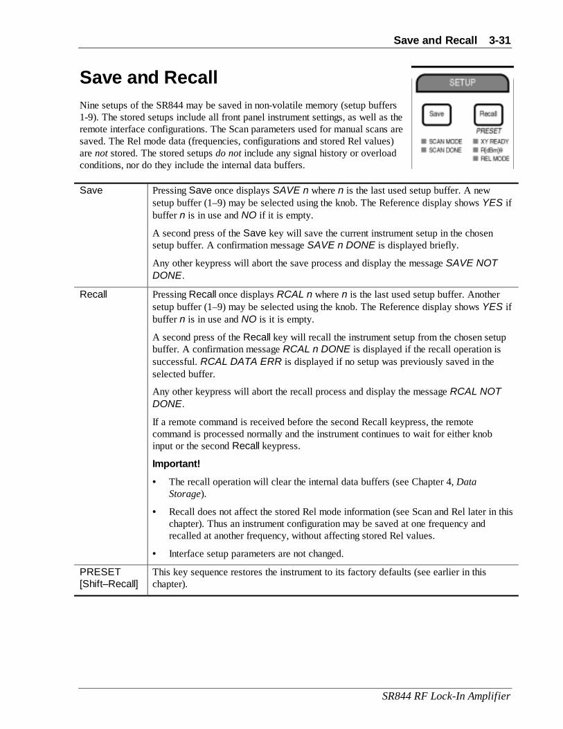
Save and Recall 3-31
SR844 RF Lock-In Amplifier
Save and Recall Nine setups of the SR844 may be saved in non-volatile memory (setup buffers1-9). The stored setups include all front panel instrument settings, as well as theremote interface configurations. The Scan parameters used for manual scans aresaved. The Rel mode data (frequencies, configurations and stored Rel values)are not stored. The stored setups do not include any signal history or overloadconditions, nor do they include the internal data buffers.
Save Pressing Save once displays SAVE n where n is the last used setup buffer. A newsetup buffer (1–9) may be selected using the knob. The Reference display shows YES ifbuffer n is in use and NO if it is empty.
A second press of the Save key will save the current instrument setup in the chosensetup buffer. A confirmation message SAVE n DONE is displayed briefly.
Any other keypress will abort the save process and display the message SAVE NOTDONE.
Recall Pressing Recall once displays RCAL n where n is the last used setup buffer. Anothersetup buffer (1–9) may be selected using the knob. The Reference display shows YES ifbuffer n is in use and NO is it is empty.
A second press of the Recall key will recall the instrument setup from the chosen setupbuffer. A confirmation message RCAL n DONE is displayed if the recall operation issuccessful. RCAL DATA ERR is displayed if no setup was previously saved in theselected buffer.
Any other keypress will abort the recall process and display the message RCAL NOTDONE.
If a remote command is received before the second Recall keypress, the remotecommand is processed normally and the instrument continues to wait for either knobinput or the second Recall keypress.
Important!• The recall operation will clear the internal data buffers (see Chapter 4, Data
Storage).
• Recall does not affect the stored Rel mode information (see Scan and Rel later in thischapter). Thus an instrument configuration may be saved at one frequency andrecalled at another frequency, without affecting stored Rel values.
• Interface setup parameters are not changed.
PRESET[Shift–Recall]
This key sequence restores the instrument to its factory defaults (see earlier in thischapter).

3-32 Interface
SR844 RF Lock-In Amplifier
Interface The SR844 can be interfaced to a host computer via RS232 or GPIB. The keys inthis section configure the interface for proper operation with the host. Theseparameters must be set before attempting to interface the instrument to the hostcomputer.
Setup The Setup key cycles through the remote interface configuration parameters. Indicatorsabove the Setup key indicate which parameter is being shown. The value or setting ofthe parameter is displayed on the Reference Display and is adjusted using the knob. SeeChapter 4, Introduction, for more information about setting the correct interface.
Parameter Configuration NotesGPIB/RS232
The SR844 outputs data to only one interface at a time. Commands maybe received over both interfaces but responses are directed only to theselected interface. Use the knob to select either GPIB or R232 for theoutput interface.
ADDRESS Use the knob to select a GPIB address for the SR844.
BAUD Use the knob to select a RS232 baud rate from 300 to 19200 baud.
PARITY Use the knob to select EVEN, ODD or NONE for the RS232 parity.
QUEUE The last 256 characters received by the SR844 may be displayed to helpfind programming errors. Setup Queue will display 6 hexadecimalcharacters at a time (2 each on the Channel 1, Channel 2 and Referencedisplays). Turn the knob CCW to move farther back in the buffer andCW to move towards the most recently received characters. A period ‘.’is displayed to indicate the ends of the buffer. All characters arechanged to upper-case, spaces are removed, and command delimiters arechanged to linefeeds (0A).
The table below shows the hexadecimal equivalents of all of thecharacters recognized by the SR844.
Hex ASCII Hex ASCII Hex ASCII0A linefeed 39 9 4D M2A * 3B ; 4E N2B + 3F ? 4F O2C , 41 A 50 P2D – 42 B 51 Q2E . 43 C 52 R30 0 44 D 53 S31 1 45 E 54 T32 2 46 F 55 U33 3 47 G 56 V34 4 48 H 57 W

Interface 3-33
SR844 RF Lock-In Amplifier
35 5 49 I 58 X36 6 4A J 59 Y37 7 4B K 5A Z38 8 4C L
LOCAL Remote interface commands can put the SR844 into either the Remote state or the LocalLockout state. It is possible to configure the unit over the remote interface so that thefront panel is inoperative in these states. See in Chapter 4, Interface Commands, forinformation on how to do this. Note that the factory preset values are such that the frontpanel is not disabled by Remote commands.
Attempts to change the settings from the front panel will display the message LOCLLOUT indicating that local control is locked out by the remote interface.
If the unit is in the Remote state and the front panel is locked-out, the Local key willreturn the unit to the Local state and re-enable the front panel. In the Local Lockout state,even the Local key is locked out. It is not possible to distinguish between the Remoteand Local Lockout states from the front panel indicators, since the REMOTE indicator ison in both cases. If the Local key does not return the unit to the Local state, the unit isprobably in the Local Lockout state. There are three ways to get out of the LocalLockout state. One is to turn the power off and back on with the Setup key pressed; thisrestores the factory preset values. The other two methods are by remote commands andare discussed in greater detail in Chapter 4, Interface Commands. LOCL0 takes the unitout of the Local Lockout state, while OVRM1 enables the front panel regardless ofRemote or Local Lockout state.
REMOTE This indicator shows that the SR844 has been put into either the Remote or LocalLockout state by receipt of a remote command. Front panel control may not be allowed.
SRQ This indicator is on when a GPIB service request is generated by the SR844. Thisindicator remains on until a serial poll is completed. See Chapter 4, Status RegisterDefinitions, for more information.
ACTIVE This indicator flashes when there is activity (receive or transmit) on either remoteinterface.
ERROR This indicator flashes when there is a remote interface error, such as an illegal command,or a out-of-range parameter.

3-34 Scan - Rel
SR844 RF Lock-In Amplifier
Scan and Rel
Overview ScansThe SR844 offers the facility of doing a manual frequency scan covering up to 11 frequency points. Thisfacility is available only in the Internal Reference mode. Frequency scans are a convenient method formaking repeated measurements over a set of frequencies. For example, measurements of device noise orfrequency response using REF OUT as the signal source.
The set of scan frequencies are specified by a start frequency, a stop frequency and the number of points.The start frequency and stop frequency may be anywhere within the operating range of the instrument,25 kHz – 200 MHz. The SR844 will select the frequency points by interpolating geometrically betweenthe start and stop frequencies. The following equation gives the frequencies Fi for i=0 to N–1, where N≥2is the number of points.
F FFFi start
stop
start
iN
= ×
−1
Here Fstart and Fstop are the start and stop frequencies respectively. The geometric interpolation isappropriate for wide frequency intervals, and is close to linear for narrow frequency intervals. Theinterpolated frequencies are rounded to the resolution of the internal frequencysource.
The SCAN MODE indicator is on while a scan is in progress. Use the ScanSet key to setup a scan. Scan setup is not permitted while a scan is in progress.Use the Start/Step key to start a scan and to step through the frequencies. Tostop a scan without going through all the frequencies, use OFF (Shift–Scan Set).
RelsAt each scan frequency, a stored measurement setup, or Rel Configuration(sensitivity, reserve, etc.), can be recalled. In addition, stored offsets (Rel Values) may be applied to thesignal. XY Rel Values are stored X and Y offsets. Rθ Rels are stored R[dBm] and θ offsets. Rel Valuescan be stored for each scan frequency.
To store Rel Values at the current scan frequency:
• Use the Store XY key to Auto Offset X and Y and store the offsets as XY Rel offset values. TheXY READY indicator is on when XY Rel Values have been stored at the current scan frequency. Thisalso stores the Rel Configuration (sensitivity, reserve, etc.).
• Use STORE R[dBm]θ (Shift–Store XY) to Auto Offset R[dBm] and Auto Phase the reference andstore the results as R[dBm] and θ Rel offset values. The R[dBm]θθθθ indicator is on when R[dBm]θ RelValues have been stored at the current scan frequency. This also stores the Rel Configuration(sensitivity, reserve, etc.).

Scan - Rel 3-35
SR844 RF Lock-In Amplifier
Use the Rel Mode key to toggle REL MODE on and off.
In SCAN MODE with REL MODE on, the instrument automatically recalls the stored Rel Configurationand Rel Values at each scan frequency. The REL indicator within the CH1 and CH2 displays is onwhenever the recalled Rel Configuration and Rel Values are in effect.
If the current scan frequency does not have any stored Rel Values (as indicated by XY READY orR[dBm]θθθθ), the current configuration and offsets remain in effect. The REL indicator is off in this case.
The stored XY Rel Values are applied as X and Y offsets (adjusted for the current phase). The storedR[dBm] Rel Value is applied as the R[dBm] offset. The stored θ Rel Value is applied as the ReferencePhase (there is no phase offset). Offset indicators within the CH1 and CH2 displays are turned on asappropriate (as well as the REL indicator).
After the Rel Configuration and Rel Values are recalled, the instrument setup can be modified using thefront panel or remote interface. Once the configuration is modified, the REL indicator turns off indicatingthat the current configuration is not the recalled Rel Configuration. Toggle REL MODE off and back on torecall the stored Rel Configuration once again.
When REL MODE is off, stored Rel Configurations and Rel Values are ignored (the configuration andoffsets currently in effect are still applied to the measurement).
Use the CLEAR ALL key (Shift–Rel Mode) to clear all stored Rel Configurations and Values andCLEAR ONE (Shift–Start/Step) to clear the Rels at the current scan frequency only.
Scan and Rel parameters are stored in non-volatile memory and recalled at power on. They are not storedwith the 9 available stored setups.
Using Frequency Scans This section discusses the operation of the frequency Scan Mode. The Scan Mode can be used inconjunction with Rel Mode as described in the following section.
Scan Set This key accesses the scan frequency parameters. Successive keypresses are used tocycle through the Start and Stop frequencies and Number of Points on the ReferenceDisplay. The knob is used at each stage to modify the current parameter.
Changing the scan parameters is not permitted if a scan is in progress (SCAN MODEindicator on). In such a case the knob has no effect. There are three scan parameters:
Parameter DescriptionStart The start frequency, Fstart , is shown on the Reference Display, along with
the START indicator within the display. Use the knob to select a startfrequency in the range 25 kHz – 200 MHz.
Stop The stop frequency Fstop , is shown on the Reference Display, along withthe STOP indicator within the display. Use the knob to select a stopfrequency in the range 25 kHz – 200 MHz.
Number ofPoints
The number of points, N, is shown on the Reference Display. There is noindicator shown in the display. Use the knob to select from 2 to 11 steps.The number of points includes both the start and stop frequencies, so the

3-36 Scan - Rel
SR844 RF Lock-In Amplifier
number of interpolated points is N – 2 .Completing the scan parameter setup procedure does not start a scan. The frequencyreference remains unchanged (Internal or External reference mode) after all scanparameters have been set.
Start/Step This key is used to step through the scan frequencies. If no scan has been setup, thefactory preset values are used, namely Start = 100 kHz, Stop = 100 MHz, N = 4, whichgives interpolated frequencies of 1 MHz and 10 MHz.
The SR844 must be in Internal Reference mode to perform a scan. Start/Step has noeffect unless the unit is in Internal Reference mode.
Successive presses of Start/Step perform the following functions.
Keypress Description1st If a scan is not in progress, pressing the Start/Step key will begin one, if
the SR844 is in Internal reference mode. The frequency is set to the Startfrequency, Fstart , and the SCAN MODE indicator is turned on.
2nd ... Nth Subsequent keypresses step to the next scan frequency, Fi. When thefrequency reaches the Stop frequency, Fstop ,the SCAN DONE indicatorturns on.
N+1st Another keypress exits the Scan Mode while remaining at the Stopfrequency. The SCAN MODE and SCAN DONE indicators both turnoff.
N+2nd The next keypress begins another scan, just like the 1st keypress above.
Important!During a frequency scan, changing some front panel parameters will exit Scan Mode.These are (1) changing the internal frequency and (2) switching to External Referencemode.
OFF
[Shift–Scan Set]
This key sequence terminates Scan Mode. The SCAN MODE and SCAN DONEindicators are turned off. It has no effect if SCAN MODE is off.
Storing and Using Rel Values This section discusses the storage of Rel Values at the scan frequencies. The Scan and Rel features worktogether in a straightforward manner. First, use the Scan keys to specify the frequency scan (Start, Stopand N) as described previously. Then, use Start/Step to step through the scan frequencies while using theStore keys to store Rel Configurations and Values at each frequency. Changing scan parameters clears allstored Rels.
XY Rel Values are actually stored X and Y offsets. Rθ Rel Values are stored offsets for R[dBm] andstored settings of the reference phase. Rel Values are stored along with the current measurementconfiguration. This is because offsets are generally valid only for a specific configuration and are not

Scan - Rel 3-37
SR844 RF Lock-In Amplifier
appropriate for different configurations. Using stored Rel Values at a scan frequency will alsorecall the stored measurement configuration.
The measurement configuration includes:
• Signal Z-In • Sensitivity• Wide Reserve • Close Reserve• Phase (if Rθ Rel Values are stored) • Ratio• Time Constant Slope (but not the Time Constant)
Other parameters, such as Display, Expand and AUX OUT values are not included.
Press Rel Mode to turn REL MODE on. In this mode, stored Rel Configurations and Values areautomatically recalled at the current scan frequency (if previously stored, as indicated by XY READY orR[dBm]θθθθ). When a Rel Configuration is recalled, the REL indicators within the CH1 and CH2 displaysare turned on. The XYOffs and ROffs indicators within the displays are turned on and off as appropriate.
After a Rel Configuration is recalled, changing the measurement configuration or modifying offsets causesthe REL indicators to turn off. This does not alter the stored Rel Values or Configuration, it merelyindicates that the current configuration is not the same as the stored configuration. It also does not alter theoffsets currently in use. Use Rel Mode to toggle REL MODE off and back on to recall the stored RelValues and Configuration once again.
Changing frequency scan parameters clears all stored Rel Values. Use the CLEAR ALL key (Shift–RelMode) to clear all stored Rel Configurations and Values and CLEAR ONE (Shift–Start/Step) to clearthe Rels at the current scan frequency only.
The Rel Values are saved when the instrument power is turned off. They are not stored with the 9available stored setups.
Store XY Performs Auto Offset on both X and Y and stores the XY offsets as XY Rel Values atthe current scan frequency. X and Y displays and outputs are offset to zero. Anypreviously stored XY Rel Values are replaced. The current measurement configuration isalso saved. Previously stored Rθ Rel Values are discarded if they were stored with ameasurement configuration which differs from the current one.
The XY READY indicator turns on indicating that XY Rel Values are stored for thisscan frequency.
StoreR[dBm]θ
[Shift–Store XY]
Performs Auto Phase and Auto Offset on R[dBm] and stores the R[dBm] offset andreference phase as Rθ Rel Values at the current scan frequency. R[dBm] and θ displaysare offset to zero. Any previously stored Rθ Rel Values are replaced. The currentmeasurement configuration is also saved. Previously stored XY Rel Values arediscarded if they were stored with a measurement configuration which differs from thecurrent one.
The R[dBm]θθθθ indicator turns on indicating that Rθ Rel Values are stored for this scanfrequency.

3-38 Scan - Rel
SR844 RF Lock-In Amplifier
XY READYR[dBm]θθθθ
These indicators are on if there are XY or Rθ Rel Values stored for the current scanfrequency. They do not imply that these Rel Values are being applied to the currentmeasurement.
Rel Mode This key toggles REL MODE.
In SCAN MODE with REL MODE on, the instrument automatically recalls the storedRel Configuration and Rel Values at each scan frequency (if previously stored, asindicated by XY READY or R[dBm]θθθθ). The REL indicator within the CH1 and CH2displays is on whenever the recalled Rel Configuration and Rel Values are in effect.
If the current scan frequency does not have any stored Rel Values (as indicated byXY READY or R[dBm]θθθθ), the current configuration and offsets remain in effect. TheREL indicator is off in this case.
The stored XY Rel Values are applied as X and Y offsets (adjusted for the currentphase). The stored R[dBm] Rel Value is applied as the R[dBm] offset. The stored θ RelValue is applied as the Reference Phase (there is no phase offset). Offset indicatorswithin the CH1 and CH2 displays are turned on as appropriate (as well as the RELindicator).
Turning REL MODE off does not change the current measurement. The currentmeasurement configuration remains in effect. As long as REL MODE is off, stored RelValues and Configurations are not recalled at any other scan frequencies.
CLEAR ALL[Shift–RelMode]
This key sequence discards all stored Rel Values and Configurations.
CLEAR ONE[Shift–Start/Step]
This key sequence discards the stored Rel Values and Configurations at the current scanfrequency.
Any key thatchanges theinstrumentconfiguration
All keys in the SIGNAL INPUT and SENSITIVITY sections as well as SlopeUp/Down, Ratio, Recall, Preset, Ref Z-In, Ref Source change the measurementconfiguration and turn the REL indicators off. This does not affect REL MODE.
Start/Step This key is used to step through the scan frequencies. If REL MODE is on, stored RelConfigurations and Values (if previously stored) will be applied.

Scan - Rel 3-39
SR844 RF Lock-In Amplifier
Scan and Rel Example In this example we will make transfer function measurements of a device–under–test, or DUT, using theSR844 REF OUT signal in Internal Reference mode. For this example, we assume that the DUT attenuatesthe REF OUT signal. We will make measurements at several frequencies using the Scan Mode. We willuse Rel Mode to store the measured values when the DUT is by-passed (using STORE R[dBm]θ).
First, we set the frequency scan parameters to select the scan frequencies. Then we step through the scanwith the DUT by-passed, storing Rel Configurations and Values at each frequency (usingSTORE R[dBm]θ). This measures the DUT input. Next we pass the signal through the DUT and stepthrough the frequency scan again. This measures the transfer response of the DUT directly in dB anddegrees.
If the DUT amplifies the signal, we would need to make the scan with the DUT in the signal path first,storing Rel Values and Configurations. The second scan by-passes the DUT and measures the transferresponse (negate both the dB and phase readings). The order is determined by which configuration(through the DUT or by-pass the DUT) has the larger output signal. This determines the requiredmeasurement configuration at each frequency.
1 Connect the REF OUT signal (appropriately attenuated and terminated) to the input of the DUT. TheDUT output should be connected to the SIGNAL IN of the SR844.
Now by-pass the DUT, leave as much of the apparatus in place as possible. It is important to use thesame cabling for both setups (by-pass and through the DUT) in order to preserve phase delaysthrough the system.
2 Set the frequency scan parameters using the Scan Set key and knob as described previously in thesection Using Frequency Scans. Press CLEAR ALL [Shift– Rel Mode] to discard any previouslystored Rel Values.
3 Press Start/Step once to begin/continue the frequency scan.
4 Adjust the instrument configuration to measure the signal appropriately. Set the displays to showR[dBm] on CH1 and θ on CH2. This measures the DUT input.
5 Press STORE R[dBm]θ. This saves the signal phase and the measured value of R[dBm] as well asthe measurement configuration to be used in the next scan.
6 Repeat steps 3–5 until the Scan is done.
7 Now pass the signal through the DUT.
8 Press Start/Step once more to turn Scan Mode off at the Stop frequency.
9 Press Rel Mode to turn on REL MODE and use the stored Rel Values. The next scan will displayR[dBm] and phase relative to the original scan taken with the DUT by-passed. This is exactly thetransfer function we started out to measure.
10 Press Start/Step once to begin/continue the frequency scan.
11 When the measurement is stable, note the readings. In dB and degrees, these give the value of thetransfer function of the DUT at the current frequency.
12 Repeat steps 10–11 until the Scan is done.

3-40 Scan - Rel
SR844 RF Lock-In Amplifier
Rels without Scan This section discusses the storage of Rel Values when the unit is not in Scan mode. This is useful forexternal reference configurations or for frequency points that are not in a log series. Up to 11 different RelConfigurations may be stored (at 11 different frequencies).
To store Rel Values at the current frequency:
• Use the Store XY key to Auto Offset X and Y and store the offsets as XY Rel offset values. TheXY READY indicator is on when XY Rel Values have been stored at the current frequency. This alsostores the Rel Configuration (sensitivity, reserve, etc.).
• Use STORE R[dBm]θ (Shift–Store XY) to Auto Offset R[dBm] and Auto Phase the reference andstore the results as R[dBm] and θ Rel offset values. The R[dBm]θθθθ indicator is on when R[dBm]θ RelValues have been stored at the current frequency. This also stores the Rel Configuration (sensitivity,reserve, etc.).
Use the Rel Mode key to toggle REL MODE on and off.
With REL MODE on, the instrument automatically recalls the stored Rel Configuration and Rel Valueswhenever the frequency is within 1% of a frequency for which a Rel Configuration and Values has beenstored. The REL indicator within the CH1 and CH2 displays is on whenever the recalled RelConfiguration and Rel Values are in effect.
If the current frequency does not have any stored Rel Values (as indicated by XY READY or R[dBm]θθθθ),the current configuration and offsets remain in effect. The REL indicator is off in this case.
The stored XY Rel Values are applied as X and Y offsets (adjusted for the current phase). The storedR[dBm] Rel Value is applied as the R[dBm] offset. The stored θ Rel Value is applied as the ReferencePhase (there is no phase offset). Offset indicators within the CH1 and CH2 displays are turned on asappropriate (as well as the REL indicator).
After the Rel Configuration and Rel Values are recalled, the instrument setup can be modified using thefront panel or remote interface. Once the configuration is modified, the REL indicator turns off indicatingthat the current configuration is not the recalled Rel Configuration. Toggle REL MODE off and back on torecall the stored Rel Configuration once again.
When REL MODE is off, stored Rel Configurations and Rel Values are ignored (the configuration andoffsets currently in effect are still applied to the measurement).
• Pressing CLEAR ALL clears all stored Rel Configurations, both those stored with a scan and thosestored at specific frequencies.
• Pressing the CLEAR ONE clears the Rel Configuration stored with the current frequency (if any).
• The Rel Configurations are indexed by frequency with a 1% tolerance band. Rels stored at 90.0MHzwill be recalled whenever the frequency falls between 89.1MHz (-1%) and 90.9MHz (+1%).
• You should familiarize yourself with the preceding sections before using the Rels without Scan.
Auto Functions 3-41
SR844 RF Lock-In Amplifier
Auto Functions WideReserve
Shift–WideResrvDown
Select the Wideband Dynamic Reserve mode automatically. This functionwill execute once when the keys are pressed. A tone sounds when thefunction is complete. The reserve will not continue to change even if theinput signal changes substantially. To adjust for the changed conditions, itmay be necessary to perform the Auto function again, or make manualchanges. The Wide Reserve AUTO indicator is on while this functionexecutes.
CloseReserve
Shift–CloseResrv
Select the Close Dynamic Reserve mode automatically. This function willexecute once when the keys are pressed. A tone sounds when the function iscomplete. The reserve will not continue to change even if the input signalchanges substantially. To adjust for the changed conditions, it may benecessary to perform the Auto function again, or make manual changes. TheSensitivity AUTO indicator is on while this function executes.
Sensitivity Shift–SensUp
Automatically adjust the sensitivity based on the detected signal magnitude,instrument reserve settings and overload conditions. This function executesonce when the keys are pressed. A tone sounds when the function iscomplete. The sensitivity will not continue to change even if there is asubstantial change in the input signal. In the case of a substantial signalchange, it may be necessary to perform the Auto Sensitivity function again,or adjust the sensitivity/reserve manually. Auto Sensitivity takes more timeto complete at larger time constants. The Sensitivity AUTO indicator is onwhile Auto Sensitivity is in progress.
Auto Sensitivity will not execute if the time constant is greaterthan 1 s.
Phase Shift–Phase Select the Reference Phase that matches the phase of the input signal. A tonesounds when the function is complete. This results in a measured phase ofthe input signal that is close to zero. If the measured phase of the inputsignal is not settled or is noisy at the time Shift-Phase is pressed, themeasured phase may not settle to 0°.
Auto phase is executed once at the time the keys are pressed. The ReferencePhase will not track changes in the phase of the input signal. However the Rfunction always provides the magnitude of the input signal, even as thephase moves, as long as the phase moves slowly compared to themeasurement time constant.
Offset CH1 or CH2Offset Auto
This key sets the Offset for the displayed quantity equal to the negative ofits current value, so that the display, with offset applied, is equal to zero.The Offset is turned On if it is not already On. This key has no effect forquantities that may not be offset.
Important!If the display is X or Y, Auto Offset is performed on both X and Y and turnson both X and Y offsets. This is true even if the other display is notdisplaying X or Y at the time.

3-42 Shift Functions
SR844 RF Lock-In Amplifier
Shift Functions Some keys have shift functions labeled in blue below the key.
SETTLE... Shift–TimeConstant Up
This key sequence causes the Reference Display to show the elapsedtime (in units of the current Time Constant).
PRESET Shift–Recall This key sequence restores the instrument to its factory defaults (seeearlier in this chapter).
–90° [Shift– +90°] This key sequence changes the reference phase by –90°.
I.F. [Shift– AuxOut] This key sequence shows the IF frequency on the Reference Display.See Chapter 2, Sources of Error, for more information about the IF(chop frequency). This display is provided as a user convenience.The instrument has weak spurious responses at offsets of ±2×IF,±4×IF, etc. from the reference frequency. Some users may wish to setup their experiments to avoid specific IF frequencies.
When the reference is in internal mode and the IF frequency isdisplayed, the knob may be used to adjust the internal referencefrequency while showing the IF frequency.
Important!The SR844 covers the operating frequency range in octave bands.Users can check the IF frequency to determine whether the instrumentis at the high end of an octave band or the low end of the next band.At the high end of an octave, the IF frequency will be close to 3 kHz(12 kHz for time constants ≤300 µs), while at the low end it will beclose to 2 kHz (8 kHz for time constants ≤300 µs). The IF frequencyaffects the output update rate for the analog CH1/CH2 OUTPUTs.The fastest update rates occur at the high end of each octave band(where the IF is the highest).
PRECISEFREQ
[Shift– Freq] This key sequence shows the reference frequency with 6 or 7 digitsresolution using the CH2 and Reference displays together. Read thetwo displays as if they were one single display. While the internalreference frequency is set to 3 digits resolution, the actual frequencygenerated in internal mode may be slightly different (within ±1 in the4th digit).
To cancel this display mode, choose another reference display (Freqor Phase for example).
Null [Shift–Shift] A second keypress cancels the first Shift if it is pressed by mistake.
OFF [Shift–Scan Set]
This key sequence terminates Scan Mode. It has no effect if SCANMODE is off.
CLEAR ALL [Shift–RelMode]
This key sequence discards all stored Rel Configurations and Values.

Shift Functions 3-43
SR844 RF Lock-In Amplifier
CLEAR ONE [Shift–Start/ Step]
This key sequence discards the stored Rel Configurations and Valuesat the current frequency.
STORER[dBm]θ
[Shift–Store XY]
Performs Auto Phase and Auto Offset on R[dBm] and stores theR[dBm] offset and reference phase as Rθ Rel Values at the currentscan frequency. R[dBm] and θ displays are offset to zero. Anypreviously stored Rθ Rel Values are replaced. If the currentmeasurement configuration differs from the previously storedconfiguration, it is also replaced. Previously stored XY Rel Valuesare discarded if they were stored with a measurement configurationwhich differs from the current one.
The R[dBm]θθθθ indicator turns on indicating that Rθ Rel Values arestored for this scan frequency.
2F Mode [Shift–Source] This key sequence toggles 2F harmonic detection. 2F mode is shownby the indicator above the EXTERNAL and INTERNAL indicators.
2F detection is available for both External and Internal Referencemodes. In both cases, the displayed frequency is the 2F detectionfrequency. The frequency of the REF OUT signal is at F or half of thedisplayed detection frequency. In External mode, the frequencies ofREF IN and REF OUT are both F.
Important!The 2F detection frequency is limited to 50 kHz to 200 MHz. Thiscorresponds to a REF IN and REF OUT frequency range of 25 kHz to100 MHz.
The absolute phase in 2F mode is not specified. However, the relativephase accuracy generally applies.

3-44 Shift Functions
SR844 RF Lock-In Amplifier

4-1
SR844 RF Lock-In Amplifier
Chapter 4
Remote Operation
In This Chapter Index of Commands 4-2
Introduction 4-7Communicating With GPIB 4-7Communicating With RS232 4-7Indicators 4-7Queues 4-7Command Format 4-8Command Synchronization 4-8Example Program 4-9
Command Syntax 4-10Output Interface (RS232 or GPIB) 4-10Reference and Phase Commands 4-11Signal Input Commands 4-12Gain and Time Constant Commands 4-13Display and Output Commands 4-15Aux Input and Output Commands 4-17Setup Commands 4-18Auto Functions 4-20Scan and Rel Functions 4-21Data Storage 4-22Data Storage Commands 4-24Data Transfer Commands 4-25Interface Commands 4-29Status Reporting Commands 4-30
Status Register Definitions 4-31Using Serial Poll 4-32Using *STB? 4-33Using Status Enable Registers 4-33Service Requests (SRQ) 4-33
Example Program 4-34Using Microsoft C with the GPIB interface 4-34

4-2 Index of Commands
SR844 RF Lock-In Amplifier
Index of Commands Variablesch output channel (1=CH1, 2=CH2)i,j,k,l,m,n,q integersf real number frequency in Hzx,y,z real numbers
Syntax(?) required for queries only - illegal for setvar always requiredvar required for sets only - illegal for query[var] optional for set and query
Reference and PhaseFMOD(?)i 4-11 Set (Query) the Reference Mode to External (0) or Internal (1).HARM(?)i 4-11 Set (Query) the 2F detect Mode to Off (0) or On (1).FREQ(?)f 4-11 Set (Query) the Reference Frequency to f Hz. Set allowed only in
Internal Reference mode.FRAQ? 4-11 Query the Reference Frequency to 6 or 7 digits precision in Hz.FRIQ? 4-11 Query the IF frequency. Returns an integer number of Hz.PHAS(?)x 4-11 Set (Query) the Reference Phase to x degrees.APHS 4-20 Perform AutoPhase function.REFZ(?)i 4-11 Set (Query) the Reference Input impedance to 50 Ω (0) or 10 kΩ (1).
Signal InputWRSV(?)i 4-12 Set (Query) the Wide Reserve Mode to High Reserve (0), Normal (1), or
Low Noise (2).AWRS 4-20 Automatically set Wide Reserve Mode.INPZ(?)i 4-12 Set (Query) the Signal Input Impedance to 50 Ω (0) or 1 MΩ (1).
Gain and Time ConstantSENS(?)i 4-13 Set (Query) the Sensitivity to 100 nV (0) through 1 V (14) rms full-
scale.AGAN 4-20 Perform Auto Sensitivity.CRSV(?)i 4-13 Set (Query) the Close Dynamic Reserve Mode to High Reserve (0),
Normal (1) or Low Noise (2).ACRS 4-20 Automatically set Close Reserve Mode.OFLT(?)i 4-13 Set (Query) the Time Constant to 100µs (0) through 30 ks (17).OFSL(?)i 4-13 Set (Query) the Time Constant Filter Slope to 6 (i=1), 12 (2), 18 (3),
24 (4) dB/oct, or NoFilter Mode (i=0).SETL(?) 4-14 Reset Elapsed Time counter to zero, return elapsed T.C.’s.

Index of Commands 4-3
SR844 RF Lock-In Amplifier
Display and OutputDDEF(?)ch,q 4-15 Set (Query) the CH1 (ch=1) display to X (q=0), R[V] (1), R[dBm] (2),
Xn (3), AuxIn1 (4) or CH2 (ch=2) to Y (q=0), θ (1), Yn[V] (2),Yn[dBm] (3), AuxIn2 (4).
DRAT(?)i 4-15 Set (Query) the Ratio Mode to Off (0), ÷AuxIn1 (1), ÷AuxIn2 (2).FPOP(?)ch,i 4-15 Set (Query) the CH1/CH2 analog output to Display (0) or X/Y (1).DOFF(?)
ch,q,x4-15 Set (Query) the CH1/CH2 Offset for X, R[V], R[dBm] or Y to x % full
scale.AOFF ch,q 4-20 Auto Offset CH1/CH2 for X, R[V], R[dBm] or Y.DEXP(?)
ch,q,i4-16 Set (Query) the Expand for X, R[V], R[dBm], Xn, Y, θ, Yn [V] to
×1 (i=0), ×10 (1), ×100 (2).
Aux Input and OutputAUXI? i 4-17 Query the value of Aux Input i (1 or 2).AUXO(?)i,x 4-17 Set (Query) the value of Aux Output i (1 or 2) to x Volts.
SetupOUTX(?)i 4-18 Set (Query) the Output Interface to RS-232 (0) or GPIB (1).OVRM(?)i 4-18 Set (Query) the GPIB Override Remote mode to Off (0) or On (1).KCLK(?)i 4-18 Set (Query) the Keyclick to Off (0) or On (1).ALRM(?)i 4-18 Set (Query) the Alarms to Off (0) or On (1).SSET i 4-18 Save current settings to Buffer i (1–9).RSET i 4-18 Recall settings from Buffer i (1–9).KNOB i 4-18 Execute i knob adjustments.KEYP i 4-18 Press key i.
Auto FunctionsAWRS 4-20 Automatically set Wideband Reserve Mode.ACRS 4-20 Automatically set Close-In Reserve ModeAGAN 4-20 Perform AutoGain to set the Sensitivity.APHS 4-20 Perform AutoPhase to get X=maximum positive and Y=0.AOFF ch,q 4-20 AutoOffset X, R[V], R[dBm] only.
Scan and RelSSTR(?)f 4-21 Set (Query) the Scan Start Frequency to f Hz.SFIN(?)f 4-21 Set (Query) the Scan Stop Frequency to f Hz.SSTP(?)i 4-21 Set (Query) the Scan Number of Points to 2 ≤ i ≤ 11.SMOD(?)i 4-21 Set (Query) the current Scan Point (1 ≤ i ≤ N) or Off (0).RSTO i 4-21 Store XY (1), or R[dBm]θ (2) Rel Values.RRDY? i 4-21 Query Rels Ready XY (1) or R[dBm]θ (2) returns 0 (no) or 1 (yes).RCLR 4-21 Clear all stored Rel Values and Configurations.RMOD(?)i 4-21 Query Rel/Lock on (1) or off (0).

4-4 Index of Commands
SR844 RF Lock-In Amplifier
Data StorageSRAT(?)i 4-24 Set (Query) the Data Sample Rate to 62.5 mHz (0) through 512 Hz (13)
or Trigger (14).SEND(?)i 4-24 Set (Query) the End of Scan mode to One–Shot (0) or Loop (1).TRIG 4-24 Sample trigger command. Same as trigger input.TSTR(?)i 4-24 Set (Query) the Trigger Starts Scan mode to No (0) or Yes (1).STRT 4-24 Start or continue a scan.PAUS 4-24 Pause during a scan. Does not reset a paused or done scan.REST 4-24 Reset the scan. All stored data is lost.
Data TransferOUTP?i 4-25 Query the value of X (1), Y (2), R[V] (3), R[dBm] (4) or θ (5).OUTR?ch 4-25 Query the value of Display ch (1,2).SNAP?i,j,k,l,
m,n4-25 Query the value of 2 to 6 parameters simultaneously.
SPTS? 4-26 Query the number of points stored in the Display buffer.TRCA? ch,j,k 4-26 Read k≥1 points starting at bin j≥0 from Display ch (1,2) buffer in
ASCII floating point.TRCB? ch,j,k 4-26 Read k≥1 points starting at bin j≥0 from Display ch (1,2) buffer in
IEEE binary floating point.TRCL? ch,j,k 4-27 Read k≥1 points starting at bin j≥0 from Display ch (1,2) buffer in
non-normalized binary floating point.FAST(?)i 4-28 Set (Query) Fast Data Transfer mode to Off (0) or On(1). Fast mode
will transfer binary X and Y every sample during a scan over GPIB.STRD 4-28 Start a Scan after 0.5 s delay. Use with Fast Data Transfer mode.
Interface*RST 4-29 Reset the SR844 to its default configuration.PRST 4-29 Power-On reset of SR844.*IDN? 4-29 Read the SR844 device identification string.LOCL(?)i 4-29 Set (Query) the Local/Remote state to Local (0), Remote (1) or Local
Lockout (2).OVRM(?)i 4-29 Set (Query) the Override Remote mode to Off (0) or On (1).
Status*CLS 4-30 Clear all status bytes.*STB?[i] 4-30 Query the Serial Poll Status Byte. If i is included only bit i is queried.*SRE(?)[i,]j 4-30 *SREj sets the Serial Poll Enable Register to the decimal value j (0–
255). *SREi,j sets bit i (0–7) to j (0,1). *SRE? queries theentire register. *SRE?i queries bit i.
*ESR?[i] 4-30 Query the Standard Event Status Byte. If i is included only bit i isqueried.
*ESE(?)[i,]j 4-30 *ESEj sets the Standard Event Status Enable Register to decimal valuej (0–255). *ESEi,j sets bit i (0–7) to j (0,1). *ESE? queriesthe entire register. *ESE?i queries bit i.
*PSC(?)i 4-30 Set (Query) the Power–On Status Clear bit to Set (1) or Clear (0).

Index of Commands 4-5
SR844 RF Lock-In Amplifier
ERRS?[i] 4-30 Query the Error Status Byte. If i is included only bit i is queried.ERRE(?)[i,]j 4-30 ERREj sets the Error Status Enable Register to decimal value j (0–
255). ERREi,j sets bit i (0–7) to j (0,1). ERRE? queries theentire register. ERRE?i queries bit i.
LIAS?[i] 4-30 Query the LIA Status Register. If i is included only bit i is queried.LIAE(?)[i,]j 4-30 LIAEj sets the LIA Status Enable Register to decimal value j (0–
65535). LIAEi,j sets bit i (0–15) to j (0,1). LIAE? queries theentire register. LIAE?i queries bit i.
Serial Poll Status: *STB?, *SRE Error Status: ERRS?, ERREbit name set when... bit name set when...0 SCN No data is being stored. 0 –– unused1 IFC No command in progress. 1 BAK Battery backup failed.2 ERR Enabled bit in Error status set. 2 RAM RAM memory test failed.3 LIA Enabled bit in LIA status set. 3 FPG FPGA test failed.4 MAV Interface output buffer not empty. 4 ROM ROM memory test failed.5 ESB Enabled bit in Standard Event
status set.5 GPB GPIB Fast Data Transfer aborted.
6 SRQ Service Request has occurred. 6 DSP DSP test failed.7 –– unused 7 MTH Internal math error occurred.
Standard Event Status: *ESR?, *ESE LIA Status: LIAS?, LIAE
bit name set when... bit name set when...0 RXQ Input queue overflows. 0 ULK Reference unlocked.1 –– unused 1 FRQ Ext Ref frequency out of range.2 TXQ Output queue overflows. 2 –– unused3 –– 3 TRG Data storage triggered.4 EXE Command execution error occurs. 4 INP Signal Input overloads.5 CMD Illegal command received. 5 RSV IF amplifier overloads.6 URQ Any key–press or knob rotation. 6 FLT Time constant filter overloads.7 PON Power–on. 7 CHG Ref frequency changed by >1%.
8 CH1 CH1 display or front panel ovld.9 CH2 CH2 display or front panel ovld.
10 OAX Aux input overflows.11 UAX Aux input underflows.

4-6 Index of Commands
SR844 RF Lock-In Amplifier

Remote Operation 4-7
SR844 RF Lock-In Amplifier
Introduction The SR844 RF Lock-In Amplifier may be remotely programmed via either the RS232 orGPIB (IEEE-488) interfaces. Any computer supporting one of these interfaces may beused to program the SR844. Both interfaces are receiving at all times, however, the SR844will send responses to only one interface. Specify the output interface with the OUTXcommand at the start of every program.
Important!Use the OUTX command at the beginning of every program to direct theSR844 responses to the correct interface.
Communicating With GPIB The SR844 supports the IEEE-488.1 (1978) interface standard. It also supports therequired common commands of the IEEE-488.2 (1987) standard. Before attempting tocommunicate with the SR844 over the GPIB interface, the SR844's Device Address mustbe set with the Setup key.
Communicating With RS232 The SR844 is configured as a DCE ( transmit on pin 3, receive on pin 2) device andsupports CTS/DTR hardware handshaking. The CTS signal (pin 5) is an output indicatingthat the SR844 is ready, while the DTR signal (pin 20) is an input that is used to controlthe SR844's data transmission. If desired, the handshake pins may be ignored and a simple3 wire interface (pins 2, 3 and 7) may be used. The RS232 interface Baud Rate and Parityare set with the Setup key. The RS232 word length is always 8 bits.
Indicators To assist in programming, the SR844 has four interface status indicators located in theINTERFACE section of the front panel.
The ACTIVE indicator flashes whenever a character is received or transmitted over eitherinterface.
The ERROR indicator flashes when an error, such as illegal command, or parameter outof range, has been detected.
The REMOTE indicator is on whenever the SR844 is in the Remote state (front panelmay be locked out).
The SRQ indicator is on when the SR844 generates a service request. SRQ stays onuntil a GPIB serial poll is completed.
Queues To help find program errors, the SR844 can display its receive buffer on the displays. Usethe Setup key to access the Queue display. The last 256 characters received by theSR844 may be displayed in hexadecimal format. See the Chapter 3, Interface, for acomplete description.

4-8 Remote Operation
SR844 RF Lock-In Amplifier
Command Format Communication with the SR844 uses ASCII characters. Commands may be in eitherUPPER or lower case and may contain any number of embedded SPACE characters. Acommand to the SR844 consists of a four character command mnemonic with optional ?,arguments if necessary, and a command terminator. The command, arguments andterminator may be separated by spaces. The terminator must be a linefeed <LF> orcarriage return <CR> on RS232, or a linefeed <LF> or EOI on GPIB. No commandprocessing occurs until a terminator is received. Commands function identically on GPIBand RS232 whenever possible. Command mnemonics beginning with an asterisk ‘*’ areIEEE-488.2 (1987) defined common commands. These commands also functionidentically on RS232. Commands may require one or more parameters. Multipleparameters are separated by commas (,).
Multiple commands may be sent on one command line by separating them withsemicolons (;).
There is no need to wait between commands. The SR844 has a 256 character input bufferand processes commands in the order received. If the buffer fills up, the SR844 will holdoff handshaking on the GPIB and attempt to hold off handshaking on RS232. Similarly, theSR844 has a 256 character output buffer to store output until the host computer is readyto receive it. If either buffer overflows, both buffers are cleared and an error reported.
The present value of a particular parameter may be determined by querying the SR844 forits value. A query is formed by appending a question mark ‘?’ to the command mnemonicand omitting the desired parameter from the command. Values returned by the SR844 aresent as a string of ASCII characters terminated by a carriage return <CR> on RS232 andby a line-feed <LF> on GPIB. If multiple query commands are sent on one command line(separated by semicolons, of course), the answers will be returned individually, each witha terminator.
Examples of CommandsFMOD 1 <LF> Set Reference Mode to InternalFREQ 27E5 <LF> Set the internal reference frequency to 27E5 Hz (2.7 MHz)*IDN? <LF> Query the device identificationSTRT <LF> Start internal data storageOUTP? 1 <LF> Query the value of X
Command Synchronization IFC (Interface Ready, bit 1) in the Serial Poll status signals that the SR844 is ready toreceive and execute a command. When a command is received, this bit is cleared,indicating that command execution is in progress. No other commands will be processeduntil this command is completed. Commands received during this time are stored in thebuffer to be processed later. Only GPIB serial polling will generate a response while acommand is in progress. When all pending commands have executed, the IFC bit is setagain. By checking IFC with serial polls, a host computer can ensure that all previouslysent commands have finished before sending a new command.

Remote Operation 4-9
SR844 RF Lock-In Amplifier
Since most commands execute very quickly, the host computer does not need tocontinually check the IFC bit. Commands may be sent one after another and they will beprocessed immediately.
However, some commands, such as reset and auto–function commands, may require along time to execute. In addition, the host program may need to check that theseoperations executed without error. In these cases, after the command is sent, the statusshould be queried.
When using the GPIB interface, serial polling may be used to check the IFC bit in theSerial Poll status while an operation is in progress. After the IFC bit becomes set,signaling the completion of the command, then the ERR or ESB bits may be checked toverify successful completion of the command.
If the RS232 interface is used, or serial polling is not available, then the *STB? querycommand may be used to read the Serial Poll status word. However, *STB? neverreturns the IFC bit set (since *STB? is itself a command).
Since the SR844 processes one command at a time, status queries will not be processeduntil the previous operation is finished. Thus a response to a status query in itself signalsthat the previous command is finished. The query response may then be checked forvarious errors.
Example Program An example program is included at the end of this chapter. This program is a goodreference for writing your own programs to control the SR844.

4-10 Remote Operation
SR844 RF Lock-In Amplifier
Command Syntax The four letter mnemonic (shown in CAPS) in each command sequence specifies thecommand. The rest of the sequence consists of parameters. Parameters shown in and[ ] are not always required. Generally, parameters in are required to set a value in theSR844 and parameters in [ ] are optional in both set and query commands. Multipleparameters are separated by commas. Multiple commands may be sent on one commandline by separating them with semicolons (;).
The present value of a parameter may be determined by sending a query command.Commands that may be queried have a question mark in parentheses (?) after themnemonic. Commands that may ONLY be queried have a ? after the mnemonic.Commands that MAY NOT be queried have no ?. A query is formed by including thequestion mark ? after the command mnemonic and omitting the queried parameter fromthe command. The query parameters shown in are NOT sent with a query. The queryreturns the value of these parameters. Values are returned as a string of ASCII characters(unless otherwise noted).
Do not send ( ) or or [ ] as part of the command.
For example, the command AUXO (?) i ,x is used as follows.
AUXO 1,1.234 Set AUX OUT 1 to 1.234 VAUXO? 1 Query the current setting of AUX OUT 1
Variables are defined as follows.
ch output channel (1=CH1, 2=CH2)i,j,k,l,m,n,q integersx,y,z real numbersf real number frequency in Hzs text string
All numeric variables may be expressed in integer, floating point or exponential formats(i.e., the number five can be either 5, 5.0, or 0.5E1). Strings are sent as a sequenceof ASCII characters.
Output Interface (RS232 or GPIB) All responses are directed only to the selected output interface. Use the OUTXcommand at the beginning of every program to select the correct interface.

Reference and Phase 4-11
SR844 RF Lock-In Amplifier
Reference and Phase Commands FMOD(?)i The FMOD command sets or queries the Reference Mode. The parameter i
selects Internal (i=1) or External (i=0) reference.
HARM(?)i The HARM command sets or queries 2F detect mode. The parameter i selectsOFF, (detect at F, i=0) or ON, (detect at 2F, i=1).
The 2F detect frequency is limited to 50 kHz to 200 MHz. The HARM 1 commandwill generate an error if the Reference Mode is Internal and the referencefrequency is below 50 kHz. The HARM 1 command will result in an OUT OFRANGE indication if the Reference Mode is External and the REF IN frequencyis below 25 kHz.
FREQ(?)f The FREQ command sets or queries the detection (reference) frequency. When 2Fmode is Off, the detection frequency is the same as REF IN and REF OUT. When2F mode is On, the detection frequency is twice REF IN and REF OUT.
The FREQ? query will return the detection frequency in Internal or External mode.In Internal mode the frequency is returns the displayed reference frequency (3 digitresolution), whereas in External mode frequency is returned to the measurementresolution (6 or 7 digits). The instrument measures the frequency at 6–12 times asecond.
The FREQ f command sets the frequency of the internal reference oscillator. Thiscommand is allowed only if the Reference Mode is Internal. The parameter f is areal number that specifies the frequency in Hz. The value of f will be rounded tothe nearest available internal frequency. The value of f must be in the range 2.5E4≤ f ≤ 2.0E8 (2F Off) and 5.0E4 ≤ f ≤ 2.0E8 (2F On)
FRAQ? The FRAQ? command queries the reference frequency. The frequency is returnedwith the measurement resolution (6 or 7 digits) in both External and Internal mode.
FRIQ? The FRIQ? command queries the IF frequency. The returned value is an integerwith units of Hz.
The IF frequency will be in the range of approximately 2–3 kHz, for all timeconstants 1 ms and longer. The SR844 uses a higher IF, approximately 8–12 kHz,for faster time constants.
PHAS(?)x The PHAS command sets or queries the detection phase, in degrees, relative to thereference. The parameter x is the phase (real number of degrees) and may bespecified from –360 ≤ x ≤ 360. The value specified is rounded to 0.01° andadjusted to the interval [-179.99 , 180.00 ].
APHS The APHS command performs the Auto Phase function. This command is the sameas pressing Shift−Phase. This command adjusts the reference phase so that thecurrent measurement has a Y value of zero and an X value equal to the signalmagnitude, R.
REFZ(?)i The REFZ command sets or queries the Reference Input impedance. Theparameter i selects 50 Ω (i=0) or 10 kΩ (i=1).

4-12 Signal Input
SR844 RF Lock-In Amplifier
Signal Input Commands WRSV(?)i The WRSV command sets or queries the Wide Reserve Mode of the instrument.
The parameter i selects High Reserve (i=0), Normal (i=1), or Low Noise(minimum wide reserve) (i=2).
AWRS The AWRS command performs the Auto Wide Reserve function. This command isthe same as pressing Shift–WideReserveDown. AWRS automatically sets theWide Reserve Mode of the instrument to the minimum reserve without overload.
INPZ(?)i The INPZ command sets or queries the Signal Input impedance. The parameter iselects 50 Ω (i=0) or 1 MΩ (i=1).

Gain and Time Constant 4-13
SR844 RF Lock-In Amplifier
Gain and Time Constant Commands SENS (?) i The SENS command sets or queries the Sensitivity. The parameter i selects a
sensitivity from the table below.
i Sensitivity i Sensitivity 0 100 nVrms / -127 dBm 8 1 mVrms / -47 dBm 1 300 nVrms / -117 dBm 9 3 mVrms / -37 dBm 2 1 µVrms / -107 dBm 10 10 mVrms / -27 dBm 3 3 µVrms / -97 dBm 11 30 mVrms / -17 dBm 4 10 µVrms / -87 dBm 12 100 mVrms / -7 dBm 5 30 µVrms / -77 dBm 13 300 mVrms / +3 dBm 6 100 µVrms / -67 dBm 14 1 Vrms / +13 dBm 7 300 µVrms / -57 dBm AGAN The AGAN command performs the Auto Sensitivity function. This command is the
same as pressing Shift–SensUp. AGAN automatically sets the Sensitivity of theinstrument.
This function may take some time if the time constant is long. This function doesnothing if the time constant is greater than 1 s. Check the Interface Ready bit (bit1) in the Serial Poll Status to determine when the command is finished.
CRSV(?)i The CRSV command sets or queries the Close Dynamic Reserve Mode. Theparameter i selects High Reserve (i=0), Normal (i=1), or Low Noise (minimumclose reserve) (i=2).
ACRS The ACRS command performs the Auto Close Reserve function. This command isthe same as pressing Shift–CloseResrv.
OFLT(?)i The OFLT command sets or queries the time constant. The parameter i selects atime constant below.
i time constant i time constant 0 100 µs 9 3 s 1 300 µs 10 10 s 2 1 ms 11 30 s 3 3 ms 12 100 s 4 10 ms 13 300 s 5 30 ms 14 1 ks 6 100 ms 15 3 ks 7 300 ms 16 10 ks 8 1 s 17 30 ks OFSL(?)i The OFSL command sets or queries the Time Constant Filter Slope. The
parameter i selects 6 dB/oct (i=1), 12dB/oct (i=2), 18dB/oct (i=3), or24 dB/oct (i=4). This command also sets the No Filter mode, with parameteri=0.

4-14 Gain and Time Constant
SR844 RF Lock-In Amplifier
SETL(?) The SETL command resets the Elapsed Time counter to zero, while the SETL?query returns the Elapsed Time as a real number, in units of the current TimeConstant, since either the last SETL command or since the Settle... key waspressed. The SETL? query does not reset the Elapsed Time counter.

Display and Output 4-15
SR844 RF Lock-In Amplifier
Display and Output Commands Many of the commands in this section use the parameters ch for Channel and q forQuantity as specified in the following table.
Channel 1 (ch=1) Channel 2 (ch=2)q display q display0 X 0 Y1 R [Volts rms] 1 θ2 R [dBm] 2 Y noise [Volts]3 X noise 3 Y noise [dBm]4 AUX IN 1 4 AUX IN 2
DDEF(?)ch,q The DDEF command selects the CH1 and CH2 displays. The parameter ch selectsChannel 1 or Channel 2 and is required. The DDEF ch, q command sets displaych to quantity q as listed above.
DRAT(?)i The DRAT command sets or queries the instrument ratio mode. The signal may bedivided by either of the Aux Inputs. This scaling is applied before the TimeConstant filters and applies to X, Y, R, Xnoise and Ynoise.
The DRAT i command sets the ratio mode as listed below.
i Ratio0 none1 ÷ AUX IN 12 ÷ AUX IN 2
FPOP(?)ch,i The FPOP command sets or queries the front panel (CH1 and CH2) output sources.The parameter ch selects Channel 1 or Channel 2 and is required. The FPOPch,i command sets the analog output ch to quantity i as shown below.
Channel 1 (ch=1) Channel 2 (ch=2)i output quantity i output quantity0 CH1 display 0 CH2 display1 X 1 Y
DOFF(?) ch,q,x
The DOFF command sets or queries the Offset for the quantity specified by ch,qin the table below. The offset x is specified in % of full scale. The allowed rangesfor x are specified in the table below.
ch,q quantity x unit1,0 X –110 to +110 % of full scale1,1 R[V] –110 to +110 % of full scale1,2 R[dBm] –110 to +110 % of 200 dBm2,0 Y –110 to +110 % of full scale

4-16 Display and Output
SR844 RF Lock-In Amplifier
Specifying any other quantity in the offset commands will result in an error.
Important!Setting an offset to 0 turns that offset off. Setting an offset to a non-zero value setsthe offset value and turns the offset on.
Remember, X and Y offsets turn on and off together. Always set both X and Yoffsets together making sure that the second offset which is set is non-zero.
Querying the offset of a quantity that has offset turned off will return zero.
AOFF ch,q The AOFF ch,q command automatically offsets the chosen quantity to zero. Thequantity is specified by its display channel ch and quantity q as per the tableabove. Both parameters ch and q are required. This command is equivalent topressing the Auto Offset key.
Important!Remember, Auto Offset X or Y performs Auto Offset on both X and Y.
DEXP(?) ch,q,i
The DEXP command sets or queries the output Expand of the display quantityspecified by ch,q (see table above). The parameter i specifies No Expand (0),×10 (1) or ×100 (2).
The following quantities may be expanded: X, R[V], R[dBm], Xnoise, Y, θ, andYnoise [Volts]. Specifying any other quantity in the DEXP command will result inan error.

Aux Input and Output 4-17
SR844 RF Lock-In Amplifier
Aux Input and Output Commands AUXI? i The AUXI? command queries the Aux Input values. The parameter i (1 or 2)
selects an Aux Input and is required. The Aux Input voltages are returned in unitsof Volts. The resolution is 1/3 mV. This is a query only command.
AUXO(?)i,x The AUXO command sets or queries the Aux Output voltage. The parameter i(1 or 2) selects an Aux Output and is required. The parameter x is the outputvoltage (real number of Volts) and is limited to –10.500 ≤ x ≤ 10.500 .

4-18 Setup
SR844 RF Lock-In Amplifier
Setup Commands OUTX(?)i The OUTX command sets the output interface to RS232 (i=0) or GPIB (i=1).
The OUTX i command should be sent before any query commands todirect the responses to the interface in use.
OVRM(?)i The OVRM command sets or queries the GPIB Override Remote mode. Theparameter i selects Off (i=0) or On (i=1).
The default mode is Override Remote On. In this mode the front panel is alwaysactive, regardless of the Remote or Local Lockout state. (A remote command willalways put the SR844 into one of these states and illuminate the REMOTEindicator, except for LOCL0.)
To lock-out the front panel, use the OVRM0 command. Then in the Remote stateonly the Local key is active. If the unit is in Local Lockout, the entire front panelwill be disabled. To reactivate the front panel, issue OVRM1 or LOCL0. In theRemote state, pressing the Local key will also reactivate the front panel.
KCLK(?)i The KCLK command sets or queries the key click On (i=1) or Off (i=0) state.
ALRM(?)i The ALRM command sets or queries the alarm On (i=1) or Off (i=0) state.
SSET i The SSET i command saves the instrument setup in setting buffer i (1≤i≤9).The setting buffers are retained when the power is turned off.
RSET i The RSET i command recalls the instrument setup from setting buffer i (1≤i≤9).Interface parameters are not changed when a setting buffer is recalled with theRSET command. If setting i has not been saved prior to the RSET i command,then an error will result.
KNOB i The KNOB i command executes the equivalent of i knob adjustments. Thiscommand is primarily provided to allow a remote program to do anything that canbe accomplished using the front panel. However, since the actions of the knob arecontext sensitive, it is poor programming practice to use the KNOB command whenanother functional command is available.
The parameter i is a signed integer between -32767 and 32767.
KEYP i The KEYP command executes the equivalent of a single front panel keypress.Although this command is primarily provided to allow the remote program to forcethe reference display to show a particular quantity, such as frequency or offset, itallows a remote program to do anything that can be accomplished using the frontpanel keys. However, since the actions of the keys are context sensitive, it is poorprogramming practice to use the KEYP command (e.g. KEYP3) when anotherfunctional command (e.g. OFSL2) is available. The following table lists theavailable keycodes.

Setup 4-19
SR844 RF Lock-In Amplifier
i Key i Key0 Time Constant Up 29 CH2 Offset Auto1 Time Constant Down 32 CH2 Offset Modify2 Slope Down (up arrow !) 33 Save Settings3 Slope Up 34 Recall Settings4 Sensitivity Up 35 Start/Step5 Sensitivity Down 36 Scan Set8 Wide Reserve Up 37 Rel Mode9 Signal Z-In 40 Store XY10 Wide Reserve Down 41 Local12 Close Reserve 42 Setup13 CH1 Offset Modify 43 Phase16 CH1 Display 44 +90°17 Ratio 45 Phase Zero18 CH1 Expand 48 Shift19 CH1 Output 49 Freq20 CH1 Offset On/Off 50 Ref Z-In21 CH1 Offset Auto 51 Ref Source24 CH2 Display 57 Aux Out26 CH2 Expand 59 Key Click On/Off27 CH2 Output 60 LED Test Mode28 CH2 Offset On/Off 61 Keypad Test Mode
The shift keys are available by adding 64 to the corresponding standard key codes
i Key i Key64 Settle 101 Clear All68 Auto Sensitivity 104 Store R[dBm]θ74 Auto Wide Reserve 107 Auto Phase76 Auto Close Reserve 108 -90°98 Preset 113 Precise Freq99 Clear One 115 2F Mode On/Off
100 Scan Off 121 IF Frequency

4-20 Auto Functions
SR844 RF Lock-In Amplifier
Auto Functions AWRS The AWRS command performs the Auto Wide Reserve function. This command is
the same as pressing Shift–WideReserveDown. AWRS automatically sets theWide Reserve Mode of the instrument to the minimum reserve without overload.
ACRS The ACRS command performs the Auto Close Reserve function. This command isthe same as pressing Shift–CloseResrv.
AGAN The AGAN command performs the Auto Sensitivity function. This command is thesame as pressing Shift–SensUp. AGAN automatically sets the Sensitivity of theinstrument.
This function may take some time if the time constant is long. This function doesnothing if the time constant is greater than one second. Check the Interface Readybit (bit 1) in the Serial Poll Status to determine when the command is finished.
APHS The APHS command performs the Auto Phase function. This command is the sameas pressing Shift−Phase. This command adjusts the reference phase so that thecurrent measurement has a Y value of zero and an X value equal to the signalmagnitude, R.
AOFF ch,q The AOFF ch,q command automatically offsets the chosen quantity to zero. Thequantity is specified by its display channel ch and quantity q as per the tableabove. Both parameters ch and q are required. This command is equivalent topressing the Auto Offset key.
ch,q Quantity 1,0 X 1,1 R[V] 1,2 R[dBm] 2,0 Y Important!
Remember, Auto Offset X or Y performs Auto Offset on both X and Y.

Scan and Rel 4-21
SR844 RF Lock-In Amplifier
Scan and Rel Functions SSTR(?)f The SSTR command sets and queries the Scan Start Frequency. The parameter f
is a real number of Hz. The Start Frequency may not be set while a scan is inprogress.
SFIN(?)f The SFIN command sets and queries the Scan Stop Frequency. The parameter fis a real number of Hz. The Stop Frequency may not be set while a scan is inprogress.
SSTP(?)i The SSTP command sets and queries the Number of Scan Points. The parameteri is 2 ≤ i ≤ 11. The Number of Points may not be set while a scan is inprogress.
SMOD(?)i The SMOD command sets and queries the current scan point.
SMOD i moves to point i (1 ≤ i ≤ N) in the scan where N=Number of ScanPoints. Use SMOD to move from scan frequency to scan frequency (in any order).SMOD 0 exits Scan Mode.
RSTO i The RSTO command stores XY (i=1) or R[dBm]θ (i=2) Rel Values along withthe measurement configuration at the current frequency.
RRDY? i The RRDY command queries whether any Rel Values are stored for the currentfrequency. The parameter i selects XY (i=1) or R[dBm]θ (i=2). RRDY? ireturns 0 (no Rel Values) or 1 (Rel Values stored).
RCLR The RCLR command clears all stored Rel Values and Configurations.
RMOD(?)i The RMOD command sets and queries REL MODE Off (i=0) or On (i=1).

4-22 Data Storage
SR844 RF Lock-In Amplifier
Data Storage
IntroductionThe SR844 can store up to 16383 points from both the Channel 1 and Channel 2 displaysin an internal data buffer. The data buffer is not retained when the power is turned off.The data buffer is accessible only via the remote interfaces.
Configure the displays to show the desired quantity (with appropriate ratio, offset andexpand). The data buffer stores the quantities which are displayed. Only quantities whichare displayed on the CH1 or CH2 displays can be stored. Frequency, for example, cannotbe stored.
Data Points and BinsData points stored in the buffer are sometimes referred to by their bin position within thebuffer. The oldest data point is bin 0, the next is bin 1, etc. A buffer with N points isnumbered from 0 to N–1.
Sample RateThe sample rate can be varied from 512 Hz down to 62.5 mHz (one point every 16seconds). The sample rate sets how often points are added to the storage buffer. Bothdisplays are sampled at the same rate and at the same times.
In addition to the internal sample rates, sampling can be triggered by a remote TRIGcommand or by the rear panel TTL trigger input. In this mode, one sample is taken within2 ms of receipt of each trigger. Triggers occurring at a rate faster than 512 Hz will beignored.
Storage TimeThe buffer holds 16383 samples taken at the sample rate. The entire storage time is16383 divided by the sample rate.
End of ScanWhen the buffer becomes full, data storage can either stop or continue.
The first case is called one–shot (data points are stored for a single buffer length). At theend of the buffer, data storage stops and an audible alarm sounds.
The second case is called loop. In this case, data storage continues at the end of thebuffer. The data buffer will store 16383 points and start storing at the beginning again.The most recent 16383 points will be contained in the buffer. Once the buffer has loopedaround, the oldest point (at any time) is bin 0 and the most recent point is bin 16382.
The default mode is loop.

Data Storage 4-23
SR844 RF Lock-In Amplifier
Starting and Stopping a ScanThe STRT,STRD, PAUS and REST commands are used to control data storage.Basically, the STRT command starts data storage after a reset or pause. The PAUScommand pauses data storage but does not reset the buffer. The REST command stopsdata storage and resets the buffer data.
Aliasing EffectsIn any sampled data stream, it is possible to sample a high frequency signal such that itwill appear to be a much lower frequency. This is called aliasing.
Aliasing occurs whenever the signal being sampled contains components at frequenciesgreater than 1/2 the sample rate.
Generally, the highest possible sample rate should be used given the desired storage time.The lock-in time constant and filter slope should be chosen to attenuate signals atfrequencies higher than 1/2 the sample rate as much as possible.

4-24 Data Storage
SR844 RF Lock-In Amplifier
Data Storage Commands SRAT(?)i The SRAT command sets or queries the Data Sample Rate. The parameter i
selects the sample rate as shown below.
i sample rate i sample rate 0 62.5 mHz (16 s) 7 8 Hz 1 125 mHz (8 s) 8 16 Hz 2 250 mHz (4 s) 9 32 Hz 3 500 mHz (2 s) 10 64 Hz 4 1 Hz 11 128 Hz 5 2 Hz 12 256 Hz 6 4 Hz 13 512 Hz 14 Trigger SEND(?)i The SEND command sets or queries the End of Scan mode. The parameter i
selects one–shot (0) or loop (1). If loop mode is used, be sure to pause datastorage before reading the data to avoid confusion about which data point is mostrecent.
TRIG The TRIG command is the software trigger command. This command has the sameeffect as a trigger at the rear panel TRIG IN. If the Data Sample Rate is set toTrigger (SRAT14), then receipt of this command causes data to be sampled andstored to both the Channel 1 and Channel 2 buffers within 2 ms (actually on thenext 512 Hz clock tick). The command is ignored if the Data Sample Rate is set toan internal rate, or if the buffers are full, or if the command is received before aprevious TRIG command has completed.
TSTR(?)i The TSTR command sets or queries the Trigger Scan Mode to On (1) or Off (0).When Trigger Scan Mode is On (i=1), an external or software trigger starts thescan. This mode is only applicable for fixed data sample rates set by SRAT0-13.
STRT The STRT command starts or resumes data storage. STRT is ignored if storage isalready in progress.
PAUS The PAUS command pauses data storage. If storage is already paused or resetthen this command is ignored.
REST The REST command resets the data buffers. The REST command can be sent atany time – any storage in progress, paused or not, will be reset. This commandwill erase the data buffer!

Data Transfer 4-25
SR844 RF Lock-In Amplifier
Data Transfer Commands OUTP? i The OUTP? i command reads the value of X, Y, R or θ. The parameter i selects
X (1), Y (2), R [V] (3), R [dBm] (4) or θ (5). Values are returned as ASCIIfloating point numbers with units of Volts, dBm or degrees. The units are not partof the returned string. For example, the response might be -1.0103E-6 . Thiscommand is a query only command.
Important!The returned value does have Offsets and Ratio applied. However, Expand is notapplied (compare OUTR?ch below).
OUTR? ch The OUTR? i command reads the value of the CH1 or CH2 display. Theparameter ch selects the display (ch=1 or ch=2). Values are returned as ASCIIfloating point numbers with units of the display. For example the response mightbe -1.0103E-6 . This command is a query only command.
The response has Ratio, Offset and Expand applied, just like the display.
SNAP? i,j ,k,l,m,n
The SNAP? command returns the values of up to six parameters at a singleinstant. For example, SNAP? is a way to query values of X and Y (or R and θ)recorded at the same instant. This is important when the time constant is veryshort. Using the OUTP? or OUTR? command will result in time delays betweenreading X and Y (or R and θ) which may be greater than the time constant,.
The SNAP? command requires at least two and at most six parameters. Theparameters i,j,k,l,m,n select the parameters below.
i, j, k, l, m, n parameter 1 X 2 Y 3 R [V] 4 R [dBm] 5 θ 6 AUX IN 1 7 AUX IN 2 8 Reference Frequency 9 CH1 display 10 CH2 display The requested values are returned in a single ASCII string with the values in the
order requested, separated by commas. For example, the SNAP?1,2,8,6 willreturn the values of X, Y, Freq, and AUX IN 1. These values will be returned in asingle string such as
0.9514E–3,–1.2271E-5,2.770E7,-3.219
The first value is X [V], the second is Y [V], the third is FREF [Hz] and the last isAUX IN 1 [V].

4-26 Data Transfer
SR844 RF Lock-In Amplifier
The values of X and Y are recorded at a single instant, as are the values of R[V]and θ. Thus reading (X,Y) or (R,θ) yields a snapshot of the input signal. A SNAP?measurement of X, Y, R and θ may give R,θ measured at a time up to 84 µs beforethe X,Y measurement.
R[dBm] and the Aux Inputs are computed with a maximum interval of 84 µs. ASNAP? measurement of X, Y, and AUX IN 1 will give AUX IN 1 measured at atime up to 84 µs before the X,Y measurement.
The reference frequency is computed 6-12 times a second.
The SNAP? command is a query only command. It is used to record variousparameters simultaneously, not to transfer data quickly.
Important!The returned values of X, Y, R and RdBm have Offset and Ratio applied, but notExpand, just like OUTP?i. The values of the CH1 and CH2 display have Offset,Ratio and Expand applied, just like OUTR?ch.
SPTS? The SPTS? command queries the number of points currently stored in the buffer.The same number of points are stored from each display. If the buffer is reset, then0 is returned. Remember, SPTS? returns N where N is the number of points – thepoints are numbered from 0 (oldest) to N–1 (most recent). The SPTS? commandcan be sent at any time, even while storage is in progress. It is a query onlycommand.
TRCA? ch,j,k The TRCA? command queries the points stored in the Display ch buffer. Thevalues are returned as ASCII floating point numbers in the units of the display.Multiple points are separated by commas and the final point is followed by aterminator. For example, the response for two points might be
-1.2345E-6,+0.1234E-6,
The parameter ch selects the display buffer (1 or 2) and is required. Points areread from the buffer starting at bin j (j≥0). A total of k bins are read (k≥1). Toread a single point, set k=1. Both j and k are required. If j+k exceeds thenumber of stored points (as returned by the SPTS? query), then an error occurs.
Important!If data storage is set to Loop mode, be sure to pause data storage before readingany data. This is because the points are indexed relative to the oldest point, whichis continually changing.
TRCB? ch,j,k The TRCB? command queries the points stored in the Display ch buffer. Thevalues are returned as IEEE format binary floating point numbers (in the units ofthe display). There are four bytes per point. Multiple points are not separated byany delimiter. The bytes can be read directly into a floating point array (in mostprogramming languages).
The parameter ch selects the display buffer (1 or 2) and is required. Points areread from the buffer starting at bin j (j≥0). A total of k bins are read (k≥1). Toread a single point, set k=1. Both j and k are required. If j+k exceeds thenumber of stored points (as returned by the SPTS? query), then an error occurs.

Data Transfer 4-27
SR844 RF Lock-In Amplifier
When using the GPIB interface, <EOI> is sent with the final byte. The points mustbe read using a binary transfer (see your GPIB interface card software manual).Make sure that the software is configured to not terminate upon receipt of a <CR>or <LF>.
Important!• If data storage is set to Loop mode, be sure to pause data storage before
reading any data. This is because the points are indexed relative to the oldestpoint, which is continually changing.
• Do not query the Interface Ready status bit after sending the TRCB?command. This bit will not be set until the transfer is complete.
When using the RS232 interface the points must be read as binary bytes (nochecking for linefeeds, carriage returns or other control characters). Most serialinterface drivers are designed for ASCII text only and will not work here. Inaddition, the data transfer does not pause between bytes. The receiving interfacemust always be ready to receive the next byte. In general, using binary transfers onthe RS232 interface is not recommended.
TRCL? ch,j,k The TRCL? command queries the points stored in the Display ch buffer. Thevalues are returned in non-normalized floating point format in the units of thetrace. There are four bytes per point. Multiple points are not separated by anydelimiter. The bytes cannot be read directly into a floating point array.
Each point consists of four bytes. Byte 0 is the LSB and is transmitted first. Byte 3is the MSB. The format is illustrated below.
16 bits 16 bits 0 exp mantissa byte3 byte2 byte1 byte0 The mantissa is a signed 16 bit integer (–32768 to +32767). The exponent is a
signed integer whose value ranges from 0 to 248 (thus byte 3 is always zero). Thevalue of the data point is
value = mantissa × 2[exponent – 124]
The data within the SR844 is stored in this format, so data transfers using thisformat is faster than IEEE floating point format. If transfer speed is important, thenthe TRCL? command should be used.
The parameter ch selects the display buffer (1 or 2) and is required. Points areread from the buffer starting at bin j (j≥0). A total of k bins are read (k≥1). Toread a single point, set k=1. Both j and k are required. If j+k exceeds thenumber of stored points (as returned by the SPTS? query), then an error occurs.
When using the GPIB interface, <EOI> is sent with the final byte. The points mustbe read using a binary transfer (see your GPIB interface card software manual).Make sure that the software is configured to not terminate upon receipt of a <CR>or <LF>.

4-28 Data Transfer
SR844 RF Lock-In Amplifier
Important!• If data storage is set to Loop mode, be sure to pause data storage before
reading any data. This is because the points are indexed relative to the oldestpoint, which is continually changing.
• Do not query the Interface Ready status bit after sending the TRCL?command. This bit will not be set until the transfer is complete.
When using the RS232 interface the points must be read as binary bytes (nochecking for linefeeds, carriage returns or other control characters). Most serialinterface drivers are designed for ASCII text only and will not work here. Inaddition, the data transfer does not pause between bytes. The receiving interfacemust always be ready to receive the next byte. In general, using binary transfers onthe RS232 interface is not recommended.
FAST(?)i The FAST command sets the Fast Data Transfer mode on and off. The parameteri selects On (1) or Off (0). In the Fast Data Transfer mode, the values of X andY are automatically transmitted over the GPIB interface whenever data is sampledand stored. The fast transfer mode is not available over RS232. The sample ratesets the frequency of data transfers (512 Hz maximum). It is important that thereceiving interface be able to keep up with the transfers.
Offsets, Ratios and Expands are included in the values of X and Y. The values ofX and Y are transferred as signed integers, 2 bytes long (16 bits). X is sent first,followed by Y, for a total of four bytes per sample. The values range from –32768to +32767. The value of ±29788 represents ±full scale (i.e. sensitivity/expand).
Important!• At fast sample rates, it is important that the receiving interface be able to keep
up. If the SR844 finds that the GPIB interface is not ready to receive a point,then the fast transfer mode is turned off and GPB bit in the Error StatusRegister is set.
• The transfer mode should be turned on (using FAST1) before storage isstarted. Then use the STRD command (see below) to start data storage. Aftersending the STRD command, immediately make the SR844 a talker and thecontrolling interface a listener. Remember, the first transfer will occur with thevery first point.
STRD After using FAST1 to turn on Fast Data Transfer, use the STRD command to startthe data storage. STRD starts data storage after a delay of 0.5 s. This delay allowsthe controlling interface to place itself in the read mode before the first data pointsare transmitted.
Do not use the STRT command to start the scan. See the programming examples atthe end of this section.

Interface 4-29
SR844 RF Lock-In Amplifier
Interface Commands *RST The *RST command resets the SR844 to its default configuration. The
communications setup is not changed. All other modes and settings are set to theirdefault conditions and values. This command takes some time to complete. Thiscommand resets any data scan in progress. Data stored in the buffers will be lost.
PRST The PRST command does a power-on reset. In addition to resetting theconfiguration, the DSP and programmable logic are re-loaded, and thecommunication ports are reset. This command takes about 5 seconds to complete;no new commands will be recognized in the meantime.
The next command (after IFC ready becomes set again) should be OUTX i.
*IDN? The *IDN? query returns the SR844’s device identification string. This string is inthe format
Stanford_Research_Systems,SR844,s/n00111,ver1.00
In this example, the serial number is 00111 and the firmware version is 1.00
LOCL (?) i The LOCL command sets or queries the local/remote state. The SR844 is put intothe Local (i=0), Remote (i=1) or Local Lockout (i=2) state. These statesduplicate the GPIB local/remote states. In the Local state both remote commandexecution and keyboard input are allowed. In the Remote state remote commandexecution is allowed, but the keyboard and knob are locked out, except for theLocal key which returns the SR844 to the Local state. In the Local Lockout statethe entire front panel is locked out, including the Local key.
The REMOTE indicator is on in the Remote and Local Lockout states.
The Override Remote mode (below) must be set to Off in order for the front panelto be locked out. If Override Remote is On, then the front panel is active even inthe Remote and Local Lockout states.
The LOCL? query returns 1 or 2 for the Remote and Local Lockout states. Theunit cannot return 0 (Local state) since receipt of the LOCL? query will put theunit into the Remote state.
OVRM (?) i The OVRM command sets or queries the Override Remote mode. The parameter iselects Off (0) or On (1).
The default mode is Override Remote On. In this mode the front panel is alwaysactive, regardless of the Remote or Local Lockout state. (The REMOTE indicatorstill indicates Remote or Local Lockout.)
To lock-out the front panel, use the OVRM0 command. In the Remote state, onlythe Local key is active. Pressing the Local key will reactivate the front panel. Ifthe unit is in Local Lockout, the entire front panel will be disabled (including theLocal key). To reactivate the front panel, issue OVRM1 or LOCL0.

4-30 Status Reporting
SR844 RF Lock-In Amplifier
Status Reporting Commands The Status Registers are defined in the following section.
*CLS The *CLS command clears all status registers. The status enable registers are not cleared.
*STB?[i] The *STB? command queries the value of the Serial Poll Status register. The value is returned as a decimal number from 0 – 255. The *STB?i command queries the value (0 or 1) of bit i (0–7). Reading this register has no effect on its value. This command cannot be used to read status bit 1 (command execution in progress). Use serial poll to determine command execution status.
*SRE(?)[i,]j The *SREj command sets the Serial Poll Enable register to the decimal value j (0–255). The *SREi,j command set bit i (0–7) to j (0 or 1). The *SRE? command queries the value (0–255) of the Serial Poll Enable register. The *SRE?i command queries the value (0 or 1) of bit i.
*ESR?[i] The *ESR? command queries the value of the Standard Event Status register. The value is returned as a decimal number from 0 – 255. The *ESR?i command queries the value (0 or 1) of bit i (0–7). Reading the entire register will clear it, while reading bit i will only clear bit i.
*ESE(?)[i,]j The *ESEj command sets the Standard Event Enable register to the decimal value j (0–255). The *ESEi,j command sets bit i (0–7) to j (0 or 1). The *ESE? command queries the value (0–255) of the Standard Event Enable register. The *ESE?i command queries the value (0 or 1) of bit i.
*PSC(?)i The *PSC command sets the value of the Power-On Status Clear bit. If i=1 the power-on status clear bit is set and all status registers and enable registers are cleared on power-on. If i=0, the bit is cleared and the status enable registers maintain their values at power-off. This allows a service request to be generated at power-on.
ERRS?[i] The ERRS? command queries the value of the Error Status register. The value is returned as a decimal number from 0 – 255. The ERRS?i command queries the value (0 or 1) of bit i (0–7). Reading the entire register will clear it, while reading bit i will only clear bit i.
ERRE(?)[i,]j The ERREj command sets the Error Status Enable register to the decimal value j (0–255). The ERREi,j command sets bit i (0–7) to j (0 or 1). The ERRE? command queries the value (0–255) of the Error Status Enable register. The ERRE?i command queries the value (0 or 1) of bit i.
LIAS?[i] The LIAS? command queries the value of the Lock-In (LIA) Status register. The value is returned as a decimal number (0 – 65535). The LIAS?i command queries the value (0 or 1) of bit i (0–15). Reading the entire register will clear it, while reading bit i will only clear bit i.
LIAE(?)[i,]j The LIAEj command sets the Lock-In (LIA) Status Enable register to the decimal value j (0–65535). The LIAEi,j command sets bit i (0–15) to j (0 or 1). The LIAE? command queries the value (0–65535) of the LIA Status Enable register. The LIAE?i command queries the value (0 or 1) of bit i.

Status Registers 4-31
SR844 RF Lock-In Amplifier
Status Register Definitions The SR844 reports on its status by means of four status registers: the Serial Poll Status,the Standard Event Status, the LIA Status and the Error Status.
The status bits are set to 1 when an event has occurred or a state is present, as describedin the tables below.
Serial Poll Status Register: *STB?, *SRE
bit name set when0 SCN No data storage is in progress. Paused storage is still considered to be in
progress.1 IFC No command execution is in progress (Interface Ready).2 ERR An enabled bit in the Error status register has been set.3 LIA An enabled bit in the LIA status register has been set.4 MAV The interface output buffer is not empty.5 ESB An enabled bit in the Standard Event status register has been set.6 SRQ A service request has occurred.7 unused
Standard Event Status Register: *ESR?, *ESE
bit name set when0 RXQ Input queue overflows. This occurs when too many characters are
received at once and causes the queues to be cleared.1 –– unused2 TXQ Output queue overflows. This occurs when too many characters are
waiting to be transmitted and causes the queues to be cleared.3 –– unused4 EXE Command execution error occurs.5 CMD Illegal command is received.6 URQ Any key-press or knob rotation.7 PON Power-on.
Bits in this register remain set until cleared by reading them or by the *CLS command.

4-32 Status Registers
SR844 RF Lock-In Amplifier
LIA (Lock-In Amplifier) Status Register: LIAS?, LIAE
bit name set when0 ULK A reference unlock is detected.1 FRQ The reference frequency is out of range.2 –– unused3 TRG Data storage is triggered.4 INP The signal input overloads.5 RSV The IF amplifier overloads.6 FLT A time constant filter overloads.7 CHG Reference frequency changed by more than 1%.8 CH1 Channel 1 display or output overloads.9 CH2 Channel 2 display or output overloads.10 OAX Either Aux Input overloads.11 UAX Ratio input underflows.12 –– unused13 –– unused14 –– unused15 –– unused
Bits in this register remain set until cleared by reading them or by the *CLS command.
Error Status Register: ERRS?, ERRE
bit name set when0 –– unused1 BAK Battery backup has failed.2 RAM The RAM memory test failed.3 FPG FPGA test failed.4 ROM The ROM memory test failed.5 GPB GPIB Fast Data Transfer mode is aborted.6 DSP The DSP test failed.7 MTH An internal math error occurred.
Bits in this register remain set until cleared by reading them or by the *CLS command.
Using Serial PollExcept for SRQ, a bit in the Serial Poll Status register is not cleared by serial polling.When reading the status using a serial poll, the SRQ bit signals that the SR844 isrequesting service. The SRQ bit will be set (1) the first time the SR844 is polledfollowing a service request. The serial poll automatically clears the service request.Subsequent polls will return SRQ cleared (0) until another service request occurs. Pollingthe status byte and reading it with *STB? can return different values for SRQ. Whenpolled, SRQ indicates a service request has occurred. When read with *STB?, SRQindicates that an enabled Serial Poll Status bit is set.

Status Registers 4-33
SR844 RF Lock-In Amplifier
Using *STB?A bit in the Serial Poll Status register is not cleared by reading the register using *STB?The bit stays set as long as the status condition exists. This is true even for SRQ. SRQwill be set whenever the same bit in the Serial Poll Status register and Serial Poll Enableregister is set. This is independent of whether a serial poll has occurred to clear theservice request.
Using Status Enable RegistersThe ERR, LIA and ESB bits are set whenever any bit in both their respective statusregister and enable register is set. Use the *ESE, ERRE and LIAE commands to setstatus enable register bits. This allows status bits in the Error, LIA and Standard EventStatus registers to set bits in the Serial Poll register where they can be serial polled orcause a service request.
The ERR, LIA and ESB bits are not cleared until ALL enabled status bits in the Error, LIAand Standard Event status registers are cleared. The status registers can be cleared byreading them, or by using the *CLS command.
Service Requests (SRQ)A GPIB Service Request (SRQ) will be generated whenever an enabled bit in the SerialPoll Status register becomes set. Use *SRE to enable bits in the Serial Poll Status bysetting the corresponding bits in the Serial Poll Enable register. A service request is onlygenerated when an enabled Serial Poll Status bit becomes set (changes from 0 to 1). Anenabled status bit which becomes set and remains set will generate a single SRQ. Ifanother service request from the same status bit is desired, the requesting status bit mustfirst be cleared. In the case of ERR, LIA and ESB bits, this means clearing the enabledbits in the ERR, LIA and ESB status registers (by reading them). Multiple enabled bits inthese status registers will generate a single SRQ. Another SRQ (from ERR, LIA or ESB)can only be generated after clearing the ERR, LIA or ESB bits in the Serial Poll Statusregister. To clear these bits, all enabled bits in the ERR, LIA or ESB status bytes must becleared.
The host computer should respond to the SRQ by performing a serial poll to each deviceto determine which is requesting service (as indicated by SRQ set). Bit 6 (SRQ) will bereset by the serial poll.
For example, to generate a request when a RSV overload occurs, bit 5 in the LIA StatusEnable register needs to be set (LIAE32 or LIAE5,1 command) and bit 3 in the SerialPoll Enable register must be set (*SRE8) command. When a reserve overload occurs, bit5 in the LIA Status is set. Since bit 5 in the LIA Status Enable register is also set, bit 3(LIA) in the Serial Poll Status also gets set. Since bit 3 in the Serial Poll Enable register isalso set, an SRQ is generated. Bit 6 (SRQ) in the Serial Poll Status is set. Further RSVoverloads will not generate another SRQ until the RSV overload status bit is cleared. TheRSV status bit is cleared by reading the LIA Status register (LIAS? query). Presumablythe host is alerted to the overload via the SRQ, performs a serial poll to clear the SRQ,does something to try to remedy the situation (change gain, experimental parameters, etc.)and then clears the RSV status bit by reading the LIA Status register. A subsequent RSVoverload will then generate another SRQ.

4-34 Example Program
SR844 RF Lock-In Amplifier
Example Program Using Microsoft C with the GPIB interface
To successfully interface the SR844 to a PC via the GPIB interface, the instrument,interface card and interface drivers must all be configured properly. To configure theSR844, the GPIB address must be set with the Setup key. The default address is 8; use thisaddress unless a conflict occurs with other instruments in your system. The SR844 will beset to GPIB address 8 whenever a reset is performed (power on with the Setup key down).
Make sure that you follow all of the instructions for installing the GPIB card. The GPIBcard cannot be simply unpacked and put into your computer. To configure the card, youmay need to set jumpers and switches on the card to set the I/O address and interruptlevels. Refer to your manual for more information.
Capital Equipment Corp. CEC488 GPIB CardThe CEC488 card contains its low level drivers in ROM. The card address needs to be setso as not to conflict with other devices in your computer. The software interface uses aheader file and a link library. There is no initialization required for the drivers.
Use the TEST488 program to test the card installation. Use TRTEST to communicatedirectly from the keyboard with the SR844. If TRTEST doesn’t work, then your programswill not run.
The example is written using the CEC library routines.
National Instruments GPIB CardYou must run the program “IBCONF” to configure the resident GPIB driver for your GPIBcard. Please refer to the National Instruments manual for more information. For example,the following options should be set with IBCONF:
Device Name: SR844Device Address: 8EOS Character: 0Ah (linefeed)Terminate Read on EOS: Yes
Once all the hardware and GPIB drivers are configured, use “IBIC”. Use “IBWRT” andIBRD” to send to and receive from the SR844. If you cannot talk to the SR844 via “IBIC”,then your programs will not run.
To modify the example to use a National Instruments card, modify the routines whereindicated.
Other GPIB cardsYou need to setup and configure your card according to your manual. The exampleprogram points out the routines which are interface dependent. Your card should havefunctions equivalent to those used in the example.

Example Program 4-35
SR844 RF Lock-In Amplifier
// ************************************************************************// Example program using Microsoft C v7.0 and// the Capital Equipment Corp CEC488 interface card.// To use another interface card, modify the GPIB subroutines// where indicated.
// The SR844 is assumed to be at address 8 (default).
// Link this object file with ieee488.lib provided by CEC// (or the library for your GPIB card).
// ************************************************************************// Connect the REF OUT to the SIGNAL IN// ************************************************************************
#include <stdio.h>#include <stdlib.h>#include <string.h>#include <conio.h>#include <math.h>#include <ieee-c.h> // This is the CEC header file
// Use the .h file for your interface card.// send(), enter(), transmit(), rarray(), tarray(), // spoll(), initialize(), settimeout() are routines// defined in ieee-c.h.
// ************************************************************************#define sr844 8 // address of SR844
int status, length; // CEC routines use thesechar recv[80]; // global GPIB receive stringchar cmd[80]; // global GPIB command string
int FastBuf[1600]; // Fast Transfer Mode buffer (2 ints per point, X&Y)int rLiaBuf[1600]; // LIA float buffer (ch1) (2 ints per point)int pLiaBuf[1600]; // LIA float buffer (ch2) (2 ints per point)float rfBuf[800]; // IEEE binary buffer (ch1) (1 float per point)float pfBuf[800]; // IEEE binary buffer (ch2) (1 float per point)char rAscBuf[10][20]; // ASCII string buffer (ch1)char pAscBuf[10][20]; // ASCII string buffer (ch2)
double fscale[15] = 1.0E-7, 3.0E-7, 1.0E-6, 3.0E-6, 1.0E-5, 3.0E-5, 1.0E-4, 3.0E-4, 1.0E-3, 3.0E-3, 1.0E-2, 3.0E-2, 1.0E-1, 3.0E-1, 1.0;
// array of full scale sensitivities in Voltsint sens; // sensitivity number [0-14]
// ************************************************************************// Subroutines at the end of this listing// ************************************************************************// GPIB interface subroutines// You may need to modify these for your interface card!
void TxGpib (int, char *); // transmit string to devicevoid GetGpib (int); // receive string from devicevoid TxSr844 (char *); // transmit string to SR844, wait for IFCvoid GetSr844 (char *); // transmit query string to SR844 (wait for IFC),
// and get receive stringvoid WaitIFC (void); // wait for IFC status in SR844 (command complete)
// ************************************************************************
void GetSpace (void); // pause and wait for space bardouble xLIA (int,int); // translate LIA float data to real valuesdouble xBin (int,int); // translate IEEE binary data

4-36 Example Program
SR844 RF Lock-In Amplifier
void main (void)
// *******************************************************************// You can see the commands received by the SR844 using the [Setup] key// to show the receive queue on the displays. The hex values of the received// characters will be shown.// *******************************************************************
int nPts,nCount,i,j,test;double xval, yval, rval, pval;double ch1val, ch2val;
printf ("\nSR844 Example Program\n");
// ***** Initialize your GPIB card here *****initialize (21,0);
// ***** Set the SR844 output interface to GPIB! *****TxSr844 ("*CLS"); // Clear all status registers.TxSr844 ("OUTX1"); // Direct SR844 responses to GPIB interface.
// ***** Set the Standard Event Enable register to catch EXE and CMD// Command errors will set the ESB bit in the Serial Poll StatusTxSr844 ("*ESE48"); // set bits 4 and 5
// ***** Check communication by querying the SR844 IDN stringGetSr844 ("*IDN?");printf ("[GPIB IDN] = %s\n", recv);
printf ("Reset SR844...");TxSr844 ("*RST"); // Reset the SR844 to the default state.printf ("done\n"); // Communication parameters are unchanged.
TxSr844("REST"); // Reset data buffers.TxSr844("SRAT10; SEND0"); // Set sample rate (64 Hz), stop at end.TxSr844("DDEF1,0; DDEF2,0"); // Buffers store CH1 (X) and CH2 (Y) displays
printf ("Initialization done ... Change settings here if desired.");GetSpace (); // Pause to change setup.
// *******************************************************************// ***** Read outputs normally *****
// Read values sequentially. If the outputs are changing rapidly, the values// of X,Y,R and phase may not agree.// OUTP does not include the output expand.GetSr844 ("OUTP?1"); xval = atof(recv); // read XGetSr844 ("OUTP?2"); yval = atof(recv); // read YGetSr844 ("OUTP?3"); rval = atof(recv); // read RGetSr844 ("OUTP?5"); pval = atof(recv); // read phase
printf ("OUTP? :\n");printf (" X Y R Phase \n");printf (" %14.6E %14.6E %14.6E %14.6E\n", xval, yval, rval, pval);
// **********// Read display values (including expands). These values are read sequentially.GetSr844 ("OUTR?1"); ch1val = atof(recv); // read CH1 display (with expand)GetSr844 ("OUTR?2"); ch2val = atof(recv); // read CH2 display (with expand)
printf ("OUTR? :\n");printf (" CH1 CH2 \n");printf (" %14.6E %14.6E\n", ch1val, ch2val);
// **********// Read X,Y,R,phase simultaneously. These values agree much better for rapidly// changing outputs.GetSr844 ("SNAP?1,2,3,5"); // Read X,Y,R,phase at same time.
// Result is a string with 4 values separated// by commas.
sscanf (recv,"%lf,%lf,%lf,%lf",&xval,&yval,&rval,&pval);
printf ("SNAP? :\n");

Example Program 4-37
SR844 RF Lock-In Amplifier
printf (" X Y R Phase \n");printf (" %14.6E %14.6E %14.6E %14.6E\n", xval, yval, rval, pval);
GetSpace ();
// *******************************************************************// ***** Fast Data Transfer mode test *****
printf("FastAcqData"); // Acquire and transfer data simultaneously
settimeout (11000); // Turn off timeout for SR844 or set the timeout longer// than the total acquisition time. The timeout measures// the time to complete a transfer,// not the time since the most recent byte is received.
TxSr844("FAST1; STRD"); // Turn FAST mode data transfer ON,// then start scan using the STRD start acquisition// after 0.5s.// The STRD command MUST be used if the data transfer// is to be started by this program! Do NOT use STRT!
// Take data for 10 seconds and then stop.// 10 seconds of data at 64 Hz sample rate has// 640 points.// Each point consists of X(2 bytes) and Y(2 bytes)// for a total of 4*(64*10) bytes.
transmit ("MLA TALK 8", &status); // make sr844 the talker right away
j=0; // total bytes receivedfor (i=0; i<10; i++) // get 64 points (256 bytes) 10 times
rarray ((char *)(FastBuf+128*i),64*4,&nCount,&status);// rarray receives bytes from the interface and puts them into the// FastBuf[] array. Each transfer moves 64 points (64*4 bytes).// The actual number of bytes transferred is in nCount.
printf ("."); j+=nCount;// update progress to screen, increment total byte count
// Depending upon the system, you may need to transfer all// of the desired points at once// to avoid missing data between transfers.// Fast mode will abort if the SR844 finds the host not ready to receive data.
TxSr844("PAUS; FAST0"); // Pause the data storage, turn off FAST modesettimeout (5000); // Set timeout shorter again
nPts = j/4; // Number of points (bytes/4) receivedprintf("%d bytes.(%d pts).", j, nPts);if (j==2560) printf ("OK"); else printf ("NOT OK"); // 2560 = 4*(64*10) bytes
// ****** Print first 10 points received ******GetSr844 ("SENS?"); sens=atoi(recv); // Get sensitivity settingprintf (".fs=%8.1EV\n",fscale[sens]);
printf (" n X Y R Phase \n");for (i=0; i<10; i++ )
printf ("%3d %14.6E %14.6E %14.6E %14.6E\n", i, xBin(3,i), xBin(4,i), xBin(1,i), xBin(2,i));
// xBin converts the received integer X and Y data// into real X, Y, R, phase based upon the sensitivity
GetSpace (); // pause

4-38 Example Program
SR844 RF Lock-In Amplifier
// *******************************************************************// ***** Acquire data, then transfer data *****
printf("AcquireData.");test = 0; // Keep track of errors in variable test
TxSr844 ("REST"); // Reset buffersTxSr844 ("STRT"); // Start data storage
j = 0;do
GetSr844 ("SPTS?");i = atoi(recv); // Read how many points taken so far?if (i/64 > j) printf ("."); j++; // Show progress every 64 points
while (i<640); // Until 640 points taken (10 seconds)
TxSr844 ("PAUS"); // Pause acquisition
GetSr844("SPTS?"); // How many points in buffer?nPts = atoi(recv);printf ("SPTS=%d.",nPts);
// ***** Read all points in IEEE float format *****printf("IEEE.");
sprintf(cmd,"TRCB?1,0,%d",nPts); // (CH1, start at bin 0, all points)TxGpib (sr844,cmd); // Send cmd and don't wait for IFC ready!transmit ("MLA TALK 8", &status); // Make sr844 the talkerrarray ((char *)rfBuf, nPts*4, &nCount, &status);
// Read directly into a FLOAT array rfBuf, 4 bytes per point
if ( nCount != nPts*4 ) printf ("\nERROR: expected %d bytes, received %d bytes",nPts*4,nCount);test=1; GetSpace ();
else printf ("1.",nCount); // CH1 ok
sprintf(cmd,"TRCB?2,0,%d",nPts); // (CH2, start at bin 0, all points)TxGpib (sr844,cmd); // Send cmd and don't wait for IFC ready!transmit ("MLA TALK 8", &status); // Make sr844 the talkerrarray ((char *)pfBuf, nPts*4, &nCount, &status);
// Read directly into a FLOAT array pfBuf, 4 bytes per point
if ( nCount != nPts*4 ) printf ("\nERROR: expected %d bytes, received %d bytes",nPts*4,nCount);test=1; GetSpace ();
else printf ("2.",nCount); // CH2 ok
// ****** Read all points in LIA float format ******printf("LiaFlt.");
sprintf(cmd,"TRCL?1,0,%d",nPts); // (CH1, starting with bin 0, all points)TxGpib (sr844,cmd); // Send cmd and don't wait for IFC ready!transmit ("MLA TALK 8", &status); // Make sr844 the talkerrarray ((char *)rLiaBuf, nPts*4, &nCount, &status);
// Read into int array rLiaBuf, 2 ints or 4 bytes per point
if ( nCount != nPts*4 ) printf ("\nERROR: expected %d bytes, received %d bytes",nPts*4,nCount);test=1; GetSpace ();
else printf ("1.",nCount); // CH1 ok
sprintf(cmd,"TRCL?2,0,%d",nPts); // (CH2, starting with bin 0, all points)TxGpib (sr844,cmd); // Send cmd and don't wait for IFC ready!transmit ("MLA TALK 8", &status); // Make sr844 the talkerrarray ((char *)pLiaBuf, nPts*4, &nCount, &status);
// Read into int array pLiaBuf, 2 ints or 4 bytes per point
if ( nCount != nPts*4 ) printf ("\nERROR: expected %d bytes, received %d bytes",nPts*4,nCount);

Example Program 4-39
SR844 RF Lock-In Amplifier
test=1; GetSpace ();else printf ("2.",nCount); // CH2 ok
if (test==0) printf ("OK"); // All transfers finished ok
// ****** Read first 10 points in ASCII ******printf(".ASCII.", nPts);
for (i=0; i<10; i++) sprintf (cmd, "TRCA?1,%d,1", i); // (CH1, starting with bin i, 1 point)GetSr844 (cmd); // Get string from SR844strcpy (rAscBuf[i], recv); // Copy to string array rAscBuf
sprintf (cmd, "TRCA?2,%d,1", i); // (CH2, starting with bin i, 1 point)GetSr844 (cmd); // Get string from SR844strcpy (pAscBuf[i], recv); // Copy to string array rAscBuf
printf ("\n");
// ****** Print first 10 points ******// for Ch1printf ("CH1: n ASCII IEEE LIA\n");for (i=0; i<10; i++ )
printf (" %3d %14s %14.6E %14.6E\n", i, rAscBuf[i], rfBuf[i], xLIA(1,i) );
// xLIA translates LIA float format into IEEE floating point.// Data in rfBuf is already IEEE floats.
// for Ch2printf ("CH2: n ASCII IEEE LIA\n");for (i=0; i<10; i++ )
printf (" %3d %14s %14.6E %14.6E\n", i, pAscBuf[i], pfBuf[i], xLIA(2,i) );
GetSpace (); // pause
TxSr844 ("REST"); // Reset scan, clear buffers
// ************************************************************************// Subroutines// ************************************************************************void TxGpib (int address, char *command)
// Routine to transmit the string command to a GPIB address.// Modify this routine for your GPIB interface.
send (address, command, &status); // send() is the CEC routine to send// a string to and address.// Sets status=0 if result is ok.
if (status != 0) // Handle transmit errors hereprintf ("\nCommand = %s\n", command);printf ("Error at device %d : status = %d\n", address, status);GetSpace ();

4-40 Example Program
SR844 RF Lock-In Amplifier
// ************************************************************************void GetGpib (int address)
// Routine to get an answer from a GPIB address.// Modify this routine for your GPIB interface.
char temp[80];
enter (temp,80,&length,address,&status);// enter() is the CEC routine to enter// a string from an address.// Sets status=0 if result is ok.// 80 is maximum string length.// Actual received length is stored in &length.
if (status != 0) // Handle receive errors hereprintf ("\nError at device %d : status = %d\n", address, status);GetSpace ();
strcpy (recv, temp); // Set global receive string// ************************************************************************void WaitIFC (void)
// Serial poll the SR844 until IFC (bit 1) is set (command done).// Modify for your GPIB interface.char stb;
do spoll (sr844,&stb,&status); while (!(stb&2));// spoll() is the CEC serial poll routine.// The value of the Serial Poll register is// stored in stb.// Test bit 1 (IFC) until set.
if (stb&32) // If ESB bit set (bit 5 in Serial Poll)// there must be a command error in the Standard Event Status!// Handle command errors here.TxGpib (sr844, "*ESR?"); // Clear the Standard Event StatusGetGpib (sr844); // by reading it.
printf ("\nEXE error\n");GetSpace ();
// ************************************************************************void TxSr844 (char *command)
// Send command to the SR844 and wait until command executes// (IFC set in the Serial Poll register).
TxGpib (sr844, command); // Send command to SR844 addressWaitIFC (); // Wait until IFC set again, ok to continue
// ************************************************************************void GetSr844 (char *getcmd)
// Query the SR844 for a response.// getcmd is the query command string.
TxSr844 (getcmd); // Send query command, wait for command to execute.GetGpib (sr844); // Get response into global receive string (recv).

Example Program 4-41
SR844 RF Lock-In Amplifier
// ************************************************************************void GetSpace (void)
// Wait for space bar pressed.
char ch;
while ( kbhit() ) getch();// Clear keyboard buffer.printf ("\n<Space> to continue, <Q> to quit >");do
ch = (char) getch();if ( (ch=='q')||(ch=='Q') ) exit(0); // exit
while (ch != ' '); // Until space barprintf ("\n");
// ************************************************************************double xBin (int quant, int index)
// Returns double result from FAST mode array (integer X and Y data).// See FAST command description for more details.// quant selects X, Y, R or Phase to be returned
double x,y;
x = (double)FastBuf[2*index]/29788.0; // 29788 is full scaley = (double)FastBuf[2*index+1]/29788.0;
x = x * fscale[sens]; // CONVERT to voltagey = y * fscale[sens]; // by multiplying by full scale input voltage.
switch (quant) case 1: return (sqrt(x*x + y*y)); // Compute R from X and Ycase 2: return (atan2(y,x) * 57.2958); // Compute theta from X and Ycase 3: return (x);case 4: return (y);default: return (0.0);
// ************************************************************************double xLIA (int chan, int index)
// Returns double result from LIA float arrays.// See TRCL command description for more details.
int mant,exp;double val;
if ( chan==1 ) // channel 1mant = rLiaBuf[2*index]; // First comes the mantissa (16 bits)exp = rLiaBuf[2*index+1] - 124; // Then the binary exponent (16 bits)
// offset by 124val = (double) mant * pow(2.0,(double) exp);
if ( chan==2 ) // channel 2mant = pLiaBuf[2*index]; // First comes the mantissa (16 bits)exp = pLiaBuf[2*index+1] - 124; // Then the binary exponent (16 bits)
// offset by 124val = (double) mant * pow(2.0,(double) exp);
return (val);// ************************************************************************

4-42 Example Program
SR844 RF Lock-In Amplifier

5-1
SR844 RF Lock-In Amplifier
Chapter 5
Performance Tests
In This Chapter Getting Ready 5-3
Introduction 5-3Serial Number 5-3Firmware Revision 5-3Preset 5-3Warm–Up 5-3Test Record 5-3Necessary Equipment 5-3Front Panel Display Test 5-4Keypad Test 5-4If A Test Fails 5-4
1. Self Tests 5-5
2. Amplitude Response 5-7
3. Phase Response 5-9
4. Frequency Accuracy 5-11
5. Ref Out Amplitude 5-13
6. DC Outputs and Inputs 5-15
7. Input Noise 5-17
SR844 Performance Test Record 5-19

5-2 Performance Tests
SR844 RF Lock-In Amplifier

Performance Tests 5-3
SR844 RF Lock-In Amplifier
Getting Ready Introduction
The performance tests described in this section are designed to verify with a high degreeof confidence that the unit is performing correctly.
Serial Number If you need to contact Stanford Research Systems, please have the serial number of yourunit available. The 5-digit serial number is printed on a label affixed to the rear panel.The serial number is also displayed on the CH1 and CH2 displays when the unit ispowered on.
Firmware Revision The firmware revision code is shown on the Reference display when the unit is poweredon.
Preset Throughout this chapter it will be necessary to preset the lock-in to a known state, thefactory preset state. To do this, press Shift then Recall.
Warm–Up The lock-in should be turned on and allowed to warm up for at least an hour before anytests are performed. The self-test does not require any warm-up period.
Test Record Make a copy of the SR844 Performance Test Record at the end of this chapter. Fill in theresults of the tests on this record. This record will allow you to determine whether thetests pass or fail, and also to preserve a record of the tests.
Necessary Equipment The following equipment is necessary to complete the performance tests. The suggestedequipment or its equivalent be used.
RF SynthesizerFrequency Range 10 kHz to 200 MHzFrequency Accuracy better than 5 ppmAmplitude Accuracy 1.0 dBAmplitude capable of at least +10 dBm output
Recommended Marconi 2023
Power SplitterMini-Circuits ZFRSC-2050 or equivalent
Feed-Through AttenuatorsMini-Circuits CAT-3 or equivalentMini-Circuits CAT-20 or equivalent

5-4 Performance Tests
SR844 RF Lock-In Amplifier
DC VoltmeterRange 20V, 4 1/2 digitsAccuracy 0.005%
Recommended Fluke 8840A
Terminations50 Ω
BNC CablesVarious lengths
Front Panel Display Test To test the front panel displays press Local and Setup keys together. Some of the frontpanel LED’s will turn on. Press +90° to increase the number of illuminated LED’s andPhase to decrease the number. Use the knob to move the selected LED’s across thepanel. Make sure that every LED can be turned on. Press any key other than +90°, Phaseor Zero to exit this test mode. Note that the instrument is still operational; only thedisplay is in test mode.
Keypad Test To test the keypad, press the Ref Z-In+Source keys together. The CH1 and CH2displays will read Pad Code, and a number of LED indicators will be turned on. TheLED’s indicate which keys have not yet been pressed. Press all of the keys on the frontpanel, one at a time. As each key is pressed, the key code is displayed on the Referencedisplay, and the LED nearest that key turns off. When all of the keys have been pressed,the display will return to normal. To return to normal operation without pressing all thekeys, simply turn the knob.
If A Test Fails If a test fails, you should check the settings and connections of any external equipmentand, if possible, verify its operation using a DVM, scope, or other test equipment. Afterchecking the setup, repeat the test from the beginning to make sure that the test wasperformed correctly.
If the test continues to fail, contact Stanford Research Systems for instructions. Make sureyou have the unit’s serial number and firmware revision code in hand. Have the testrecord with you also.

Performance Tests 5-5
SR844 RF Lock-In Amplifier
1. Self Tests The self-tests check the lock-in hardware. These are functional tests and do not relate to thespecifications. These tests should be checked before any of the performance tests.
SetupNo external setup is required for this test.
Procedure1) Turn the SR844 power switch off. Then turn the unit on while holding down the Setup key. Check
the results of the DATA, BATT, PROG and DSP tests.
DATA Performs a read/write test to the processor RAM.BATT The nonvolatile backup memory is tested. Instrument settings are stored in
nonvolatile memory and are retained when the power is turned off.PROG Checks the processor ROM.DSP Checks the digital signal processor (DSP).
The results are displayed on the Reference display (PASS or FAIL).
2) This completes the functional hardware tests. Enter the results of this test in the test record at theend of this chapter.

5-6 Performance Tests
SR844 RF Lock-In Amplifier

Performance Tests 5-7
SR844 RF Lock-In Amplifier
2. Amplitude Response This test measures the amplitude response vs. frequency. Due to the high frequencies involved, a test ofthis type is difficult to perform without specialized (and expensive) test equipment along with complex testprocedures beyond the scope of this manual. Instead, this test is designed to use a simpler procedurewhich, if passed, verifies the functionality of the SR844. If the unit passes this test, then it is very probablethat the unit meets its stated accuracy. This test is not intended to verify the accuracy of the SR844.
SetupWe will use the RF synthesizer (Marconi 2023 or equivalent) to provide both the external reference signaland the input signal. Use an RF 2-way power splitter (Mini-Circuits ZFRSC-2050 or equivalent) to splitthe synthesizer output into 2 signals. Connect identical cables to the splitter outputs. Connect the 2 splitteroutputs as follows:
• One to REF IN through a feed-through 3 dB attenuator (Mini-Circuits CAT-3 or equivalent).
• One to SIGNAL IN through a feed-through 3 dB attenuator (Mini-Circuits CAT-3 or equivalent). Wewill need 2 feed-through 20 dB attenuators (Mini-Circuits CAT-20 or equivalent) for portions of thistest.
Set the RF synthesizer to:
Frequency: 100.0 kHzAmplitude: +9.0 dBmModulation: OFF
The synthesizer output +9.0 dBm, the splitter (-6 dB) and the feed-through 3 dB attenuators provide eachinput with 0 dBm signals. This is the nominal signal level for the REF IN and a good reference level forthe SIGNAL IN as well.
The synthesizer output amplitude accuracy is ±0.8 dB. The attenuators and splitters have a typicalaccuracy of about ±0.5 dB. Depending upon the number of attenuators used in the signal path, the totalerror in the signal input is between ±1.8 dB and ±2.8 dB. Coupled with the SR844 accuracy, the worstcase error in the reading may be as large as ±2.3 and ±3.8 dB (0.25 dB less below 50 MHz). This istypical of RF measurements. Your measurements will typically be quite a bit more accurate.
Procedure1) Press Shift then Recall to restore the factory preset instrument settings.
2) Press the keys in the following sequence:
SourceSwitch to EXTERNAL Reference mode.
CH1 Display twiceSet the CH1 display to R[dBm].

5-8 Performance Tests
SR844 RF Lock-In Amplifier
Wide Reserve DownSelect LOW NOISE Wide Reserve.
Close Resrv onceSelect LOW NOISE Close Reserve.
Sensitivity Down onceSelect 300 mV sensitivity.
3) Amplitude response is checked at various frequencies. For each frequency in the table below,perform steps 3.1 through 3.2.
Test Frequencies100 kHz300 kHz1 MHz3 MHz10 MHz30 MHz100 MHz200 MHz
3.1) Set the RF synthesizer to the frequency in the table.
3.2) Wait for the SR844 UNLOCK indicator to turn off.
3.3) Wait for the CH1 reading to stabilize. Record the CH1 reading (dBm).
4) Add one 20 dB attenuator at the SIGNAL IN. The total attenuation at the SIGNAL IN is now-23 dB. Press the following key sequence:
Sensitivity Down twiceSelect 30 mV sensitivity.
5) Repeat step 3 at this sensitivity.
6) Add another 20 dB attenuator at the SIGNAL IN. The total attenuation at the SIGNAL IN is now -43 dB. Press the following key sequence:
Sensitivity Down twiceSelect 3 mV sensitivity.
7) Repeat step 3 at this sensitivity.
8) This completes the amplitude response test. Enter the results of this test into the test record at theend of this chapter.

Performance Tests 5-9
SR844 RF Lock-In Amplifier
3. Phase Response This test measures the phase response vs. frequency. Due to the high frequencies involved, a test of thistype is difficult to perform without specialized (and expensive) test equipment along with complex testprocedures beyond the scope of this manual. Instead, this test is designed to use a simpler procedurewhich, if passed, verifies the functionality of the SR844. If the unit passes this test, then it is very probablethat the unit meets its stated accuracy. This test is not intended to verify the accuracy of the SR844.
SetupWe will use the RF synthesizer (Marconi 2023 or equivalent) to provide both the external reference signaland the input signal. Use an RF 2-way power splitter (Mini-Circuits ZFRSC-2050 or equivalent) to splitthe synthesizer output into 2 signals. Connect identical short cables to the splitter outputs. Connect the 2splitter outputs as follows:
• One to REF IN through a feed-through 3 dB attenuator (Mini-Circuits CAT-3 or equivalent).
• One to SIGNAL IN through a feed-through 3 dB attenuator (Mini-Circuits CAT-3 or equivalent).
Set the RF synthesizer to:
Frequency: 100.0 kHzAmplitude: +9.0 dBmModulation: OFF
The synthesizer output +9.0 dBm, the splitter (-6 dB) and the feed-through 3 dB attenuators provide eachinput with 0 dBm signals. This is the nominal signal level for the REF IN and a good reference level forthe SIGNAL IN as well.
At high frequencies the difference in path length between the two signals contributes large amounts ofphase shift. For example, even 1” of difference between the signal path and the external reference pathcontributes 6° of phase shift. In addition, the phase imbalance of the splitter may be as high as 3°. Takecare to make the two signal paths as identical as possible. The results of this test are almost entirelydetermined by the experimental setup. You should be able to achieve 10° phase matching withoutdifficulty. If you are unable to achieve this level of matching, try a different setup using differentcomponents and cables.
Procedure1) Press Shift then Recall to restore the factory preset instrument settings.
2) Press the keys in the following sequence:
SourceSwitch to EXTERNAL Reference mode.
CH1 Display onceSet the CH1 display to R[V].

5-10 Performance Tests
SR844 RF Lock-In Amplifier
CH2 Display onceSet the CH2 display to θθθθ (degrees).
Sensitivity Down onceSelect 300 mV sensitivity.
3) Phase response is checked at various frequencies. For each frequency in the table below, performsteps 3.1 through 3.2.
Test Frequencies100 kHz300 kHz1 MHz3 MHz10 MHz30 MHz100 MHz
3.1) Set the RF synthesizer to the frequency in the table.
3.2) Wait for the SR844 UNLOCK indicator to turn off.
3.3) Wait for the CH2 reading to stabilize. Record the CH2 reading (degrees).
4) This completes the phase response test. Enter the results of this test into the test record at the endof this chapter.

Performance Tests 5-11
SR844 RF Lock-In Amplifier
4. Frequency Accuracy This test measures the frequency accuracy of the SR844. This tests the accuracy of the frequency counterinside the unit. The counter is used only in External Reference mode.
SetupWe will use the RF synthesizer (Marconi 2023 or equivalent) to provide the external reference signal.Connect the synthesizer output to REF IN.
Set the RF synthesizer to:
Frequency: 1.9993 MHzAmplitude: 0.0 dBmModulation: OFF
Procedure1) Press Shift then Recall to restore the factory preset instrument settings.
2) Press the keys in the following sequence:
SourceSwitch to EXTERNAL Reference mode.
Shift then Freq (Precise Freq)Display the Precise Frequency on the CH2 and Reference displays.
3) For each frequency in the table below, repeat steps 3.1 through 3.3.
Test Frequencies1.9993 MHz1.9997 MHz
3.1) Set the RF synthesizer to the frequency in the table.
3.2) Wait a few until the SR844 UNLOCK indicator is off.
3.3) Record the frequency reading shown on the CH1 and Reference displays. The mostsignificant 3 digits are on the CH1 display. The least significant 3 digits are on theReference display. There are a total of 6 digits in the frequency reading.
4) This completes the Frequency Accuracy test. Enter the results of this test in the test record at theend of this chapter.

5-12 Performance Tests
SR844 RF Lock-In Amplifier

Performance Tests 5-13
SR844 RF Lock-In Amplifier
5. Ref Out Amplitude This test measures the amplitude and frequency response of the front panel REF OUT signal.
SetupWe will use the SR844 to measure the REF OUT signal amplitude. Connect the REF OUT to the SIGNALIN with a cable. The REF OUT signal is nominally a square wave with amplitude 1.0 Vpp into 50 Ω. Athigh frequencies, the waveform becomes more sinusoidal leading to a change in the amplitude of thefundamental (as measured by the SR844) at higher frequencies.
Procedure1) Press Shift then Recall to restore the factory preset instrument settings.
2) Press the keys in the following sequence:
CH1 Display twiceSet the CH1 display to R[dBm].
3) REF OUT amplitude is checked at various frequencies. For each frequency in the table below,perform steps 3.1 through 3.2.
Test Frequencies100 kHz300 kHz1 MHz3 MHz10 MHz30 MHz100 MHz200 MHz
3.1) Use the knob to set the reference frequency (Reference display) to the value in the table.
3.2) Wait for the SR844 UNLOCK indicator to turn off.
3.3) Wait for the CH1 reading to stabilize. Record the CH1 reading (dBm).
4) This completes the Ref Out Amplitude test. Enter the results of this test in the test record at theend of this chapter.

5-14 Performance Tests
SR844 RF Lock-In Amplifier
Performance Tests 5-15
SR844 RF Lock-In Amplifier
6. DC Outputs and Inputs This test measures the DC accuracy of the DC outputs and inputs of the SR844.
SetupWe will use the digital voltmeter (DVM) to measure the DC outputs of the lock-in. Then we will use oneof the outputs to generate a voltage to measure on the DC inputs.
Connect a 50 Ω termination to the SIGNAL IN.
Procedure1) Press Shift then Recall to restore the factory preset instrument settings.
2) For the CH1 and CH2 outputs, repeat steps 2.1 through 2.4:
2.1) Connect the CH1 (or CH2) output to the DVM. Set the DVM to the 20 Vdc range.
2.2) Press CH1 (or CH2) Offset On/Off to turn XYOffs on.
2.3) Press CH1 (or CH2) Offset Modify to see the offset in the Reference display.
2.4) For each of the offsets in the table below, repeat steps 2.4.1 and 2.4.2:
Offset [%] –100.00 –50.00 0.00 50.00
100.00
2.4.1) Use the knob to set the offset to the value in the table.
2.4.2) Record the DVM reading.
3) For the AUX OUT 1 and AUX OUT 2 outputs, repeat steps 3.1 through 3.3:
3.1) Connect AUX OUT 1 (or AUX OUT 2) to the DVM. Set the DVM to the 20 Vdc range.
3.2) Press AuxOut once or twice until the AxOut1 (or AxOut2) setting shows on theReference display.
3.3) For each of the output voltages in the table below, repeat steps 3.3.1 and 3.3.2:

5-16 Performance Tests
SR844 RF Lock-In Amplifier
output Voltage [V] –10.00 –5.00 0.00 5.00 10.00
3.3.1) Use the knob to adjust the Aux Output level (Reference display)to the value from the table. 3.3.2) Record the DVM reading. 4) Press AuxOut once or twice to show AxOut1 on the Reference display. 5) For AUX IN 1 and AUX IN 2 repeat steps 5.1 through 5.3: 5.1) Connect AUX OUT 1 to AUX IN 1 (or AUX IN 2). 5.2) Press CH1 (or CH2) Display until the display shows AUX IN 1 (or AUX IN 2). 5.3) For the same table of voltages as in 3.3 above repeat steps 5.3.1 and 5.3.2: 5.3.1) Use the knob to adjust AUX OUT 1 (Reference display) to the voltage in the above table. 5.3.2) Record the value of AUX IN 1 (or AUX IN 2) from the CH1 (or CH2) display. 6) This completes the DC outputs and inputs test. Enter the results of this test in the test record at
the end of the Chapter.

Performance Tests 5-17
SR844 RF Lock-In Amplifier
7. Input Noise This test measures the SR844 input noise.
SetupConnect a 50 Ω termination to the signal input.
Procedure1) Press Shift then Recall to restore the factory preset instrument settings.
2) Press the keys in the following sequence:
Sensitivity Down untilthe sensitivity is 300 nV.
CH1 Display three timesSet the CH1 display to Xnoise.
Close Reserve once untilLOW NOISE is selected.
3) Wait until the CH1 display stabilizes. Record the value of the CH1 display (nV/√Hz).
4) This completes the noise test. Enter the results of this test in the test record at the end of thischapter.

5-18 Performance Tests
SR844 RF Lock-In Amplifier

SR844 Test Record 5-19
SR844 RF Lock-In Amplifier
SR844 Performance Test Record Serial Number: Tested By:Firmware Revision: Date:Equipment Used:
1. Self TestsTest Pass FailDataBattProgDSP
2. Amplitude ResponseSensitivity Frequency Lower Limit CH1 Reading (dBm) Upper Limit
300 mV 100 kHz -2.0 dBm +2.0 dBm300 kHz -2.0 dBm +2.0 dBm1 MHz -2.0 dBm +2.0 dBm3 MHz -2.0 dBm +2.0 dBm10 MHz -2.0 dBm +2.0 dBm30 MHz -2.0 dBm +2.0 dBm
100 MHz -2.25 dBm +2.25 dBm200 MHz -2.25 dBm +2.25 dBm
Sensitivity Frequency Lower Limit CH1 Reading (dBm) Upper Limit30 mV 100 kHz -22.5 dBm -17.5 dBm
300 kHz -22.5 dBm -17.5 dBm1 MHz -22.5 dBm -17.5 dBm3 MHz -22.5 dBm -17.5 dBm10 MHz -22.5 dBm -17.5 dBm30 MHz -22.5 dBm -17.5 dBm
100 MHz -22.75 dBm -17.25 dBm200 MHz -22.75 dBm -17.25 dBm
Sensitivity Frequency Lower Limit CH1 Reading (dBm) Upper Limit3 mV 100 kHz -43.0 dBm -37.0 dBm
300 kHz -43.0 dBm -37.0 dBm1 MHz -43.0 dBm -37.0 dBm3 MHz -43.0 dBm -37.0 dBm10 MHz -43.0 dBm -37.0 dBm30 MHz -43.0 dBm -37.0 dBm
100 MHz -43.25 dBm -36.75 dBm200 MHz -43.25 dBm -36.75 dBm

5-20 SR844 Test Record
SR844 RF Lock-In Amplifier
3. Phase ResponseSensitivity Frequency Lower Limit CH2 Reading (deg) Upper Limit
300 mV 100 kHz -6.0° +6.0°300 kHz -6.0° +6.0°1 MHz -6.0° +6.0°3 MHz -6.0° +6.0°10 MHz -6.0° +6.0°30 MHz -8.0° +8.0°
100 MHz -10.0° +10.0°
4. Frequency AccuracySynthesizer Frequency Lower Limit Precise Frequency Reading Upper Limit
1.9993 MHz 1.99925 MHz 1.99935 MHz1.9997 MHz 1.99965 MHz 1.99975 MHz
5. Ref Out Amplitude Accuracy and FlatnessFrequency Lower Limit CH1 Reading (dBm) Upper Limit
100 kHz +5.6 dBm +9.6 dBm300 kHz +5.6 dBm +9.6 dBm1 MHz +5.6 dBm +9.6 dBm3 MHz +4.6 dBm +8.6 dBm10 MHz +3.6 dBm +7.6 dBm30 MHz +2.6 dBm +6.6 dBm
100 MHz +1.6 dBm +5.6 dBm200 MHz -2.5 dBm +2.5 dBm
6. DC Outputs and InputsOutput Offset Lower Limit DVM Reading (V) Upper Limit
CH1 -100.00% -10.010 V -9.990 V-50.00% -5.010 V -4.990 V0.00% -0.005 V 0.005 V
+50.00% +4.990 V +5.010 V+100.0% +9.990 V +10.010 V
Output Offset Lower Limit DVM Reading (V) Upper LimitCH2 -100.00% -10.010 V -9.990 V
-50.00% -5.010 V -4.990 V0.00% -0.005 V 0.005 V
+50.00% +4.990 V +5.010 V+100.0% +9.990 V +10.010 V

SR844 Test Record 5-21
SR844 RF Lock-In Amplifier
6. DC Outputs and Inputs (continued) Output Voltage Lower Limit DVM Reading (V) Upper Limit
AUX OUT 1 -10.000 V -10.010 V -9.990 V -5.000 V -5.010 V -4.990 V 0.000 V -0.005 V 0.005 V +5.000 V +4.990 V +5.010 V +10.000 V +9.990 V +10.010 V
Output Voltage Lower Limit DVM Reading (V) Upper Limit
AUX OUT 2 -10.000 V -10.010 V -9.990 V -5.000 V -5.010 V -4.990 V 0.000 V -0.005 V 0.005 V +5.000 V +4.990 V +5.010 V +10.000 V +9.990 V +10.010 V
Input Voltage Lower Limit CH1 Reading (V) Upper Limit
AUX IN 1 -10.000 V -10.200 V -9.800 V -5.000 V -5.200 V -4.800 V 0.000 V -0.200 V 0.200 V +5.000 V +4.800 V +5.200 V +10.000 V +9.800 V +10.200 V
Input Voltage Lower Limit CH2 Reading (V) Upper Limit
AUX IN 2 -10.000 V -10.200 V -9.800 V -5.000 V -5.200 V -4.800 V 0.000 V -0.200 V 0.200 V +5.000 V +4.800 V +5.200 V +10.000 V +9.800 V +10.200 V
7. Input Noise Frequency Sensitivity CH1 Reading (nV) Upper Limit 1.000 MHz 300 nV 2.5 nV

5-22 SR844 Test Record
SR844 RF Lock-In Amplifier

6-1
SR844 RF Lock-In Amplifier
Chapter 6
Circuitry, Parts Lists and Schematics
In This Chapter
Service 6-3
Circuit Board Locations 6-4
Circuit Descriptions 6-6 844C: CPU/Power Supply Board 6-6 844S: Display Board 6-8 844K: Keypad Board 6-9 84RTO: Rear Panel and TTL Out Board 6-9 84MBD: Motherboard 6-10 84SIG: Signal Input Board 6-12 84CMX: Chop and Mix Board 6-13 84IFN: I.F. and Noise Board 6-15 84XRF: External Reference Board 6-17 84DVC: Divider Chain Board 6-20 84DSP: Digital Signal Processing Board 6-22
Parts Lists 6-25 CPU and Power Supply (844C) Board 6-26 Front and Rear Panel (844S, 844K, 84RTO) Board 6-31 Motherboard (84MBD) 6-38 Signal Input (84SIG) Board 6-47 Mixer (84CMX) Board 6-51 IF Amplifier (84IFN) Board 6-55 Reference (84XRF) Board 6-64 Divider Chain (84DVC) Board 6-70 Digital Signal Processor (84DSP) Board 6-76 Final Assembly and Miscellaneous 6-79
Schematic Diagrams 6-80

6-2 Circuitry, Parts Lists and Schematics
SR844 RF Lock-In Amplifier

Service 6-3
SR844 RF Lock-In Amplifier
Service Do not attempt to service or adjust this instrument unless another person, capable of providing first aid or resuscitation, is present.
Always disconnect the power cord and wait at least two minutes before opening the unit. Dangerous power supply voltages may be present even after the unit has been unplugged.
This unit is to be serviced by qualified personnel only. There are no user-serviceable parts inside.
Check the LED at the front right corner of the CPU and power supply board. The unit is safe only if the LED is off. If the LED is on, do not attempt any service on the unit.
Do not install substitute parts or perform any unauthorized modifications to this instrument.
For warranty service or repair, this product must be returned to a Stanford Research Systems authorized service facility. Contact Stanford Research Systems or an authorized representative before returning this product for repair.

6-4 Circuit Board Locations
SR844 RF Lock-In Amplifier
Circuit Board Locations
Circuit Boards
The SR844 has five main printed circuit boards shown above.
• The CPU/Power Supply board (844C) contains the host processor, interfaces and power supply.
• The Keypad board (844K) holds the front panel indicators and keypad.
• The Display board (844S) holds the digital readout displays.
• The Rear Panel board (844RTO) holds the rear panel BNC connectors.
• The Motherboard (844MBD) holds 6 daughter boards and the actual lock-in circuitry. See the next page for the locations of the daughter boards.
Motherboard
CPU and Power Supply Board
Display Board
Keypad Board
Rear Panel Board

Circuit Board Locations 6-5
SR844 RF Lock-In Amplifier
Daughter Boards
There are 6 small daughter boards mounted to the Motherboard.
• Signal Input (84SIG); RF input amplifier and attenuator
• Mixer (84CMX); RF mixers
• IF Amplifier (84IFN); 2 channels of IF filtering and gain, includes ADC.
• Reference (84XRF); external reference input and PLL.
• Divider (84DVC); reference frequency divider chain.
• Digital Signal Processor (84DSP); processing and DC analog inputs and outputs. This board is mounted on the bottom of the Motherboard.
These boards overlap in some cases. Do not attempt to remove a daughter board until all boards which are above it are removed. The locations are shown below.
IFN
SIG CMX
XRF
DVC
Motherboard Top View

6-6 Circuit Descriptions
SR844 RF Lock-In Amplifier
Circuit Descriptions A description of the circuitry on each board follows. The parts lists and schematics for each board follow the circuit descriptions.
844C: CPU/Power Supply Board This board is located at the rear of the instrument. The two sections of this board are (a) the CPU and (b) the Power Supply.
Document Number Sheet Schematic CPU–1 1 CPU CPU–2 2 Address and Data Buffers CPU–3 3 System ROM CPU–4 4 System RAM CPU–5 5 System Decode CPU–6 6 System I/O CPU–7 7 System Interfaces CPU–8 8 System Interconnect CPU–9 9 Unregulated Supplies
CPU–10 10 Power Supplies
CPU–1... CPU–8: CPU System
The host processor in the SR844 is an 80C186 microprocessor (U101) running at 12 MHz. This processor runs the front panel interfaces (keypad, display and knob), controls the instrument settings, and runs the remote interfaces (GPIB and RS-232). In addition the ‘186 performs numerous instrument calculations, such as computing calibration values that are then downloaded to the DSP, doing offset and phase calculations, and also computing miscellaneous functions such as Xnoise and Ynoise.
U201–U203 are latches for the ‘186 address lines. U204–U205 are bidirectional latches for the ‘186 data lines. In addition U210 and U209 are gated latches for address and data respectively that are only enabled for communication to the motherboard, ie when -PCS4 is low. These separate gated outputs XA1–XA6 and XD0–XD7 reduce the microprocessor noise on the instrument circuit boards. U207, U208 and U211 perform basic gating so as to generate read/write/select strobes for memory (-LO_WR, -HI_WR), for the motherboard (-XWR, -XRD) and for other interfaces (-SYS_WR, -SYS_RD, -SYS_DS). The -XDT/R line controls the direction of data to/from the motherboard.
U303 and U304 are the system boot ROMs, which contain the ‘186 program code and all the instrument calibration data. The boards are built for normal ROM based operation, however JP303 allows conversion of the board to emulator operation. U401 and U402 are the system RAM, battery backed up by BT701. When power is on, Q701 is on and D701 is reverse–biased, which disconnects the battery from the memory chips, leaving

Circuit Descriptions 6-7
SR844 RF Lock-In Amplifier
them powered through Q701. Actually the battery isn’t completely disconnected, the reverse leakage current through D701 trickle charges the battery when the unit is on !
Port addresses are decoded by U501 (display writes), U213A(keypad and knob reads), U212C (GPIB) and U207C (RS232).
The data bus is connected to the front panel connector JP602 through bi-directional latches U614 and U615. The data bus is ‘read’ only for the keypad, it is ‘write’ for all the display control. (Reading the knob doesn’t require the data bus).
The knob is read as follows. The knob has 4 phases, with combinations of (KNOBA, KNOBB) = (0,0), (0,1), (1,1), (1,0) for the 4 phases. By reading the state of the knob every time the knob changes phase, the ‘186 can keep track of the knob position and the direction of travel. U610A clocks falling edges of KNOBA, while U610B clocks rising edges. Either event causes the corresponding -Q to go low, which generates a knob interrupt (-KNOB_INT = low) via U602A and U901F. Similarly a rising or falling edge on KNOBB generates a knob interrupt. The processor responds to the knob interrupt by reading the knob state, which also clears the flip-flops U610 and U611.
The knob interrupt and GPIB interrupt are gated together by U208D and U901A to form a system interrupt SYS_INT. By issuing a status read -STAT_RD, the processor can determine the source of the interrupt and at the same time read the knobs.
The speaker is controlled by signals TIMER1 from the ‘186, which is a square wave that sets the frequency of sound to be produced, and SPKR_EN, which turns the speaker on and off. These signals are combined in U602B; if SPKR_EN is high, the output of U602B turns switch Q705 on/off at the frequency of TIMER1. The speaker LS701 is a piezoelectric element which forms the load on this switch.
U902 is a GPIB controller, which is connected to the GPIB connector JP902 through line driver chips U903 and U904. U905 is a UART, it is connected to the RS232 connector JP903 through buffers U705 and U906. These ports have a clock separate from the processor clock; the oscillator circuit uses a 3.6864 MHz crystal X902 and an inverter U701D. JP1000 is the expansion connector for communication between the ‘186 and the instrument motherboard.
CPU–9 & CPU–10: Power Supply
The power transformer T1 has two primary coils and three secondaries. The primaries can be connected in different ways for different AC line voltages, selection is done by a small card in the power entry module.
The secondaries are hooked up in full-wave rectifier bridges to generate +34V, ±21V, +11V, ±10V, all unregulated. There are seven regulators attached to the heatsink at the center of the board. U3 generates +5V for the CPU (‘186) circuitry and for the front panel display. U4 generates +5V for the instrument, ie the motherboard and boards mounted on the motherboard. U10 generates +8V for the instrument. U5 generates -7.7V for the instrument (primarily the ECL circuitry). U6 and U8 generate ±12V for

6-8 Circuit Descriptions
SR844 RF Lock-In Amplifier
the fan and the RS232 port. U9 generates +25V for the instrument. All the instrument power goes out on JP4 to the motherboard 84MBD.
The power reset circuit works as follows. On power-up C7 is initially discharged, which means -PWR_RESET is low when U612 has enough voltage to operate. Q3 turns on quickly and shuts Q4 off, leaving C4 to be charged up (it takes about 200 ms) by R6. At this point -PWR_RESET goes high and the power-up cycle is complete. At power-down, C7 is initially charged, which means -PWR_RESET is high. When the power is shut off, +5V_P falls faster than than C9 can discharge, as a result of which the base of Q3 is pulled below 0V momentarily, shutting off Q3. But +5V_P is still above 4.3V, which allows Q4 to turn on and discharges C7. This causes -PWR_RESET to go low well before the voltage has dropped below the circuit’s operating point.
844S: Display Board The front panel is assembled as a sandwich. The front panel metal is in front, then the conductive rubber keypad with all the keys, then the 844K Keypad board with the key contacts and shorter LEDs, and at the back the 844S Display board. 844S contains the logic for driving the front panel LEDs (on the back of the board) and the taller LEDs (on the front of the board).
Document Number Sheet Schematic 844S1 1 Display Drivers 844S2 2 Display LEDs
Data lines, control signals and power all come from the CPU/Power Supply board 844C on connector JP4.
LED’s are addressed using multiplexed row/column addressing. The eight columns are turned on in rotation by signals STRB0-STRB7. If row #R is on when column #C is on, then the LED at (#R, #C) is illuminated. Each strobe lasts approximately 2 ms. At the beginning of each strobe, data words are written for all the rows. The clocks ODD and EVEN write the rows for the 7 segment displays (EVEN0-EVEN7 and ODD0-ODD7), while clocks LED_CLK0 and LED_CLK1 write the rows for the individual and bar-graph LEDs (LED0-LED29).
On each cycle, the current strobe word is stored in register U7. One bit is low at a time. If Q5 is low, transistor Q1C is turned on through N1.5. The rest of the transistors in arrays Q1 and Q2 are kept off by the remaining high bits in U7. Q1C’s collector sources current into all LED’s on column STRB4 that have their row turned on.
On each cycle, the control bits for rows LED0-LED7 are stored in register U9. If output Q2 (U9.18) is high, the corresponding transistor in U2 is turned on through N5.2. The collector of that transistor sinks current from line LED1 through the LED at row #1 and the currently active column. N9.2 is a current-limiting resistor. The other LED rows are similar.

Circuit Descriptions 6-9
SR844 RF Lock-In Amplifier
U0 is a retriggerable monostable multivibrator. While triggered, the output -Q keeps the strobe and LED row registers enabled. If no strobe comes in 6 ms, the multivibrator returns to quiescent state, with -Q high, and all registers are disabled. With registers disabled, all row and column transistors are off. This serves as a protection mechanism, since neither the transistors nor LED’s are rated for continuous operation. Without this protection, an error that caused the ‘186 to hang could also burn out the front panel.
The front panel keys are addressed by an extension of the row/column scheme used for LEDs. The same 8 columns are used (STRB0–STRB7) and there are 6 key rows KEY0–KEY6. If the key at column STRB3, row KEY2 is closed (button pressed), the line KEY2 is driven high during the STRB3 cycle. In this way reading the keys once each cycle allows the host ‘186 processor to determine which keys are pressed. U1 is an input latch read once during each column strobe. The latch inputs are the KEY rows mentioned. N13 is an array of pull-down resistors that ensures that the KEYs are read as zero when they are not activated.
JP5 is the knob connector. The knob is an optical encoder that is read directly by the host ‘186 processor. It requires no support circuitry on 844S.
Connectors J1 and J2 distribute the strobe, LED row, and Key row signals to the 844K Keypad board.
844K: Keypad Board This board is sandwiched between the 844S Display board and the front panel metal, as described in the preceding section. The Keypad board contains mini-LED’s and keypad contacts that all have to be mounted close to the front panel metal. The keys and LED’s are addressed by a column/row scheme described in the preceding section. All row and column lines come from 844S on connectors J6 and J7.
84RTO: Rear Panel and TTL Out Board The Rear Panel Board 84RTO consists of two pieces, the larger of which is soldered directly to the BNC connectors on the rear panel. The smaller is a detachable daughter card that contains the drivers for the TTL output drivers.
Interconnect Board
This is the larger board mentioned above. Five of the six BNCs are wired directly from the BNC connector to ribbon cable connector J876. The interconnect board also has decoupling capacitors between the BNC shields and chassis ground.
For the TTL output, power and signals from J876 are wired to the daughter card attached to J877. The TTL output from the daughter card is connected to the rear panel BNC out J874. Note that on this board, the ground for the TTL output circuitry is not connected

6-10 Circuit Descriptions
SR844 RF Lock-In Amplifier
to the ground for the rest of the circuitry. This avoids undesirable contamination of the DC signals.
Daughter Card
Comparators U870 and U871 reconstitute both the TTL output signal (TTL1) and a signal at twice the frequency (TTL2) from low-level inputs TL1± and TL2± from the divider chain 84DVC. The low-level signals are ±200 mV. TTL2 is used to clock output registers U872 and U873 which are wired all 16 lines in parallel in order to be able to drive a 50Ω load. N872, N873 provide current-limiting and short-circuit protection on the outputs, as does R872.
84MBD: Motherboard The motherboard 84MBD occupies the front half of the instrument. Besides providing power supplies and interconnects for the various other circuit boards, the motherboard contains the following circuitry: (a) the Platform Interface, which is the interface between the host ‘186 processor and the rest of the instrument, (b) the Synthesizer, used in internal reference mode (c) the Range Select circuitry.
Document Number Sheet Schematic MBDMAIN 1 84MBD Main MBDXRF 2 84XRF Power, Connectors MBDDVC 3 84DVC Power, Connectors MBDCMX 4 84CMX Power, Connectors MBDSIG 5 84SIG Power, Connectors MBDIFN 6 84IFN Power, Connectors MBDDSP 7 84DSP Power, Connectors MPLAT 8 Platform Interface MSYNT 9 Synthesizer MRNGS 10 Range Select
Power Supplies
Regulated (–7.7V, +5V, +8V, +25V) and Unregulated (±17V nom.) power comes in from the CPU/Power Supply board 844C on connector J4. Most of the power is re-regulated and distributed to the various boards. Distribution of input power is shown on page MBDMAIN, while the (secondary) regulators are grouped along with the interconnect to the board they service on separate pages.
Power supplies are decoupled from each other with capacitors and either beads, inductors or resistors. Separate circuit sections generally have independently regulated power. FR47 is a small surface-mount bead with 47Ω impedance at 100 MHz, FR95 is a bigger surface-mount bead with 95Ω impedance at 100 MHz.
Circuit Descriptions 6-11
SR844 RF Lock-In Amplifier
Interconnects
Cable connections on the motherboard are shown on page MBDMAIN, while the dual-in-line interconnects to daughter boards are shown separately on successive pages.
MPLAT: Platform Interface
The address (BA0–BA4), data (BD0–BD7) and control (BC2–BC6) lines from the ‘186 host processor come from the CPU/Power Supply board 844C on connector J3. U800 buffers the data lines, while U801 and U804A buffer the address lines. The address lines (and data lines, actually) are gated by -PCS4 port select strobe on 844C, so gating of U801 is not necessary. The addresses are decoded by U802 (read strobe) and U803 (write strobe). Some of these decoded-address strobes are used to select registers while others are used for clear, load and clock pulses directly.
The two input (read) latches are U808, which reads the range bits determined in the Range Select section, and U809, which reads the various status (error, overload) bits. Most of the inputs and the data bus are accessible on test points that are labelled on the board.
There are four output (write) registers. U807 is a latch that writes range select and loop filter bits to the Range Select section in internal reference mode. U810–812 are the registers that set the control bits for all the various boards. The signal control bits are in U810, the I.F. control bits are in U812, and the rest of the control bits are distributed among the registers. The digital outputs go through resistors for isolation. Many output bits have test points either on the motherboard or at their destination on another board.
Programmable chip U813 latches the various status bits, so that a transient error can be caught and read by the host ‘186.
MSYNT: Synthesizer
U821 is a 20MHz crystal TTL oscillator. Its output is gated by U822B and used as the reference for the synthesizer chip U820. This chip divides the reference input and the F input by different integers and generates error pulses on pins R and V (the signals are INTUP and INTDN) if the edges of the divided-down signals don’t match up precisely. These signals are used as feedback in a phase-locked loop so as to lock the F input to the 20 MHz reference. The actual frequency of F depends on the divisors programmed into the synthesizer chip. The F input lines come from the VCO on 84XRF, they are terminated by R820 and AC coupled into the synthesizer. The programming inputs SY0–SY2 come from the Platform interface above. The outputs INTUP and INTDN go to the Loop Filter on 84XRF. An auxiliary output -INT.LOCK is returned to the Platform Interface after filtering; this signal goes low when the synthesizer is not phase-locked.
The 20 MHz clock signal from U821 is buffered by U822A and attenuated by R823/C823. This signal is sent to 84DSP for use as the DSP clock.

6-12 Circuit Descriptions
SR844 RF Lock-In Amplifier
MRNGS: Range Select
The SR844 operates in 13 octave ranges, from 25 kHz to 200 MHz. The ranges and the associated bit values are defined in a table in the description of 84DVC below. In internal reference mode, the host ‘186 processor knows what the instrument frequency and range should be and writes the range to the up/down counter U849 directly. In addition it writes the loop filter bits ILF0 and ILF1 (U848.10, U848.11). In external mode the range is determined on the fly by the hardware as follows. VTUN2 is an input from the 84XRF board that is equal to half the VCO tuning voltage. It is typically about 1.0V at the bottom of an octave (VCO at 200 MHz) and about 9.0V at the top of the octave (VCO at 400 MHz). VTUN2 is compared against set points P840 and P842 by comparators U840A and U840B. If VTUN2 is too low, then the circuit should try to establish phase-lock on the next lower octave. In this case the LOWER input to U848 goes high, causing a down clock to be sent to counter U849, which decreases the range by 1. Similarly if VTUN2 is too high, -RAISE goes low, and an up clock is sent to U849, which increases the range by 1. R849/C849 delays the clock by 10ns to ensure that the Down/Up control U849.5 is established before the clock edge arrives at U849.14. In addition U852A generates an 80µs long pulse that disables further range transitions for the 80µs duration. The trigger input to U852.2 is the clock pulse, buffered by U851B and delayed 90ns by R851/C851. Were it not for the 90ns delay, the disable pulse from U852 would shut off the clock pulse too soon; this delay ensures that the clock to U849 is not a runt pulse.
U848 also writes the loop filter bits to 84XRF; these bits are determined by internal logic from the range bits when the unit is in external mode, while the ILF0-1 bits written by the host are used directly in internal mode. U848 also accepts RISING and -FALLING as inputs from the phase comparator on 84XRF; if either is active the instrument is not phase-locked and the unlock output UNLL is set high. Further, the range switching clock is disabled if it would cause the range to go outside the endpoints (2,14). If a range switch is necessary and the range is already at one of the endpoints, the out-of-range output OORL is set. UNLL and OORL are latched within U848, they are cleared by -LCHCLR after the host ‘186 processor has read the status register.
Comparator U840D compares VTUN2 against a mid-range setpoint to establish whether the VCO frequency (and by inference the reference frequency) are in the upper or lower half of an octave. This determines bit RANGR4 (low in lower half of octave, high in upper half). In normal operation CALSEL and CALRNG4 are both low, and RANGR4 is the inverse of the comparator output. In internal mode and certain other special situations, the host ‘186 processor can override the hardware setting of this bit by writing CALSEL high, in which case RANGR4 is equal to the value written for CALRNG4. These bits, CALSEL and CALRNG4 are written to register U850 along with the range and loop filter bits.
84SIG: Signal Input Board The 84SIG board is located on the left-hand side front of the instrument. This board contains the RF input signal circuitry, including attenuation, filtering and gain. The input to the board is the raw signal provided by the user on the front panel signal input.

Circuit Descriptions 6-13
SR844 RF Lock-In Amplifier
The output is the conditioned signal (after attenuation, filtering and gain) that goes to the mixers on 84CMX.
Relay S102 selects the signal path corresponding to the chosen input impedance. The 50Ω signal path goes through a 2dB input matching attenuator, R102–104. The 1MΩ signal path goes through a preamplifier consisting of an AC-coupled JFET Q108 followed by an amplifier U120. P108 is used to adjust the bias of Q108 for minimum distortion.
Between S102 and S140 is a 5-pole Cauer passive low-pass filter with a cutoff frequency of about 220 MHz. The filter components are C132–138 and L132–133.
Relay S140 switches the signal between a straight-through path and one containing 20 dB attenuation (R140–142). Note that S140 and S150 are not under direct user control, rather they are set by the instrument depending on the user–selected wide reserve, close reserve and sensitivity.
Between S140 and S150 is a 3-pole passive high-pass filter with a cutoff of about 20kHz, using C144–147 and L144–145. The legs with R187, R188 provide compensation at low and high frequencies respectively.
Relay S150 switches the signal between a straight-through path and one containing 20 dB gain (U150). The components R150–151 and C150 provide impedance matching to the amplifier.
The output signal goes to the mixers on 84CMX via connector J011.
There is also overload detection on this board, with two sense inputs. One input senses the preamplifier output via R164 and C164, the other senses the mixer input via R160 and C160. The two sense inputs share peak–detecting capacitors and comparators. D172, D173 charge C171 to the maximum of either sense signal, while D170, D171 charge C170 to the minimum of either sense signal. All signals and the comparator thresholds are referred to +7.5VDC nominal, which is generated by U156. C170 and C171 are monitored by the two halves of U170, a FET-input dual comparator. U180 combines the comparator outputs so that OVLD2 goes low when either comparator’s threshold is exceeded.
OVLD2 goes to the platform interface on the motherboard 84MBD; this is also where the relay control bits SI0–SI2 come from.
84CMX: Chop and Mix Board The 84CMX board is located midway across the front of the instrument. It contains the Chop and Mix sections.
Document Number Sheet Schematic CMXM 1 Mixers CMXC 2 Chop Circuit

6-14 Circuit Descriptions
SR844 RF Lock-In Amplifier
CMXC: Chop Circuit
This section generates the chopped Local Oscillator signals that are used by the Mixer section to downconvert the input signal from the Reference frequency (25kHz - 200MHz) to the Intermediate Frequency (I. F. : 2 – 3 kHz and 8 – 12 kHz).
U713 generates the appropriate chopping signal by dividing down the 49–98 kHz divider chain output. The division is performed as follows :
RANG4C TCMIN Divisor Comment 0 0 12 Bottom half of octave and long time constant,
I.F. = 2–3 kHz 0 1 3 Bottom half of octave and short time constant,
I.F. = 8–12 kHz 1 0 16 Top half of octave and long time constant,
I.F. = 2–3 kHz 1 1 4 Top half of octave and short time constant,
I.F. = 8–12 kHz
The chop output U713.15 is a symmetric square wave. It is buffered by U714 and then converted to ECL levels by the network R714–716. The other output of U713 is a sync output which is high for a length of time equal to one data sample period; this signal allows the DSP to ensure that the demodulation it applies is in phase with the chopping waveform.
U707 is used to synchronize the ECL chop waveform to the 6–12 MHz divider chain output. U705 buffers the Reference Frequency output from the divider chain. These two signals are XOR’ed by U708; when the chop (A) input is low the Q output of U708 is equal to the reference frequency (B) input. When the chop (A) input is high, the Q output is the inverse of the B input. Thus the output of U708 is a signal at the reference frequency that has been chopped at the I.F.
U702 buffers the divider chain output at twice the reference frequency (2FR). The outputs are wired to the flip-flops U709 and U710 with opposite phase, so that U709 clocks on a rising edge of 2FR while U710 clocks on a falling edge of 2FR. This is a 180° phase difference at twice the reference frequency, which is 90° phase difference at the reference frequency. Since the D inputs to U709 and U710 are the same except for one being the inverse of the other, the outputs of U709 and U710 are identical except for a 90° phase shift – which is exactly what is required for in-phase and quadrature mixing. These are the local oscillator signals that are fed to the mixer section (XDRV±, YDRV±). These signals return back to the chop section (XRET±, YRET±) for termination.
CMXM: Mixers
The inputs to the mixer section are (1) the conditioned input signal from the Signal board 84SIG, and (2,3) the Local oscillator inputs from the Chop section above. The outputs of this section are filtered I.F. signals, MIXX and MIXY for the In-Phase and Quadrature channels respectively. The operation of the In-Phase channel X mixer is described below; the operation of the Quadrature or Y channel is identical.

Circuit Descriptions 6-15
SR844 RF Lock-In Amplifier
The local oscillator signals XDRV± are a balanced Q,-Q pair of signals at ECL levels. They are attenuated by R764, Y764 and R765, Y765 before being AC coupled to the Local Oscillator inputs U760.10 and U760.11.
The conditioned signal from 84SIG is split between the two mixers and attenuated by R740 and R760. The split lines are AC-coupled to the mixer’s RF inputs, U760.6 and U760.7. R761 is the signal termination; in addition the tantalum capacitors F760–761 are necessary for proper signal termination at low frequencies. R790–791 are also part of the matched attenuator, the DC blocking capacitor C790 is required because the amplifier U150 on 84SIG adds a DC bias to the signal.
The mixer generates the product of the signal on its RF inputs and the signal on its LO inputs. In general the low frequency component of the product is the desired I.F. signal, while the high frequency components at 2×FREF and other multiples are undesired and need to be filtered out. The capacitor network Z762, C762 and Z763, C763 provide a small amount of filtering between the mixer front end and its built-in preamplifier. R762 squelches a resonance between the self-resonant frequencies of Z762 and C762. The built-in preamplifier is set to a gain of 2 by X769 and Y769, the Common node for the preamplifier is biased to ½ of the supply voltage by R769 and R770, and the capacitors Z769 – E769 hold the common node stable. R768 controls the operating current of the mixer.
The amplified mixer output is filtered before going to the I.F. board 84IFN. L770–L771 and C770–C774 constitute a 2-stage low-pass filter, the first stage being a 3rd order Cauer filter with cutoff at 180 kHz, while the second stage is a 2nd order filter with cutoff at 2 MHz. Together the filter provides good rejection of the 2×FREF mixer outputs out to 400 MHz and beyond. F770 provides a DC block since the mixer is not ground-referenced.
84IFN: I.F. and Noise Board This board is mounted just above the left rear portion of the motherboard 84MBD. This board contains the I.F. amplifiers, anti-aliasing filters and A-to-D converters. There are two each of these signal path circuits, one for the X or In-Phase channel, one for the Y or Quadrature channel. The X channel is described below; operation of the Y channel is identical. There is also a noise generator and overload detector on this board.
Document Number Sheet Schematic IFN1 2 IF Amplifiers and Anti-Aliasing Filters IFN2 3 Noise, ADC and Overload
IFN1: I.F. Amplifiers
The inputs to this circuit are MIX.X, the filtered I.F. output from the mixer on 84CMX, and GND.X, the ground on 84CMX to which MIX.X is referenced. U400 is a differential amplifier with ×4 gain that converts the differential inputs to a single-ended signal referenced to local ground and also boosts the signal above the noise level of succeeding

6-16 Circuit Descriptions
SR844 RF Lock-In Amplifier
amplifier stages. As with subsequent amplifier stages, a small capacitor in the feedback loop provides weak roll-off for high-frequency signals.
U401 is a programmable amplifier stage, the gain of ×1, ×3, ×10, ×30 corresponds to control bit values [IF1,IF0] = [0,0], [0,1], [1,0], [1,1] respectively. U403A is a programmable amplifier stage, its gain ×1, ×10 corresponds to bit IF2 = 0,1 respectively. U403B is another ×1, ×10 stage identical to U403A; it is controlled by bit IF3. The inputs to U403A and U403B are both AC-coupled to eliminate unwanted amplification of DC offsets from preceding stages.
The IF bits are set by the instrument depending on the front panel settings. All Op amps in this section and in the anti-aliasing filter have independent decoupled power supplies.
IFN1: Anti-Aliasing Filter (AAF)
Op amps U406–U408 constitute a 7th order Cauer low-pass filter with cutoff at 18 kHz. This serves as an anti-aliasing filter. C422 is the filter termination. The filter output is buffered by U410.
Switch U409A selects between (a) the AAF output and (b) the unfiltered output direct from U403B. The latter is used when the user has selected NoFilter on the front panel. The AAF is always connected to U403B, but the unfiltered line is disconnected by switch U405A when not in use, in order to eliminate cross-talk.
U410A is a summing amplifier that sums the filtered/unfiltered signal with noise. The option to turn the noise off with U409B is not available to the user. The addition of out-of-band noise serves to improve the linearity and resolution of the measurement, without adding noise within the measurement bandwidth. The output of U410A DET.X is ready for digitizing and goes directly to the A-to-D converter.
IFN2: A-to-D Converter
U478 is a 2-channel A-to-D converter. Besides the conditioned signals DET.X and DET.Y above, this I.C. requires control signals from the DSP board 84DSP. CONVERT is a short pulse that triggers the data sampling and conversion process, ADC.CLK is a train of 18 clocks that reads the data out of U478. The output data is a serial bit stream, MSB first, for each of the X and Y channels. These bit streams, SER.X and SER.Y go to the DSP board 84DSP for further (digital) processing.
IFN2: Overload Detector
U480 is a quad comparator used to check that the A-to-D signal inputs DET.X and DET.Y are within ±2.5 V. The comparator outputs OVLD.X and OVLD.Y are TTL levels that go low when the A-to-D is overloaded. The 2.5 V thresholds are generated from the A-to-D RefOut of 2.75 V by op amps U479A,B.

Circuit Descriptions 6-17
SR844 RF Lock-In Amplifier
IFN2: Noise Generator
The noise of a 90.9K resistor (R470) at room temperature is 38nV/√Hz. U470 and U471 amplify this to about 0.8mV/√Hz. U472 and U473 constitute a 5th order Cauer low-pass filter with cutoff around 1.0kHz. C479 is the termination for this filter. The filter output is buffered by U474.
This narrow-band noise at DC is converted to narrow-band at FS/2 (that is, half the sampling frequency) by multiplying the DC noise by ±1 at frequency FS/2. To achieve this U475A and U475B generate [DC noise ×1] and [DC noise × –1] respectively. U476A switches back and forth between the two at FS/2; its output is buffered by U474B. NOISE is summed with the output of the anti-aliasing filter as mentioned above.
The inputs 24K49D± and NOI.CLK are required to generate the FS/2 clock. 24K49D± are low-level signals at FS/2 coming from the divider chain; they are converted to a TTL level signals by comparator U591. N591 sets the nominal operating voltage of the comparator inputs to 2.5V, while Z591–592 allow the inputs to be shifted to this level. NOI.CLK is a short TTL pulse, also at FS, coming from the DSP board. U477A synchronizes the edges of 24K– (the comparator output) to the NOI.CLK pulse. The output of U477A drives switch U476A mentioned above, so that it switches between [±1 × DC noise] at FS/2.
The RC networks (R497–498, C480–481) and (R574–575, C482–483) provide additional roll-off at both high and low frequencies.
84XRF: External Reference Board The 84XRF board is located on the right-hand side front of the instrument. The circuitry associated with the external reference input is found on this board. There are four functional blocks found on this board :
Document Number Sheet Schematic XREFI 2 Reference Input XPHSC 3 Phase Comparator XPLLF 4 Phase-Locked Loop Filter XVCO 5 Voltage Controlled Oscillator
XREFI: Reference Input
The input to this section is the raw signal provided by the user on the front panel external reference input. The output is a matched pair of signals (Q and -Q) at the same frequency and phase, but converted to a digital ECL square wave.
R213 is the optional 50Ω termination, which is switched into the circuit when relay S210 is closed. The coil for S210 is driven by Q210, whose input -REF50 comes from the

6-18 Circuit Descriptions
SR844 RF Lock-In Amplifier
platform interface section of the motherboard 84MBD. Components R210–212 and C210 are an input matching network.
Half of U216 (U216A) is used as a very fast buffer. The input network R214–215, C213–214, Z214–215 provides DC blocking, overvoltage protection to 50V, and current limiting. The several parallel paths in this network ensure that there is a suitable signal path at all input frequencies. R217–218 provide a DC path to ground for the buffer input, and also define the input resistance in the high-impedance case. C215 and R216 are to prevent unwanted oscillations. P216 controls the quiescent current drawn by U216; the voltage measured across JP216 should be 50.6 mV, but this is not critical.
The buffered signal drives two diode-capacitor pairs through R221. D220 charges C220 to the maximum value of the signal waveform, this value is buffered by follower U220A. Similarly C221 is charged to the signal minimum, and this voltage is buffered by U220B. R222 and R223 are bleed resistors that drain charge off C220 and C221 respectively, enabling the capacitors to track decreases in signal amplitude. N220 is a voltage divider; the voltage at node N220.2 is filtered by Z220–222 and has a value that is the mean of the signal maximum and the signal minimum. This voltage is buffered by U230 and is the threshold voltage used to define the edge, or phase zero point, of the reference input waveform. Remember that U216A is AC coupled, so the extrema and threshold may not be the same voltages as are on the raw input signal.
The other half of U216 (U216B) is an operational transconductance amplifier (OTA) that operates as a difference amplifier. The voltage at U216.8 is proportional to the difference between the buffered signal on U216.3 and the threshold on U216.2. The components R233, Z231, L230 and Z230 constitute a reverse filter that prevents high-frequency signals from going back from U216 to U230.
U234 is an ECL comparator set to a threshold of nominally zero volts. Note that the zero threshold is the same point on the waveform at which the signal is equal to its threshold value (mean of the signal extrema). R240 and N234 provide 30mV hysteresis, with C234 providing a fast boost to the hysteresis. P234 is provided to null any accumulated offsets in the threshold level; it is adjusted so that a sine-wave input gives an output waveform with 50% duty cycle.
The outputs of U234 go to the phase comparator.
XPHSC: Phase Comparator
The inputs to the phase comparator are ECL square waves at the reference frequency, one Q/-Q pair from U234 above, and the other from the divider chain on 84DVC. These signals are buffered by U300 and U302, the outputs being correctly referenced to local ground. U304 is the phase comparator, the U and -U lines go active when the U304.6 lags U304.7, while the D/-D lines go active when U304.6 leads U304.7. One pair of outputs, -U/-D, go to the loop filter below, while the other pair is used for sensing unlock.
U310 is configured as a differential amplifier with ×10 gain. The idea is that when the circuit is phase-locked, both U and D are at ECL low and the diff amp output U310.6 is nominally zero. When unlocked, any activity on U or D causes U310.6 to deviate from

Circuit Descriptions 6-19
SR844 RF Lock-In Amplifier
zero. C308–310 provide some input filtering, since the output of U304 can be much faster than U310 is able to handle.
The output of U310 goes into a dual comparator which generates error signals (RISING and -FALLING) whenever U310.6 goes outside the range ±0.3V nominal. This corresponds to a phase excursion of ±10° nominal. Typically RISING goes high when the VCO frequency is going up, and -FALLING goes low when the VCO frequency is going down. In either case the unit is not phase-locked. P313 is used to adjust the threshold to 0.6V total range. P310 is used to adjust the LF357 offset so that its output is centered wrt the comparator thresholds when the unit is phase-locked. N316 converts the comparator output voltages to TTL levels and C316–317 provide some necessary filtering to reduce the unlock sensitivity at low frequencies. The RISING and -FALLING outputs go to the Range Select section on the motherboard 84MBD.
XPLLF: Phase-Locked Loop Filter
This circuit implements a Type II second order loop filter with differential inputs; there are numerous analog multiplexers to select the correct signal path depending on the loop comparison frequency and the internal or external reference mode.
There are four signal paths in the feedback arms of the filter and two paths in the input arms. The paths are selected depending on the control bits LF1,0 as shown below
LF1 LF0 Comparison Frequency Range
Upper Input Arm
Upper Feedback
Arm
Lower Input Arm
Lower Feedback
Arm 0 0 25kHz – 100kHz N342C,D C352 N342B,A C363 0 1 100kHz – 800kHz N342C,D E351 N342B,A E362 1 0 800kHz – 6.25MHz N340C,D E350 N340B,A E360 1 1 6.25MHz – 200MHz N340C,D E348 N340B,A E358
The comparison frequency is the frequency at which the phase comparator operates. In external mode, the phase comparator U304 (above) operates at the external reference frequency, and the LF1,0 bits can be directly found from the table above. In internal mode the phase comparator is inside the synthesizer chip and operates at a divided down frequency which is always below 2 MHz. Consequently the LF bits may be any of [00, 01, 10] depending on the programming of the synthesizer registers. Note that it is possible for three successive internal frequencies to have three different settings of the LF bits ! (The synthesizer chip is on the motherboard 84MBD.)
Resistor networks R370–R375 convert the TTL levels of INTUP and INTDN (from the synthesizer) into ECL levels; this guarantees that the inputs of U344 are always ≤ –0.8V in both external and internal modes, which in turn permits the use of polarized feedback capacitors. The Zener diode pairs D340–347 protect the multiplexers U340A and U341A from overload transients during range switching.
The loop filter output U344.6 is the VCO tuning voltage VTUNE; it goes to the VCO. In addition, a copy equal to half the tuning voltage, VTUN2, is generated by U345 and is

6-20 Circuit Descriptions
SR844 RF Lock-In Amplifier
used for sensing the tuning voltage. VTUN2 goes to the Range Select section of the motherboard 84MBD.
P364 is used to null out offsets in the phase-locked loop. Any imbalance in the phase comparators U and D levels requires the PLL to run at a compensating phase offset. P364 is tuned till the PLL has zero phase offset.
XVCO: Voltage Controlled Oscillator
The input to this circuit is the tuning voltage VTUNE from the previous section. This signal is filtered by R380–381, C380–381 and clamped by D381 (≥ –0.4V) before it is fed into the VCO U381. Note that the input network also provides some reverse filtering to keep high frequency signals out of U344. The output of U381 is nominally +10dBm between 200 and 400 MHz. The VCO output is split, one pair of signals goes to the divider chain on 84DVC, the other pair goes to the synthesizer on 84MBD. The baluns T385, T386 convert the single-ended VCO output into differential signals.
84DVC: Divider Chain Board The 84DVC board is mounted just above the right rear portion of the motherboard. This board contains the divider chain. Since the SR844 operates synchronously, all instrument operations are clocked by signals derived from the reference frequency. The divider chain takes the VCO output (200 – 400 MHz) and uses flip-flops and counters to generate clock signals at (100 – 200 MHz), (50 – 100 MHz) all the way down to (24.4 – 48.8 kHz). The 84DVC board also contains multiplexers for selecting the appropriate tap for various circuit functions and associated logic. The Reference Out driver is also located on this board.
Document Number Sheet Schematic DVCE 2 Divider Chain, Multiplexed and Fixed Outputs DVCR 3 Power and Multiplexer Control Bits
DVCE: Divider Chain
400D± are the differential inputs from the VCO; these signals are AC coupled into buffer U601. One pair of outputs goes through a delay line J601/J602 direct to one input of the 2F multiplexer U624. The other output goes down the divider chain, buffer U603 then ÷2 counter U604. As with subsequent stages, the outputs of U604 go to several multiplexers in addition to going down the divider chain. This output is buffered by U605 and divided by ÷2 counter U606. Another buffer U607 delivers the signal (now 50–100 MHz) to a 3-stage counter U608, the ÷8 output of this counter is in the range 6–12 MHz. This signal is buffered by U611A and converted to TTL by comparator U638. The TTL signal goes into 12-stage counter U643, which generates all the remaining clocks down to 24.4 – 48.8 kHz.

Circuit Descriptions 6-21
SR844 RF Lock-In Amplifier
DVCR: Multiplexer Control Bits
Appropriate taps are taken from the divider chain depending on the range (octave) within which the reference frequency lies, and also depending on whether the instrument is in 2nd harmonic mode or not. The multiplexer control bits are derived from the 5 inputs : RANGE0 – RANGE3 and MODE2F, all of which come from the motherboard 84MBD. The control bits are generated using gates U642 and programmable logic chips U640, U651. TTL bits are buffered with 1.0K resistors for isolation, while bits for ECL multiplexers are converted from TTL to ECL levels using resistor networks such as N660 and N661. The nomenclature for the control bits is as follows, letter S is used for ECL bits and T for TTL bits, the first number (25 in S25S0, for example) denotes which chip the control bit goes to (25 means U625) and the trailing number (0 in the example) denotes which control bit, 0 being the LSB, 2 the MSB, and 3 is the gate/enable on chips that require it. T44T3 is a TTL control bit going to the gate of U644.
The range bits are defined as shown in the following table: note that RANGE0 is the Most Significant Bit (MSB). The frequencies in the table are the detection frequency in both normal and 2F modes, this is the same as the reference frequency in normal mode and is twice the reference frequency in 2F mode.
Range 2 3 4 5 6 7 8 9 10 11 12 13 14 RANG0 0 0 0 0 0 0 1 1 1 1 1 1 1 RANG1 0 0 1 1 1 1 0 0 0 0 1 1 1 RANG2 1 1 0 0 1 1 0 0 1 1 0 0 1 RANG3 0 1 0 1 0 1 0 1 0 1 0 1 0
Low Freq 25 kHz
48.8 kHz
97.6 kHz
195 kHz
390 kHz
781 kHz
1.56 MHz
3.12 MHz
6.25 MHz
12.5 MHz
25 MHz
50 MHz
100 MHz
High Freq 48.8 kHz
97.6 kHz
195 kHz
390 kHz
781 kHz
1.56 MHz
3.12 MHz
6.25 MHz
12.5 MHz
25 MHz
50 MHz
100 MHz
200 MHz
DVCE: Multiplexed Outputs
U613 and U619 are a cascaded pair of multiplexers, the output of which is at the detection frequency FD. This output is buffered by U616 and goes to the Chop circuit on 84CMX.
U618 is a multiplexer whose output is at the reference frequency FR. This output is synchronized with a 2×FR clock in U620 and U622. The output of U620 goes to the phase-locked loop circuit on 84XRF, while the output of U622 goes to the Reference Out circuit. U650 is a current-feedback amplifier with some feedback resistors included in the package. R658, R659 make the part into a differential amplifier. R655, R678 and R679 form an attenuator that also provides reverse termination. The output goes directly to the front panel BNC connector Ref Out.
The low-frequency inputs to U618 come from U643 and TTL multiplexer U649. The signals are converted from TTL to ECL levels using resistor networks R654/R674/R694 and R648/R668/R688. Similarly the low-frequency inputs to U619 come from U643 and TTL multiplexer U645.

6-22 Circuit Descriptions
SR844 RF Lock-In Amplifier
U624 and U625 form a multiplexer to select 2×FR. On any range only one of these multiplexers is active, the other chip’s output is held ECL–low. The two outputs are combined by OR gates U626, U627. The output of U626 clocks the flip-flops U620, U622 mentioned above, while the output of U627 goes through some delay lines to buffer U629 and thence to the Chop circuit on 84CMX. The low-frequency inputs to U625 come from TTL multiplexer U644.
U649 and U644 also provide signals at FR and 2×FR respectively for the rear panel TTL out circuit. The TTL output is active only for ranges 2–7, ie below 1.56 MHz. Above this RANGR0 is high, which gates U648 off. Otherwise the TTL output is active and U648 generates complementary Q,-Q signals which are attenuated to ±200mV by N648, N649 and then sent to the 84RTO board where the output drivers are located.
DVCE: Fixed Outputs
Other circuit functions require synchronous signals that are held to a specific octave regardless of the operating frequency. U611C drives a 6–12 MHz signal to the Chop circuit on 84CMX for the purpose of synchronizing the Chop (I.F.) waveform.
Fixed taps from U643 are buffered by U647 and U648. The 24–49 kHz tap is required both by the Chop circuit on 84CMX and by the noise circuit on 84IFN. The 49–98 kHz tap is required both by the Chop circuit on 84CMX and by the FPGA on 84DSP. The latter is used to generate all the clocks and control signals required for data sampling, which occurs at 49–98 kHz.
84DSP: Digital Signal Processing Board This board is mounted underneath the motherboard 84MBD. This board contains the following sections (a) the DSP chip (b) the FPGA (c) the Auxiliary Input A-to-D converter (d) the Auxiliary Output D-to-A converter (e) the Front Panel Output D-to-A converter.
DSP Chip
U900 is the DSP chip. The DSP is connected to the host ‘186 processor (on the CPU board 844C) by means of the data bus D0–D7 and the DSP control lines DSP0–DSP7. All of these signals come through the platform interface on the motherboard. The DSP also does parallel I/O over its own data bus 56D0–56D15 using control lines 56D16-56D18. These control lines are the read and write strobes and a low-order address bit that is used to distinguish X and Y data. In addition the DSP receives the SYNCD input from the Chop section of 84CMX and RANG4D from the Range Select section of the motherboard. The former is used to ensure that demodulation (that is, conversion of the I.F. signal to DC) within the DSP is in phase with the Chop waveform applied to the Local Oscillator signals on 84CMX. The latter distinguishes upper half and lower half of each octave, and is required so that the DSP uses the correct demodulation waveform. Pin PC8 (U900.33) is connected to the Timer input U900.39 enabling the DSP timer to make measurements of the Data Sampling period, and

Circuit Descriptions 6-23
SR844 RF Lock-In Amplifier
indirectly the reference frequency. The DSP clock is fixed frequency 20 MHz, it comes from the Synthesizer section of the motherboard and is buffered by U910. The operations performed within the DSP are described in Chapter 2, Inside the DSP.
FPGA
U904 is the FPGA (Field Programmable Gate Array). This chip performs the following functions (a) conversion of parallel data on the DSP data bus to and from serial data on the A-to-D and D-to-A data lines (b) generation of all timing clocks and pulses required for operation of the A-to-D’s, D-to-A’s, DSP data sampling, and the noise circuit on 84IFN. This chip is programmed over the instrument data bus D0–D7 each time the instrument is powered up; the data bus is not used by the FPGA otherwise. U908 and U910 buffer the outputs from the FPGA, and N908–N911 provide isolation.
The FPGA has four clock inputs :
[1] 6M+ is a synchronous (to the reference frequency and data sampling) clock that is recovered from low-level inputs 6M12D± by comparator U905. These low-level (±200 mV) inputs come from the divider chain 84DVC. R905, Z905 provide termination to the input lines. Because the input is always at high frequency, no hysteresis is required.
[2] 49K– is a synchronous clock which defines the instrument sampling rate; it is recovered from low-level inputs 49K98D± (also from 84DVC) by comparator U938. R938 provides hysteresis; no line termination is required.
[3] CCLK (U904.73) comes from the host ‘186 processor via the platform interface and is only used for programming the FPGA.
[4] ICLKDSP is a buffered 20MHz clock identical to the DSP clock; it is presently unused.
Auxiliary Input
The Auxiliary inputs AUXI0–AUXI3 are differential lines (two for each input) coming from the rear panel BNCs, via connector J2 on the motherboard. U907A,B are two differential amplifiers with ×0.25 gain that convert the differential ±10V inputs into single-ended signals within the A-to-D converters’ input range. U909 is a two-channel A-to-D converter, its control signals are generated by the FPGA, and its serial bitstream outputs (MSB first) go to the FPGA where they are converted to parallel data and read by the DSP.
Auxiliary Output
U914 is a dual D-to-A converter, its control signals and serial input data are written directly by the host ‘186 via the platform interface. R914 and Z913 filter the channel 2 output with a time constant of 47µs. The filtered output is amplified by U915A so as to provide outputs spanning ±10V. The channel 1 circuitry is identical. The outputs go to the rear panel BNCs via connector J2 on the motherboard.

6-24 Circuit Descriptions
SR844 RF Lock-In Amplifier
Front Panel Output
The front panel output data (both channels) is written by the DSP to the FPGA once every data sample period. The FPGA converts the parallel data to serial and sends the serial data to dual D-to-A converter U920 along with the appropriate control signals. R928 and Z923 filter the Channel 2 (Y) output with a 4.7µs time constant. The filtered output is amplified by U915C so as to provide outputs spanning ±10V. The outputs go to the front panel via connectors J5 (X) and J6 (Y) on the motherboard.

Parts Lists 6-25
SR844 RF Lock-In Amplifier
Parts Lists Parts lists for all of the circuit boards are listed in the following sections. Schematic diagrams follow the parts lists at the end of this manual.

Parts Lists
SR844 RF Lock-In Amplifier
6-26
CPU and Power Supply (844C) Board Parts List
CPU and Power Supply Board Assembly Ref. No. SRS Part No. Value Component Description
BT701 6-00001-612 BR-2/3A 2PIN PC Battery
C 1 5-00477-509 5600U Capacitor, Electrolytic, 50V, 20%, Rad
C 2 5-00478-520 33000U Capacitor, Electrolytic, 16V, 20%, Rad
C 3 5-00228-526 15000U Capacitor, Electrolytic, 35V, 20%, Rad
C 4 5-00228-526 15000U Capacitor, Electrolytic, 35V, 20%, Rad
C 5 5-00478-520 33000U Capacitor, Electrolytic, 16V, 20%, Rad
C 6 5-00478-520 33000U Capacitor, Electrolytic, 16V, 20%, Rad
C 7 5-00225-548 .1U AXIAL Capacitor, Ceramic, 50V,+80/-20% Z5U AX
C 9 5-00038-509 10U Capacitor, Electrolytic, 50V, 20%, Rad
C 10 5-00038-509 10U Capacitor, Electrolytic, 50V, 20%, Rad
C 12 5-00038-509 10U Capacitor, Electrolytic, 50V, 20%, Rad
C 16 5-00127-524 2.2U Capacitor, Tantalum, 50V, 20%, Rad
C 17 5-00127-524 2.2U Capacitor, Tantalum, 50V, 20%, Rad
C 18 5-00127-524 2.2U Capacitor, Tantalum, 50V, 20%, Rad
C 19 5-00192-542 22U MIN Cap, Mini Electrolytic, 50V, 20% Radial
C 20 5-00127-524 2.2U Capacitor, Tantalum, 50V, 20%, Rad
C 23 5-00192-542 22U MIN Cap, Mini Electrolytic, 50V, 20% Radial
C 24 5-00127-524 2.2U Capacitor, Tantalum, 50V, 20%, Rad
C 26 5-00192-542 22U MIN Cap, Mini Electrolytic, 50V, 20% Radial
C 27 5-00127-524 2.2U Capacitor, Tantalum, 50V, 20%, Rad
C 28 5-00192-542 22U MIN Cap, Mini Electrolytic, 50V, 20% Radial
C 29 5-00127-524 2.2U Capacitor, Tantalum, 50V, 20%, Rad
C 34 5-00193-542 2.2U MIN Cap, Mini Electrolytic, 50V, 20% Radial
C 36 5-00127-524 2.2U Capacitor, Tantalum, 50V, 20%, Rad
C 101 5-00177-501 30P Capacitor, Ceramic Disc, 50V, 10%, SL
C 102 5-00215-501 20P Capacitor, Ceramic Disc, 50V, 10%, SL
C 103 5-00028-507 100P Capacitor, Ceramic Disc,250V, 10%, Y5P
C 903 5-00022-501 .001U Capacitor, Ceramic Disc, 50V, 10%, SL
C 907 5-00012-501 330P Capacitor, Ceramic Disc, 50V, 10%, SL
C 908 5-00012-501 330P Capacitor, Ceramic Disc, 50V, 10%, SL
C 909 5-00178-501 62P Capacitor, Ceramic Disc, 50V, 10%, SL
C 910 5-00178-501 62P Capacitor, Ceramic Disc, 50V, 10%, SL
C 1001 5-00225-548 .1U AXIAL Capacitor, Ceramic, 50V,+80/-20% Z5U AX
C 1002 5-00225-548 .1U AXIAL Capacitor, Ceramic, 50V,+80/-20% Z5U AX
C 1003 5-00225-548 .1U AXIAL Capacitor, Ceramic, 50V,+80/-20% Z5U AX
C 1004 5-00225-548 .1U AXIAL Capacitor, Ceramic, 50V,+80/-20% Z5U AX
C 1006 5-00225-548 .1U AXIAL Capacitor, Ceramic, 50V,+80/-20% Z5U AX
C 1007 5-00225-548 .1U AXIAL Capacitor, Ceramic, 50V,+80/-20% Z5U AX
C 1008 5-00225-548 .1U AXIAL Capacitor, Ceramic, 50V,+80/-20% Z5U AX
C 1009 5-00225-548 .1U AXIAL Capacitor, Ceramic, 50V,+80/-20% Z5U AX
C 1010 5-00225-548 .1U AXIAL Capacitor, Ceramic, 50V,+80/-20% Z5U AX
C 1012 5-00225-548 .1U AXIAL Capacitor, Ceramic, 50V,+80/-20% Z5U AX
C 1013 5-00225-548 .1U AXIAL Capacitor, Ceramic, 50V,+80/-20% Z5U AX
C 1014 5-00225-548 .1U AXIAL Capacitor, Ceramic, 50V,+80/-20% Z5U AX
C 1015 5-00225-548 .1U AXIAL Capacitor, Ceramic, 50V,+80/-20% Z5U AX
C 1016 5-00225-548 .1U AXIAL Capacitor, Ceramic, 50V,+80/-20% Z5U AX
C 1017 5-00225-548 .1U AXIAL Capacitor, Ceramic, 50V,+80/-20% Z5U AX

Parts Lists 6-27
SR844 RF Lock-In Amplifier
CPU and Power Supply Board Assembly Ref. No. SRS Part No. Value Component Description
C 1018 5-00225-548 .1U AXIAL Capacitor, Ceramic, 50V,+80/-20% Z5U AX
C 1019 5-00225-548 .1U AXIAL Capacitor, Ceramic, 50V,+80/-20% Z5U AX
C 1021 5-00225-548 .1U AXIAL Capacitor, Ceramic, 50V,+80/-20% Z5U AX
C 1022 5-00225-548 .1U AXIAL Capacitor, Ceramic, 50V,+80/-20% Z5U AX
C 1023 5-00100-517 2.2U Capacitor, Tantalum, 35V, 20%, Rad
C 1024 5-00225-548 .1U AXIAL Capacitor, Ceramic, 50V,+80/-20% Z5U AX
C 1026 5-00100-517 2.2U Capacitor, Tantalum, 35V, 20%, Rad
C 1030 5-00225-548 .1U AXIAL Capacitor, Ceramic, 50V,+80/-20% Z5U AX
C 1031 5-00225-548 .1U AXIAL Capacitor, Ceramic, 50V,+80/-20% Z5U AX
C 1035 5-00225-548 .1U AXIAL Capacitor, Ceramic, 50V,+80/-20% Z5U AX
C 1036 5-00225-548 .1U AXIAL Capacitor, Ceramic, 50V,+80/-20% Z5U AX
C 1037 5-00225-548 .1U AXIAL Capacitor, Ceramic, 50V,+80/-20% Z5U AX
C 1040 5-00225-548 .1U AXIAL Capacitor, Ceramic, 50V,+80/-20% Z5U AX
C 1041 5-00225-548 .1U AXIAL Capacitor, Ceramic, 50V,+80/-20% Z5U AX
C 1042 5-00100-517 2.2U Capacitor, Tantalum, 35V, 20%, Rad
C 1043 5-00225-548 .1U AXIAL Capacitor, Ceramic, 50V,+80/-20% Z5U AX
C 1044 5-00225-548 .1U AXIAL Capacitor, Ceramic, 50V,+80/-20% Z5U AX
C 1047 5-00225-548 .1U AXIAL Capacitor, Ceramic, 50V,+80/-20% Z5U AX
D 2 3-00391-301 MBR360 Diode
D 3 3-00391-301 MBR360 Diode
D 4 3-00391-301 MBR360 Diode
D 5 3-00391-301 MBR360 Diode
D 6 3-00391-301 MBR360 Diode
D 9 3-00391-301 MBR360 Diode
D 15 3-00391-301 MBR360 Diode
D 16 3-00001-301 1N4001 Diode
D 18 3-00001-301 1N4001 Diode
D 19 3-00001-301 1N4001 Diode
D 30 3-00391-301 MBR360 Diode
D 31 3-00391-301 MBR360 Diode
D 32 3-00391-301 MBR360 Diode
D 33 3-00391-301 MBR360 Diode
D 34 3-00221-301 1N4004 Diode
D 35 3-00221-301 1N4004 Diode
D 36 3-00221-301 1N4004 Diode
D 37 3-00221-301 1N4004 Diode
D 401 3-00004-301 1N4148 Diode
D 701 3-00203-301 1N5711 Diode
DS1 3-00011-303 RED LED, T1 Package
JP4 1-00171-130 34 PIN ELH Connector, Male
JP602 1-00171-130 34 PIN ELH Connector, Male
JP603 1-00109-130 4 PIN DI Connector, Male
JP604 1-00109-130 4 PIN DI Connector, Male
JP902 1-00160-162 IEEE488/STAND. Connector, IEEE488, Standard, R/A, Femal
JP903 1-00016-160 RS232 25 PIN D Connector, D-Sub, Right Angle PC, Female
JP1000 1-00170-130 26 PIN ELH Connector, Male
L 0 6-00055-630 FB43-1801 Ferrite Beads
L 1 6-00055-630 FB43-1801 Ferrite Beads
L 2 6-00055-630 FB43-1801 Ferrite Beads
L 3 6-00055-630 FB43-1801 Ferrite Beads

Parts Lists
SR844 RF Lock-In Amplifier
6-28
CPU and Power Supply Board Assembly Ref. No. SRS Part No. Value Component Description
LS701 6-00096-600 MINI Misc. Components
N 101 4-00587-425 10KX7 Resistor Network SIP 1/4W 2% (Common)
N 102 4-00334-425 10KX5 Resistor Network SIP 1/4W 2% (Common)
N 200 4-00852-420 82X8 Resistor Network, DIP, 1/4W,2%,8 Ind
N 201 4-00852-420 82X8 Resistor Network, DIP, 1/4W,2%,8 Ind
PC1 7-00635-701 SR844 CPU Printed Circuit Board
Q 3 3-00021-325 2N3904 Transistor, TO-92 Package
Q 4 3-00021-325 2N3904 Transistor, TO-92 Package
Q 401 3-00026-325 2N5210 Transistor, TO-92 Package
Q 701 3-00022-325 2N3906 Transistor, TO-92 Package
Q 702 3-00021-325 2N3904 Transistor, TO-92 Package
Q 705 3-00022-325 2N3906 Transistor, TO-92 Package
R 3 4-00034-401 10K Resistor, Carbon Film, 1/4W, 5%
R 4 4-00032-401 100K Resistor, Carbon Film, 1/4W, 5%
R 5 4-00034-401 10K Resistor, Carbon Film, 1/4W, 5%
R 6 4-00046-401 2.0M Resistor, Carbon Film, 1/4W, 5%
R 7 4-00305-401 4.3K Resistor, Carbon Film, 1/4W, 5%
R 30 4-00474-402 910 Resistor, Carbon Comp, 1/2W, 5%
R 31 4-00474-402 910 Resistor, Carbon Comp, 1/2W, 5%
R 32 4-00474-402 910 Resistor, Carbon Comp, 1/2W, 5%
R 33 4-00067-401 3.9K Resistor, Carbon Film, 1/4W, 5%
R 34 4-00067-401 3.9K Resistor, Carbon Film, 1/4W, 5%
R 35 4-00067-401 3.9K Resistor, Carbon Film, 1/4W, 5%
R 36 4-00067-401 3.9K Resistor, Carbon Film, 1/4W, 5%
R 37 4-00034-401 10K Resistor, Carbon Film, 1/4W, 5%
R 38 4-00034-401 10K Resistor, Carbon Film, 1/4W, 5%
R 39 4-00682-407 2.37K Resistor, Metal Film, 1/8W, 1%, 50PPM
R 40 4-00310-407 6.19K Resistor, Metal Film, 1/8W, 1%, 50PPM
R 41 4-00918-407 5.36K Resistor, Metal Film, 1/8W, 1%, 50PPM
R 42 4-00682-407 2.37K Resistor, Metal Film, 1/8W, 1%, 50PPM
R 43 4-00107-402 10 Resistor, Carbon Comp, 1/2W, 5%
R 44 4-00107-402 10 Resistor, Carbon Comp, 1/2W, 5%
R 45 4-00762-407 158 Resistor, Metal Film, 1/8W, 1%, 50PPM
R 46 4-00176-407 3.01K Resistor, Metal Film, 1/8W, 1%, 50PPM
R 47 4-00022-401 1.0M Resistor, Carbon Film, 1/4W, 5%
R 48 4-00471-401 82 Resistor, Carbon Film, 1/4W, 5%
R 49 4-00471-401 82 Resistor, Carbon Film, 1/4W, 5%
R 50 4-00471-401 82 Resistor, Carbon Film, 1/4W, 5%
R 401 4-00034-401 10K Resistor, Carbon Film, 1/4W, 5%
R 402 4-00305-401 4.3K Resistor, Carbon Film, 1/4W, 5%
R 601 4-00034-401 10K Resistor, Carbon Film, 1/4W, 5%
R 701 4-00088-401 51K Resistor, Carbon Film, 1/4W, 5%
R 702 4-00130-407 1.00K Resistor, Metal Film, 1/8W, 1%, 50PPM
R 703 4-00034-401 10K Resistor, Carbon Film, 1/4W, 5%
R 704 4-00034-401 10K Resistor, Carbon Film, 1/4W, 5%
R 712 4-00130-407 1.00K Resistor, Metal Film, 1/8W, 1%, 50PPM
R 713 4-00056-401 22 Resistor, Carbon Film, 1/4W, 5%
R 901 4-00034-401 10K Resistor, Carbon Film, 1/4W, 5%
R 911 4-00022-401 1.0M Resistor, Carbon Film, 1/4W, 5%
R 912 4-00062-401 270 Resistor, Carbon Film, 1/4W, 5%

Parts Lists 6-29
SR844 RF Lock-In Amplifier
CPU and Power Supply Board Assembly Ref. No. SRS Part No. Value Component Description
R 913 4-00130-407 1.00K Resistor, Metal Film, 1/8W, 1%, 50PPM
SO101 1-00108-150 PLCC 68 TH Socket, THRU-HOLE
SO303 1-00156-150 32 PIN 600 MIL Socket, THRU-HOLE
SO304 1-00156-150 32 PIN 600 MIL Socket, THRU-HOLE
SW1 2-00039-218 SR810/830 Switch, Panel Mount, Power, Rocker
T 1 1-00152-116 11 PIN, WHITE Header, Amp, MTA-156
U 3 3-00112-329 7805 Voltage Reg., TO-220 (TAB) Package
U 4 3-00112-329 7805 Voltage Reg., TO-220 (TAB) Package
U 5 3-00784-340 LT1185 Integrated Circuit (Thru-hole Pkg)
U 6 3-00346-329 7812 Voltage Reg., TO-220 (TAB) Package
U 8 3-00330-329 7912 Voltage Reg., TO-220 (TAB) Package
U 9 3-00149-329 LM317T Voltage Reg., TO-220 (TAB) Package
U 10 3-00785-340 TL750M08CKC Integrated Circuit (Thru-hole Pkg)
U 101 3-00354-340 80C186-12 Integrated Circuit (Thru-hole Pkg)
U 201 3-00537-340 74HC373 Integrated Circuit (Thru-hole Pkg)
U 202 3-00537-340 74HC373 Integrated Circuit (Thru-hole Pkg)
U 203 3-00537-340 74HC373 Integrated Circuit (Thru-hole Pkg)
U 204 3-00387-340 74HC245 Integrated Circuit (Thru-hole Pkg)
U 205 3-00387-340 74HC245 Integrated Circuit (Thru-hole Pkg)
U 207 3-00045-340 74HC32 Integrated Circuit (Thru-hole Pkg)
U 208 3-00165-340 74HC08 Integrated Circuit (Thru-hole Pkg)
U 209 3-00387-340 74HC245 Integrated Circuit (Thru-hole Pkg)
U 210 3-00537-340 74HC373 Integrated Circuit (Thru-hole Pkg)
U 211 3-00045-340 74HC32 Integrated Circuit (Thru-hole Pkg)
U 212 3-00045-340 74HC32 Integrated Circuit (Thru-hole Pkg)
U 213 3-00038-340 74HC139 Integrated Circuit (Thru-hole Pkg)
U 401 3-00551-341 128KX8-70 STATIC RAM, I.C.
U 402 3-00551-341 128KX8-70 STATIC RAM, I.C.
U 501 3-00037-340 74HC138 Integrated Circuit (Thru-hole Pkg)
U 601 3-00467-340 74HCT74 Integrated Circuit (Thru-hole Pkg)
U 602 3-00348-340 74HC20 Integrated Circuit (Thru-hole Pkg)
U 608 3-00401-340 74HCT244 Integrated Circuit (Thru-hole Pkg)
U 610 3-00467-340 74HCT74 Integrated Circuit (Thru-hole Pkg)
U 611 3-00467-340 74HCT74 Integrated Circuit (Thru-hole Pkg)
U 612 3-00039-340 74HC14 Integrated Circuit (Thru-hole Pkg)
U 614 3-00539-340 74HCT245 Integrated Circuit (Thru-hole Pkg)
U 615 3-00539-340 74HCT245 Integrated Circuit (Thru-hole Pkg)
U 701 3-00051-340 74HCU04 Integrated Circuit (Thru-hole Pkg)
U 705 3-00110-340 MC1489 Integrated Circuit (Thru-hole Pkg)
U 901 3-00155-340 74HC04 Integrated Circuit (Thru-hole Pkg)
U 902 3-00645-340 NAT9914BPD Integrated Circuit (Thru-hole Pkg)
U 903 3-00078-340 DS75160A Integrated Circuit (Thru-hole Pkg)
U 904 3-00079-340 DS75161A Integrated Circuit (Thru-hole Pkg)
U 905 3-00247-340 SCN2641 Integrated Circuit (Thru-hole Pkg)
U 906 3-00109-340 MC1488 Integrated Circuit (Thru-hole Pkg)
X 101 6-00068-620 24.000 MHZ Crystal
X 902 6-00037-620 3.6864 MHZ Crystal
Z 0 0-00158-000 60MM 24V Hardware, Misc.
Z 0 0-00186-021 6-32X1-3/8PP Screw, Panhead Phillips
Z 0 0-00187-021 4-40X1/4PP Screw, Panhead Phillips

Parts Lists
SR844 RF Lock-In Amplifier
6-30
CPU and Power Supply Board Assembly Ref. No. SRS Part No. Value Component Description
Z 0 0-00231-043 #4 SHOULDER Washer, nylon
Z 0 0-00246-043 #8 X 1/16 Washer, nylon
Z 0 0-00316-003 PLTFM-28 Insulators
Z 0 0-00477-021 8-32X1/2 Screw, Panhead Phillips
Z 0 0-00772-000 1.5" WIRE Hardware, Misc.
Z 0 1-00087-131 2 PIN JUMPER Connector, Female
Z 0 5-00262-548 .01U AXIAL Capacitor, Ceramic, 50V,+80/-20% Z5U AX
Z 0 7-00501-720 SR830-8 Fabricated Part

Parts Lists 6-31
SR844 RF Lock-In Amplifier
Front and Rear Panel (844S, 844K, 84RTO) Board Parts List
This section includes the Keypad, Display and Rear Panel boards as well as the front and rear panel hardware.
Front and Rear Panel Assembly Ref. No. SRS Part No. Value Component Description
B 1 3-00546-340 HDSP-4830 Integrated Circuit (Thru-hole Pkg)
B 2 3-00546-340 HDSP-4830 Integrated Circuit (Thru-hole Pkg)
B 3 3-00546-340 HDSP-4830 Integrated Circuit (Thru-hole Pkg)
B 4 3-00546-340 HDSP-4830 Integrated Circuit (Thru-hole Pkg)
B 5 3-00546-340 HDSP-4830 Integrated Circuit (Thru-hole Pkg)
B 6 3-00546-340 HDSP-4830 Integrated Circuit (Thru-hole Pkg)
B 7 3-00546-340 HDSP-4830 Integrated Circuit (Thru-hole Pkg)
B 8 3-00546-340 HDSP-4830 Integrated Circuit (Thru-hole Pkg)
B 9 3-00770-340 HDSP-4850 Integrated Circuit (Thru-hole Pkg)
B 10 3-00770-340 HDSP-4850 Integrated Circuit (Thru-hole Pkg)
C 1 5-00225-548 .1U AXIAL Capacitor, Ceramic, 50V,+80/-20% Z5U AX
C 2 5-00219-529 .01U Cap, Monolythic Ceramic, 50V, 20%, Z5U
C 3 5-00219-529 .01U Cap, Monolythic Ceramic, 50V, 20%, Z5U
C 4 5-00219-529 .01U Cap, Monolythic Ceramic, 50V, 20%, Z5U
C 5 5-00219-529 .01U Cap, Monolythic Ceramic, 50V, 20%, Z5U
C 6 5-00219-529 .01U Cap, Monolythic Ceramic, 50V, 20%, Z5U
C 7 5-00219-529 .01U Cap, Monolythic Ceramic, 50V, 20%, Z5U
C 8 5-00219-529 .01U Cap, Monolythic Ceramic, 50V, 20%, Z5U
C 9 5-00219-529 .01U Cap, Monolythic Ceramic, 50V, 20%, Z5U
C 10 5-00219-529 .01U Cap, Monolythic Ceramic, 50V, 20%, Z5U
C 11 5-00219-529 .01U Cap, Monolythic Ceramic, 50V, 20%, Z5U
C 12 5-00219-529 .01U Cap, Monolythic Ceramic, 50V, 20%, Z5U
C 13 5-00219-529 .01U Cap, Monolythic Ceramic, 50V, 20%, Z5U
C 14 5-00219-529 .01U Cap, Monolythic Ceramic, 50V, 20%, Z5U
C 15 5-00219-529 .01U Cap, Monolythic Ceramic, 50V, 20%, Z5U
C 16 5-00219-529 .01U Cap, Monolythic Ceramic, 50V, 20%, Z5U
C 17 5-00219-529 .01U Cap, Monolythic Ceramic, 50V, 20%, Z5U
C 18 5-00225-548 .1U AXIAL Capacitor, Ceramic, 50V,+80/-20% Z5U AX
C 19 5-00041-509 220U Capacitor, Electrolytic, 50V, 20%, Rad
C 870 5-00363-552 10P Capacitor, Chip (SMT1206), 50V, 5%, NPO
C 871 5-00363-552 10P Capacitor, Chip (SMT1206), 50V, 5%, NPO
C 880 5-00219-529 .01U Cap, Monolythic Ceramic, 50V, 20%, Z5U
C 881 5-00219-529 .01U Cap, Monolythic Ceramic, 50V, 20%, Z5U
C 882 5-00219-529 .01U Cap, Monolythic Ceramic, 50V, 20%, Z5U
C 883 5-00219-529 .01U Cap, Monolythic Ceramic, 50V, 20%, Z5U
C 885 5-00219-529 .01U Cap, Monolythic Ceramic, 50V, 20%, Z5U
C 890 5-00134-529 100P Cap, Monolythic Ceramic, 50V, 20%, Z5U
C 891 5-00134-529 100P Cap, Monolythic Ceramic, 50V, 20%, Z5U
C 894 5-00134-529 100P Cap, Monolythic Ceramic, 50V, 20%, Z5U
D 0 3-00013-306 RED LED, Rectangular
D 1 3-00013-306 RED LED, Rectangular
D 2 3-00013-306 RED LED, Rectangular
D 3 3-00175-306 YELLOW LED, Rectangular
D 4 3-00175-306 YELLOW LED, Rectangular
D 5 3-00175-306 YELLOW LED, Rectangular

Parts Lists
SR844 RF Lock-In Amplifier
6-32
Front and Rear Panel Assembly Ref. No. SRS Part No. Value Component Description
D 11 3-00175-306 YELLOW LED, Rectangular
D 13 3-00547-310 RED COATED LED, Coated Rectangular
D 15 3-00547-310 RED COATED LED, Coated Rectangular
D 20 3-00547-310 RED COATED LED, Coated Rectangular
D 21 3-00547-310 RED COATED LED, Coated Rectangular
D 22 3-00547-310 RED COATED LED, Coated Rectangular
D 23 3-00547-310 RED COATED LED, Coated Rectangular
D 24 3-00547-310 RED COATED LED, Coated Rectangular
D 25 3-00175-306 YELLOW LED, Rectangular
D 30 3-00175-306 YELLOW LED, Rectangular
D 31 3-00175-306 YELLOW LED, Rectangular
D 32 3-00175-306 YELLOW LED, Rectangular
D 33 3-00175-306 YELLOW LED, Rectangular
D 34 3-00175-306 YELLOW LED, Rectangular
D 35 3-00013-306 RED LED, Rectangular
D 40 3-00547-310 RED COATED LED, Coated Rectangular
D 41 3-00547-310 RED COATED LED, Coated Rectangular
D 42 3-00547-310 RED COATED LED, Coated Rectangular
D 43 3-00175-306 YELLOW LED, Rectangular
D 50 3-00547-310 RED COATED LED, Coated Rectangular
D 51 3-00547-310 RED COATED LED, Coated Rectangular
D 52 3-00547-310 RED COATED LED, Coated Rectangular
D 53 3-00547-310 RED COATED LED, Coated Rectangular
D 54 3-00547-310 RED COATED LED, Coated Rectangular
D 55 3-00547-310 RED COATED LED, Coated Rectangular
D 60 3-00175-306 YELLOW LED, Rectangular
D 61 3-00175-306 YELLOW LED, Rectangular
D 63 3-00175-306 YELLOW LED, Rectangular
D 64 3-00175-306 YELLOW LED, Rectangular
D 65 3-00175-306 YELLOW LED, Rectangular
D 70 3-00547-310 RED COATED LED, Coated Rectangular
D 71 3-00547-310 RED COATED LED, Coated Rectangular
D 72 3-00547-310 RED COATED LED, Coated Rectangular
D 73 3-00547-310 RED COATED LED, Coated Rectangular
D 74 3-00175-306 YELLOW LED, Rectangular
D 75 3-00175-306 YELLOW LED, Rectangular
D 80 3-00004-301 1N4148 Diode
D 81 3-00004-301 1N4148 Diode
D 82 3-00004-301 1N4148 Diode
D 83 3-00004-301 1N4148 Diode
D 84 3-00004-301 1N4148 Diode
D 85 3-00004-301 1N4148 Diode
D 86 3-00004-301 1N4148 Diode
D 87 3-00004-301 1N4148 Diode
D 116 3-00575-311 GREEN MINI LED, Subminiature
D 117 3-00575-311 GREEN MINI LED, Subminiature
D 118 3-00575-311 GREEN MINI LED, Subminiature
D 119 3-00575-311 GREEN MINI LED, Subminiature
D 120 3-00575-311 GREEN MINI LED, Subminiature
D 121 3-00575-311 GREEN MINI LED, Subminiature

Parts Lists 6-33
SR844 RF Lock-In Amplifier
Front and Rear Panel Assembly Ref. No. SRS Part No. Value Component Description
D 122 3-00575-311 GREEN MINI LED, Subminiature
D 123 3-00575-311 GREEN MINI LED, Subminiature
D 124 3-00576-311 RED MINI LED, Subminiature
D 125 3-00575-311 GREEN MINI LED, Subminiature
D 126 3-00575-311 GREEN MINI LED, Subminiature
D 216 3-00576-311 RED MINI LED, Subminiature
D 217 3-00576-311 RED MINI LED, Subminiature
D 221 3-00769-311 YELLOW MINI LED, Subminiature
D 222 3-00576-311 RED MINI LED, Subminiature
D 223 3-00575-311 GREEN MINI LED, Subminiature
D 224 3-00575-311 GREEN MINI LED, Subminiature
D 225 3-00769-311 YELLOW MINI LED, Subminiature
D 317 3-00575-311 GREEN MINI LED, Subminiature
D 319 3-00575-311 GREEN MINI LED, Subminiature
D 320 3-00575-311 GREEN MINI LED, Subminiature
D 321 3-00575-311 GREEN MINI LED, Subminiature
D 322 3-00575-311 GREEN MINI LED, Subminiature
D 323 3-00575-311 GREEN MINI LED, Subminiature
D 324 3-00575-311 GREEN MINI LED, Subminiature
D 416 3-00575-311 GREEN MINI LED, Subminiature
D 417 3-00575-311 GREEN MINI LED, Subminiature
D 418 3-00575-311 GREEN MINI LED, Subminiature
D 419 3-00575-311 GREEN MINI LED, Subminiature
D 420 3-00575-311 GREEN MINI LED, Subminiature
D 421 3-00575-311 GREEN MINI LED, Subminiature
D 422 3-00575-311 GREEN MINI LED, Subminiature
D 423 3-00575-311 GREEN MINI LED, Subminiature
D 424 3-00575-311 GREEN MINI LED, Subminiature
D 425 3-00576-311 RED MINI LED, Subminiature
D 516 3-00575-311 GREEN MINI LED, Subminiature
D 517 3-00575-311 GREEN MINI LED, Subminiature
D 518 3-00575-311 GREEN MINI LED, Subminiature
D 519 3-00575-311 GREEN MINI LED, Subminiature
D 520 3-00575-311 GREEN MINI LED, Subminiature
D 521 3-00575-311 GREEN MINI LED, Subminiature
D 522 3-00575-311 GREEN MINI LED, Subminiature
D 523 3-00575-311 GREEN MINI LED, Subminiature
D 524 3-00575-311 GREEN MINI LED, Subminiature
D 525 3-00576-311 RED MINI LED, Subminiature
D 616 3-00576-311 RED MINI LED, Subminiature
D 617 3-00575-311 GREEN MINI LED, Subminiature
D 618 3-00575-311 GREEN MINI LED, Subminiature
D 619 3-00575-311 GREEN MINI LED, Subminiature
D 620 3-00575-311 GREEN MINI LED, Subminiature
D 621 3-00575-311 GREEN MINI LED, Subminiature
D 622 3-00575-311 GREEN MINI LED, Subminiature
D 623 3-00575-311 GREEN MINI LED, Subminiature
D 626 3-00769-311 YELLOW MINI LED, Subminiature
D 716 3-00576-311 RED MINI LED, Subminiature
D 717 3-00575-311 GREEN MINI LED, Subminiature

Parts Lists
SR844 RF Lock-In Amplifier
6-34
Front and Rear Panel Assembly Ref. No. SRS Part No. Value Component Description
D 718 3-00575-311 GREEN MINI LED, Subminiature
D 719 3-00576-311 RED MINI LED, Subminiature
D 720 3-00575-311 GREEN MINI LED, Subminiature
D 721 3-00575-311 GREEN MINI LED, Subminiature
D 722 3-00575-311 GREEN MINI LED, Subminiature
D 723 3-00575-311 GREEN MINI LED, Subminiature
D 724 3-00575-311 GREEN MINI LED, Subminiature
D 725 3-00575-311 GREEN MINI LED, Subminiature
D 726 3-00575-311 GREEN MINI LED, Subminiature
D026 3-00575-311 GREEN MINI LED, Subminiature
DO16 3-00575-311 GREEN MINI LED, Subminiature
DO17 3-00575-311 GREEN MINI LED, Subminiature
DO18 3-00575-311 GREEN MINI LED, Subminiature
DO19 3-00575-311 GREEN MINI LED, Subminiature
DO20 3-00575-311 GREEN MINI LED, Subminiature
DO21 3-00576-311 RED MINI LED, Subminiature
DO23 3-00575-311 GREEN MINI LED, Subminiature
DO24 3-00575-311 GREEN MINI LED, Subminiature
DO25 3-00575-311 GREEN MINI LED, Subminiature
J 1 1-00202-131 36 PIN SI SOCK Connector, Female
J 2 1-00202-131 36 PIN SI SOCK Connector, Female
J 3 1-00203-131 12 PIN SI SOCK Connector, Female
J 4 1-00203-131 12 PIN SI SOCK Connector, Female
J 5 1-00203-131 12 PIN SI SOCK Connector, Female
J 6 1-00204-130 36 PIN SI Connector, Male
J 7 1-00204-130 36 PIN SI Connector, Male
J 8 1-00205-130 12 PIN SI Connector, Male
J 9 1-00205-130 12 PIN SI Connector, Male
J 10 1-00205-130 12 PIN SI Connector, Male
J 870 1-00073-120 INSL Connector, BNC
J 871 1-00073-120 INSL Connector, BNC
J 872 1-00073-120 INSL Connector, BNC
J 873 1-00073-120 INSL Connector, BNC
J 874 1-00073-120 INSL Connector, BNC
J 875 1-00073-120 INSL Connector, BNC
J 876 1-00170-130 26 PIN ELH Connector, Male
J 877 1-00332-130 14 PIN ELH Connector, Male
J 878 1-00331-131 14 PIN DI SSW Connector, Female
JP4 1-00171-130 34 PIN ELH Connector, Male
JP5 1-00138-130 5 PIN SI Connector, Male
L 870 4-01577-461 15 - 1/2W Thick Film, 5%, 200 ppm, Chip Resistor
L 871 4-00942-462 15 Thin Film, 1%, 50 ppm, MELF Resistor
N 1 4-00468-420 300X8 Resistor Network, DIP, 1/4W,2%,8 Ind
N 2 4-00468-420 300X8 Resistor Network, DIP, 1/4W,2%,8 Ind
N 3 4-00468-420 300X8 Resistor Network, DIP, 1/4W,2%,8 Ind
N 4 4-00835-420 47X8 Resistor Network, DIP, 1/4W,2%,8 Ind
N 5 4-00468-420 300X8 Resistor Network, DIP, 1/4W,2%,8 Ind
N 6 4-00468-420 300X8 Resistor Network, DIP, 1/4W,2%,8 Ind
N 7 4-00468-420 300X8 Resistor Network, DIP, 1/4W,2%,8 Ind
N 8 4-00468-420 300X8 Resistor Network, DIP, 1/4W,2%,8 Ind

Parts Lists 6-35
SR844 RF Lock-In Amplifier
Front and Rear Panel Assembly Ref. No. SRS Part No. Value Component Description
N 9 4-00469-420 10X8 Resistor Network, DIP, 1/4W,2%,8 Ind
N 10 4-00246-421 47X3 Res. Network, SIP, 1/4W,2% (Isolated)
N 11 4-00421-420 220X7 Resistor Network, DIP, 1/4W,2%,8 Ind
N 12 4-00421-420 220X7 Resistor Network, DIP, 1/4W,2%,8 Ind
N 13 4-00263-425 1.0KX7 Resistor Network SIP 1/4W 2% (Common)
N 872 4-00247-425 100X9 Resistor Network SIP 1/4W 2% (Common)
N 873 4-00247-425 100X9 Resistor Network SIP 1/4W 2% (Common)
PC1 7-00608-701 SR844 KEYPAD Printed Circuit Board
PC2 7-00609-701 SR844 DISPLAY Printed Circuit Board
PC3 7-00792-701 SR844 RP Printed Circuit Board
PC4 7-00794-701 SR844 SHIELD Printed Circuit Board
Q 1 3-00264-340 MPQ3467 Integrated Circuit (Thru-hole Pkg)
Q 2 3-00264-340 MPQ3467 Integrated Circuit (Thru-hole Pkg)
R 1 4-00142-407 100K Resistor, Metal Film, 1/8W, 1%, 50PPM
R 870 4-01181-462 4.64K Thin Film, 1%, 50 ppm, MELF Resistor
R 871 4-01181-462 4.64K Thin Film, 1%, 50 ppm, MELF Resistor
R 872 4-01213-462 10.0K Thin Film, 1%, 50 ppm, MELF Resistor
T 0 6-00166-610 SR844 Transformer
U 0 3-00199-340 74HC4538 Integrated Circuit (Thru-hole Pkg)
U 1 3-00401-340 74HCT244 Integrated Circuit (Thru-hole Pkg)
U 2 3-00064-340 CA3081 Integrated Circuit (Thru-hole Pkg)
U 3 3-00064-340 CA3081 Integrated Circuit (Thru-hole Pkg)
U 4 3-00064-340 CA3081 Integrated Circuit (Thru-hole Pkg)
U 5 3-00064-340 CA3081 Integrated Circuit (Thru-hole Pkg)
U 6 3-00064-340 CA3081 Integrated Circuit (Thru-hole Pkg)
U 7 3-00548-340 74HCT574 Integrated Circuit (Thru-hole Pkg)
U 8 3-00548-340 74HCT574 Integrated Circuit (Thru-hole Pkg)
U 9 3-00548-340 74HCT574 Integrated Circuit (Thru-hole Pkg)
U 10 3-00548-340 74HCT574 Integrated Circuit (Thru-hole Pkg)
U 11 3-00548-340 74HCT574 Integrated Circuit (Thru-hole Pkg)
U 12 3-00548-340 74HCT574 Integrated Circuit (Thru-hole Pkg)
U 13 3-00548-340 74HCT574 Integrated Circuit (Thru-hole Pkg)
U 14 3-00289-340 HDSP-H107 Integrated Circuit (Thru-hole Pkg)
U 15 3-00288-340 HDSP-H101 Integrated Circuit (Thru-hole Pkg)
U 16 3-00288-340 HDSP-H101 Integrated Circuit (Thru-hole Pkg)
U 17 3-00288-340 HDSP-H101 Integrated Circuit (Thru-hole Pkg)
U 18 3-00288-340 HDSP-H101 Integrated Circuit (Thru-hole Pkg)
U 19 3-00289-340 HDSP-H107 Integrated Circuit (Thru-hole Pkg)
U 20 3-00288-340 HDSP-H101 Integrated Circuit (Thru-hole Pkg)
U 21 3-00288-340 HDSP-H101 Integrated Circuit (Thru-hole Pkg)
U 22 3-00288-340 HDSP-H101 Integrated Circuit (Thru-hole Pkg)
U 23 3-00288-340 HDSP-H101 Integrated Circuit (Thru-hole Pkg)
U 24 3-00289-340 HDSP-H107 Integrated Circuit (Thru-hole Pkg)
U 25 3-00288-340 HDSP-H101 Integrated Circuit (Thru-hole Pkg)
U 26 3-00288-340 HDSP-H101 Integrated Circuit (Thru-hole Pkg)
U 27 3-00288-340 HDSP-H101 Integrated Circuit (Thru-hole Pkg)
U 28 3-00288-340 HDSP-H101 Integrated Circuit (Thru-hole Pkg)
U 870 3-00781-360 NJM360 Integrated Circuit (Surface Mount Pkg)
U 871 3-00781-360 NJM360 Integrated Circuit (Surface Mount Pkg)
U 872 3-00751-360 74HC574 Integrated Circuit (Surface Mount Pkg)

Parts Lists
SR844 RF Lock-In Amplifier
6-36
Front and Rear Panel Assembly Ref. No. SRS Part No. Value Component Description
U 873 3-00751-360 74HC574 Integrated Circuit (Surface Mount Pkg)
Z 0 0-00014-002 6J4 Power_Entry Hardware
Z 0 0-00025-005 3/8" Lugs
Z 0 0-00043-011 4-40 KEP Nut, Kep
Z 0 0-00048-011 6-32 KEP Nut, Kep
Z 0 0-00079-031 4-40X3/16 M/F Standoff
Z 0 0-00097-040 #6 FLAT Washer, Flat
Z 0 0-00104-043 #4 NYLON Washer, nylon
Z 0 0-00125-050 3" #18 Wire #18 UL1007 Stripped 3/8x3/8 No Tin
Z 0 0-00127-050 4" #18 Wire #18 UL1007 Stripped 3/8x3/8 No Tin
Z 0 0-00130-050 5-5/8" #18 Wire #18 UL1007 Stripped 3/8x3/8 No Tin
Z 0 0-00149-020 4-40X1/4PF Screw, Flathead Phillips
Z 0 0-00195-020 6-32X3/8PF Screw, Flathead Phillips
Z 0 0-00209-021 4-40X3/8PP Screw, Panhead Phillips
Z 0 0-00210-020 4-40X5/16PF Screw, Flathead Phillips
Z 0 0-00212-021 6-32X2PP Screw, Panhead Phillips
Z 0 0-00241-021 4-40X3/16PP Screw, Panhead Phillips
Z 0 0-00256-043 #6 SHOULDER Washer, nylon
Z 0 0-00299-000 1/8" ADHES TAPE Hardware, Misc.
Z 0 0-00377-004 SR760/830/780 Knobs
Z 0 0-00378-004 CAP 760/830/780 Knobs
Z 0 0-00386-003 BNC BUSHING Insulators
Z 0 0-00418-000 CLIP, CABLE Hardware, Misc.
Z 0 0-00481-000 BUMPER/CORD WRP Hardware, Misc.
Z 0 0-00483-000 FAN GUARD III Hardware, Misc.
Z 0 0-00485-057 GROMMET Grommet
Z 0 0-00486-000 CABLE Hardware, Misc.
Z 0 0-00491-005 #10 SOLDER Lugs
Z 0 0-00492-026 6-32X1/2FP BLK Screw, Black, All Types
Z 0 0-00500-000 554808-1 Hardware, Misc.
Z 0 0-00517-000 BINDING POST Hardware, Misc.
Z 0 0-00525-050 8-1/4" #18 Wire #18 UL1007 Stripped 3/8x3/8 No Tin
Z 0 0-00536-032 31894 Termination
Z 0 0-00665-063 4-40X3/16 Screw, Nylon
Z 0 0-00696-043 3/8X5/8 .032THK Washer, nylon
Z 0 1-00132-171 34 COND Cable Assembly, Ribbon
Z 0 1-00141-171 5 PIN SIL Cable Assembly, Ribbon
Z 0 1-00153-113 11 PIN,18AWG/OR Connector, Amp, MTA-156
Z 0 1-00252-171 34 COND Cable Assembly, Ribbon
Z 0 1-00313-169 SR844 4" COAX Cable Assembly, Custom
Z 0 1-00314-169 6.5" COAX Cable Assembly, Custom
Z 0 1-00333-171 26 COND Cable Assembly, Ribbon
Z 0 1-00334-169 26/16-10 IDC Cable Assembly, Custom
Z 0 1-00335-169 6.25" COAX Cable Assembly, Custom
Z 0 1-00344-130 3 PIN SI ZW Connector, Male
Z 0 1-00345-130 3 PIN SI TLW Connector, Male
Z 0 1-00347-169 SR844 3" COAX Cable Assembly, Custom
Z 0 2-00034-220 ENA1J-B20 SOFTPOT
Z 0 4-00681-436 SG240 Thermistor, ICL (Inrush Current Limiter)
Z 0 6-00004-611 1A 3AG Fuse

Parts Lists 6-37
SR844 RF Lock-In Amplifier
Front and Rear Panel Assembly Ref. No. SRS Part No. Value Component Description
Z 0 7-00124-720 TRANSCOVER2-MOD Fabricated Part
Z 0 7-00499-735 SR830-4/-5 Injection Molded Plastic
Z 0 7-00706-720 SR844-1 Fabricated Part
Z 0 7-00707-709 SR844-2 Lexan Overlay
Z 0 7-00709-740 SR844-5 Keypad, Conductive Rubber
Z 0 7-00790-720 SR844-10 Fabricated Part
Z 0 7-00791-709 SR844-12 Lexan Overlay
Z 0 7-00798-720 SR844-13 Fabricated Part
Z 0 9-00267-917 GENERIC Product Labels
Z 872 5-00315-527 .1UF Capacitor, Ceramic SMT1206, 50V, 20% Z5U
Z 873 5-00315-527 .1UF Capacitor, Ceramic SMT1206, 50V, 20% Z5U
Z 874 5-00315-527 .1UF Capacitor, Ceramic SMT1206, 50V, 20% Z5U

Parts Lists
SR844 RF Lock-In Amplifier
6-38
Motherboard (84MBD) Parts List
This section includes the components mounted on the Motherboard itself.
Motherboard Assembly Ref. No. SRS Part No. Value Component Description
C 800 5-00382-552 390P Capacitor, Chip (SMT1206), 50V, 5%, NPO
C 807 5-00298-568 .01U Cap, Ceramic 50V SMT (1206) +/-10% X7R
C 813 5-00367-552 22P Capacitor, Chip (SMT1206), 50V, 5%, NPO
C 820 5-00375-552 100P Capacitor, Chip (SMT1206), 50V, 5%, NPO
C 821 5-00375-552 100P Capacitor, Chip (SMT1206), 50V, 5%, NPO
C 824 5-00382-552 390P Capacitor, Chip (SMT1206), 50V, 5%, NPO
C 849 5-00367-552 22P Capacitor, Chip (SMT1206), 50V, 5%, NPO
C 851 5-00379-552 220P Capacitor, Chip (SMT1206), 50V, 5%, NPO
C 852 5-00298-568 .01U Cap, Ceramic 50V SMT (1206) +/-10% X7R
E 21 5-00260-544 470U Cap, Mini Electrolytic, 25V, 20%, Radial
E 23 5-00260-544 470U Cap, Mini Electrolytic, 25V, 20%, Radial
E 26 5-00260-544 470U Cap, Mini Electrolytic, 25V, 20%, Radial
E 29 5-00260-544 470U Cap, Mini Electrolytic, 25V, 20%, Radial
E 35 5-00260-544 470U Cap, Mini Electrolytic, 25V, 20%, Radial
E 37 5-00260-544 470U Cap, Mini Electrolytic, 25V, 20%, Radial
E 44 5-00260-544 470U Cap, Mini Electrolytic, 25V, 20%, Radial
E 45 5-00260-544 470U Cap, Mini Electrolytic, 25V, 20%, Radial
E 50 5-00260-544 470U Cap, Mini Electrolytic, 25V, 20%, Radial
E 51 5-00260-544 470U Cap, Mini Electrolytic, 25V, 20%, Radial
E 65 5-00260-544 470U Cap, Mini Electrolytic, 25V, 20%, Radial
E 67 5-00260-544 470U Cap, Mini Electrolytic, 25V, 20%, Radial
E 826 5-00260-544 470U Cap, Mini Electrolytic, 25V, 20%, Radial
F 3 5-00318-569 2.2U/T35 Cap, Tantalum, SMT (all case sizes)
F 4 5-00318-569 2.2U/T35 Cap, Tantalum, SMT (all case sizes)
F 5 5-00470-569 2.2U/T16 Cap, Tantalum, SMT (all case sizes)
F 9 5-00470-569 2.2U/T16 Cap, Tantalum, SMT (all case sizes)
F 10 5-00318-569 2.2U/T35 Cap, Tantalum, SMT (all case sizes)
F 11 5-00318-569 2.2U/T35 Cap, Tantalum, SMT (all case sizes)
F 20 5-00470-569 2.2U/T16 Cap, Tantalum, SMT (all case sizes)
F 22 5-00318-569 2.2U/T35 Cap, Tantalum, SMT (all case sizes)
F 28 5-00319-569 10U/T35 Cap, Tantalum, SMT (all case sizes)
F 35 5-00470-569 2.2U/T16 Cap, Tantalum, SMT (all case sizes)
F 44 5-00470-569 2.2U/T16 Cap, Tantalum, SMT (all case sizes)
F 45 5-00470-569 2.2U/T16 Cap, Tantalum, SMT (all case sizes)
F 50 5-00470-569 2.2U/T16 Cap, Tantalum, SMT (all case sizes)
F 51 5-00470-569 2.2U/T16 Cap, Tantalum, SMT (all case sizes)
F 54 5-00471-569 10U/T16 Cap, Tantalum, SMT (all case sizes)
F 55 5-00470-569 2.2U/T16 Cap, Tantalum, SMT (all case sizes)
F 58 5-00318-569 2.2U/T35 Cap, Tantalum, SMT (all case sizes)
F 59 5-00318-569 2.2U/T35 Cap, Tantalum, SMT (all case sizes)
F 60 5-00318-569 2.2U/T35 Cap, Tantalum, SMT (all case sizes)
F 61 5-00318-569 2.2U/T35 Cap, Tantalum, SMT (all case sizes)
F 62 5-00318-569 2.2U/T35 Cap, Tantalum, SMT (all case sizes)
F 63 5-00318-569 2.2U/T35 Cap, Tantalum, SMT (all case sizes)
F 64 5-00318-569 2.2U/T35 Cap, Tantalum, SMT (all case sizes)

Parts Lists 6-39
SR844 RF Lock-In Amplifier
Motherboard Assembly Ref. No. SRS Part No. Value Component Description
F 67 5-00470-569 2.2U/T16 Cap, Tantalum, SMT (all case sizes)
F 75 5-00318-569 2.2U/T35 Cap, Tantalum, SMT (all case sizes)
F 76 5-00318-569 2.2U/T35 Cap, Tantalum, SMT (all case sizes)
F 77 5-00318-569 2.2U/T35 Cap, Tantalum, SMT (all case sizes)
F 78 5-00318-569 2.2U/T35 Cap, Tantalum, SMT (all case sizes)
F 79 5-00318-569 2.2U/T35 Cap, Tantalum, SMT (all case sizes)
F 80 5-00318-569 2.2U/T35 Cap, Tantalum, SMT (all case sizes)
F 81 5-00318-569 2.2U/T35 Cap, Tantalum, SMT (all case sizes)
F 82 5-00318-569 2.2U/T35 Cap, Tantalum, SMT (all case sizes)
F 83 5-00318-569 2.2U/T35 Cap, Tantalum, SMT (all case sizes)
F 84 5-00318-569 2.2U/T35 Cap, Tantalum, SMT (all case sizes)
F 85 5-00318-569 2.2U/T35 Cap, Tantalum, SMT (all case sizes)
F 86 5-00318-569 2.2U/T35 Cap, Tantalum, SMT (all case sizes)
F 87 5-00318-569 2.2U/T35 Cap, Tantalum, SMT (all case sizes)
F 88 5-00319-569 10U/T35 Cap, Tantalum, SMT (all case sizes)
F 89 5-00319-569 10U/T35 Cap, Tantalum, SMT (all case sizes)
F 90 5-00318-569 2.2U/T35 Cap, Tantalum, SMT (all case sizes)
F 91 5-00318-569 2.2U/T35 Cap, Tantalum, SMT (all case sizes)
F 92 5-00318-569 2.2U/T35 Cap, Tantalum, SMT (all case sizes)
F 93 5-00318-569 2.2U/T35 Cap, Tantalum, SMT (all case sizes)
F 94 5-00318-569 2.2U/T35 Cap, Tantalum, SMT (all case sizes)
F 95 5-00318-569 2.2U/T35 Cap, Tantalum, SMT (all case sizes)
F 96 5-00318-569 2.2U/T35 Cap, Tantalum, SMT (all case sizes)
F 97 5-00318-569 2.2U/T35 Cap, Tantalum, SMT (all case sizes)
F 800 5-00471-569 10U/T16 Cap, Tantalum, SMT (all case sizes)
F 826 5-00470-569 2.2U/T16 Cap, Tantalum, SMT (all case sizes)
F 830 5-00318-569 2.2U/T35 Cap, Tantalum, SMT (all case sizes)
F 831 5-00318-569 2.2U/T35 Cap, Tantalum, SMT (all case sizes)
F 832 5-00470-569 2.2U/T16 Cap, Tantalum, SMT (all case sizes)
F 833 5-00470-569 2.2U/T16 Cap, Tantalum, SMT (all case sizes)
J 2 1-00328-130 16 PIN ELH Connector, Male
J 3 1-00170-130 26 PIN ELH Connector, Male
J 4 1-00171-130 34 PIN ELH Connector, Male
J 5 1-00307-141 STRAIGHT JACK SMB Connector
J 6 1-00307-141 STRAIGHT JACK SMB Connector
J 10 1-00302-131 6 PIN DIF CES Connector, Female
J 12 1-00304-131 10 PIN DIF CES Connector, Female
J 13 1-00304-131 10 PIN DIF CES Connector, Female
J 14 1-00304-131 10 PIN DIF CES Connector, Female
J 16 1-00301-131 4 PIN DIF CES Connector, Female
J 17 1-00301-131 4 PIN DIF CES Connector, Female
J 20 1-00305-131 14 PIN DIF CES Connector, Female
J 21 1-00301-131 4 PIN DIF CES Connector, Female
J 30 1-00305-131 14 PIN DIF CES Connector, Female
J 31 1-00303-131 8 PIN DIF CES Connector, Female
J 33 1-00304-131 10 PIN DIF CES Connector, Female
J 40 1-00303-131 8 PIN DIF CES Connector, Female
J 41 1-00303-131 8 PIN DIF CES Connector, Female
J 42 1-00304-131 10 PIN DIF CES Connector, Female
J 43 1-00302-131 6 PIN DIF CES Connector, Female

Parts Lists
SR844 RF Lock-In Amplifier
6-40
Motherboard Assembly Ref. No. SRS Part No. Value Component Description
J 44 1-00301-131 4 PIN DIF CES Connector, Female
J 45 1-00301-131 4 PIN DIF CES Connector, Female
J 61 1-00305-131 14 PIN DIF CES Connector, Female
J 62 1-00301-131 4 PIN DIF CES Connector, Female
J 63 1-00301-131 4 PIN DIF CES Connector, Female
J 64 1-00301-131 4 PIN DIF CES Connector, Female
J 65 1-00301-131 4 PIN DIF CES Connector, Female
J 66 1-00303-131 8 PIN DIF CES Connector, Female
J 67 1-00301-131 4 PIN DIF CES Connector, Female
J 68 1-00301-131 4 PIN DIF CES Connector, Female
J 69 1-00301-131 4 PIN DIF CES Connector, Female
J 70 1-00304-131 10 PIN DIF CES Connector, Female
J 71 1-00302-131 6 PIN DIF CES Connector, Female
J 90 1-00306-131 40 PIN DIF CES Connector, Female
J 91 1-00304-131 10 PIN DIF CES Connector, Female
J 92 1-00305-131 14 PIN DIF CES Connector, Female
J 93 1-00301-131 4 PIN DIF CES Connector, Female
J 94 1-00305-131 14 PIN DIF CES Connector, Female
L 1 6-00243-609 15UH Inductor, Fixed, SMT
L 2 6-00237-631 FR95 Ferrite bead, SMT
L 3 6-00237-631 FR95 Ferrite bead, SMT
L 4 6-00237-631 FR95 Ferrite bead, SMT
L 7 6-00237-631 FR95 Ferrite bead, SMT
L 8 6-00237-631 FR95 Ferrite bead, SMT
L 10 6-00237-631 FR95 Ferrite bead, SMT
L 11 6-00237-631 FR95 Ferrite bead, SMT
L 20 6-00236-631 FR47 Ferrite bead, SMT
L 23 6-00236-631 FR47 Ferrite bead, SMT
L 24 6-00236-631 FR47 Ferrite bead, SMT
L 26 6-00236-631 FR47 Ferrite bead, SMT
L 29 6-00243-609 15UH Inductor, Fixed, SMT
L 33 6-00236-631 FR47 Ferrite bead, SMT
L 35 6-00236-631 FR47 Ferrite bead, SMT
L 40 6-00236-631 FR47 Ferrite bead, SMT
L 41 6-00236-631 FR47 Ferrite bead, SMT
L 44 6-00236-631 FR47 Ferrite bead, SMT
L 45 6-00236-631 FR47 Ferrite bead, SMT
L 46 6-00236-631 FR47 Ferrite bead, SMT
L 47 6-00237-631 FR95 Ferrite bead, SMT
L 50 6-00236-631 FR47 Ferrite bead, SMT
L 51 6-00237-631 FR95 Ferrite bead, SMT
L 54 6-00243-609 15UH Inductor, Fixed, SMT
L 55 6-00243-609 15UH Inductor, Fixed, SMT
L 58 6-00236-631 FR47 Ferrite bead, SMT
L 59 6-00236-631 FR47 Ferrite bead, SMT
L 60 6-00236-631 FR47 Ferrite bead, SMT
L 61 6-00236-631 FR47 Ferrite bead, SMT
L 64 6-00236-631 FR47 Ferrite bead, SMT
L 65 6-00237-631 FR95 Ferrite bead, SMT
L 67 6-00237-631 FR95 Ferrite bead, SMT

Parts Lists 6-41
SR844 RF Lock-In Amplifier
Motherboard Assembly Ref. No. SRS Part No. Value Component Description
L 75 6-00236-631 FR47 Ferrite bead, SMT
L 84 6-00236-631 FR47 Ferrite bead, SMT
L 85 6-00236-631 FR47 Ferrite bead, SMT
L 88 6-00236-631 FR47 Ferrite bead, SMT
L 89 6-00236-631 FR47 Ferrite bead, SMT
L 800 6-00236-631 FR47 Ferrite bead, SMT
L 825 6-00243-609 15UH Inductor, Fixed, SMT
L 826 6-00236-631 FR47 Ferrite bead, SMT
L 832 6-00236-631 FR47 Ferrite bead, SMT
N 71 4-00910-463 1.0KX4D Resistor network, SMT, Leadless
N 75 4-00903-425 47X5 Resistor Network SIP 1/4W 2% (Common)
N 800 4-00908-463 270X4D Resistor network, SMT, Leadless
N 801 4-00908-463 270X4D Resistor network, SMT, Leadless
N 802 4-00910-463 1.0KX4D Resistor network, SMT, Leadless
N 803 4-00910-463 1.0KX4D Resistor network, SMT, Leadless
N 804 4-00911-463 4.7KX4D Resistor network, SMT, Leadless
N 805 4-00909-463 470X4D Resistor network, SMT, Leadless
N 806 4-00910-463 1.0KX4D Resistor network, SMT, Leadless
N 807 4-00910-463 1.0KX4D Resistor network, SMT, Leadless
N 808 4-00910-463 1.0KX4D Resistor network, SMT, Leadless
N 809 4-00910-463 1.0KX4D Resistor network, SMT, Leadless
N 810 4-00910-463 1.0KX4D Resistor network, SMT, Leadless
N 840 4-00911-463 4.7KX4D Resistor network, SMT, Leadless
N 841 4-00911-463 4.7KX4D Resistor network, SMT, Leadless
N 842 4-00911-463 4.7KX4D Resistor network, SMT, Leadless
N 852 4-00910-463 1.0KX4D Resistor network, SMT, Leadless
N 853 4-00910-463 1.0KX4D Resistor network, SMT, Leadless
N 854 4-00910-463 1.0KX4D Resistor network, SMT, Leadless
N 855 4-00910-463 1.0KX4D Resistor network, SMT, Leadless
P 840 4-00879-441 2.0K Pot, Multi-Turn Trim, 3/8" Square Top Ad
P 841 4-00879-441 2.0K Pot, Multi-Turn Trim, 3/8" Square Top Ad
P 842 4-00879-441 2.0K Pot, Multi-Turn Trim, 3/8" Square Top Ad
PC1 7-00585-701 SR844 MOTHER Printed Circuit Board
R 20 4-01430-461 9.1 Thick Film, 5%, 200 ppm, Chip Resistor
R 24 4-01407-461 1 Thick Film, 5%, 200 ppm, Chip Resistor
R 27 4-01445-461 39 Thick Film, 5%, 200 ppm, Chip Resistor
R 28 4-01053-462 215 Thin Film, 1%, 50 ppm, MELF Resistor
R 29 4-01053-462 215 Thin Film, 1%, 50 ppm, MELF Resistor
R 30 4-01175-462 4.02K Thin Film, 1%, 50 ppm, MELF Resistor
R 31 4-01511-461 22K Thick Film, 5%, 200 ppm, Chip Resistor
R 32 4-01470-461 430 Thick Film, 5%, 200 ppm, Chip Resistor
R 33 4-01407-461 1 Thick Film, 5%, 200 ppm, Chip Resistor
R 36 4-01445-461 39 Thick Film, 5%, 200 ppm, Chip Resistor
R 37 4-01445-461 39 Thick Film, 5%, 200 ppm, Chip Resistor
R 38 4-01445-461 39 Thick Film, 5%, 200 ppm, Chip Resistor
R 40 4-01407-461 1 Thick Film, 5%, 200 ppm, Chip Resistor
R 41 4-01431-461 10 Thick Film, 5%, 200 ppm, Chip Resistor
R 42 4-01407-461 1 Thick Film, 5%, 200 ppm, Chip Resistor
R 46 4-01430-461 9.1 Thick Film, 5%, 200 ppm, Chip Resistor
R 54 4-01419-461 3.3 Thick Film, 5%, 200 ppm, Chip Resistor

Parts Lists
SR844 RF Lock-In Amplifier
6-42
Motherboard Assembly Ref. No. SRS Part No. Value Component Description
R 55 4-01428-461 7.5 Thick Film, 5%, 200 ppm, Chip Resistor
R 56 4-01419-461 3.3 Thick Film, 5%, 200 ppm, Chip Resistor
R 57 4-01431-461 10 Thick Film, 5%, 200 ppm, Chip Resistor
R 58 4-01419-461 3.3 Thick Film, 5%, 200 ppm, Chip Resistor
R 59 4-01419-461 3.3 Thick Film, 5%, 200 ppm, Chip Resistor
R 60 4-01430-461 9.1 Thick Film, 5%, 200 ppm, Chip Resistor
R 61 4-01430-461 9.1 Thick Film, 5%, 200 ppm, Chip Resistor
R 62 4-01053-462 215 Thin Film, 1%, 50 ppm, MELF Resistor
R 63 4-01150-462 2.21K Thin Film, 1%, 50 ppm, MELF Resistor
R 64 4-01150-462 2.21K Thin Film, 1%, 50 ppm, MELF Resistor
R 65 4-01053-462 215 Thin Film, 1%, 50 ppm, MELF Resistor
R 68 4-01407-461 1 Thick Film, 5%, 200 ppm, Chip Resistor
R 69 4-01455-461 100 Thick Film, 5%, 200 ppm, Chip Resistor
R 70 4-01455-461 100 Thick Film, 5%, 200 ppm, Chip Resistor
R 71 4-01455-461 100 Thick Film, 5%, 200 ppm, Chip Resistor
R 72 4-01455-461 100 Thick Film, 5%, 200 ppm, Chip Resistor
R 73 4-01455-461 100 Thick Film, 5%, 200 ppm, Chip Resistor
R 74 4-01050-462 200 Thin Film, 1%, 50 ppm, MELF Resistor
R 75 4-01053-462 215 Thin Film, 1%, 50 ppm, MELF Resistor
R 76 4-01059-462 249 Thin Film, 1%, 50 ppm, MELF Resistor
R 77 4-01124-462 1.18K Thin Film, 1%, 50 ppm, MELF Resistor
R 78 4-01423-461 4.7 Thick Film, 5%, 200 ppm, Chip Resistor
R 79 4-01407-461 1 Thick Film, 5%, 200 ppm, Chip Resistor
R 81 4-01407-461 1 Thick Film, 5%, 200 ppm, Chip Resistor
R 82 4-01053-462 215 Thin Film, 1%, 50 ppm, MELF Resistor
R 83 4-01053-462 215 Thin Film, 1%, 50 ppm, MELF Resistor
R 84 4-01150-462 2.21K Thin Film, 1%, 50 ppm, MELF Resistor
R 85 4-01150-462 2.21K Thin Film, 1%, 50 ppm, MELF Resistor
R 86 4-01407-461 1 Thick Film, 5%, 200 ppm, Chip Resistor
R 87 4-01407-461 1 Thick Film, 5%, 200 ppm, Chip Resistor
R 88 4-01407-461 1 Thick Film, 5%, 200 ppm, Chip Resistor
R 89 4-01407-461 1 Thick Film, 5%, 200 ppm, Chip Resistor
R 90 4-01053-462 215 Thin Film, 1%, 50 ppm, MELF Resistor
R 91 4-01053-462 215 Thin Film, 1%, 50 ppm, MELF Resistor
R 92 4-01150-462 2.21K Thin Film, 1%, 50 ppm, MELF Resistor
R 93 4-01150-462 2.21K Thin Film, 1%, 50 ppm, MELF Resistor
R 94 4-00950-462 18.2 Thin Film, 1%, 50 ppm, MELF Resistor
R 95 4-00950-462 18.2 Thin Film, 1%, 50 ppm, MELF Resistor
R 96 4-00950-462 18.2 Thin Film, 1%, 50 ppm, MELF Resistor
R 97 4-00950-462 18.2 Thin Film, 1%, 50 ppm, MELF Resistor
R 99 4-01181-462 4.64K Thin Film, 1%, 50 ppm, MELF Resistor
R 800 4-01465-461 270 Thick Film, 5%, 200 ppm, Chip Resistor
R 802 4-01053-462 215 Thin Film, 1%, 50 ppm, MELF Resistor
R 803 4-01053-462 215 Thin Film, 1%, 50 ppm, MELF Resistor
R 804 4-01053-462 215 Thin Film, 1%, 50 ppm, MELF Resistor
R 805 4-01053-462 215 Thin Film, 1%, 50 ppm, MELF Resistor
R 806 4-01053-462 215 Thin Film, 1%, 50 ppm, MELF Resistor
R 813 4-01181-462 4.64K Thin Film, 1%, 50 ppm, MELF Resistor
R 814 4-01181-462 4.64K Thin Film, 1%, 50 ppm, MELF Resistor
R 815 4-01181-462 4.64K Thin Film, 1%, 50 ppm, MELF Resistor

Parts Lists 6-43
SR844 RF Lock-In Amplifier
Motherboard Assembly Ref. No. SRS Part No. Value Component Description
R 820 4-01455-461 100 Thick Film, 5%, 200 ppm, Chip Resistor
R 821 4-01181-462 4.64K Thin Film, 1%, 50 ppm, MELF Resistor
R 822 4-01471-461 470 Thick Film, 5%, 200 ppm, Chip Resistor
R 823 4-01471-461 470 Thick Film, 5%, 200 ppm, Chip Resistor
R 824 4-01511-461 22K Thick Film, 5%, 200 ppm, Chip Resistor
R 826 4-01431-461 10 Thick Film, 5%, 200 ppm, Chip Resistor
R 830 4-01035-462 140 Thin Film, 1%, 50 ppm, MELF Resistor
R 832 4-01431-461 10 Thick Film, 5%, 200 ppm, Chip Resistor
R 840 4-01146-462 2.00K Thin Film, 1%, 50 ppm, MELF Resistor
R 841 4-01405-462 1.00M Thin Film, 1%, 50 ppm, MELF Resistor
R 842 4-01405-462 1.00M Thin Film, 1%, 50 ppm, MELF Resistor
R 843 4-01557-461 1.8M Thick Film, 5%, 200 ppm, Chip Resistor
R 848 4-01181-462 4.64K Thin Film, 1%, 50 ppm, MELF Resistor
R 849 4-01471-461 470 Thick Film, 5%, 200 ppm, Chip Resistor
R 851 4-01470-461 430 Thick Film, 5%, 200 ppm, Chip Resistor
R 852 4-01511-461 22K Thick Film, 5%, 200 ppm, Chip Resistor
SP0 3-00112-329 7805 Voltage Reg., TO-220 (TAB) Package
U 20 3-00112-329 7805 Voltage Reg., TO-220 (TAB) Package
U 22 3-00710-360 78L08 Integrated Circuit (Surface Mount Pkg)
U 24 3-00764-329 7905.2 Voltage Reg., TO-220 (TAB) Package
U 28 3-00765-329 LT317A Voltage Reg., TO-220 (TAB) Package
U 34 3-00764-329 7905.2 Voltage Reg., TO-220 (TAB) Package
U 42 3-00112-329 7805 Voltage Reg., TO-220 (TAB) Package
U 43 3-00715-329 79M05 Voltage Reg., TO-220 (TAB) Package
U 48 3-00112-329 7805 Voltage Reg., TO-220 (TAB) Package
U 49 3-00764-329 7905.2 Voltage Reg., TO-220 (TAB) Package
U 54 3-00112-329 7805 Voltage Reg., TO-220 (TAB) Package
U 55 3-00715-329 79M05 Voltage Reg., TO-220 (TAB) Package
U 60 3-00149-329 LM317T Voltage Reg., TO-220 (TAB) Package
U 61 3-00141-329 LM337T Voltage Reg., TO-220 (TAB) Package
U 63 3-00712-360 79L05 Integrated Circuit (Surface Mount Pkg)
U 66 3-00764-329 7905.2 Voltage Reg., TO-220 (TAB) Package
U 76 3-00141-329 LM337T Voltage Reg., TO-220 (TAB) Package
U 80 3-00149-329 LM317T Voltage Reg., TO-220 (TAB) Package
U 81 3-00141-329 LM337T Voltage Reg., TO-220 (TAB) Package
U 84 3-00714-329 78M12 Voltage Reg., TO-220 (TAB) Package
U 85 3-00716-329 79M12 Voltage Reg., TO-220 (TAB) Package
U 90 3-00149-329 LM317T Voltage Reg., TO-220 (TAB) Package
U 91 3-00141-329 LM337T Voltage Reg., TO-220 (TAB) Package
U 94 3-00714-329 78M12 Voltage Reg., TO-220 (TAB) Package
U 95 3-00716-329 79M12 Voltage Reg., TO-220 (TAB) Package
U 800 3-00746-360 74HC245 Integrated Circuit (Surface Mount Pkg)
U 801 3-00750-360 74HC573 Integrated Circuit (Surface Mount Pkg)
U 802 3-00743-360 SN74HC138D Integrated Circuit (Surface Mount Pkg)
U 803 3-00743-360 SN74HC138D Integrated Circuit (Surface Mount Pkg)
U 804 3-00741-360 74HC04 Integrated Circuit (Surface Mount Pkg)
U 805 3-00663-360 74HC08 Integrated Circuit (Surface Mount Pkg)
U 807 3-00750-360 74HC573 Integrated Circuit (Surface Mount Pkg)
U 808 3-00750-360 74HC573 Integrated Circuit (Surface Mount Pkg)
U 809 3-00750-360 74HC573 Integrated Circuit (Surface Mount Pkg)

Parts Lists
SR844 RF Lock-In Amplifier
6-44
Motherboard Assembly Ref. No. SRS Part No. Value Component Description
U 810 3-00747-360 74HC273 Integrated Circuit (Surface Mount Pkg)
U 811 3-00747-360 74HC273 Integrated Circuit (Surface Mount Pkg)
U 812 3-00747-360 74HC273 Integrated Circuit (Surface Mount Pkg)
U 813 3-00844-361 SR844 U813 GAL/PAL, SMT
U 820 3-00560-360 MC145191F Integrated Circuit (Surface Mount Pkg)
U 821 6-00238-621 20.000MHZ OSC8 Crystal Oscillator
U 822 3-00782-360 74HC02 Integrated Circuit (Surface Mount Pkg)
U 824 3-00709-360 78L05 Integrated Circuit (Surface Mount Pkg)
U 830 3-00602-360 78L12 Integrated Circuit (Surface Mount Pkg)
U 832 3-00112-329 7805 Voltage Reg., TO-220 (TAB) Package
U 840 3-00727-360 LM339 Integrated Circuit (Surface Mount Pkg)
U 848 3-00845-361 SR844 U848 GAL/PAL, SMT
U 849 3-00171-340 74HC191 Integrated Circuit (Thru-hole Pkg)
U 850 3-00745-360 74HC175 Integrated Circuit (Surface Mount Pkg)
U 851 3-00782-360 74HC02 Integrated Circuit (Surface Mount Pkg)
U 852 3-00754-360 74LS123 Integrated Circuit (Surface Mount Pkg)
U 853 3-00749-360 74HC541 Integrated Circuit (Surface Mount Pkg)
U 854 3-00749-360 74HC541 Integrated Circuit (Surface Mount Pkg)
V 22 4-01461-461 180 Thick Film, 5%, 200 ppm, Chip Resistor
V 23 4-01461-461 180 Thick Film, 5%, 200 ppm, Chip Resistor
V 36 4-01461-461 180 Thick Film, 5%, 200 ppm, Chip Resistor
V 37 4-01461-461 180 Thick Film, 5%, 200 ppm, Chip Resistor
Z 0 0-00043-011 4-40 KEP Nut, Kep
Z 0 0-00104-043 #4 NYLON Washer, nylon
Z 0 0-00209-021 4-40X3/8PP Screw, Panhead Phillips
Z 0 0-00210-020 4-40X5/16PF Screw, Flathead Phillips
Z 0 0-00231-043 #4 SHOULDER Washer, nylon
Z 0 0-00299-000 1/8" ADHES TAPE Hardware, Misc.
Z 0 0-00447-007 TO-220 Heat Sinks
Z 0 0-00619-031 4-40X11/16 M/F Standoff
Z 0 0-00651-003 SR844-11 Insulators
Z 0 0-00661-040 .016 FLAT Washer, Flat
Z 0 0-00662-031 4-40X5/16 M/F Standoff
Z 0 0-00663-031 4-40X7/16 M/F Standoff
Z 0 1-00143-101 TEST JACK Vertical Test Jack
Z 0 7-00754-720 SR844-8 Fabricated Part
Z 0 7-00755-720 SR844-9 Fabricated Part
Z 0 7-00803-720 SR844-14 Fabricated Part
Z 1 5-00315-527 .1UF Capacitor, Ceramic SMT1206, 50V, 20% Z5U
Z 3 5-00315-527 .1UF Capacitor, Ceramic SMT1206, 50V, 20% Z5U
Z 6 5-00315-527 .1UF Capacitor, Ceramic SMT1206, 50V, 20% Z5U
Z 7 5-00315-527 .1UF Capacitor, Ceramic SMT1206, 50V, 20% Z5U
Z 8 5-00315-527 .1UF Capacitor, Ceramic SMT1206, 50V, 20% Z5U
Z 10 5-00315-527 .1UF Capacitor, Ceramic SMT1206, 50V, 20% Z5U
Z 20 5-00315-527 .1UF Capacitor, Ceramic SMT1206, 50V, 20% Z5U
Z 21 5-00315-527 .1UF Capacitor, Ceramic SMT1206, 50V, 20% Z5U
Z 22 5-00315-527 .1UF Capacitor, Ceramic SMT1206, 50V, 20% Z5U
Z 23 5-00315-527 .1UF Capacitor, Ceramic SMT1206, 50V, 20% Z5U
Z 24 5-00315-527 .1UF Capacitor, Ceramic SMT1206, 50V, 20% Z5U
Z 25 5-00315-527 .1UF Capacitor, Ceramic SMT1206, 50V, 20% Z5U

Parts Lists 6-45
SR844 RF Lock-In Amplifier
Motherboard Assembly Ref. No. SRS Part No. Value Component Description
Z 26 5-00315-527 .1UF Capacitor, Ceramic SMT1206, 50V, 20% Z5U
Z 27 5-00315-527 .1UF Capacitor, Ceramic SMT1206, 50V, 20% Z5U
Z 28 5-00315-527 .1UF Capacitor, Ceramic SMT1206, 50V, 20% Z5U
Z 29 5-00315-527 .1UF Capacitor, Ceramic SMT1206, 50V, 20% Z5U
Z 33 5-00315-527 .1UF Capacitor, Ceramic SMT1206, 50V, 20% Z5U
Z 34 5-00315-527 .1UF Capacitor, Ceramic SMT1206, 50V, 20% Z5U
Z 35 5-00315-527 .1UF Capacitor, Ceramic SMT1206, 50V, 20% Z5U
Z 40 5-00315-527 .1UF Capacitor, Ceramic SMT1206, 50V, 20% Z5U
Z 41 5-00315-527 .1UF Capacitor, Ceramic SMT1206, 50V, 20% Z5U
Z 42 5-00315-527 .1UF Capacitor, Ceramic SMT1206, 50V, 20% Z5U
Z 43 5-00315-527 .1UF Capacitor, Ceramic SMT1206, 50V, 20% Z5U
Z 44 5-00315-527 .1UF Capacitor, Ceramic SMT1206, 50V, 20% Z5U
Z 45 5-00315-527 .1UF Capacitor, Ceramic SMT1206, 50V, 20% Z5U
Z 46 5-00315-527 .1UF Capacitor, Ceramic SMT1206, 50V, 20% Z5U
Z 47 5-00315-527 .1UF Capacitor, Ceramic SMT1206, 50V, 20% Z5U
Z 48 5-00315-527 .1UF Capacitor, Ceramic SMT1206, 50V, 20% Z5U
Z 49 5-00315-527 .1UF Capacitor, Ceramic SMT1206, 50V, 20% Z5U
Z 50 5-00315-527 .1UF Capacitor, Ceramic SMT1206, 50V, 20% Z5U
Z 51 5-00315-527 .1UF Capacitor, Ceramic SMT1206, 50V, 20% Z5U
Z 54 5-00315-527 .1UF Capacitor, Ceramic SMT1206, 50V, 20% Z5U
Z 55 5-00315-527 .1UF Capacitor, Ceramic SMT1206, 50V, 20% Z5U
Z 56 5-00315-527 .1UF Capacitor, Ceramic SMT1206, 50V, 20% Z5U
Z 57 5-00315-527 .1UF Capacitor, Ceramic SMT1206, 50V, 20% Z5U
Z 58 5-00315-527 .1UF Capacitor, Ceramic SMT1206, 50V, 20% Z5U
Z 59 5-00315-527 .1UF Capacitor, Ceramic SMT1206, 50V, 20% Z5U
Z 63 5-00315-527 .1UF Capacitor, Ceramic SMT1206, 50V, 20% Z5U
Z 64 5-00315-527 .1UF Capacitor, Ceramic SMT1206, 50V, 20% Z5U
Z 65 5-00315-527 .1UF Capacitor, Ceramic SMT1206, 50V, 20% Z5U
Z 66 5-00315-527 .1UF Capacitor, Ceramic SMT1206, 50V, 20% Z5U
Z 67 5-00315-527 .1UF Capacitor, Ceramic SMT1206, 50V, 20% Z5U
Z 69 5-00315-527 .1UF Capacitor, Ceramic SMT1206, 50V, 20% Z5U
Z 71 5-00315-527 .1UF Capacitor, Ceramic SMT1206, 50V, 20% Z5U
Z 72 5-00315-527 .1UF Capacitor, Ceramic SMT1206, 50V, 20% Z5U
Z 73 5-00315-527 .1UF Capacitor, Ceramic SMT1206, 50V, 20% Z5U
Z 77 5-00315-527 .1UF Capacitor, Ceramic SMT1206, 50V, 20% Z5U
Z 82 5-00315-527 .1UF Capacitor, Ceramic SMT1206, 50V, 20% Z5U
Z 83 5-00315-527 .1UF Capacitor, Ceramic SMT1206, 50V, 20% Z5U
Z 84 5-00315-527 .1UF Capacitor, Ceramic SMT1206, 50V, 20% Z5U
Z 85 5-00315-527 .1UF Capacitor, Ceramic SMT1206, 50V, 20% Z5U
Z 86 5-00315-527 .1UF Capacitor, Ceramic SMT1206, 50V, 20% Z5U
Z 87 5-00315-527 .1UF Capacitor, Ceramic SMT1206, 50V, 20% Z5U
Z 92 5-00315-527 .1UF Capacitor, Ceramic SMT1206, 50V, 20% Z5U
Z 93 5-00315-527 .1UF Capacitor, Ceramic SMT1206, 50V, 20% Z5U
Z 96 5-00315-527 .1UF Capacitor, Ceramic SMT1206, 50V, 20% Z5U
Z 97 5-00315-527 .1UF Capacitor, Ceramic SMT1206, 50V, 20% Z5U
Z 99 5-00315-527 .1UF Capacitor, Ceramic SMT1206, 50V, 20% Z5U
Z 800 5-00315-527 .1UF Capacitor, Ceramic SMT1206, 50V, 20% Z5U
Z 801 5-00315-527 .1UF Capacitor, Ceramic SMT1206, 50V, 20% Z5U
Z 802 5-00315-527 .1UF Capacitor, Ceramic SMT1206, 50V, 20% Z5U
Z 803 5-00315-527 .1UF Capacitor, Ceramic SMT1206, 50V, 20% Z5U

Parts Lists
SR844 RF Lock-In Amplifier
6-46
Motherboard Assembly Ref. No. SRS Part No. Value Component Description
Z 804 5-00315-527 .1UF Capacitor, Ceramic SMT1206, 50V, 20% Z5U
Z 805 5-00315-527 .1UF Capacitor, Ceramic SMT1206, 50V, 20% Z5U
Z 807 5-00315-527 .1UF Capacitor, Ceramic SMT1206, 50V, 20% Z5U
Z 808 5-00315-527 .1UF Capacitor, Ceramic SMT1206, 50V, 20% Z5U
Z 809 5-00315-527 .1UF Capacitor, Ceramic SMT1206, 50V, 20% Z5U
Z 810 5-00315-527 .1UF Capacitor, Ceramic SMT1206, 50V, 20% Z5U
Z 811 5-00315-527 .1UF Capacitor, Ceramic SMT1206, 50V, 20% Z5U
Z 812 5-00315-527 .1UF Capacitor, Ceramic SMT1206, 50V, 20% Z5U
Z 813 5-00315-527 .1UF Capacitor, Ceramic SMT1206, 50V, 20% Z5U
Z 820 5-00315-527 .1UF Capacitor, Ceramic SMT1206, 50V, 20% Z5U
Z 821 5-00315-527 .1UF Capacitor, Ceramic SMT1206, 50V, 20% Z5U
Z 822 5-00315-527 .1UF Capacitor, Ceramic SMT1206, 50V, 20% Z5U
Z 823 5-00315-527 .1UF Capacitor, Ceramic SMT1206, 50V, 20% Z5U
Z 824 5-00315-527 .1UF Capacitor, Ceramic SMT1206, 50V, 20% Z5U
Z 825 5-00315-527 .1UF Capacitor, Ceramic SMT1206, 50V, 20% Z5U
Z 826 5-00315-527 .1UF Capacitor, Ceramic SMT1206, 50V, 20% Z5U
Z 831 5-00315-527 .1UF Capacitor, Ceramic SMT1206, 50V, 20% Z5U
Z 832 5-00315-527 .1UF Capacitor, Ceramic SMT1206, 50V, 20% Z5U
Z 833 5-00315-527 .1UF Capacitor, Ceramic SMT1206, 50V, 20% Z5U
Z 834 5-00315-527 .1UF Capacitor, Ceramic SMT1206, 50V, 20% Z5U
Z 848 5-00315-527 .1UF Capacitor, Ceramic SMT1206, 50V, 20% Z5U
Z 850 5-00315-527 .1UF Capacitor, Ceramic SMT1206, 50V, 20% Z5U
Z 851 5-00315-527 .1UF Capacitor, Ceramic SMT1206, 50V, 20% Z5U
Z 853 5-00315-527 .1UF Capacitor, Ceramic SMT1206, 50V, 20% Z5U
Z 854 5-00315-527 .1UF Capacitor, Ceramic SMT1206, 50V, 20% Z5U

Parts Lists 6-47
SR844 RF Lock-In Amplifier
Signal Input (84SIG) Board Parts List
Signal Input Assembly Ref. No. SRS Part No. Value Component Description
C 108 5-00055-512 .15U Cap, Stacked Metal Film 50V 5% -40/+85c
C 114 5-00385-552 680P Capacitor, Chip (SMT1206), 50V, 5%, NPO
C 120 5-00469-512 .56U Cap, Stacked Metal Film 50V 5% -40/+85c
C 121 5-00298-568 .01U Cap, Ceramic 50V SMT (1206) +/-10% X7R
C 122 5-00469-512 .56U Cap, Stacked Metal Film 50V 5% -40/+85c
C 132 5-00363-552 10P Capacitor, Chip (SMT1206), 50V, 5%, NPO
C 133 5-00355-552 2.2P Capacitor, Chip (SMT1206), 50V, 5%, NPO
C 134 5-00355-552 2.2P Capacitor, Chip (SMT1206), 50V, 5%, NPO
C 135 5-00363-552 10P Capacitor, Chip (SMT1206), 50V, 5%, NPO
C 136 5-00363-552 10P Capacitor, Chip (SMT1206), 50V, 5%, NPO
C 137 5-00340-552 7.5P Capacitor, Chip (SMT1206), 50V, 5%, NPO
C 138 5-00340-552 7.5P Capacitor, Chip (SMT1206), 50V, 5%, NPO
C 144 5-00055-512 .15U Cap, Stacked Metal Film 50V 5% -40/+85c
C 145 5-00387-552 1000P Capacitor, Chip (SMT1206), 50V, 5%, NPO
C 146 5-00055-512 .15U Cap, Stacked Metal Film 50V 5% -40/+85c
C 147 5-00387-552 1000P Capacitor, Chip (SMT1206), 50V, 5%, NPO
C 150 5-00469-512 .56U Cap, Stacked Metal Film 50V 5% -40/+85c
C 151 5-00385-552 680P Capacitor, Chip (SMT1206), 50V, 5%, NPO
C 160 5-00468-512 .056U Cap, Stacked Metal Film 50V 5% -40/+85c
C 164 5-00468-512 .056U Cap, Stacked Metal Film 50V 5% -40/+85c
C 170 5-00374-552 82P Capacitor, Chip (SMT1206), 50V, 5%, NPO
C 171 5-00374-552 82P Capacitor, Chip (SMT1206), 50V, 5%, NPO
C 172 5-00363-552 10P Capacitor, Chip (SMT1206), 50V, 5%, NPO
C 173 5-00367-552 22P Capacitor, Chip (SMT1206), 50V, 5%, NPO
C 174 5-00298-568 .01U Cap, Ceramic 50V SMT (1206) +/-10% X7R
C 180 5-00379-552 220P Capacitor, Chip (SMT1206), 50V, 5%, NPO
C 186 5-00385-552 680P Capacitor, Chip (SMT1206), 50V, 5%, NPO
C 190 5-00385-552 680P Capacitor, Chip (SMT1206), 50V, 5%, NPO
C 196 5-00385-552 680P Capacitor, Chip (SMT1206), 50V, 5%, NPO
CX171 5-00363-552 10P Capacitor, Chip (SMT1206), 50V, 5%, NPO
CX176 5-00363-552 10P Capacitor, Chip (SMT1206), 50V, 5%, NPO
D 101 3-00763-313 MMD914 Diode, SMT
D 102 3-00763-313 MMD914 Diode, SMT
D 103 3-00763-313 MMD914 Diode, SMT
D 170 3-00609-301 BAR10 Diode
D 171 3-00609-301 BAR10 Diode
D 172 3-00609-301 BAR10 Diode
D 173 3-00609-301 BAR10 Diode
F 100 5-00471-569 10U/T16 Cap, Tantalum, SMT (all case sizes)
F 114 5-00319-569 10U/T35 Cap, Tantalum, SMT (all case sizes)
F 150 5-00318-569 2.2U/T35 Cap, Tantalum, SMT (all case sizes)
F 186 5-00318-569 2.2U/T35 Cap, Tantalum, SMT (all case sizes)
F 190 5-00318-569 2.2U/T35 Cap, Tantalum, SMT (all case sizes)
F 194 5-00318-569 2.2U/T35 Cap, Tantalum, SMT (all case sizes)
F 196 5-00318-569 2.2U/T35 Cap, Tantalum, SMT (all case sizes)
J 10 1-00293-130 6 PIN DI ZW 08 Connector, Male
J 11 1-00330-130 8 PIN DIF CLT Connector, Male

Parts Lists
SR844 RF Lock-In Amplifier
6-48
Signal Input Assembly Ref. No. SRS Part No. Value Component Description
J 12 1-00308-131 10 PIN DIF CLH Connector, Female
J 14 1-00294-130 10 PIN DI ZW 08 Connector, Male
J 16 1-00292-130 4 PIN DI ZW 08 Connector, Male
J 17 1-00292-130 4 PIN DI ZW 08 Connector, Male
J 111 1-00307-141 STRAIGHT JACK SMB Connector
J 120 1-00326-131 2 PIN SIF CES Connector, Female
JP100 1-00329-131 3 PIN SIF - CES Connector, Female
JP101 1-00329-131 3 PIN SIF - CES Connector, Female
JP102 1-00329-131 3 PIN SIF - CES Connector, Female
JP103 1-00329-131 3 PIN SIF - CES Connector, Female
JP104 1-00329-131 3 PIN SIF - CES Connector, Female
L 101 6-00236-631 FR47 Ferrite bead, SMT
L 102 6-00236-631 FR47 Ferrite bead, SMT
L 132 6-00234-609 43NH - SMT 10T Inductor, Fixed, SMT
L 133 6-00235-609 28NH - SMT 8T Inductor, Fixed, SMT
L 144 6-00278-601 270UH Inductor
L 145 6-00240-601 4.7UH Inductor
L 150 6-00278-601 270UH Inductor
L 151 6-00240-601 4.7UH Inductor
L 186 6-00236-631 FR47 Ferrite bead, SMT
L 190 6-00236-631 FR47 Ferrite bead, SMT
L 196 6-00236-631 FR47 Ferrite bead, SMT
N 180 4-00911-463 4.7KX4D Resistor network, SMT, Leadless
P 108 4-00617-441 100K Pot, Multi-Turn Trim, 3/8" Square Top Ad
PC1 7-00753-701 SR844 SIG INPUT Printed Circuit Board
Q 101 3-00601-360 MMBT3904LT1 Integrated Circuit (Surface Mount Pkg)
Q 102 3-00601-360 MMBT3904LT1 Integrated Circuit (Surface Mount Pkg)
Q 103 3-00601-360 MMBT3904LT1 Integrated Circuit (Surface Mount Pkg)
Q 108 3-00766-360 MMBFJ310 Integrated Circuit (Surface Mount Pkg)
R 102 4-01084-462 453 Thin Film, 1%, 50 ppm, MELF Resistor
R 103 4-00930-462 11.3 Thin Film, 1%, 50 ppm, MELF Resistor
R 104 4-01084-462 453 Thin Film, 1%, 50 ppm, MELF Resistor
R 106 4-00992-462 49.9 Thin Film, 1%, 50 ppm, MELF Resistor
R 107 4-01084-462 453 Thin Film, 1%, 50 ppm, MELF Resistor
R 108 4-01405-462 1.00M Thin Film, 1%, 50 ppm, MELF Resistor
R 109 4-01575-461 10M Thick Film, 5%, 200 ppm, Chip Resistor
R 110 4-01405-462 1.00M Thin Film, 1%, 50 ppm, MELF Resistor
R 111 4-01406-461 0 Thick Film, 5%, 200 ppm, Chip Resistor
R 112 4-00993-462 51.1 Thin Film, 1%, 50 ppm, MELF Resistor
R 113 4-01070-462 324 Thin Film, 1%, 50 ppm, MELF Resistor
R 114 4-01407-461 1 Thick Film, 5%, 200 ppm, Chip Resistor
R 120 4-00992-462 49.9 Thin Film, 1%, 50 ppm, MELF Resistor
R 121 4-01070-462 324 Thin Film, 1%, 50 ppm, MELF Resistor
R 122 4-00960-462 23.2 Thin Film, 1%, 50 ppm, MELF Resistor
R 123 4-01117-462 1.00K Thin Film, 1%, 50 ppm, MELF Resistor
R 124 4-01117-462 1.00K Thin Film, 1%, 50 ppm, MELF Resistor
R 125 4-00942-462 15 Thin Film, 1%, 50 ppm, MELF Resistor
R 126 4-01084-462 453 Thin Film, 1%, 50 ppm, MELF Resistor
R 128 4-01407-461 1 Thick Film, 5%, 200 ppm, Chip Resistor
R 140 4-01001-462 61.9 Thin Film, 1%, 50 ppm, MELF Resistor

Parts Lists 6-49
SR844 RF Lock-In Amplifier
Signal Input Assembly Ref. No. SRS Part No. Value Component Description
R 141 4-01059-462 249 Thin Film, 1%, 50 ppm, MELF Resistor
R 142 4-01001-462 61.9 Thin Film, 1%, 50 ppm, MELF Resistor
R 150 4-01009-462 75 Thin Film, 1%, 50 ppm, MELF Resistor
R 151 4-01423-461 4.7 Thick Film, 5%, 200 ppm, Chip Resistor
R 152 4-01406-461 0 Thick Film, 5%, 200 ppm, Chip Resistor
R 153 4-01059-462 249 Thin Film, 1%, 50 ppm, MELF Resistor
R 154 4-01059-462 249 Thin Film, 1%, 50 ppm, MELF Resistor
R 156 4-01511-461 22K Thick Film, 5%, 200 ppm, Chip Resistor
R 157 4-01511-461 22K Thick Film, 5%, 200 ppm, Chip Resistor
R 158 4-01001-462 61.9 Thin Film, 1%, 50 ppm, MELF Resistor
R 160 4-01059-462 249 Thin Film, 1%, 50 ppm, MELF Resistor
R 161 4-01059-462 249 Thin Film, 1%, 50 ppm, MELF Resistor
R 162 4-01505-461 12K Thick Film, 5%, 200 ppm, Chip Resistor
R 164 4-01084-462 453 Thin Film, 1%, 50 ppm, MELF Resistor
R 165 4-01505-461 12K Thick Film, 5%, 200 ppm, Chip Resistor
R 170 4-01575-461 10M Thick Film, 5%, 200 ppm, Chip Resistor
R 171 4-01348-462 255K Thin Film, 1%, 50 ppm, MELF Resistor
R 172 4-01305-462 90.9K Thin Film, 1%, 50 ppm, MELF Resistor
R 173 4-01108-462 806 Thin Film, 1%, 50 ppm, MELF Resistor
R 174 4-01124-462 1.18K Thin Film, 1%, 50 ppm, MELF Resistor
R 175 4-01305-462 90.9K Thin Film, 1%, 50 ppm, MELF Resistor
R 176 4-01355-462 301K Thin Film, 1%, 50 ppm, MELF Resistor
R 177 4-01575-461 10M Thick Film, 5%, 200 ppm, Chip Resistor
R 180 4-01117-462 1.00K Thin Film, 1%, 50 ppm, MELF Resistor
R 184 4-01059-462 249 Thin Film, 1%, 50 ppm, MELF Resistor
R 185 4-00960-462 23.2 Thin Film, 1%, 50 ppm, MELF Resistor
R 186 4-01407-461 1 Thick Film, 5%, 200 ppm, Chip Resistor
R 187 4-01117-462 1.00K Thin Film, 1%, 50 ppm, MELF Resistor
R 188 4-01431-461 10 Thick Film, 5%, 200 ppm, Chip Resistor
R 190 4-01407-461 1 Thick Film, 5%, 200 ppm, Chip Resistor
R 194 4-01471-461 470 Thick Film, 5%, 200 ppm, Chip Resistor
R 196 4-01407-461 1 Thick Film, 5%, 200 ppm, Chip Resistor
S 102 3-00422-335 RG2ET-DC5V Relay
S 140 3-00422-335 RG2ET-DC5V Relay
S 150 3-00422-335 RG2ET-DC5V Relay
U 120 3-00721-360 CLC409AJE Integrated Circuit (Surface Mount Pkg)
U 150 3-00569-360 MAR6SM Integrated Circuit (Surface Mount Pkg)
U 156 3-00729-360 LM741C Integrated Circuit (Surface Mount Pkg)
U 170 3-00720-340 CA3290E Integrated Circuit (Thru-hole Pkg)
U 180 3-00782-360 74HC02 Integrated Circuit (Surface Mount Pkg)
U 186 3-00602-360 78L12 Integrated Circuit (Surface Mount Pkg)
U 190 3-00711-360 78L15 Integrated Circuit (Surface Mount Pkg)
U 194 3-00709-360 78L05 Integrated Circuit (Surface Mount Pkg)
U 196 3-00711-360 78L15 Integrated Circuit (Surface Mount Pkg)
W 164 4-01024-462 107 Thin Film, 1%, 50 ppm, MELF Resistor
Z 0 1-00143-101 TEST JACK Vertical Test Jack
Z 101 5-00315-527 .1UF Capacitor, Ceramic SMT1206, 50V, 20% Z5U
Z 102 5-00315-527 .1UF Capacitor, Ceramic SMT1206, 50V, 20% Z5U
Z 114 5-00315-527 .1UF Capacitor, Ceramic SMT1206, 50V, 20% Z5U
Z 120 5-00315-527 .1UF Capacitor, Ceramic SMT1206, 50V, 20% Z5U

Parts Lists
SR844 RF Lock-In Amplifier
6-50
Signal Input Assembly Ref. No. SRS Part No. Value Component Description
Z 156 5-00315-527 .1UF Capacitor, Ceramic SMT1206, 50V, 20% Z5U
Z 157 5-00315-527 .1UF Capacitor, Ceramic SMT1206, 50V, 20% Z5U
Z 160 5-00315-527 .1UF Capacitor, Ceramic SMT1206, 50V, 20% Z5U
Z 164 5-00315-527 .1UF Capacitor, Ceramic SMT1206, 50V, 20% Z5U
Z 170 5-00315-527 .1UF Capacitor, Ceramic SMT1206, 50V, 20% Z5U
Z 180 5-00315-527 .1UF Capacitor, Ceramic SMT1206, 50V, 20% Z5U
Z 186 5-00315-527 .1UF Capacitor, Ceramic SMT1206, 50V, 20% Z5U
Z 190 5-00315-527 .1UF Capacitor, Ceramic SMT1206, 50V, 20% Z5U
Z 191 5-00315-527 .1UF Capacitor, Ceramic SMT1206, 50V, 20% Z5U
Z 194 5-00315-527 .1UF Capacitor, Ceramic SMT1206, 50V, 20% Z5U
Z 196 5-00315-527 .1UF Capacitor, Ceramic SMT1206, 50V, 20% Z5U

Parts Lists 6-51
SR844 RF Lock-In Amplifier
Mixer (84CMX) Board Parts List
Mixer Assembly Ref. No. SRS Part No. Value Component Description
C 714 5-00367-552 22P Capacitor, Chip (SMT1206), 50V, 5%, NPO
C 742 5-00385-552 680P Capacitor, Chip (SMT1206), 50V, 5%, NPO
C 743 5-00385-552 680P Capacitor, Chip (SMT1206), 50V, 5%, NPO
C 750 5-00467-512 .018U Cap, Stacked Metal Film 50V 5% -40/+85c
C 751 5-00379-552 220P Capacitor, Chip (SMT1206), 50V, 5%, NPO
C 752 5-00379-552 220P Capacitor, Chip (SMT1206), 50V, 5%, NPO
C 753 5-00467-512 .018U Cap, Stacked Metal Film 50V 5% -40/+85c
C 754 5-00389-552 1500P Capacitor, Chip (SMT1206), 50V, 5%, NPO
C 762 5-00385-552 680P Capacitor, Chip (SMT1206), 50V, 5%, NPO
C 763 5-00385-552 680P Capacitor, Chip (SMT1206), 50V, 5%, NPO
C 770 5-00467-512 .018U Cap, Stacked Metal Film 50V 5% -40/+85c
C 771 5-00379-552 220P Capacitor, Chip (SMT1206), 50V, 5%, NPO
C 772 5-00379-552 220P Capacitor, Chip (SMT1206), 50V, 5%, NPO
C 773 5-00467-512 .018U Cap, Stacked Metal Film 50V 5% -40/+85c
C 774 5-00389-552 1500P Capacitor, Chip (SMT1206), 50V, 5%, NPO
C 790 5-00468-512 .056U Cap, Stacked Metal Film 50V 5% -40/+85c
E 720 5-00260-544 470U Cap, Mini Electrolytic, 25V, 20%, Radial
E 721 5-00260-544 470U Cap, Mini Electrolytic, 25V, 20%, Radial
E 747 5-00041-509 220U Capacitor, Electrolytic, 50V, 20%, Rad
E 748 5-00030-520 2200U Capacitor, Electrolytic, 16V, 20%, Rad
E 749 5-00030-520 2200U Capacitor, Electrolytic, 16V, 20%, Rad
E 767 5-00041-509 220U Capacitor, Electrolytic, 50V, 20%, Rad
E 768 5-00030-520 2200U Capacitor, Electrolytic, 16V, 20%, Rad
E 769 5-00030-520 2200U Capacitor, Electrolytic, 16V, 20%, Rad
E 780 5-00481-521 100U Capacitor, Electrolytic, 25V, 20%, Rad
E 781 5-00030-520 2200U Capacitor, Electrolytic, 16V, 20%, Rad
E 782 5-00030-520 2200U Capacitor, Electrolytic, 16V, 20%, Rad
F 740 5-00470-569 2.2U/T16 Cap, Tantalum, SMT (all case sizes)
F 741 5-00470-569 2.2U/T16 Cap, Tantalum, SMT (all case sizes)
F 749 5-00471-569 10U/T16 Cap, Tantalum, SMT (all case sizes)
F 750 5-00471-569 10U/T16 Cap, Tantalum, SMT (all case sizes)
F 760 5-00470-569 2.2U/T16 Cap, Tantalum, SMT (all case sizes)
F 761 5-00470-569 2.2U/T16 Cap, Tantalum, SMT (all case sizes)
F 769 5-00471-569 10U/T16 Cap, Tantalum, SMT (all case sizes)
F 770 5-00471-569 10U/T16 Cap, Tantalum, SMT (all case sizes)
J 11 1-00325-130 8 PIN DI MTMM Connector, Male
J 12 1-00299-130 10 PIN DI MTSW Connector, Male
J 13 1-00298-130 10 PIN DI ZW 10 Connector, Male
J 15 1-00285-130 4 PIN DI MTLW Connector, Male
J 70 1-00298-130 10 PIN DI ZW 10 Connector, Male
J 71 1-00296-130 6 PIN DI ZW 10 Connector, Male
J 72 1-00285-130 4 PIN DI MTLW Connector, Male
J 73 1-00287-130 10 PIN DI MTLW Connector, Male
J 74 1-00286-130 8 PIN DI MTLW Connector, Male
J 731 1-00329-131 3 PIN SIF - CES Connector, Female
J 732 1-00329-131 3 PIN SIF - CES Connector, Female
J 733 1-00329-131 3 PIN SIF - CES Connector, Female

Parts Lists
SR844 RF Lock-In Amplifier
6-52
Mixer Assembly Ref. No. SRS Part No. Value Component Description
J 734 1-00329-131 3 PIN SIF - CES Connector, Female
JP746 1-00326-131 2 PIN SIF CES Connector, Female
JP747 1-00326-131 2 PIN SIF CES Connector, Female
JP764 1-00326-131 2 PIN SIF CES Connector, Female
JP765 1-00326-131 2 PIN SIF CES Connector, Female
JP791 1-00326-131 2 PIN SIF CES Connector, Female
L 720 6-00237-631 FR95 Ferrite bead, SMT
L 723 6-00237-631 FR95 Ferrite bead, SMT
L 750 6-00239-603 47UH Inductor, Axial
L 751 6-00240-601 4.7UH Inductor
L 770 6-00239-603 47UH Inductor, Axial
L 771 6-00240-601 4.7UH Inductor
L 780 6-00236-631 FR47 Ferrite bead, SMT
N 714 4-00910-463 1.0KX4D Resistor network, SMT, Leadless
PC1 7-00749-701 SR844 CHOP&MIX Printed Circuit Board
R 714 4-01181-462 4.64K Thin Film, 1%, 50 ppm, MELF Resistor
R 715 4-01150-462 2.21K Thin Film, 1%, 50 ppm, MELF Resistor
R 716 4-01162-462 2.94K Thin Film, 1%, 50 ppm, MELF Resistor
R 720 4-01433-461 12 Thick Film, 5%, 200 ppm, Chip Resistor
R 721 4-01433-461 12 Thick Film, 5%, 200 ppm, Chip Resistor
R 740 4-00960-462 23.2 Thin Film, 1%, 50 ppm, MELF Resistor
R 741 4-01020-462 97.6 Thin Film, 1%, 50 ppm, MELF Resistor
R 742 4-01407-461 1 Thick Film, 5%, 200 ppm, Chip Resistor
R 743 4-01407-461 1 Thick Film, 5%, 200 ppm, Chip Resistor
R 744 4-01059-462 249 Thin Film, 1%, 50 ppm, MELF Resistor
R 745 4-01059-462 249 Thin Film, 1%, 50 ppm, MELF Resistor
R 746 4-01084-462 453 Thin Film, 1%, 50 ppm, MELF Resistor
R 747 4-01084-462 453 Thin Film, 1%, 50 ppm, MELF Resistor
R 748 4-01129-462 1.33K Thin Film, 1%, 50 ppm, MELF Resistor
R 749 4-01181-462 4.64K Thin Film, 1%, 50 ppm, MELF Resistor
R 750 4-01181-462 4.64K Thin Film, 1%, 50 ppm, MELF Resistor
R 754 4-01181-462 4.64K Thin Film, 1%, 50 ppm, MELF Resistor
R 760 4-00960-462 23.2 Thin Film, 1%, 50 ppm, MELF Resistor
R 761 4-01020-462 97.6 Thin Film, 1%, 50 ppm, MELF Resistor
R 762 4-01407-461 1 Thick Film, 5%, 200 ppm, Chip Resistor
R 763 4-01407-461 1 Thick Film, 5%, 200 ppm, Chip Resistor
R 764 4-01059-462 249 Thin Film, 1%, 50 ppm, MELF Resistor
R 765 4-01059-462 249 Thin Film, 1%, 50 ppm, MELF Resistor
R 766 4-01084-462 453 Thin Film, 1%, 50 ppm, MELF Resistor
R 767 4-01084-462 453 Thin Film, 1%, 50 ppm, MELF Resistor
R 768 4-01129-462 1.33K Thin Film, 1%, 50 ppm, MELF Resistor
R 769 4-01181-462 4.64K Thin Film, 1%, 50 ppm, MELF Resistor
R 770 4-01181-462 4.64K Thin Film, 1%, 50 ppm, MELF Resistor
R 774 4-01181-462 4.64K Thin Film, 1%, 50 ppm, MELF Resistor
R 790 4-01053-462 215 Thin Film, 1%, 50 ppm, MELF Resistor
R 791 4-01053-462 215 Thin Film, 1%, 50 ppm, MELF Resistor
R 792 4-01084-462 453 Thin Film, 1%, 50 ppm, MELF Resistor
T 709 6-00055-630 FB43-1801 Ferrite Beads
T 710 6-00055-630 FB43-1801 Ferrite Beads
T 740 6-00055-630 FB43-1801 Ferrite Beads
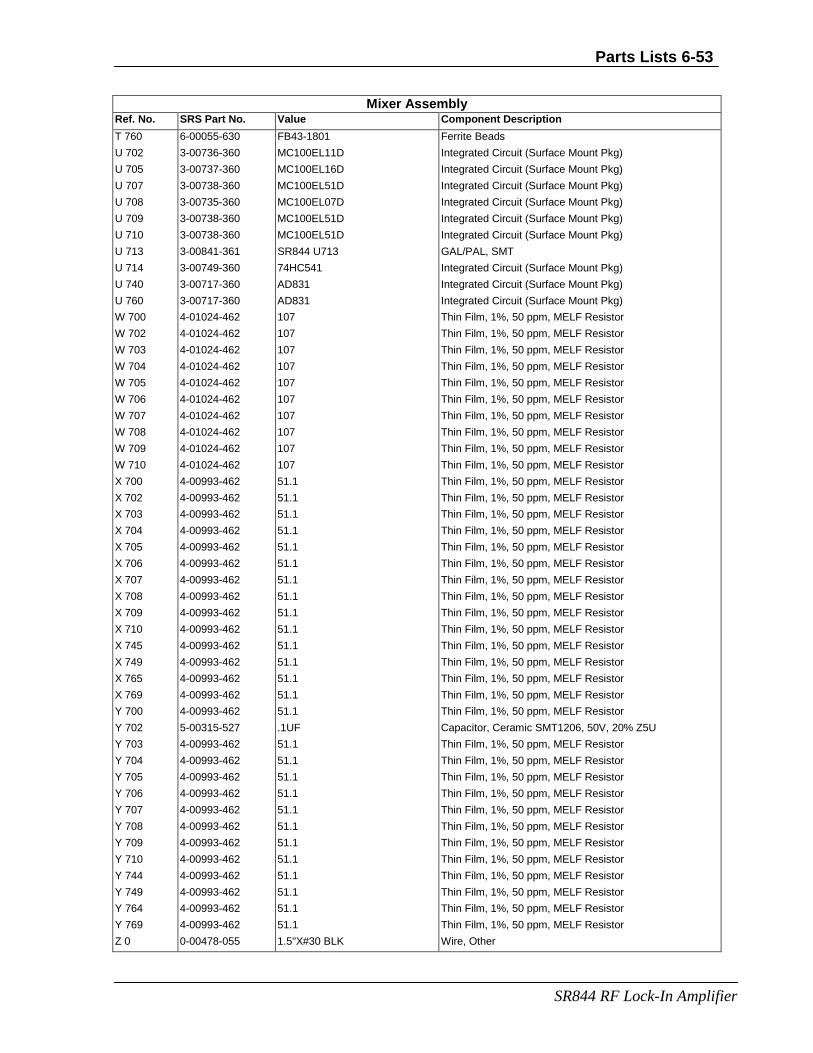
Parts Lists 6-53
SR844 RF Lock-In Amplifier
Mixer Assembly Ref. No. SRS Part No. Value Component Description
T 760 6-00055-630 FB43-1801 Ferrite Beads
U 702 3-00736-360 MC100EL11D Integrated Circuit (Surface Mount Pkg)
U 705 3-00737-360 MC100EL16D Integrated Circuit (Surface Mount Pkg)
U 707 3-00738-360 MC100EL51D Integrated Circuit (Surface Mount Pkg)
U 708 3-00735-360 MC100EL07D Integrated Circuit (Surface Mount Pkg)
U 709 3-00738-360 MC100EL51D Integrated Circuit (Surface Mount Pkg)
U 710 3-00738-360 MC100EL51D Integrated Circuit (Surface Mount Pkg)
U 713 3-00841-361 SR844 U713 GAL/PAL, SMT
U 714 3-00749-360 74HC541 Integrated Circuit (Surface Mount Pkg)
U 740 3-00717-360 AD831 Integrated Circuit (Surface Mount Pkg)
U 760 3-00717-360 AD831 Integrated Circuit (Surface Mount Pkg)
W 700 4-01024-462 107 Thin Film, 1%, 50 ppm, MELF Resistor
W 702 4-01024-462 107 Thin Film, 1%, 50 ppm, MELF Resistor
W 703 4-01024-462 107 Thin Film, 1%, 50 ppm, MELF Resistor
W 704 4-01024-462 107 Thin Film, 1%, 50 ppm, MELF Resistor
W 705 4-01024-462 107 Thin Film, 1%, 50 ppm, MELF Resistor
W 706 4-01024-462 107 Thin Film, 1%, 50 ppm, MELF Resistor
W 707 4-01024-462 107 Thin Film, 1%, 50 ppm, MELF Resistor
W 708 4-01024-462 107 Thin Film, 1%, 50 ppm, MELF Resistor
W 709 4-01024-462 107 Thin Film, 1%, 50 ppm, MELF Resistor
W 710 4-01024-462 107 Thin Film, 1%, 50 ppm, MELF Resistor
X 700 4-00993-462 51.1 Thin Film, 1%, 50 ppm, MELF Resistor
X 702 4-00993-462 51.1 Thin Film, 1%, 50 ppm, MELF Resistor
X 703 4-00993-462 51.1 Thin Film, 1%, 50 ppm, MELF Resistor
X 704 4-00993-462 51.1 Thin Film, 1%, 50 ppm, MELF Resistor
X 705 4-00993-462 51.1 Thin Film, 1%, 50 ppm, MELF Resistor
X 706 4-00993-462 51.1 Thin Film, 1%, 50 ppm, MELF Resistor
X 707 4-00993-462 51.1 Thin Film, 1%, 50 ppm, MELF Resistor
X 708 4-00993-462 51.1 Thin Film, 1%, 50 ppm, MELF Resistor
X 709 4-00993-462 51.1 Thin Film, 1%, 50 ppm, MELF Resistor
X 710 4-00993-462 51.1 Thin Film, 1%, 50 ppm, MELF Resistor
X 745 4-00993-462 51.1 Thin Film, 1%, 50 ppm, MELF Resistor
X 749 4-00993-462 51.1 Thin Film, 1%, 50 ppm, MELF Resistor
X 765 4-00993-462 51.1 Thin Film, 1%, 50 ppm, MELF Resistor
X 769 4-00993-462 51.1 Thin Film, 1%, 50 ppm, MELF Resistor
Y 700 4-00993-462 51.1 Thin Film, 1%, 50 ppm, MELF Resistor
Y 702 5-00315-527 .1UF Capacitor, Ceramic SMT1206, 50V, 20% Z5U
Y 703 4-00993-462 51.1 Thin Film, 1%, 50 ppm, MELF Resistor
Y 704 4-00993-462 51.1 Thin Film, 1%, 50 ppm, MELF Resistor
Y 705 4-00993-462 51.1 Thin Film, 1%, 50 ppm, MELF Resistor
Y 706 4-00993-462 51.1 Thin Film, 1%, 50 ppm, MELF Resistor
Y 707 4-00993-462 51.1 Thin Film, 1%, 50 ppm, MELF Resistor
Y 708 4-00993-462 51.1 Thin Film, 1%, 50 ppm, MELF Resistor
Y 709 4-00993-462 51.1 Thin Film, 1%, 50 ppm, MELF Resistor
Y 710 4-00993-462 51.1 Thin Film, 1%, 50 ppm, MELF Resistor
Y 744 4-00993-462 51.1 Thin Film, 1%, 50 ppm, MELF Resistor
Y 749 4-00993-462 51.1 Thin Film, 1%, 50 ppm, MELF Resistor
Y 764 4-00993-462 51.1 Thin Film, 1%, 50 ppm, MELF Resistor
Y 769 4-00993-462 51.1 Thin Film, 1%, 50 ppm, MELF Resistor
Z 0 0-00478-055 1.5"X#30 BLK Wire, Other

Parts Lists
SR844 RF Lock-In Amplifier
6-54
Mixer Assembly Ref. No. SRS Part No. Value Component Description
Z 0 0-00479-055 1.5"X#30 ORA Wire, Other
Z 0 1-00143-101 TEST JACK Vertical Test Jack
Z 700 5-00315-527 .1UF Capacitor, Ceramic SMT1206, 50V, 20% Z5U
Z 702 4-00993-462 51.1 Thin Film, 1%, 50 ppm, MELF Resistor
Z 703 5-00315-527 .1UF Capacitor, Ceramic SMT1206, 50V, 20% Z5U
Z 704 5-00315-527 .1UF Capacitor, Ceramic SMT1206, 50V, 20% Z5U
Z 705 5-00315-527 .1UF Capacitor, Ceramic SMT1206, 50V, 20% Z5U
Z 706 5-00315-527 .1UF Capacitor, Ceramic SMT1206, 50V, 20% Z5U
Z 707 5-00315-527 .1UF Capacitor, Ceramic SMT1206, 50V, 20% Z5U
Z 708 5-00315-527 .1UF Capacitor, Ceramic SMT1206, 50V, 20% Z5U
Z 709 5-00315-527 .1UF Capacitor, Ceramic SMT1206, 50V, 20% Z5U
Z 710 5-00315-527 .1UF Capacitor, Ceramic SMT1206, 50V, 20% Z5U
Z 713 5-00315-527 .1UF Capacitor, Ceramic SMT1206, 50V, 20% Z5U
Z 721 5-00315-527 .1UF Capacitor, Ceramic SMT1206, 50V, 20% Z5U
Z 722 5-00315-527 .1UF Capacitor, Ceramic SMT1206, 50V, 20% Z5U
Z 723 5-00315-527 .1UF Capacitor, Ceramic SMT1206, 50V, 20% Z5U
Z 725 5-00315-527 .1UF Capacitor, Ceramic SMT1206, 50V, 20% Z5U
Z 727 5-00315-527 .1UF Capacitor, Ceramic SMT1206, 50V, 20% Z5U
Z 728 5-00315-527 .1UF Capacitor, Ceramic SMT1206, 50V, 20% Z5U
Z 729 5-00315-527 .1UF Capacitor, Ceramic SMT1206, 50V, 20% Z5U
Z 730 5-00315-527 .1UF Capacitor, Ceramic SMT1206, 50V, 20% Z5U
Z 740 5-00315-527 .1UF Capacitor, Ceramic SMT1206, 50V, 20% Z5U
Z 741 5-00315-527 .1UF Capacitor, Ceramic SMT1206, 50V, 20% Z5U
Z 742 5-00315-527 .1UF Capacitor, Ceramic SMT1206, 50V, 20% Z5U
Z 743 5-00315-527 .1UF Capacitor, Ceramic SMT1206, 50V, 20% Z5U
Z 744 5-00315-527 .1UF Capacitor, Ceramic SMT1206, 50V, 20% Z5U
Z 745 5-00315-527 .1UF Capacitor, Ceramic SMT1206, 50V, 20% Z5U
Z 747 5-00315-527 .1UF Capacitor, Ceramic SMT1206, 50V, 20% Z5U
Z 748 5-00315-527 .1UF Capacitor, Ceramic SMT1206, 50V, 20% Z5U
Z 749 5-00315-527 .1UF Capacitor, Ceramic SMT1206, 50V, 20% Z5U
Z 760 5-00315-527 .1UF Capacitor, Ceramic SMT1206, 50V, 20% Z5U
Z 761 5-00315-527 .1UF Capacitor, Ceramic SMT1206, 50V, 20% Z5U
Z 762 5-00315-527 .1UF Capacitor, Ceramic SMT1206, 50V, 20% Z5U
Z 763 5-00315-527 .1UF Capacitor, Ceramic SMT1206, 50V, 20% Z5U
Z 764 5-00315-527 .1UF Capacitor, Ceramic SMT1206, 50V, 20% Z5U
Z 765 5-00315-527 .1UF Capacitor, Ceramic SMT1206, 50V, 20% Z5U
Z 767 5-00315-527 .1UF Capacitor, Ceramic SMT1206, 50V, 20% Z5U
Z 768 5-00315-527 .1UF Capacitor, Ceramic SMT1206, 50V, 20% Z5U
Z 769 5-00315-527 .1UF Capacitor, Ceramic SMT1206, 50V, 20% Z5U

Parts Lists 6-55
SR844 RF Lock-In Amplifier
IF Amplifier (84IFN) Board Parts List
If Amplifier Assembly Ref. No. SRS Part No. Value Component Description
C 400 5-00148-545 1000P Capacitor, Monolythic Ceramic, COG, 1%
C 401 5-00148-545 1000P Capacitor, Monolythic Ceramic, COG, 1%
C 402 5-00367-552 22P Capacitor, Chip (SMT1206), 50V, 5%, NPO
C 403 5-00367-552 22P Capacitor, Chip (SMT1206), 50V, 5%, NPO
C 404 5-00374-552 82P Capacitor, Chip (SMT1206), 50V, 5%, NPO
C 405 5-00374-552 82P Capacitor, Chip (SMT1206), 50V, 5%, NPO
C 406 5-00366-552 18P Capacitor, Chip (SMT1206), 50V, 5%, NPO
C 407 5-00375-552 100P Capacitor, Chip (SMT1206), 50V, 5%, NPO
C 408 5-00375-552 100P Capacitor, Chip (SMT1206), 50V, 5%, NPO
C 409 5-00379-552 220P Capacitor, Chip (SMT1206), 50V, 5%, NPO
C 410 5-00057-512 .22U Cap, Stacked Metal Film 50V 5% -40/+85c
C 411 5-00366-552 18P Capacitor, Chip (SMT1206), 50V, 5%, NPO
C 412 5-00379-552 220P Capacitor, Chip (SMT1206), 50V, 5%, NPO
C 413 5-00469-512 .56U Cap, Stacked Metal Film 50V 5% -40/+85c
C 414 5-00366-552 18P Capacitor, Chip (SMT1206), 50V, 5%, NPO
C 415 5-00379-552 220P Capacitor, Chip (SMT1206), 50V, 5%, NPO
C 416 5-00149-545 .01U Capacitor, Monolythic Ceramic, COG, 1%
C 417 5-00149-545 .01U Capacitor, Monolythic Ceramic, COG, 1%
C 418 5-00149-545 .01U Capacitor, Monolythic Ceramic, COG, 1%
C 419 5-00149-545 .01U Capacitor, Monolythic Ceramic, COG, 1%
C 420 5-00149-545 .01U Capacitor, Monolythic Ceramic, COG, 1%
C 421 5-00149-545 .01U Capacitor, Monolythic Ceramic, COG, 1%
C 422 5-00149-545 .01U Capacitor, Monolythic Ceramic, COG, 1%
C 423 5-00389-552 1500P Capacitor, Chip (SMT1206), 50V, 5%, NPO
C 470 5-00382-552 390P Capacitor, Chip (SMT1206), 50V, 5%, NPO
C 471 5-00382-552 390P Capacitor, Chip (SMT1206), 50V, 5%, NPO
C 472 5-00298-568 .01U Cap, Ceramic 50V SMT (1206) +/-10% X7R
C 473 5-00382-552 390P Capacitor, Chip (SMT1206), 50V, 5%, NPO
C 474 5-00382-552 390P Capacitor, Chip (SMT1206), 50V, 5%, NPO
C 475 5-00468-512 .056U Cap, Stacked Metal Film 50V 5% -40/+85c
C 476 5-00468-512 .056U Cap, Stacked Metal Film 50V 5% -40/+85c
C 477 5-00468-512 .056U Cap, Stacked Metal Film 50V 5% -40/+85c
C 478 5-00468-512 .056U Cap, Stacked Metal Film 50V 5% -40/+85c
C 479 5-00468-512 .056U Cap, Stacked Metal Film 50V 5% -40/+85c
C 480 5-00298-568 .01U Cap, Ceramic 50V SMT (1206) +/-10% X7R
C 481 5-00382-552 390P Capacitor, Chip (SMT1206), 50V, 5%, NPO
C 482 5-00385-552 680P Capacitor, Chip (SMT1206), 50V, 5%, NPO
C 483 5-00375-552 100P Capacitor, Chip (SMT1206), 50V, 5%, NPO
C 484 5-00298-568 .01U Cap, Ceramic 50V SMT (1206) +/-10% X7R
C 485 5-00298-568 .01U Cap, Ceramic 50V SMT (1206) +/-10% X7R
C 486 5-00298-568 .01U Cap, Ceramic 50V SMT (1206) +/-10% X7R
C 487 5-00298-568 .01U Cap, Ceramic 50V SMT (1206) +/-10% X7R
C 488 5-00382-552 390P Capacitor, Chip (SMT1206), 50V, 5%, NPO
C 500 5-00148-545 1000P Capacitor, Monolythic Ceramic, COG, 1%
C 501 5-00148-545 1000P Capacitor, Monolythic Ceramic, COG, 1%
C 502 5-00367-552 22P Capacitor, Chip (SMT1206), 50V, 5%, NPO
C 503 5-00367-552 22P Capacitor, Chip (SMT1206), 50V, 5%, NPO

Parts Lists
SR844 RF Lock-In Amplifier
6-56
If Amplifier Assembly Ref. No. SRS Part No. Value Component Description
C 504 5-00374-552 82P Capacitor, Chip (SMT1206), 50V, 5%, NPO
C 505 5-00374-552 82P Capacitor, Chip (SMT1206), 50V, 5%, NPO
C 506 5-00366-552 18P Capacitor, Chip (SMT1206), 50V, 5%, NPO
C 507 5-00375-552 100P Capacitor, Chip (SMT1206), 50V, 5%, NPO
C 508 5-00375-552 100P Capacitor, Chip (SMT1206), 50V, 5%, NPO
C 509 5-00379-552 220P Capacitor, Chip (SMT1206), 50V, 5%, NPO
C 510 5-00057-512 .22U Cap, Stacked Metal Film 50V 5% -40/+85c
C 511 5-00366-552 18P Capacitor, Chip (SMT1206), 50V, 5%, NPO
C 512 5-00379-552 220P Capacitor, Chip (SMT1206), 50V, 5%, NPO
C 513 5-00469-512 .56U Cap, Stacked Metal Film 50V 5% -40/+85c
C 514 5-00366-552 18P Capacitor, Chip (SMT1206), 50V, 5%, NPO
C 515 5-00379-552 220P Capacitor, Chip (SMT1206), 50V, 5%, NPO
C 516 5-00149-545 .01U Capacitor, Monolythic Ceramic, COG, 1%
C 517 5-00149-545 .01U Capacitor, Monolythic Ceramic, COG, 1%
C 518 5-00149-545 .01U Capacitor, Monolythic Ceramic, COG, 1%
C 519 5-00149-545 .01U Capacitor, Monolythic Ceramic, COG, 1%
C 520 5-00149-545 .01U Capacitor, Monolythic Ceramic, COG, 1%
C 521 5-00149-545 .01U Capacitor, Monolythic Ceramic, COG, 1%
C 522 5-00149-545 .01U Capacitor, Monolythic Ceramic, COG, 1%
C 523 5-00389-552 1500P Capacitor, Chip (SMT1206), 50V, 5%, NPO
F 420 5-00318-569 2.2U/T35 Cap, Tantalum, SMT (all case sizes)
F 421 5-00318-569 2.2U/T35 Cap, Tantalum, SMT (all case sizes)
F 422 5-00318-569 2.2U/T35 Cap, Tantalum, SMT (all case sizes)
F 423 5-00318-569 2.2U/T35 Cap, Tantalum, SMT (all case sizes)
F 424 5-00318-569 2.2U/T35 Cap, Tantalum, SMT (all case sizes)
F 425 5-00318-569 2.2U/T35 Cap, Tantalum, SMT (all case sizes)
F 426 5-00318-569 2.2U/T35 Cap, Tantalum, SMT (all case sizes)
F 427 5-00318-569 2.2U/T35 Cap, Tantalum, SMT (all case sizes)
F 430 5-00318-569 2.2U/T35 Cap, Tantalum, SMT (all case sizes)
F 431 5-00318-569 2.2U/T35 Cap, Tantalum, SMT (all case sizes)
F 432 5-00318-569 2.2U/T35 Cap, Tantalum, SMT (all case sizes)
F 433 5-00318-569 2.2U/T35 Cap, Tantalum, SMT (all case sizes)
F 434 5-00318-569 2.2U/T35 Cap, Tantalum, SMT (all case sizes)
F 435 5-00318-569 2.2U/T35 Cap, Tantalum, SMT (all case sizes)
F 436 5-00318-569 2.2U/T35 Cap, Tantalum, SMT (all case sizes)
F 437 5-00318-569 2.2U/T35 Cap, Tantalum, SMT (all case sizes)
F 478 5-00471-569 10U/T16 Cap, Tantalum, SMT (all case sizes)
F 479 5-00471-569 10U/T16 Cap, Tantalum, SMT (all case sizes)
F 480 5-00318-569 2.2U/T35 Cap, Tantalum, SMT (all case sizes)
F 481 5-00318-569 2.2U/T35 Cap, Tantalum, SMT (all case sizes)
F 482 5-00318-569 2.2U/T35 Cap, Tantalum, SMT (all case sizes)
F 483 5-00318-569 2.2U/T35 Cap, Tantalum, SMT (all case sizes)
F 484 5-00318-569 2.2U/T35 Cap, Tantalum, SMT (all case sizes)
F 485 5-00318-569 2.2U/T35 Cap, Tantalum, SMT (all case sizes)
F 486 5-00318-569 2.2U/T35 Cap, Tantalum, SMT (all case sizes)
F 487 5-00318-569 2.2U/T35 Cap, Tantalum, SMT (all case sizes)
F 488 5-00471-569 10U/T16 Cap, Tantalum, SMT (all case sizes)
F 489 5-00318-569 2.2U/T35 Cap, Tantalum, SMT (all case sizes)
F 490 5-00318-569 2.2U/T35 Cap, Tantalum, SMT (all case sizes)
F 491 5-00318-569 2.2U/T35 Cap, Tantalum, SMT (all case sizes)

Parts Lists 6-57
SR844 RF Lock-In Amplifier
If Amplifier Assembly Ref. No. SRS Part No. Value Component Description
F 492 5-00318-569 2.2U/T35 Cap, Tantalum, SMT (all case sizes)
F 493 5-00318-569 2.2U/T35 Cap, Tantalum, SMT (all case sizes)
F 494 5-00318-569 2.2U/T35 Cap, Tantalum, SMT (all case sizes)
F 495 5-00318-569 2.2U/T35 Cap, Tantalum, SMT (all case sizes)
F 496 5-00318-569 2.2U/T35 Cap, Tantalum, SMT (all case sizes)
F 497 5-00318-569 2.2U/T35 Cap, Tantalum, SMT (all case sizes)
F 498 5-00471-569 10U/T16 Cap, Tantalum, SMT (all case sizes)
F 499 5-00318-569 2.2U/T35 Cap, Tantalum, SMT (all case sizes)
F 520 5-00318-569 2.2U/T35 Cap, Tantalum, SMT (all case sizes)
F 521 5-00318-569 2.2U/T35 Cap, Tantalum, SMT (all case sizes)
F 522 5-00318-569 2.2U/T35 Cap, Tantalum, SMT (all case sizes)
F 524 5-00318-569 2.2U/T35 Cap, Tantalum, SMT (all case sizes)
F 525 5-00318-569 2.2U/T35 Cap, Tantalum, SMT (all case sizes)
F 526 5-00318-569 2.2U/T35 Cap, Tantalum, SMT (all case sizes)
F 527 5-00318-569 2.2U/T35 Cap, Tantalum, SMT (all case sizes)
F 530 5-00318-569 2.2U/T35 Cap, Tantalum, SMT (all case sizes)
F 531 5-00318-569 2.2U/T35 Cap, Tantalum, SMT (all case sizes)
F 532 5-00318-569 2.2U/T35 Cap, Tantalum, SMT (all case sizes)
F 534 5-00318-569 2.2U/T35 Cap, Tantalum, SMT (all case sizes)
F 535 5-00318-569 2.2U/T35 Cap, Tantalum, SMT (all case sizes)
F 536 5-00318-569 2.2U/T35 Cap, Tantalum, SMT (all case sizes)
F 537 5-00318-569 2.2U/T35 Cap, Tantalum, SMT (all case sizes)
J 15 1-00301-131 4 PIN DIF CES Connector, Female
J 40 1-00290-130 8 PIN DI TSW 07 Connector, Male
J 41 1-00290-130 8 PIN DI TSW 07 Connector, Male
J 42 1-00281-130 10 PIN DI Connector, Male
J 43 1-00289-130 6 PIN DI TSW 07 Connector, Male
J 44 1-00288-130 4 PIN DI TSW 07 Connector, Male
J 45 1-00288-130 4 PIN DI TSW 07 Connector, Male
L 400 6-00236-631 FR47 Ferrite bead, SMT
L 401 6-00236-631 FR47 Ferrite bead, SMT
N 400 4-00911-463 4.7KX4D Resistor network, SMT, Leadless
N 500 4-00911-463 4.7KX4D Resistor network, SMT, Leadless
N 591 4-00911-463 4.7KX4D Resistor network, SMT, Leadless
PC0 7-00586-701 SR844 IF&NOISE Printed Circuit Board
R 400 4-01001-462 61.9 Thin Film, 1%, 50 ppm, MELF Resistor
R 401 4-01001-462 61.9 Thin Film, 1%, 50 ppm, MELF Resistor
R 402 4-01059-462 249 Thin Film, 1%, 50 ppm, MELF Resistor
R 403 4-01059-462 249 Thin Film, 1%, 50 ppm, MELF Resistor
R 404 4-01175-462 4.02K Thin Film, 1%, 50 ppm, MELF Resistor
R 405 4-01150-462 2.21K Thin Film, 1%, 50 ppm, MELF Resistor
R 406 4-01305-462 90.9K Thin Film, 1%, 50 ppm, MELF Resistor
R 407 4-01181-462 4.64K Thin Film, 1%, 50 ppm, MELF Resistor
R 408 4-01181-462 4.64K Thin Film, 1%, 50 ppm, MELF Resistor
R 409 4-01053-462 215 Thin Film, 1%, 50 ppm, MELF Resistor
R 410 4-01146-462 2.00K Thin Film, 1%, 50 ppm, MELF Resistor
R 411 4-01181-462 4.64K Thin Film, 1%, 50 ppm, MELF Resistor
R 412 4-01053-462 215 Thin Film, 1%, 50 ppm, MELF Resistor
R 413 4-01009-462 75 Thin Film, 1%, 50 ppm, MELF Resistor
R 414 4-01153-462 2.37K Thin Film, 1%, 50 ppm, MELF Resistor

Parts Lists
SR844 RF Lock-In Amplifier
6-58
If Amplifier Assembly Ref. No. SRS Part No. Value Component Description
R 415 4-01213-462 10.0K Thin Film, 1%, 50 ppm, MELF Resistor
R 416 4-01167-462 3.32K Thin Film, 1%, 50 ppm, MELF Resistor
R 417 4-01175-462 4.02K Thin Film, 1%, 50 ppm, MELF Resistor
R 418 4-01020-462 97.6 Thin Film, 1%, 50 ppm, MELF Resistor
R 419 4-01150-462 2.21K Thin Film, 1%, 50 ppm, MELF Resistor
R 420 4-01146-462 2.00K Thin Film, 1%, 50 ppm, MELF Resistor
R 421 4-01181-462 4.64K Thin Film, 1%, 50 ppm, MELF Resistor
R 422 4-01175-462 4.02K Thin Film, 1%, 50 ppm, MELF Resistor
R 423 4-01084-462 453 Thin Film, 1%, 50 ppm, MELF Resistor
R 424 4-00960-462 23.2 Thin Film, 1%, 50 ppm, MELF Resistor
R 425 4-01175-462 4.02K Thin Film, 1%, 50 ppm, MELF Resistor
R 426 4-01181-462 4.64K Thin Film, 1%, 50 ppm, MELF Resistor
R 427 4-01150-462 2.21K Thin Film, 1%, 50 ppm, MELF Resistor
R 428 4-01146-462 2.00K Thin Film, 1%, 50 ppm, MELF Resistor
R 429 4-01181-462 4.64K Thin Film, 1%, 50 ppm, MELF Resistor
R 430 4-01175-462 4.02K Thin Film, 1%, 50 ppm, MELF Resistor
R 431 4-01084-462 453 Thin Film, 1%, 50 ppm, MELF Resistor
R 432 4-00960-462 23.2 Thin Film, 1%, 50 ppm, MELF Resistor
R 433 4-01175-462 4.02K Thin Film, 1%, 50 ppm, MELF Resistor
R 434 4-01181-462 4.64K Thin Film, 1%, 50 ppm, MELF Resistor
R 435 4-01305-462 90.9K Thin Film, 1%, 50 ppm, MELF Resistor
R 436 4-01120-462 1.07K Thin Film, 1%, 50 ppm, MELF Resistor
R 437 4-01053-462 215 Thin Film, 1%, 50 ppm, MELF Resistor
R 438 4-01059-462 249 Thin Film, 1%, 50 ppm, MELF Resistor
R 439 4-00993-462 51.1 Thin Film, 1%, 50 ppm, MELF Resistor
R 440 4-01133-462 1.47K Thin Film, 1%, 50 ppm, MELF Resistor
R 441 4-01461-461 180 Thick Film, 5%, 200 ppm, Chip Resistor
R 442 4-01129-462 1.33K Thin Film, 1%, 50 ppm, MELF Resistor
R 443 4-01133-462 1.47K Thin Film, 1%, 50 ppm, MELF Resistor
R 444 4-01124-462 1.18K Thin Film, 1%, 50 ppm, MELF Resistor
R 445 4-01053-462 215 Thin Film, 1%, 50 ppm, MELF Resistor
R 446 4-00942-462 15 Thin Film, 1%, 50 ppm, MELF Resistor
R 447 4-01053-462 215 Thin Film, 1%, 50 ppm, MELF Resistor
R 448 4-01124-462 1.18K Thin Film, 1%, 50 ppm, MELF Resistor
R 449 4-01124-462 1.18K Thin Film, 1%, 50 ppm, MELF Resistor
R 450 4-01124-462 1.18K Thin Film, 1%, 50 ppm, MELF Resistor
R 451 4-01124-462 1.18K Thin Film, 1%, 50 ppm, MELF Resistor
R 452 4-01053-462 215 Thin Film, 1%, 50 ppm, MELF Resistor
R 453 4-01117-462 1.00K Thin Film, 1%, 50 ppm, MELF Resistor
R 454 4-01117-462 1.00K Thin Film, 1%, 50 ppm, MELF Resistor
R 455 4-00960-462 23.2 Thin Film, 1%, 50 ppm, MELF Resistor
R 456 4-01124-462 1.18K Thin Film, 1%, 50 ppm, MELF Resistor
R 457 4-00942-462 15 Thin Film, 1%, 50 ppm, MELF Resistor
R 458 4-01070-462 324 Thin Film, 1%, 50 ppm, MELF Resistor
R 459 4-01471-461 470 Thick Film, 5%, 200 ppm, Chip Resistor
R 460 4-01471-461 470 Thick Film, 5%, 200 ppm, Chip Resistor
R 470 4-01305-462 90.9K Thin Film, 1%, 50 ppm, MELF Resistor
R 471 4-01305-462 90.9K Thin Film, 1%, 50 ppm, MELF Resistor
R 472 4-01305-462 90.9K Thin Film, 1%, 50 ppm, MELF Resistor
R 473 4-01305-462 90.9K Thin Film, 1%, 50 ppm, MELF Resistor

Parts Lists 6-59
SR844 RF Lock-In Amplifier
If Amplifier Assembly Ref. No. SRS Part No. Value Component Description
R 474 4-01070-462 324 Thin Film, 1%, 50 ppm, MELF Resistor
R 475 4-01305-462 90.9K Thin Film, 1%, 50 ppm, MELF Resistor
R 476 4-01305-462 90.9K Thin Film, 1%, 50 ppm, MELF Resistor
R 477 4-01305-462 90.9K Thin Film, 1%, 50 ppm, MELF Resistor
R 478 4-01305-462 90.9K Thin Film, 1%, 50 ppm, MELF Resistor
R 479 4-01305-462 90.9K Thin Film, 1%, 50 ppm, MELF Resistor
R 480 4-01129-462 1.33K Thin Film, 1%, 50 ppm, MELF Resistor
R 481 4-01305-462 90.9K Thin Film, 1%, 50 ppm, MELF Resistor
R 482 4-01037-462 147 Thin Film, 1%, 50 ppm, MELF Resistor
R 483 4-01175-462 4.02K Thin Film, 1%, 50 ppm, MELF Resistor
R 484 4-01037-462 147 Thin Film, 1%, 50 ppm, MELF Resistor
R 485 4-00960-462 23.2 Thin Film, 1%, 50 ppm, MELF Resistor
R 486 4-01175-462 4.02K Thin Film, 1%, 50 ppm, MELF Resistor
R 487 4-01133-462 1.47K Thin Film, 1%, 50 ppm, MELF Resistor
R 488 4-01129-462 1.33K Thin Film, 1%, 50 ppm, MELF Resistor
R 489 4-01150-462 2.21K Thin Film, 1%, 50 ppm, MELF Resistor
R 490 4-01153-462 2.37K Thin Film, 1%, 50 ppm, MELF Resistor
R 491 4-01117-462 1.00K Thin Film, 1%, 50 ppm, MELF Resistor
R 492 4-01129-462 1.33K Thin Film, 1%, 50 ppm, MELF Resistor
R 493 4-01162-462 2.94K Thin Film, 1%, 50 ppm, MELF Resistor
R 494 4-01133-462 1.47K Thin Film, 1%, 50 ppm, MELF Resistor
R 495 4-01129-462 1.33K Thin Film, 1%, 50 ppm, MELF Resistor
R 496 4-01141-462 1.78K Thin Film, 1%, 50 ppm, MELF Resistor
R 497 4-01175-462 4.02K Thin Film, 1%, 50 ppm, MELF Resistor
R 498 4-01305-462 90.9K Thin Film, 1%, 50 ppm, MELF Resistor
R 500 4-01001-462 61.9 Thin Film, 1%, 50 ppm, MELF Resistor
R 501 4-01001-462 61.9 Thin Film, 1%, 50 ppm, MELF Resistor
R 502 4-01059-462 249 Thin Film, 1%, 50 ppm, MELF Resistor
R 503 4-01059-462 249 Thin Film, 1%, 50 ppm, MELF Resistor
R 504 4-01175-462 4.02K Thin Film, 1%, 50 ppm, MELF Resistor
R 505 4-01150-462 2.21K Thin Film, 1%, 50 ppm, MELF Resistor
R 506 4-01305-462 90.9K Thin Film, 1%, 50 ppm, MELF Resistor
R 507 4-01181-462 4.64K Thin Film, 1%, 50 ppm, MELF Resistor
R 508 4-01181-462 4.64K Thin Film, 1%, 50 ppm, MELF Resistor
R 509 4-01053-462 215 Thin Film, 1%, 50 ppm, MELF Resistor
R 510 4-01146-462 2.00K Thin Film, 1%, 50 ppm, MELF Resistor
R 511 4-01181-462 4.64K Thin Film, 1%, 50 ppm, MELF Resistor
R 512 4-01053-462 215 Thin Film, 1%, 50 ppm, MELF Resistor
R 513 4-01009-462 75 Thin Film, 1%, 50 ppm, MELF Resistor
R 514 4-01153-462 2.37K Thin Film, 1%, 50 ppm, MELF Resistor
R 515 4-01213-462 10.0K Thin Film, 1%, 50 ppm, MELF Resistor
R 516 4-01167-462 3.32K Thin Film, 1%, 50 ppm, MELF Resistor
R 517 4-01175-462 4.02K Thin Film, 1%, 50 ppm, MELF Resistor
R 518 4-01020-462 97.6 Thin Film, 1%, 50 ppm, MELF Resistor
R 519 4-01150-462 2.21K Thin Film, 1%, 50 ppm, MELF Resistor
R 520 4-01146-462 2.00K Thin Film, 1%, 50 ppm, MELF Resistor
R 521 4-01181-462 4.64K Thin Film, 1%, 50 ppm, MELF Resistor
R 522 4-01175-462 4.02K Thin Film, 1%, 50 ppm, MELF Resistor
R 523 4-01084-462 453 Thin Film, 1%, 50 ppm, MELF Resistor
R 524 4-00960-462 23.2 Thin Film, 1%, 50 ppm, MELF Resistor

Parts Lists
SR844 RF Lock-In Amplifier
6-60
If Amplifier Assembly Ref. No. SRS Part No. Value Component Description
R 525 4-01175-462 4.02K Thin Film, 1%, 50 ppm, MELF Resistor
R 526 4-01181-462 4.64K Thin Film, 1%, 50 ppm, MELF Resistor
R 527 4-01150-462 2.21K Thin Film, 1%, 50 ppm, MELF Resistor
R 528 4-01146-462 2.00K Thin Film, 1%, 50 ppm, MELF Resistor
R 529 4-01181-462 4.64K Thin Film, 1%, 50 ppm, MELF Resistor
R 530 4-01175-462 4.02K Thin Film, 1%, 50 ppm, MELF Resistor
R 531 4-01084-462 453 Thin Film, 1%, 50 ppm, MELF Resistor
R 532 4-00960-462 23.2 Thin Film, 1%, 50 ppm, MELF Resistor
R 533 4-01175-462 4.02K Thin Film, 1%, 50 ppm, MELF Resistor
R 534 4-01181-462 4.64K Thin Film, 1%, 50 ppm, MELF Resistor
R 535 4-01305-462 90.9K Thin Film, 1%, 50 ppm, MELF Resistor
R 536 4-01120-462 1.07K Thin Film, 1%, 50 ppm, MELF Resistor
R 537 4-01053-462 215 Thin Film, 1%, 50 ppm, MELF Resistor
R 538 4-01059-462 249 Thin Film, 1%, 50 ppm, MELF Resistor
R 539 4-00993-462 51.1 Thin Film, 1%, 50 ppm, MELF Resistor
R 540 4-01133-462 1.47K Thin Film, 1%, 50 ppm, MELF Resistor
R 541 4-01461-461 180 Thick Film, 5%, 200 ppm, Chip Resistor
R 542 4-01129-462 1.33K Thin Film, 1%, 50 ppm, MELF Resistor
R 543 4-01133-462 1.47K Thin Film, 1%, 50 ppm, MELF Resistor
R 544 4-01124-462 1.18K Thin Film, 1%, 50 ppm, MELF Resistor
R 545 4-01053-462 215 Thin Film, 1%, 50 ppm, MELF Resistor
R 546 4-00942-462 15 Thin Film, 1%, 50 ppm, MELF Resistor
R 547 4-01053-462 215 Thin Film, 1%, 50 ppm, MELF Resistor
R 548 4-01124-462 1.18K Thin Film, 1%, 50 ppm, MELF Resistor
R 549 4-01124-462 1.18K Thin Film, 1%, 50 ppm, MELF Resistor
R 550 4-01124-462 1.18K Thin Film, 1%, 50 ppm, MELF Resistor
R 551 4-01124-462 1.18K Thin Film, 1%, 50 ppm, MELF Resistor
R 552 4-01053-462 215 Thin Film, 1%, 50 ppm, MELF Resistor
R 553 4-01117-462 1.00K Thin Film, 1%, 50 ppm, MELF Resistor
R 554 4-01117-462 1.00K Thin Film, 1%, 50 ppm, MELF Resistor
R 555 4-00960-462 23.2 Thin Film, 1%, 50 ppm, MELF Resistor
R 556 4-01124-462 1.18K Thin Film, 1%, 50 ppm, MELF Resistor
R 557 4-00942-462 15 Thin Film, 1%, 50 ppm, MELF Resistor
R 558 4-01070-462 324 Thin Film, 1%, 50 ppm, MELF Resistor
R 570 4-01153-462 2.37K Thin Film, 1%, 50 ppm, MELF Resistor
R 571 4-01153-462 2.37K Thin Film, 1%, 50 ppm, MELF Resistor
R 572 4-01124-462 1.18K Thin Film, 1%, 50 ppm, MELF Resistor
R 573 4-01181-462 4.64K Thin Film, 1%, 50 ppm, MELF Resistor
R 574 4-01150-462 2.21K Thin Film, 1%, 50 ppm, MELF Resistor
R 575 4-01505-461 12K Thick Film, 5%, 200 ppm, Chip Resistor
R 576 4-01117-462 1.00K Thin Film, 1%, 50 ppm, MELF Resistor
R 577 4-01213-462 10.0K Thin Film, 1%, 50 ppm, MELF Resistor
R 578 4-01213-462 10.0K Thin Film, 1%, 50 ppm, MELF Resistor
R 579 4-01505-461 12K Thick Film, 5%, 200 ppm, Chip Resistor
R 580 4-01505-461 12K Thick Film, 5%, 200 ppm, Chip Resistor
R 581 4-01477-461 820 Thick Film, 5%, 200 ppm, Chip Resistor
R 582 4-01477-461 820 Thick Film, 5%, 200 ppm, Chip Resistor
R 583 4-01117-462 1.00K Thin Film, 1%, 50 ppm, MELF Resistor
R 584 4-01117-462 1.00K Thin Film, 1%, 50 ppm, MELF Resistor
R 585 4-00993-462 51.1 Thin Film, 1%, 50 ppm, MELF Resistor

Parts Lists 6-61
SR844 RF Lock-In Amplifier
If Amplifier Assembly Ref. No. SRS Part No. Value Component Description
R 586 4-00993-462 51.1 Thin Film, 1%, 50 ppm, MELF Resistor
R 587 4-01477-461 820 Thick Film, 5%, 200 ppm, Chip Resistor
R 588 4-01477-461 820 Thick Film, 5%, 200 ppm, Chip Resistor
R 589 4-01455-461 100 Thick Film, 5%, 200 ppm, Chip Resistor
R 590 4-01455-461 100 Thick Film, 5%, 200 ppm, Chip Resistor
R 591 4-01505-461 12K Thick Film, 5%, 200 ppm, Chip Resistor
R 592 4-01167-462 3.32K Thin Film, 1%, 50 ppm, MELF Resistor
U 400 3-00731-360 5534 Integrated Circuit (Surface Mount Pkg)
U 401 3-00731-360 5534 Integrated Circuit (Surface Mount Pkg)
U 402 3-00752-360 4052 Integrated Circuit (Surface Mount Pkg)
U 403 3-00730-360 5532 Integrated Circuit (Surface Mount Pkg)
U 404 3-00753-360 4053 Integrated Circuit (Surface Mount Pkg)
U 405 3-00643-360 DG211BDY Integrated Circuit (Surface Mount Pkg)
U 406 3-00818-360 LM833 Integrated Circuit (Surface Mount Pkg)
U 407 3-00818-360 LM833 Integrated Circuit (Surface Mount Pkg)
U 408 3-00818-360 LM833 Integrated Circuit (Surface Mount Pkg)
U 409 3-00753-360 4053 Integrated Circuit (Surface Mount Pkg)
U 410 3-00730-360 5532 Integrated Circuit (Surface Mount Pkg)
U 470 3-00729-360 LM741C Integrated Circuit (Surface Mount Pkg)
U 471 3-00729-360 LM741C Integrated Circuit (Surface Mount Pkg)
U 472 3-00724-360 LF353 Integrated Circuit (Surface Mount Pkg)
U 473 3-00724-360 LF353 Integrated Circuit (Surface Mount Pkg)
U 474 3-00726-360 LF412 Integrated Circuit (Surface Mount Pkg)
U 475 3-00724-360 LF353 Integrated Circuit (Surface Mount Pkg)
U 476 3-00753-360 4053 Integrated Circuit (Surface Mount Pkg)
U 477 3-00742-360 74HC74 Integrated Circuit (Surface Mount Pkg)
U 478 3-00757-360 PCM1750U Integrated Circuit (Surface Mount Pkg)
U 479 3-00724-360 LF353 Integrated Circuit (Surface Mount Pkg)
U 480 3-00727-360 LM339 Integrated Circuit (Surface Mount Pkg)
U 481 3-00709-360 78L05 Integrated Circuit (Surface Mount Pkg)
U 482 3-00712-360 79L05 Integrated Circuit (Surface Mount Pkg)
U 483 3-00709-360 78L05 Integrated Circuit (Surface Mount Pkg)
U 484 3-00712-360 79L05 Integrated Circuit (Surface Mount Pkg)
U 500 3-00731-360 5534 Integrated Circuit (Surface Mount Pkg)
U 501 3-00731-360 5534 Integrated Circuit (Surface Mount Pkg)
U 503 3-00730-360 5532 Integrated Circuit (Surface Mount Pkg)
U 504 3-00753-360 4053 Integrated Circuit (Surface Mount Pkg)
U 506 3-00818-360 LM833 Integrated Circuit (Surface Mount Pkg)
U 507 3-00818-360 LM833 Integrated Circuit (Surface Mount Pkg)
U 508 3-00818-360 LM833 Integrated Circuit (Surface Mount Pkg)
U 509 3-00753-360 4053 Integrated Circuit (Surface Mount Pkg)
U 510 3-00730-360 5532 Integrated Circuit (Surface Mount Pkg)
U 591 3-00728-360 LM393 Integrated Circuit (Surface Mount Pkg)
V 420 4-01461-461 180 Thick Film, 5%, 200 ppm, Chip Resistor
V 421 4-01461-461 180 Thick Film, 5%, 200 ppm, Chip Resistor
V 422 4-01461-461 180 Thick Film, 5%, 200 ppm, Chip Resistor
V 423 4-01461-461 180 Thick Film, 5%, 200 ppm, Chip Resistor
V 424 4-01461-461 180 Thick Film, 5%, 200 ppm, Chip Resistor
V 425 4-01461-461 180 Thick Film, 5%, 200 ppm, Chip Resistor
V 426 4-01461-461 180 Thick Film, 5%, 200 ppm, Chip Resistor

Parts Lists
SR844 RF Lock-In Amplifier
6-62
If Amplifier Assembly Ref. No. SRS Part No. Value Component Description
V 427 4-01461-461 180 Thick Film, 5%, 200 ppm, Chip Resistor
V 430 4-01461-461 180 Thick Film, 5%, 200 ppm, Chip Resistor
V 431 4-01461-461 180 Thick Film, 5%, 200 ppm, Chip Resistor
V 432 4-01461-461 180 Thick Film, 5%, 200 ppm, Chip Resistor
V 433 4-01461-461 180 Thick Film, 5%, 200 ppm, Chip Resistor
V 434 4-01461-461 180 Thick Film, 5%, 200 ppm, Chip Resistor
V 435 4-01461-461 180 Thick Film, 5%, 200 ppm, Chip Resistor
V 436 4-01461-461 180 Thick Film, 5%, 200 ppm, Chip Resistor
V 437 4-01461-461 180 Thick Film, 5%, 200 ppm, Chip Resistor
V 481 4-01461-461 180 Thick Film, 5%, 200 ppm, Chip Resistor
V 482 4-01461-461 180 Thick Film, 5%, 200 ppm, Chip Resistor
V 483 4-01461-461 180 Thick Film, 5%, 200 ppm, Chip Resistor
V 485 4-01461-461 180 Thick Film, 5%, 200 ppm, Chip Resistor
V 491 4-01461-461 180 Thick Film, 5%, 200 ppm, Chip Resistor
V 492 4-01461-461 180 Thick Film, 5%, 200 ppm, Chip Resistor
V 493 4-01461-461 180 Thick Film, 5%, 200 ppm, Chip Resistor
V 495 4-01461-461 180 Thick Film, 5%, 200 ppm, Chip Resistor
V 520 4-01461-461 180 Thick Film, 5%, 200 ppm, Chip Resistor
V 521 4-01461-461 180 Thick Film, 5%, 200 ppm, Chip Resistor
V 522 4-01461-461 180 Thick Film, 5%, 200 ppm, Chip Resistor
V 524 4-01461-461 180 Thick Film, 5%, 200 ppm, Chip Resistor
V 525 4-01461-461 180 Thick Film, 5%, 200 ppm, Chip Resistor
V 526 4-01461-461 180 Thick Film, 5%, 200 ppm, Chip Resistor
V 527 4-01461-461 180 Thick Film, 5%, 200 ppm, Chip Resistor
V 530 4-01461-461 180 Thick Film, 5%, 200 ppm, Chip Resistor
V 531 4-01461-461 180 Thick Film, 5%, 200 ppm, Chip Resistor
V 532 4-01461-461 180 Thick Film, 5%, 200 ppm, Chip Resistor
V 534 4-01461-461 180 Thick Film, 5%, 200 ppm, Chip Resistor
V 535 4-01461-461 180 Thick Film, 5%, 200 ppm, Chip Resistor
V 536 4-01461-461 180 Thick Film, 5%, 200 ppm, Chip Resistor
V 537 4-01461-461 180 Thick Film, 5%, 200 ppm, Chip Resistor
Z 0 1-00143-101 TEST JACK Vertical Test Jack
Z 400 5-00315-527 .1UF Capacitor, Ceramic SMT1206, 50V, 20% Z5U
Z 401 5-00315-527 .1UF Capacitor, Ceramic SMT1206, 50V, 20% Z5U
Z 402 5-00315-527 .1UF Capacitor, Ceramic SMT1206, 50V, 20% Z5U
Z 403 5-00315-527 .1UF Capacitor, Ceramic SMT1206, 50V, 20% Z5U
Z 404 5-00315-527 .1UF Capacitor, Ceramic SMT1206, 50V, 20% Z5U
Z 405 5-00315-527 .1UF Capacitor, Ceramic SMT1206, 50V, 20% Z5U
Z 406 5-00315-527 .1UF Capacitor, Ceramic SMT1206, 50V, 20% Z5U
Z 407 5-00315-527 .1UF Capacitor, Ceramic SMT1206, 50V, 20% Z5U
Z 408 5-00315-527 .1UF Capacitor, Ceramic SMT1206, 50V, 20% Z5U
Z 409 5-00315-527 .1UF Capacitor, Ceramic SMT1206, 50V, 20% Z5U
Z 410 5-00315-527 .1UF Capacitor, Ceramic SMT1206, 50V, 20% Z5U
Z 411 5-00315-527 .1UF Capacitor, Ceramic SMT1206, 50V, 20% Z5U
Z 412 5-00315-527 .1UF Capacitor, Ceramic SMT1206, 50V, 20% Z5U
Z 413 5-00315-527 .1UF Capacitor, Ceramic SMT1206, 50V, 20% Z5U
Z 414 5-00315-527 .1UF Capacitor, Ceramic SMT1206, 50V, 20% Z5U
Z 479 5-00315-527 .1UF Capacitor, Ceramic SMT1206, 50V, 20% Z5U
Z 480 5-00315-527 .1UF Capacitor, Ceramic SMT1206, 50V, 20% Z5U
Z 481 5-00315-527 .1UF Capacitor, Ceramic SMT1206, 50V, 20% Z5U

Parts Lists 6-63
SR844 RF Lock-In Amplifier
If Amplifier Assembly Ref. No. SRS Part No. Value Component Description
Z 482 5-00315-527 .1UF Capacitor, Ceramic SMT1206, 50V, 20% Z5U
Z 483 5-00315-527 .1UF Capacitor, Ceramic SMT1206, 50V, 20% Z5U
Z 484 5-00315-527 .1UF Capacitor, Ceramic SMT1206, 50V, 20% Z5U
Z 485 5-00315-527 .1UF Capacitor, Ceramic SMT1206, 50V, 20% Z5U
Z 486 5-00315-527 .1UF Capacitor, Ceramic SMT1206, 50V, 20% Z5U
Z 490 5-00315-527 .1UF Capacitor, Ceramic SMT1206, 50V, 20% Z5U
Z 491 5-00315-527 .1UF Capacitor, Ceramic SMT1206, 50V, 20% Z5U
Z 492 5-00315-527 .1UF Capacitor, Ceramic SMT1206, 50V, 20% Z5U
Z 493 5-00315-527 .1UF Capacitor, Ceramic SMT1206, 50V, 20% Z5U
Z 494 5-00315-527 .1UF Capacitor, Ceramic SMT1206, 50V, 20% Z5U
Z 495 5-00315-527 .1UF Capacitor, Ceramic SMT1206, 50V, 20% Z5U
Z 502 5-00315-527 .1UF Capacitor, Ceramic SMT1206, 50V, 20% Z5U
Z 503 5-00315-527 .1UF Capacitor, Ceramic SMT1206, 50V, 20% Z5U
Z 506 5-00315-527 .1UF Capacitor, Ceramic SMT1206, 50V, 20% Z5U
Z 507 5-00315-527 .1UF Capacitor, Ceramic SMT1206, 50V, 20% Z5U
Z 591 5-00315-527 .1UF Capacitor, Ceramic SMT1206, 50V, 20% Z5U
Z 592 5-00315-527 .1UF Capacitor, Ceramic SMT1206, 50V, 20% Z5U

Parts Lists
SR844 RF Lock-In Amplifier
6-64
Reference (84XRF) Board Parts List
Reference Assembly Ref. No. SRS Part No. Value Component Description
C 201 5-00298-568 .01U Cap, Ceramic 50V SMT (1206) +/-10% X7R
C 202 5-00387-552 1000P Capacitor, Chip (SMT1206), 50V, 5%, NPO
C 205 5-00387-552 1000P Capacitor, Chip (SMT1206), 50V, 5%, NPO
C 210 5-00366-552 18P Capacitor, Chip (SMT1206), 50V, 5%, NPO
C 213 5-00387-552 1000P Capacitor, Chip (SMT1206), 50V, 5%, NPO
C 214 5-00367-552 22P Capacitor, Chip (SMT1206), 50V, 5%, NPO
C 215 5-00355-552 2.2P Capacitor, Chip (SMT1206), 50V, 5%, NPO
C 216 5-00298-568 .01U Cap, Ceramic 50V SMT (1206) +/-10% X7R
C 220 5-00379-552 220P Capacitor, Chip (SMT1206), 50V, 5%, NPO
C 221 5-00379-552 220P Capacitor, Chip (SMT1206), 50V, 5%, NPO
C 230 5-00366-552 18P Capacitor, Chip (SMT1206), 50V, 5%, NPO
C 234 5-00313-552 1P Capacitor, Chip (SMT1206), 50V, 5%, NPO
C 299 5-00262-548 .01U AXIAL Capacitor, Ceramic, 50V,+80/-20% Z5U AX
C 300 5-00363-552 10P Capacitor, Chip (SMT1206), 50V, 5%, NPO
C 301 4-01084-462 453 Thin Film, 1%, 50 ppm, MELF Resistor
C 302 4-01084-462 453 Thin Film, 1%, 50 ppm, MELF Resistor
C 303 5-00363-552 10P Capacitor, Chip (SMT1206), 50V, 5%, NPO
C 308 5-00382-552 390P Capacitor, Chip (SMT1206), 50V, 5%, NPO
C 309 5-00382-552 390P Capacitor, Chip (SMT1206), 50V, 5%, NPO
C 310 5-00382-552 390P Capacitor, Chip (SMT1206), 50V, 5%, NPO
C 316 5-00387-552 1000P Capacitor, Chip (SMT1206), 50V, 5%, NPO
C 317 5-00387-552 1000P Capacitor, Chip (SMT1206), 50V, 5%, NPO
C 340 5-00298-568 .01U Cap, Ceramic 50V SMT (1206) +/-10% X7R
C 341 5-00298-568 .01U Cap, Ceramic 50V SMT (1206) +/-10% X7R
C 342 5-00382-552 390P Capacitor, Chip (SMT1206), 50V, 5%, NPO
C 343 5-00298-568 .01U Cap, Ceramic 50V SMT (1206) +/-10% X7R
C 344 5-00382-552 390P Capacitor, Chip (SMT1206), 50V, 5%, NPO
C 345 5-00057-512 .22U Cap, Stacked Metal Film 50V 5% -40/+85c
C 346 5-00298-568 .01U Cap, Ceramic 50V SMT (1206) +/-10% X7R
C 347 5-00306-568 .033U Cap, Ceramic 50V SMT (1206) +/-10% X7R
C 352 5-00057-512 .22U Cap, Stacked Metal Film 50V 5% -40/+85c
C 353 5-00382-552 390P Capacitor, Chip (SMT1206), 50V, 5%, NPO
C 354 5-00298-568 .01U Cap, Ceramic 50V SMT (1206) +/-10% X7R
C 355 5-00382-552 390P Capacitor, Chip (SMT1206), 50V, 5%, NPO
C 356 5-00057-512 .22U Cap, Stacked Metal Film 50V 5% -40/+85c
C 357 5-00298-568 .01U Cap, Ceramic 50V SMT (1206) +/-10% X7R
C 358 5-00306-568 .033U Cap, Ceramic 50V SMT (1206) +/-10% X7R
C 363 5-00057-512 .22U Cap, Stacked Metal Film 50V 5% -40/+85c
C 366 5-00298-568 .01U Cap, Ceramic 50V SMT (1206) +/-10% X7R
C 380 5-00379-552 220P Capacitor, Chip (SMT1206), 50V, 5%, NPO
C 381 5-00387-552 1000P Capacitor, Chip (SMT1206), 50V, 5%, NPO
C 387 5-00387-552 1000P Capacitor, Chip (SMT1206), 50V, 5%, NPO
C 388 5-00057-512 .22U Cap, Stacked Metal Film 50V 5% -40/+85c
D 220 3-00762-313 MMD6263 Diode, SMT
D 221 3-00762-313 MMD6263 Diode, SMT
D 340 3-00783-313 MMBZ5226 Diode, SMT
D 341 3-00783-313 MMBZ5226 Diode, SMT

Parts Lists 6-65
SR844 RF Lock-In Amplifier
Reference Assembly Ref. No. SRS Part No. Value Component Description
D 342 3-00783-313 MMBZ5226 Diode, SMT
D 343 3-00783-313 MMBZ5226 Diode, SMT
D 344 3-00783-313 MMBZ5226 Diode, SMT
D 345 3-00783-313 MMBZ5226 Diode, SMT
D 346 3-00783-313 MMBZ5226 Diode, SMT
D 347 3-00783-313 MMBZ5226 Diode, SMT
D 381 3-00762-313 MMD6263 Diode, SMT
E 208 5-00260-544 470U Cap, Mini Electrolytic, 25V, 20%, Radial
E 330 5-00260-544 470U Cap, Mini Electrolytic, 25V, 20%, Radial
E 332 5-00260-544 470U Cap, Mini Electrolytic, 25V, 20%, Radial
E 348 5-00044-509 47U Capacitor, Electrolytic, 50V, 20%, Rad
E 350 5-00038-509 10U Capacitor, Electrolytic, 50V, 20%, Rad
E 351 5-00040-509 1.0U Capacitor, Electrolytic, 50V, 20%, Rad
E 358 5-00044-509 47U Capacitor, Electrolytic, 50V, 20%, Rad
E 360 5-00038-509 10U Capacitor, Electrolytic, 50V, 20%, Rad
E 362 5-00040-509 1.0U Capacitor, Electrolytic, 50V, 20%, Rad
F 200 5-00470-569 2.2U/T16 Cap, Tantalum, SMT (all case sizes)
F 201 5-00470-569 2.2U/T16 Cap, Tantalum, SMT (all case sizes)
F 204 5-00470-569 2.2U/T16 Cap, Tantalum, SMT (all case sizes)
F 205 5-00470-569 2.2U/T16 Cap, Tantalum, SMT (all case sizes)
F 206 5-00318-569 2.2U/T35 Cap, Tantalum, SMT (all case sizes)
F 207 5-00318-569 2.2U/T35 Cap, Tantalum, SMT (all case sizes)
F 322 5-00470-569 2.2U/T16 Cap, Tantalum, SMT (all case sizes)
F 330 5-00470-569 2.2U/T16 Cap, Tantalum, SMT (all case sizes)
F 331 5-00318-569 2.2U/T35 Cap, Tantalum, SMT (all case sizes)
F 332 5-00470-569 2.2U/T16 Cap, Tantalum, SMT (all case sizes)
F 365 5-00470-569 2.2U/T16 Cap, Tantalum, SMT (all case sizes)
F 368 5-00318-569 2.2U/T35 Cap, Tantalum, SMT (all case sizes)
F 369 5-00470-569 2.2U/T16 Cap, Tantalum, SMT (all case sizes)
F 388 5-00318-569 2.2U/T35 Cap, Tantalum, SMT (all case sizes)
J 20 1-00300-130 14 PIN DI ZW 10 Connector, Male
J 21 1-00295-130 4 PIN DI ZW 10 Connector, Male
J 30 1-00300-130 14 PIN DI ZW 10 Connector, Male
J 31 1-00297-130 8 PIN DI ZW 10 Connector, Male
J 32 1-00286-130 8 PIN DI MTLW Connector, Male
J 33 1-00298-130 10 PIN DI ZW 10 Connector, Male
J 34 1-00286-130 8 PIN DI MTLW Connector, Male
J 210 1-00241-141 RT ANGLE JACK SMB Connector
JP216 1-00326-131 2 PIN SIF CES Connector, Female
JP220 1-00326-131 2 PIN SIF CES Connector, Female
JP234 1-00326-131 2 PIN SIF CES Connector, Female
JP310 1-00326-131 2 PIN SIF CES Connector, Female
JP313 1-00326-131 2 PIN SIF CES Connector, Female
JP383 1-00326-131 2 PIN SIF CES Connector, Female
L 200 6-00236-631 FR47 Ferrite bead, SMT
L 201 6-00236-631 FR47 Ferrite bead, SMT
L 203 6-00236-631 FR47 Ferrite bead, SMT
L 207 6-00236-631 FR47 Ferrite bead, SMT
L 230 6-00243-609 15UH Inductor, Fixed, SMT
L 322 6-00236-631 FR47 Ferrite bead, SMT

Parts Lists
SR844 RF Lock-In Amplifier
6-66
Reference Assembly Ref. No. SRS Part No. Value Component Description
L 330 6-00236-631 FR47 Ferrite bead, SMT
L 332 6-00236-631 FR47 Ferrite bead, SMT
L 388 6-00242-609 1UH Inductor, Fixed, SMT
N 220 4-00911-463 4.7KX4D Resistor network, SMT, Leadless
N 234 4-00908-463 270X4D Resistor network, SMT, Leadless
N 304 4-00906-463 100X4D Resistor network, SMT, Leadless
N 306 4-00909-463 470X4D Resistor network, SMT, Leadless
N 316 4-00911-463 4.7KX4D Resistor network, SMT, Leadless
N 340 4-00909-463 470X4D Resistor network, SMT, Leadless
N 342 4-00909-463 470X4D Resistor network, SMT, Leadless
P 216 4-00326-441 200 Pot, Multi-Turn Trim, 3/8" Square Top Ad
P 234 4-00012-441 20K Pot, Multi-Turn Trim, 3/8" Square Top Ad
P 310 4-00012-441 20K Pot, Multi-Turn Trim, 3/8" Square Top Ad
P 313 4-00879-441 2.0K Pot, Multi-Turn Trim, 3/8" Square Top Ad
P 364 4-00012-441 20K Pot, Multi-Turn Trim, 3/8" Square Top Ad
PC1 7-00752-701 SR844 EXT REF Printed Circuit Board
Q 210 3-00601-360 MMBT3904LT1 Integrated Circuit (Surface Mount Pkg)
R 206 4-01457-461 120 Thick Film, 5%, 200 ppm, Chip Resistor
R 210 4-01024-462 107 Thin Film, 1%, 50 ppm, MELF Resistor
R 211 4-01477-461 820 Thick Film, 5%, 200 ppm, Chip Resistor
R 212 4-01117-462 1.00K Thin Film, 1%, 50 ppm, MELF Resistor
R 213 4-00913-453 49.9 FP Resistor, 2W, 1%
R 214 4-01167-462 3.32K Thin Film, 1%, 50 ppm, MELF Resistor
R 215 4-01167-462 3.32K Thin Film, 1%, 50 ppm, MELF Resistor
R 216 4-01461-461 180 Thick Film, 5%, 200 ppm, Chip Resistor
R 217 4-01167-462 3.32K Thin Film, 1%, 50 ppm, MELF Resistor
R 218 4-01175-462 4.02K Thin Film, 1%, 50 ppm, MELF Resistor
R 219 4-01053-462 215 Thin Film, 1%, 50 ppm, MELF Resistor
R 220 4-01084-462 453 Thin Film, 1%, 50 ppm, MELF Resistor
R 221 4-00993-462 51.1 Thin Film, 1%, 50 ppm, MELF Resistor
R 222 4-01557-461 1.8M Thick Film, 5%, 200 ppm, Chip Resistor
R 223 4-01557-461 1.8M Thick Film, 5%, 200 ppm, Chip Resistor
R 230 4-00993-462 51.1 Thin Film, 1%, 50 ppm, MELF Resistor
R 231 4-01035-462 140 Thin Film, 1%, 50 ppm, MELF Resistor
R 232 4-01431-461 10 Thick Film, 5%, 200 ppm, Chip Resistor
R 233 4-01445-461 39 Thick Film, 5%, 200 ppm, Chip Resistor
R 234 4-01162-462 2.94K Thin Film, 1%, 50 ppm, MELF Resistor
R 235 4-01471-461 470 Thick Film, 5%, 200 ppm, Chip Resistor
R 236 4-01431-461 10 Thick Film, 5%, 200 ppm, Chip Resistor
R 240 4-01447-461 47 Thick Film, 5%, 200 ppm, Chip Resistor
R 241 4-01084-462 453 Thin Film, 1%, 50 ppm, MELF Resistor
R 300 4-01471-461 470 Thick Film, 5%, 200 ppm, Chip Resistor
R 301 4-01471-461 470 Thick Film, 5%, 200 ppm, Chip Resistor
R 302 4-01471-461 470 Thick Film, 5%, 200 ppm, Chip Resistor
R 303 4-01471-461 470 Thick Film, 5%, 200 ppm, Chip Resistor
R 304 4-01020-462 97.6 Thin Film, 1%, 50 ppm, MELF Resistor
R 310 4-01213-462 10.0K Thin Film, 1%, 50 ppm, MELF Resistor
R 311 4-01213-462 10.0K Thin Film, 1%, 50 ppm, MELF Resistor
R 312 4-01117-462 1.00K Thin Film, 1%, 50 ppm, MELF Resistor
R 313 4-01213-462 10.0K Thin Film, 1%, 50 ppm, MELF Resistor

Parts Lists 6-67
SR844 RF Lock-In Amplifier
Reference Assembly Ref. No. SRS Part No. Value Component Description
R 314 4-01348-462 255K Thin Film, 1%, 50 ppm, MELF Resistor
R 315 4-01213-462 10.0K Thin Film, 1%, 50 ppm, MELF Resistor
R 316 4-01405-462 1.00M Thin Film, 1%, 50 ppm, MELF Resistor
R 317 4-01405-462 1.00M Thin Film, 1%, 50 ppm, MELF Resistor
R 332 4-01455-461 100 Thick Film, 5%, 200 ppm, Chip Resistor
R 340 4-01117-462 1.00K Thin Film, 1%, 50 ppm, MELF Resistor
R 341 4-01117-462 1.00K Thin Film, 1%, 50 ppm, MELF Resistor
R 347 4-01428-461 7.5 Thick Film, 5%, 200 ppm, Chip Resistor
R 349 4-01447-461 47 Thick Film, 5%, 200 ppm, Chip Resistor
R 351 4-01470-461 430 Thick Film, 5%, 200 ppm, Chip Resistor
R 352 4-01146-462 2.00K Thin Film, 1%, 50 ppm, MELF Resistor
R 357 4-01511-461 22K Thick Film, 5%, 200 ppm, Chip Resistor
R 358 4-01428-461 7.5 Thick Film, 5%, 200 ppm, Chip Resistor
R 360 4-01447-461 47 Thick Film, 5%, 200 ppm, Chip Resistor
R 362 4-01470-461 430 Thick Film, 5%, 200 ppm, Chip Resistor
R 363 4-01146-462 2.00K Thin Film, 1%, 50 ppm, MELF Resistor
R 364 4-01511-461 22K Thick Film, 5%, 200 ppm, Chip Resistor
R 365 4-01053-462 215 Thin Film, 1%, 50 ppm, MELF Resistor
R 366 4-01150-462 2.21K Thin Film, 1%, 50 ppm, MELF Resistor
R 367 4-01150-462 2.21K Thin Film, 1%, 50 ppm, MELF Resistor
R 368 4-01150-462 2.21K Thin Film, 1%, 50 ppm, MELF Resistor
R 369 4-01053-462 215 Thin Film, 1%, 50 ppm, MELF Resistor
R 370 4-01181-462 4.64K Thin Film, 1%, 50 ppm, MELF Resistor
R 371 4-01181-462 4.64K Thin Film, 1%, 50 ppm, MELF Resistor
R 372 4-01150-462 2.21K Thin Film, 1%, 50 ppm, MELF Resistor
R 373 4-01150-462 2.21K Thin Film, 1%, 50 ppm, MELF Resistor
R 374 4-01162-462 2.94K Thin Film, 1%, 50 ppm, MELF Resistor
R 375 4-01162-462 2.94K Thin Film, 1%, 50 ppm, MELF Resistor
R 380 4-00993-462 51.1 Thin Film, 1%, 50 ppm, MELF Resistor
R 381 4-01117-462 1.00K Thin Film, 1%, 50 ppm, MELF Resistor
R 382 4-00950-462 18.2 Thin Film, 1%, 50 ppm, MELF Resistor
R 383 4-01084-462 453 Thin Film, 1%, 50 ppm, MELF Resistor
R 384 4-01406-461 0 Thick Film, 5%, 200 ppm, Chip Resistor
R 385 4-00950-462 18.2 Thin Film, 1%, 50 ppm, MELF Resistor
R 386 4-00950-462 18.2 Thin Film, 1%, 50 ppm, MELF Resistor
R 387 4-01445-461 39 Thick Film, 5%, 200 ppm, Chip Resistor
S 210 3-00196-335 HS-212S-5 Relay
T 385 6-00055-630 FB43-1801 Ferrite Beads
T 386 6-00055-630 FB43-1801 Ferrite Beads
U 206 3-00713-360 79L12 Integrated Circuit (Surface Mount Pkg)
U 216 3-00732-360 OPA660 Integrated Circuit (Surface Mount Pkg)
U 220 3-00726-360 LF412 Integrated Circuit (Surface Mount Pkg)
U 230 3-00731-360 5534 Integrated Circuit (Surface Mount Pkg)
U 234 3-00718-360 AD96685BR Integrated Circuit (Surface Mount Pkg)
U 300 3-00734-360 MC100EL05D Integrated Circuit (Surface Mount Pkg)
U 302 3-00734-360 MC100EL05D Integrated Circuit (Surface Mount Pkg)
U 304 3-00740-360 MCK12140D Integrated Circuit (Surface Mount Pkg)
U 310 3-00725-360 LF357 Integrated Circuit (Surface Mount Pkg)
U 316 3-00728-360 LM393 Integrated Circuit (Surface Mount Pkg)
U 322 3-00709-360 78L05 Integrated Circuit (Surface Mount Pkg)

Parts Lists
SR844 RF Lock-In Amplifier
6-68
Reference Assembly Ref. No. SRS Part No. Value Component Description
U 330 3-00709-360 78L05 Integrated Circuit (Surface Mount Pkg)
U 332 3-00712-360 79L05 Integrated Circuit (Surface Mount Pkg)
U 340 3-00753-360 4053 Integrated Circuit (Surface Mount Pkg)
U 341 3-00753-360 4053 Integrated Circuit (Surface Mount Pkg)
U 342 3-00753-360 4053 Integrated Circuit (Surface Mount Pkg)
U 343 3-00752-360 4052 Integrated Circuit (Surface Mount Pkg)
U 344 3-00660-360 OP27GS Integrated Circuit (Surface Mount Pkg)
U 345 3-00729-360 LM741C Integrated Circuit (Surface Mount Pkg)
U 381 6-00244-625 Q3500C-0204T Voltage Controlled Crystal Oscillator
U 388 3-00602-360 78L12 Integrated Circuit (Surface Mount Pkg)
V 322 4-01461-461 180 Thick Film, 5%, 200 ppm, Chip Resistor
V 332 4-01461-461 180 Thick Film, 5%, 200 ppm, Chip Resistor
W 300 4-01024-462 107 Thin Film, 1%, 50 ppm, MELF Resistor
W 302 4-01024-462 107 Thin Film, 1%, 50 ppm, MELF Resistor
X 234 4-00993-462 51.1 Thin Film, 1%, 50 ppm, MELF Resistor
X 300 4-00993-462 51.1 Thin Film, 1%, 50 ppm, MELF Resistor
X 302 5-00363-552 10P Capacitor, Chip (SMT1206), 50V, 5%, NPO
Y 234 4-00993-462 51.1 Thin Film, 1%, 50 ppm, MELF Resistor
Y 300 4-00993-462 51.1 Thin Film, 1%, 50 ppm, MELF Resistor
Y 302 5-00363-552 10P Capacitor, Chip (SMT1206), 50V, 5%, NPO
Z 0 0-00478-055 1.5"X#30 BLK Wire, Other
Z 0 0-00479-055 1.5"X#30 ORA Wire, Other
Z 0 1-00143-101 TEST JACK Vertical Test Jack
Z 201 5-00315-527 .1UF Capacitor, Ceramic SMT1206, 50V, 20% Z5U
Z 203 5-00315-527 .1UF Capacitor, Ceramic SMT1206, 50V, 20% Z5U
Z 206 5-00315-527 .1UF Capacitor, Ceramic SMT1206, 50V, 20% Z5U
Z 207 5-00315-527 .1UF Capacitor, Ceramic SMT1206, 50V, 20% Z5U
Z 208 5-00315-527 .1UF Capacitor, Ceramic SMT1206, 50V, 20% Z5U
Z 214 5-00315-527 .1UF Capacitor, Ceramic SMT1206, 50V, 20% Z5U
Z 215 5-00315-527 .1UF Capacitor, Ceramic SMT1206, 50V, 20% Z5U
Z 220 5-00315-527 .1UF Capacitor, Ceramic SMT1206, 50V, 20% Z5U
Z 221 5-00315-527 .1UF Capacitor, Ceramic SMT1206, 50V, 20% Z5U
Z 222 5-00315-527 .1UF Capacitor, Ceramic SMT1206, 50V, 20% Z5U
Z 230 5-00315-527 .1UF Capacitor, Ceramic SMT1206, 50V, 20% Z5U
Z 231 5-00315-527 .1UF Capacitor, Ceramic SMT1206, 50V, 20% Z5U
Z 232 5-00315-527 .1UF Capacitor, Ceramic SMT1206, 50V, 20% Z5U
Z 234 5-00315-527 .1UF Capacitor, Ceramic SMT1206, 50V, 20% Z5U
Z 300 5-00315-527 .1UF Capacitor, Ceramic SMT1206, 50V, 20% Z5U
Z 301 5-00315-527 .1UF Capacitor, Ceramic SMT1206, 50V, 20% Z5U
Z 302 5-00315-527 .1UF Capacitor, Ceramic SMT1206, 50V, 20% Z5U
Z 303 5-00315-527 .1UF Capacitor, Ceramic SMT1206, 50V, 20% Z5U
Z 304 5-00315-527 .1UF Capacitor, Ceramic SMT1206, 50V, 20% Z5U
Z 305 5-00315-527 .1UF Capacitor, Ceramic SMT1206, 50V, 20% Z5U
Z 310 5-00315-527 .1UF Capacitor, Ceramic SMT1206, 50V, 20% Z5U
Z 322 5-00315-527 .1UF Capacitor, Ceramic SMT1206, 50V, 20% Z5U
Z 323 5-00315-527 .1UF Capacitor, Ceramic SMT1206, 50V, 20% Z5U
Z 324 5-00315-527 .1UF Capacitor, Ceramic SMT1206, 50V, 20% Z5U
Z 325 5-00315-527 .1UF Capacitor, Ceramic SMT1206, 50V, 20% Z5U
Z 326 5-00315-527 .1UF Capacitor, Ceramic SMT1206, 50V, 20% Z5U
Z 327 5-00315-527 .1UF Capacitor, Ceramic SMT1206, 50V, 20% Z5U

Parts Lists 6-69
SR844 RF Lock-In Amplifier
Reference Assembly Ref. No. SRS Part No. Value Component Description
Z 330 5-00315-527 .1UF Capacitor, Ceramic SMT1206, 50V, 20% Z5U
Z 331 5-00315-527 .1UF Capacitor, Ceramic SMT1206, 50V, 20% Z5U
Z 332 5-00315-527 .1UF Capacitor, Ceramic SMT1206, 50V, 20% Z5U
Z 333 5-00315-527 .1UF Capacitor, Ceramic SMT1206, 50V, 20% Z5U
Z 334 5-00315-527 .1UF Capacitor, Ceramic SMT1206, 50V, 20% Z5U
Z 340 5-00315-527 .1UF Capacitor, Ceramic SMT1206, 50V, 20% Z5U
Z 341 5-00315-527 .1UF Capacitor, Ceramic SMT1206, 50V, 20% Z5U
Z 342 5-00315-527 .1UF Capacitor, Ceramic SMT1206, 50V, 20% Z5U
Z 343 5-00315-527 .1UF Capacitor, Ceramic SMT1206, 50V, 20% Z5U
Z 349 5-00315-527 .1UF Capacitor, Ceramic SMT1206, 50V, 20% Z5U
Z 350 5-00315-527 .1UF Capacitor, Ceramic SMT1206, 50V, 20% Z5U
Z 351 5-00315-527 .1UF Capacitor, Ceramic SMT1206, 50V, 20% Z5U
Z 352 5-00315-527 .1UF Capacitor, Ceramic SMT1206, 50V, 20% Z5U
Z 353 5-00315-527 .1UF Capacitor, Ceramic SMT1206, 50V, 20% Z5U
Z 360 5-00315-527 .1UF Capacitor, Ceramic SMT1206, 50V, 20% Z5U
Z 364 5-00315-527 .1UF Capacitor, Ceramic SMT1206, 50V, 20% Z5U
Z 365 5-00315-527 .1UF Capacitor, Ceramic SMT1206, 50V, 20% Z5U
Z 388 5-00315-527 .1UF Capacitor, Ceramic SMT1206, 50V, 20% Z5U

Parts Lists
SR844 RF Lock-In Amplifier
6-70
Divider Chain (84DVC) Board Parts List
Divider Chain Assembly Ref. No. SRS Part No. Value Component Description
C 600 5-00375-552 100P Capacitor, Chip (SMT1206), 50V, 5%, NPO
C 601 5-00375-552 100P Capacitor, Chip (SMT1206), 50V, 5%, NPO
C 632 5-00367-552 22P Capacitor, Chip (SMT1206), 50V, 5%, NPO
C 659 5-00366-552 18P Capacitor, Chip (SMT1206), 50V, 5%, NPO
C 660 5-00387-552 1000P Capacitor, Chip (SMT1206), 50V, 5%, NPO
C 661 5-00387-552 1000P Capacitor, Chip (SMT1206), 50V, 5%, NPO
C 662 5-00387-552 1000P Capacitor, Chip (SMT1206), 50V, 5%, NPO
C 663 5-00387-552 1000P Capacitor, Chip (SMT1206), 50V, 5%, NPO
C 664 5-00387-552 1000P Capacitor, Chip (SMT1206), 50V, 5%, NPO
C 665 5-00387-552 1000P Capacitor, Chip (SMT1206), 50V, 5%, NPO
C 666 5-00387-552 1000P Capacitor, Chip (SMT1206), 50V, 5%, NPO
C 667 5-00387-552 1000P Capacitor, Chip (SMT1206), 50V, 5%, NPO
C 668 5-00387-552 1000P Capacitor, Chip (SMT1206), 50V, 5%, NPO
C 669 5-00387-552 1000P Capacitor, Chip (SMT1206), 50V, 5%, NPO
C 670 5-00387-552 1000P Capacitor, Chip (SMT1206), 50V, 5%, NPO
C 671 5-00387-552 1000P Capacitor, Chip (SMT1206), 50V, 5%, NPO
C 672 5-00387-552 1000P Capacitor, Chip (SMT1206), 50V, 5%, NPO
C 673 5-00387-552 1000P Capacitor, Chip (SMT1206), 50V, 5%, NPO
C 674 5-00387-552 1000P Capacitor, Chip (SMT1206), 50V, 5%, NPO
C 675 5-00387-552 1000P Capacitor, Chip (SMT1206), 50V, 5%, NPO
C 676 5-00387-552 1000P Capacitor, Chip (SMT1206), 50V, 5%, NPO
C 677 5-00387-552 1000P Capacitor, Chip (SMT1206), 50V, 5%, NPO
C 678 5-00387-552 1000P Capacitor, Chip (SMT1206), 50V, 5%, NPO
C 679 5-00387-552 1000P Capacitor, Chip (SMT1206), 50V, 5%, NPO
D 624 3-00763-313 MMD914 Diode, SMT
J 7 1-00327-130 10 PIN ELH Connector, Male
J 32 1-00303-131 8 PIN DIF CES Connector, Female
J 34 1-00303-131 8 PIN DIF CES Connector, Female
J 60 1-00307-141 STRAIGHT JACK SMB Connector
J 61 1-00282-130 14 PIN DI Connector, Male
J 62 1-00288-130 4 PIN DI TSW 07 Connector, Male
J 63 1-00288-130 4 PIN DI TSW 07 Connector, Male
J 64 1-00288-130 4 PIN DI TSW 07 Connector, Male
J 65 1-00288-130 4 PIN DI TSW 07 Connector, Male
J 66 1-00290-130 8 PIN DI TSW 07 Connector, Male
J 67 1-00288-130 4 PIN DI TSW 07 Connector, Male
J 68 1-00288-130 4 PIN DI TSW 07 Connector, Male
J 69 1-00288-130 4 PIN DI TSW 07 Connector, Male
J 74 1-00303-131 8 PIN DIF CES Connector, Female
J072 1-00301-131 4 PIN DIF CES Connector, Female
J073 1-00304-131 10 PIN DIF CES Connector, Female
L 650 6-00236-631 FR47 Ferrite bead, SMT
L 651 6-00236-631 FR47 Ferrite bead, SMT
L 666 6-00236-631 FR47 Ferrite bead, SMT
L 667 6-00236-631 FR47 Ferrite bead, SMT
N 640 4-00910-463 1.0KX4D Resistor network, SMT, Leadless

Parts Lists 6-71
SR844 RF Lock-In Amplifier
Divider Chain Assembly Ref. No. SRS Part No. Value Component Description
N 641 4-00910-463 1.0KX4D Resistor network, SMT, Leadless
N 646 4-00910-463 1.0KX4D Resistor network, SMT, Leadless
N 647 4-00916-463 47X4D Resistor network, SMT, Leadless
N 648 4-00910-463 1.0KX4D Resistor network, SMT, Leadless
N 649 4-00916-463 47X4D Resistor network, SMT, Leadless
N 650 4-00910-463 1.0KX4D Resistor network, SMT, Leadless
N 651 4-00910-463 1.0KX4D Resistor network, SMT, Leadless
N 660 4-00911-463 4.7KX4D Resistor network, SMT, Leadless
N 661 4-00917-463 3.9KX4D Resistor network, SMT, Leadless
N 664 4-00911-463 4.7KX4D Resistor network, SMT, Leadless
N 665 4-00917-463 3.9KX4D Resistor network, SMT, Leadless
N 668 4-00910-463 1.0KX4D Resistor network, SMT, Leadless
N 672 4-00911-463 4.7KX4D Resistor network, SMT, Leadless
N 673 4-00917-463 3.9KX4D Resistor network, SMT, Leadless
N 676 4-00910-463 1.0KX4D Resistor network, SMT, Leadless
O 611 4-01059-462 249 Thin Film, 1%, 50 ppm, MELF Resistor
O 612 4-01059-462 249 Thin Film, 1%, 50 ppm, MELF Resistor
P 650 4-00326-441 200 Pot, Multi-Turn Trim, 3/8" Square Top Ad
PC1 7-00750-701 SR844 DVC Printed Circuit Board
R 600 4-01150-462 2.21K Thin Film, 1%, 50 ppm, MELF Resistor
R 601 4-01084-462 453 Thin Film, 1%, 50 ppm, MELF Resistor
R 602 4-01084-462 453 Thin Film, 1%, 50 ppm, MELF Resistor
R 603 4-01150-462 2.21K Thin Film, 1%, 50 ppm, MELF Resistor
R 604 4-01181-462 4.64K Thin Film, 1%, 50 ppm, MELF Resistor
R 605 4-00978-462 35.7 Thin Film, 1%, 50 ppm, MELF Resistor
R 606 4-00978-462 35.7 Thin Film, 1%, 50 ppm, MELF Resistor
R 607 4-00942-462 15 Thin Film, 1%, 50 ppm, MELF Resistor
R 608 4-00942-462 15 Thin Film, 1%, 50 ppm, MELF Resistor
R 609 4-01117-462 1.00K Thin Film, 1%, 50 ppm, MELF Resistor
R 610 4-01117-462 1.00K Thin Film, 1%, 50 ppm, MELF Resistor
R 611 4-01084-462 453 Thin Film, 1%, 50 ppm, MELF Resistor
R 612 4-01084-462 453 Thin Film, 1%, 50 ppm, MELF Resistor
R 613 4-01181-462 4.64K Thin Film, 1%, 50 ppm, MELF Resistor
R 614 4-01150-462 2.21K Thin Film, 1%, 50 ppm, MELF Resistor
R 615 4-01150-462 2.21K Thin Film, 1%, 50 ppm, MELF Resistor
R 616 4-01084-462 453 Thin Film, 1%, 50 ppm, MELF Resistor
R 617 4-01084-462 453 Thin Film, 1%, 50 ppm, MELF Resistor
R 620 4-01084-462 453 Thin Film, 1%, 50 ppm, MELF Resistor
R 621 4-01084-462 453 Thin Film, 1%, 50 ppm, MELF Resistor
R 622 4-01084-462 453 Thin Film, 1%, 50 ppm, MELF Resistor
R 623 4-01084-462 453 Thin Film, 1%, 50 ppm, MELF Resistor
R 624 4-01150-462 2.21K Thin Film, 1%, 50 ppm, MELF Resistor
R 625 4-01471-461 470 Thick Film, 5%, 200 ppm, Chip Resistor
R 626 4-01117-462 1.00K Thin Film, 1%, 50 ppm, MELF Resistor
R 629 4-01084-462 453 Thin Film, 1%, 50 ppm, MELF Resistor
R 630 4-01084-462 453 Thin Film, 1%, 50 ppm, MELF Resistor
R 632 4-01406-461 0 Thick Film, 5%, 200 ppm, Chip Resistor
R 638 4-01150-462 2.21K Thin Film, 1%, 50 ppm, MELF Resistor
R 639 4-01150-462 2.21K Thin Film, 1%, 50 ppm, MELF Resistor
R 647 4-01181-462 4.64K Thin Film, 1%, 50 ppm, MELF Resistor

Parts Lists
SR844 RF Lock-In Amplifier
6-72
Divider Chain Assembly Ref. No. SRS Part No. Value Component Description
R 648 4-01181-462 4.64K Thin Film, 1%, 50 ppm, MELF Resistor
R 649 4-01181-462 4.64K Thin Film, 1%, 50 ppm, MELF Resistor
R 650 4-01181-462 4.64K Thin Film, 1%, 50 ppm, MELF Resistor
R 651 4-01181-462 4.64K Thin Film, 1%, 50 ppm, MELF Resistor
R 652 4-01181-462 4.64K Thin Film, 1%, 50 ppm, MELF Resistor
R 653 4-01181-462 4.64K Thin Film, 1%, 50 ppm, MELF Resistor
R 654 4-01181-462 4.64K Thin Film, 1%, 50 ppm, MELF Resistor
R 655 4-00993-462 51.1 Thin Film, 1%, 50 ppm, MELF Resistor
R 656 4-01084-462 453 Thin Film, 1%, 50 ppm, MELF Resistor
R 657 4-01084-462 453 Thin Film, 1%, 50 ppm, MELF Resistor
R 658 4-01070-462 324 Thin Film, 1%, 50 ppm, MELF Resistor
R 659 4-01001-462 61.9 Thin Film, 1%, 50 ppm, MELF Resistor
R 667 4-01150-462 2.21K Thin Film, 1%, 50 ppm, MELF Resistor
R 668 4-01150-462 2.21K Thin Film, 1%, 50 ppm, MELF Resistor
R 669 4-01150-462 2.21K Thin Film, 1%, 50 ppm, MELF Resistor
R 670 4-01150-462 2.21K Thin Film, 1%, 50 ppm, MELF Resistor
R 671 4-01150-462 2.21K Thin Film, 1%, 50 ppm, MELF Resistor
R 672 4-01150-462 2.21K Thin Film, 1%, 50 ppm, MELF Resistor
R 673 4-01150-462 2.21K Thin Film, 1%, 50 ppm, MELF Resistor
R 674 4-01150-462 2.21K Thin Film, 1%, 50 ppm, MELF Resistor
R 676 4-01070-462 324 Thin Film, 1%, 50 ppm, MELF Resistor
R 678 4-01423-461 4.7 Thick Film, 5%, 200 ppm, Chip Resistor
R 679 4-01084-462 453 Thin Film, 1%, 50 ppm, MELF Resistor
R 687 4-01162-462 2.94K Thin Film, 1%, 50 ppm, MELF Resistor
R 688 4-01162-462 2.94K Thin Film, 1%, 50 ppm, MELF Resistor
R 689 4-01162-462 2.94K Thin Film, 1%, 50 ppm, MELF Resistor
R 690 4-01162-462 2.94K Thin Film, 1%, 50 ppm, MELF Resistor
R 691 4-01162-462 2.94K Thin Film, 1%, 50 ppm, MELF Resistor
R 692 4-01162-462 2.94K Thin Film, 1%, 50 ppm, MELF Resistor
R 693 4-01162-462 2.94K Thin Film, 1%, 50 ppm, MELF Resistor
R 694 4-01162-462 2.94K Thin Film, 1%, 50 ppm, MELF Resistor
T 600 6-00055-630 FB43-1801 Ferrite Beads
T 620 6-00055-630 FB43-1801 Ferrite Beads
T 622 6-00055-630 FB43-1801 Ferrite Beads
U 601 3-00736-360 MC100EL11D Integrated Circuit (Surface Mount Pkg)
U 603 3-00737-360 MC100EL16D Integrated Circuit (Surface Mount Pkg)
U 604 3-00573-360 MC10EL32D Integrated Circuit (Surface Mount Pkg)
U 605 3-00737-360 MC100EL16D Integrated Circuit (Surface Mount Pkg)
U 606 3-00573-360 MC10EL32D Integrated Circuit (Surface Mount Pkg)
U 607 3-00737-360 MC100EL16D Integrated Circuit (Surface Mount Pkg)
U 608 3-00733-360 MC10EL34D Integrated Circuit (Surface Mount Pkg)
U 611 3-00266-340 MC10H116 Integrated Circuit (Thru-hole Pkg)
U 613 3-00739-360 MC100EL57D Integrated Circuit (Surface Mount Pkg)
U 616 3-00737-360 MC100EL16D Integrated Circuit (Surface Mount Pkg)
U 618 3-00268-340 MC10H164 Integrated Circuit (Thru-hole Pkg)
U 619 3-00268-340 MC10H164 Integrated Circuit (Thru-hole Pkg)
U 620 3-00738-360 MC100EL51D Integrated Circuit (Surface Mount Pkg)
U 622 3-00738-360 MC100EL51D Integrated Circuit (Surface Mount Pkg)
U 624 3-00739-360 MC100EL57D Integrated Circuit (Surface Mount Pkg)
U 625 3-00739-360 MC100EL57D Integrated Circuit (Surface Mount Pkg)

Parts Lists 6-73
SR844 RF Lock-In Amplifier
Divider Chain Assembly Ref. No. SRS Part No. Value Component Description
U 626 3-00734-360 MC100EL05D Integrated Circuit (Surface Mount Pkg)
U 627 3-00734-360 MC100EL05D Integrated Circuit (Surface Mount Pkg)
U 629 3-00737-360 MC100EL16D Integrated Circuit (Surface Mount Pkg)
U 638 3-00781-360 NJM360 Integrated Circuit (Surface Mount Pkg)
U 640 3-00842-361 SR844 U640 GAL/PAL, SMT
U 641 3-00749-360 74HC541 Integrated Circuit (Surface Mount Pkg)
U 642 3-00663-360 74HC08 Integrated Circuit (Surface Mount Pkg)
U 643 3-00761-340 74AC4040N Integrated Circuit (Thru-hole Pkg)
U 644 3-00744-360 74HC151 Integrated Circuit (Surface Mount Pkg)
U 645 3-00744-360 74HC151 Integrated Circuit (Surface Mount Pkg)
U 646 3-00741-360 74HC04 Integrated Circuit (Surface Mount Pkg)
U 647 3-00741-360 74HC04 Integrated Circuit (Surface Mount Pkg)
U 648 3-00782-360 74HC02 Integrated Circuit (Surface Mount Pkg)
U 649 3-00744-360 74HC151 Integrated Circuit (Surface Mount Pkg)
U 650 3-00722-360 HFA1114 Integrated Circuit (Surface Mount Pkg)
U 651 3-00843-361 SR844 U651 GAL/PAL, SMT
U 652 3-00748-360 74HC540 Integrated Circuit (Surface Mount Pkg)
W 601 4-01024-462 107 Thin Film, 1%, 50 ppm, MELF Resistor
W 602 4-01024-462 107 Thin Film, 1%, 50 ppm, MELF Resistor
W 603 4-01024-462 107 Thin Film, 1%, 50 ppm, MELF Resistor
W 604 4-01024-462 107 Thin Film, 1%, 50 ppm, MELF Resistor
W 605 4-01024-462 107 Thin Film, 1%, 50 ppm, MELF Resistor
W 606 4-01024-462 107 Thin Film, 1%, 50 ppm, MELF Resistor
W 607 4-01024-462 107 Thin Film, 1%, 50 ppm, MELF Resistor
W 608 4-01024-462 107 Thin Film, 1%, 50 ppm, MELF Resistor
W 609 4-01024-462 107 Thin Film, 1%, 50 ppm, MELF Resistor
W 610 4-01024-462 107 Thin Film, 1%, 50 ppm, MELF Resistor
W 611 4-01024-462 107 Thin Film, 1%, 50 ppm, MELF Resistor
W 613 4-01024-462 107 Thin Film, 1%, 50 ppm, MELF Resistor
W 618 4-01468-461 360 Thick Film, 5%, 200 ppm, Chip Resistor
W 619 4-01468-461 360 Thick Film, 5%, 200 ppm, Chip Resistor
W 624 4-01024-462 107 Thin Film, 1%, 50 ppm, MELF Resistor
W 625 4-01024-462 107 Thin Film, 1%, 50 ppm, MELF Resistor
W 626 4-01024-462 107 Thin Film, 1%, 50 ppm, MELF Resistor
W 627 4-01024-462 107 Thin Film, 1%, 50 ppm, MELF Resistor
X 600 4-00993-462 51.1 Thin Film, 1%, 50 ppm, MELF Resistor
X 601 4-00993-462 51.1 Thin Film, 1%, 50 ppm, MELF Resistor
X 602 4-00993-462 51.1 Thin Film, 1%, 50 ppm, MELF Resistor
X 603 4-00993-462 51.1 Thin Film, 1%, 50 ppm, MELF Resistor
X 604 4-00993-462 51.1 Thin Film, 1%, 50 ppm, MELF Resistor
X 605 4-00993-462 51.1 Thin Film, 1%, 50 ppm, MELF Resistor
X 606 4-00993-462 51.1 Thin Film, 1%, 50 ppm, MELF Resistor
X 607 4-00993-462 51.1 Thin Film, 1%, 50 ppm, MELF Resistor
X 608 4-00993-462 51.1 Thin Film, 1%, 50 ppm, MELF Resistor
X 609 4-00993-462 51.1 Thin Film, 1%, 50 ppm, MELF Resistor
X 610 4-00993-462 51.1 Thin Film, 1%, 50 ppm, MELF Resistor
X 613 4-00993-462 51.1 Thin Film, 1%, 50 ppm, MELF Resistor
X 618 4-01020-462 97.6 Thin Film, 1%, 50 ppm, MELF Resistor
X 619 4-01020-462 97.6 Thin Film, 1%, 50 ppm, MELF Resistor
X 620 4-00993-462 51.1 Thin Film, 1%, 50 ppm, MELF Resistor

Parts Lists
SR844 RF Lock-In Amplifier
6-74
Divider Chain Assembly Ref. No. SRS Part No. Value Component Description
X 624 4-00993-462 51.1 Thin Film, 1%, 50 ppm, MELF Resistor
X 625 4-00993-462 51.1 Thin Film, 1%, 50 ppm, MELF Resistor
X 626 4-00993-462 51.1 Thin Film, 1%, 50 ppm, MELF Resistor
X 627 4-00993-462 51.1 Thin Film, 1%, 50 ppm, MELF Resistor
Y 600 4-00993-462 51.1 Thin Film, 1%, 50 ppm, MELF Resistor
Y 601 4-00993-462 51.1 Thin Film, 1%, 50 ppm, MELF Resistor
Y 602 4-00993-462 51.1 Thin Film, 1%, 50 ppm, MELF Resistor
Y 603 4-00993-462 51.1 Thin Film, 1%, 50 ppm, MELF Resistor
Y 604 4-00993-462 51.1 Thin Film, 1%, 50 ppm, MELF Resistor
Y 605 4-00993-462 51.1 Thin Film, 1%, 50 ppm, MELF Resistor
Y 606 4-00993-462 51.1 Thin Film, 1%, 50 ppm, MELF Resistor
Y 607 4-00993-462 51.1 Thin Film, 1%, 50 ppm, MELF Resistor
Y 608 4-00993-462 51.1 Thin Film, 1%, 50 ppm, MELF Resistor
Y 609 4-00993-462 51.1 Thin Film, 1%, 50 ppm, MELF Resistor
Y 610 4-00993-462 51.1 Thin Film, 1%, 50 ppm, MELF Resistor
Y 613 4-00993-462 51.1 Thin Film, 1%, 50 ppm, MELF Resistor
Y 620 4-00993-462 51.1 Thin Film, 1%, 50 ppm, MELF Resistor
Y 624 4-00993-462 51.1 Thin Film, 1%, 50 ppm, MELF Resistor
Y 625 4-00993-462 51.1 Thin Film, 1%, 50 ppm, MELF Resistor
Y 626 4-00993-462 51.1 Thin Film, 1%, 50 ppm, MELF Resistor
Y 627 4-00993-462 51.1 Thin Film, 1%, 50 ppm, MELF Resistor
Z 0 0-00478-055 1.5"X#30 BLK Wire, Other
Z 0 0-00479-055 1.5"X#30 ORA Wire, Other
Z 0 1-00143-101 TEST JACK Vertical Test Jack
Z 600 5-00315-527 .1UF Capacitor, Ceramic SMT1206, 50V, 20% Z5U
Z 601 5-00315-527 .1UF Capacitor, Ceramic SMT1206, 50V, 20% Z5U
Z 602 5-00315-527 .1UF Capacitor, Ceramic SMT1206, 50V, 20% Z5U
Z 603 5-00315-527 .1UF Capacitor, Ceramic SMT1206, 50V, 20% Z5U
Z 604 5-00315-527 .1UF Capacitor, Ceramic SMT1206, 50V, 20% Z5U
Z 605 5-00315-527 .1UF Capacitor, Ceramic SMT1206, 50V, 20% Z5U
Z 606 5-00315-527 .1UF Capacitor, Ceramic SMT1206, 50V, 20% Z5U
Z 607 5-00315-527 .1UF Capacitor, Ceramic SMT1206, 50V, 20% Z5U
Z 608 5-00315-527 .1UF Capacitor, Ceramic SMT1206, 50V, 20% Z5U
Z 609 5-00315-527 .1UF Capacitor, Ceramic SMT1206, 50V, 20% Z5U
Z 610 5-00315-527 .1UF Capacitor, Ceramic SMT1206, 50V, 20% Z5U
Z 611 5-00315-527 .1UF Capacitor, Ceramic SMT1206, 50V, 20% Z5U
Z 613 5-00315-527 .1UF Capacitor, Ceramic SMT1206, 50V, 20% Z5U
Z 614 5-00315-527 .1UF Capacitor, Ceramic SMT1206, 50V, 20% Z5U
Z 618 5-00315-527 .1UF Capacitor, Ceramic SMT1206, 50V, 20% Z5U
Z 619 5-00315-527 .1UF Capacitor, Ceramic SMT1206, 50V, 20% Z5U
Z 624 5-00315-527 .1UF Capacitor, Ceramic SMT1206, 50V, 20% Z5U
Z 625 5-00315-527 .1UF Capacitor, Ceramic SMT1206, 50V, 20% Z5U
Z 626 5-00315-527 .1UF Capacitor, Ceramic SMT1206, 50V, 20% Z5U
Z 627 5-00315-527 .1UF Capacitor, Ceramic SMT1206, 50V, 20% Z5U
Z 632 5-00315-527 .1UF Capacitor, Ceramic SMT1206, 50V, 20% Z5U
Z 640 5-00315-527 .1UF Capacitor, Ceramic SMT1206, 50V, 20% Z5U
Z 641 5-00315-527 .1UF Capacitor, Ceramic SMT1206, 50V, 20% Z5U
Z 642 5-00315-527 .1UF Capacitor, Ceramic SMT1206, 50V, 20% Z5U
Z 643 5-00315-527 .1UF Capacitor, Ceramic SMT1206, 50V, 20% Z5U
Z 644 5-00315-527 .1UF Capacitor, Ceramic SMT1206, 50V, 20% Z5U

Parts Lists 6-75
SR844 RF Lock-In Amplifier
Divider Chain Assembly Ref. No. SRS Part No. Value Component Description
Z 646 5-00315-527 .1UF Capacitor, Ceramic SMT1206, 50V, 20% Z5U
Z 647 5-00315-527 .1UF Capacitor, Ceramic SMT1206, 50V, 20% Z5U
Z 648 5-00315-527 .1UF Capacitor, Ceramic SMT1206, 50V, 20% Z5U
Z 649 5-00315-527 .1UF Capacitor, Ceramic SMT1206, 50V, 20% Z5U
Z 650 5-00315-527 .1UF Capacitor, Ceramic SMT1206, 50V, 20% Z5U
Z 651 5-00315-527 .1UF Capacitor, Ceramic SMT1206, 50V, 20% Z5U
Z 652 5-00315-527 .1UF Capacitor, Ceramic SMT1206, 50V, 20% Z5U
Z 653 5-00315-527 .1UF Capacitor, Ceramic SMT1206, 50V, 20% Z5U
Z 660 5-00315-527 .1UF Capacitor, Ceramic SMT1206, 50V, 20% Z5U
Z 661 5-00315-527 .1UF Capacitor, Ceramic SMT1206, 50V, 20% Z5U
Z 663 5-00315-527 .1UF Capacitor, Ceramic SMT1206, 50V, 20% Z5U
Z 664 5-00315-527 .1UF Capacitor, Ceramic SMT1206, 50V, 20% Z5U
Z 665 5-00315-527 .1UF Capacitor, Ceramic SMT1206, 50V, 20% Z5U
Z 666 5-00315-527 .1UF Capacitor, Ceramic SMT1206, 50V, 20% Z5U
Z 667 5-00315-527 .1UF Capacitor, Ceramic SMT1206, 50V, 20% Z5U
Z 668 5-00315-527 .1UF Capacitor, Ceramic SMT1206, 50V, 20% Z5U
Z 671 5-00315-527 .1UF Capacitor, Ceramic SMT1206, 50V, 20% Z5U
Z 673 5-00315-527 .1UF Capacitor, Ceramic SMT1206, 50V, 20% Z5U
Z 676 5-00315-527 .1UF Capacitor, Ceramic SMT1206, 50V, 20% Z5U
Z 678 5-00315-527 .1UF Capacitor, Ceramic SMT1206, 50V, 20% Z5U
Z 679 5-00315-527 .1UF Capacitor, Ceramic SMT1206, 50V, 20% Z5U
Z 680 5-00315-527 .1UF Capacitor, Ceramic SMT1206, 50V, 20% Z5U
Z 682 5-00315-527 .1UF Capacitor, Ceramic SMT1206, 50V, 20% Z5U
Z 684 5-00315-527 .1UF Capacitor, Ceramic SMT1206, 50V, 20% Z5U
Z 685 5-00315-527 .1UF Capacitor, Ceramic SMT1206, 50V, 20% Z5U
Z 686 5-00315-527 .1UF Capacitor, Ceramic SMT1206, 50V, 20% Z5U
Z 687 5-00315-527 .1UF Capacitor, Ceramic SMT1206, 50V, 20% Z5U
Z 688 5-00315-527 .1UF Capacitor, Ceramic SMT1206, 50V, 20% Z5U
Z 692 5-00315-527 .1UF Capacitor, Ceramic SMT1206, 50V, 20% Z5U

Parts Lists
SR844 RF Lock-In Amplifier
6-76
Digital Signal Processor (84DSP) Board Parts List
The DSP board is mounted on the bottom of the Motherboard.
Digital Signal Processor Assembly Ref. No. SRS Part No. Value Component Description
C 900 5-00382-552 390P Capacitor, Chip (SMT1206), 50V, 5%, NPO
C 901 5-00382-552 390P Capacitor, Chip (SMT1206), 50V, 5%, NPO
C 902 5-00298-568 .01U Cap, Ceramic 50V SMT (1206) +/-10% X7R
C 903 5-00298-568 .01U Cap, Ceramic 50V SMT (1206) +/-10% X7R
C 904 5-00298-568 .01U Cap, Ceramic 50V SMT (1206) +/-10% X7R
C 905 5-00298-568 .01U Cap, Ceramic 50V SMT (1206) +/-10% X7R
C 908 5-00379-552 220P Capacitor, Chip (SMT1206), 50V, 5%, NPO
C 909 5-00379-552 220P Capacitor, Chip (SMT1206), 50V, 5%, NPO
C 912 5-00379-552 220P Capacitor, Chip (SMT1206), 50V, 5%, NPO
C 913 5-00379-552 220P Capacitor, Chip (SMT1206), 50V, 5%, NPO
C 914 5-00375-552 100P Capacitor, Chip (SMT1206), 50V, 5%, NPO
C 916 5-00375-552 100P Capacitor, Chip (SMT1206), 50V, 5%, NPO
C 924 5-00375-552 100P Capacitor, Chip (SMT1206), 50V, 5%, NPO
C 926 5-00375-552 100P Capacitor, Chip (SMT1206), 50V, 5%, NPO
F 903 5-00471-569 10U/T16 Cap, Tantalum, SMT (all case sizes)
F 906 5-00471-569 10U/T16 Cap, Tantalum, SMT (all case sizes)
F 930 5-00470-569 2.2U/T16 Cap, Tantalum, SMT (all case sizes)
F 950 5-00471-569 10U/T16 Cap, Tantalum, SMT (all case sizes)
F 951 5-00471-569 10U/T16 Cap, Tantalum, SMT (all case sizes)
F 952 5-00471-569 10U/T16 Cap, Tantalum, SMT (all case sizes)
F 953 5-00471-569 10U/T16 Cap, Tantalum, SMT (all case sizes)
F 954 5-00471-569 10U/T16 Cap, Tantalum, SMT (all case sizes)
F 955 5-00471-569 10U/T16 Cap, Tantalum, SMT (all case sizes)
F 960 5-00318-569 2.2U/T35 Cap, Tantalum, SMT (all case sizes)
F 961 5-00318-569 2.2U/T35 Cap, Tantalum, SMT (all case sizes)
J 90 1-00291-130 40 PIN DI TSW07 Connector, Male
J 91 1-00281-130 10 PIN DI Connector, Male
J 92 1-00282-130 14 PIN DI Connector, Male
J 93 1-00288-130 4 PIN DI TSW 07 Connector, Male
J 94 1-00282-130 14 PIN DI Connector, Male
L 950 6-00236-631 FR47 Ferrite bead, SMT
L 970 6-00243-609 15UH Inductor, Fixed, SMT
N 900 4-00912-463 10KX4D Resistor network, SMT, Leadless
N 901 4-00912-463 10KX4D Resistor network, SMT, Leadless
N 902 4-00912-463 10KX4D Resistor network, SMT, Leadless
N 903 4-00912-463 10KX4D Resistor network, SMT, Leadless
N 904 4-00905-463 82X4D Resistor network, SMT, Leadless
N 905 4-00911-463 4.7KX4D Resistor network, SMT, Leadless
N 907 4-00912-463 10KX4D Resistor network, SMT, Leadless
N 908 4-00907-463 220X4D Resistor network, SMT, Leadless
N 909 4-00907-463 220X4D Resistor network, SMT, Leadless
N 910 4-00905-463 82X4D Resistor network, SMT, Leadless
N 911 4-00905-463 82X4D Resistor network, SMT, Leadless
PC1 7-00751-701 SR844 DSP Printed Circuit Board
R 900 4-01213-462 10.0K Thin Film, 1%, 50 ppm, MELF Resistor

Parts Lists 6-77
SR844 RF Lock-In Amplifier
Digital Signal Processor Assembly Ref. No. SRS Part No. Value Component Description
R 901 4-01213-462 10.0K Thin Film, 1%, 50 ppm, MELF Resistor
R 904 4-01133-462 1.47K Thin Film, 1%, 50 ppm, MELF Resistor
R 906 4-01405-462 1.00M Thin Film, 1%, 50 ppm, MELF Resistor
R 907 4-01405-462 1.00M Thin Film, 1%, 50 ppm, MELF Resistor
R 908 4-01348-462 255K Thin Film, 1%, 50 ppm, MELF Resistor
R 909 4-01348-462 255K Thin Film, 1%, 50 ppm, MELF Resistor
R 910 4-01405-462 1.00M Thin Film, 1%, 50 ppm, MELF Resistor
R 911 4-01405-462 1.00M Thin Film, 1%, 50 ppm, MELF Resistor
R 912 4-01348-462 255K Thin Film, 1%, 50 ppm, MELF Resistor
R 913 4-01348-462 255K Thin Film, 1%, 50 ppm, MELF Resistor
R 914 4-01471-461 470 Thick Film, 5%, 200 ppm, Chip Resistor
R 915 4-01471-461 470 Thick Film, 5%, 200 ppm, Chip Resistor
R 916 4-01117-462 1.00K Thin Film, 1%, 50 ppm, MELF Resistor
R 917 4-01455-461 100 Thick Film, 5%, 200 ppm, Chip Resistor
R 918 4-01175-462 4.02K Thin Film, 1%, 50 ppm, MELF Resistor
R 919 4-01133-462 1.47K Thin Film, 1%, 50 ppm, MELF Resistor
R 920 4-01117-462 1.00K Thin Film, 1%, 50 ppm, MELF Resistor
R 921 4-01455-461 100 Thick Film, 5%, 200 ppm, Chip Resistor
R 922 4-01175-462 4.02K Thin Film, 1%, 50 ppm, MELF Resistor
R 923 4-01133-462 1.47K Thin Film, 1%, 50 ppm, MELF Resistor
R 928 4-01447-461 47 Thick Film, 5%, 200 ppm, Chip Resistor
R 929 4-01447-461 47 Thick Film, 5%, 200 ppm, Chip Resistor
R 930 4-01133-462 1.47K Thin Film, 1%, 50 ppm, MELF Resistor
R 931 4-01455-461 100 Thick Film, 5%, 200 ppm, Chip Resistor
R 932 4-01175-462 4.02K Thin Film, 1%, 50 ppm, MELF Resistor
R 933 4-01133-462 1.47K Thin Film, 1%, 50 ppm, MELF Resistor
R 934 4-01133-462 1.47K Thin Film, 1%, 50 ppm, MELF Resistor
R 935 4-01455-461 100 Thick Film, 5%, 200 ppm, Chip Resistor
R 936 4-01175-462 4.02K Thin Film, 1%, 50 ppm, MELF Resistor
R 937 4-01133-462 1.47K Thin Film, 1%, 50 ppm, MELF Resistor
R 938 4-01511-461 22K Thick Film, 5%, 200 ppm, Chip Resistor
R 939 4-01511-461 22K Thick Film, 5%, 200 ppm, Chip Resistor
R 940 4-01175-462 4.02K Thin Film, 1%, 50 ppm, MELF Resistor
U 900 3-00611-360 DSP56002FC-40 Integrated Circuit (Surface Mount Pkg)
U 904 3-00760-361 XC5202PC84-6 GAL/PAL, SMT
U 905 3-00781-360 NJM360 Integrated Circuit (Surface Mount Pkg)
U 907 3-00726-360 LF412 Integrated Circuit (Surface Mount Pkg)
U 908 3-00749-360 74HC541 Integrated Circuit (Surface Mount Pkg)
U 909 3-00757-360 PCM1750U Integrated Circuit (Surface Mount Pkg)
U 910 3-00749-360 74HC541 Integrated Circuit (Surface Mount Pkg)
U 914 3-00756-360 PCM1700U Integrated Circuit (Surface Mount Pkg)
U 915 3-00723-360 LF347 Integrated Circuit (Surface Mount Pkg)
U 920 3-00756-360 PCM1700U Integrated Circuit (Surface Mount Pkg)
U 938 3-00781-360 NJM360 Integrated Circuit (Surface Mount Pkg)
Z 0 1-00143-101 TEST JACK Vertical Test Jack
Z 900 5-00315-527 .1UF Capacitor, Ceramic SMT1206, 50V, 20% Z5U
Z 907 5-00315-527 .1UF Capacitor, Ceramic SMT1206, 50V, 20% Z5U
Z 908 5-00315-527 .1UF Capacitor, Ceramic SMT1206, 50V, 20% Z5U
Z 909 5-00315-527 .1UF Capacitor, Ceramic SMT1206, 50V, 20% Z5U
Z 910 5-00315-527 .1UF Capacitor, Ceramic SMT1206, 50V, 20% Z5U

Parts Lists
SR844 RF Lock-In Amplifier
6-78
Digital Signal Processor Assembly Ref. No. SRS Part No. Value Component Description
Z 911 5-00315-527 .1UF Capacitor, Ceramic SMT1206, 50V, 20% Z5U
Z 912 5-00315-527 .1UF Capacitor, Ceramic SMT1206, 50V, 20% Z5U
Z 913 5-00315-527 .1UF Capacitor, Ceramic SMT1206, 50V, 20% Z5U
Z 915 5-00315-527 .1UF Capacitor, Ceramic SMT1206, 50V, 20% Z5U
Z 917 5-00315-527 .1UF Capacitor, Ceramic SMT1206, 50V, 20% Z5U
Z 918 5-00315-527 .1UF Capacitor, Ceramic SMT1206, 50V, 20% Z5U
Z 919 5-00315-527 .1UF Capacitor, Ceramic SMT1206, 50V, 20% Z5U
Z 920 5-00315-527 .1UF Capacitor, Ceramic SMT1206, 50V, 20% Z5U
Z 921 5-00315-527 .1UF Capacitor, Ceramic SMT1206, 50V, 20% Z5U
Z 922 5-00315-527 .1UF Capacitor, Ceramic SMT1206, 50V, 20% Z5U
Z 923 5-00315-527 .1UF Capacitor, Ceramic SMT1206, 50V, 20% Z5U
Z 925 5-00315-527 .1UF Capacitor, Ceramic SMT1206, 50V, 20% Z5U
Z 930 5-00315-527 .1UF Capacitor, Ceramic SMT1206, 50V, 20% Z5U
Z 931 5-00315-527 .1UF Capacitor, Ceramic SMT1206, 50V, 20% Z5U
Z 932 5-00315-527 .1UF Capacitor, Ceramic SMT1206, 50V, 20% Z5U
Z 933 5-00315-527 .1UF Capacitor, Ceramic SMT1206, 50V, 20% Z5U
Z 934 5-00315-527 .1UF Capacitor, Ceramic SMT1206, 50V, 20% Z5U
Z 935 5-00315-527 .1UF Capacitor, Ceramic SMT1206, 50V, 20% Z5U
Z 936 5-00315-527 .1UF Capacitor, Ceramic SMT1206, 50V, 20% Z5U
Z 937 5-00315-527 .1UF Capacitor, Ceramic SMT1206, 50V, 20% Z5U
Z 938 5-00315-527 .1UF Capacitor, Ceramic SMT1206, 50V, 20% Z5U
Z 939 5-00315-527 .1UF Capacitor, Ceramic SMT1206, 50V, 20% Z5U
Z 940 5-00315-527 .1UF Capacitor, Ceramic SMT1206, 50V, 20% Z5U
Z 941 5-00315-527 .1UF Capacitor, Ceramic SMT1206, 50V, 20% Z5U
Z 942 5-00315-527 .1UF Capacitor, Ceramic SMT1206, 50V, 20% Z5U
Z 943 5-00315-527 .1UF Capacitor, Ceramic SMT1206, 50V, 20% Z5U
Z 944 5-00315-527 .1UF Capacitor, Ceramic SMT1206, 50V, 20% Z5U
Z 945 5-00315-527 .1UF Capacitor, Ceramic SMT1206, 50V, 20% Z5U
Z 950 5-00315-527 .1UF Capacitor, Ceramic SMT1206, 50V, 20% Z5U
Z 951 5-00315-527 .1UF Capacitor, Ceramic SMT1206, 50V, 20% Z5U
Z 960 5-00315-527 .1UF Capacitor, Ceramic SMT1206, 50V, 20% Z5U
Z 961 5-00315-527 .1UF Capacitor, Ceramic SMT1206, 50V, 20% Z5U
Z 962 5-00315-527 .1UF Capacitor, Ceramic SMT1206, 50V, 20% Z5U
Z 963 5-00315-527 .1UF Capacitor, Ceramic SMT1206, 50V, 20% Z5U
Z 970 5-00315-527 .1UF Capacitor, Ceramic SMT1206, 50V, 20% Z5U
Z 971 5-00315-527 .1UF Capacitor, Ceramic SMT1206, 50V, 20% Z5U
Z 972 5-00315-527 .1UF Capacitor, Ceramic SMT1206, 50V, 20% Z5U
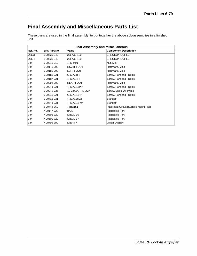
Parts Lists 6-79
SR844 RF Lock-In Amplifier
Final Assembly and Miscellaneous Parts List
These parts are used in the final assembly, to put together the above sub-assemblies in a finished unit.
Final Assembly and Miscellaneous Ref. No. SRS Part No. Value Component Description
U 303 3-00639-342 256KX8-120 EPROM/PROM, I.C.
U 304 3-00639-342 256KX8-120 EPROM/PROM, I.C.
Z 0 0-00045-013 4-40 MINI Nut, Mini
Z 0 0-00179-000 RIGHT FOOT Hardware, Misc.
Z 0 0-00180-000 LEFT FOOT Hardware, Misc.
Z 0 0-00185-021 6-32X3/8PP Screw, Panhead Phillips
Z 0 0-00187-021 4-40X1/4PP Screw, Panhead Phillips
Z 0 0-00204-000 REAR FOOT Hardware, Misc.
Z 0 0-00241-021 4-40X3/16PP Screw, Panhead Phillips
Z 0 0-00248-026 10-32X3/8TRUSSP Screw, Black, All Types
Z 0 0-00315-021 6-32X7/16 PP Screw, Panhead Phillips
Z 0 0-00415-031 4-40X1/2 M/F Standoff
Z 0 0-00641-031 4-40X3/16 M/F Standoff
Z 0 3-00744-360 74HC151 Integrated Circuit (Surface Mount Pkg)
Z 0 7-00147-720 BAIL Fabricated Part
Z 0 7-00508-720 SR830-16 Fabricated Part
Z 0 7-00509-720 SR830-17 Fabricated Part
Z 0 7-00708-709 SR844-4 Lexan Overlay

Parts Lists
SR844 RF Lock-In Amplifier
6-80
Schematic Diagrams