
Model 220 Programmable Current Source Instruction Manual
62
Model 220 Programmable Current Source Instruction Manual A GREATER MEASURE OF CONFIDENCE
Transcript of Model 220 Programmable Current Source Instruction Manual

Model 220 Programmable Current SourceInstruction Manual
A G R E A T E R M E A S U R E O F C O N F I D E N C E

WARRANTY
Keithley Instruments, Inc. warrants this product to be free from defects in material and workmanship for a period of 1 yearfrom date of shipment.
Keithley Instruments, Inc. warrants the following items for 90 days from the date of shipment: probes, cables, rechargeablebatteries, diskettes, and documentation.
During the warranty period, we will, at our option, either repair or replace any product that proves to be defective.
To exercise this warranty, write or call your local Keithley representative, or contact Keithley headquarters in Cleveland, Ohio.You will be given prompt assistance and return instructions. Send the product, transportation prepaid, to the indicated servicefacility. Repairs will be made and the product returned, transportation prepaid. Repaired or replaced products are warranted forthe balance of the original warranty period, or at least 90 days.
LIMITATION OF WARRANTY
This warranty does not apply to defects resulting from product modification without Keithley’s express written consent, ormisuse of any product or part. This warranty also does not apply to fuses, software, non-rechargeable batteries, damage frombattery leakage, or problems arising from normal wear or failure to follow instructions.
THIS WARRANTY IS IN LIEU OF ALL OTHER WARRANTIES, EXPRESSED OR IMPLIED, INCLUDING ANYIMPLIED WARRANTY OF MERCHANTABILITY OR FITNESS FOR A PARTICULAR USE. THE REMEDIES PRO-VIDED HEREIN ARE BUYER’S SOLE AND EXCLUSIVE REMEDIES.
NEITHER KEITHLEY INSTRUMENTS, INC. NOR ANY OF ITS EMPLOYEES SHALL BE LIABLE FOR ANY DIRECT,INDIRECT, SPECIAL, INCIDENTAL OR CONSEQUENTIAL DAMAGES ARISING OUT OF THE USE OF ITSINSTRUMENTS AND SOFTWARE EVEN IF KEITHLEY INSTRUMENTS, INC., HAS BEEN ADVISED IN ADVANCEOF THE POSSIBILITY OF SUCH DAMAGES. SUCH EXCLUDED DAMAGES SHALL INCLUDE, BUT ARE NOT LIM-ITED TO: COSTS OF REMOVAL AND INSTALLATION, LOSSES SUSTAINED AS THE RESULT OF INJURY TO ANYPERSON, OR DAMAGE TO PROPERTY.
Keithley Instruments, Inc.
28775 Aurora Road • Cleveland, Ohio 44139 • 440-248-0400 • Fax: 440-248-6168
1-888-KEITHLEY (534-8453) • www.keithley.com
Sales Offices:
BELGIUM:
Bergensesteenweg 709 • B-1600 Sint-Pieters-Leeuw • 02-363 00 40 • Fax: 02/363 00 64
CHINA:
Yuan Chen Xin Building, Room 705 • 12 Yumin Road, Dewai, Madian • Beijing 100029 • 8610-82251886 • Fax: 8610-82251892
FINLAND:
Halsuantie 2 • 00420 Helsinki, Finland • 09-5306-6560 • Fax: 09-5306-6560
FRANCE:
3, allée des Garays • 91127 Palaiseau Cédex • 01-64 53 20 20 • Fax: 01-60 11 77 26
GERMANY:
Landsberger Strasse 65 • 82110 Germering • 089/84 93 07-40 • Fax: 089/84 93 07-34
GREAT BRITAIN:
Unit 2 Commerce Park, Brunel Road • Theale • Berkshire RG7 4AB • 0118 929 7500 • Fax: 0118 929 7519
INDIA:
1/5 Eagles Street • Langford Town • Bangalore 560 025 • 080 212 8027 • Fax: 080 212 8005
ITALY:
Viale San Gimignano, 38 • 20146 Milano • 02-48 39 16 01 • Fax: 02-48 30 22 74
JAPAN:
New Pier Takeshiba North Tower 13F • 11-1, Kaigan 1-chome • Minato-ku, Tokyo 105-0022 • 81-3-5733-7555 • Fax: 81-3-5733-7556
KOREA:
2FL., URI Building • 2-14 Yangjae-Dong • Seocho-Gu, Seoul 137-888 • 82-2-574-7778 • Fax: 82-2-574-7838
NETHERLANDS:
Postbus 559 • 4200 AN Gorinchem • 0183-635333 • Fax: 0183-630821
SWEDEN:
c/o Regus Business Centre • Frosundaviks Allé 15, 4tr • 169 70 Solna • 08-509 04 600 • Fax: 08-655 26 10
TAIWAN:
13F-3, NO. 6, Lane 99, Pu-Ding Road, Hsinchu, Taiwan, ROC. • 886-3-572-9077• Fax: 886-3-572-9031
4/03

Model 220 Programmable Current Source Instruction Manual-
01982, Keithley Instruments, Inc.
All rights reserved. Cleveland, Ohio, U.S.A.
Eighth Printing, August 2000 Document Number: 220-901-01 Rev. H
Manual Print History
The print history shown below lists the printing dates of all Revisions and Addenda created for this manual. The Revision Level letter increases alphabetically as the manual undergoes subsequent updates. Addenda, which are released between Revisions, contain important change information that the user should incorporate immediately into the manual. Addenda are numbered sequentially. When a new Revision is created, all Addenda associated with the previous Revision of the manual are incorporated into the new Revision of the manual. Each new Revi- sion includes B revised copy of this print history page.
Revision G (Document Number 220-901-01) .............................................................. 1992
Revision H (Document Number 220-901-01) .................................................. August2000

Safety Precautions
The following safety precautions should be observed before using this product and any associated instrumentation. Although some instruments and accessories would normally be used with non- hazardous voltages, there are situations where hazardous conditions may be present.
This product is intended for use by qualified personnel who mcog- nize shock hazards and are familiar with the safety precautions m- quired to avoid possible injury. Read the operating information carefully before using the product.
The types of product users are:
Responsible body is the individual or group responsible for the use and maintenance of equipment. for ensuring that the equipment is operated within its specifications and operating limits, and for en- suring that operators are adequately trained.
Operators use the product for its intended function. They must be trained in electrical safety procedures and proper use of the instn- mat. They must be protected from electric shock and contact with hazardous live circuits.
Maintenance personnel perform mutine procedures on the product to keep it operating, for example, setting the line voltage or replac- ing consumable materials. Maintenance procedures are described in the manual. The procedures explicitly state if the operator may per- form them. Othenvise, they should be performed only by service p~~SONE1.
Service personnel are trained to work on live circuits, and perform safe installations and repairs of pmducts. Only properly trained ser- vice personnel may perform installation and service procedures.
Exercise extreme caution when a shock hazard is present. Lethal voltage may be present on cable connector jacks or test fixtures. The American National Standards Institute (ANSI) states that a shock hazard exists when voltage levels greater than 30V RMS. 42.4V peak, or 60VDC are present. A good safety practice is to expect that hazardous voltage is present in any unknown circuit before tllLXSU~i”g.
Users of this product must be protected from electric shock at all times. The responsible body must ensure that users are prevented access and/or insulated from every connection point. In some cases, connections must be exposed to potential human contact. Product users in these circumstances must be trained to protect themselves from the risk of electric shock. If the circuit is capable of operating at or above 1000 volts, no conductive part of the circuit may be exposed.
As described in the lntemational Electrotechnical Commission (IEC) Standard IEC 664, digital multimeter measuring circuits (e.g., Keithley Models l75A, 199,2000,2001, 2002, and 2010) arc Installation Category II. All other instruments signal terminals are Installation Category I and must not be connected to mains.
Do not connect switching cards directly to unlimited power circuits. They are intended to be used with impedance limited sources. NEVER connect switching cards directly to AC mains. When con- necting sources to switching cards, install protective devices to lim- it fault cormnt and voltage to the card.
Before operating an instrument, make sure the line cord is coonect- ed to a properly grounded power receptacle. Inspect the connecting cables, test leads, and jumpers for possible wear, cracks, or breaks before each use.
For maximum safety, do not touch the product, test cables, or any other insh’oments while power is applied to the circuit under test. ALWAYS remove power from the entire test system and discharge any capacitors before: connecting or disconnecting cables or jump- ers, installing or removing switching cards, or making internal changes, such as installing or removing jumpers.
Do not touch any object that could provide a current path to the common side of the circuit under test or power line (earth) ground. Always make measurements with dry hands while standing on a dry, insulated surface capable of withstanding the voltage being measured.
The instrument and accessories must be used in accordance with its specifications and operating instructions or the safety of the equip- ment may be impaired.
Do not exceed the maximum signal levels of the instruments and ac- cessories, as defined in the specifications and operating infonna- don, and as shown on the instrument or test fixture panels, or switching card.
When fuses are used in a product, replace with same type and rating for continued protection against fire hazard.
Chassis connections must only be used as shield connections for measuring circuits, NOT as safety earth ground connections.
If you are using a test fixture, keep the lid closed while power is a.p- plied to the device under test. Safe operation requires the use of a lid interlock.
Ifa@ screw is present, connect it to safety earth ground using the wire recommended in the user documentation.
Then symbol on an instrument indicates that the user should E- fer to the operating instructions located in the manual.
me A. symbol on an instrument shows that it can source or mea- sure 1000 volts or more, including the combined effect of normal and common mode voltages. Use standard safety precautions to avoid personal contact with these voltages.
The WARNING heading in a manual explains dangers that might result in personal injury or death. Always read the associated infor- mation very carefully before performing the indicated procedure.
The CAUTION heading in a manual explains hazards that could damage the instrument. Such damage may invalidate the warranty.
Instrumentation and accessories shall not be connected to humans.
Before performing any maintenance, disconnect the line cord and all test cables,
To maintain protection from electric shock and fire, replacement components in mains circuits, including the power transformer, test leads, and input jacks, must be purchased from Keithley Instn- mats. Standard fuses, with applicable national safety approvals, may be used if the rating and type are the same. Other components that are not safety related may be purchased from other suppliers as long as they are equivalent to the original component. (Note that se- lected parts should be purchased only through Keithley Instruments to maintain accuracy and functionality of the product.) If you are un~tre about the applicability of a replacement component, call a Keithley Instruments office for information.
To clean an instrument, use a damp cloth or mild, water based cleaner. Clean the exterior of the instrument only. Do not apply cleaner directly to the instrument or allow liquids to enter or spill on the instrument. Products that consist of a circuit board with no case or chassis (e.g., data acquisition board for installation into a computer) should never require cleaning if handled according to in- structions. If the board becomes contaminated and operation is af- fected, the hoard should be returned to the factmy for proper cleaning/setvicing.
Rev. IO/99

MODEL 220 SPECIFICATIONS
IEEE-488 BUS IMPLEMENTATION

TABLE OF CONTENTS
Paragraph Title Page
SECTION l-GENERAL INFORMATION 1.1 Introduction .................................... 1.2 Features ........................................ 1.3 Warranty Information ............................ 1.4 ManualAddenda ................................ 1.5 Safety Symbols and Terms ........................ 1.6 Unpacking and Inspection ......................... 1.7 Repackaging For Shipment ........................ 1.8 Specifications ................................... 1.9 Accessories ..................................... 1.9.1 Optional Accessories ........................... 1.9.2 Supplied Accessories. ..........................
SECTION 2-OPERATION 2.1 Introduction ................................... 2.2 Preparation For Use ............................. ^^_ -
......
......
......
......
......
......
......
......
......
......
......
..........
..........
..........
..........
..........
..........
..........
..........
.......
.......
.......
.......
.......
.......
.......
.......
.......
.......
.......
......
......
......
......
......
......
......
......
......
......
......
L.L.1
..,... .._.
2.2.2 2.3 2.3.1 2.3.2 ,2.3.3 2.3.4 2.3.5 2.4 2.4.1 2.4.2 2.5 2.5.1 2.5.2 2.5.3
,..... .................. ..................
vower-up ............................................................................ Warm-Up .............................................................................
Operating Instructions .................................................................... Environmental Conditions ............................................................... Front Panel Control Descriptions .......................................................... AearPanelDescriptions ................................................................. OutputConnector ..................................................................... InductiveLoads .......................................................................
Operation Of The Model 220. .............................................................. Model 220 General Operating Procedure .................................................. ExampleofOperation ...................................................................
Applications ............................................................................ Calibradon ............................................................................ ResistivityMeasurement ................................................................ Diode Characterization .................................................................
......
......
......
......
......
......
....
2-1 2-1 2-l 2-l 2-l 2-1 2-1
;=t 2-4 2-5 2-5 2-5 ......
...... 2-9
...... 2-9
...... 2-9
..... 2-10
l-l l-l l-l 1-l 1-l l-l l-l l-l 1-2 1-2 1-2
SECTION 3-PERFORMANCE VERIFICATION 3.1 Introduction .................................................................................. 3.2 Environmentalconditions ....................................................................... 3.3 RecommendedTestEquipment .................................................................. 3.4 InitialCondltlons ...............................................................................
El Performance Verification Procedure ..............................................................
lOOmA to 1mA Range Verification .............................................................. 3.5.2 1004 to 1OlA Range Verification .............................................................. 3.5.3 1FA end lOOnA Range Verification. ............................................................. 3.5.4 1OnA and 1nA Range Verification ...............................................................
SECTION 4-THEORY OF OPERATION 4.1 Introduction .................................................................................. 4.2 BlockDiagrams ................................................................................ 4.3 PowerSupply ................................................................................. 4.4 AnalogBoard.. ................................................................................ 4.5 Digital Board (Microcomputer). .................................................................. 4.6 DisplaVCircuit .................................................................................
3-l 3-l 3-l 3-1 3-1 3-1 3-2 3-2 33
4-1 41 4-l 41 4-4 4-4
i
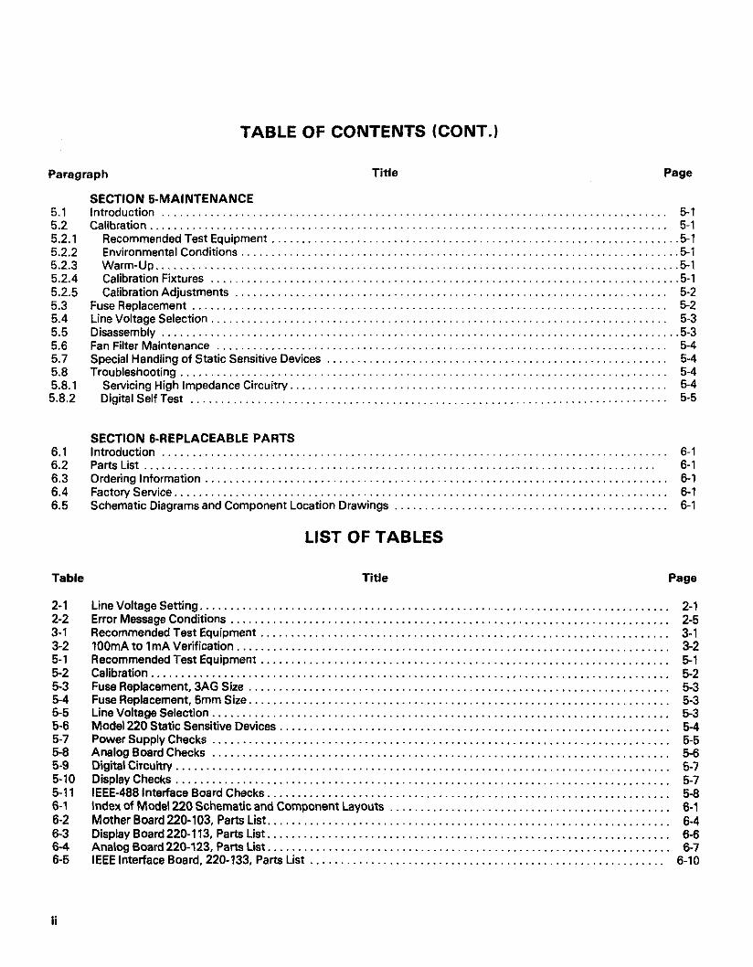
TABLE OF CONTENTS (CONT.1
Paragraph Title Page
SECTION S-MAINTENANCE 5.1 Introduction ............................ 5.2 Calibration .............................. 5.2.1 Recommended Test Equipment .......... 5.2.2 Environmental Conditions ............... 5.2.3 Warm-Up ............................. 5.2.4 Calibration Fixtures .................... 5.2.5 Calibration Adjustments ................ 5.3 Fuse Replacement ....................... 5.4 Line Voltage Selection .................... 5.5 Disassembly ............................ 5.6 Fan Filter Maintenance ................... 5.7 Special Handling of Static Sensitive Devices 5.8 Troubleshooting ... ..................... 5.8.1 Servicing High Impedance Circuitry. ...... 5.8.2 Digital Self Test .......................
.
. . . .
,
.5-l . ...5-1
5-2 5-2 5-3
SECTION B-REPLACEABLE PARTS 6.1 Introduction ._.,,.......,..___......_..........._._..._._....._....._.......................... 6-l 6.2 PartsList..................................................................................... 6-l 6.3 Ordeilnglnformation...................................................................,,......, 6-l 6.4 FactoryService..........................................................................,...,.. 6-l 6.5 Schematic Diagrams and Component Location Drawings 6-l
LIST OF TABLES
Table Title Page
2-1 2-2 3-1 3-2 5-1 5-2 5-3 54 5-5 5-6 5-7 5-8 5-9 5-10 5-11 6-l 6-2 6-3 6-4 6-5
ii
LineVoltageSetting ................................................. Error Message Conditions ............................................ Recommended Test Equipment ....................................... lOOmA to 1mA Verification ........................................... Recommended Test Equipment ....................................... Calibration ......................................................... Fuse Replacement, 3AG Size ......................................... Fuse Replacement, 5mm Size ......................................... Line Voltage Selection ............................................... Model 220 Static Sensitive Devices .................................... Power Supply Checks ............................................... AnalogBoardChecks ............................................... DigitalCircuitry ..................................................... DisplayChecks ..................................................... IEEE-488 Interface Board Checks ...................................... Index of Modal 220 Schematic and Component Layouts .................. Mother Board 220-103, Parts List. ..................................... Display Board 220-l 13, Parts List. ..................................... Analog Board 220-123, Parts List. ..................................... IEEE Interface Board, 220-133. Parts List ...............................
........................... 2-1
........................... 2-5
........................... 3-1
........................... 3-2
........................... 5-1
........................... 5-2
........................... 5-3
...........................
........................... z
...........................
........................... E
...........................
........................... 2
........................... 5-7
........................... 5-8
........................... 6-l
........................... 6-4
........................... 6-6
........................... 6-7
.......................... 6-10
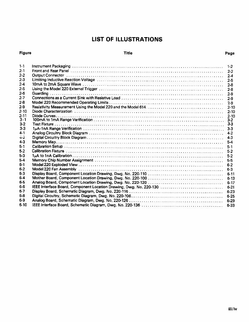
LIST OF ILLUSTRATIONS
Figure Title Page
l-l 2-1 2-2 2-3 2-4 2-5 2-6 2-7 2-8 2-9 2-10 2-11 3-1 3-2 3-3 4-1 -i-i 4-3 5-l 5-2 5-3 5-4 6-l 6-2 6-3 6-4 6-5 6-6 6-7 6-8 6-9 6-10
Instrument Packaging ....................................... FrontandRearPanel ........................................ OutputConnector .......................................... Limiting Inductive Reaction Voltage ........................... lOmAto2mASquareWave .................................. Using the Model 220 External Trigger .......................... Guarding .................................................. Connections es a Current Sink with Resistive Load ............... Model 220 Recommended Operating Limits ..................... Resistivity Measurement Using the Model 220 end the Model 614 Diode Characterization ......................................
............ ............ ............ ............ ............ ............ ............ ............ ............ ............ ............
...... 1-2 ...... 2-2 ...... 2-4 ...... 2-5 ...... 2-8 ...... 2-8 ...... 2-9 ...... 2-9 ...... 2-9 ...... 2-10 ...... Z-10
DiodeCurves .................................................................................. 2-10 lOOmA to 1mA Range Verification ................................................................ 3-2
3-3 3-3 4-2
Test Fixture.. ................................................................................. lFA-1nARangeVerification ..................................................................... Analog Circuitry Block Diagram .................................................................. Digital Circuitry Block Diagram ................................................................... MemonlMap .................................................................................. CalibrationSetup.. ............................................................................ Calibration Fixture ............................................................................. l~tolnACalibration...................................................: ...................... MemoryChipNumberAssignment ............................................................... Model220ExplodedView ....................................................................... Model220FanAssembly ....................................................................... Display Board, Component Location Drawing. Dwg. No. 220-l 10 ..................................... Mother Board, Component Location Drawing, Dwg. No. 220-100 ..................................... Analog Board, Component Location Drawing, Dwg. No. 220-120 ..................................... IEEE Interface Board, Component Location Drawing, Dwg. No. 220-130 ............................... Display Board, Schematic Diagram, Dwg. No. 220-l 16 .............................................. Digital Circuitry, Schematic Diagram, Dwg. No. 220-106. ............................................ Analog Board, Schematic Diagram, Dwg. No. 220-126 .............................................. IEEE Interface Board, Schematic Diagram, Dwg. No. 220-136 ........................................
4-3 5-4 5-1 5-2 5-2 5-5 6-2 6-3 6-11 6-13 6-17 6-21 6-23 6-25 6-29 6-33
iii/iv

SECTION 1 GENERAL INFORMATION
1.1 INTRODUCTION
The Model 220 is a programmable current source with full range current from 2nA to 100mA. The Model 220 has a selectable voltage compliance of up to 105V in one volt in- crements. The 100 memory locations allow up to 100 storage points for programming source, V-limit, end dwell time. The Model 220 can be used with any measurement system that uses the IEEE-488 interface bus. For detailed operating instructions of the Model 220 end the IEEE-488 bus, refer to the Model 220/230 Programming Manual.
1.2 FEATURES
The Model 220 includes the following features:
100 point buffer that is capable of storing up to 100 points of an output waveform. Programmable dwell time between the data points in the buffer when used in the single or continuous program modes. Input end output connections for external triggering located on the rear panel. Selectable voltage compliance allows operator to select the required voltage compliance. 4% digit display with appropriate exponent and decimal point. Program modes that control the sequence between the buffer points. This is for either single, step or continuous sequencing. Data keyboard to enter data (V-limit, dwell time, source, etc.1 into the buffer.
l Program control that has a start, stop end reset control for the buffer end program mode.
. OPERATE button that holds the source in standby until programmed into operate.
l IEEE-488 interface bus operation isstandard. Thisenables the Model 220 to be incorporated into a system that uses programmed control through the IEEE-488 bus.
1.3 WARRANTY INFORMATION
Warranty information is provided on the inside front cover of this manual. If there is a need to exercise the warranty, contact the Keithley representative in your area to deter- mine the proper action to be taken. Keithley maintains corn- plete repair and calibration facilities in the United States, West Germany, Great Britain, France, the Netherlands, Switzerland end Austria. Information concerning the appli- cation, operation or service of your instrument may be directed to the applications engineer et any of the above locations. Check the inside front cover of this manual for addresses.
1.4 MANUAL ADDENDA
Improvements or changes to this manual will be explained on en addendum included with this manual.
1.5 SAFETY SYMBOLS AND TERMS
Safety symbols used in this manual are as follows:
The symbol A on the instrument denotes that the user should refer to the operating instructions.
The symbol on the instrument denotes that 1OOOV or more may be present on the terminal(s).
The WARNING used in this manual explains dangers that could result in personal injury or death.
The CAUTION used in this manual explains hazards that could damage the instrument.
1 .6 UNPACKING AND INSPECTION
The Model 220 is inspected both mechanically and elec- trically before shipment. Upon receiving the Model 220 unpack all items from the shipping container and check for any obvious damage that may have occurred during transit. Report any damage to the shipping agent. Retain end use the original packaging materials if reshipment is necessav. The following items are shipped with all Model 220 orders: *Model 220 Programmable Current Source *Model 220 Instruction Manual *Model 6011 Triaxial Test Lead *Model 220/230 Programming Manual *Optional accessories per request.
1.7 REPACKAGING FOR SHIPMENT
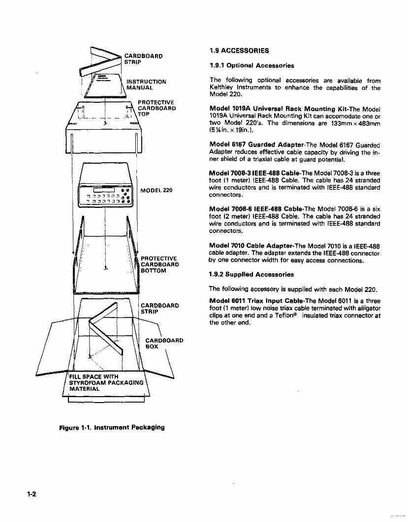
The Model 220 should be packed in its original carton using the packaging method shown in Figure l-l. Before pack- aging, wrap the instrument in plastic. After it is placed in the box, surround the instrument with Styrofoam packaging material.
If the Model 220 is to be returned to Keithley Instruments for calibration or repair, include the following: *ATTENTION REPAIR DEPARTMENT on the address label. *Warranty status of the instrument. *Completed service form.
1.8 SPECIFICATIONS
For Model 220 detailed specifications, refer to the specifica- tions that precede this section.
l-l
INSTRUCTION
!FIL ST MI
‘ROTECTIVE :ARDSOARD rap
MODEL 220
PROTECTIVE CARDBOARD BOHOM
YROFOAM PACKAGING 4TERIAL
CARDBOARD STRIP
-7 CARDBOARD BOX ,
1.9 ACCESSORIES
1.9.1 Optional Accessories
The following optional accessories are available from Keithley Instruments to enhance the capabilities of the Model 220.
Model 1019A Universal Rack Mounting Kit-The Model 1019A Universal Rack Mounting Kit can accomodate one or two Model 220’s. The dimensions are 133mm x 483mm (5%in. x 19in.I.
Model 8167 Guarded Adapter-The Model 8167 Guarded Adapter reduces effective cable capacity by driving the in- ner shield of a triaxial cable at guard potential.
Model 7008-3 IEEE-468 Cable-The Model 7008-3 is a three foot I1 meter) IEEE488 Cable. The cable has 24 stranded wire conductors and is terminated with IEEE-488 standard connectors.
Model 70089 IEEE-488 Cable-The Model 7008-6 is a six foot I2 meter) IEEE-488 Cable. The cable has 24 stranded wire conductors and is terminated with IEEE-488 standard connectors.
Model 7010 Cable Adapter-The Model 7010 is a IEEE-488 cable adapter. The adapter extends the IEEE-488 connector by one connector width for easy access connections.
1.9.2 Supplied Accessories
The following accessory is supplied with each Model 220.
Model 8011 Triax Input Cable-The Model 8011 is a three foot (1 meter1 low noise triax cable terminated with alligator clips at one end and a Teflon0 insulated triax connector at the other end.
Figure 1-l. Instrument Packaging
I-2

SECTION 2 OPERATION
2.1 INTRODUCTION
This section includes operating instructions such as: prepara- tion for use, environmental conditions, front and rear panel control descriptions, output connections and several examples of uass and applications of the Model 220. For Model 220 front and rear panel illustrations refer to Figure 2-l.
2.2 PREPARATION FOR USE
2.2.1 Power-Up
Plug the Model 220 into the proper power receptacle in accor- danca with Table 2-l. For fuss replacement or line switch lS102j setting refer to the maintenance section.
WARNING Ground the instrument through a properly aarth grounded racaptacla before operation. Failure to ground the instrument can result in severe injury or death in the avant of short circuit or malfunction.
Table 2-1. Line Voltage Setting
Input Voltage Switch Setting Fuse IFlOlj 5102
105V-125V I15VAC %A. 25OV. 3AG 21OV25OV 230VAC %A, 25OV. 3AG
9ov-1lOV’ 116VAC ‘%A, 25OV. 3AG 18OV22OV’ 230VAC %A, 25OV. 3AG
“For instrumenta equipped with low voltage transformer TR-187.
Immediately after turning on the Model 220 via the power switch, the display will indicate the followfng for several seconds:
1. This ia a diiplay teat. The opsretor can nota inoperative diiplay aegmenh by comparing the Model 220’s display wfth tha figure above.
2. In addition, the push button and the TALK, LISTEN, REMOTE indicators will light. All indicators will light simultaneously if operating correctiy.
After ths display teat is complete the Model 220 will dkplay the software revision level for approximately ona second.
Emmp’e: /
After the software revision level is displayed, the Model 220 will display ths primary address of the instrument for approx- imately one second. The primary address of the Model 220 is factory set at 12.
Example: j f I I I?
I
2.2.2 Warm-Up
To achieve rated accuracy the Model 220 requires one hour for warm-up.
2.3 OPERATING INSTRUCTIONS
2.3.1 Environmental Conditions
Operation of the Model 220 should ba at an ambient temperature within the range of O°C to 5O’C. up to 35°C at 70% noncondensing relative humidity. Environmental condi- tions for storage are from -25OC to +70°C.
2.3.2 Front Panel Controls Description
Power On/Dff switch operates on the push-push principle. Depressing this button turns the instrument on. Pushing the button again heleasingl turns the instrument off.
Display-There are four operating functions in the display group. They are deacribad as follows.
SOURCE button selecta the source data for display. The full Scala range of the available source current is 1.9995nA to lOl.OOmA. The source current is displayed as a 4% digit number with a single digit exponent. The least significant digit of the 4’% digit diiplay is truncated to a “0” or a “5” when the ENTER button is pressed. When a 1,2,3 or 4 is entersd ss the least Signifiwnt digit, it is truncated to a zero when the ENTER button is praaaed. When a 6, 7,8 or 9 is entered as the least significant digit, it is truncated to a five when the ENTER but- ton is pressed.
During the entry of source data onto the display (cursor is flashing), pressing the SOURCE button reverta the display to the prekus source data. A different source current can be programrr& for each of the 100 memory locations.
V-LIMfT bumn selecta the voltage compliance for display. The compliance voltage ranges from 1V to 105V in 1V in- crements. The voltage compliance is displayed as a thrss digit number. The three digit number is right justified when a one or two digit number is entered and the ENTER button is pressed. The voltage compliance limiting is bipolar.
The vokage limit accuracy for output current (I,,) greater than 1nA and Issa than 1004 is f 3%1+05V). For lDyt greater than Or equal to 1OOfi there is an additional error of 1V in the seme
2-1

/ \
Figure 2-1. Model 220 Front and Rear Panels
2-2
polarity of lout. For IOU, less than or equal to 1nA there is an ad- ditional error of 0.5V with the opposite polarity of laut
A different compliance voltage limit can be programmed for each of the 100 memory locations. During the entry of V-limit data onto the display, lcuraor is flashing) pressing the V-LIMIT button reverts the display to the previous V-limit data. DWELL TIME button selects the dwell time data for display. Dwell time is defined as the programmed time the Model 220 spends on a specific memory location when in the single or continuous program modes. The range of the dwell time is 3msec to SSS.%?c. The dwell time is displayed as a 4% digit number with a single digit exponent. After the data is entered onto the display and the ENTER button is presaad, the expo- nent is displayed as a -3 or a 0 depending on the data entered. An entry of zero for the dwell time, in any memory location ex- cept the first will be interpreted as a reset in the step or con- tinuous program modes to permit short cycling of the pro grammed memory locations it will be interpreted as a stop in the single program mode. The dwell time accuracy listed in the specifications requires that the IEEE-488 bus to be inactive.
A different dwell time can be programmed for each of the 100 memory locations. During the entry of dwell time data onto the displaY (cursor is flashing), pressing the DWELL TIME button reverts the display to the previous dwell time data.
MEMORY button selects the present memory location number for display. There are 100 available memory locations. They start at memory location 1 and range up to Iscation 100. The memory location is displayed es a thraa digit number. The three digit display is right justified when a one or two digit number is enterned onto the display or upon actuation of the RESET button the Model 220 selects memory location 1 as the present memory location.
Each memory location contains the source current data, V-limit data, dwell time data and tha number of the memory location. To display any of these parameters contained in a particular memory location simply press the appropriate button (eg. SOURCE, V-LIMIT, DWELL TIME or MEMORY). The data of each of these parameters can vary for each memory location. This means the Model 220 can store up to 100 different values of source current, compliance voltage or dwell time
During the entry of memory location data onto the display (cursor is flashing), pressing the MEMORY button reverts the display to the previously displayed memory location.
NOTE The contents of all the msmon/ locations are lost when the power to the Model 220 is turned off.
Data Entry-The three buttons contained in the data entry group consist of the COPY, ENTER and EXPONENT buttons. The three buttons and their functions are described as follows: EXPONENT button allows entry of exponent data onto the display. The 5XPONENT button is active only in the source and dwell time display modes. Once the single digit exponent
data has bean entered onto the display and the ENTER button is pressed, the Model 220 places the data and the exponent in- to the proper notation For example, if 520.0-7 is entered on the display, it is displayed as 52.00-6 after the ENTER button is pressed. ENTER button loads the displayed data into the present memory location. COPY button duplicates the source, V-limit, and dwell time data from one memory location into the next memory location. The COPY button is active only in the memory display mode. Refer to example 5.
OUTPUT button is an alternate action control which places the instrument in the displayed output mode. In the operate mode, the OUTPUT LED is turned on and the source data in the present memory location is present at the output connec- tor on the rear panel. When the instrument is not in the operate mode, the output is programmed to .0000-S amps.
Additionally if the compliance voltage was programmed to >32V it will be reduced (without changing displayed value) to 32V.
Program Mode-The three buttons contained in the program mode group consist of the SINGLE, CONTINUOUS and STEP buttons. These three buttons select the possible modes of scanning the internal 100 memory locations. The bunons are described as follows: STEP button selects the step program mode. The step pro- gram mode allows the user to manually step through the pro- grammed memory locations using the START/STOP button. When the Model 220 is in the step program mode the STEP LED is turned on. SINGLE button selects the single program mode. The single program mode cycles through the programmed memory loca tions one time upon the actuation of the START/STOP but- ton. When the Model 220 is in the single program mode the SINGLE LED is turned on. CONTINUOUS button selects the continuous program mode. The continuous program mode cycles through the programm- ed memory locations continuously upon the actuation of the START/STOP button. When the Model 220 is in the con- tinuous program mode ths CONTINUOUS LED is tumad on.
Program Control-The two buttons contained in the pro- gram control group are the RESET and START/STOP but- tons. These two bunons control the use of the single, con- tinuous and step program modes. The two buttons are described as follows:
RESET button is a momentary control that sets the presently displayed memory location back to memory location 1. If the Model 220 is in the operate mode, pressing the RESET button sets the output to tha source data located in memory location 1. Pressing the RESET button during the entry of data onto the display in the Source, V-limit, dwell time or memory display modes sets the display back to the previous displayed data. Once the data is entered onto the display and the ENTER but- ton is pressed, pressing the RESET button reverts the instru- ment back to the conditions in memory location 1.
2-3

START/STOP button is an alternate action control that serves two functions. The two functions are described as follows: 1. When the START/STOP button is pressed the selected pro
.gram mode (step, single or continuous) is initiated. 2. When the START/STOP button is pressed a second time
the START/STOP and the action of the selected program mode is stopped.
3. The START/STOP LED will be on continuously during the execution of the single of continuous program mode. In the step program mode the LED will be on the duration of the programmed dwell time.
NOTE When the instrument is in the standby mode (OPERATE LED is turned off), and either single or continuous programming mode, the START/ STOP button continues to control the buffer with no output present on the Model 220. In the step mode, the START/STOP LED turns on for the duration of the programmed dwell time.
DATA-The 12 buttons in the Data group allow entry of numerical data from 0 to 9 including with decimal point and polarity onto the display,
The TALK, LISTEN and REMOTE LED’s identify the pre- sent status of the IEEE-488 bus. For more information con- cerning the Model 220 and the IEEE-488 bus refer to the Model 220/230 Programming Manual.
2.3.3 Rear Panel Description
OUTPUT connector is Teflon@ insulated female triax con- nector.
GUARD terminal provides a low impedance voltage source which is equal to the output compliance voltage. The max- imum load oapcitence for the guard output is O.OlhF. The max- imum load current which includes guard and output is not to exceed 106mA. The accuracy of the guard output is f 1mV excluding output lead IR voltage drops.
NOTE The guard voltage will not equal the output voltage when the instrument is at the programm- ed V-limit overcompliance level.
DIGITAL l/O port consists of four input end four output lines as well as IEEE-488 common and +5VDC. The outputs will drive one TTL load. The instrument can be programmed to generate an SRQ upon any change in the 4 bit input data.*
EXTERNAL TRIGGER INPUT initiates the selected program mode in the same manner as the START/STOP button upon receiving a TTL level negative transition with a minimum pulse width of lO@ec.
EXTERNAL TRIGGER OUTPUT provides a negative TTL level pulse of greater than lO@ec at the completion of the pro- grammed dwell time.
The line power fuse is rated as shown in Tables 52 and 53.
The line plug mates with a 3-wire line cord which provides UL approved connections to line power.
*For more information concerning the IEEE488 connector, digital I/D port and primary address switches refer to the Model 220/230 Programming Manual.
2.3.4 Output Connector
The output connector is a Teflon@ insulated triax connector which is located on the rear panel. The maximum allowable voltage potential between the HI terminal and the LO terminal is f 1OOV. The maximum allowable common mode voltage between the HI input terminal and the chassis common is 25OVrms DC to 60Hz. See Figure 2-2.
CAUTION Do not exceed the maximum common mode voltage. Instrument damage may occur.
OUTPUT COMMON terminal provides easy access to output common which is also the inner shield of the output connec-
Figure 2-2. Output Connector
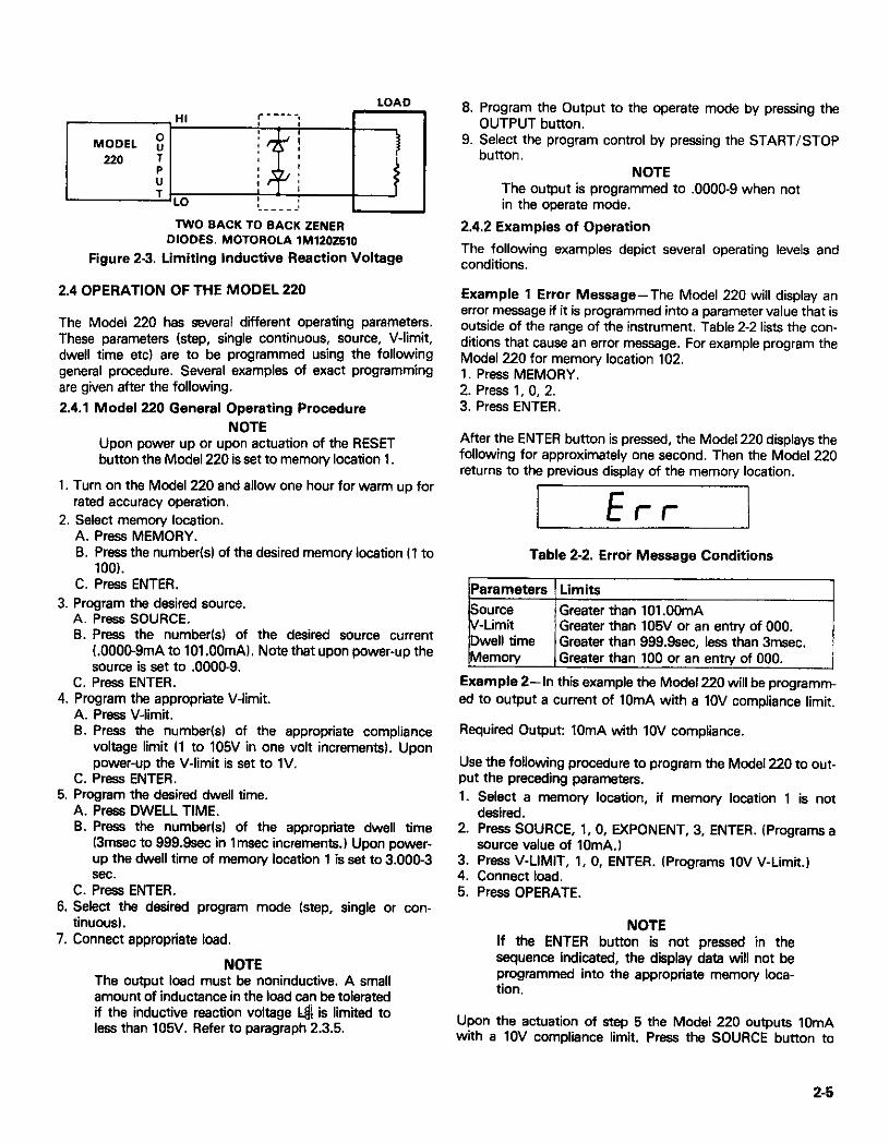
tor. 23.5 Inductive Loads
mvenient connec- In general, the output load connected to the Model 220 should be resistive. However, a small amount of inductance in the load can be tolerated but only if the inductive reaction voltage
IEEE-W INTERFACE connector provides bus connection to L&is limited to less than 105V. Refer to Figure 2-3 for a sug-
the Model 220. The connector mates with the Model 70083 gested method of limiting the inductive reaction voltage.
and 70066 IEEE cables.*
AYY~CJJ swrcnes are use0 10 program me r ADDRESS switches are used to program the primary address for the IEEE-488 interface bus operation. The c for the IEEE-488 interface bus operation. The primary address is “dated only ,._^_ - -...__ .._ * is updated only upon power-up.*
If the output load connected to the Model 220 is inductive, limit the inductive reaction voltage to lass than 106V. Otherwise instru- ment damage may occur.
2-4
8. Program the Output to the operate mode by pressing the
pressing the START/STOP
TWO SACK TO BACK LENER DIODES. MOTOROLA ,hl,20ZS,a
Figure 2-3. Limiting inductive Reaction Voltage
2.4.2 Examples of Operation
The following examples depict several operating levels and conditions.
2.4 OPERATION OF THE MODEL 220
The Model 220 has several diierent operating parameters. These parameters (step, single continuous, source, V-limit, dwell time etc) are to be programmed using the following general procedure. Several examples of exact programming are given after the following.
2.4.1 Model 220 General Operating Procedure NOTE
Upon power up or upon actuation of the RESET button the Model 220 is set to memory location 1.
1. Turn on the Model 220 and allow one hour for warm up for rated accuracy operation.
2. Select memory location. A. Press MEMORY. B. Press the number(s) of the desired memory location (1 to
100). C. Press ENTER.
3. Program the desired source. A. Press SOURCE. 6. Press the numbarks) of the desired source current
(.0000-9mA to lOl.OOmAI. Note that upon power-up the source is sat to .OOOO-9.
C. Press ENTER. 4. Program the appropriate V-limit.
A. Press V-limit. B. Press the number(s) of the appropriate compliance
voltage limit (1 to 105V in one volt increments). Upon power-up the V-limit is set to 1V.
C. Press ENTER. 5. Program the desired dwell time.
A. Press DWELL TIME. B. Press the number(s) of the appropriate dwell time
13msec to 999.9sec in 1 msec increments.) Upon power- up the dwell time of memory location 1 is set to 3.000-3 sec.
C. Press ENTER. 6. Select the desired program mode Istep, single or con-
tinuousl. 7. Connect appropriate load.
NOTE The output load must be noninductive. A small amount of inductance in the load can be tolerated if the inductive reaction voltage L# is limited to less than 105V. Refer to paragraph 2.3.5.
Example 1 Error Message-The Model 220 will display an error message if it is programmed into a parameter value that is outside of the range of the instrument. Table 2-2 lists the con- ditions that cause an error message. For example program the Model 220 for memon/ location 102. 1. Press MEMORY. 2. Press 1, 0, 2. 3. Press ENTER.
After the ENTER button is pressed, the Model 220 displays the following for approximately one second. Then the Model 220 returns to the previous display of the memory location,
/I
Table 2-2. Erroi Message Conditions
Parameters Limits Source / Greater than 101 .OOmA i
-Limit Greater than 105V or an entrY of 000. Dwell time Greater than 999.9sec. less than 3msec. Memory Greater than 100 or an entry of 000.
Example 2-In this example the Model 220 will be programm- ed to output a current of 1OmA with a 1OV compliance limit,
Required Outpur: 1OmA with 1OV compliance.
Use the following procedure to program the Model 220 to out- put the preceding parameters. 1. Select a memory location, if memory location 1 is not
desired. 2. Press SOURCE, 1, 0, EXPONENT, 3. ENTER. (Programs a
source value of 10mA.J 3. Press V-LIMIT, 1, 0, ENTER. (Programs 1OV V-Limit.) 4. Connect load. 5. Press OPERATE.
NOTE If the ENTER button is not pressed in the sequence indicated, the display data will not be programmed into the appropriate marnon/ loca- tion
Upon the actuation of step 5 the Model 220 outputs 1OmA with a 1OV compliance limit. Press the SOURCE button to
2-5
verifY that the 1OmA was actually programmed into the Model 220. Press the V-LIMIT button to verify that the 1OV limit was actually programmed into the Model 220.
Example 3-In this example the Model 220 will be programm- ed to output three separate currents, three separate com- pliance limits, three separate dwell times and three separate memory locations. The three memory locations will be pro- grammed in the step program mode.
Required Output: lOOpA, 1OV V-limit, 1 second dwell time, memory location 1. ImA, 20V V-limit, 1OOmsec dwell time, memory location 2. lOmA, 30V V-limit, 2.5 second dwell time, memon/ location 3.
1. Press MEMORY, 1, ENTER. (Selects memory location 1 .I 2. Press SOURCE, 1, 0, 0, 5XPONENT. 6, ENTER. (Pro-
grams memory location 1 source for 10Oj~A.j 3. PressV-LIMIT, 1, 0, ENTER. (Programs memory location 1
V-limit for 1OV.l 4. Press DWELL TIME, 1, 5XPONENT. 0, ENTER. (Programs
memory location 1 dwell time for one second.) 5. Press MEMORY, 2, ENTER (Selects memory location 2.) 6. Press SOURCE, 1, 5XPONENT. 3, ENTER. (Programs
memory location 2 source for ImA. 7. Press V-LIMIT, 2,0, ENTER. (Programs memory location 2
V-limit for 2OV.j 8. Press DWELL TIME, 1, 0, 0, EXPONENT, + /-, 3, ENTER.
(Programs memory location 2 dwell time for 100msec.j 9. Press MEMORY, 3, ENTER. (Selects memory location 3.1
10. Press SOURCE, 1, 0, 5XPONENT. 3, ENTER. (Programs memory location 3 source for lOmA.)
11. Press V-LIMIT, 3,0, ENTER. (Programs memon/ location 3 V-limit for 30V.J
12. Press DWELL TIME, 2, ., 5, EXPONENT, 0, ENTER. (Pro- grams memory location 3 dwell time for 2.5sec.)
13. Press STEP. (Selects the step program mode.)
After completing step 13 the Model 220 is programmed into the parameters stated. To display any of the three programm- ad source values, select the desired source value’s memon/ location and press the SOURCE button. To output any of the three source values select the desired source value’s memory location, and press the OUTPUT bunon. Pressing the START/ STOP button advances the Model 220 to the next channel. Notice that the START/STOP LED turns on for the program- mad dwell time and then turns off. Note that actuation of START/STOP at memory location 3 will put instrument to location 1.
Example 4-In this example the Model 220 will be programm- ed to output five separate currents, five separate compliance limits, five separate dwell times and five separate memon/ loca- tions.
Required Output: lOOnA, 5V V-limit, 0.5 second dwell time, memory location 1. lfi, 1OV V-limit, 1 second dwell time, memory location 2.
lOti, 15V V-limit, 1.5 second dwell time, memory location 3. loo@!, 20V V-limit, 2 second dwell time, memon/ location 4. lmA, 25V V-limit, 2.5 second dwell time, memory location 5.
1. Press MEMORY, 1, ENTER. (Selects memory location 1.) 2. Press SOURCE, 1, 0, 0, EXPONENT, 9, ENTER. (Pro-
grams memonl location 1 soume for lOOnA. 3. Press V-LIMIT, 5, ENTER. (Programs memory location 1
V-limit for 5V.I 4. Press DWELL TIME, ., 5, 5XPONENT. 0, ENTER. (Pro-
grams memory location 1 dwell time for 0.5 seconds.) 5. Press MEMORY, 2, ENTER. (Selects memory location 2.) 6. Press SOURCE, 1, D(PONENT, 6, ENTER. (Programs
memory location 2 source for 1fi.j 7. Press V-LIMIT, 1, 0, ENTER. (Programs memory location 2
V-limit for 1OV.j 8. Press DWELL TIME, 1, 5XPONENT. 0, ENTER. (Programs
memon/ location 2 dwell time for one second.) 9. Press MEMORY, 3, ENTER. (Selects memory location 3.1
10. Press SOURCE, 1, 0, EXPONENT, 6, ENTER. (Programs memory location 3 soume for lOti.)
11. Press V-LIMIT, 1,5, ENTER. (Programs memon/ location 3 V-limit for 16V.l
12. Press DWELL TIME, 1, ., 5, D(PONENT, 0, ENTER. (Pro- grams memory location 3 dwell time for 1.5 seconds.)
13. Press MEMORY, 4, ENTER. (Selects memory location 4.) 14. Press SOURCE, 1, 0, 0, 5XPONENT. 6, ENTER. (Pro-
grams memory location 4 soume for loo&) 15. Press V-LIMIT, 2,0, ENTER. (Programs memory location 4
V-limit for 2OV.) 16. Press DWELLTIME, 2,5XPONENT, 0, ENTER. (Programs
memory location 4 dwell time for 2 seconds.) 17. Press MEMORY, 5, ENTER. (Selects memory location 5.) 19. Press SOURCE, 1, EXPONENT, 3, ENTER. (Programs
memory location 5 soume for ImA.) 19. Press V-LIMIT, 2,5, ENTER. (Programs memory location 5
V-limit for 25V.) 20. Press DWELL TIMEI, ., 5, EXPONENT, 0, ENTER. (Pro-
grams memon/ location 5 dwell time for 2.5 seconds.)
After completing step 20 the Model 220 is programmed into the parameters stated. To display any of the parameters of any memory location select the desired memory location and then select the desired parameter. To output any of the source valuas select the desired source value’s memory location end press the OUTPUT button.
To scan the five memory locations use the following pro- cedure: 1. Select the program mode of scanning. (Select Single, Con-
tinuous, or Step.1 2. Select desired display mode. (Source, V-limit, dwell time or
memory.) 3. Press the START/STOP bunon.
2-6

In the step program mode the user can manually step through the programmed memory locations one at a time. Each time it is desired to advance to the next programmed memory loca- tion the user presses the START/STOP button. The START/ STOP LED turns on for the duration of the programmed dwell time. When the last programmed memory location is selected fmemory location 5 in this example) pressing the START/ STOP button reverts the instrument to memory location 1.
In the single program mode the Model 220 cycles through all the programmed memory locations one time. To start the single program mode press the START/STOP button. Once the single program mode is activated, the Model 220 starts from the present memory location and advances to each pro- grammed memory location. The instrument remains at each memory location for the programmed dwell time and then ad- vances to the next programmed memory location. After the dwell time of the last programmed location the START/STOP LED turns off and the single program mode is ended. The Model 220 remains at the last programmed location until power is turned off, RESET is pressed, memory location is changed or the single or continuous program modes are ac- tivated.
NOTE An entry of zero for the dwell time for any memory location is interpreted as a reset in the step, single and continuous program modes.
In the continuous program mode the Model 220 cycles through all the programmed mernor~ locations continuously. To start the continuous program mode press the START/ STOP button. To stop the continuous program mode press the START/STOP button a second time. When the START/ STOP button is pressed the second time the continuous pro- gram mode is stopped at the present memory location. Once the continuous program mode is activated, the Model 220 starts from the present memory location and advances to the next memory location. The instrument remains at the present memory location for the programmed dwell time (dwell time can vary for each memory location) and then advances to the next memory location. The cycle continues up to and including the last programmed memory location and then reverts to memarY location 1. At this point the cycle starts over again and keeps repeating until the START/STOP button is pressed, power to the instrument is turned off or the single or step prs gram modes are selected.
Example 5-In this example the COPY button will be used to duplicate the data of memory location 1 into memory locations 2, 3, 4 and 5. The COPY button function, when used in the memory display mode, duplicates the source, V-limit, and dwell time data of one memory location, into the next memory location. Program the following parameters into memory loca- tion 1 and use the procedure to duplicate these parameters into memory locations 2, 3, 4 and 5. Required Parameters: 1. 10.05mA Source 2. 25V V-limit 3. 525msec Dwell Time
1. Press MEMORY, 1, ENTER. (Selects memory location 1.1 2. Press SOURCE, 1. 0. ., 0, 5, EXPONENT, 3, ENTER. (Pro-
grams memory location 1 source for 10.05mA.I 3. Press V-LIMIT, 2, 5, ENTER. (Programs memory location 1
V-limit for 25V.j 4. Press DWELL TIME, 5. 2, 5, EXPONENT, 3, ENTER. (Pro-
grams marnon/ location 1 dwell time for 525msec.j 5. Press MEMORY, COPY, COPY, COY, COPY.
The parameters specified were programmed into the Model 220 by steps 1 through 4. The parameters of memory location 1 were duplicated into metnon/ locations 2, 3, 4 and 5 by step 5. To verify that the data was duplicated into the other memory locations select each memon/ location and select each para- meter for each memory location. For example: To verii that 10.05mA was duplicated into memon/ location 3 use the following two steps. 1. Press MEMORY, 3. ENTER. (Selects memory location 3.) 2. Press SOURCE. (Displays memory location 3 source data.)
Example 6 Fabricating Output Waveforms-The Model 220 is capable of fabricating output waveforms. With the 100 memory locations the Model 220 can fabricate waveforms with up to 100 individual steps. The following procedure is an example of programming the Model 220 to output a square wave of 1OmA to 2mA at 100Hz.
Required Output: 1OmA to 2mA square wave at 1OOHz with a V-limit of 1OV.
NOTE Cycle power to the instrument before starting this example to avoid confusion of previously pro- grammed memory locations.
1. Press MEMORY, 1, ENTER. (Selects memory location 1,) 2. Press SOURCE, 1, 0, EXPONENT, 3, ENTER. (Programs
memon/ location l’s V-limit for lOV.1 3. Press V-LIMIT, 1, 0, ENTER. fPrograms memory location
l’s V-limit for 1OV.) 4. Press DWELL TIME, 5. EXPONENT, 3, ENTER. (Programs
memory locetion 1 dwell time for 5msec.) 5. Press MEMORY, 2, ENTER. ISelects memory location 2.) 6. Press SOURCE, 2, EXPONENT, 3, ENTER. (Programs
memory location 2 source for 2mAj.b 7. Press V-LIMIT, 1, 0, ENTER. (Programs memory location 2
V-limit for 1OV.) 6. Press DWELL TIME, 5. + I-, EXPONENT, 3, ENTER. (Pro-
grams memory location 2 dwell time for 5msec.j 9. Press CONTINUOUS, OPERATE, START/STOP.
Upon completion of step 9 the Model 220 outputs a 1OmA to 2mA 1OOHr square wave as shown in Figure 2.4.
NOTE When fabricating output wavefons ObseNe the response time specifications of the Model 220. Also, consider the affect of load imoedance on the waveform to be fabricated.
2-7

IOmA
/ I /
smsec
Figure 2.4.lOmA to ZmA Square Wave
NOTE In this example the Model 220 does not change range. If the Model 220 is programmed to change from one range into another (e.g. 1OmA to ImA), the output drops to zero for approximately 2msec between range changes.
Example 7 Uslng External Trigger (Input and Output) - The external trigger input initiates the program mode (single, continuous, or step) in the same manner as the START button. To output any programmed values the program mode must be selected, the OPERATE button enabled, and the instrument must receive the external trigger input pulse. The external trigger output is a pulse signifying the completion of a programmed dwell time. The pulse is present at the etier- nal trigger output in any of the three program modes. For the single or continuous program modes there is an output pulse at the end of every programmed dwell time. For the step pro- gram mode, there is an output at the end of the programmed dwell time for the one memory location. To go on to the next step (memory location), and therefore output another external trigger output pulse, another external trigger input pulse is required. Using the Model 619 in conjunction with the Model 220 can help illustrate thls example. Like the Model 220, the Model 619 has external trigger input and output (electrometer complete and external trigger) lines. Connect the two instruments es shown in Figure 2-5. In this configuration and with the proper programming, the Model 220 will output the programmed current when the START button is pressed. At the end of the specified dwell time the Model 220 outputs the external trigger pulse. This pulse triggers the Model 619 to take a reading. When the Model 619 measurement cycle is completed it will output a trigger pulse (via the electrometer complete line) to the Model 220. The trigger pulse from the Model 619 to the
Model 220, triggers the Model 220 to advance to the next memory location and output the next programmed current.
NOTE Only the Model 619’s with electrometer complete and external trigger can be used for this example.
At this point the cycle repeats itself and keeps on repeating itself by advancing through the programmed memory loca- tions of the Model 220. To stop the cycle, disconnect one of the trigger lines.
NOTE The Model 619 can be set to the talk-only mode and connected to an IEEE compatible printer. The Model 619 measurement data would then be recorded by the printer automatically. This would free the operator from recording the data manually.
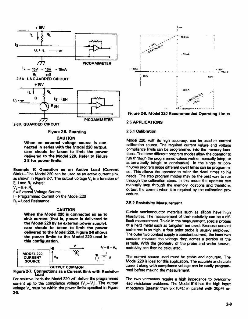
Example 8 Uslng Guard - Leakage resistance between low current conductors and nearby voltage sources can cause significant error currents. For example, If a printed circuit element has a leakage path with a resistance of 10% to a. nearby 15V supply terminal, a current of 15nA will be generated as shown in Figure 2-6a. In order to keep this current below 1 pA, the leakage resistance would have to be above 1.5 x 10%. This high resistance is difficult to maintain in many situations. In order to eliminate such stringent insulation resistance requirements, guarding techniques may be used as shown in Figure Z-6b. Guarding is surrounding the sensitive input with a conductor (the guard) connected to a low impedance point which is at (virtually) the same potential. The GUARD terminal located on the rear panel provides an easy connection to a low imped- ance voltage source which is equivalent to the output compli- ance voltage. The maximum load capacitance for the guard output is O.OluF. The maximum load current which includes guard and output is not to exceed 105mA. The accuracy of the guard +lmV excluding output lead I*R voltage drop.
Example 9 Floating Opsrstlon - The Model 220 can be floated off chassis ground. Guard or output common MUST NOT be connected to chassis ground when floating the instru- ment above chassis ground potential. Chassis ground is con- nected to earth ground with the line power cord and an appropriate grounded three-wire receptacle. The Model 220 can be floated up to 250Vrms above chassis ground.
TRlGGER MOOEL 220 REAR PANEL
Flgurs 2-5. Using the Model 220 External Trlggsr
2-8
+ 15v
‘S
b+IL - I I 1 J PICOAMMETER
‘L = 15V = 16V =15nA s;;ro4
2.6A. UNGUARDED CIRCUIT +15v
)RL I I
1 I I I PICOAMMETER
2-66. GUARDED CIRCUIT
Figure 2-B. Guarding
CAUTION When en external voltage source is con- nected in series with the Model 220 output, cere should be taken to limit the power delivered to the Model 220. Refer to Figure 2-B for power limits.
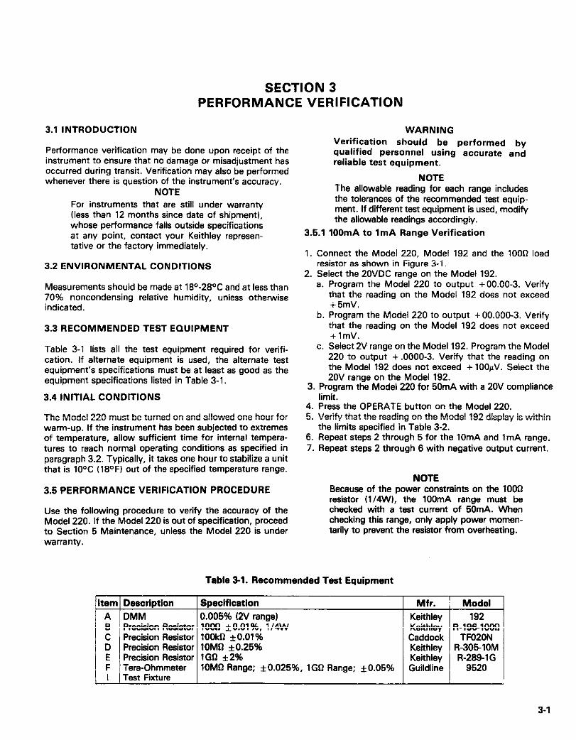
Example 10 Operation as en Active Loed (Current Sinkl-The Model 220 can be used as an active current sink as shown in Figure 2-7. The output voltage V, is a function cf E, I and R, where: V,=E+IR, E= External Voltage Source I = Programmed Current on the Model 220 R,= Load Resistance
CAUTION When the Model 220 is connected so es to sink current (that is, power is delivered to the Model 220 by en external power supplyl, cere should be taken to limit the power delivered to the Model 220. Figure 2-B shows the power limits to the Model 220 used in this oonfigumlon.
p$iiq~~~T
Figure 2-7. Fordeotions es 8 Current Sink with Resistive
For resistive loads ths Model 220 will deliver the programmed current up to the compliance voltage iV,=VJ. The output voltage V, must be within the power limits specified in Figure 2-B.
L k- ,Oorn/\ .-__-_ ----!
Figure 2-B. Model 220 Recommended Operating Limits
2.5 APPLICATIONS
2.5.1 Calibration
Model 220, with its high accuracy, can be used as current calibration source. The required current valuss and voltage compliance limits can bs programmed into the memory loca- tions. The three diismnt program modes allow the operator to run through ths programmed values wether manually (step) or automatically (single or continuous). In the single or con- tinuous program mode different dwell times can be programm- ed. This allows the operator to tailor the dwell times to his needs. The step program modes may be the best way to run through the calibration steps. In this mode the operator can manually step through the memory locations and therefore, output the current when it is required by the calibration pro- cedure.
2.5.2 Resistivity Measurement
Certain semiconductor materials such as silicon have high resistivities. The measurement of their reslstivity can be a dif- ficult measurement. To aid in the measurement, special probes of a hard metal such as tungsten are used. Because contact resistance is so high, a four point probe is usually employed. The outer two contact supply a constant current, the inner two contacts measure the voltage drop across a portion of the sample. Wti the geometry of the probe and wafer known, resisdvity can then bs calculated.
The current source ussd must be stable and accurate. The Model 220 is ideal for this application. The accurate and stable current along with compliance voltage can bs easily progmm- med before making the measurement.
The two voltmeters require a hiih impedance to ovemome laad resistance problems. The Model 614 has the high input impedance (greater than 5 x 1OpO in parallel with 2OpFl re-
2-9

quirad to make the measurement accurately. Refer to Figure 2-9.
For most wafers the resistivity is calculated from: P = kty k isa constant based on the geometn/ of the wafer and probe. t is the sample thickness. V is the meesurad voltage. I is the current in the sample.
Figure 2-10. Diode Chsradterization
Figure 2-9. Resistivity Measurement Using the Model 220 and Model 614
2.5.3 Diode Characterization
With the Model 220 it is possible to plot I-V (current-voltage) characteristics of a diode over several decades. Figure 2-10 shows the configuration to be used. The Model 614, with its high input resistance in the volts function; will allow the measurement to be made accurately. Figure 2-11 shows several examples of diodes whose curves have been plotted using the configuration of Figure 2-10.
I I I 1
.I .2 .3 .a 5 5 “F
Figure 2-11. Diode Curves
2-10
SECTION 3 PERFORMANCE VERIFICATION
3.1 INTRODUCTION
Performance verification may be done upon receipt of the instrument to ensure that no damage or misadjustment has occurred during transit. Verification may also be performed whenever there is question of the instrument’s accuracy.
NOTE For instruments that are still under warranty (less then 12 months since date of shipment), whose performance fells outside specifications et any point, contact your Keithley represen- tative or the factory immediately.
3.2 ENVIRONMENTAL CONDITIONS
Measurements should be made et lE”-28OC and et less than 70% noncondensing relative humidity, unless otherwise indicated.
3.3 RECOMMENDED TEST EQUIPMENT
Table 3-l lists all the test equipment required for verifi- cation. If alternate equipment is used, the alternate test equipment’s specifications must be et least es good as the equipment specifications listed in Table 3-l.
3.4 INITIAL CONDITIONS
The Model 220 must be turned on end allowed one hour for warm-up. If the instrument has been subjected to extremes of temperature, allow sufficient time for internal tempera- tures to reach normal operating conditions es specified in paragraph 3.2. Typically, it takes one hour to stabilize a unit that is 10°C (18OFl out of the specified temperature range.
3.5 PERFORMANCE VERIFICATION PROCEDURE
Use the following procedure to verify the accuracy of the Model 220. If the Model 220 is out of specification, proceed to Section 5 Maintenance, unless the Model 220 is under warranty.
WARNING Verification should be performed by qualified personnel using accurate and reliable test equipment.
NOTE The allowable reading for each range includes the tolerances of the recommended test equip- ment. If different test equipment is used, modify the allowable readings accordingly.
3.5.1 lOOmA to 1mA Range Verification
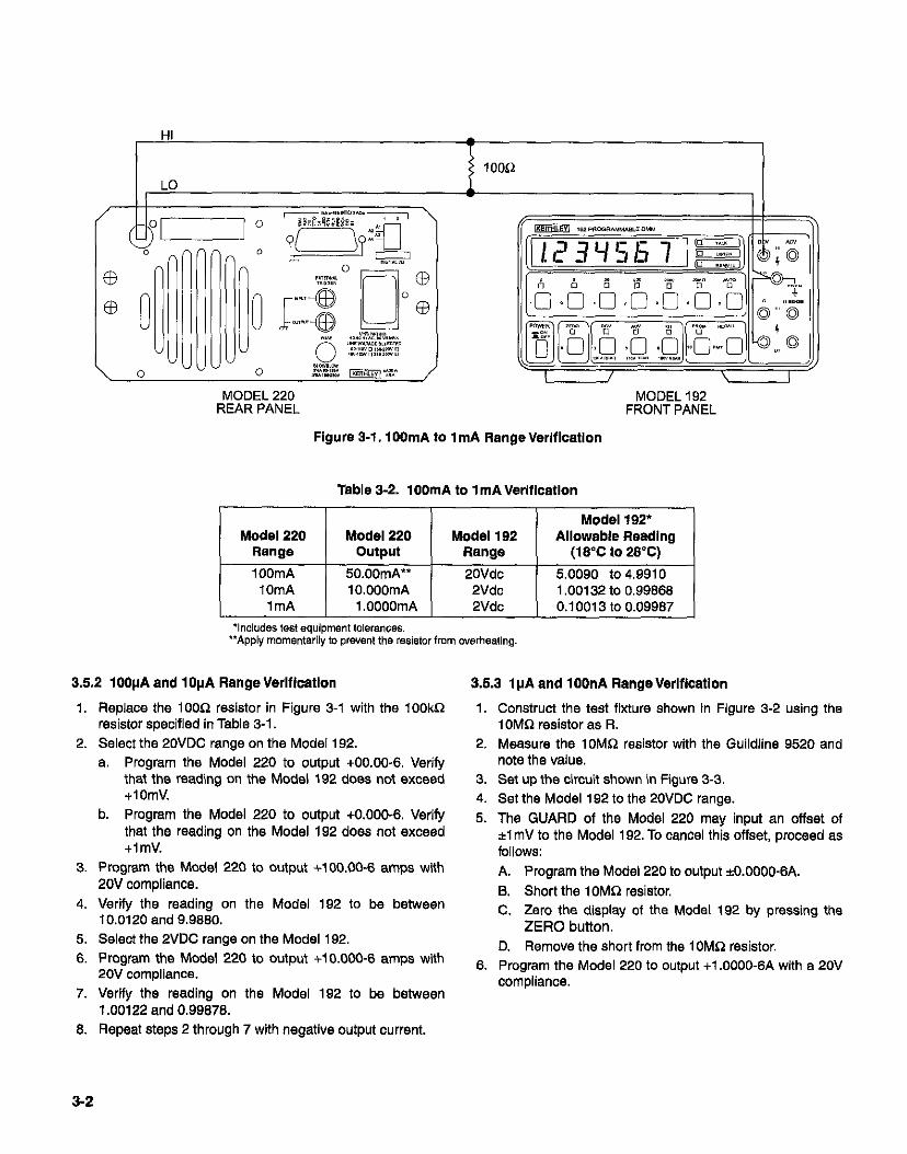
1. Connect the Model 220, Model 192 end the 1OOR load resistor as shown in Figure 3-1.
2. Select the 20VDC range on the Model 192. a. Program the Model 220 to output +OO.OO-3. Verify
that the reading on the Model 192 does not exceed + 5mV.
b. Program the Model 220 to output +OO.OOO-3. Verify that the reading on the Model 192 does not exceed +lmV.
c. Select 2V range on the Model 192. Program the Model 220 to output + .OOOO-3. Verify that the reading on the Model 192 does not exceed + 1OOAV. Select the 20V range on the Model 192.
3. Program the Model 220 for 50mA with a 20V compliance limit.
4. Press the OPERATE button on the Model 220. 5. Verify that the reading on the Model 192 display is within
the limits specified in Table 3-2. 6. Repeat steps 2 through 5 for the 1OmA end 1mA range. 7. Repeat steps 2 through 6 with negative output current.
NOTE Because of the power constraints on the 1OOD resistor f1/4W). the lOOmA rat-toe must be checked with a test current of 5timA. When checking this range, only apply power momen- tarily to prevent the resistor from overheating.
Table 3-l. Recommended Teat Equipment
Item/ Description Specification
A DMM 0.005% (2V range) B Precision Resistor 1OOB +O.Ol%. 114W C Precision Resistor lOOkg-*O.Ol % D Precision Resistor 1OMD f0.25% E Precision Resistor 1GD f2% F Tera-Ohmmeter 1OMD Range; iO.O25%, 1GD Range; f0.05%
i I Test Fixture I 3-1
MODEL 220 REAR PANEL
MODEL 192 FRONT PANEL
Figure 3-l. lOOmA to 1mA RangeVerifIcation
Table 3-2. 100mA to 1 mA Verlflcatlon
Model 192” Model 220 Model 220 Model 102 Allowable Readlng
Range output Range (16% to 28°C)
lOOmA 50.00mA” 2OVdC 5.0090 to 4.9910 IOmA lO.OOOmA 2Vdc 1.00132 to 0.99666
1mA 1 .OOOOmA 2Vdc 0.10013 to 0.09967
‘Includes test equipment l&mnc86. “Apply momentarily to prevent the resistOr from overheating.
3.5.2 lOOvA and 10vA RangeVerIficatIon
1. Replace the 1OOQ resistor in Figure 3-1 with the lOOka resistor specified in Table 3-1.
2. Select the 20VDC range on the Model 192. a. Program the Model 220 to output +OO.OO-6. Verify
that the reading on the Model 192 does not exceed +lOmV.
b. Program the Model 220 to output +O.OOO-6. Verify that the reading on the Model 192 does not exceed +ImV.
3. Program the Model 220 to output +100.00-6 amps with 20V compliance.
4. Verify the reading on the Model 192 to be between 10.0120 and 9.9660.
5. Select the 2VDC range on the Model 192. 6. Program the Model 220 to output +lO.OOO-6 amps with
20V compliance. 7. Verify the reading on the Model 192 to be between
1.00122 and 0.09676. 6. Repeat steps 2 through 7 with negative output current.
3.6.3 1 pA and 1 OOnA Range Verlflcatlon
1. Construct the test fixture shown in Figure 3-2 using the 1 OMfi resistor as R.
2. Measure the lOMa resistor with the Guildline 9520 and note the value.
3. Set up the circuit shown in Figure 3-3. 4. Set the Model 192 to the 20VDC range. 5. The GUARD of the Model 220 may input an offset of
*l mV to the Model 192. To cancel this offset, proceed as follows: A. Program the Model 220 to output *O.OOOO-6A. i3. Short the 1 OMQ resistor. C. Zero the display of the Modal 192 by pressing the
ZERO button. D. Remove the short from the 10Mn rssistor.
6. Program the Model 220 to output +l.OOOO-6A with a 20V compliance.
3-2

7. Using the measured value of the 1OMR resistor, calculate the voltage drop ecross that resistor. Example: f + 1 .OOOO-6A) x llO.OOlMQ) = lO.OOlOV. IModel 220 Programmed Output1 x (Measured Resistance) = (Expected Voltage Drop Across RI.
8. Verii that the reading on the Model 192 is the calculated voltage drop f0.0165V.
9. Place the Model 220 in the standby mode and take the Model 192 out of the zero mode (ZERO annunciator off).
10. Set the Model 192 to the 2VDC range. 11. Cancel the effects of guard offset from the Model 220 as
follows: A. Program the Model 220 to output +OOO.O-9A. B. Short the 10MQ resistor. C. Zero the display of the Model 192 by pressing the
ZERO button. D. Remove the short from the 1OMD rasistor.
12. Program the Model 220 to output + lOO.O&9A with a 20V compliance.
13. Using the measured value of the 1OMB resistor, calculate the voltage drop across that resistor. Example: f+ lOO.OO-9A) x (lO.OOlMD) = l.OOOlOV. (Model 220 Programmed Output) x (Measured Resistance) = (Expected Voltage Drop Across RI.
14. Verify that the reading on the Model 192 is the calculated voltage drop *O.O0367V.
15. Repeat steps 4 through 14 with negative current output 16. Place the Model 220 in the standby mode and take the
Model 192 out of the zero mode
r--------i
1. To decrease settling times and to assure accurate calibrations. it is recommended to use an internal guard Ias shown in the drawing aboveI. The guard mwf be insulated from the surrounding case.
2. To further minimize inaccuracies. current leakage paths to ground for guardl mwst be minimized. This requires the use of low leakage insu- Ming materials for conStruction and the use of special cleansing agents such as freona to clean the components and insulators after construe- don.
Figure 3-2. Test Fixture
3.6.4 1OnA and 1nA Range Verification
1. Construct the test fixture shown in Figure 3-2 using the 1GD resistor specified in Table 3-l.
2. Measure the 1GR resistor with the Guildline 9520 and note the value.
3. Set up the circuit shown in Figure 3-3. 4. Set the Model 192 to the 20VDC range. 5. Cancel the effects of guard offset from the Model 220 as
follows: A. Program the Model 220 to output O.OOO-9A. B. Short the 1Gfl resistor. C. Zero the display of the Model 192 by pressing the
ZERO button. D. Remove the short from the IGQ resistor.
6. Program the Model 220 to output C lO.OOO-9A with a 20V compliance.
7. Using the measured value of the 1GD rssistor, calculate the voltage drop across that resistor. Example: f + 10.0009A) x fl.OOlGfB = lO.OlOOV. (Model 220 Programmed Output) x (Measured Resistance) = (Expected Voltage Drop Across R).
8. Verii that the reading on the Model 192 is the calculated voltage drop *O.O34OV.
9. Place the Model 220 in the standby mode end take the Model 192 out of the zero mode.
10. Set the Model 192 to the 2VDC range. 11. Cancel the effects of guard offset from the Model 220 as
follows: A. Program the Model 220 to output + .OOOO-9A. B. Short the 1GQ resistor. C. Zero the display of the Model 192 by pressing the
ZERO button. D. Remove the short from the 1GR resistor.
12. Program the Model 220 to output + 1 .OOOO-9A with a 20V compliance.
13. Using the Measured value of the 1GD resistor, calculate the voltage drop across that resistor. Example: f + 1.00069A) x fl.OOlGD) = .OOlOOV. (Model 220 Programmed Output) x (Measured Resistance) = fExpsctad Voltage Drop Across RI.
14. Verify that the reading on the Model 192 is the calculated voltage drop *0.00542\1.
15. Repeat steps 4 through 14 with negative current output.
Figure 3-3. lpA-1nA Range Verification
3-313-4

SECTION 4 THEORY OF OPERATION
4.1 INTRODUCTION
This section contains circuit descriptions for the Model 220. The information is arranged to provide a circuit description of individual functional circuit blocks. To facilitate understanding, the descriptions are keyed to accompany simplified block diagrams and schematics. Detailed schematics of the Model 220 are located in Section 6.
4.2 BLOCK DIAGRAMS
The circuitry of the Model 220 is represented by the two simplified block diagrams in Figures 4-l and 4-2. Figure 4-1 shows a simplified block diagram of the Model 220’s analog circuitry (power supply, range circuitn/, amplifiers etc.). Figure 4-2 shows a simplified block diagram of the Model 220’s digital circuitry (microprocessor, RAM, ROM, VIA etc.).
4.3 POWER SUPPLY
To facilitate understanding of the following discussion refer to schematic diagram 220-106 (sheet 2 of 21. The power supply is a conventional AC to DC power converter. Trans- former TlOl, has three separate secondaries that are fed in- to three separate bridge rectifiers CRlOl, CR108 and the bridge configuration of CR102 through CR105. The output of CR101 is fed into regulator VRlOl and is filtered by Cl07 and Cl03 producing the +5V digital supply. The output of CR108 is fed into VR102 and VR103 and is filtered by Cl19 through Cl22 to produce the positive and negative 15V sup- plies. The output of CR102 through CR105 is filtered by Cl17 and Cl18 to produce the positive and negative 125V supplies. R118 and R119 are bleeder resistors to prevent charge retention after AC power is removed.
A tap off of the primary of the transformer TlOl supplies the nominal 115VAC to the fan.
4.4 ANALOG BOARD
To facilitate understanding of the following discussion refer to schematic diagram 220-128 (sheet 1 and 2).
The heart of the analog board is the high voltage electro- meter op amp which is centered on U319. The performance of U319 is bootstrapped up to the voltage levels supplying 0318 and Q319 bY Q315-Q319, 0313-0318 and their associated circuitry. 0301, 0302, R344, R348, R349, C313 and C320 establish frequency stability for U319. R343 is an input voltage offset adjustment for U319.
A constant current source can be derived by a series voltage source and resistance from the output (analog com- monlguardl to the amplifier input. The amplifier input to the common of the high voltage supplies of Q318/Q319 (output common) comprises a current source. Range resistors R358, R361. R362. R378, R375, R376, R380 and R381 along with their associated calibration potentiometers, com- prise the series resistance section of the current source. These resistances connect to the input node of the amplifier through relays K301-K305. When several resistances are connected through a common relay, JFET switches 0303 through Q310 are used to distinguish which resistor is being used. Several JFETs are organized in pairs for voltage sen- sing at the resistor to compensate for the voltage drop in the current carrying JFET.
U315 serves as a sense amplifier with Q311, Q312, R344 and R345 as a high current buffer for the higher current ranges. U314, U318A and U320 8, C, D, E and F drive the range relays. U3188, U317 and U313 A, 8, C and D drive the JFET switches. U313 and U317 are voltage comparators with open collector outputs, Cbmbined with R350, this circuitry provides the voltage drive for the switching JFETs.
The voltage source section centers around U311, the 12 bit digital to analog converter (DACI. Associated circuitry R301 through R307 and R316, are used to adjust offset and positive gain. Gain is set on the 1mA range and therefore R376 does not have an adjustment. Following this circuitry is a n?twork providing a +/- operator to the output of U311. U312 provides the active portion while switches on U306 along with resistors R317, R318, R320 and R323 pro- vide a selectable gain of + 1 or -1.
R318 provides a gain adjust f-1mAl for this operator. The output is fed to the sense amplifier U315. R392 is an offset voltage adjustment potentiometer for U312 and U315.
Serial to parallel shift/store registers U301, U302 and U303 provide digital control from the serial data link. Data is input- ted via the clock and latch lines. Latch selects the data in mode as either recirculated data out flatch=logic 01 or the overcompliance (V-limit) information (latch = logic 1). This selection is performed by U304A and 8, U3168 and C and U305A.
Gates U3058, C and D form a flip-flop for controlling the tri- state mode of the outputs of U301, U302 and U303. This circuitry, along with R351, R352, CR307, C305, etc., prevents erroneous current source outputs both on acquisi- tion and loss of AC line power.
4-1

DIG
ITAL
C
ON
TRO
L
> n
1 ‘-I_
OU
TPU
T
ITR
IAXI
AL
REC
EPTA
CLE
]
:
POW
ER
SUPP
LY
+ i!!!?
? EL
ECTR
OM
ETER
O
P.AM
P
-JC
L<
GU
ARD
I O
UTP
UT
CO
MM
ON
CH
ASSI
S G
RO
UN
D
Figu
re
4-1.
Ana
log
Circ
uitry
B
lock
D
iagr
am
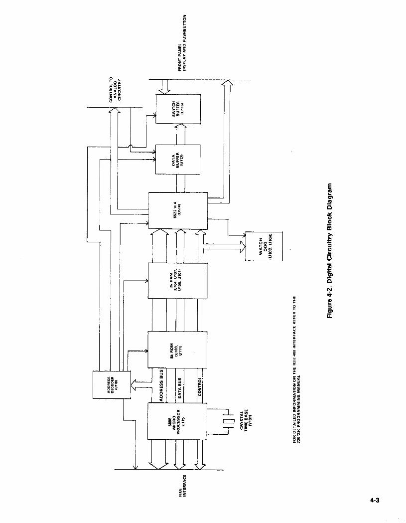
Figu
re
4-2.
Dig
ital
Circ
uitry
B
lock
D
iagr
am
The remaining portion of the analog circuitry produces the selectable compliance voltage limit. An 8 bit digital-to- analog converter (DACl U308 starts this process. With 128 combinations, each step is scaled to represent one volt of compliance. Since U308 is a current output DAC, U309 is required to revert back to a voltage level. The output of U309 then represents the selected compliance voltage scaled down by a factor of 20.
This signal and its inverse fU309A. R324 and R327l are applied to divider network R331 and R336 which are refer- enced to output common, At the junction of each divider network is an amplifier which reverses the previous scaling factor. Resulting from this is an error voltage approximately equal to the difference between the actual compliance volt- age level and the programmed level. Each amplifier U307A and B and the associated circuitry, is coupled through diodes CR303 and CR302 on R333. The polarity of the diodes is arranged such that a voltage is impressed on R333 only when the actual voltage compliance exceeds + i- the programmed value. This result is applied to the output node via low leakage diode CR304 preventing any further com- pliance voltage excursion. Current from the range resistors is shunted through diodes CR305 end CR306 when this operation limit occurs. Resistors R330 and R332 add an off- set to compensate for diode drops in CR302 through CR304.
The circuit configuration of U313A and B comprise a win- dow comparator to detect a V-limit condition across R333. The comparator limits are set by resistor divider network R338 through R341. U313A and B open collector outputs are configured in a “wire ORed” fashion through pull up resistor R346. Whenever the voltage across R333 exceeds the comparator limits, a logic 1 is developed through current limiting resistor R347 to the output of inverter U316E. C311 is used for stabilization.
VR301 supplies the digital circuitry with the required + 5V. This voltage is also supplied to the digital board for use by the ooticallv isolated portion of the circuitry.
4.5 DIGITAL BOARD (Microcomputer)
To facilitate understanding of the following discussion refer to schematic diagram 220-106 (sheet I of 2). For an overall block diagram of the digital circuitry refer to Figure 4-2.
The microcomputer and its associated logic circuitry, con- trols front panel functions (source, dwell time, program control etc.), operation of the front panel display and data through the IEEE-488 interface circuitry.
dress lines A13, Al4 and A15; UllO sections the 64k of memory space into 8k end 4k segments. The total memory used is a small portion of the entire addressing capabilities of the 6808 microprocessor U115. Memory locations for the 64k addresses are assigned the values 0000,s through FFFF,,.
Interfacing of the microprocessor with the RAMS. ROMs. Front Panel, VIA or the IEEE-488 interface is controlled by the address decoder, UI IO.
Partial address decoding is used in this system. The function selected is determined by the state of the address lines A13, AI4 and A15. These address lines determine which output is selected at the decoder UlIO in accordance with the memory map. Only one of the devices (RAM, ROM, VIA, etc.1 will have access to the data bus at any time. The ed- dress decoder selects one of the devices only after a Valid Memon/ Address VMA has been asserted et the decoders input EN (pin 61. The VMA signal is generated by the 6808 microprocessor.
Timing for the computing sequence is provided by the 4MHz crystal YlOl. The 6808 microprocessor divides this signal by four to produce a 1MHz signal at the a2 output (pin 37).
U102, U104, UlOK, U108C and their associated circuitry, forms a reset network (watchdog) which resets the micro- processor, VIA and the IEEE-488 interface. The circuit actuates in the event the front panel display is not updated after a specific period of time has elapsed due to a lost pro- gram or power line transient.
The digital circuitry is optically isolated from the analog cir- cuitry by AT101 through AT104, U113A, B, U117 and their associated circuitry. The output signals consist of latch, clock and data out. These signal lines permit serial com- munication to the analog circuitn/. The data in signal line is received from the analog circuitry and is either the recircu- lated data or the overcompliance (V-limit) data depending on the state of the latch line. When the latch line is a logic 1, the data in line will represent the compliance state (logic 1 implies an overcompliance or V-limit). When the latch line is a logic 0. the data in line will be the recirculated data sent out to the analog side as data out. This data is inverted on the digital side of the isolation.
The remaining circuitry on the digital board consists of ex- ternal trigger inputs and outputs. C123, CRI12, CRlIl, R121 and R128 comprise an input protection network for trioaerino inout to PB6 of the VIA KJI14l. VlI3D. CR109.
The microcomputer includes a 6808 microprocessing unit CRilO, 6127 and R122 buffer a triggered output originated
UI15; a 6522 versatile interface adapter UI14; two 2732 on PB3 of the VIA fU114l.
ROMs U109 and Ulll; four 2114 RAMS UlOl, U103, U105 4.6 DISPLAY ClRCUlT and U107; an address decoder UllO: a data busdriverU116 end the necessary reset logic. The memory utilized in this system is shown in the memory map (Figure 4-3). Using ad-
The display information is outputted on PA0 through PA7 on the VIA 11/O) bus. The information is updated at a 1kHz
44
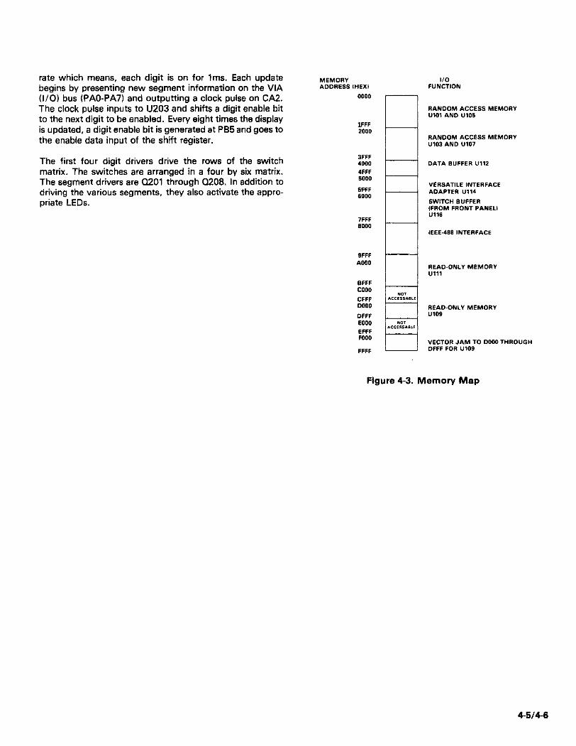
rate which means, each digit is on for lms. Each update begins by presenting new segment information on the VIA (I/O) bus (PAO-PA7) end outputting a clock pulse on CA2. The clock pulse inputs to U203 and shifts a digit enable bit to the next digit to be enabled. Every eight times the display is updated, a digit enable bit is generated at PB5 and goes to the enable data input of the shift register.
The first four digit drivers drive the rows of the switch matrix. The switches are arranged in a four by six matrix. The segment drivers are D201 through D208. In addition to driving the various segments, they also activate the appro- priate LEDs.
MEMORY ADDRESS l”EX,
woo
Figure 4-3. Memory Map
4-514-6

SECTION 5 MAINTENANCE
5.1 INTRODUCTION
This section contains information necessary to maintain the Model 220. Calibration adjustment, troubleshooting, fuse replacement, line voltage selection, fan filter cleaning and all information pertinent to maintenance is provided.
5.2 CALIBRATION
Calibration should be performed yearly (every 12 months.1 or whenever performance verification (see Section 3) indicates that the Model 220 is out of specification. If any step in the calibration procedure cannot be performed properly, refer to paragraph 5.4 for troubleshooting information or contact your Keithley representative or the factory.
WARNING All service information is intended for qualified electronic maintenance person- nel only.
5.2.1 Recommended Test Equipment
Recommended test equipment for calibration is listed in Table 5-1. Alternate test equipment may be used. However, the accuracy of the alternate test equipment must at least be equal to the specifications in Table 5-I.
5.2.2 Environmental Conditions
Calibration should be performed under laboratory condi- tions having an ambient temperature of 23°C f I°C and a relative humidity of less than 50%.
5.2.3 Warm-Up
The Model 220 must be turned on and allowed one hour for warm-up. If the instrument has been subjected to extremes of temperature, allow sufficient time for internal tempera- tures to reach normal operating conditions. Typically, it takes one hour to stabilize a unit that is IO°C 118°F) out of the specified temperature range.
5.2.4 Calibration Fixtures
In order to meet the specifications of the Model 220, the IOMDand 1GIl resistors used to calibrate the Model 220 must be enclosed in a guarded fixture. The guarded fixture must be constructed. The following items are necessary for proper construction of the calibration fixture: I. 1OMR Resistor, Keithley Part Number R-305-10M 2. IGQ Resistor, Keithley Part Number R-289-1G 3. Two enclosed chassis boxes, one to be placed inside the
other and insulated from each other. 4. One Triax Connector, Keithley Part Number CS-181 5. One Banana Jack, Keithley Part Number BJ-II
The test fixture shown in Figure 5-2 is to be used to calibrate the 1fiA and lOOnA ranges. A duplicate test fixture must be constructed with the 1GTi resistor in order to calibrate the 1OnA and InA ranges.
Figure 5-l. Calibration Setup
Table 5-l Recommended Test Equipment
Item
A
: D E F
: I
Description
DMM Resistor” Resistor* Resistor* Resistor* Resistor* Resistor*
Teraohmeter Calibration Fixture
Specification
f0.00596 to lo& 100 k.l%
loon f .l% IkD f .l%
1OOkfl + .02% IOMD f .25%
1GD ~2%
NOTE* . Before placing the resistors in the test configurations, measure them and note the value. Zero the Model 192 before measuring the 100, lOOR, 1kD and the 1OOkR resistors with the Model 192. Measure the 1OMD and 1GD resistors with the Guildline 9520. These values will be used later in the calibration procedure.
Mfr. Keithley Keithley Keithlev Keithley Keithley Keithlev Keithlev Guildline
Model 192
R-185-10 R-308-1003 R-315-1 k R-182s100k R-305~10M R-289-I G
9520
5-1

5.2.5 Calibration Adjustments
Use the following procedure end make the adjustments in- dicated to calibrate the Model 220. To locate adjunment points, remove the top cover and refer to the analog board shield.
WARNING To prevent a shock hazard, turn the instru- ment off, remove the line cord and all test leads from the instrument before remov- ing the top cover.
1. Remove the top cover (see paragraph 5.5, step II. Werm- up with top cover in place. Minimize the time the cover is removed.
2. Short the output of the Model 220 (HI to LO). Monitor the guard output with the Model 192 (Item A Table 5-l) on the .2VOC range. Program the Model 220 for an out- put of + .OOOO-3 amps and a compliance of IOV. Locate and adjust R343 for a reading on the Model 192 of .oooooo f 20/&v.
3. Remove the short from the output and connect the Model 220 and Model 192 as shown in Figure 5-1. Pro- gram the Model 220 output +.OOOO-3 amps. Monitor the Model 220 output on the Model 192. Invert the Modal 220 output (press + and ENTER on the Model 220) and note the change in current. Calculate the average reading when the output is changed from positive to negative and adjust R304 for the calculated value. Then adjust R392 for a reading of less than
5. Remove the current measurement test configuration and monitor the Model 220 output with the Model 192 on the 200VDC range. Program the Model 220 to + 19,OOOE-6 amps and a compliance of 1OOV. Adjust R319 for a reading of 100.000 f 0.2V.
6. This completes the calibration of the Model 220. To verify correct calibration refer to Section 3.
r--------i I - I
Construction Noms: 1. TO decrease settling times and 10 assure accurafe calibmtions. it is
recommended to “se an internal guard Ias show” in d,e drawing abovel. The guard must be insulated from the wrraunding case.
2. To futihe, minimize inaccumcies, current leakage paths to ground IO, guardl must be minimized. This requires the use of low leakage insu- lath9 materials for construction and the use of special cleansing agents such as freona to clean the components and insulators after consl,uc- lion.
Figure 52. Calibration Fixture
f IOOnA ClOO$J across 1kG). I I 4. Set up the circuit shown in Figure 5-1 and 5-3. Follow Table Figure 53. IpA to InA Calibration
5-2 to calibrate the ranges of the Model 220. 5.3 FUSE REPLACEMENT NOTE
The allowable reading on the Model 192 is the product of the measured shunt resistance times
If power fails, first verify that the fuse ( FlOl ) is not defective
the Model 220 output. For example in Table before disassembling the Modal 220. If the line voltage set-
5-2, step a: ting is changed IS1021 the fuse must be replaced according
measured shunt resistance = IkQ to Tables 6-3 and 6-4. The fuse is accessible from the rear
Model 220 output = 1.9mA panel. To replace the fuse proceed as follows:
calculated output = 1.9V f 300ppm or 570~1V 1. Turn power off and disconnect the line cord.
-
E?!
E
: e f
Lf 0
L l 1
-1
6-2
-I- 120 Eettlng
IRange) 1 .SE-3 -1.8E-3 looE-3 19E-3
WOE-6 19E-8
1.9E-6’ WOE-9’ 19~9”” 1 .SE-p*
( :ompliince 3OV 3ov 3ov 3ov 3ov
L 3OV
30V
:: 3OV
I ms cansbucted 1OMGGua I ths constucted 1GG Gual
Table 5-2. Calibration
idjustment 1 Shunt 1 Model 192 1 Allowable Reading on the Model 192 at 6% Digit Point 1 R 1 Range lResdutfon R303 1 1kG 1 2VDC 1 (lkG)(l .SE-3) = Calculated Output i3Ogpprn or 57OuV I.7318 1kS-I 2VDC (lkWl.SE-3) = Calculated Ou+ut **pm or 57&/ R38l I?386 i%I
2VDC 1lOG~WWE-3l= Calculatsd Output *76@pm or 76OpV 2VDC WlOG1~18&3~= Calculated Output *3O@pm or 670#
R386 1OW-l 20VDC KUNdIWOEB)=Calurlatad Output &2Wppm or 4.8mV R384 lOWI 2VDC 11OWGWE-6~ = Calculated Output f3Wppm or 67OfiV
IShunt Measurement Technique1 I User of Guarded Fochrasl
kzi 10MG 20VDC (lOMG)(l.8E-6)=Calculatsd Output H9Oppm or 11.4mV 1OMi-l 2VDC fl0MG)(18E-8j=Calculatad Output *woqYnn or 4.76m\
zig 1GG 20VDC (lGlW19E-9) = Calculatad Output f226@pm or 42.8mV IGO 2VDC ~lG~)l1.8E-9)=Calcuiatad Output f225@pm or 4.28mV
xi F&m in tha circuit shown in Faum 6-3. d Fnbre in ths circuit shown in Figure 53.

2. The fuse carrier is spring loaded. Using a slotted screw- driver, push the fuse carrier in and rotate K-turn counter- clockwise. The carrier and fuse will eject from the holder.
3. Remove the fuse from the carrier and replace per Table 5-3 or Table 5-4.
WARNING To prevent a shock hazard, always turn the instrument off and disconnect the line cord before replacing the line fuse.
CAUTION Do not install a fuse with a higher rating than specified in Table 5-3 or 5-4. Instru- ment damage may result.
4. To install the fuse and carrier into the holder, reverse the procedure in step 2.
Table 5-3. Fuse Replacement, 3AG Sire
Line Fuse FlOl Keithley Voltage Pert No.
9OV-11OV” 3/4A, 25OV. 3AG. SLO BLO FU-19 105V-125V 3/4A. 250V. 3AG. SLO BLO FU-19 18OV-22OV* 3/8A, 250V; 3AG; SLO BLO FU-18 ZlOV-250V 3/8A, 25OV, 3AG. SLO BLO FU-18
“Requires special factory installed transformer TR-187.
Table 5-4. Fuse Replacement, 5mm Size
Line Fuse FlOl Keithley Voltage Part No.
9OV-llOV* 0.8A. 25OV, SLO 8LO FU-52 105V-125V 0.8A, 250V. SLO BLO FU-52 18OV22OV’ 0.4A. 25OV. SLO BLO FU-53 ZlOV-250V 0.4A. 25OV. SLO BLO FU-53
*Requires special factory installed transformer TR-187.
5.4 LINE VOLTAGE SELECTION
Set up the Model 220 to operate on the available AC line voltage as follows:
WARNING To prevent a shock hazard, turn the instru- ment off and disconnect the line cord. Also, remove all test leads from the instru- ment before removing the top cover.
1. Remove the top cover (see paragraph 5.5 step 11. 2. Refer to Table 55 and set switch S102 (located near the
transformer, underneath the IEEE488 interface board) accordingly.
3. Install proper fuse per paragraph 5.3. NOTE
The line voltage setting of the instrument is marked on the rear panel. The following pro- cedure can be used either to confirm the fac- tory setting, or to set up the instrument for operating on another voltage range. If the line
voltage range is changed, the box next to the selected line voltage should be appropriately marked as an external reminder of the sening. Use a water soluble marking pen.
Table 5-5. Line Voltage Selection
~
*Requires special factory installed transformer TR-187.
5.5 DISASSEMBLY
If it is necessary to remove or replace a component, use the following procedure to aid in disassembly of the Model 220.
1. Remove the top cover as follows:
WARNING Turn the instrument off, remove all test leads from the instrument and disconnect the power cord before removing the top CO”W.
a. Remove the two retaining screws located at the rear of the instrument.
b. Grasping the top cover at the rear, carefully lift it off the instrument.
c. When installing the top cover, make sure that the three tabs located at the front of the cover engage in the front panel assembly.
2. Remove the IEEE-488 interface board. a. Unplug ribbon cable (J/P1004) at the mother board. b. Remove the phillips head retaining screw located near
J1004 on the interface board. c. Remove the two retaining bolts that secure the inter-
face board and IEEE-488 connector to the rear panel. d. Lift the interface board out of the mainframe.
3. Remove the analog board shield. a. Remove the four slot head screws that secure the
shield to the analog board. b. Lift the shield and the four slot head screws away from
the analog board. 4. Remove the input node and relay analog shields.
a. Remove the single phillips head screw located in the middle of the shield.
b. Lift both shields away from the analog board.
NOTE The circuitry located beneath the analog board shields is extremely sensitive. Do not touch any of the range resistors or input cable.
5. Remove the analog board. a. Remove the phillips head screw located directly behind
the two power transistors with heat sinks.
5-3

b. Unplug the ribbon cable (J/P10031 from the analog board.
c. Remove the bonom shield of the analog board by removing the two phillips head screws that secure the shield to the board.
NOTE Do not remove the input cable.
6. Place the analog board along the side of the Model 220. 7. Remove the mother board from the case.
a. Remove the four plastic standoffs. b. Remove the two phillips head screws that secure the
mother board to the case. They are located at the rear of the mother board one by the fan and the other is by the line voltage selector switch S102.
c. Remove the two phillips head screws that secure the case to the rear panel.
d. Unplug the display ribbon cable fJ/PlOOZ) from the mother board.
e. Grasp the mother board and the rear panel simultaneously. Lift the mother board and rear panel up and toward the rear of the instrument. Then lift the mother board and rear panel out of the case.
8. Remove the display board. a. Remove the two phillips head screws that secure the
display board to the front panel. b. Remove the front panel bunons. c. Lift the display board out of the case.
9. For reassembly, perform steps 1-8 in reverse order.
NOTE When installing connectors J/P1004, J/P1003 and J/P1002 be sure to align pin one of the connector to pin one of the cable.
5.6 FAN FILTER MAINTENANCE
The internal temperature generated by the Model 220 necessitates the forced air cooling provided by the fan. The fan has an sir filter which keeps the Model 220 relatively free of dust and dirt. Dust and dirt collect on the filter and im- pede the air flow through the instrument. Lack of air flow will cause overheating. Therefore, the filter must be kept clean in order for the Model 220 to achieve optimum perfor- mance. To clean the filter: 1. Remove the filter from the fan. 2. Use compressed air to remove the dust and dirt from the
filter. If the filter is excessively dirty wash it in mild soap and water and dry it with compressed air.
3. Reinstall the filter.
5.7 SPECIAL HANDLING OF STATIC SENSITIVE DEVICES
MOS devices are designed to function at high impedance levels. Normal static charge can destroy these devices. Table 5-6 lists all the static sensitive devices of the Model 220. Steps 1 through 7 provide instruction on how to avoid damaging these devices.
5-4
Table 5-6. Model 220 Static Sensitive Devices
Reference Designation
UlOl, u103. u105, u107 u102 u109 Ulll U112, U301, U302, U303 u114 u115 U116 u304 u305, u314 U306 U308 u311 U316 MO2
Leithley Part No.
LSI-15 IC-197
220-800-85 220-801-85
IC-251 LSI-28 LSI-27 IC-250 IC-138 IC-102 IC-320 IC-321 IC-323 IC-106 TG-139
1. Devices should be handled and transported in protective containers, antistatic tubes or conductive foam.
2. Use a properly grounded work bench and a grounding wriststrap.
3. Handle devices by the body only. 4. PC boards must be grounded to bench while inserting
devices. 5. Use antistatic solder suckers. 6. Use grounded tip soldering irons. 7. After devices are soldered or inserted into sockets they
are protected and normal handling can resume.
5.8 TROUBLESHOOTING
The troubleshooting information in this section is intended for use by qualified personnel who have a basic understand- ing of the analog and digital circuitry used in a precision test instrument. Instructions have been written to assist in isolating the defective circuit. Isolating the defective com- ponent has been left up to the troubleshooter. Refer to Table 5-7 for power supply checks. Refer to Table 5-8 for Analog board checks. Refer to Table 59 for digital circuitv checks. Refer to Table 5-10 for display board checks. Refer to Table 5-11. for IEEE-488 interface board checks.
NOTE For instruments that are still under warranty (less than 12 months since date of shipment), whose performance falls outside specification at any point, contact your Keithley represen- tative or the factory before attempting troubleshooting or repair.
5.8.1 Servicing High Impedance Circuitry
High impedance circuitry is extremely sensitive and must be kept clean of oil, dirt, dust and contaminants. Replacing a component or components within a high impedance circuit requires special cleaning and handling to maintain the high impedance level of the circuit. After replacing any compo-

nent in the high impedance circuitry, or if the high impe- dance circuitry (InA-1rA range resistors) are contaminated, use the following procedure to clean the circuit: 1. Clean the entire high impedance circuit with methanol
and a clean cotton swab. 2. Blow dry the circuit with dry nitrogen gas. 3. Inspect the circuit for any residue fcontamination) and
repeat steps 1 and 2 if any residue is found. 4. Reassemble taking care not to touch the clean com-
220 will display an errrx message corresponding to the defective chip. For example; the digital self test reveals that RAM chip number four is defective. The Model 220 displays a flashing:
jl
This informs the operator the RAM chip number four is defective. Refer to Figure 5-4 for chip number assignment.
5.8.2 Digital Self Test
Upon power-up the Model 220 performs a digital self test of the RAM (2114’s) chips and a cyclic redundancy check (CRC) of the ROM (2732’s) chips. If the self test or the CRC reveals a problem with any of the memory chips, the Model
a319 Collector Q318 Collector
Figure 5-4. Memory Chip Number Assignment
-
-
Table 5-7. Power SUpply Checks
Required Condition Unit turned on, properly rated FlOl has continuity. Line selector switch S102 verified in correct position. + 130VDC f 15% - 130VDC f 15% +15VDC+15% -15VDC?15% +5VDC+5%
Remarks
+ 125 Volt Supply” - 125 Volt Supply’ + 15 Volt Supply”” - 15 Volt Supply** + 5 Volt Digital Supply’“*
I I I *Referenced to output common. ‘i)
“Referenced to analog common. * ‘*‘Referenced to digital common. $
5-5

Table 5-8. Analog Board Checks - w -
1
2
3
4
5
6
7
8
9
10
11
12 13
14
15
-
ltemlComponent
J320 pin 11
J315 pin 2
J320 pin 15
J320 pin 15
J320 pin 15
J320 pin 15
J320 pin 12
J320 pin 13
J320 pin 14
J320 pins 11, 12 13.14 and 15. U309 pin 1
U311 pins 24 and lf U310 pin 6
U316 pin 9
U304 pin 12
R
P CI P $
p’
p’
:,
p’ 0, P 0, P 0 P
p’ t
0
I i
iaquirad Condition
rogram the Model 220 for lOOmA at a 1OOV ompliance. ress Operate .0.7v f.lV
.9.8V +O.lV rogram the Model 220 to output lOmA. .0.7v +.1v rcgram the Model 220 to output 1mA. .o.N *.1v rcgram the Model 220 to output lOOpA. -0.7v f.lV rcgram the Model 220 to output lOhA. .7v f.lV rcgram the Model 220 to output 1rA. .7V * .lV rogram the Model 220 to output lOOti. .7v + .lV rogram the Model 220 to output 10nA. -0.7v f.lV rogram the Model 220 to output 1nA. .5v *.5v
Connect a lOOR. 1W load resistor acrcss the output.
100mA range relay and output relay an energized. Output of sense amplifier.
1OmA range relay is energized.
1 mA range relay is energized.
100~A range relay is energized.
10~A range relay is energized.
1pA range relay is energized.
lOOnA range relay is energized.
1OnA range relay is energized.
All other range relays are denergized.
-5V (For a programmed compliance voltage f lOOV.1
-6.3V f.lV 12 Bit DAC Reference -6.3V + .lV 8 Bit DAC Reference
Latch Line
Clock Line
Remarks
NOTE All measurements in Table 58 are referenced to analog common (guard).
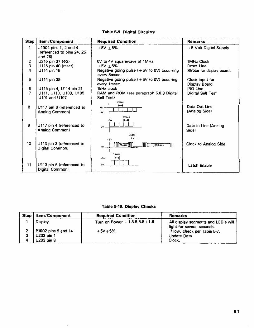
Table 59. Digital Circuitry
Step
1
2 3 4
ItemlComponent
J1004 pins 1, 2 and 4 (referenced to pins 24, 25 and 26) U315 pin 37 I*21 U115 pin 40 (reset) U114 pin 15
5 U114 pin 39
6 U115 pin 4, U114 pin 21 7 Ulll, UllO, u103, u105
UlOl and U107
ziy;;ndition 1
OV to 4V squarewave at 1 MHz +5v +5% Negative going pulse ( + 5V to OV) occurring every Emsec. Negative going pulse I + 5V to OV) occuring every 1 msec 1kHz clock RAM and ROM (see paragraph 5.8.3 Digital Self Test)
Remarks
+ 5 Volt Digital Supply
1MHz Clock Reset Line Strobe for display board.
Clock input for Display Board IRQ Line Digital Self Test
8
I U117 pin 6 (referenced to Analog Common) I Date Out Line
(Analog Side)
1%
9 U117 pin 4 (referenced to o” Analog Common)
p
.?wc -5” lt-
10 U113 pin 3 (referenced to Digital Common) 0”
11 U113 pin 8 (referenced to Digital Common)
Data in Line (Analog Side)
Clock to Analog Side
Latch Enable
Table 5-10. Display Checks
Step Item/Component Required Condition Remarks
1 1 Display Turn on Power + 1.8.8.8.8 + 1.8 1 All display segments and LED’s will
2 3 4
P1002 pins 9 and 14 U203 pin 1 U203 pin 8
+5v+5% light for several seconds. If low, check per Table 5-7. $22 D*ts
5-7
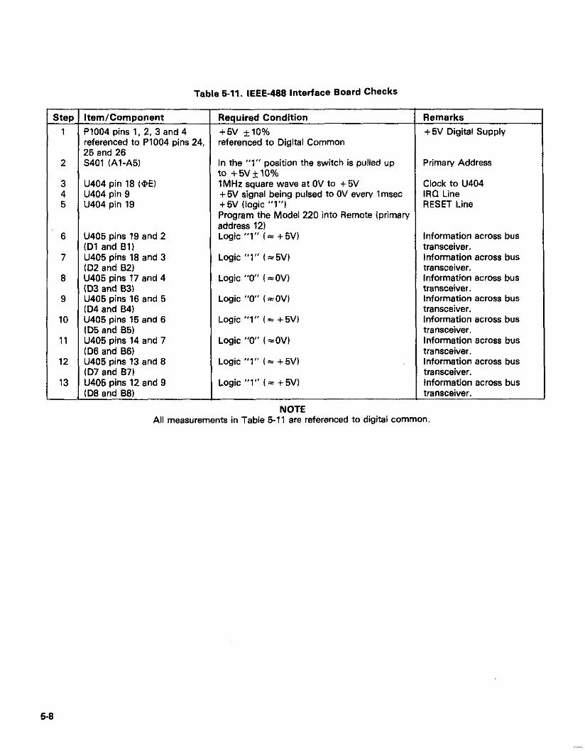
Table 6-11. IEEE-488 Interface Board Checks
Step Item/Component Required Condition Remarks
1 P1004 pins 1. 2, 3 and 4 +5v *lO% + 5V Digital Supply referenced to P1004 pins 24, referenced to Digital Common 25 and 26
2 5401 (Al-A51 In the “1” position the switch is pulled up Primary Address to +5v+lo%
3 U404 pin 18 l@Ei 1MHz square wave at OV to +5V Clock to U404 4 U404 pin 9 + 5V signal being pulsed to OV every I msec IRQ Line 5 U404 pin 19 +5V (logic “1”) RESET Line
Program the Model 220 into Remote (primary address 12)
6 U405 pins 19 and 2 Logic “1” l ii + 5VI Information across bus lD1 and Bll transceiver.
7 U405 pins 18 and 3 Logic “1” l15Vl Information across bus lD2 and 82) transceiver.
8 U405 pins 17 and 4 Logic “0” l I OVl Information across bus lD3 and 83) transceiver.
9 U405 pins 16 and 5 Logic “0” l =OVl Information across bus ID4 and B4l transceiver.
10 U405 pins 15 and 6 Logic “1” l 5 + 5Vl Information across bus lD5 and 65) transceiver.
11 U405 pins 14 and 7 Logic “0” i =OVi Information across bus lD6 and 66) transceiver.
12 U405 pins 13 and 8 Logic “1” l = + 5Vi Information across bus lD7 and 87) transceiver.
13 U405 pins 12 end 9 Logic “1” i = + 5Vl Information across bus (DE and 881 transceiver.
NOTE All measurements in Table 5-l 1 are referenced to digital common.
6-E
SECTION 6 REPLACEABLE PARTS
6.1 INTRODUCTION
This section contains replacement parts information. schematic diagrams, and component location drawings for the Model 220. An exploded view of the Model 220 is shown in Figure 6-1, while an illustration of the Fan Assembly is shown in Figure 6-2.
8.2 PARTS LIST
Parts are listed alphabetically in order of their circuit designations. Table 6-l contains an index of the schematic diagrams and component location drawings included at the end of this section. Table 6-2 contains a parts list for the Model 220 motherboard. Table 6-3 contains a parts list for the display board. Table 6-4 contains a parts list for the analog board. Table 8-5 contains a parts list for the IEEE interface board.
Table 6-l. Index of Model 220 Schematics and Component Layouts
Title
Display Board Component Layout Mother Board Component Layout Analog Board Component Layout IEEE Interface Board Component Layout Display Board Schematic Mother Board Schematic Analog Board Schematic IEEE Interface Schematic
6-6 6-7 L 6-8 5-9 6-10
6.3 ORDERING INFORMATION
To place an order, or to obtain information concerning replacement parts, contact your Keithley representative or the factory. See the inside front cover for addresses. When ordering include the following information:
1. Instrument Model Number 2. Instrument Serial Number 3. Part Description 4. Circuit Description (if applicable) 5. Keithley Part Number
8.4 FACTORY SERVICE
If the instrument is to be returned to the factory for service, complete the service form which follows this section and return it with the instrument.
6.5 SCHEMATIC DIAGRAMS AND COMPONENT LOCATION DRAWINGS
Schematic diagrams and. component location drawings follow the replaceable parts list information in the order listed in Table 6-l.
6-1

NOTE: Mechanical parts that are replaceable ,Sl
: show the appropriate part number. The parts that are labeled but do not have a part number are shown for reference purposes ally.
Figure 6-l. Model 220 Exploded View
g-2

NOTE: Mechanical parts that are replaceable show the appropriate part number. The parts that are labeled but do not have a part number are shown for reference purposes only.
Figure 6-2. Model 220 Fan Assembly
63
Table 6-2. Mother Board D220-103, Parts List
6-d
Circuit Desig.
AT101 AT102 AT103 AT104 Cl01 Cl02 Cl03 Cl04 Cl05 Cl06 Cl07 Cl08 Cl09 Cl10 Cl11 Cl12 Cl13 Cl14 Cl15 Cl16 Cl17 Cl18 Cl19 Cl20 :121-Cl2 :123 1124 CR101 CR102 CR103 CR104 CR105 CR106 CR107 CR108 CR108 CR110 CR111 CR112 FlOl FlOl FlOl FlOl JlOOl J1003 J1008 P1004 P1005 P1008 RlOl R102 R103 R104 R105 R106 R107 R108 RlOS
2
Description
Optical Isolator, 6N137 Optical Isolator, 6N137 Optical Isolator, 6N137 Optical Isolator. 6N137 .lpF, 16V. Ceramic Disc .lpF, 16V. Ceramic Disc 1OpF. 25V, Aluminum Electrolytic 68OOpF. 5OOV. Ceramic Disc .lpF, 16V. Ceramic Disc .OlpF, 5OOV. Ceramic Disc 10,OOOpF. 25V. Aluminum Electrolytic .1&F, 16V. Ceramic Disc .1&F, 16V. Ceramic Disc .1&F, 18V. Ceramic Disc .lpF, 16V. Ceramic Disc .lpF, 16V. Ceramic Disc .lpF, 16V. Ceramic Disc 22pF. 1OOOV. Ceramic Disc 22pF. 1OOOV. Ceramic Disc .llrF. 16V. Ceramic Disc 330~F. 18OV. Aluminum Electrolytic 33OfiF. 18OV. Aluminum Electrolytic lO$F, 25V. Aluminum Electrolytic 1OpF. 25V. Aluminum Electrolytic 1 OOOpF, 35V. Aluminum Electrolytic 33OpF. 5OOV. Ceramic Disc
Rectifier Bridge (5Al. PE05 Rectifier, 1 N4006 Rectifier, 1 N4006 Rectifier, 1 N4006 Rectifier, 1 N4006 Rectifier, 1 N4006 Rectifier, 1 N4006 Rectifier Bridge (1.5Al. PF-40 Rectifier, 1 N4008 Rectifier, 1 N4006 Rectifier, 1 N4006 Rectifier, 1 N4006 Fuse, 318 Amp, 25OV. Slo-Slo Fuse, 314 Amp, 25OV. Slo-Blo Fuse, 8110 Amp, 25OV. Slo-Blo Fuse, 4110 Amp, 25OV. Slo-Blo power Connector Cable Assembly (26-pin) Socket l&pin 5OOV. Connector Male 2 pin, Connector 3 pin, Molex Connector 18k. 5%. 114W. Composition 4.7k. 5%. 114W. Composition 220k. 5%. 114W, Composition 4.7k. 5% 114W, Composition 390D. 5%. 1/4W, Composition 220R, 5%. 1/4W, Composition 2.4k. 5%. 1/4W, Composition 22OQ, 5%. 1/4W, Composition 2.4k. 5%. ll4W. ComDosition
Location Sch. Pcb. Gl D4 G3 ii2
D4 D5
G3 D5 E4 02 G4 04 :; F5 D2 E5 64 ii c4 G3 F2 D3
:: D4 c4
G3 E4 G2 81 z 83 C5 83 c5 G3 D2 EZ c2 E5 03 F5 D3 F6
F5 El
c4 c2 c2 c2 c2 c3
2 G5
:z G5 A4
ii A4 A4 - H5 -
Al.81 H5 E4
:: F2 Fl G3 G3
G3 E4 E4 E4 E4 F5 F5 F5 E3 E3 E3 -
H3
ii H3 G2 E5 -
i; D2 02 D3
:: E4 D4 E4
G2 D5 G2 E5
Keithlev Part Nd.
IC-292 IC-292 IC-292 IC-292 C-238-.1 C-238-.1 c-314-10 C-22-.0068 C-238-.1 c-22-.01 C-342-10000 C-238-.1 C-238-.1 C-238-.1 C-238-.1 C-238-.1 C-238-.1 C-64.22~ C-64.22~ C-238-.1 c-337-330 c-337-330 c-314-10 c-314-10 c-309-1 000 C-22-330~ C-178-.1 RF-64 RF-38 RF-38 RF-38 RF-38 RF-38 RF-38 RF-46 RF-38 RF-38 RF-38 RF-38 FU-18 FU-19 FU-52 FU-53 CS-388 CA-lo-3 so-65 CS-389.3 CS-288-2 CS-288-3 R-76-18k R-76-4.7k R-76220k R-76-4.7k R-76-390 R-76-220 R-762.4k R-76220 R-782.4k
Table 6-2. Mother Board D220-103, Parts List (Cont.1
Circuit Desig.
RllO Rlll R112 R113 R114 R115 Rll8 RllS R121 R122 R125 R126 R127 R128 SlOl 5102 TlOl TlOl UlOl u102 u103 u104 u105 U106 u107 UlO8 UlOS UllO Ulll u112 u113 u114 u115 U116 u117 VRlOl VR102 VR103 WlOl w102 YlOl
Description
22OR. 5%. 114W. Composition 2.4k. 5%. 1/4W, Composition 4.7k. 5%. 1/4W, Composition 22OB. 5%. 1/4W, Composition Thick Film Resistor Network 4.7k. 5%. 114W. Composition lOOk, f lo%, 1/2W, Composition lOOk, f lo%, 1/2W, Composition 1OOg. * 10%. 112W. Composition 1OOg. * 10%. 112W. Composition 4.7k. 5%. 114W. Composition 10k. 5%, 114W. Composition 4.7k. 5%. 1/4W, Composition 47kB. 10%. 0.25W. Composition Switch, Power Switch. Line Transformer Transformer Transformer lspecial for SOV-1lOV 18OV-220V operationl Transformer lspecial for SOV-1lOV 18OV-220V operationl 1024 X 4bit Static Ram. 2114 1024 X 4bit Static Ram. 2114 OscillatorlClock, 4060 OscillatorlClock, 4060 1024 X 4-bit Static Ram. 2114 1024 X 4-bit Static Ram. 2114 Up/Down Counter, 74LS193 1024 X4-bit Static Ram, 2114 Quad 2-111. Nand Gate.74 LSOO 1024 X Qbit Static Ram. 2114 Clued 2-In. NOR Gate, 74LSO2 Erasable Prom, 2732 DecoderlDemultiplexer, 74LS138 Erasable Prom, 2732 Ebit Shift Register, 14094 Quad Exclusive OR Gate, 7486 Interface Adapter, SY6522 Microprocessor, MC6808 Bus Driver, 14503 Hex Inverter, 16.pin DIP, 4049 5 Volt Regulator, LM309K * 15V. 3.term, 7915 3.term Positive Voltage Regulator, 7815 Jumper Jumper 4.0 MHZ Crystal
G2 G2 Hl Gl E5
Ez D2
2 E2
El G5 A3 A3 82 82 D5 E4 c5 F4
& SEV SEV 85 F3 A5 El
SW c2 82
S’,“, D4 D3 D3 86 B6
Location Sch. Pcb.
05 E5
EE 85 c5 E5 E5 E3 E3 D4 D5 E3 E3 82 G2 F2 F2 c2 D2 c2 02 c2 02 c3 D3 c3 D3 c4 D4 D4 c4 c5 c5 E5 F4 F5 F5 D2 D2 C5
I
-
Keithley Pert No.
R-76-220 R-762.4k R-764.7k R-76-220 TF-140 R-76.4.7k R-l-look R-l-look R-1-100 R-1-100 R-754.7k R-76.10k R-784.7k R-7647k SW-466 SW-397 TR-186 TR-187 LSI-15 IC-197 LSI-15 K-214 LSI-15 K-163 LSI-15 IC-179 220-800-85 KC-182 220-801-85 IC-251 IC-118 LSI-28 LSI-27 KC-250 IC-106 IC-34 IC-174 IC-96 J-3 J-3 CR-10
8-5

Table 6-3. Display Board D220-113, Parts List
Circuit Desig.
c201 DS201 DS202 OS203 DS204 DS205 DS206 DS207 DS208 DS209 DS210 DS211 DS212 DS213 DS214 DS215 DS216 DS217 DS218 DS219 PlGu2 Cl201 Q202 cl203 a204 a205 Cl206 a207 Cl206 R.201 R202 s201 s202 S203 5204 5205 5206 5207 5208 s209 5210 s211 5212 5213 S214 S215 5216 S217 S218 S219 s220 s221 s222 5223 S224 5225 u201 u202 U203 U204
Description
1OlrF. 25V, Aluminum Electrolytic * 1, Digital Display “8” Digital Display “8” Digital Display “8” Digital Display “8” Digital Display f 1, Digital Display “8” Digital Display Pilot Light Pilot Light Pilot Light Pilot Light Pilot Light Pilot Light Pilot Light Pilot Light Pilot Light Pilot Light Pilot Light Pilot Light Cable Assembly PNP Silicon Transistor, 2N4355 PNP Silicon Transistor. 2N4355 PNP Silicon Transistor. 2N4355 PNP Silicon Transistor, 2N4355 PNP Silicon Transistor, 2N4355 PNP Silicon Transistor, 2N4355 PNP Silicon Transistor, 2N4355 PNP Silicon Transistor, 2N4355 Thick Film Thick Film Pushbutton Switch Pushbutton Switch Pushbutton Switch Pushbutton Switch Pushbutton Switch Pushbutton Switch Pushbutton Switch Pushbutton Switch Pushbutton Switch Pushbutton Switch Pushbutton Switch Pushbutton Switch Pushbutton Switch Pushbutton Switch Pushbutton Switch Pushbutton Switch Pushbutton Switch Pushbutton Switch Pushbutton Switch Pushbutton Switch Pushbutton Switch Pushbutton Switch Pushbutton Switch Pushbutton Switch Pushbutton Switch MOS to LED Segment Driver, 75492 MOS to LED Segment Driver, 75492 8-bit Shii Register, 74LS164 MOS to LED Segement Driver, 76492
Location Keithley Sch. Pcb. Part NO.
D5 c3 c-314-10 62 DD-31
:1 82 DD-30 Cl c2 DD-30 Dl c2 DD90 Dl D2 DD30 El D2 DD-31 El Ez DD-30
iz; z PL-67 PL-67
z E7. PL-67 82 PL-67
;i s2 PL-67 c2 PL-67
F3 D2 PL-67 F3 D2 PL-67 G3 PL-67 G3 z PL-67 H3 PL-67 F3 :: PL-67 A6 E4 CA-151 F5 El TG-90
TG-90 ii: E1 TG-90 H5 El TG-90
E- E2 TG-00 E2 TG-90
65 E2 TO-90 65 Ez TG-90
SEV D2 TF-16S.l SEV Fl TF-77 A3 62 SW-435 83
:; SW-435 SW-435
z D2 SW-435 A3 D2 SW-435 B4 52 SW-435 84 E2 SW-435 A4 A4 E
SW-435 SW-435
04 D3 SW-435 D3 SW-435
ii E3 SW-435 A4 E3 SW-435
F2 SW-435 FE
2 SW-434
A5 SW-435 A5 F2 SW-435 A3 F2 SW-435 03 62 SW-435 El3 F3 SW-435
SW-435 E Ei SW-435 82 F3 SW-435 62 F3 SW-435 A2 G3 SW-435
SEV 83 K-169 SEV c3 IC-16s
D3 c-127 E3 IC-169
6-6

Table 6-4. Analog Board D220-123, Parts List
Circuit Desig.
c301 C302 c303 c304 c305 C306 c307 C308 c309 c310 c311 C312 c313 c314 c315 C316 c317 C318 c319 C320 C321 c322 C323 C324 C325 C326 C327 C328 C329 c330 CR301 CR302 CR303 CR304 CR305 CR306 CR307 CR308 CR316 CR317
Description
.lpF. 16V. Ceramic Disc
.lpF, WV, Ceramic Disc
.lpF, 16V. Ceramic Disc
.OlpF. 5OOV. Ceramic Disc
.47pF, 5OV. Ceramic Film 47OpF. 5OOV. Ceramic Disc .OlpF. 5OOV. Ceramic Disc .02pF. 5OOV. Ceramic Disc .021rF, 5OOV. Ceramic Disc 47OpF. 5OOV. Ceramic Disc .OOlpF. 5OOV. Ceramic Disc 1OlrF. 25V. Aluminum Electrolytic 22OpF. 5OOV. Ceramic Disc 1OpF. 5OOV. Polystrene 1OlrF. 25V. Aluminum Electrolytic 1OpF. 25V. Aluminum Electrolytic 4.7pF. 350V. Aluminum Electrolytic .OlpF. 5OOV. Ceramic Disc .lpF, 16VDC. Ceramic Disc .02@F, 5OOV, Ceramic Disc .lpF, 16VDC. Ceramic Disc .OlpF. 500V. Ceramic Disc 4.7pF. 35OV. Aluminum Electrolytic lOpF, 25V. Aluminum Electrolytic 1OlcF. 25V. Aluminum Electrolytic O.lpF. 25OV,Metelized Polyester 1OpF. 25V. Aluminum Electrolytic .OlpF, 5OOV. Ceramic Disc .OlpF, 5OOV. Ceramic Disc 1.5&F, 25V. Aluminum Electrolytic Diode, Germanium. lN3592 Silicon Diode, lN914 Silicon Diode, lN914 Diode Dual. Low Leakage, lDlO1 Rectifier, 1 N3595 Rectifier, 1 N3595 Silicon Diode, lN914 Silicon Diode, lN914 Silicon Diode, lN914 Silicon Diode, lN914
J1003 Connector, Male K301 Relay K302 Relay K303 Relay K304 Relay K305 Relay K306 Relay K307 Relav 11301 N-Channel FET. 2N4393 (1302 N-Channel FET, PF5301 D303 N-Channel FET, 2N4392 3304 N-Channel FET, 2N4392 3305 N-Channel FET, 2N4392 WO6 N-Channel FET, 2N4392 Xl07 N-Channel FET, 2N4392 WOE N-Channel FET, 2N4392 3309 N-Channel FET, 2N4392 3310 N-Channel FET, 2N4392 -
Location Sch. Pcb.
F3 82
84 A4 c3 F5 F4 E2 c2 61 Dl D2 D3 c5 c4 F3
EC E2 E2 Fl Fl B6 66 84 66
:z G4
CE c3 D2 D3 E3 A4 B4 F2 Fl
82 SEV SEV SEV SEV SEV SEV SEV El Dl E4 F4 F4 G4 F4 F4 F4
82 Dl Dl 02 D2
E c2 c3 63 83 B3 63
2 F3 E4 E4
z F5 F5 D5 D5 D4 D4
EZ D5
ii’3 D3 63 84 85 D3 D4 F4 F5
D5 84 84
ii 85 85 85 63 B3
c3 D3
Ei c3
G4 D3
Keithlev Part Nd.
C-238.. 1 C-238-. 1 C-238-. 1 c-z-.01 C-237-.47 C-22-470~ c-22-.01 c-22-.02 c-22-.02 C-22.470~ c-22-.001 c-314-10 c-22-220p c-138.lop c-314-10 c-314-10 C-240-4.7 c-22-.01 C-238-.1 c-22-.02 C-238-. 1 c-22-.01 C-240-4.7 c-314-10 c-314-10 C-178-0.1 c-314-10 c-22-.01 c-22-.01 c-314-15 RF-39 RF-28 RF-28 DN-3 RF-43 RF.43 RF-28 RF-28 RF-28 RF-28
cs-389.3 RL-70 RL-70 RL-70 RL-70 RL-70 RL-70 RL-50 TG-130 TO-139 TG-128 TG-128 TG-128 TG-128 TG-128 TG-128 TG-128 TG-174
6-7

Table 64. Analog Board D220-123, Parts List (Cont.1
Circuit Desig.
a311 a312 a313 a314 a315 a319 a317 a319 a316 R301 R302 R303 R304 R305 R306 R307 R306 R309 R310 R311 R312 R313 R314 R315 R316 R317 R31B R319 R320 R321 R322 R323 R324 R325 R326 R327 A328 R329 R330 R331 R332 R333 R334 R335 R336 R337 R336 R339 R340 R341 R342 R343 R344 R345 R346 R347 R346 R349 R350 R351
Description
NPN-Power Transistor, 2N5190 PNP-Power Transistor, 2N5193 PNP. Transistor, Silicon, 2N3906 PNP, Transistor. Silicon, 2N3906 NPN, Silicon, 2N3904 Diode Current Unit, J505 NPN. Silicon, 2N3904 NPN. Transistor, MJ15011 PNP. Transistor. MJ15012 301k. 1%. l/BW, Metal Film 1M. l%, 0.12W. Metal Film 1OOk Pot 1OOk Pot 49.9k. 1%. l/SW, Metal Film 10k. 1%. 119W. Metal Film 6.04k. 1%. l/BW, Mete1 Film 47k. 5%. .llW, Thick Film Resistor 47k. 5%. .llW, Thick Film Resistor 47k. 5%. .llW. Thick Film Resistor 47k. 5%. .llW. Thick Film Resistor 10k. 5%. 114W. Composition lk, 5%, 1/4W, Composition 20k. 5%. ll4W. Composition 20k. 5%. 114W. Composition 301k. 1%. l/BW, Metal Film 22.2k. .t%, IlloW, Metal Film 2000 Pot 2k Pot 22.2K. 1%. l/lOW. Metal Film 20k. 1%. 1/6W, Metal Film 20k. 1%. l/BW, Metal Film Ilk, 1%. l/EW, Metal Film lOk, 5%. ll4W. Composition 20k. 5%. 114W. Composition lk. 5%. 114W. Composition 10k. 5%. 1/4W, Composition lk, 1%. l/BW, Metal Film 4.99k. 1%. l/BW, Metal Film 1.2M. 5%. 114W. Composition 4.99k. 1%. O.lZW, Metal Film 1.2M. 5%. 114W. Composition 10k. 5%. 114W. Composition 1000, 596, 114W. Composition 47OSl, 5%, 114W. Composition 4.7k. 5%. 1/4W. Composition 4.7k. 5%. 1/4W, Composition 5.6k. 5%. 114W. Composition 390, 5%. 114W. Composition 390, 5%. 114W. Composition 5.6k. 5%. 114W, Composition 1 k, 5%) 114W. Composition 10k Pot 10k. 5%. 114W. Composition 470k. 5%. 114W. Composition 47k, 5%. 114W. Composition 15k, 5%. 1/4W, Composition 2.4k. 5%. lf4W. Composition 10k. 1%. O.l2W, Metal Film lOOk, 5%. .llW, Thick Film Resistor 10k. 5%. 1/4W, Composition
Locetion Sch. Pcb.
D3 ii,” D4 E3 E4 F2 F4 Es E5
F; EE F3 E4 Fl E5 F5 62 G5 82
:z Bl B2
G5 62 G5 62 F5 62 E5 62
i: c2 c2
Dl c2 63 Dl c4 D2
z :; F5 82 F4 62 F4 63 u F4 !Z F2 c2
c3 2l c2
Ei Ei: c3 c3 62 E2 :z
2 E 63 02 83 D2
D3 :z D3 D5 F5 E
E c3 83
Cl B3 c2 83 c2 83 E2 63 D2 83 D2 83 E2 63 61 83 Bl 83 D1 83 02
SEV :i A4 D3
Keithley Part No.
TG-106 TG-107 TG-94 TG-64 TG-47 TG-140 TG-47 TG-154 TG-155 R-66-301 k R-66.1M RP-97.100k RP-97.100k R-66.49.9k R-66.10k R-66.6.04k TF-103-4 TF-103.3 TF-103.3 TF-103-4 R-76.10k R-76.lk R-7620k R-76.2.2k R-66.301k R-263.22.2k RP-97-200 RP-97.2k R-263-22.2k R-BS20k R-BE-20k R-66.ilk R-7610k R-76.20k R-76-lk A-76-10k A-66.lk R-66-4.99k R-7&1.2M R-66-4.99k R-751.2M R-76-10k R-76-100 R-76.470 R-76-4.7k R-76-4.7k R-76.5.6k R-76-39 R-76-39 R-76-5&k R-76-1 k RP-97-10k R-76.10k R-76470k R-7647k R-76.15k R-76-2.4k R-BBlOk TF-103.2 R-76-10k
6-6
Table 6-4. Analog Board D220-123, Parts List (Cont.l
Circuit Desig. R352 R353 R354 A355 R356 R357 R358 R359 R360 R361 R362 R363 R364 R365 R366 R367 R368 R369 R370 R371 R372 R373 R374 R375 R376 R377 R378 R379 R380 R381 R392 R363 R364 R385 R396 R397 R389 R369 R390 R391 R392 R393 u301 U302 u303 u304 u305 U306 u307 U308 u309 u310 u311 U312 u313 u314 u315 U316 u317 U318 u319 U320 VR301
Description 10k. 5%. 114W. Composition 2.2M. 10%. 0.25W. Comoosition 1OOk .Pot 10k Pot 1Ok Pot 10k Pot 4.75G. 2%. 1.5W. Glass Epoxy coated, Metal Oxide lOOk, 1%. 1/4W, Composition lk. 1%. 1/4W. Comoosition 53bM, 2%. l&, Glass Epoxy coated, Metal Oxide 48M. 2%. 1.5W. Glass Epoxy coated, Metal Oxide 2.2k. 5%. ll4W. Composition 24k, 5%, 1/4W. Composition lOOk, 1%. 112W. Metal Film lOOk, 1%. 1/2W, Metal Film lOa, 1%. 0.12W. Metal Film 13R. 1%. 0.12W. Metal Film 220, 10%. 1/2W, Composition 2M. 10%. 1/2W, Composition 2.2k. 5%. 1/4W. Composition 130. 1%. l/SW, Metal Film 1On. 1%. 0.12W. Metal Film 4.7k. 5%. 114W. Composition 54.lk. ,136. l.lOW, Metal Film 4.93k. .l%. l/low, Metal Film 20k. 1%. 0.12W. Metal Film 4.65M, .5%. 1/2W, Metal Film 485k. .l%. 114W. Metal Film 499iI. ,156, 1125W. Metal Film lOOIl, 0.1%. 3W Fixed 49.9k. 1%. 0.12W. Metal Film 3.57k. 1%. 0.12W. Metal Film 5k, Pot 500 Pot 10k Pot lk Pot lOOk, 5%. li4W. Composition 10k. 5%. ll4W. Composition 10k. 5%. 114W. Composition 10k. 5%. 114W. Composition 10k Pot 3.9k. 5%. 1 l4W. Film or Composition E-bit Shift Register, 14094 8.bit Shift Registor. 14094 Bbit Shift Register, 14093 Quad 2-Input AND, 4081 Duad 2-l”@ NAND, 4011 Duad Monolithic SPST CMOS Analog Switch Wide Bandwidth Dual JFET, LF353N CMOS 8-bit Multiplying D/A Converter.AD7523 Wide Bandwidth Dual JFET. LF353N Operational Amplifier, AD3247 Integrated Circuit D/A Converter,DAC80-CBI-V Operational Amplifier, AD3247 Duad Comparator, LM339 Cluad 2 input NAND, 4011 Operational Amplifier. AD3247 Hex Invefter, 16-Pin, 4049 Cluad Comparator, LM339 DecoderlDemultiplexer, 14555 Op Amp, AD515K High/Voltage, High/Current Transistor Array, VLN2003A + 5V Regulator, 7605
Location Sch. Pcb. A4 D3 84 04 E4 E4
z 03 D3 D3 E3 E3
Ei c3 63 G2 G2 Fl F2 El
is
z
23 E3 F3
::
:3”
F4 G4 G4 D4 83 84 83 F4
c4 c3 c2
SW SEV SW E5 Ez E2 El E4 F4
SEV SW
84 SEV SEV SEV
c4 c4
k4” c4 c4 c4 c4 c4 E4 E4
:: F4 F4 F4 F5 E5 F5 F5 E5 05
Fi: c4 c4
E c5 D5
c5 c5 c5 05 05 D5 D5 83
z: Cl 02 D2 c2 c2 c2 c2 c2 82 93 83 c3 c3 II3 c3 c3
02 c5 c3 86 D5
Keithley Part No. R-76.10k R-76-2.2M RP-97.100k RP-97-10k RP-97.10k RP-97.10k R-289.4.75C R-8B-100k R-76-1 k R-289.530M R-289.46M R-76.2.2k R-76-24k R-94.100k R-94.100k R-68-10 R-98-13 R-l-22 R-l-22 A-76.2.2k R-98-13 R-88-10 R-76-4.7k R-263.54.lk R-263-4.93k R-BB-20k R-265.4.85k R-264485k R-286-499 R-308-100 R-86.49.9k R-88.3.57k RP-95-5k RP-97-500 RP-97.10k RP-97-1 k R-76100k R-7610k R-76.10k R-76.10k RP-97-10k R-763.9k IC-251 IC-251 K-251 IC-136 IC-102 IC-320 IC-246 IC-321 IC-246 IC-77 IC-323 K-77 IC-219 IC-102 IC-248 IC-106 IC-219 IC-312 IC-241 IC-206 IC-93
6-9

Table 6-5. IEEE Interface Board, Parts List
Description .OlaF, 5OOV. Ceramic Disc .OlpF, 500V. Ceramic Disc lOtiF, 25V. Aluminum Electrolytic Rectifier Bridge 11.5AI. W04M Rectifier Bridge (1.5Al. W04M IEEE Bus Connecror Cable Assembly NPN, Silicon Transistor, 2N3904 4.7k, 5%. 114W. Composition 4.7k. 5%. 1/4W, Composition Thick Film Resistor Thick Film Resistor lOOn, 10%. 112W. Composition 1000. 10%. 1/2W. Composition 1OOQ. 10%. 112W. Composition lOOR, 10%. ll2W. Composition Thick Film, Resistor Network Thick Film Resistor 33fl. 10%. 1W. Composition Primary Address Switch, Bank of 5 switches E-bit Shift Register, 4094 Shift Register, 4021 Hex Inverter. 74LSO4 GPIB Adapter, 59914 Interface Bus Tranceiver, SN75160 DecoderlDemultiplexers.74LS138 Hex 3-state Buffer, 74LS367 Interface Bus Tranceiver, 75161 auad 2 input NAND gate, 74LSOO
Location Sch. Pcb.
H3 Fl c”3 Fl c3 84 El A4 El H2 F2 Cl c2 c5 c2 02 Cl c5 Cl c4 01
E Dl El
85 El A5 85 :: F5 E2 G2 E2
El E c2 D2 c3 D2
SEV D2 F3 D2 G2 E2 E4-
E‘l E E3
63 E3
Circuit Desig. c401 C402 c403 CR401 CR402 J1017 P1004 a401 R401 R402 R403 R404 R405 R406 R407 R40B R409 R410 R411 5401 u401 U402 u403 u404 u405 U406 u407 U408 u409
Keith@ Part NC. c-22-.01 c-22-.01 c-314-10 RF-46 RF-46 cs-443 CA-lo-2 TG-47 R-78-4.7k R-76-4.7k TF-102.2 TF-103-2 R-1-100 R-1-100 R-l-100 R-1-100 TF-100 TF-103-l R-2-33 sw-450.5 IC-251 IC-130 IC-186 LSI-49 IC-298 IC-182 IC-161 IC-299 IC-163
5-10
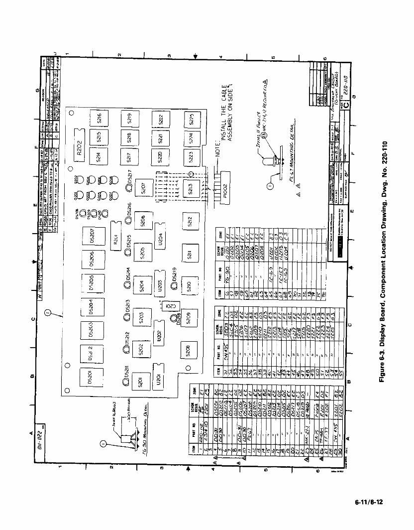
0
i--
6-11/6-12
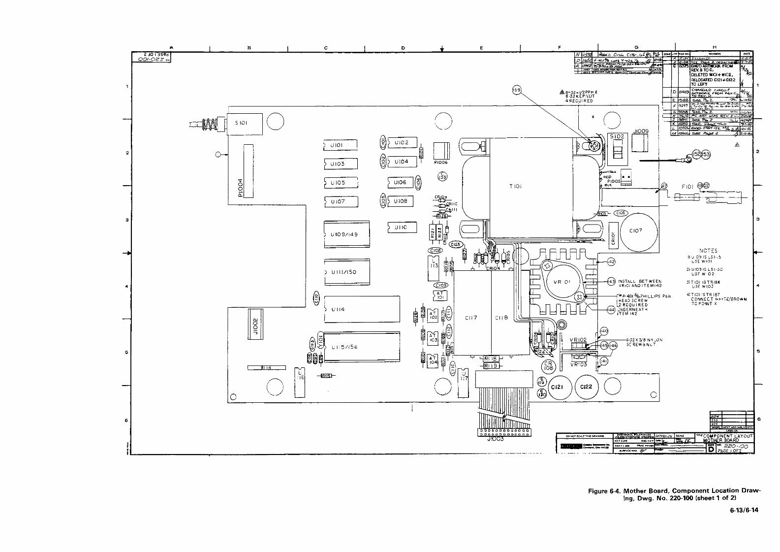
c E
J !VO3
Figure 6-4. Mother Board, Component Location Draw- ing, Dwg. No. 220-100 (sheet 1 of 21
6-1316-14
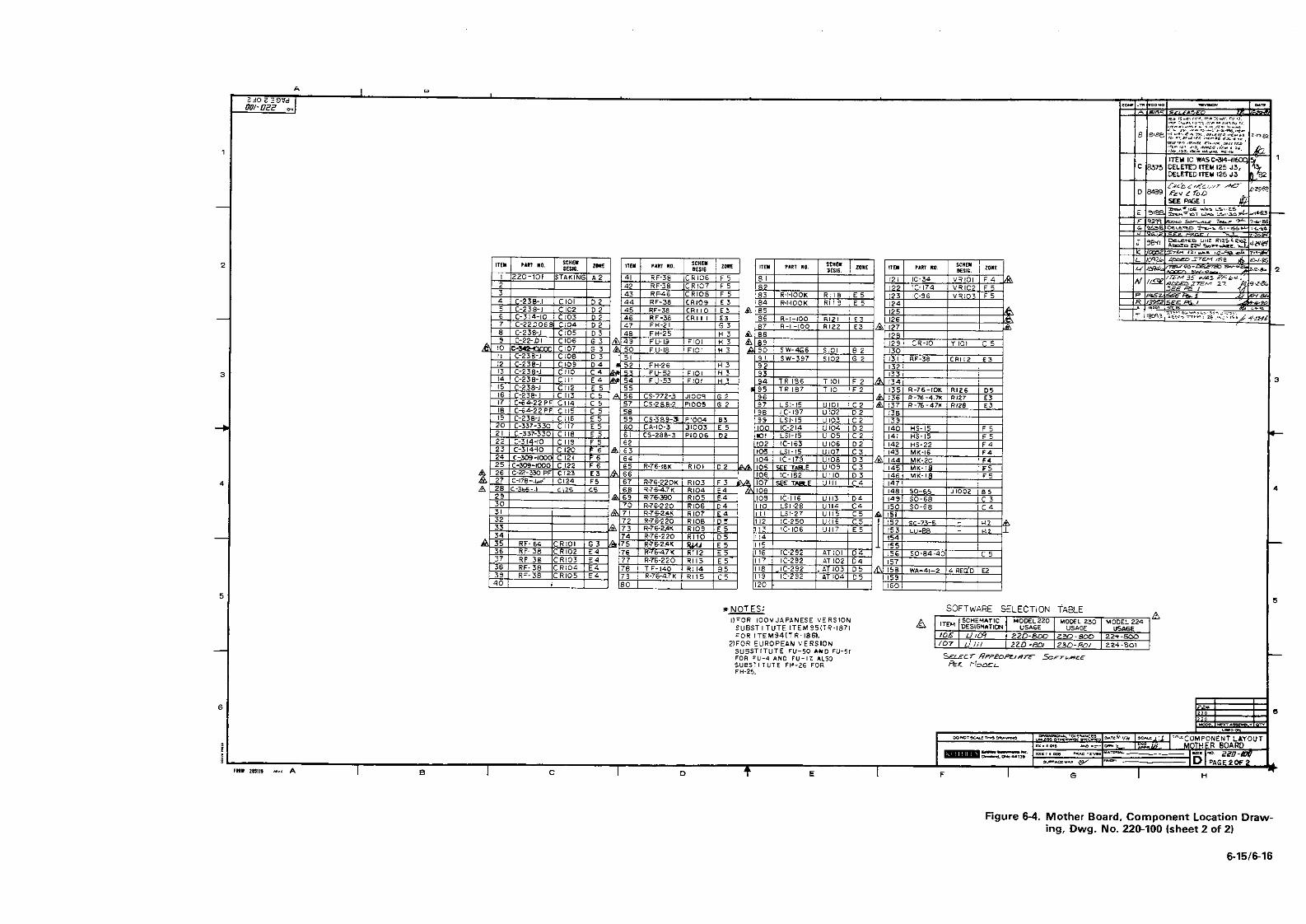
1
-
:
-
--I
4
-
5
-
6
Figure 6-4. Mother Board, Component Location Draw- ing, Dwg. No. 220-100 (sheet 2 of 2)
6-15/6-16

‘
e
-
6
I I
- / I (+-. co--I 218 ZZI
Figure 6-5. Analog Board, Component Location Draw- ing, Dwg. No. 220-120 (sheet 1 of 2)
6-1716-16
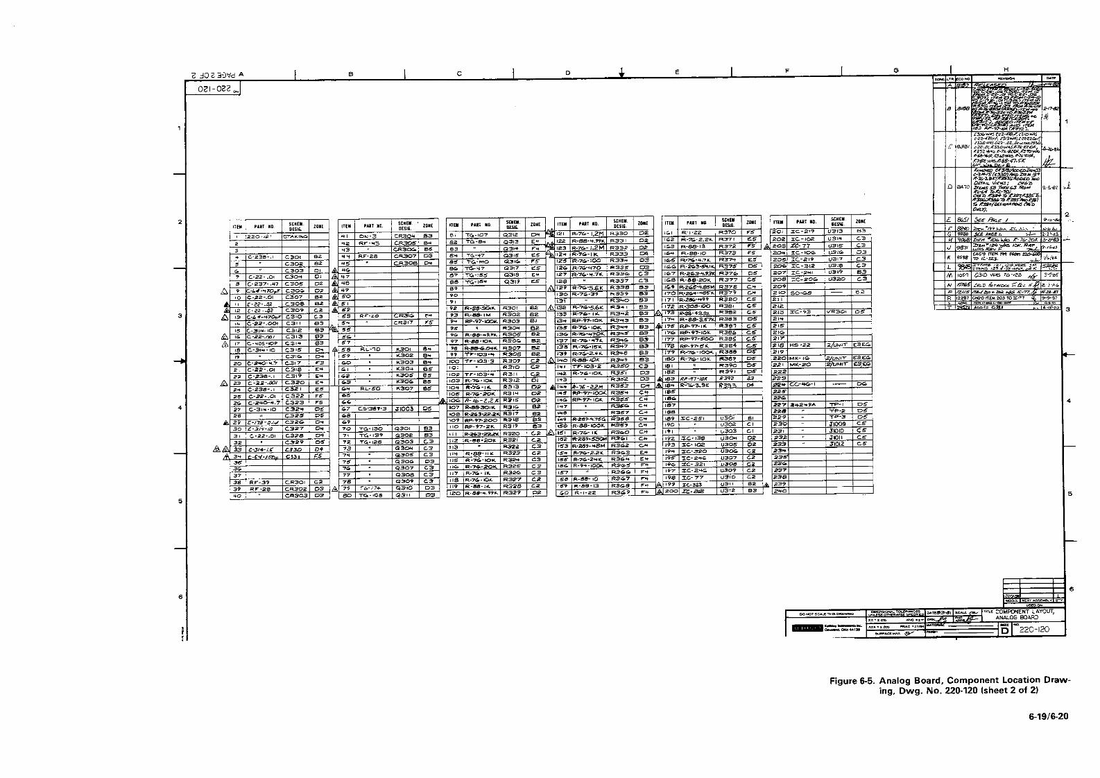
5
Figure 6-5. Analog Board, Component Location Draw- ing, Dwg. No. 220-120 (sheet 2 of 2)
6-19/6-20

N
I ”
1
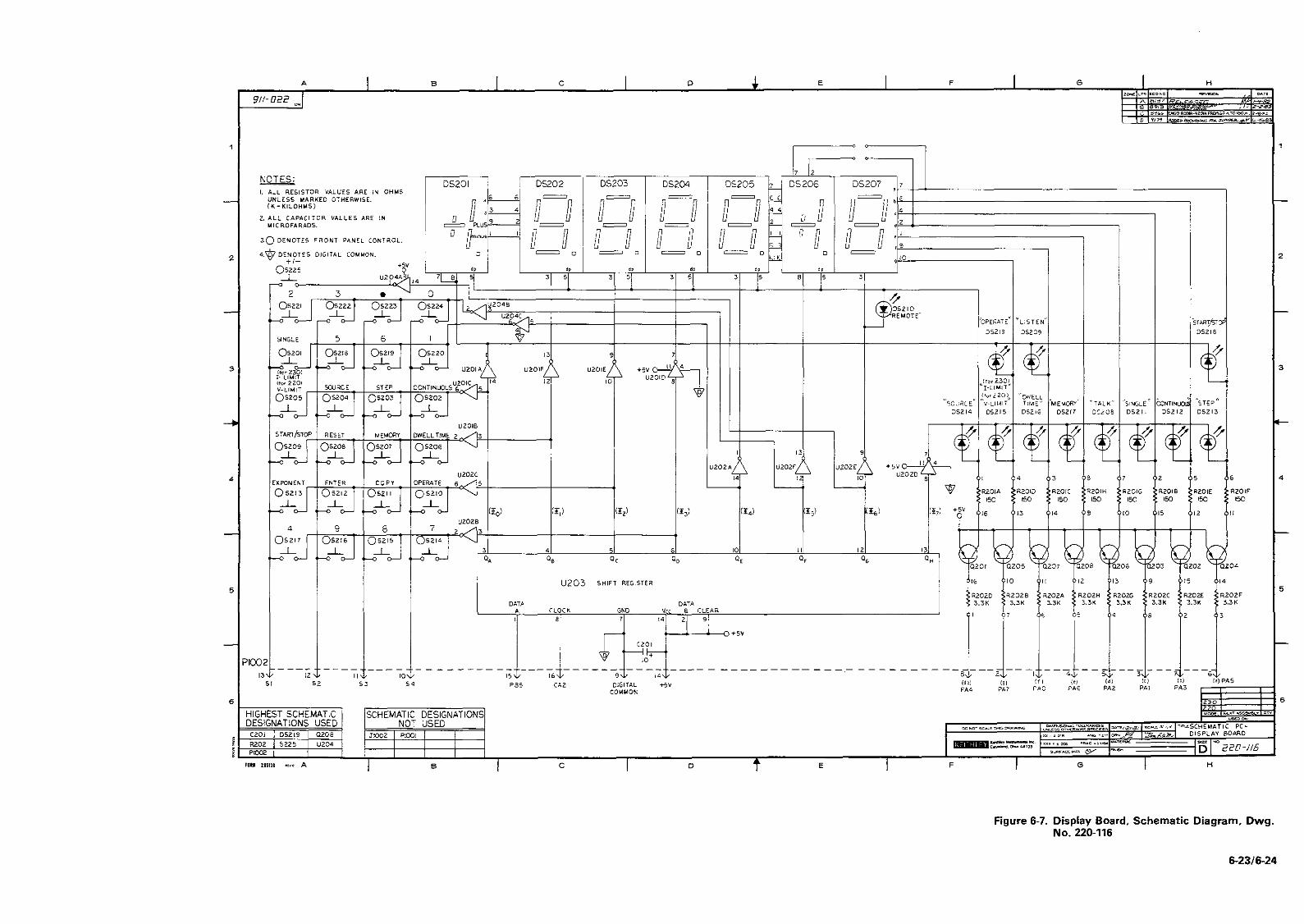
Figure 6-7. Display Board, Schematic Diagram, Dwg. No. 220-116
6-2316-24
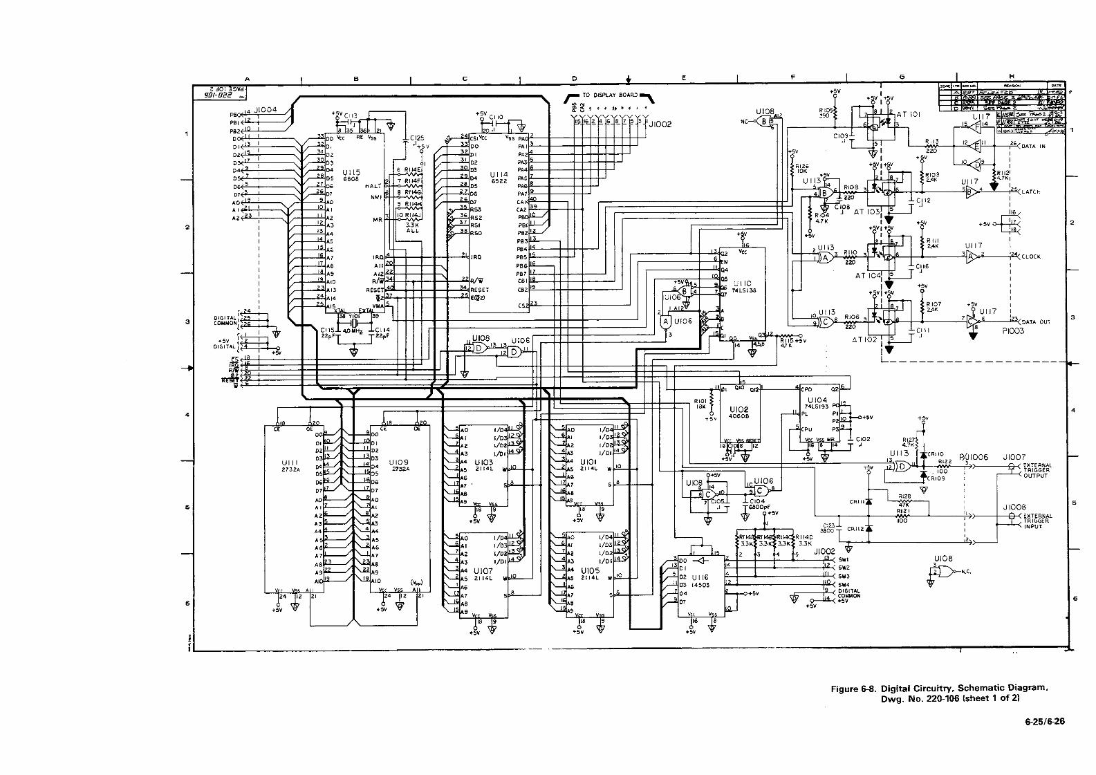
II I
- 1
Figure 6-6. Digitd Circuitry, Schematic Diagram. Dwg. No. 220-106 (sheet 1 of 21
6-251626
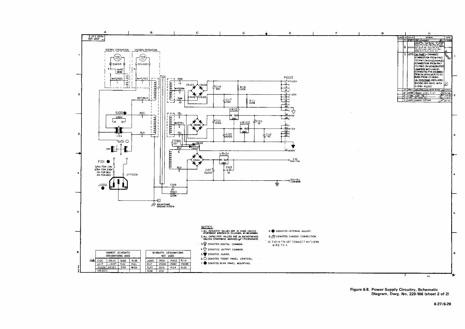
PI003
Figure 6-8. Power Supply Circuitry, Schematic Diagram, Dwg. No. 220-106 (sheet 2 of 21
62716-28
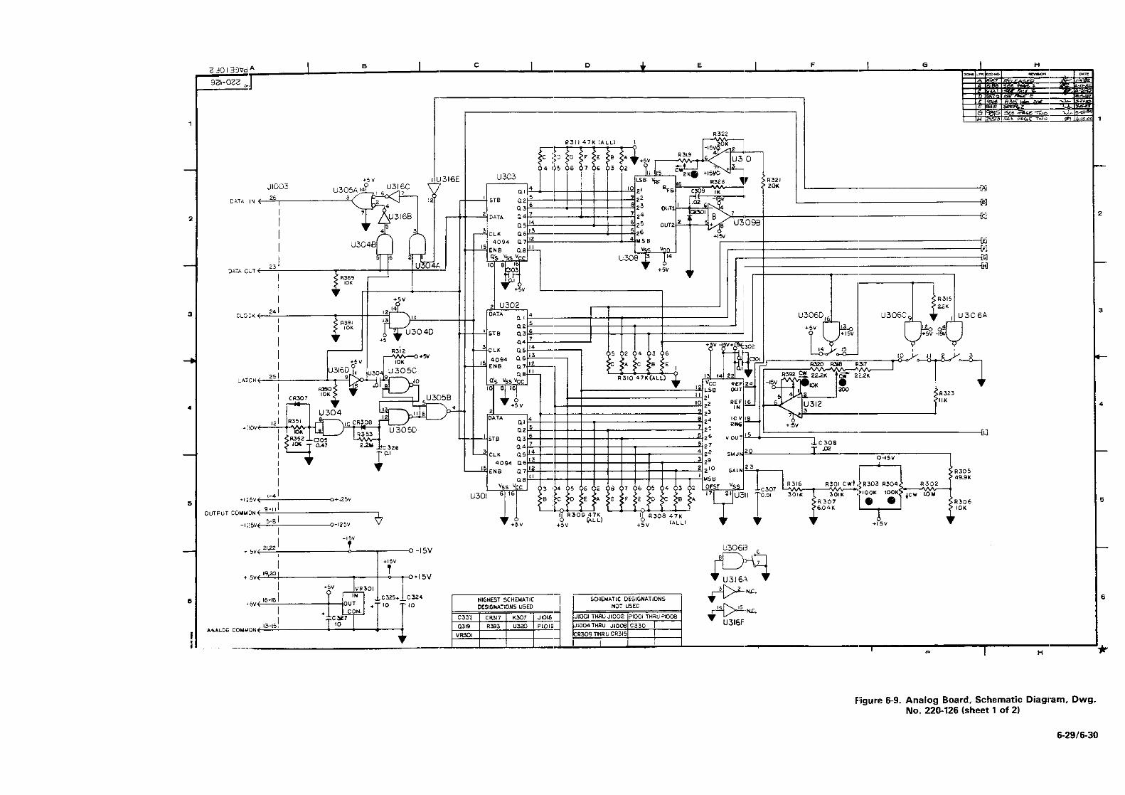
” 1
0 ul
I 0

Figure 6-9. Analog Board, Schematic Diagram, Dwg. No. 220-126 (sheet 2 of 2)
6-3116-32
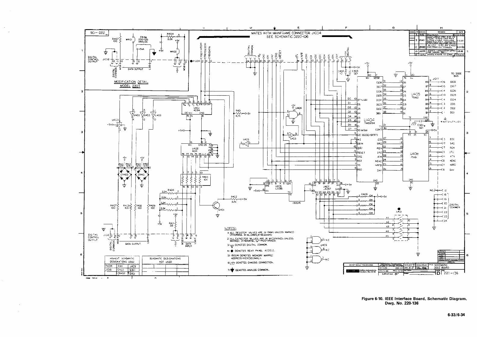
MODlFlCATlON DEVIL 2307 MODEL
Figure 6-10. IEEE Interface Board, Schematic Diagram, Dwg. No. 220-136
6-3316-34

Service Form
Model No.
Name and Telephone No.
Company
Serial No. Date
List all control settings, describe problem and check boxes that apply to problem.
Cl Intermittent
a IEEE failure D Front panel operational
Display or output (check one)
cl Drifts u Unstable B Overload
0 Analog output follows display
P Obvious problem on power-up 0 All ranges or functions are bad
0 Unable to zero 0 Will not read applied input
0 Particular range or function bad; specify
0 Batteries and fuses are OK 0 Checked all cables
0 Calibration only
0 Data required
0 Certificate of calibration required
(attach any additional sheets as necessary)
Show a block diagram of your measurement system including all instruments connected (whether power is turned on or not). Also, describe signal sowce.
Where is the measurement being performed? (factory, controlled laboratory, out-of-doors, etc.)
What power line voltage is used? Ambient temperature?
Relative humidity? Other?
Any additional information, (If special modifications have been made by the user, please describe.)

Specifications are subject to change without notice.
All Keithley trademarks and trade names are the property of Keithley Instruments, Inc. All othertrademarks and trade names are the property of their respective companies.
Keithley Instruments, Inc. 28775 Aurora Road • Cleveland, Ohio 44139 • 440-248-0400 • Fax: 440-248-61681-888-KEITHLEY (534-8453) • www.keithley.com
Sales Offices: BELGIUM: Bergensesteenweg 709 • B-1600 Sint-Pieters-Leeuw • 02-363 00 40 • Fax: 02/363 00 64 CHINA: Yuan Chen Xin Building, Room 705 • 12 Yumin Road, Dewai, Madian • Beijing 100029 • 8610-8225-1886 • Fax: 8610-8225-1892FINLAND: Tietäjäntie 2 • 02130 Espoo • Phone: 09-54 75 08 10 • Fax: 09-25 10 51 00FRANCE: 3, allée des Garays • 91127 Palaiseau Cédex • 01-64 53 20 20 • Fax: 01-60 11 77 26GERMANY: Landsberger Strasse 65 • 82110 Germering • 089/84 93 07-40 • Fax: 089/84 93 07-34GREAT BRITAIN: Unit 2 Commerce Park, Brunel Road • Theale • Berkshire RG7 4AB • 0118 929 7500 • Fax: 0118 929 7519INDIA: 1/5 Eagles Street • Langford Town • Bangalore 560 025 • 080 212 8027 • Fax: 080 212 8005ITALY: Viale San Gimignano, 38 • 20146 Milano • 02-48 39 16 01 • Fax: 02-48 30 22 74JAPAN: New Pier Takeshiba North Tower 13F • 11-1, Kaigan 1-chome • Minato-ku, Tokyo 105-0022 • 81-3-5733-7555 • Fax: 81-3-5733-7556KOREA: 2FL., URI Building • 2-14 Yangjae-Dong • Seocho-Gu, Seoul 137-888 • 82-2-574-7778 • Fax: 82-2-574-7838NETHERLANDS: Postbus 559 • 4200 AN Gorinchem • 0183-635333 • Fax: 0183-630821SWEDEN: c/o Regus Business Centre • Frosundaviks Allé 15, 4tr • 169 70 Solna • 08-509 04 600 • Fax: 08-655 26 10TAIWAN: 13F-3, No. 6, Lane 99, Pu-Ding Road • Hsinchu, Taiwan, R.O.C. • 886-3-572-9077• Fax: 886-3-572-9031
© Copyright 2003 Keithley Instruments, Inc.Printed in the U.S.A.
2/03