
MOCVD Emitter Regrowth Technology for Scaling InGaAs/InP ... · Radar Stratigraphy of the Uppermost...
129
UNIVERSITY of CALIFORNIA Santa Barbara MOCVD Emitter Regrowth Technology for Scaling InGaAs/InP HBTs to Sub-100nm Emitter Width A Dissertation submitted in partial satisfaction of the requirements for the degree Doctor of Philosophy in Electrical and Computer Engineering by Prateek Choudhary Committee in Charge: Professor Mark J. W. Rodwell, Chair Professor John E. Bowers Professor Umesh K. Mishra Professor Chris Palmstrom December 2015
Transcript of MOCVD Emitter Regrowth Technology for Scaling InGaAs/InP ... · Radar Stratigraphy of the Uppermost...
UNIVERSITY of CALIFORNIASanta Barbara
MOCVD Emitter Regrowth Technology for
Scaling InGaAs/InP HBTs to Sub-100nm
Emitter Width
A Dissertation submitted in partial satisfaction
of the requirements for the degree
Doctor of Philosophy
in
Electrical and Computer Engineering
by
Prateek Choudhary
Committee in Charge:
Professor Mark J. W. Rodwell, ChairProfessor John E. BowersProfessor Umesh K. MishraProfessor Chris Palmstrom
December 2015
The Dissertation of Prateek Choudhary is approved.
Professor John E. Bowers
Professor Umesh K. Mishra
Professor Chris Palmstrom
Professor Mark J. W. Rodwell, Committee Chair
November 2015

MOCVD Emitter Regrowth Technology for Scaling InGaAs/InP HBTs to
Sub-100nm Emitter Width
Copyright c© 2015
by
Prateek Choudhary
iii

Curriculum VitæPrateek Choudhary
Personal
Dec. 1987 Born in Sundergarh, Orissa, India.
Education
2015 Ph.D. in Electrical and Computer Engineering, University of Cal-ifornia, Santa Barbara.
2012 M.S. in Electrical and Computer Engineering, University of Cal-ifornia, Santa Barbara .
2010 B.S. in Electrical and Computer Engineering, University of Texasat Austin.
2010 B.S. in Physics (Departmental Honors), University of Texas atAustin.
Awards
2013-2014 IBM PhD Fellowship.
2009 Best Student Poster Presentation, University of Texas at AustinPhysics Open House.
2009 NASA Group Achievement Award - ”For outstanding contribu-tions to the US SHARAD radar sounder processing, analysis andvisualization capabilities”.
2009-2010 National Instruments Endowed Scholarship for Excellence.
Publications
[1] P Choudhary, C-Y Huang, JC Rode, HW Chiang, MJW Rodwell, Sub-Micron InGaAs/InP DHBTs using MOCVD Selective Emitter Regrowth withDC Current Gain of 28, in progress for IEEE Electron Device Trans. (2015)
[2] P. Choudhary, J.W. Holt, S. Kempf, D. Young, Modeling and analysis ofsurface topographic effects on the orbital radar sounding of Mars, in prepara-tion for IEEE Geoscience and Remote Sensing (2016)
[3] P Choudhary, C-Y Huang, JC Rode, HW Chiang, MJW Rodwell, In-GaAs/InP DHBTs using MOCVD Selective Emitter Regrowth, Indium Phos-phide and Related Materials (2015)
iv

[4] C-Y Huang, P Choudhary, S Lee, S Kraemer MJW Rodwell, 12 nm-gate-length ultrathin-body InGaAs/InAs MOSFETs with 8.3*105 Ion/Off, DeviceResearch Conference (2015)
[5] JC Rode, HW Chiang, P Choudhary, V Jain MJW Rodwell, Indium Phos-phide Heterobipolar Transistor Technology Beyond 1-THz Bandwidth, IEEEElectron Devices Transactions, Vol PP, Issue 99 (2015)
[6] JC Rode, HW Chiang, P Choudhary, V Jain MJW Rodwell, An In-GaAs/InP DHBT with simultaneous ft/fmax 404/901 GHz and 4.3V break-down voltage, IEEE Electron Devices Society, Vol 3, Issue 1 (2014)
[7] HW Chiang, JC Rode, P Choudhary, MJW Rodwell, Lateral carrier dif-fusion and current gain in THz InGaAs/InP DHBTs, J. Appl Physics, 115(2014)
[8] H-W Chiang, J Rode, P Choudhary, MJW Rodwell, Surface transport andDC current gain in InGaAs/InP HBTs DHBTs for THz applications, DeviceResearch Conference (2014)
[9] MJW Rodwell, S Lee, C-Y Huang, D Elias, V Chobpattanna, J Rode, H-W Chiang, P Choudhary, R Maurer, M Urteaga, B Brar, AC Gossard, SStemmer, Nanometer InP electron devices for VLSI and THz applications,Device Research Conference (2014)
[10] M.J. Rodwell, J. Rode, H. Chiang, P Choudhary, T. Reed, E. Bloch, S.Daneshgar, B. Brar, H. Park, A.C. Goassard, B. Thibeault, W. Mitchell,M. Urteaga, Z. Griffith, J. Hacker, M. Seo, THz Indium Phosphide BipolarTransistor Technology, Compound Semiconductor IC Symposium (2012)
[11] J.J. Plaut, J.W. Holt, J. W. Head, Y. Gim, P Choudhary, D. M. Baker,A. Kress, and the SHARAD Team, Thick ice deposits in deuteronilus men-sae, mars: regional distribution from radar sounding., Lunar and PlanetaryScience Conference (2010)
[12] S. Christian, J.W. Holt, P Choudhary, K. Fishbaugh, Correlating highresolution radar reflectors with visible layering of the northern polar layereddeposits, Mars, Lunar and Planetary Science Conference (2010)
[13] I.B. Smith, J. W. Holt, D. Mohrig, W. Kim, P Choudhary, QuantitativeRadar Stratigraphy of the Uppermost North Polar Layered Deposits, Mars,and Processes Controlling Spiral Trough Migration, Lunar and Planetary Sci-ence Conference (2010)
[14] N.B. Karlsson, J.W. Holt, R.C.A Hindmarsh, P Choudhary, Internal Lay-ering of Gemina Lingula, North Polar Layered Deposits, Mars, and the Casefor Ice Flow, Lunar and Planetary Science Conference (2010)
v
[15] T.C. Brothers, J.W. Holt, S. Christian, P Choudhary, Investigating Sub-surface Geomorphology of the Basal Unit of Planum Boreum, Mars withSHARAD to Constrain Early Erosional Processes, Lunar and Planetary Sci-ence Conference (2010)
[16] J.W. Holt, A. Safaeinili, J.J. Plaut, J.W. Head, R.J. Phillips, R. Seu, S.D.Kempf, P Choudhary, D.A. Young, N.E. Putzig, D. Biccari, and Y. Gim,Radar Sounding Evidence for Buried Glaciers in the Southern Mid-Latitudesof Mars, Science, vol. 322 (2008)
vi
Abstract
MOCVD Emitter Regrowth Technology for Scaling InGaAs/InP HBTs to
Sub-100nm Emitter Width
by
Prateek Choudhary
By scaling semiconductor thicknesses, lithographic dimensions, and contact
resistivities, the bandwidth of InGaAs/InP Hetero-junction Bipolar Transistors
(HBTs) has reached 550/1100 GHz ft/fmax at 128 nm emitter width (wE). Pri-
mary challenges faced in scaling the emitter width are: developing high aspect
ratio emitter metal process for wE < 100nm, reducing base contact resistivity
ρb,c, and maintaining high DC current gain β.
The existing W/TiW emitter process for RF HBTs cannot scale below 100
nm. Process modules for scaling the emitter width to 60 nm are demonstrated.
High aspect ratio trenches are etched into a sacrificial Si layer and then filled
with metal via Atomic Layer Deposition (ALD). Metals with high melting points
are chose to withstand high emitter current densities (JE) at elevated junction
temperatures without suffering from electromigration or thermal decomposition
and is thus manufacturable. ALD deposition of TiN, Pt, and Ru are explored.
Novel base epi designs are proposed for reducing Auger recombination current
(IB,Auger). A dual doping layer in the base is proposed with a higher doping in the
upper 5 nm of the base for lower ρb,c and a lower doping in the remainder of the
base for reducing IB,Auger. Presence of a quasi-electric field (4EC) in the upper
vii

doping grade accelerates electrons away from the region towards the collector,
thus further reducing IB,Auger.
Selective regrowth of the emitter semiconductor via Metal-Organic Chemical
Vapour Deposition (MOCVD) is proposed for decoupling the extrinsic base region
under the base metal from the intrinsic region under the emitter-base junction,
for increasing β,ft, and improving ρb,c. Carbon p-dopants in the InGaAs base are
passivated by H+ during regrowth. Annealing to reactivate carbon induces surface
damage and increases base sheet resistance (Rb,sh) and ρb,c. Process techniques
for minimizing Rb,sh and ρb,c in an emitter regrowth process are demonstrated
and compared. ρb,c of 5.5 Ω.µm2 on p-InGaAs is demonstrated on Transmission
Line Measurement (TLM) structures after regrowth and anneal, by protecting the
semiconductor surface with tungsten. This is comparable to 2.9 Ω.µm2 measured
on TLM structures that do not undergo regrowth and anneal.
Feasibility of emitter regrowth is demonstrated on Large Area Devices (LADs)
with SiO2 as regrowth mask, and W cap during anneal. Emitter-regrowth and
non-regrowth devices of identical dimensions and epi design are compared. Emitter-
regrown HBTs yield higher β of 28 as compared to 13 for non-regrowth devices.
Benefits of emitter regrowth cannot be ascertained on LADs due to high series
resistance and large gap spacings between base metal and emitter-base junction.
A process flow is proposed for scaling regrown HBTs to 60 nm emitter widths.
The process incorporates ALD emitter metal technology that is demonstrated in
the first half of the dissertation. New epi designs for regrown-emitter HBTs are
optimized for maximizing β, ft. Scaling regrown-emitter HBTs is essential for
realizing their benefit over non-regrowth HBTs.
viii

Contents
Curriculum Vitæ iv. . . . . . . . . . . . . . . . . . . . . . . . . . . . . . . . . . . . . . . . iv
Abstract vii
List of Tables xii
List of Figures xiv
1 Introduction 1References . . . . . . . . . . . . . . . . . . . . . . . . . . . . . . . . . . 5
2 HBT Theory 72.1 Device Structure . . . . . . . . . . . . . . . . . . . . . . . . . . . 7
2.1.1 Principle of Operation . . . . . . . . . . . . . . . . . . . . 72.1.2 HBT Emitter Design . . . . . . . . . . . . . . . . . . . . . 112.1.3 HBT Base Design . . . . . . . . . . . . . . . . . . . . . . . 152.1.4 HBT Collector Design . . . . . . . . . . . . . . . . . . . . 172.1.5 HBT Equivalent Circuit Model . . . . . . . . . . . . . . . 19
2.2 HBT RF Performance and Scaling . . . . . . . . . . . . . . . . . . 212.3 DC Current Gain β . . . . . . . . . . . . . . . . . . . . . . . . . . 23
2.3.1 Schockley-Read-Hall and Radiative Recombination Current(ISRH,Irad) . . . . . . . . . . . . . . . . . . . . . . . . . . . 25
2.3.2 Auger Recombination Current (IAuger) . . . . . . . . . . . 252.3.3 Lateral Diffusion Current (IDiff) . . . . . . . . . . . . . . . 272.3.4 Surface Recombination and Conduction Current
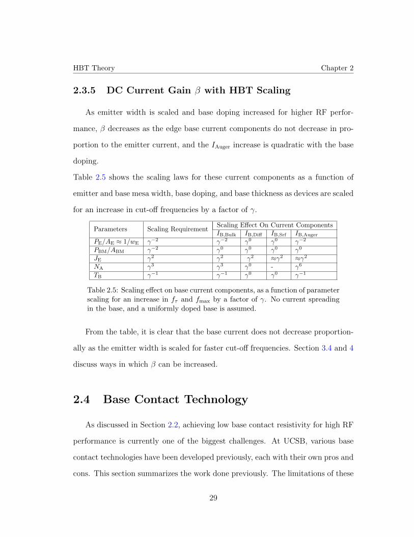
(Isrf,rec, Isrf,cond) . . . . . . . . . . . . . . . . . . . . . . . . 282.3.5 DC Current Gain β with HBT Scaling . . . . . . . . . . . 29
2.4 Base Contact Technology . . . . . . . . . . . . . . . . . . . . . . . 29
ix
2.4.1 Lift-Off Pt/Ti/Pd/Au Contacts . . . . . . . . . . . . . . . 302.4.2 Refractory Metal Contacts . . . . . . . . . . . . . . . . . . 302.4.3 Blanket Pt/Ru Metal Contacts . . . . . . . . . . . . . . . 32
References . . . . . . . . . . . . . . . . . . . . . . . . . . . . . . . . . . 34
3 RF HBT Improvements 373.1 Reducing Thermal Shock For Improved Yield . . . . . . . . . . . 373.2 Blanket Iridium Base Contacts . . . . . . . . . . . . . . . . . . . . 393.3 Epitaxial Design For JE > 40mA/µm2 . . . . . . . . . . . . . . . 413.4 Reducing Auger Recombination . . . . . . . . . . . . . . . . . . . 433.5 Atomic Layer Deposition of Emitter Metal . . . . . . . . . . . . . 44
3.5.1 ALD Emitter Challenges . . . . . . . . . . . . . . . . . . . 473.5.2 ALD Emitter Preliminary Results . . . . . . . . . . . . . . 53
References . . . . . . . . . . . . . . . . . . . . . . . . . . . . . . . . . . 54
4 MOCVD Emitter Regrowth 564.1 Device Structure . . . . . . . . . . . . . . . . . . . . . . . . . . . 564.2 Base Diffusion Current (Ib,diff) Suppression . . . . . . . . . . . . . 594.3 Reduction Of Auger Recombination In The Base . . . . . . . . . . 604.4 Increase in ft . . . . . . . . . . . . . . . . . . . . . . . . . . . . . 604.5 Regrowth as a Viable Technology . . . . . . . . . . . . . . . . . . 614.6 Self-Aligned Emitter Regrowth HBT Process . . . . . . . . . . . . 64References . . . . . . . . . . . . . . . . . . . . . . . . . . . . . . . . . . 67
5 Experimental Results and Analysis 695.1 Carbon Passivation of p-InGaAs Base . . . . . . . . . . . . . . . . 695.2 Large Area Device HBT Emitter Regrowth Process . . . . . . . . 715.3 HBT 68Q4 - Oxide Protective Cap . . . . . . . . . . . . . . . . . 73
5.3.1 Device Structure and Process Feature . . . . . . . . . . . . 735.3.2 TEM Analysis . . . . . . . . . . . . . . . . . . . . . . . . . 745.3.3 DC Characteristics . . . . . . . . . . . . . . . . . . . . . . 75
5.4 Ohmic Contacts To p-InGaAs After Regrowth . . . . . . . . . . . 775.5 Buried W as Regrowth Mask . . . . . . . . . . . . . . . . . . . . . 795.6 HBT 70R4 - InP Protective Cap . . . . . . . . . . . . . . . . . . . 82
5.6.1 Device Structure and Process Feature . . . . . . . . . . . . 825.6.2 TEM Analysis . . . . . . . . . . . . . . . . . . . . . . . . . 845.6.3 Issues and Improvements . . . . . . . . . . . . . . . . . . . 85
5.7 HBT 74 Q4 - W Annealing Cap . . . . . . . . . . . . . . . . . . . 875.7.1 Device Structure and Process Feature . . . . . . . . . . . . 875.7.2 TEM Analysis . . . . . . . . . . . . . . . . . . . . . . . . . 89
x
5.7.3 Transistor DC Characteristics . . . . . . . . . . . . . . . . 915.8 W Base Contact Yield . . . . . . . . . . . . . . . . . . . . . . . . 92References . . . . . . . . . . . . . . . . . . . . . . . . . . . . . . . . . . 96
6 Conclusion 976.1 Accomplishments . . . . . . . . . . . . . . . . . . . . . . . . . . . 97
6.1.1 Improving RF HBT Design and Process . . . . . . . . . . 976.1.2 Process Development For WE < 100nm . . . . . . . . . . . 996.1.3 MOCVD Selective Emitter Regrowth of HBT LADs . . . . 100
6.2 Future Work . . . . . . . . . . . . . . . . . . . . . . . . . . . . . . 1016.2.1 Alternate Base Contact Technologies . . . . . . . . . . . . 1016.2.2 Pulse InP Regrowth Cap . . . . . . . . . . . . . . . . . . . 1026.2.3 Epitaxial Design For Emitter Regrowth . . . . . . . . . . . 1036.2.4 Scaling HBTs for RF Performance . . . . . . . . . . . . . . 104
References . . . . . . . . . . . . . . . . . . . . . . . . . . . . . . . . . . 105
A HBT 64 Equivalent Circuit Model 106References . . . . . . . . . . . . . . . . . . . . . . . . . . . . . . . . . . 108
B UCSB W/TiW Emitter Metal Process 109References . . . . . . . . . . . . . . . . . . . . . . . . . . . . . . . . . . 111
xi

List of Tables
2.1 Typical emitter epi design of an RF HBT at wE of 100nm. . . . . 112.2 Typical base epi design of an RF HBT at wE of 100nm. . . . . . . 152.3 Typical collector epi design of an RF HBT at wE of 100nm. . . . . 182.4 Scaling laws of HBTs: the required change for improving fτ and
fmax by a factor of γ. . . . . . . . . . . . . . . . . . . . . . . . . . 222.5 Scaling effect on base current components, as a function of parame-
ter scaling for an increase in fτ and fmax by a factor of γ. No currentspreading in the base, and a uniformly doped base is assumed. . . 29
3.1 Optimized emitter epi design for JE of 50 mA/µm2 . . . . . . . . 43
4.1 Potential epi design of the extrinsic and intrinsic base in an RFHBT with regrown emitter. . . . . . . . . . . . . . . . . . . . . . 58
4.2 Energy barrier and quasi-electric field ~εQuasi that suppress Ib,diff ineach of the proposed regrowth base designs. . . . . . . . . . . . . 60
4.3 Base access resistance comparison for the proposed regrowth de-signs, compared with a non-regrowth device HBT 64C fabricatedat UCSB with a 20nm base [2]. Emitter width of 100 nm is assumed 61
5.1 Hall hole carrier concentration of p-InGaAs films after various pro-cessing and anneal conditions. . . . . . . . . . . . . . . . . . . . . 70
5.2 Epitaxial structure of HBT 68. The emitter-base junction is formedat the Emitter-Intrinsic base interface, and the extrinsic base lieson either side of this junction, on top of the intrinsic base. . . . . 73
5.3 Measured contact resistivity to p-InGaAs on TLM test structuresfor various process samples. Hall carrier concentration of 1*102cm−3
was measured on all samples before processing. Samples A and Bindicate that SiO2 is an insufficient cap and damages the surface. 79
xii
5.4 Epitaxial structure of HBT 70. The emitter-base junction is formedat the Emitter-Intrinsic base interface, and the extrinsic base lieson either side of this junction, on top of the intrinsic base. . . . . 83
5.5 Epitaxial structure of HBT74. The emitter-base junction is formedat the Emitter-Intrinsic base interface, and the extrinsic base lieson either side of this junction, on top of the intrinsic base. . . . . 88
6.1 Proposed epitaxial structure of RF HBT with emitter regrowth.The emitter-base junction is formed at the emitter-intrinsic baseinterface, and the extrinsic base lies on either side of this junction,on top of the intrinsic base. . . . . . . . . . . . . . . . . . . . . . 104
A.1 Epitaxial structure of HBT 64. . . . . . . . . . . . . . . . . . . . . 106
xiii

List of Figures
2.1 A simplified schematic of a BJT is shown on the left. The corre-sponding band diagram is shown on the right with the fermi levelEF, conduction band EC, and valence band EV labeled accordingly. 8
2.2 Band diagram of a BJT in forward-active mode illustrating major-ity carrier drift-diffusion. . . . . . . . . . . . . . . . . . . . . . . . 9
2.3 Band diagram of an abrupt InP/InGaAs HBT in forward-activemode. There exists a diffusion barrier 4EV for holes diffusing frombase to emitter. . . . . . . . . . . . . . . . . . . . . . . . . . . . . 11
2.4 Band diagram of a graded InP/InGaAs HBT in forward-activemode with the space charge region in the emitter graded from InPto InGaAs. The diffusion barrier is now 4EG for holes diffusingfrom base to emitter. . . . . . . . . . . . . . . . . . . . . . . . . . 12
2.5 Cross-sectional schematic of a UCSB RF HBT. . . . . . . . . . . 132.6 Cross-sectional TEM image of a UCSB RF HBT. . . . . . . . . . 142.7 Band diagram of the emitter region at increasing emitter-base bi-
ases. Emitter starvation occurs at sufficiently high JE [1]. . . . . . 152.8 Cross-sectional schematic of distributed RC network in the base-
collector region of an HBT. The device is symmetric along thedashed line i.e. only one side of the device is shown. . . . . . . . . 17
2.9 Hybrid-π equivalent circuit model of a BJT. . . . . . . . . . . . . 202.10 Scaling roadmap for InP/InGaAs HBTs [15] . . . . . . . . . . . . 222.11 HBT DC current gain β plotted as a function of emitter perime-
ter/area. Experimental and simulated data points show a drop inβ as the emitter width is reduced. [16] . . . . . . . . . . . . . . . 23
2.12 A cross-sectional schematic of an HBT that shows the various basecurrent components. . . . . . . . . . . . . . . . . . . . . . . . . . 24
xiv
2.13 The three band-to-band Auger processes are shown. The electronsare represented by closed circles and holes by open circles. Arrowsindicate electrons transitions [20]. . . . . . . . . . . . . . . . . . . 26
2.14 A cross-sectional TEM image shows the Pt/Ti/Au base contactsinking into the p-InGaAs base. [16]. . . . . . . . . . . . . . . . . 31
2.15 A cross-sectional TEM image shows the Ru/Ti/Au base contactwith no discernible metal sinking. [7]. . . . . . . . . . . . . . . . . 32
2.16 A cross-sectional TEM image shows the Pt/Ru/Ti/Au base con-tact. The metal sinking depth has been reduced compared to lifted-off base contact technology [7]. . . . . . . . . . . . . . . . . . . . . 33
3.1 A cross-sectional TEM image of HBT61B. The semiconductor atthe InP/InGaAs emitter-base boundary is cracked due to strain.(Courtesy: Han-Wei Chiang) . . . . . . . . . . . . . . . . . . . . 38
3.2 Process flow incorporating the low temperature SiN anchor to pro-vide structural stability. Steps (c) and (f) introduce strain on thehigh aspect ratio emitter metal as BCB and InP/W have differentcoefficients of thermal expansion. . . . . . . . . . . . . . . . . . . 39
3.3 Angled SEM image of sample after Ir dry etch. The W/TiW emittermetal has been etched due to insufficient protection during the etch.(a) Emitter (b) Vernier test structures. . . . . . . . . . . . . . . . 40
3.4 Cross-sectional SEM image of test HBT structure after Ir dry etch.The Al2O3/SiN composite sidewall protects the W/TiW emittermetal. . . . . . . . . . . . . . . . . . . . . . . . . . . . . . . . . . 41
3.5 Calculated JE as a function of electron Fermi Level (Efn) positionrelative to conduction band edge (EC) for InP emitter for Boltz-mann approximation, FermiDirac distribution function and includ-ing a non-zero electron flux reflectance at the heterointerface [10] 42
3.6 (Left) Pulse layer + doping grade profile in the base for lowRBase,cont.
[5]. (Right) Dual doping grade profile in the base maintains highdoping under base contact for low RBase,cont., but also introduces4EC in high doping regions to accelerate electrons away and re-duce Auger recombination. . . . . . . . . . . . . . . . . . . . . . . 45
3.7 Auger recombination for dual doping grade and pulse doping basedesigns, plotted as a function of base depth. . . . . . . . . . . . . 46
3.8 Schematics of 256, 128, and 64nm wide emitter metal stacks afteremitter metal dry etch. [12] . . . . . . . . . . . . . . . . . . . . . 47
3.9 Process flow for fabricating emitter metal via ALD deposition.HBT fabrication steps after (g) are identical to W/TiW emitterHBT process flow shown in Appendix B. . . . . . . . . . . . . . . 48
xv

3.10 Cross-sectional SEM images of Si trenches on the same die. Theetch rate/depth decreases as the trench width shrinks due to loadingeffects. . . . . . . . . . . . . . . . . . . . . . . . . . . . . . . . . . 49
3.11 Cross-sectional SEM images of Si trenches that bows outwards inthe middle. This leads to a hollow ’teardrop’ when ALD TiN isdeposited. The deposited TiN film thickness in the trench is nearlyhalf of the thickness in the field. . . . . . . . . . . . . . . . . . . . 50
3.12 Cross-sectional SEM images of 70nm wide high aspect ratio Sitrenches. . . . . . . . . . . . . . . . . . . . . . . . . . . . . . . . . 50
3.13 Cross-sectional SEM images Si trenches after blanket ALD TiNdeposition. (a) TiN deposition rate inside the trench is lower dueto large precursor mean free path. (b) Complete fill-in due to doseand soak process. . . . . . . . . . . . . . . . . . . . . . . . . . . . 51
3.14 Angled SEM image of Pt emitter after blanket Si etch. The emitterregion exposed to Si etch has been attacked. . . . . . . . . . . . . 52
3.15 Angled SEM image an ALD Emitter based HBT after device iso-lation. The base post (BP), collector contact (CC), base contact(BC), and emitter metal are marked. . . . . . . . . . . . . . . . . 53
4.1 Cross-sectional schematic of an emitter regrowth structure. . . . . 574.2 Simplified distributed RC network in the base-collector region. The
base gap resistance is a function of the intrinsic as well as extrinsicbase sheet resistance. . . . . . . . . . . . . . . . . . . . . . . . . . 58
4.3 (a) Electrons scatter at the base-emitter junction and diffuse to-wards the base metal in the direction XX’. (b) Band diagram showsthat electrons diffusing from emitter-base junction -at energy Einj-encounter an energy barrier 4EB in diffusing towards the basemetal, thus reducing IB,diff . . . . . . . . . . . . . . . . . . . . . . . 59
4.4 Process flow for fabricating emitter regrowth HBTs with a self-aligned emitter metal deposited via ALD. HBT fabrication stepsafter (g) are identical to W/TiW emitter HBT process flow shownin Appendix B. . . . . . . . . . . . . . . . . . . . . . . . . . . . . 65
5.1 Process flow for a Large Area Device (LAD) HBT with emitterregrowth. Steps after (i) are identical to RF HBT process in Ap-pendix B. . . . . . . . . . . . . . . . . . . . . . . . . . . . . . . . 72
5.2 Cross-sectional TEM image of HBT 68Q4 and a close-up of theemitter-base interface. It can be seen that the emitter semiconduc-tor does not contact the extrinsic base. . . . . . . . . . . . . . . . 74
xvi
5.3 Cross-sectional TEM of the base surface and base contact of HBT68Q4. The base surface is damaged. . . . . . . . . . . . . . . . . . 75
5.4 HBT 68Q4 Emitter-Base and Base-Collector diode I-V character-istics. . . . . . . . . . . . . . . . . . . . . . . . . . . . . . . . . . . 76
5.5 HBT 68Q4 gummel curve at zero base-collector bias. Collectorleakage current IC at low VBE is due to extremely high Rbb . . . . 76
5.6 TLM split to determine source of base surface damage. . . . . . . 785.7 Cross-sectional SEM of a regrowth window after the buried W has
been wet-etched using AZ300MiF. The undercut is visible at thetrench corner. The extrinsic base is then digitally etched and theemitter is regrown. . . . . . . . . . . . . . . . . . . . . . . . . . . 80
5.8 Cross-sectional SEM image of regrowth trench post regrowth. Thereis growth nucleation in select areas of the window only. This sug-gests presence of a residual layer at the surface that is inhibitinggrowth. . . . . . . . . . . . . . . . . . . . . . . . . . . . . . . . . 81
5.9 Cross-sectional SEM image of buried W regrowth after additionalCF4/O2 descum. The regrowth morphology is rough and there isvoiding in the InGaAs base. . . . . . . . . . . . . . . . . . . . . . 81
5.10 Process flow for emitter regrowth HBT LAD that incorporates anInP cap above the base for minimizing surface damage before basecontact metal deposition. The process after (d) is identical to Fig-ure 5.1, except that the W/Ti/Au base metal is deposited prior toALD oxide and anneal. . . . . . . . . . . . . . . . . . . . . . . . . 83
5.11 Cross-sectional TEM image of HBT70R4. . . . . . . . . . . . . . . 855.12 Cross-sectional TEM image of the emitter regrowth in HBT70R4.
The emitter semiconductor has been etched away during the InPcap wet etch. . . . . . . . . . . . . . . . . . . . . . . . . . . . . . 86
5.13 Cross-sectional TEM image of HBT74Q4. . . . . . . . . . . . . . . 895.14 Cross-sectional TEM image of the base mesa region of HBT74Q4.
There is voiding in the base where W/Ti/Au is present on the surface. 905.15 Cross-sectional SEM image of the base region after annealing with
a W/SiO2 cap (left) and a W/Ti/Au/SiO2 cap(right). The p-InGaAs shows voids if Ti/Au is present. . . . . . . . . . . . . . . 90
5.16 HBT 74Q4 and HBT 74Q1 emitter-base diode characteristics. HBT74Q1 devices show large variation in Rpar. Shunt between emitter-base metal is suspected. . . . . . . . . . . . . . . . . . . . . . . . 92
5.17 HBT 74Q4 and HBT 74Q1 base-collector diode characteristics.HBT74Q1 has high Rseries. Sub-collector surface contaminationprior to contact metal deposition is suspected. . . . . . . . . . . . 93
xvii
5.18 HBT74Q4 and HBT74Q1 gummel curves. The regrown-emitterHBT (74Q4) shows higher β of 28 as compared to 13 for 74Q1, atVCB=0. It is unclear if this is due to higher RBE,series and lowerRBC,series. . . . . . . . . . . . . . . . . . . . . . . . . . . . . . . . . 94
5.19 HBT 74Q4 and HBT 74Q1 common-emitter characteristics. 74Q1shows quasi-saturation as IB is increased. . . . . . . . . . . . . . . 94
5.20 Inverse DC current gain (1/β) vs HBT emitter periphery to arearation (PjE/AjE of HBT 74Q4. . . . . . . . . . . . . . . . . . . . . 95
A.1 Equivalent circuit model of HBT 64C. AE = 0.22×2.9 µm2 . . . . 107
B.1 Flow chart for HBT fabrication with blanket W/TiW emitter pro-cess [3] . . . . . . . . . . . . . . . . . . . . . . . . . . . . . . . . . 110
xviii

Chapter 1
Introduction
InP/InGaAs heterojunction bipolar transistors (HBTs) today exhibit higher band-
width than RF CMOS, HEMTs, Si/SiGe HBTs, and InGaP/GaAs HBTs at a
given lithographic feature size. The electron transit time in HBTs is largely gov-
erned by epitaxial thickness since it is a vertical device. Due to this, HBTs deliver
high linearity, power-added-efficiency and breakdown simultaneously while deliv-
ering high output power [1] [2].
The demand for high frequency transistors is fueled by sub-mm wave ra-
dio systems [3], high frequency communication systems [4], and high resolu-
tion radar/imaging systems [5] [6]. The unity current and power gain cutoff
frequency (ft, fmax) of HBTs has improved rapidly over the years [7] [8]. The
fastest HBTs reported to date have ft/fmax > 0.52/1.1 THz at the 130 nm Emit-
ter width [9]. This is exceeded only by InP HEMTs at 25 nm gate length with
ft/fmax > 0.76/1.42THz [10] [11], though InP DHBTs have demonstrated higher
open-circuit breakdown voltage [12].
1

Introduction Chapter 1
In InP/InGaAs HBT, electrons emitted from the InP emitter travel through
a thin InGaAs base (wBase λe) at high velocities due to a low electron effective
mass (InGaAs: 0.045m0). Electron velocity through the InP collector is in excess
of their Fermi velocity due to large Γ-L valley separation in the InP conduction
band [13]. The band alignment at the InP-InGaAs emitter-base allows for the base
doping to be > 1 ∗ 1020cm−3. Cutoff frequency of HBTs is increased by reducing
the base-collector epitaxial thicknesses to reduce transit delays, and lithographic
reduction of the emitter and base-collector junction width. Parasitic resistances,
drive current, and transconductance must be maintained as the device is scaled.
In scaling HBTs to emitter widths ≈130 nm, the primary challenges faced are
in developing process flows for high aspect ratio emitter metal [14], reducing base
contact resistivity ρb,c [15], and maintaining high DC current gain β [16].
The focus of this dissertation is twofold: To provide a manufacturable process
for further lithographic shrinking of the emitter width for higher RF performance,
and to develop methods to increase DC current gain β as the emitter width re-
duces.
Process modules for scaling the emitter width to 60 nm are demonstrated. In-
stead of etching high aspect ratio emitter metal pillars out of a blanket sputtered
film [14], a trench is etched into a sacrificial Si layer and is filled with metal via
ALD similar to CVD W filling of vias [18]. The process is designed to withstand
high emitter current densities (JE) at elevated junction temperatures without
suffering from electromigration or thermal decomposition and is thus manufac-
turable.
MOCVD regrowth of the emitter semiconductor is proposed for decoupling
2
Introduction Chapter 1
the extrinsic base region under the base metal from the intrinsic region under
the emitter-base junction, for increasing β, ft, and ρb,c. Emitter regrowth of
InP/InGaAs HBTs is demonstrated on Large Area Devices (LADs), and a max-
imum β of 28 is observed on LADs of emitter area 0.8x4µm2. A process flow is
proposed for scaling regrown HBTs to < 100 nm emitter widths. The process
incorporates the ALD emitter technology that is demonstrated in the first half of
the dissertation.
Chapter 2 discusses the theory behind HBT design and scaling for increasing
RF performance. Reasons for decrease in DC current gain β with emitter scal-
ing, and existing challenges with current base contact technology are explained.
Chapter 3 describes the designs and processes that were developed for improving
RF HBT yield and base contact technology, and increasing emitter current den-
sity JE. An ALD metal based emitter technology process module is proposed and
60nm wide TiN emitters are demonstrated. Chapter 4 proposes selective emit-
ter regrowth via MOCVD for increasing β by decreasing base diffusion (IB,diff.)
and Auger current (IB,Auger), and increasing ft/fmax by enabling further reduction
in base thickness without degrading base contact resistance. Methods for reac-
tivating base carbon doping post regrowth are proposed, and a process flow for
RF HBT with regrown emitter semiconductor is proposed which incorporates the
’ALD Emitter’ emitter technology demonstrated in 3. Chapter 5 shows experi-
mental results of LADs where the emitter semiconductor is regrown via MOCVD.
Successful reactivation of the p-InGaAs carbon dopant, and working transistors
are demonstrated. A maximum β of 28 is measured on HBT 74Q4 with emitter
area of 0.8x4µm2, and βbulk of 96 is extracted from the sample. The design for
3

Introduction Chapter 1
74Q4 uses a 4nm extrinsic base doped from 12-11x1019cm−3 and a 16 nm intrinsic
base doped from 11-7x1019cm−3.
Scaling of regrown-emitter HBTs is required for realizing the benefits of this
design as compared to a non-regrowth HBTs. If base leakage currents and base
surface damage is minimized at small device dimensions, then InP/InGaAs emitter
regrowth HBTs would provide a forward path that is superior to traditional non-
regrowth devices.
4

REFERENCES
References
[1] J. S. Yuan, SiGe, GaAs, and InP Heterojunction Bipolar Transistors.. Wiley,1999.
[2] K Honjo, Applications of HBTs, Solid-State Electronics, Volume38, Issue 9, September 1995, Pages 1569-1573, ISSN 0038-1101,http://dx.doi.org/10.1016/0038-1101(95)00068-5.
[3] J. Hacker, M. Seo, A. Young, Z. Griffith, M. Urteaga, T. B. Reed, M. J. W..Rodwell, and M. Field, “THz MMICs based on InP HBT Technology,” in .2010 MTT-S International Microwave Symposium Digest (MTT), May 2010.
[4] E. Bloch, H.-C. Park, T. B. Lu, M. Reed, Z. Griffith, L. A. Johansson, L. A..Coldren, D. Ritter, and M. J. W. Rodwell, “A 120 GHz InP HBT. phase-lock-loop IC for optical wavelength synthesis,” in 2012 MTT-S. InternationalMicrowave Symposium Digest (MTT), Jun. 2012.
[5] T. B. Reed, Z. Griffith, P. Rowell, M. Field, and M. J. W. Rodwell, “A180mW. InP HBT Power Amplifier MMIC at 214 GHz,” in IEEE Compound.Semiconductor IC Symposium, Oct. 2013.
[6] Z. Griffith, T. B. Reed, M. J. W. Rodwell, and M. Field, “A 220 GHz. Solid-State Power Amplifier MMIC with 26.8 dB S21 Gain, and. 55.5 mW Pout at17.0 dB Compressed Gain ,” in 2013. International Microwave Symposium,Jun. 2013.
[7] M. J. W. Rodwell, M. Urteaga, T. Mathew, D. Scotts, D. Mensa, Q. Lee,.J. Guthrie, Y. Betser, S. C. Martin, R. P. Simth, S. Jaganathan, S. Kr-ishnan,. S. I. Long, L. Pullela, B. Agarwal, U. Bhattacharya, L. Samoska,and. M. Dahlstrom, “Submicron scaling of HBTs,” IEEE Trans. Electron.Devices, vol. 48, p. 2606, Nov. 2001.
[8] M. J. W. Rodwell, M. Le, and B. Brar, “InP Bipolar ICs: Scaling Roadmaps,.Frequency Limits, Manufacturable Technologies,” Proc. IEEE, vol. 92,.pp. 271–286, Feb. 2008.
[9] M. Urteaga, R. Pierson, P. Rowell, V. Jain, E. Lobissor, and M. J. W. Rod-well,. “130 nm InP DHBTs with fτ >0.52 THz and. fmax >1.1 THz,” in 69thIEEE Device Research Conference,. Jun. 2011.
[10] Lai, R.; Mei, X.B.; Deal, W.R.; Yoshida, W.; Kim, Y.M.; Liu, P.H.; Lee, J.;Uyeda, J.; Radisic, V.; Lange, M.; Gaier, T.; Samoska, L.; Fung, A., ”Sub 50
5
REFERENCES
nm InP HEMT Device with Fmax Greater than 1 THz,” in Electron DevicesMeeting, 2007. IEDM 2007. IEEE International , vol., no., pp.609-611, 10-12Dec. 2007
[11] Deal, W.R., ”InP HEMT for sub-millimeter wave space applications: Sta-tus and challenges,” in Infrared, Millimeter, and Terahertz waves (IRMMW-THz), 2014 39th International Conference on , vol., no., pp.1-3, 14-19 Sept.2014
[12] Rode, J.C.; Chiang, H.-W.; Choudhary, P.; Jain, V.; Thibeault, B.J.;Mitchell, W.J.; Rodwell, M.J.W.; Urteaga, M.; Loubychev, D.; Snyder, A.;Wu, Y.; Fastenau, J.M.; Liu, A.W.K., ”An InGaAs/InP DHBT With Simul-taneous ft/fmax 404/901 GHz and 4.3 V Breakdown Voltage,” in ElectronDevices Society, IEEE Journal of the , vol.3, no.1, pp.54-57, Jan. 2015
[13] I. Vurgaftman, J. Meyer, and L. Ram-Mohan, “Band parameters for III V.compound semiconductors and their alloys,” J. Appl. Phys., vol. 89,. p. 5815,Jun. 2001.
[14] V. Jain, InP DHBTs in a Refractory Emitter Process for THz Electronics..Ph.D. Thesis, University of California, Santa Barbara, Santa. Barbara, Ca,U.S.A., 2011.
[15] J. Rode, IC Fabrication Technology for Highly Scaled THz DHBTs.. Ph.D.Thesis, University of California, Santa Barbara, Santa. Barbara, Ca, U.S.A.,2015.
[16] H. Chiang, Design and Fabrication of Sub-100nm Base-Emitter Junctionsof THz InP DHBTs.. Ph.D. Thesis, University of California, Santa Barbara,Santa Barbara, Ca, U.S.A., 2014...
[17] . Lateral carrier diffusion and current gain in terahertz InGaAs/InP double-heterojunction bipolar transistors. Chiang, Han-Wei and Rode, Johann C.and Choudhary, Prateek and Rodwell, Mark J. W., Journal of AppliedPhysics, 115, 034513 (2014)
[18] Pei-Ing Lee, John Cronin, and Carter Kaanta. Chemical Vapor Depositionof Tungsten (CVD W) as Submicron Interconnection and Via Stud. J. Elec-trochem. Soc. 1989 136(7): 2108-2112
6

Chapter 2
HBT Theory
This chapter introduces the basic principles of operation of a BJT/HBT, and
discusses the epitaxial design and essential device parameters of a modern RF
HBT. An in-depth analysis of DC current gain β and p-InGaAs contact technology
is presented for the next generation of RF HBTs.
2.1 Device Structure
This section describes the principle of operation for a basic BJT, and the
benefits of using an HBT instead of a BJT.
2.1.1 Principle of Operation
A Bipolar Junction Transistor (BJT) consists of two p-n diodes joined back
to back to form either a n-p-n or a p-n-p transistor. A schematic of an n-p-n BJT
7

HBT Theory Chapter 2
is shown in Figure 2.1 along with its band diagram at thermal equilibrium. The
most common operation mode for a BJT is the forward-active mode, where the
emitter-base diode is forward biased and the base-collector diode is reverse biased.
Figure 2.1: A simplified schematic of a BJT is shown on the left. The corre-sponding band diagram is shown on the right with the fermi level EF, conduc-tion band EC, and valence band EV labeled accordingly.
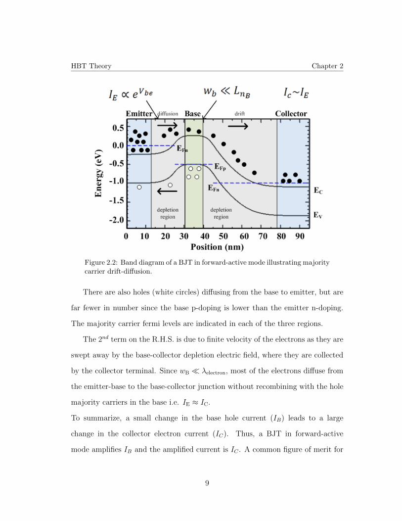
Figure 2.2 shows the band diagram of a BJT in forward-active mode with
electrons and holes drawn for illustrative purposes only. The number of electrons
(black circles) diffusing from the emitter to base drops off exponentially with the
conduction barrier height along the emitter-base junction (2.1).
nx=0 = nemitter exp(q(VBE − Vbi)
KT) (2.1)
The electrons then diffuse towards the base-collector junction. Since the base
thickness (wB) is much smaller than the electron diffusion length in the base (λe),
the diffusion profile is given by Eqn 2.2.
nx = nx=0(1− x
wB
) +JC
qvs
x
wB
(2.2)
8
HBT Theory Chapter 2
Figure 2.2: Band diagram of a BJT in forward-active mode illustrating majoritycarrier drift-diffusion.
There are also holes (white circles) diffusing from the base to emitter, but are
far fewer in number since the base p-doping is lower than the emitter n-doping.
The majority carrier fermi levels are indicated in each of the three regions.
The 2nd term on the R.H.S. is due to finite velocity of the electrons as they are
swept away by the base-collector depletion electric field, where they are collected
by the collector terminal. Since wB λelectron, most of the electrons diffuse from
the emitter-base to the base-collector junction without recombining with the hole
majority carriers in the base i.e. IE ≈ IC.
To summarize, a small change in the base hole current (IB) leads to a large
change in the collector electron current (IC). Thus, a BJT in forward-active
mode amplifies IB and the amplified current is IC . A common figure of merit for
9

HBT Theory Chapter 2
a BJT is the DC current gain β which is defined as:
β =IC
IB
=IE − IB
IB
(2.3)
The base current (IB) consists of holes that recombine with electrons diffusing
along the base, as well as holes diffusing in to the emitter. The latter hole diffusion
current is a parasitic current, and is thus undesirable. A Hetero-junction Bipolar
Junction Transistor (HBT) can be used to suppress this hole diffusion current,
by increasing the barrier for holes diffusing from the base to emitter. Thus, β
for the device increases exponentially as this barrier increases. Figure 2.3 shows
the band diagram of an HBT with an abrupt hetero-junction at the emitter-base
interface under forward-active mode. Note that while the hole diffusion barrier
has increased by 4EV, there is no change in the electron diffusion barrier as they
diffuse from emitter to base. For this design, β increases by exp(4EV).
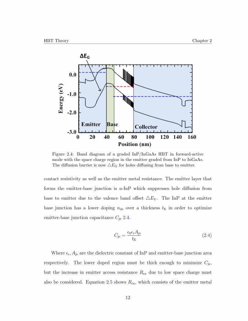
Figure 2.4 shows an HBT with an alloy grade between the emitter-base in-
terface. In this case, the hole diffusion barrier has increased by 4EG, and β by
exp(4EG).
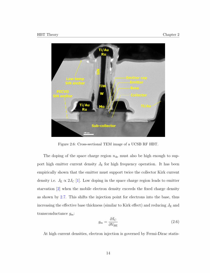
Figures 2.5, 2.6 show a cross-sectional schematic and TEM image respec-
tively of a UCSB RF HBT.
The emitter metal must maintain a high aspect ratio to maximize distance
between the metal plane and the transistor and thus ensure a clean RF environ-
ment. As mentioned in 2.1.3, the gap between the base metal and emitter-base
junction is minimized in order to reduce Rbb, and the base mesa is undercut in
order to reduce CCB.
10

HBT Theory Chapter 2
Figure 2.3: Band diagram of an abrupt InP/InGaAs HBT in forward-activemode. There exists a diffusion barrier 4EV for holes diffusing from base toemitter.
Sections 2.1.2 - 2.1.4 discuss the epitaxial and structural design of the device
in further detail.
2.1.2 HBT Emitter Design
A modern RF HBT emitter epitaxial design is shown in Table 2.1.
Layer Semiconductor Thickness (A) Doping (cm−3)Emitter cap In0.53Ga0.47As 100 8× 10¹⁹:Si
Emitter InP 150 5× 10¹⁹:SiEmitter InP 150 3× 10¹⁸:Si
Table 2.1: Typical emitter epi design of an RF HBT at wE of 100nm.
The top most layer of the emitter is highly doped n-InGaAs for obtaining low
contact resistivity. The emitter access resistance Rex includes the emitter metal
11
HBT Theory Chapter 2
Figure 2.4: Band diagram of a graded InP/InGaAs HBT in forward-activemode with the space charge region in the emitter graded from InP to InGaAs.The diffusion barrier is now 4EG for holes diffusing from base to emitter.
contact resistivity as well as the emitter metal resistance. The emitter layer that
forms the emitter-base junction is n-InP which suppresses hole diffusion from
base to emitter due to the valence band offset 4EV. The InP at the emitter
base junction has a lower doping nde over a thickness tE in order to optimize
emitter-base junction capacitance Cje 2.4.
Cje =ε0εrAje
tE(2.4)
Where εr, Aje are the dielectric constant of InP and emitter-base junction area
respectively. The lower doped region must be thick enough to minimize Cje,
but the increase in emitter access resistance Rex due to low space charge must
also be considered. Equation 2.5 shows Rex, which consists of the emitter metal
12

HBT Theory Chapter 2
Figure 2.5: Cross-sectional schematic of a UCSB RF HBT.
resistance, contact resistance, and emitter space charge resistance due to the lower
doped space charge layer.
Rex = Rem,metal +Rem,cont +Rem,sc
Rex = Rsh,em,metalT 2
em,metal
Aec
+ρem
Aec
+1
q
∂4Efn
∂IE
(2.5)
Rsh,em,metal : Emitter metal sheet resistance
T 2em,metal : Emitter metal thickness
Aec : Emitter contact area
ρem : Emitter contact resistivity
4Efn : Drop in electron quasi-Fermi level
4Efn =∫
tdep
JEµn(z)n(z)
dz
13
HBT Theory Chapter 2
Figure 2.6: Cross-sectional TEM image of a UCSB RF HBT.
The doping of the space charge region nde must also be high enough to sup-
port high emitter current density JE for high frequency operation. It has been
empirically shown that the emitter must support twice the collector Kirk current
density i.e. JE ∝ 2JC [1]. Low doping in the space charge region leads to emitter
starvation [2] when the mobile electron density exceeds the fixed charge density
as shown by 2.7. This shifts the injection point for electrons into the base, thus
increasing the effective base thickness (similar to Kirk effect) and reducing JE and
transconductance gm:
gm =∂IC
∂VBE
(2.6)
At high current densities, electron injection is governed by Fermi-Dirac statis-
14

HBT Theory Chapter 2
Figure 2.7: Band diagram of the emitter region at increasing emitter-basebiases. Emitter starvation occurs at sufficiently high JE [1].
tics and not Boltzmann statistics. Due to this, JE no longer increases exponen-
tially with Vbe, and now has a quadratic dependence. This further leads to gm
degradation [3].
2.1.3 HBT Base Design
A traditional UCSB RF HBT base epitaxial design is shown in Figure 2.2.
Layer Semiconductor Thickness (A) Doping (cm−3)Base In0.53Ga0.47As 300 9− 5× 10¹⁹:C
Table 2.2: Typical base epi design of an RF HBT at wE of 100nm.
The base employs a doping grade, where the highest doping is at the emitter-
base junction and the lowest at the base-collector. This induces a quasi-electric
field that accelerates electrons towards the base, thus reducing base transit time
15

HBT Theory Chapter 2
(τb) and minimizing electron-hole recombination in the base. The base transit
time τb must be computed based on the drift-diffusion model and is given by:
τB =T 2
B
Dn
kT
∆EC
[1− kT
∆EC
(1− exp(−∆EC
kT))] +
TB
vexit
kT
∆EC
(1− exp(∆EC
kT)) (2.7)
This quasi electric field also drives electrons away from the base surface, thus
reducing the number of electrons diffusing towards the base contact (Section 2.3.3).
This further increases β.
Experimentally, it has been determined that high base doping is required for
low ohmic contact resistivity [4] [5]. Thus, it is important for p-InGaAs doping
near the emitter-base junction to be as high as possible. Unfortunately, this leads
to β degradation due to increased Auger recombination, which is described in
further detail in section 2.3.2.
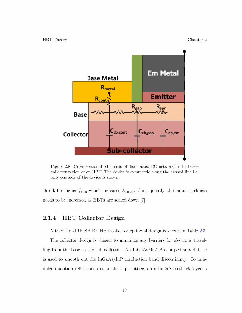
The base access resistance (Rbb) components are explained pictorially in Figure
2.8 and the corresponding equation is shown in Equation 2.8.
Rbb ≈ Rbe,spread +Rgap +Rb,cont. +Rb,metal
=Rsh,emWE
12LE
+Rsh,gapWgap
2LE
+
√Rsh,B,cont.ρB,cont.
2LE
coth(WB,cont.
LT
) + ρmetalWbc
6LE
.
(2.8)
The space charge resistance in the base Rgap is dependent on the base sheet
resistance and the gap between the emitter-base junction and base metal contact.
In RF HBTs, the emitter width has been reduced to 100nm and the gap spacing
to 10nm [6] such that Rgap is increasingly becoming a smaller portion of Rbb [7].
HBT scaling laws (Section 2.2) require that the base metal width wmetal,bc also
16
HBT Theory Chapter 2
Figure 2.8: Cross-sectional schematic of distributed RC network in the base–collector region of an HBT. The device is symmetric along the dashed line i.e.only one side of the device is shown.
shrink for higher fmax which increases Rmetal. Consequently, the metal thickness
needs to be increased as HBTs are scaled down [7].
2.1.4 HBT Collector Design
A traditional UCSB RF HBT collector epitaxial design is shown in Table 2.3.
The collector design is chosen to minimize any barriers for electrons travel-
ling from the base to the sub-collector. An InGaAs/InAlAs chirped superlattice
is used to smooth out the InGaAs/InP conduction band discontinuity. To min-
imize quantum reflections due to the superlattice, an n-InGaAs setback layer is
17

HBT Theory Chapter 2
Layer Semiconductor Thickness (A) Doping (cm−3)Setback In0.53Ga0.47As 95 1× 10¹⁷:Si
B-C grade - 120 1× 10¹⁷:Siδ-doping InP 30 5× 10¹⁸:SiCollector InP 455 1× 10¹⁷:Si
Sub-collector InP 75 2× 10¹⁹:SiSub-collector In0.53Ga0.47As 75 4× 10¹⁹:SiSub-collector InP 3000 1× 10¹⁹:Si
Etch stop In0.53Ga0.47As 35 undopedSubstrate InP - undoped
Table 2.3: Typical collector epi design of an RF HBT at wE of 100nm.
introduced before it to increase the electrons kinetic energy. The superlattice in-
troduced a quasi-electric field which is countered by a pulse doping after it on the
collector side [8].
The collector doping needs to be low, such that it is fully depleted in forward
active mode with zero base-collector bias. This minimizes base-collector capaci-
tance Ccb by maximizing space-charge width, and also minimizes change in Ccb
as Vcb is modulated. Figure 2.8 shows a physical interpretation of Ccb.
The collector doping also needs to be high enough to support a desired Kirk col-
lector current density JKirk,c i.e. the collector current density when the electric
field at the base side of the collector is zero (Equation 2.9) [9].
JC,Kirk = qnCve,sat (2.9)
Where nC, ve,sat are the collector electron concentration and saturation velocity
respectively.
The transit time for electrons traveling across the collector in the Kirk regime is
given by Equation 2.10, since they traverse the majority of the collector without
18
HBT Theory Chapter 2
scattering due to a large Γ− L separation [10] [11].
τC =∆QC
∆IC
=
∫ TC
0
1− x/TC
v(x)dx =
TC
2veff.
, (2.10)
As the collector is designed for higher JKirk,c and consequently higher ft, the
collector thickness Tc must decrease to ensure total depletion and this reduces the
device breakdown voltage Vce. Thus, there is a fundamental trade-off between
cutoff frequency and breakdown voltage.
The collector access resistance Rcc includes the collector contact resistance
Rc,contact, the lateral resistance between the base-collector mesa and the collector
contact Rc,gap and the spreading resistance in the intrinsic region under the base-
collector mesa Rc,intrinsic. Thus, Rcc is
RCC ≈ RC,intrinsic +RC,gap +RC,cont.
=Rsh,CWmesa
12LE
+Rsh,CWC,gap
2LE
+ρC,cont.
2LtLe
(2.11)
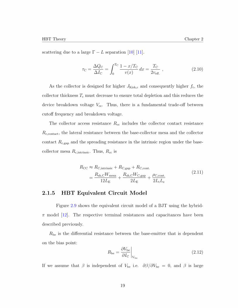
2.1.5 HBT Equivalent Circuit Model
Figure 2.9 shows the equivalent circuit model of a BJT using the hybrid-
π model [12]. The respective terminal resistances and capacitances have been
described previously.
Rbe is the differential resistance between the base-emitter that is dependent
on the bias point:
Rbe =∂Vbe
∂IC
∣∣∣∣Vbe
(2.12)
If we assume that β is independent of Vbe i.e. ∂β/∂Vbe = 0, and β is large
19
HBT Theory Chapter 2
Figure 2.9: Hybrid-π equivalent circuit model of a BJT.
enough that the emitter and collector currents are approximately equal, then the
resistance can be re-written as:
Rbe =β
gm
(2.13)
There exists an additional capacitance Cdiff at the base-emitter junction due
to carrier charge storage in forward bias.
Cdiff =∂IE
∂Vbe
(τb + τc) = gm(τb + τc) (2.14)
Rcb is associated with the base-collector junction, and is used to accurately fit
Y21 from s parameter measurements [7].
20
HBT Theory Chapter 2
2.2 HBT RF Performance and Scaling
The two important figures of merit for evaluating the RF performance
of HBTs are the current gain cut-off frequency ft, and the power gain cut-off
frequency fmax. ft is the frequency at which the current gain of the device drops
below unity i.e. the time it takes for an electron to travel from the emitter to the
collector. ft is given by:
1
2πfτ= τEC = τB + τB +
ηkT
qIE
Cje + (REX +RC +ηkT
qIE
)CCB , (2.15)
fmax is the frequency at which the unilateral Mason’s gain becomes unity i.e. it
is the maximum frequency of oscillation in a circuit where only only active device
is present [13]. It is given by:
fmax =
√fτ
8π(RC)eff.(2.16)
In order to increase the ft/fmax of a transistor, the time delays (τb, τc) must
be reduced by shrinking the device vertically, and the RC charging delays must
be reduced by shrinking the device laterally and reducing access resistances. To
first order, the scaling laws for various HBT design parameters are listed in table
2.4 for increasing RF performance.
The base contact resistivity is related to the base doping such that ρB,cont. ∝
N−2/3A,cont. as the doping levels are highly degenerate [14] [4].
Using these scaling laws, it is possible to make a scaling roadmap for HBTs, that
lists the specific design parameters required in a device for achieving certain RF
21

HBT Theory Chapter 2
Parameters Requirement
Base thickness TB γ−1/2
Collector thickness TC γ−1
B-C mesa width WBM γ−2
B-E junction width WE γ−2
Emitter current density JE γ2
Specific emitter contact resistivity ρE,cont. γ−2
Specific base contact resistivity ρB,cont. ≈ γ−2
Base sheet resistance RB,sh. γ−1/2
Base doping under contact NA,cont. γ3
Table 2.4: Scaling laws of HBTs: the required change for improving fτ andfmax by a factor of γ.
performance [15]. Such a roadmap is shown in figure 2.10.
Figure 2.10: Scaling roadmap for InP/InGaAs HBTs [15]
The primary challenges faced in achieving higher RF performance in HBTs
today are development of process flows for narrower emitter widths, and achieving
low base contact resistance to p-InGaAs [1] [16] [7] [4]. Section 2.4 provides a brief
outline of the work done at UCSB for achieving low base contact resistivity, and
details the problems associated with the current technology.
22

HBT Theory Chapter 2
Furthermore, it has been shown experimentally, and verified via simulations
that the DC current gain β drops as HBT emitter widths are scaled down for
higher RF performance [18]. Although not listed in the roadmap above, an HBT
requires high β in order to be used in power amplifiers, digital-analog converters,
and mixers. The following section details the factors that degrade β, as shown
by [16] and explores the design space for improving β.
2.3 DC Current Gain β
It has been observed experimentally that β decreases as the emitter width
is scaled down. Figure 2.11 shows this [16].
Figure 2.11: HBT DC current gain β plotted as a function of emitter perime-ter/area. Experimental and simulated data points show a drop in β as theemitter width is reduced. [16]
A decrease in β implies an increase in IB/IE as the emitter width is scaled. It
23

HBT Theory Chapter 2
is instructive to look at the relation between β and the base current components
as:
1
β∝ (ISRH + IRad + IAuger + IDiff + Isrf,cond + Isrf,rec)
∝ (1
βSRH+
1
βRad+
1
βAuger+
1
βDiff+
1
βsrf,cond+
1
βsrf,rec)−1
(2.17)
Figure 2.12 shows the various base current components. The physical explana-
tion for the current components and their respective scaling factors are discussed
in the following sub-sections, as well potential methods of decreasing them and
increasing β.
Figure 2.12: A cross-sectional schematic of an HBT that shows the various basecurrent components.
24

HBT Theory Chapter 2
2.3.1 Schockley-Read-Hall and Radiative Recombination
Current (ISRH,Irad)
As the electrons traverse the base, they recombine with the hole majority
carriers base on Shockley-Read-Hall (SRH) statistics [19]. The rate of recombina-
tion for the carriers is given by:
RSRH = CSRH(np− ni2) (2.18)
where ni is the intrinsic carrier concentration, and CSRH is the SRH recombination
coefficient.
It is clear that RSRH increases for HBTs designed for higher cut-off frequencies
(Table 2.5, 2.4), but the area of recombination decreases due to lateral and verti-
cal scaling.
Since InGaAs is a direct bandgap semiconductor, the electrons can also able to
recombine directly with a hole and emit photons. The radiative recombination
rate has a similar expression to 2.18, except that CSRH is replaced by Crad [16].
2.3.2 Auger Recombination Current (IAuger)
Auger recombination is a recombination process involving three or more
states in the in the conduction and valence band. The process in InGaAs is
depicted in Figure 2.13 [20].
It has been shown by [21] that the Auger recombination rate can be written
25
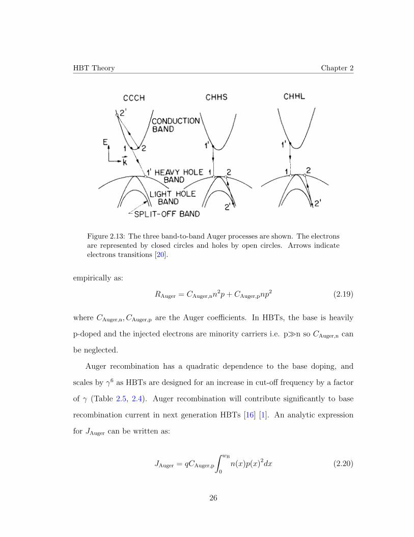
HBT Theory Chapter 2
Figure 2.13: The three band-to-band Auger processes are shown. The electronsare represented by closed circles and holes by open circles. Arrows indicateelectrons transitions [20].
empirically as:
RAuger = CAuger,nn2p+ CAuger,pnp
2 (2.19)
where CAuger,n, CAuger,p are the Auger coefficients. In HBTs, the base is heavily
p-doped and the injected electrons are minority carriers i.e. pn so CAuger,n can
be neglected.
Auger recombination has a quadratic dependence to the base doping, and
scales by γ6 as HBTs are designed for an increase in cut-off frequency by a factor
of γ (Table 2.5, 2.4). Auger recombination will contribute significantly to base
recombination current in next generation HBTs [16] [1]. An analytic expression
for JAuger can be written as:
JAuger = qCAuger,p
∫0
wB
n(x)p(x)2dx (2.20)
26

HBT Theory Chapter 2
For a doping graded base with a quasi-electric field 4EC, the electron concen-
tration at any given point in the base based on the drift-diffusion model is:
n(x) =kTwB
4EC
[−Jn
qDn
+ (−Jn
qDn
+4ECn(wB)
kTwB
)e−4ECkTwB
(wB−x)] (2.21)
The hole concentration at any point is given by the base doping at that point,
and can thus be engineered during growth. [1] explores different base design for re-
ducing Auger recombination while maintaining a high base doping at the emitter-
base junction for low base contact resistivity. Section 4.3 improves upon this
to further reduce Auger recombination in the base while maintaining low base
contact resistivity.
2.3.3 Lateral Diffusion Current (IDiff)
The electron carrier profile in the base as they travel to the collector can
be computed using Equation 2.21. However this does not take in to account the
electrons that diffuse laterally towards the base contact. [18] shows that IDiff is
highest in the gap between the base-emitter junction and the base metal contact,
and negligible everywhere else. Thus, IDiff scales with the emitter periphery.
Since IDiff is dominated by edge electrons, it increases as the emitter current den-
sity JE is increased for faster cut-off frequency (Table 2.5, 2.4).
The doping grade induced quasi-electric field accelerates electrons away from the
base surface and reduces IDiff . IDiff is also inversely proportional to the gap spac-
ing between base-emitter junction and base metal as that decreases the diffusion
profile slope. While the base doping grade and gap spacing can be increased to
27

HBT Theory Chapter 2
suppress Rbase,sh, it may also lead to higher base sheet resistance and higher Rbb.
2.3.4 Surface Recombination and Conduction Current
(Isrf,rec, Isrf,cond)
The surface gap region in the base contains donor-like trap states that
carry positive charge when they capture holes [22]. This charge pins the surface
Fermi level of InGaAs at 0.5 eV below the conduction band, and thus induces a
depletion region that acts as a channel for electrons traveling from base-emitter
junction to base metal [18]. The electrons at the surface can also recombine with
the surface states, generating surface recombination current Isrf,rec:
Isrf,SRH = qns(x)vsrf,rec (2.22)
where vsrf,rec is the surface recombination velocity of electrons. The density of
trapped electrons ns depends on JE, field in the surface depletion region, surface
depletion depth, and the scattering function that scatters electrons into the surface
channel.
The surface currents Isrf,cond, Isrf,rec can be decreased by increasing surface base
doping and thus decreasing surface depletion depth. Decreasing the surface trap
state density via surface passivation would also reduce the surface currents [23]
[24].
28
HBT Theory Chapter 2
2.3.5 DC Current Gain β with HBT Scaling
As emitter width is scaled and base doping increased for higher RF perfor-
mance, β decreases as the edge base current components do not decrease in pro-
portion to the emitter current, and the IAuger increase is quadratic with the base
doping.
Table 2.5 shows the scaling laws for these current components as a function of
emitter and base mesa width, base doping, and base thickness as devices are scaled
for an increase in cut-off frequencies by a factor of γ.
Parameters Scaling RequirementScaling Effect On Current ComponentsIB,Bulk IB,Diff IB,Srf IB,Auger
PE/AE ≈ 1/wE γ−2 γ−2 γ0 γ0 γ−2
PBM/ABM γ−2 γ0 γ0 γ0 γ0
JE γ2 γ2 γ2 ≈γ2 ≈γ2
NA γ3 γ3 γ0 - γ6
TB γ−1 γ−1 γ0 γ0 γ−1
Table 2.5: Scaling effect on base current components, as a function of parameterscaling for an increase in fτ and fmax by a factor of γ. No current spreadingin the base, and a uniformly doped base is assumed.
From the table, it is clear that the base current does not decrease proportion-
ally as the emitter width is scaled for faster cut-off frequencies. Section 3.4 and 4
discuss ways in which β can be increased.
2.4 Base Contact Technology
As discussed in Section 2.2, achieving low base contact resistivity for high RF
performance is currently one of the biggest challenges. At UCSB, various base
contact technologies have been developed previously, each with their own pros and
cons. This section summarizes the work done previously. The limitations of these
29
HBT Theory Chapter 2
technologies is used as a motivation for a part of this dissertation and is discussed
in chapter 4.
2.4.1 Lift-Off Pt/Ti/Pd/Au Contacts
Lift-Off Pt or Pd contacts are common in InGaAs devices [25] [5], as they
yield contact resistivities < 100Ω.µm2 on p-InGaAs at > 1019cm−3 doping [4].
Figure 2.14 shows a cross-sectional TEM image of an HBT with lifted off
Pt/Ti/Pd/Au contacts [26].
This technology has the advantage that it requires minimal number of fabrica-
tion steps, and uses chemically inert metals that are not attacked by subsequent
process chemistry.
However, Pt reacts/diffuses with p-InGaAs [27] and thus the top 6 nm of the
base is consumed by metal. The metal no longer contacts the highest doping
p-InGaAs as the base has a linear doping grade from the emitter to collector side.
Furthermore, lift-off technology introduces photoresist contamination on the p-
InGaAs surface which increases base contact resistivity [7].
2.4.2 Refractory Metal Contacts
Surface contamination of the base surface can be minimized by blanket
deposition of the base contact metal as soon as the emitter semiconductor is
etched away. Furthermore, a refractory metal contact can be used to minimize
metal reaction and sinking into the base semiconductor. Previous work has shown
that blanket refractory metal contacts can be used to obtain <1 Ω.µm2 contact
resistivities on test structures [28]. Figure 2.15 shows a cross-sectional TEM of an
30

HBT Theory Chapter 2
Figure 2.14: A cross-sectional TEM image shows the Pt/Ti/Au base contactsinking into the p-InGaAs base. [16].
RF HBT with a ruthenium base contact. It can be seen that there is no discernible
sinking of the metal contact into the InGaAs base. Ti/Au metal pads were lifted
off in subsequent steps.
However, it has not been possible to reproduce low contact resistivity on RF
HBTs [7]. Section 3.2 details some work that has been done on refractory base
contact technology.
31

HBT Theory Chapter 2
Figure 2.15: A cross-sectional TEM image shows the Ru/Ti/Au base contactwith no discernible metal sinking. [7].
2.4.3 Blanket Pt/Ru Metal Contacts
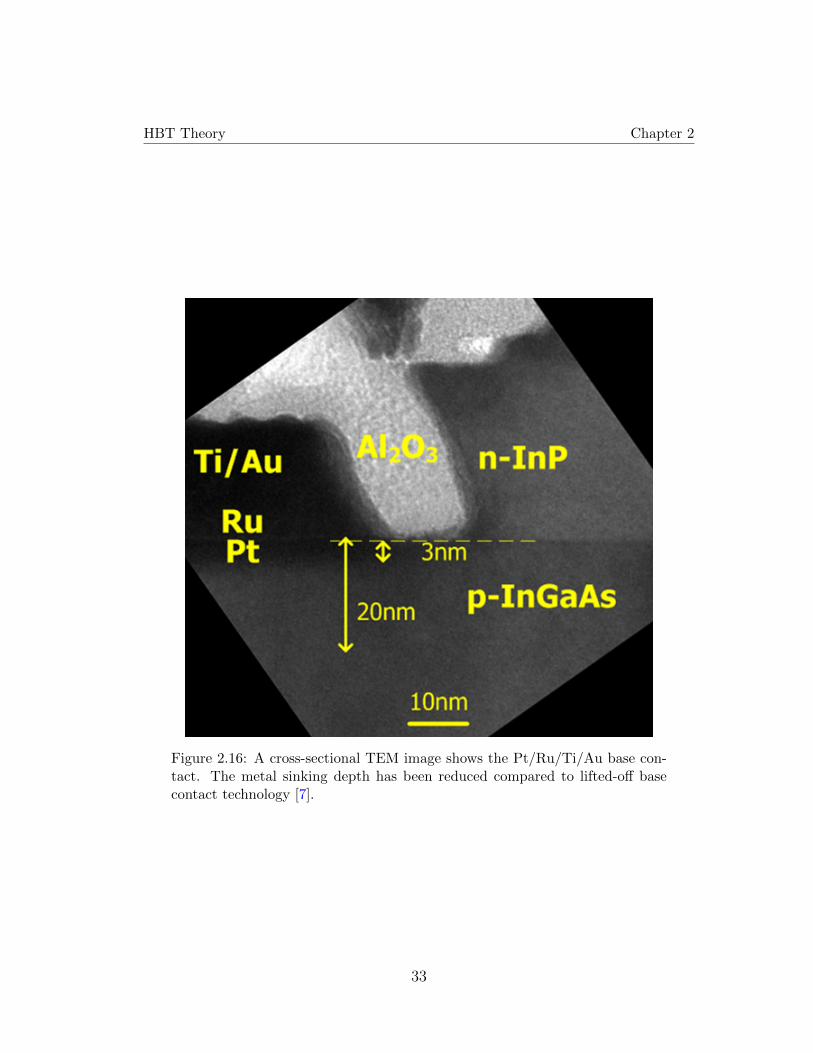
[6] [7] show a blanket base metal contact that uses Pt as the contact metal,
and Ru as a refractory metal barrier above it to prevent Ti diffusion into the base.
Figure 2.16 shows a cross-sectional TEM of such an RF HBT.
It has been possible to achieve contact resistivity of 3 Ω.µm2 on RF HBTs
using blanket Pt/Ru contacts. However, the technology still suffers from contact
metal sinking, although the sinking depth has been reduced compared to lifted-off
Pt/Ti/Pd/Au contacts.
32
HBT Theory Chapter 2
Figure 2.16: A cross-sectional TEM image shows the Pt/Ru/Ti/Au base con-tact. The metal sinking depth has been reduced compared to lifted-off basecontact technology [7].
33
REFERENCES
References
[1] V. Jain, InP DHBTs in a Refractory Emitter Process for THz Electronics..Ph.D. Thesis, University of California, Santa Barbara, Santa. Barbara, Ca,U.S.A., 2011.
[2] Rodwell, Mark J.W.; Urteaga, M.; Mathew, T.; Scott, D.; Mensa, Dino; Lee,Q.; Guthrie, J.; Betser, Y.; Martin, S.C.; Smith, R.P.; Jaganathan, S.; Kr-ishnan, S.; Long, S.I.; Pullela, R.; Agarwal, B.; Bhattacharya, U.; Samoska,L.; Dahlstrom, M., ”Submicron scaling of HBTs,” in Electron Devices, IEEETransactions on , vol.48, no.11, pp.2606-2624, Nov 2001
[3] Jain, V.; Rodwell, Mark J.W., ”Transconductance Degradation inNear-THz InP Double-Heterojunction Bipolar Transistors,” in ElectronDevice Letters, IEEE , vol.32, no.8, pp.1068-1070, Aug. 2011. doi:10.1109/LED.2011.2157451
[4] A. Baraskar, A. C. Gossard, and M. J. W. Rodwell, “Lower limits tometal-semiconductor contact resistance: Theoretical models and experimen-tal data,” J. Appl. Phys., vol. 114, p. 154516, Oct. 2013.
[5] J. Lin, S. Yu, and S. Mohney, ”Characterization of low-resistance ohmiccontacts to n-and p-type InGaAs,” Journal of Applied Physics, vol. 114, no.4, p. 044504, 2013.
[6] Rode, J.C.; Chiang, H.-W.; Choudhary, P.; Jain, V.; Thibeault, B.J.;Mitchell, W.J.; Rodwell, M.J.W.; Urteaga, M.; Loubychev, D.; Snyder, A.;Wu, Y.; Fastenau, J.M.; Liu, A.W.K., ”An InGaAs/InP DHBT With Simul-taneous ft/fmax 404/901 GHz and 4.3 V Breakdown Voltage,” in ElectronDevices Society, IEEE Journal of the , vol.3, no.1, pp.54-57, Jan. 2015
[7] J. Rode, IC Fabrication Technology for Highly Scaled THz DHBTs.. Ph.D.Thesis, University of California, Santa Barbara, Santa. Barbara, Ca, U.S.A.,2015.
[8] Z. Griffith, Ultra High Speed InGaAs / InP DHBT Devices and Circuits..Ph.D. Thesis, University of California, Santa Barbara, Santa. Barbara, Ca,U.S.A., 2005.
[9] Kirk, C.T., Jr., ”A theory of transistor cutoff frequency (fT) falloff at highcurrent densities,” in Electron Devices, IRE Transactions on , vol.9, no.2,pp.164-174, March 1962
34

REFERENCES
[10] T. Ishibashi, Influence of electron velocity overshoot on collector transit.times of HBTs, Electron Devices, IEEE Transactions on, vol. 37, pp. 2103.2105, Sep. 1990.
[11] S. Laux and W. Lee, Collector signal delay in the presence of velocity over-shoot, Electron Device Letters, IEEE, vol. 11, pp. 174176, Apr. 1990.
[12] Giacoletto, L.J., ”Diode and transistor equivalent circuits for transient oper-ation,” in Solid-State Circuits, IEEE Journal of , vol.4, no.2, pp.80-83, Apr1969
[13] Mason, S.J., ”Power Gain in Feedback Amplifier,” in Circuit Theory, Trans-actions of the IRE Professional Group on , vol.CT-1, no.2, pp.20-25, June1954
[14] Full band calculations of the intrinsic lower limit of contact resistivity.Maassen, J. and Jeong, C. and Baraskar, A. and Rodwell, M. and Lund-strom, M., Applied Physics Letters, 102, 111605 (2013)
[15] M. J. W. Rodwell, M. Le, and B. Brar, “InP Bipolar ICs: Scaling Roadmaps,.Frequency Limits, Manufacturable Technologies,” Proc. IEEE, vol. 92,.pp. 271–286, Feb. 2008.
[16] H. Chiang, Design and Fabrication of Sub-100nm Base-Emitter Junctionsof THz InP DHBTs.. Ph.D. Thesis, University of California, Santa Barbara,Santa Barbara, Ca, U.S.A., 2014...
[17] . Lateral carrier diffusion and current gain in terahertz InGaAs/InP double-heterojunction bipolar transistors. Chiang, Han-Wei and Rode, Johann C.and Choudhary, Prateek and Rodwell, Mark J. W., Journal of AppliedPhysics, 115, 034513 (2014)
[18] Lateral carrier diffusion and current gain in terahertz InGaAs/InP double-heterojunction bipolar transistors. Chiang, Han-Wei and Rode, Johann C.and Choudhary, Prateek and Rodwell, Mark J. W., Journal of AppliedPhysics, 115, 034513 (2014)
[19] W. Shockley and W. T. Read, Jr., Statistics of the Recombinations of Holesand Electrons, Physical Review, vol. 87, pp. 835–841, Sep. 1952.
[20] N. K. Dutta and R. J. Nelson, The case for Auger recombination inIn1−xGaxAsyP1−y,” J. Appl. Phys., vol. 53, pp. 74–92, Jan. 1982.
35

REFERENCES
[21] L. A. Coldren and S. W. Corzine, Diode Lasers and Photonic IntegratedCircuits.. Wiley Series in Microwave abd Optical Engineering, 1995.
[22] H. Hasegawa, “Fermi Level Pinning and Schottky Barrier Height Control atMetal-Semiconductor Interfaces of InP and Related Materials,” Jpn. J. Appl.Phys., vol. 38, p. 10981102, Feb. 1999.
[23] C. L. Hinkle, M. Milojevic, B. Brennan, A. M. Sonnet, F. S. Aguirre-Tostado,G. J. Hughes, E. M. Vogel, and R. M. Wallace, “Detection of Ga suboxidesand their impact on III-V passivation and Fermi-level pinning,” Appl. Phys.Lett., vol. 94, p. 162101, Apr. 2009.
[24] V. Chobpattana, J. Son, J. J. M. Law, R. Engel-Herbert, C. Y. Huang, andS. Stemmer, “Nitrogen-passivated dielectric/InGaAs interfaces with sub-nmequivalent oxide thickness and low interface trap densities,” Appl. Phys.Lett., vol. 102, pp. 022907–1–022907–3, Jan. 2013.
[25] E. F. Chor, W. K. Chong, and C. H. Heng, “Alternative (Pd,Ti,Au) contactsto (Pt,Ti,Au) contacts for In0.53Ga0.47As,” J. Appl. Phys., vol. 84, pp. 2977–2979, Sep. 1998.
[26] Jain, V.; Rode, J.C.; Han-Wei Chiang; Baraskar, A.; Lobisser, E.; Thibeault,Brian J.; Rodwell, M.; Urteaga, M.; Loubychev, D.; Snyder, A.; Wu, Y.;Fastenau, J.M.; Liu, W.K., ”1.0 THz fmax InP DHBTs in a refractory emitterand self-aligned base process for reduced base access resistance,” in DeviceResearch Conference (DRC), 2011 69th Annual , vol., no., pp.271-272, 20-22June 2011
[27] Chor, E.F.; Malik, R.J.; Hamm, R.A.; Ryan, R., ”Metallurgical stability ofohmic contacts on thin base InP/InGaAs/InP HBT’s,” in Electron DeviceLetters, IEEE , vol.17, no.2, pp.62-64, Feb. 1996
[28] Ultralow resistance, nonalloyed Ohmic contacts to n-InGaAs Baraskar,Ashish K. and Wistey, Mark A. and Jain, Vibhor and Singisetti, Uttam andBurek, Greg and Thibeault, Brian J. and Lee, Yong Ju and Gossard, ArthurC. and Rodwell, Mark J. W., Journal of Vacuum Science and Technology B,27, 2036-2039 (2009)
36

Chapter 3
RF HBT Improvements
Next generation HBTs require improved process flows for further lateral scaling
of device dimensions, lower base contact resistivities, and higher β. This chapter
discusses work that has been done to improve the mentioned parameters. Im-
proved epitaxial designs for higher emitter current density JE and process flow
improvements for reduced thermal shock and increased yield are also discussed.
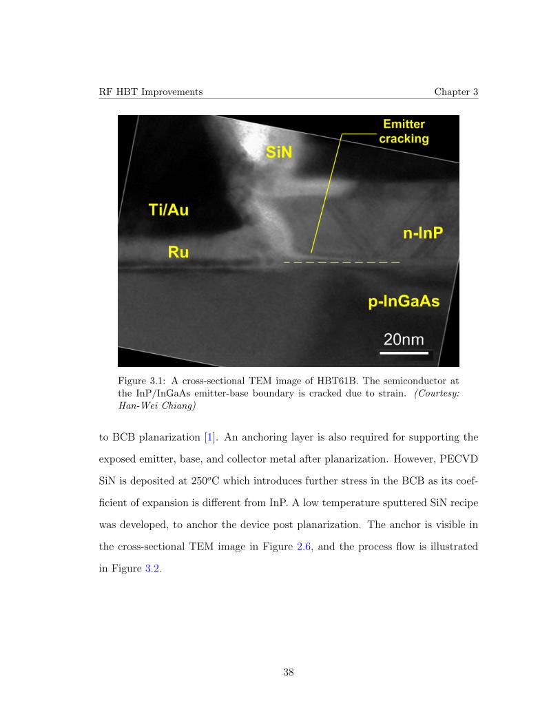
3.1 Reducing Thermal Shock For Improved Yield
As emitter widths are scaled to 100 nm, the high aspect ratio emitter metal
stack becomes sensitive to physical stress that is induced during fabrication. Shear
stress is introduced when the device is planarized using benzocyclobutene (BCB).
Figure 3.1 shows a cross-sectional TEM of an HBT where the emitter semicon-
ductor is cracking due to the added stress.
To increase structural support to the emitter metal stack, a 30 nm SiN layer
was deposited via Plasma Enhanced Chemical Vapour Deposition (PECVD) prior
37
RF HBT Improvements Chapter 3
Figure 3.1: A cross-sectional TEM image of HBT61B. The semiconductor atthe InP/InGaAs emitter-base boundary is cracked due to strain. (Courtesy:Han-Wei Chiang)
to BCB planarization [1]. An anchoring layer is also required for supporting the
exposed emitter, base, and collector metal after planarization. However, PECVD
SiN is deposited at 250oC which introduces further stress in the BCB as its coef-
ficient of expansion is different from InP. A low temperature sputtered SiN recipe
was developed, to anchor the device post planarization. The anchor is visible in
the cross-sectional TEM image in Figure 2.6, and the process flow is illustrated
in Figure 3.2.
38
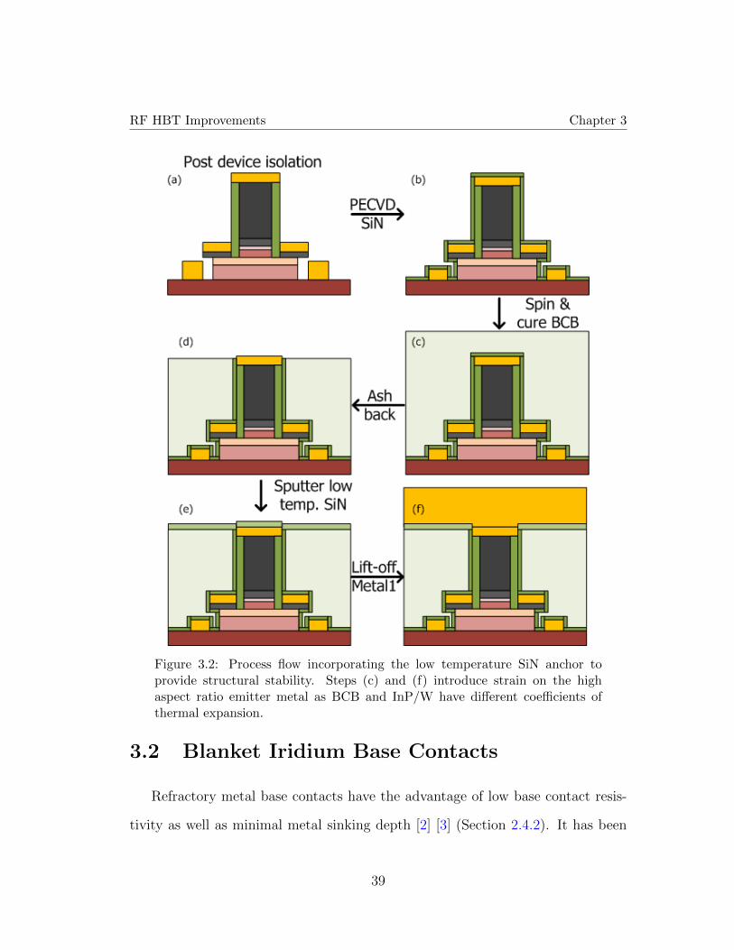
RF HBT Improvements Chapter 3
Figure 3.2: Process flow incorporating the low temperature SiN anchor toprovide structural stability. Steps (c) and (f) introduce strain on the highaspect ratio emitter metal as BCB and InP/W have different coefficients ofthermal expansion.
3.2 Blanket Iridium Base Contacts
Refractory metal base contacts have the advantage of low base contact resis-
tivity as well as minimal metal sinking depth [2] [3] (Section 2.4.2). It has been
39

RF HBT Improvements Chapter 3
shown on test structures previously that Iridium contacts to p-InGaAs yield sub-
Ω.µm2 contact resistivity at a doping of 2*1020cm−3 [3]. This section shows a
process flow that was developed for integrating Ir base contacts into an RF HBT
process.
The process for a refractory base contact metal requires blanket metal depo-
sition, and it must be etched away from the field prior to base mesa wet etch.
Iridium is the most corrosion resistant metal known [4], and thus requires a high
power SF6/Ar plasma etch to remove it from the field. Since this would also
attack the emitter metal and gap region between emitter and base metal, it is
important to protect them during etch. Figure 3.3 shows an angled SEM image
of HBT emitter metal and test structures that have been etched away due to
incomplete protection.
Figure 3.3: Angled SEM image of sample after Ir dry etch. The W/TiWemitter metal has been etched due to insufficient protection during the etch.(a) Emitter (b) Vernier test structures.
A dual sidewall process was developed, where blanket Al2O3 was deposited
via Atomic Layer Deposition (ALD) followed by blanket SiN via PECVD. The
SiN was subsequently etched using a CF4/O2 anisotropic dry etch to form a SiN
sidewall and the Al2O3 was wet etched using dilute HF to expose the Ir. The
40
RF HBT Improvements Chapter 3
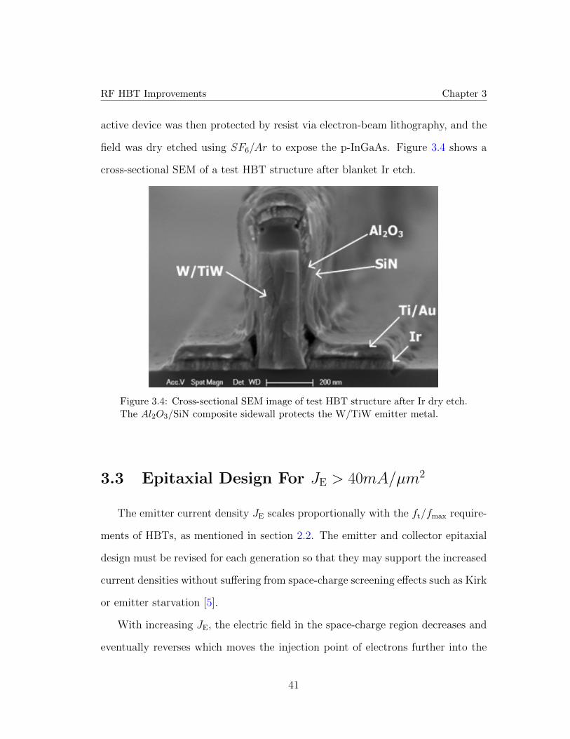
active device was then protected by resist via electron-beam lithography, and the
field was dry etched using SF6/Ar to expose the p-InGaAs. Figure 3.4 shows a
cross-sectional SEM of a test HBT structure after blanket Ir etch.
Figure 3.4: Cross-sectional SEM image of test HBT structure after Ir dry etch.The Al2O3/SiN composite sidewall protects the W/TiW emitter metal.
3.3 Epitaxial Design For JE > 40mA/µm2
The emitter current density JE scales proportionally with the ft/fmax require-
ments of HBTs, as mentioned in section 2.2. The emitter and collector epitaxial
design must be revised for each generation so that they may support the increased
current densities without suffering from space-charge screening effects such as Kirk
or emitter starvation [5].
With increasing JE, the electric field in the space-charge region decreases and
eventually reverses which moves the injection point of electrons further into the
41
RF HBT Improvements Chapter 3
emitter as shown in Figure 2.7. This increases the effective base width wB, and
also decreases JE as (4EFn −4EC) at the injection point goes down.
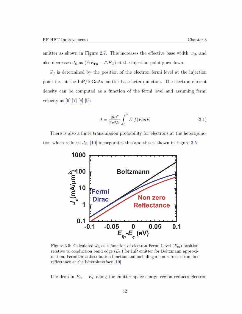
JE is determined by the position of the electron fermi level at the injection
point i.e. at the InP/InGaAs emitter-base heterojunction. The electron current
density can be computed as a function of the fermi level and assuming fermi
velocity as [6] [7] [8] [9]:
J =qm∗
2π2~3
∫0
∞
E.f(E)dE (3.1)
There is also a finite transmission probability for electrons at the heterojunc-
tion which reduces JE. [10] incorporates this and this is shown in Figure 3.5.
Figure 3.5: Calculated JE as a function of electron Fermi Level (Efn) positionrelative to conduction band edge (EC) for InP emitter for Boltzmann approxi-mation, FermiDirac distribution function and including a non-zero electron fluxreflectance at the heterointerface [10]
The drop in Efn − EC along the emitter space-charge region reduces electron
42

RF HBT Improvements Chapter 3
state density, and thus the space charge region must be optimized to reduce this
barrier. Based on Figure 3.5, an emitter current density of 40 mA/µ2 requires the
electron Fermi level Efn to be ≈0.85eV above the conduction band. The emitter
epitaxial design shown in Table 3.1 is designed for a maximum emitter current
density of 50 mA/µm2.
Layer Semiconductor Old/New Thickness (A) Old/New Doping (cm−3)Emitter cap In0.53Ga0.47As 100/100 8/8×1019:Si
Emitter InP 150/80 4/4×1019:SiEmitter InP 150/50 3/7×1019:Si
Table 3.1: Optimized emitter epi design for JE of 50 mA/µm2
The above analysis assumes zero change in the electron Fermi level Efn along
the space-charge region and also neglects barrier modulation effects [10]. Thus,
the maximum available JE may be lower.
It is important to note that this reduces the thickness of the InP layers, thus
the hole diffusion current from base to emitter is expected to increase due to a
steeper diffusion profile.
3.4 Reducing Auger Recombination
As discussed in section 2.3.2, Auger recombination in the base starts to be a
larger portion of the base current as the base doping increases, thus reducing β.
While the base doping must be lowered to reduce Auger recombination, it must be
high enough at the surface to yield low Rb,contact and have a low Rb,sh. [5] suggests
using a highly doped pulse layer at the emitter-base junction (Figure 3.6) which
reduces Rb,contact while maintaining low Auger recombination in the remainder of
43
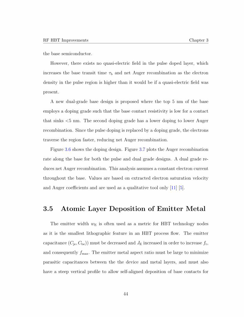
RF HBT Improvements Chapter 3
the base semiconductor.
However, there exists no quasi-electric field in the pulse doped layer, which
increases the base transit time τb and net Auger recombination as the electron
density in the pulse region is higher than it would be if a quasi-electric field was
present.
A new dual-grade base design is proposed where the top 5 nm of the base
employs a doping grade such that the base contact resistivity is low for a contact
that sinks <5 nm. The second doping grade has a lower doping to lower Auger
recombination. Since the pulse doping is replaced by a doping grade, the electrons
traverse the region faster, reducing net Auger recombination.
Figure 3.6 shows the doping design. Figure 3.7 plots the Auger recombination
rate along the base for both the pulse and dual grade designs. A dual grade re-
duces net Auger recombination. This analysis assumes a constant electron current
throughout the base. Values are based on extracted electron saturation velocity
and Auger coefficients and are used as a qualitative tool only [11] [5].
3.5 Atomic Layer Deposition of Emitter Metal
The emitter width wE is often used as a metric for HBT technology nodes
as it is the smallest lithographic feature in an HBT process flow. The emitter
capacitance (Cje, Cbe)) must be decreased and JE increased in order to increase ft,
and consequently fmax. The emitter metal aspect ratio must be large to minimize
parasitic capacitances between the the device and metal layers, and must also
have a steep vertical profile to allow self-aligned deposition of base contacts for
44
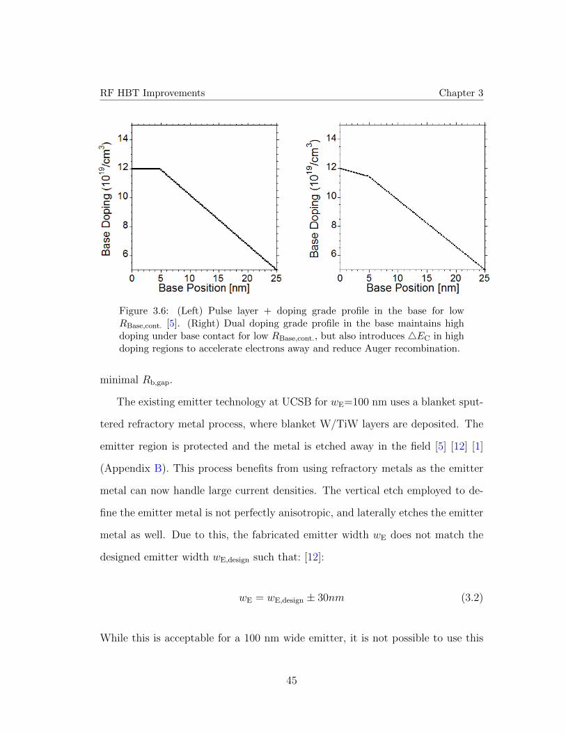
RF HBT Improvements Chapter 3
Figure 3.6: (Left) Pulse layer + doping grade profile in the base for lowRBase,cont. [5]. (Right) Dual doping grade profile in the base maintains highdoping under base contact for low RBase,cont., but also introduces 4EC in highdoping regions to accelerate electrons away and reduce Auger recombination.
minimal Rb,gap.
The existing emitter technology at UCSB for wE=100 nm uses a blanket sput-
tered refractory metal process, where blanket W/TiW layers are deposited. The
emitter region is protected and the metal is etched away in the field [5] [12] [1]
(Appendix B). This process benefits from using refractory metals as the emitter
metal can now handle large current densities. The vertical etch employed to de-
fine the emitter metal is not perfectly anisotropic, and laterally etches the emitter
metal as well. Due to this, the fabricated emitter width wE does not match the
designed emitter width wE,design such that: [12]:
wE = wE,design ± 30nm (3.2)
While this is acceptable for a 100 nm wide emitter, it is not possible to use this
45
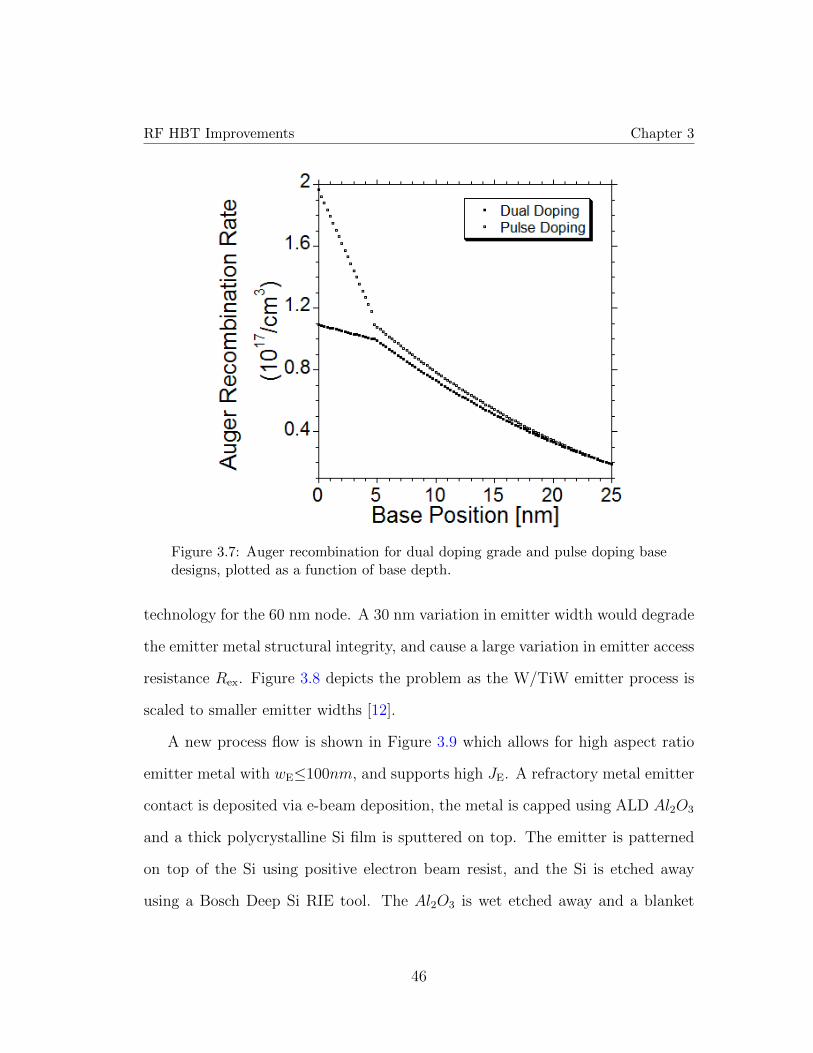
RF HBT Improvements Chapter 3
Figure 3.7: Auger recombination for dual doping grade and pulse doping basedesigns, plotted as a function of base depth.
technology for the 60 nm node. A 30 nm variation in emitter width would degrade
the emitter metal structural integrity, and cause a large variation in emitter access
resistance Rex. Figure 3.8 depicts the problem as the W/TiW emitter process is
scaled to smaller emitter widths [12].
A new process flow is shown in Figure 3.9 which allows for high aspect ratio
emitter metal with wE≤100nm, and supports high JE. A refractory metal emitter
contact is deposited via e-beam deposition, the metal is capped using ALD Al2O3
and a thick polycrystalline Si film is sputtered on top. The emitter is patterned
on top of the Si using positive electron beam resist, and the Si is etched away
using a Bosch Deep Si RIE tool. The Al2O3 is wet etched away and a blanket
46
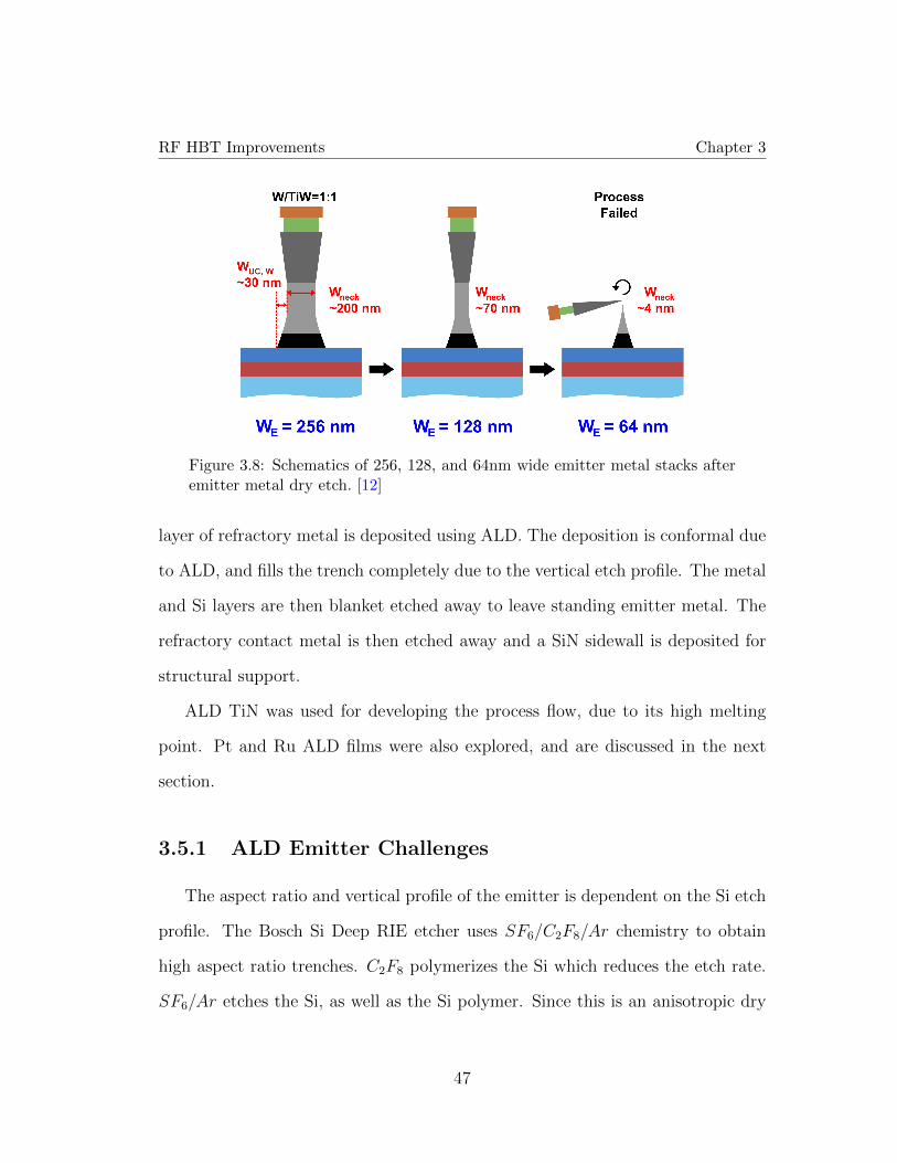
RF HBT Improvements Chapter 3
Figure 3.8: Schematics of 256, 128, and 64nm wide emitter metal stacks afteremitter metal dry etch. [12]
layer of refractory metal is deposited using ALD. The deposition is conformal due
to ALD, and fills the trench completely due to the vertical etch profile. The metal
and Si layers are then blanket etched away to leave standing emitter metal. The
refractory contact metal is then etched away and a SiN sidewall is deposited for
structural support.
ALD TiN was used for developing the process flow, due to its high melting
point. Pt and Ru ALD films were also explored, and are discussed in the next
section.
3.5.1 ALD Emitter Challenges
The aspect ratio and vertical profile of the emitter is dependent on the Si etch
profile. The Bosch Si Deep RIE etcher uses SF6/C2F8/Ar chemistry to obtain
high aspect ratio trenches. C2F8 polymerizes the Si which reduces the etch rate.
SF6/Ar etches the Si, as well as the Si polymer. Since this is an anisotropic dry
47
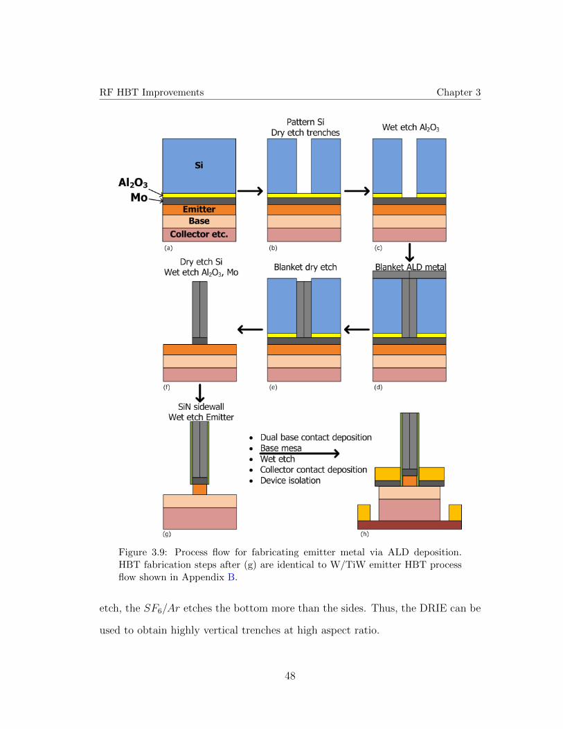
RF HBT Improvements Chapter 3
Figure 3.9: Process flow for fabricating emitter metal via ALD deposition.HBT fabrication steps after (g) are identical to W/TiW emitter HBT processflow shown in Appendix B.
etch, the SF6/Ar etches the bottom more than the sides. Thus, the DRIE can be
used to obtain highly vertical trenches at high aspect ratio.
48
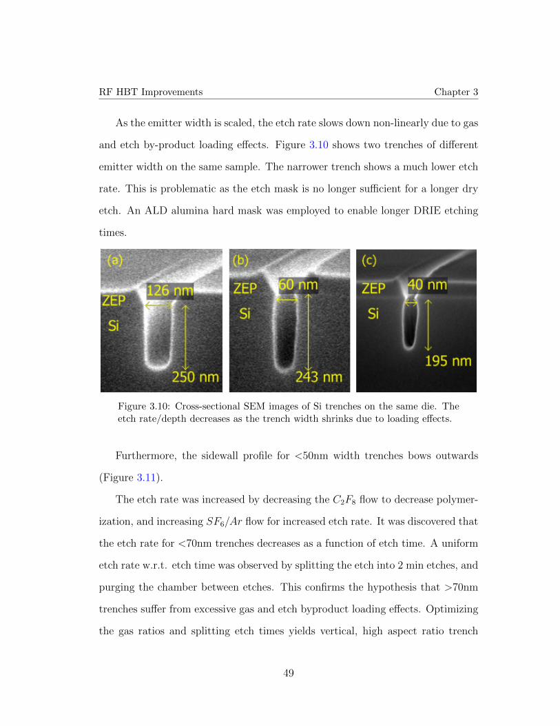
RF HBT Improvements Chapter 3
As the emitter width is scaled, the etch rate slows down non-linearly due to gas
and etch by-product loading effects. Figure 3.10 shows two trenches of different
emitter width on the same sample. The narrower trench shows a much lower etch
rate. This is problematic as the etch mask is no longer sufficient for a longer dry
etch. An ALD alumina hard mask was employed to enable longer DRIE etching
times.
Figure 3.10: Cross-sectional SEM images of Si trenches on the same die. Theetch rate/depth decreases as the trench width shrinks due to loading effects.
Furthermore, the sidewall profile for <50nm width trenches bows outwards
(Figure 3.11).
The etch rate was increased by decreasing the C2F8 flow to decrease polymer-
ization, and increasing SF6/Ar flow for increased etch rate. It was discovered that
the etch rate for <70nm trenches decreases as a function of etch time. A uniform
etch rate w.r.t. etch time was observed by splitting the etch into 2 min etches, and
purging the chamber between etches. This confirms the hypothesis that >70nm
trenches suffer from excessive gas and etch byproduct loading effects. Optimizing
the gas ratios and splitting etch times yields vertical, high aspect ratio trench
49

RF HBT Improvements Chapter 3
Figure 3.11: Cross-sectional SEM images of Si trenches that bows outwards inthe middle. This leads to a hollow ’teardrop’ when ALD TiN is deposited. Thedeposited TiN film thickness in the trench is nearly half of the thickness in thefield.
profiles as shown in Figure 3.12.
Figure 3.12: Cross-sectional SEM images of 70nm wide high aspect ratio Si trenches.
50
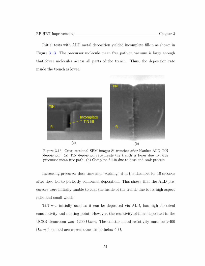
RF HBT Improvements Chapter 3
Initial tests with ALD metal deposition yielded incomplete fill-in as shown in
Figure 3.13. The precursor molecule mean free path in vacuum is large enough
that fewer molecules access all parts of the trench. Thus, the deposition rate
inside the trench is lower.
Figure 3.13: Cross-sectional SEM images Si trenches after blanket ALD TiNdeposition. (a) TiN deposition rate inside the trench is lower due to largeprecursor mean free path. (b) Complete fill-in due to dose and soak process.
Increasing precursor dose time and ”soaking” it in the chamber for 10 seconds
after dose led to perfectly conformal deposition. This shows that the ALD pre-
cursors were initially unable to coat the inside of the trench due to its high aspect
ratio and small width.
TiN was initially used as it can be deposited via ALD, has high electrical
conductivity and melting point. However, the resistivity of films deposited in the
UCSB cleanroom was 1200 Ω.nm. The emitter metal resistivity must be >400
Ω.nm for metal access resistance to be below 1 Ω.
51

RF HBT Improvements Chapter 3
ALD Pt was explored as an alternative due to its low resistivity of 40 Ω.nm,
and was successfully deposited on test structures. However, the blanket Si dry
etch also etches Pt. Figure 3.14 shows an angled SEM image of a Pt emitter
after the Si has been etched away in the field. A portion of the emitter has been
protected by Ti/Au and thus the full emitter cross-section is visible under it.
However, emitter metal outside of the capped region has been etched.
Figure 3.14: Angled SEM image of Pt emitter after blanket Si etch. The emitterregion exposed to Si etch has been attacked.
ALD Ru is reported to have low resistivity of 60Ω.nm [14], is etch resistant and
also has a high melting point. However, we were unable to develop this process
at UCSB as Ru requires chamber pressure of >750mT for precursor adhesion
and subsequent seed layer formation. The Oxford Instruments FlexAL Atomic
Layer Deposition system at UCSB is designed for a maximum chamber pressure
of 250mT only.
52
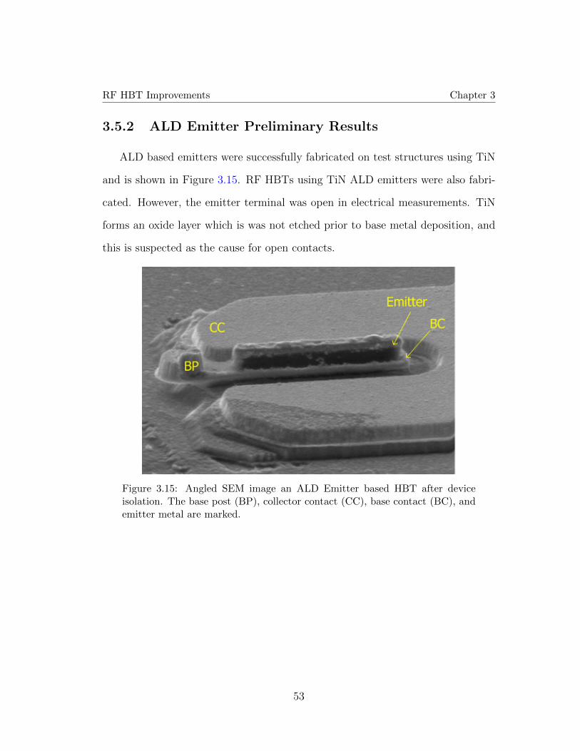
RF HBT Improvements Chapter 3
3.5.2 ALD Emitter Preliminary Results
ALD based emitters were successfully fabricated on test structures using TiN
and is shown in Figure 3.15. RF HBTs using TiN ALD emitters were also fabri-
cated. However, the emitter terminal was open in electrical measurements. TiN
forms an oxide layer which is was not etched prior to base metal deposition, and
this is suspected as the cause for open contacts.
Figure 3.15: Angled SEM image an ALD Emitter based HBT after deviceisolation. The base post (BP), collector contact (CC), base contact (BC), andemitter metal are marked.
53
REFERENCES
References
[1] J. Rode, IC Fabrication Technology for Highly Scaled THz DHBTs.. Ph.D.Thesis, University of California, Santa Barbara, Santa. Barbara, Ca, U.S.A.,2015.
[2] Ultralow resistance, nonalloyed Ohmic contacts to n-InGaAs Baraskar,Ashish K. and Wistey, Mark A. and Jain, Vibhor and Singisetti, Uttam andBurek, Greg and Thibeault, Brian J. and Lee, Yong Ju and Gossard, ArthurC. and Rodwell, Mark J. W., Journal of Vacuum Science and Technology B,27, 2036-2039 (2009)
[3] A. Baraskar, A. C. Gossard, and M. J. W. Rodwell, “Lower limits tometal-semiconductor contact resistance: Theoretical models and experimen-tal data,” J. Appl. Phys., vol. 114, p. 154516, Oct. 2013.
[4] Emsley, J. (2003). ”Iridium”. Nature’s Building Blocks: An AZ Guide to theElements. Oxford, England, UK: Oxford University Press. pp. 201204. ISBN0-19-850340-7
[5] V. Jain, InP DHBTs in a Refractory Emitter Process for THz Electronics..Ph.D. Thesis, University of California, Santa Barbara, Santa. Barbara, Ca,U.S.A., 2011.
[6] M. J. W. Rodwell, M. Le, and B. Brar, “InP Bipolar ICs: Scaling Roadmaps,.Frequency Limits, Manufacturable Technologies,” Proc. IEEE, vol. 92,.pp. 271–286, Feb. 2008.
[7] C. Chang and S. Sze, Carrier transport across metal-semiconductor barriers,Solid-State Electronics, vol. 13, no. 6, pp. 727740, 1970.
[8] N. Machida, Y. Miyamoto, and K. Furuya, Charging time of double-layer.emitter in heterojunction bipolar transistor based on transmission formalism,Japanese Journal of Applied Physics, vol. 45, no. 35, pp. L935L937,. 2006.
[9] N. Machida, Y. Miyamoto, and K. Furuya, Minimum emitter charging time.for heterojunction bipolar transistors, in Indium Phosphide and Related Ma-terials Conference Proceedings, 2006 International Conference on, pp. 325.328, 2006.
[10] Jain, V.; Rodwell, Mark J.W., ”Transconductance Degradation inNear-THz InP Double-Heterojunction Bipolar Transistors,” in ElectronDevice Letters, IEEE , vol.32, no.8, pp.1068-1070, Aug. 2011. doi:10.1109/LED.2011.2157451
54
REFERENCES
[11] A comparison of minority electron transport in In0.53Ga0.47As and GaAs.Kaneto, T. and Kim, K. W. and Littlejohn, M. A., Applied Physics Letters,63, 48-50 (1993)
[12] H. Chiang, Design and Fabrication of Sub-100nm Base-Emitter Junctionsof THz InP DHBTs.. Ph.D. Thesis, University of California, Santa Barbara,Santa Barbara, Ca, U.S.A., 2014...
[13] . Lateral carrier diffusion and current gain in terahertz InGaAs/InP double-heterojunction bipolar transistors. Chiang, Han-Wei and Rode, Johann C.and Choudhary, Prateek and Rodwell, Mark J. W., Journal of AppliedPhysics, 115, 034513 (2014)
[14] Aaltonen, T., Aln, P., Ritala, M. and Leskel, M. (2003), Ruthenium ThinFilms Grown by Atomic Layer Deposition. Chem. Vap. Deposition, 9: 4549.doi: 10.1002/cvde.200290007
55
Chapter 4
MOCVD Emitter Regrowth
As discussed in section 2.2, the DC current gain β decreases as HBTs are scaled for
higher cutoff frequencies. The primary reason for β drop are an increase inIB,edge
IB
with wE scaling, and an increase inIB,Auger
IBwith higher base doping as mentioned
in section 2.3. Alternative base designs have been explored for mitigating Auger
recombination (Section 3.4) but it is expected to remain a concern as high base
doping is essential for low Rbb.
This chapter proposes a new HBT structure that aims to reduceIB,edge
IBand
IB,Auger
IBfor RF HBTs, and increase cutoff frequency by reducing τb. Theoretical cal-
culations for improved HBT characteristics are presented, and selective regrowth
of the emitter semiconductor via MOCVD is proposed as a viable technology.
4.1 Device Structure
The proposed device structure is shown in Figure 4.1 where the p-InGaAs
region under the base metal contact is decoupled from the p-InGaAs region under
56
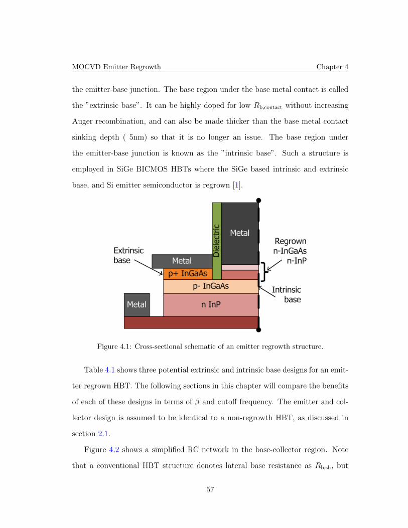
MOCVD Emitter Regrowth Chapter 4
the emitter-base junction. The base region under the base metal contact is called
the ”extrinsic base”. It can be highly doped for low Rb,contact without increasing
Auger recombination, and can also be made thicker than the base metal contact
sinking depth ( 5nm) so that it is no longer an issue. The base region under
the emitter-base junction is known as the ”intrinsic base”. Such a structure is
employed in SiGe BICMOS HBTs where the SiGe based intrinsic and extrinsic
base, and Si emitter semiconductor is regrown [1].
Figure 4.1: Cross-sectional schematic of an emitter regrowth structure.
Table 4.1 shows three potential extrinsic and intrinsic base designs for an emit-
ter regrown HBT. The following sections in this chapter will compare the benefits
of each of these designs in terms of β and cutoff frequency. The emitter and col-
lector design is assumed to be identical to a non-regrowth HBT, as discussed in
section 2.1.
Figure 4.2 shows a simplified RC network in the base-collector region. Note
that a conventional HBT structure denotes lateral base resistance as Rb,sh, but
57
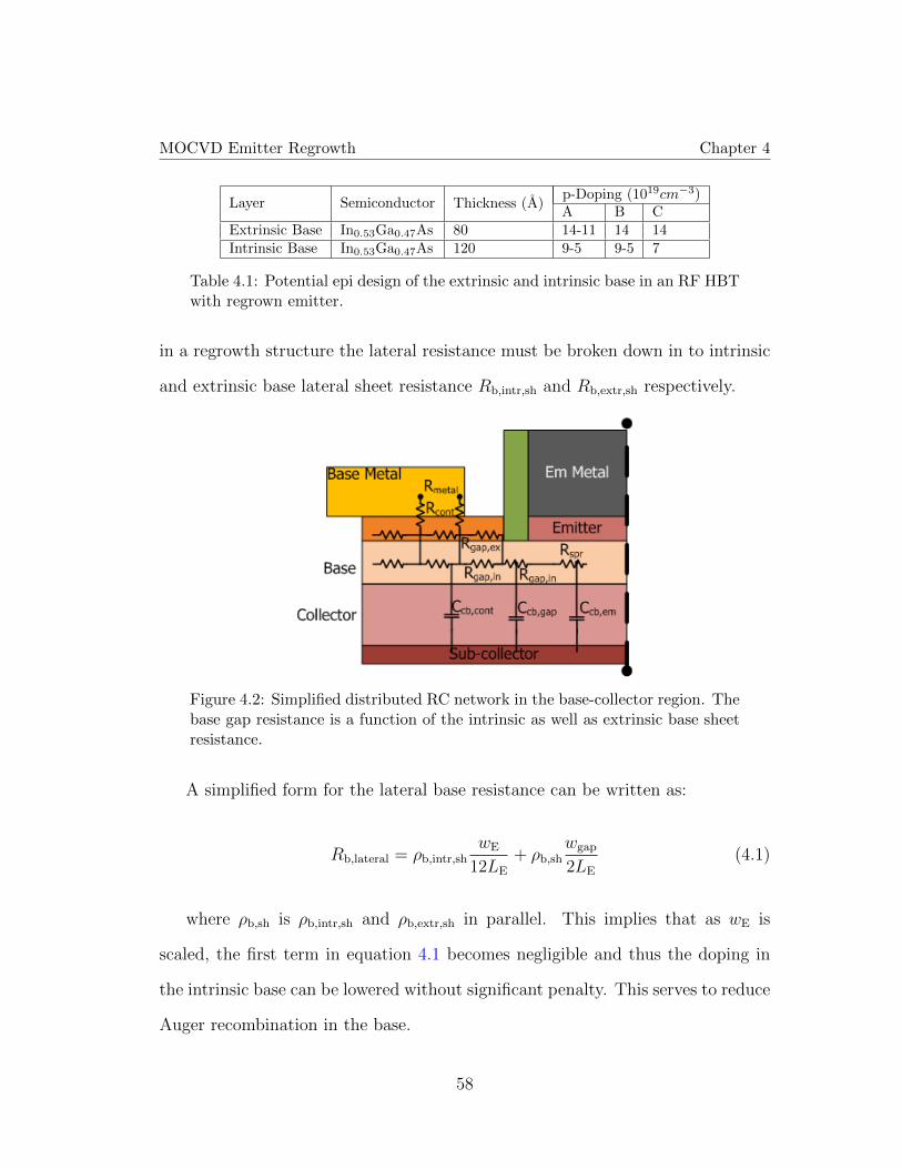
MOCVD Emitter Regrowth Chapter 4
Layer Semiconductor Thickness (A)p-Doping (1019cm−3)A B C
Extrinsic Base In0.53Ga0.47As 80 14-11 14 14Intrinsic Base In0.53Ga0.47As 120 9-5 9-5 7
Table 4.1: Potential epi design of the extrinsic and intrinsic base in an RF HBTwith regrown emitter.
in a regrowth structure the lateral resistance must be broken down in to intrinsic
and extrinsic base lateral sheet resistance Rb,intr,sh and Rb,extr,sh respectively.
Figure 4.2: Simplified distributed RC network in the base-collector region. Thebase gap resistance is a function of the intrinsic as well as extrinsic base sheetresistance.
A simplified form for the lateral base resistance can be written as:
Rb,lateral = ρb,intr,shwE
12LE
+ ρb,shwgap
2LE
(4.1)
where ρb,sh is ρb,intr,sh and ρb,extr,sh in parallel. This implies that as wE is
scaled, the first term in equation 4.1 becomes negligible and thus the doping in
the intrinsic base can be lowered without significant penalty. This serves to reduce
Auger recombination in the base.
58
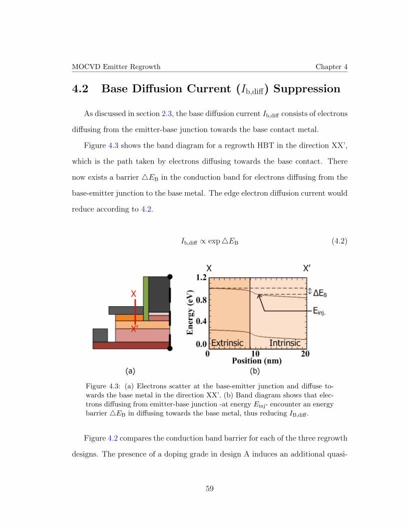
MOCVD Emitter Regrowth Chapter 4
4.2 Base Diffusion Current (Ib,diff) Suppression
As discussed in section 2.3, the base diffusion current Ib,diff consists of electrons
diffusing from the emitter-base junction towards the base contact metal.
Figure 4.3 shows the band diagram for a regrowth HBT in the direction XX’,
which is the path taken by electrons diffusing towards the base contact. There
now exists a barrier 4EB in the conduction band for electrons diffusing from the
base-emitter junction to the base metal. The edge electron diffusion current would
reduce according to 4.2.
Ib,diff ∝ exp4EB (4.2)
Figure 4.3: (a) Electrons scatter at the base-emitter junction and diffuse to-wards the base metal in the direction XX’. (b) Band diagram shows that elec-trons diffusing from emitter-base junction -at energy Einj- encounter an energybarrier 4EB in diffusing towards the base metal, thus reducing IB,diff .
Figure 4.2 compares the conduction band barrier for each of the three regrowth
designs. The presence of a doping grade in design A induces an additional quasi-
59

MOCVD Emitter Regrowth Chapter 4
electric field ~εQuasi that inhibits electron transport to the base contact.
Design Energy Barrier (meV) ~εQuasi
A 53 3.7× 10⁴
B 53 -C 78 -
Table 4.2: Energy barrier and quasi-electric field ~εQuasi that suppress Ib,diff ineach of the proposed regrowth base designs.
4.3 Reduction Of Auger Recombination In The
Base
Auger recombination occurs in the intrinsic base as electrons travel from
the emitter-base junction towards the base-collector. In the regrowth structure,
the intrinsic base doping can be lower than the doping in a conventional HBT
structure, because the base metal contact is now contacting the extrinsic base
instead.
The Auger recombination profile along the intrinsic base can be calculated for
each of the proposed designs, similar to section 3.4.
4.4 Increase in ft
For a regrowth structure, the lateral base sheet resistance needs to be
considered separately under the emitter-base junction and under the extrinsic base
region. As the thickness and doping of the extrinsic base are largely determined
by process considerations, it can be made thicker and with high doping. As shown
60

MOCVD Emitter Regrowth Chapter 4
in 4.1, this allows for the intrinsic base doping and thickness to be reduced and
the unity-gain cut-off frequency ft to be increased.
Table 4.3 shows multiple regrowth epi designs at 100 nm wE and compares
their respective ft, fmax using equations 2.15 and 2.16. The base access resistance
Rbb is computed using 2.8 for conventional HBTs, and modified according to
section 4.1 for regrowth HBTs. All resistance, and capacitance values are taken
from values extracted from RF HBTs fabricated at UCSB [2]. A detailed list of
variables and their values can be found in Appendix A.
Design Rb,spread(Ω) Rb,gap(Ω) Rb,contact(Ω) τb(fs) ft (GHz) fmax (GHz)A 8.6 4.2 24.5 48 577 1379B 7.75 3.9 24.2 48 577 1406C 7.75 3.9 24.2 48 577 1406
HBT64C 4.8 4.3 24.6 80 517 1374
Table 4.3: Base access resistance comparison for the proposed regrowth designs,compared with a non-regrowth device HBT 64C fabricated at UCSB with a20nm base [2]. Emitter width of 100 nm is assumed
The regrowth designs show an improvement in cutoff frequency due to a thin-
ner intrinsic base and lower base transit time (τb). In spite of a thinner intrinsic
base, all base resistance components except for Rb,spread show comparable values
to HBT 64C. However, Rb,spread for regrowth and non-regrowth designs converge
as the emitter width scales further.
4.5 Regrowth as a Viable Technology
The regrowth HBT structure can be grown either by regrowing the extrinsic
base around the emitter [3], or by regrowing the emitter after etching a gap in the
extrinsic base [4]. This section explores the viability of each approach based on
61
MOCVD Emitter Regrowth Chapter 4
capabilities of existing growth technologies.
Base regrowth of the extrinsic base region has three advantages over emitter
regrowth. Firstly, the regrowth interface is not in the active emitter-base depletion
region unlike emitter regrowth. Secondly, the emitter metal can be formed prior
to base regrowth, thus allowing for blanket base regrowth without the need for
any additional lithography steps. Thirdly, the base regrowth width does not scale
as the emitter width is scaled for higher RF performance. The extrinsic regrowth
p-InGaAs must have high doping >1*1020cm−3 and have good crystalline growth
for low Rbb.
Using MBE to regrow highly doped p-InGaAs extrinsic base around dummy
refractory metal emitters have yielded poor morphology growth [5] which leads
to higher Rbb, and is a source of interference when using e-beam lithography for
subsequent steps [6].
MOCVD base regrowth is not a viable option as the UCSB Thomas Swan 2
MOCVD reactor uses Zn as a p-dopant and is unable to grow p-InGaAs with a
doping higher than 2*1019cm−3.
Emitter regrowth of the emitter-base junction allows more freedom in choos-
ing the emitter metal, as the emitter metal is deposited after regrowth and is
not exposed to regrowth conditions. Fine control of the regrown semiconductor
doping profile is required for growth of the various emitter layers, and the growth
morphology must be smooth.
MBE regrowth of the InP emitter and InAs emitter cap has been demonstrated
previously [7]. Though the technology yields RF HBTs at 700nm emitter width,
it is unable to scale to to the 100nm node. The MBE regrowth is non-selective
62
MOCVD Emitter Regrowth Chapter 4
and grows on the sidewalls of the regrowth window, thus limiting the minimum
regrowth window width. The regrowth is poly-crystalline which adds to Rex and
this is exacerbated as emitter width shrinks. Lastly, the process for MBE emitter
regrowth requires that the emitter metal be aligned to the regrowth which adds
significant complexity to the device process flow.
This work proposes selective MOCVD regrowth of the emitter semiconduc-
tor using a self-aligned process flow. It has previously been demonstrated at
UCSB that silicon doped n-type InP/InGaAs regrown via MOCVD has excel-
lent morphology, low contact resistance, and is selective with no growth on oxide
masks [8] [9]. A viable HBT technology that utilizes MOCVD emitter regrowth
must be able to scale ≤ 100nm, maintain low Rex, Rbb, Rcc, and use a self-aligned
emitter metal process.
A major challenge with MOCVD regrowth is that it introduces hydrogen at
high temperatures. The H+ bonds with carbon p dopant in the p-InGaAs and
passivates it. Reactivating the carbon doping in the base post-regrowth is critical
for the process to be successful. It has been shown that the hydrogen can be
removed and the carbon reactivated by annealing samples at 500oC for >10min
under N2 ambient [10]. However, it was discovered that this damages the p-
InGaAs surface. Section 5 discusses the source of this damage, its implications,
and the steps taken to minimize the damage to yield working transistors.
63
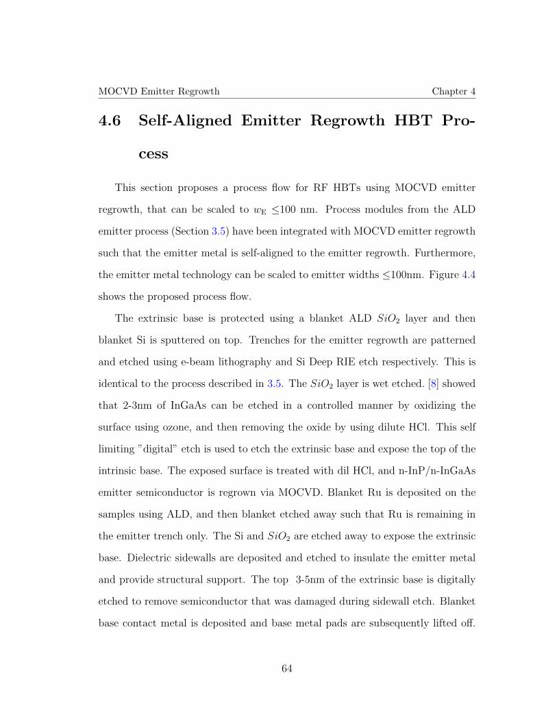
MOCVD Emitter Regrowth Chapter 4
4.6 Self-Aligned Emitter Regrowth HBT Pro-
cess
This section proposes a process flow for RF HBTs using MOCVD emitter
regrowth, that can be scaled to wE ≤100 nm. Process modules from the ALD
emitter process (Section 3.5) have been integrated with MOCVD emitter regrowth
such that the emitter metal is self-aligned to the emitter regrowth. Furthermore,
the emitter metal technology can be scaled to emitter widths ≤100nm. Figure 4.4
shows the proposed process flow.
The extrinsic base is protected using a blanket ALD SiO2 layer and then
blanket Si is sputtered on top. Trenches for the emitter regrowth are patterned
and etched using e-beam lithography and Si Deep RIE etch respectively. This is
identical to the process described in 3.5. The SiO2 layer is wet etched. [8] showed
that 2-3nm of InGaAs can be etched in a controlled manner by oxidizing the
surface using ozone, and then removing the oxide by using dilute HCl. This self
limiting ”digital” etch is used to etch the extrinsic base and expose the top of the
intrinsic base. The exposed surface is treated with dil HCl, and n-InP/n-InGaAs
emitter semiconductor is regrown via MOCVD. Blanket Ru is deposited on the
samples using ALD, and then blanket etched away such that Ru is remaining in
the emitter trench only. The Si and SiO2 are etched away to expose the extrinsic
base. Dielectric sidewalls are deposited and etched to insulate the emitter metal
and provide structural support. The top 3-5nm of the extrinsic base is digitally
etched to remove semiconductor that was damaged during sidewall etch. Blanket
base contact metal is deposited and base metal pads are subsequently lifted off.
64
MOCVD Emitter Regrowth Chapter 4
Figure 4.4: Process flow for fabricating emitter regrowth HBTs with a self--aligned emitter metal deposited via ALD. HBT fabrication steps after (g) areidentical to W/TiW emitter HBT process flow shown in Appendix B.
65

MOCVD Emitter Regrowth Chapter 4
The active device region is protected and the base-collector wet-etched down to
the sub-collector InGaAs cap. Collector contacts are lifted off and the device is
isolated. A PECVD SiN layer is deposited for structural support and the device
is planarized via BCB. A low temperature SiN layer is deposited as an anchor
(Section 3.1) and the first metal layer is lifted off.
Since the emitter metal is deposited in the trench that was etched as a regrowth
window, it is not required to align the emitter metal to the regrowth. This is
important as an aligned process increases the process complexity, especially as the
emitter width is scaled. Note that the step to anneal the sample and reactivate
carbon doping is not mentioned here, as it is discussed in detail in chapter 5.
66
REFERENCES
References
[1] Pekarik, J.J.; Adkisson, J.; Gray, P.; Liu, Q.; Camillo-Castillo, R.; Khater,M.; Jain, V.; Zetterlund, B.; DiVergilio, A.; Tian, X.; Vallett, A.; Ellis-Monaghan, J.; Gross, B.J.; Cheng, P.; Kaushal, V.; He, Z.; Lukaitis, J.;Newton, K.; Kerbaugh, M.; Cahoon, N.; Vera, L.; Zhao, Y.; Long, J.R.;Valdes-Garcia, A.; Reynolds, S.; Lee, W.; Sadhu, B.; Harame, D., ”A 90nmSiGe BiCMOS technology for mm-wave and high-performance analog appli-cations,” in Bipolar/BiCMOS Circuits and Technology Meeting (BCTM),2014 IEEE , vol., no., pp.92-95, Sept. 28 2014-Oct. 1 2014
[2] J. Rode, IC Fabrication Technology for Highly Scaled THz DHBTs.. Ph.D.Thesis, University of California, Santa Barbara, Santa. Barbara, Ca, U.S.A.,2015.
[3] Shimawaki, H.; Amamiya, Y.; Furuhata, Naoki; Honjo, K., ”High-fmax Al-GaAs/InGaAs and AlGaAs/GaAs HBT’s with p+/p regrown base contacts,”in Electron Devices, IEEE Transactions on , vol.42, no.10, pp.1735-1744, Oct1995
[4] Fu, S.L.; Park, S.; Hsin, Y.M.; Ho, M.C.; Chin, T.P.; Yu, P.L.; Tu, C.W.;Asbeck, P.M., ”GaInP/GaAs HBTs with selectively regrown emitter and widebandgap extrinsic base,” in Device Research Conference, 1994. 52nd Annual, vol., no., pp.91-92, 1994
[5] A. Baraskar, (Development of Ultra-Low Resistance Ohmic Contacts forInGaAs/InP HBTs.. PhD thesis. University of California, Santa Barbara,Santa. Barbara, Ca, U.S.A., 2011.
[6] Nonalloyed and alloyed lowresistance ohmic contacts with good morphologyfor GaAs using a graded InGaAs cap layer. Mehdi, I. and Reddy, U. K. andOh, J. and East, J. R. and Haddad, G. I., Journal of Applied Physics, 65,867-869 (1989)
[7] D. Scott, (Indium Phosphide Heterojunction Bipolar Transistors with Emit-ter Regrowth by Molecular Beam Epitaxy.. PhD thesis.
[8] S. Lee, C. Y. Huang, A. D. Carter, D. C. Elias, J. J. M. Law, V. Chobpattana,S. Krmer, B. J. Thibeault, W. Mitchell, S. Stemmer, A. C. Gossard, and. M.J. W. Rodwell, Record Extrinsic Transconductance (2.45 mS/m at VDS. =0.5 V) InAs/In0.53GaAs Channel MOSFETs Using MOCVD Source-Drain.Regrowth, Symposium on VLSI Technology, T246, 2013.
67

REFERENCES
[9] C-Y. Huang, (III-V Ultra-Thin-Body InGaAs/InAs MOSFETs for LowStandby Power Logic Applications.. PhD thesis.
[10] Noriyuki Watanabe, Shoji Yamahata, Takashi Kobayashi, Hydrogen removalby annealing from C-doped InGaAs grown on InP by metalorganic chemicalvapor deposition, Journal of Crystal Growth, Volume 200, Issues 34, April1999, Pages 599-602, ISSN 0022-0248
68

Chapter 5
Experimental Results and
Analysis
This chapter lists the challenges faced in reactivating carbon doping in the p-
InGaAs base, the fabrication processes explored to minimize base surface damage
and base contact resistivity, and the I-V characteristics of HBTs fabricated using
MOCVD selective emitter regrowth. The HBTs fabricated were Large Area De-
vices (LAD) as this allows for rapid prototyping and troubleshooting. The process
flow for LADs is also listed.
5.1 Carbon Passivation of p-InGaAs Base
[1] has shown that hydrogen can be removed and carbon doping reactivated in
p-InGaAs by annealing in N2 ambient at 500oC for 10 min. The hole concentration
in the p-InGaAs layers was measured using Hall measurement [2]. The experiment
69

Experimental Results and Analysis Chapter 5
was repeated at UCSB, using an AET RX6 Rapid Thermal Processor to anneal
in a N2 ambient at 500oC for 10 min. Figure 5.1 summarizes the results of the
annealing study. A 10 nm ALD SiO2 cap was used to prevent As out-diffusion
and chamber contamination.
Hall p-Conc.(1019cm−3)Film Anneal (nm)
Process Thickness(nm) Chamber/Gas Before After AfterProcess Regrowth Anneal
Regrow n-InP 20 RTA/N2 10 0.7 5.5Wet etch InP 200 RTA/N2 10 0.7 9
No 20 RTA/N2 10 - 5.5process 20 MBE/As 10 - 9.5
Table 5.1: Hall hole carrier concentration of p-InGaAs films after various pro-cessing and anneal conditions.
It was observed that the hole carrier concentration measured after annealing
was a function of the film thickness. ≈55% of the hole concentration was reacti-
vated on a 20nm InGaAs film, vs 90% for a 200nm thick film. This suggests that
the p-InGaAs surface is damaged. A high carrier concentration is observed for
samples that were annealed in an MBE chamber under As over-pressure. Thus,
the surface damage in samples is due to As out-diffusion through the SiO2 cap. It
is unclear if this is during regrowth or anneal. Section 5.4 discusses this in further
detail to show that the bulk of surface damage is during the annealing step with
an oxide anneal cap.
70

Experimental Results and Analysis Chapter 5
5.2 Large Area Device HBT Emitter Regrowth
Process
Modern HBTs employ base thicknesses of 15-30 nm with a base doping of
9-10*1019cm−3 at the emitter-base junction. The regrowth process and anneal
shown in 5.1 would lead to a doping of 4.95-5.5*1019cm−3 at the base surface
after regrowth and anneal. While the doping is not ideal, it is sufficiently high for
forming ohmic base contacts [3].
LADs were fabricated using the aforementioned annealing process with an ox-
ide cap, in order to extract the regrown emitter access resistance, and emitter-base
diode characteristics. A LAD structure was used as it reduces process complexity
and thus allows for rapid prototyping and troubleshooting. Figure 5.1 shows the
process flow used for LADs.
Note that this process is different from the self-aligned emitter process in
section 4.6. The primary difference being that the regrowth window mask is
purely SiO2 rather than SiO2/Si, and that the lifted-off emitter metal is aligned
to the regrowth window. The emitter width for LADs ranges from 500-4000 nm.
In this process, an ALD SiO2 cap is deposited as an annealing cap after the
regrowth mask is wet-etched away. The sample is annealed to reactivate the
carbon doping, and base contacts are lifted off after removing the annealing cap.
The remainder of the process is identical to the the self-aligned emitter process.
71

Experimental Results and Analysis Chapter 5
Figure 5.1: Process flow for a Large Area Device (LAD) HBT with emitterregrowth. Steps after (i) are identical to RF HBT process in Appendix B.
72

Experimental Results and Analysis Chapter 5
5.3 HBT 68Q4 - Oxide Protective Cap
5.3.1 Device Structure and Process Feature
HBT68 utilizes a 15nm extrinsic InGaAs base that is doped 9-6.6*1019cm−3,
and a 10nm intrinsic base doped from 6.6-5*1019cm−3 from emitter to collector.
The design employs a 100nm collector structure (setback, superlattice, InP collec-
tor) with doping concentration of 5*1016cm−3. The detailed epitaxial structure is
listed in table 5.2. The emitter structure listed is regrown using MOCVD. Note
that the extrinsic base is highlighted in yellow and is not below the emitter-base
junction, but to the side. It should be noted that HBT 68 was designed for RF
Layer Semiconductor Thickness (A) Doping (cm−3)Emitter cap In0.53Ga0.47As 100 8× 10¹⁹:Si
Emitter InP 50 5× 10¹⁹:SiEmitter InP 150 3× 10¹⁸:Si
Extrinsic Base In0.53Ga0.47As 150 9− 6.6× 10¹⁹:C
Intrinsic Base In0.53Ga0.47As 100 6.6− 5× 10¹⁹:CSetback In0.53Ga0.47As 135 5× 10¹⁶:Si
B-C grade - 165 5× 10¹⁶:Siδ-doping InP 30 3.6× 10¹⁸:SiCollector InP 670 5× 10¹⁶:Si
Sub-collector InP 75 2× 10¹⁹:SiSub-collector In0.53Ga0.47As 75 4× 10¹⁹:SiSub-collector InP 3000 1× 10¹⁹:Si
Etch stop In0.53Ga0.47As 35 undopedSubstrate InP - undoped
Table 5.2: Epitaxial structure of HBT 68. The emitter-base junction is formedat the Emitter-Intrinsic base interface, and the extrinsic base lies on either sideof this junction, on top of the intrinsic base.
HBTs at the 100nm emitter width node, and thus there is no clear doping step
between the intrinsic and extrinsic base.
73
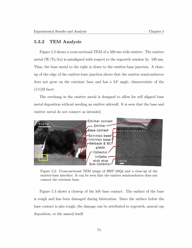
Experimental Results and Analysis Chapter 5
5.3.2 TEM Analysis
Figure 5.2 shows a cross sectional TEM of a 500 nm wide emitter. The emitter
metal (W/Ti/Au) is misaligned with respect to the regrowth window by 100 nm.
Thus, the base metal to the right is closer to the emitter-base junction. A close-
up of the edge of the emitter-base junction shows that the emitter semiconductor
does not grow on the extrinsic base and has a 54o angle, characteristic of the
(111)B facet.
The overhang in the emitter metal is designed to allow for self aligned base
metal deposition without needing an emitter sidewall. It is seen that the base and
emitter metal do not connect as intended.
Figure 5.2: Cross-sectional TEM image of HBT 68Q4 and a close-up of theemitter-base interface. It can be seen that the emitter semiconductor does notcontact the extrinsic base.
Figure 5.3 shows a closeup of the left base contact. The surface of the base
is rough and has been damaged during fabrication. Since the surface below the
base contact is also rough, the damage can be attributed to regrowth, anneal cap
deposition, or the anneal itself.
74

Experimental Results and Analysis Chapter 5
Figure 5.3: Cross-sectional TEM of the base surface and base contact of HBT68Q4. The base surface is damaged.
5.3.3 DC Characteristics
TLM measurement structures were included in the mask design for measuring
emitter, base, and collector contact resistivity. The emitter TLM test structures
could not be measured as the semiconductor in the TLM gap spacing was etched
during isolation due to poor photoresist adhesion. Base TLM structures indicate
contact resistivity of 3500 Ω.µm2. Failure to remove the oxide annealing cap prior
to metal deposition is ruled out by the TEM images. The extracted base sheet
resistance was measured to be 2470 Ω/2, up from a sheet resistance of 1248 Ω/2
measured before regrowth via four-point measurement. Thus, only 50% of the
carbon dopants were reactivated during the anneal. A base doping of 4*1019cm−3
yields contact resistivity <100 Ω.µm2 [4], thus the base contacts resistivity should
be much lower than measured. Collector contact resistivity was measured to be
34 Ω.µm2.
Figure 5.4-5.5 show the emitter-base diode, base collector diode, and forward-
active gummel characteristics of a transistor of emitter area 0.4x8µm2. The base-
collector area is 4.2x11 µm2.
75
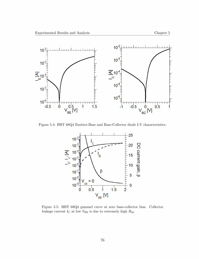
Experimental Results and Analysis Chapter 5
Figure 5.4: HBT 68Q4 Emitter-Base and Base-Collector diode I-V characteristics.
Figure 5.5: HBT 68Q4 gummel curve at zero base-collector bias. Collectorleakage current IC at low VBE is due to extremely high Rbb
76
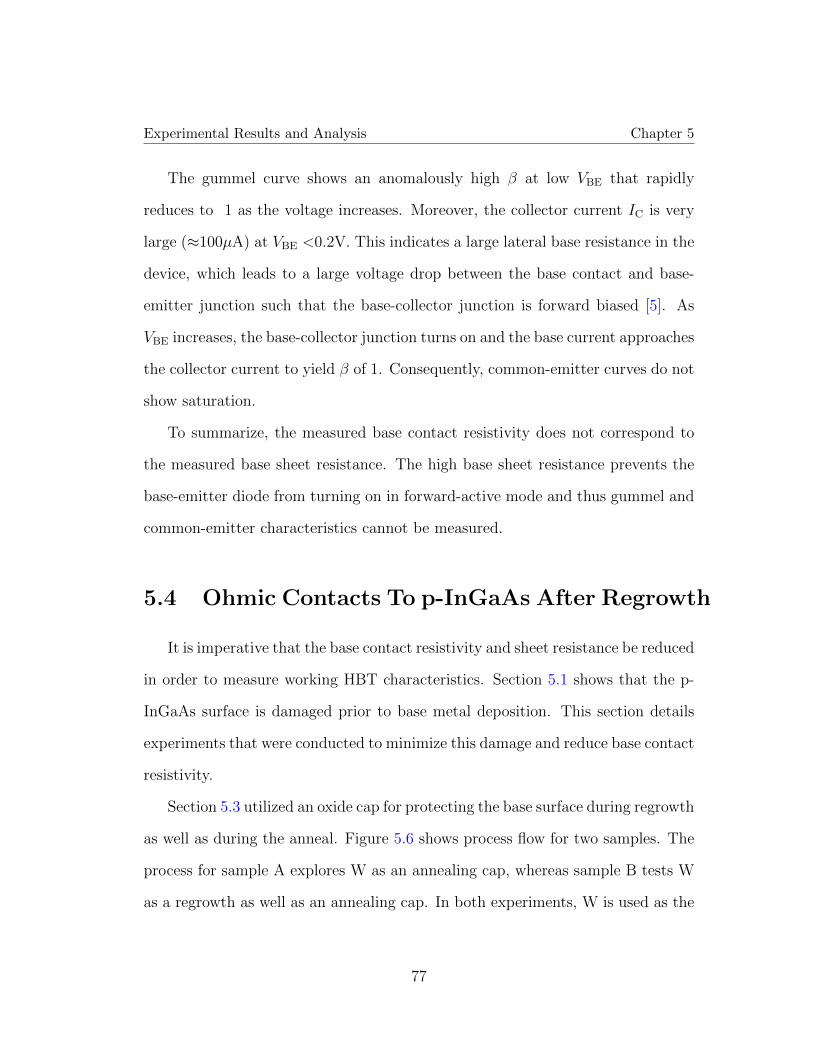
Experimental Results and Analysis Chapter 5
The gummel curve shows an anomalously high β at low VBE that rapidly
reduces to 1 as the voltage increases. Moreover, the collector current IC is very
large (≈100µA) at VBE <0.2V. This indicates a large lateral base resistance in the
device, which leads to a large voltage drop between the base contact and base-
emitter junction such that the base-collector junction is forward biased [5]. As
VBE increases, the base-collector junction turns on and the base current approaches
the collector current to yield β of 1. Consequently, common-emitter curves do not
show saturation.
To summarize, the measured base contact resistivity does not correspond to
the measured base sheet resistance. The high base sheet resistance prevents the
base-emitter diode from turning on in forward-active mode and thus gummel and
common-emitter characteristics cannot be measured.
5.4 Ohmic Contacts To p-InGaAs After Regrowth
It is imperative that the base contact resistivity and sheet resistance be reduced
in order to measure working HBT characteristics. Section 5.1 shows that the p-
InGaAs surface is damaged prior to base metal deposition. This section details
experiments that were conducted to minimize this damage and reduce base contact
resistivity.
Section 5.3 utilized an oxide cap for protecting the base surface during regrowth
as well as during the anneal. Figure 5.6 shows process flow for two samples. The
process for sample A explores W as an annealing cap, whereas sample B tests W
as a regrowth as well as an annealing cap. In both experiments, W is used as the
77
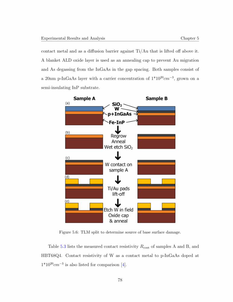
Experimental Results and Analysis Chapter 5
contact metal and as a diffusion barrier against Ti/Au that is lifted off above it.
A blanket ALD oxide layer is used as an annealing cap to prevent Au migration
and As degassing from the InGaAs in the gap spacing. Both samples consist of
a 20nm p-InGaAs layer with a carrier concentration of 1*1020cm−3, grown on a
semi-insulating InP substrate.
Figure 5.6: TLM split to determine source of base surface damage.
Table 5.3 lists the measured contact resistivity Rcont of samples A and B, and
HBT68Q4. Contact resistivity of W as a contact metal to p-InGaAs doped at
1*1020cm−3 is also listed for comparison [4].
78
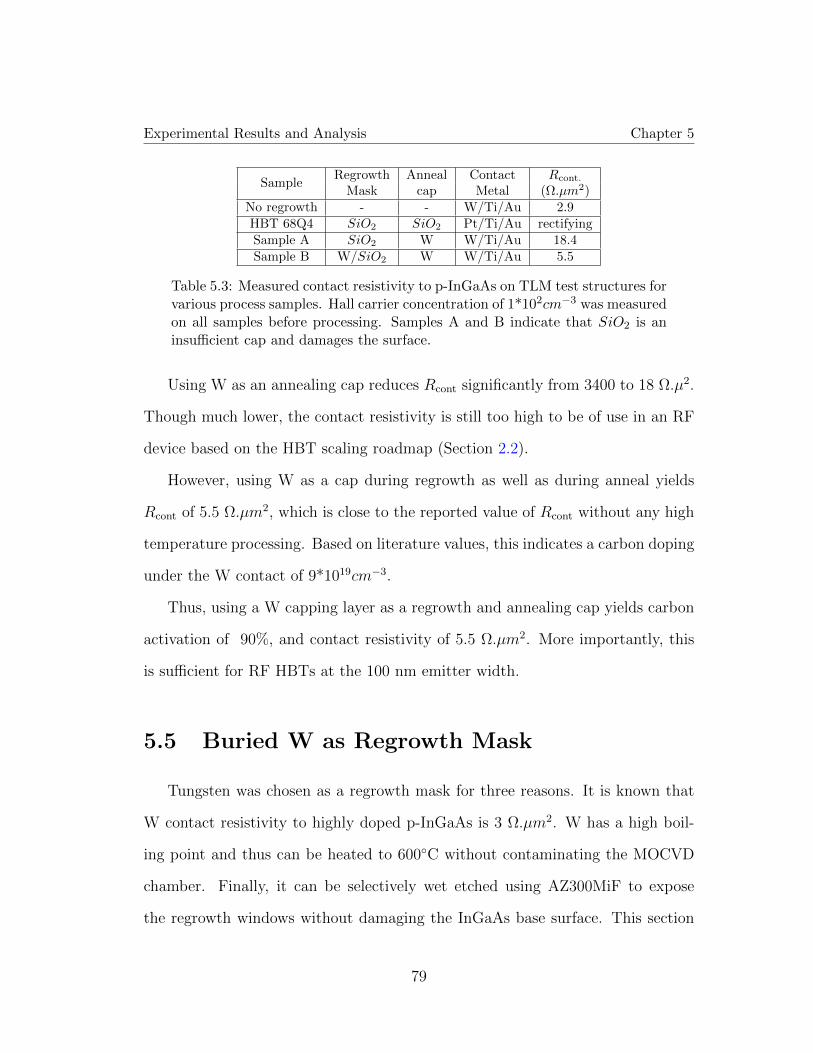
Experimental Results and Analysis Chapter 5
SampleRegrowth Anneal Contact Rcont.
Mask cap Metal (Ω.µm2)No regrowth - - W/Ti/Au 2.9HBT 68Q4 SiO2 SiO2 Pt/Ti/Au rectifyingSample A SiO2 W W/Ti/Au 18.4Sample B W/SiO2 W W/Ti/Au 5.5
Table 5.3: Measured contact resistivity to p-InGaAs on TLM test structures forvarious process samples. Hall carrier concentration of 1*102cm−3 was measuredon all samples before processing. Samples A and B indicate that SiO2 is aninsufficient cap and damages the surface.
Using W as an annealing cap reduces Rcont significantly from 3400 to 18 Ω.µ2.
Though much lower, the contact resistivity is still too high to be of use in an RF
device based on the HBT scaling roadmap (Section 2.2).
However, using W as a cap during regrowth as well as during anneal yields
Rcont of 5.5 Ω.µm2, which is close to the reported value of Rcont without any high
temperature processing. Based on literature values, this indicates a carbon doping
under the W contact of 9*1019cm−3.
Thus, using a W capping layer as a regrowth and annealing cap yields carbon
activation of 90%, and contact resistivity of 5.5 Ω.µm2. More importantly, this
is sufficient for RF HBTs at the 100 nm emitter width.
5.5 Buried W as Regrowth Mask
Tungsten was chosen as a regrowth mask for three reasons. It is known that
W contact resistivity to highly doped p-InGaAs is 3 Ω.µm2. W has a high boil-
ing point and thus can be heated to 600C without contaminating the MOCVD
chamber. Finally, it can be selectively wet etched using AZ300MiF to expose
the regrowth windows without damaging the InGaAs base surface. This section
79

Experimental Results and Analysis Chapter 5
demonstrates a process flow where W base contacts are deposited on the extrinsic
base, and the emitter regrowth windows are etched in afterwards.
Figure 5.7 shows cross-sectional SEM images of where regrowth windows have
been etched into a blanket W/SiO2 stack. The W undercut after being etched in
AZ300MiF suggests that W was successfully wet etched in the regrowth windows.
The fabrication process after regrowth remains the same as before, except that
the blanket W base contact is already there.
Figure 5.7: Cross-sectional SEM of a regrowth window after the buried W hasbeen wet-etched using AZ300MiF. The undercut is visible at the trench corner.The extrinsic base is then digitally etched and the emitter is regrown.
Emitter semiconductor was regrown on HBT epi using the above process.
Figure 5.8 shows a cross-sectional SEM of a sample post regrowth. There is
nucleation in select areas in the growth window, but most of the regrowth window
shows no growth. This suggests presence of a residual layer on the p-InGaAs that
is inhibiting growth. Furthermore, the p-InGaAs at the lateral W boundary has
been etched away.
An additional CF4/O2 descum was performed prior to regrowth, as a means of
80
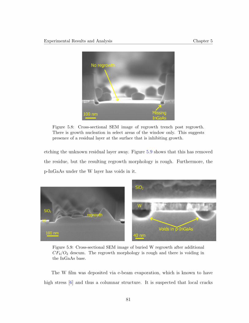
Experimental Results and Analysis Chapter 5
Figure 5.8: Cross-sectional SEM image of regrowth trench post regrowth.There is growth nucleation in select areas of the window only. This suggestspresence of a residual layer at the surface that is inhibiting growth.
etching the unknown residual layer away. Figure 5.9 shows that this has removed
the residue, but the resulting regrowth morphology is rough. Furthermore, the
p-InGaAs under the W layer has voids in it.
Figure 5.9: Cross-sectional SEM image of buried W regrowth after additionalCF4/O2 descum. The regrowth morphology is rough and there is voiding inthe InGaAs base.
The W film was deposited via e-beam evaporation, which is known to have
high stress [6] and thus a columnar structure. It is suspected that local cracks
81
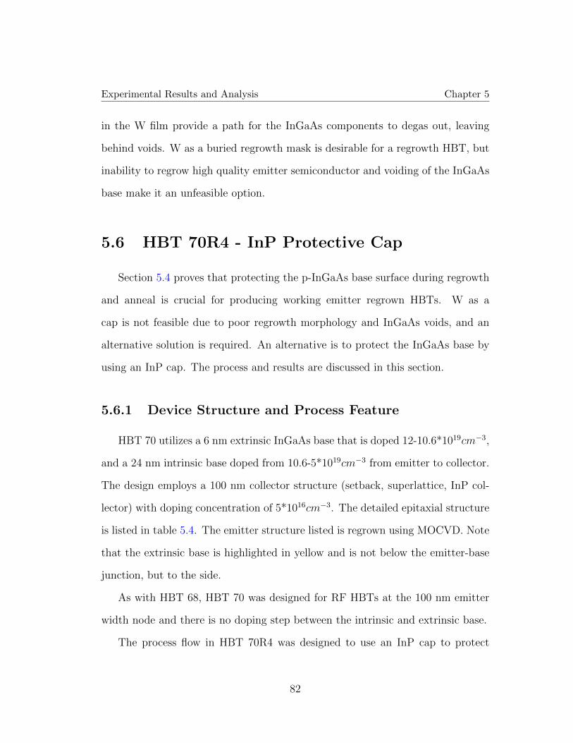
Experimental Results and Analysis Chapter 5
in the W film provide a path for the InGaAs components to degas out, leaving
behind voids. W as a buried regrowth mask is desirable for a regrowth HBT, but
inability to regrow high quality emitter semiconductor and voiding of the InGaAs
base make it an unfeasible option.
5.6 HBT 70R4 - InP Protective Cap
Section 5.4 proves that protecting the p-InGaAs base surface during regrowth
and anneal is crucial for producing working emitter regrown HBTs. W as a
cap is not feasible due to poor regrowth morphology and InGaAs voids, and an
alternative solution is required. An alternative is to protect the InGaAs base by
using an InP cap. The process and results are discussed in this section.
5.6.1 Device Structure and Process Feature
HBT 70 utilizes a 6 nm extrinsic InGaAs base that is doped 12-10.6*1019cm−3,
and a 24 nm intrinsic base doped from 10.6-5*1019cm−3 from emitter to collector.
The design employs a 100 nm collector structure (setback, superlattice, InP col-
lector) with doping concentration of 5*1016cm−3. The detailed epitaxial structure
is listed in table 5.4. The emitter structure listed is regrown using MOCVD. Note
that the extrinsic base is highlighted in yellow and is not below the emitter-base
junction, but to the side.
As with HBT 68, HBT 70 was designed for RF HBTs at the 100 nm emitter
width node and there is no doping step between the intrinsic and extrinsic base.
The process flow in HBT 70R4 was designed to use an InP cap to protect
82

Experimental Results and Analysis Chapter 5
Layer Semiconductor Thickness (A) Doping (cm−3)Emitter cap In0.53Ga0.47As 100 8× 10¹⁹:Si
Emitter InP 50 5× 10¹⁹:SiEmitter InP 150 3× 10¹⁸:Si
Extrinsic Base In0.53Ga0.47As 60 12− 10.6× 10¹⁹:C
Intrinsic Base In0.53Ga0.47As 240 10.6− 5× 10¹⁹:CSetback In0.53Ga0.47As 135 5× 10¹⁶:Si
B-C grade - 165 5× 10¹⁶:Siδ-doping InP 30 3.6× 10¹⁸:SiCollector InP 670 5× 10¹⁶:Si
Sub-collector InP 75 2× 10¹⁹:SiSub-collector In0.53Ga0.47As 75 4× 10¹⁹:SiSub-collector InP 3000 1× 10¹⁹:Si
Etch stop In0.53Ga0.47As 35 undopedSubstrate InP - undoped
Table 5.4: Epitaxial structure of HBT 70. The emitter-base junction is formedat the Emitter-Intrinsic base interface, and the extrinsic base lies on either sideof this junction, on top of the intrinsic base.
p-InGaAs during regrowth. Figure 5.10 shows the process flow.
Figure 5.10: Process flow for emitter regrowth HBT LAD that incorporatesan InP cap above the base for minimizing surface damage before base contactmetal deposition. The process after (d) is identical to Figure 5.1, except thatthe W/Ti/Au base metal is deposited prior to ALD oxide and anneal.
The original epitaxial design of HBT 70 includes a InGaAs emitter cap and
83
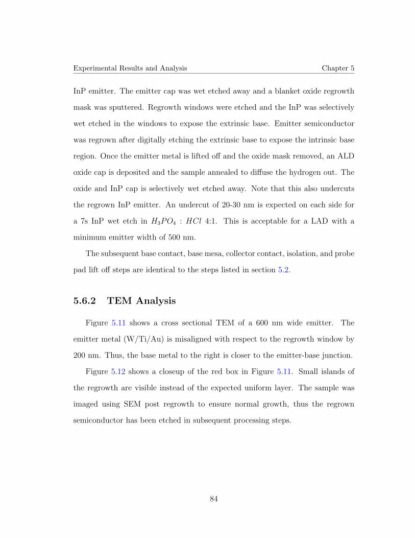
Experimental Results and Analysis Chapter 5
InP emitter. The emitter cap was wet etched away and a blanket oxide regrowth
mask was sputtered. Regrowth windows were etched and the InP was selectively
wet etched in the windows to expose the extrinsic base. Emitter semiconductor
was regrown after digitally etching the extrinsic base to expose the intrinsic base
region. Once the emitter metal is lifted off and the oxide mask removed, an ALD
oxide cap is deposited and the sample annealed to diffuse the hydrogen out. The
oxide and InP cap is selectively wet etched away. Note that this also undercuts
the regrown InP emitter. An undercut of 20-30 nm is expected on each side for
a 7s InP wet etch in H3PO4 : HCl 4:1. This is acceptable for a LAD with a
minimum emitter width of 500 nm.
The subsequent base contact, base mesa, collector contact, isolation, and probe
pad lift off steps are identical to the steps listed in section 5.2.
5.6.2 TEM Analysis
Figure 5.11 shows a cross sectional TEM of a 600 nm wide emitter. The
emitter metal (W/Ti/Au) is misaligned with respect to the regrowth window by
200 nm. Thus, the base metal to the right is closer to the emitter-base junction.
Figure 5.12 shows a closeup of the red box in Figure 5.11. Small islands of
the regrowth are visible instead of the expected uniform layer. The sample was
imaged using SEM post regrowth to ensure normal growth, thus the regrown
semiconductor has been etched in subsequent processing steps.
84
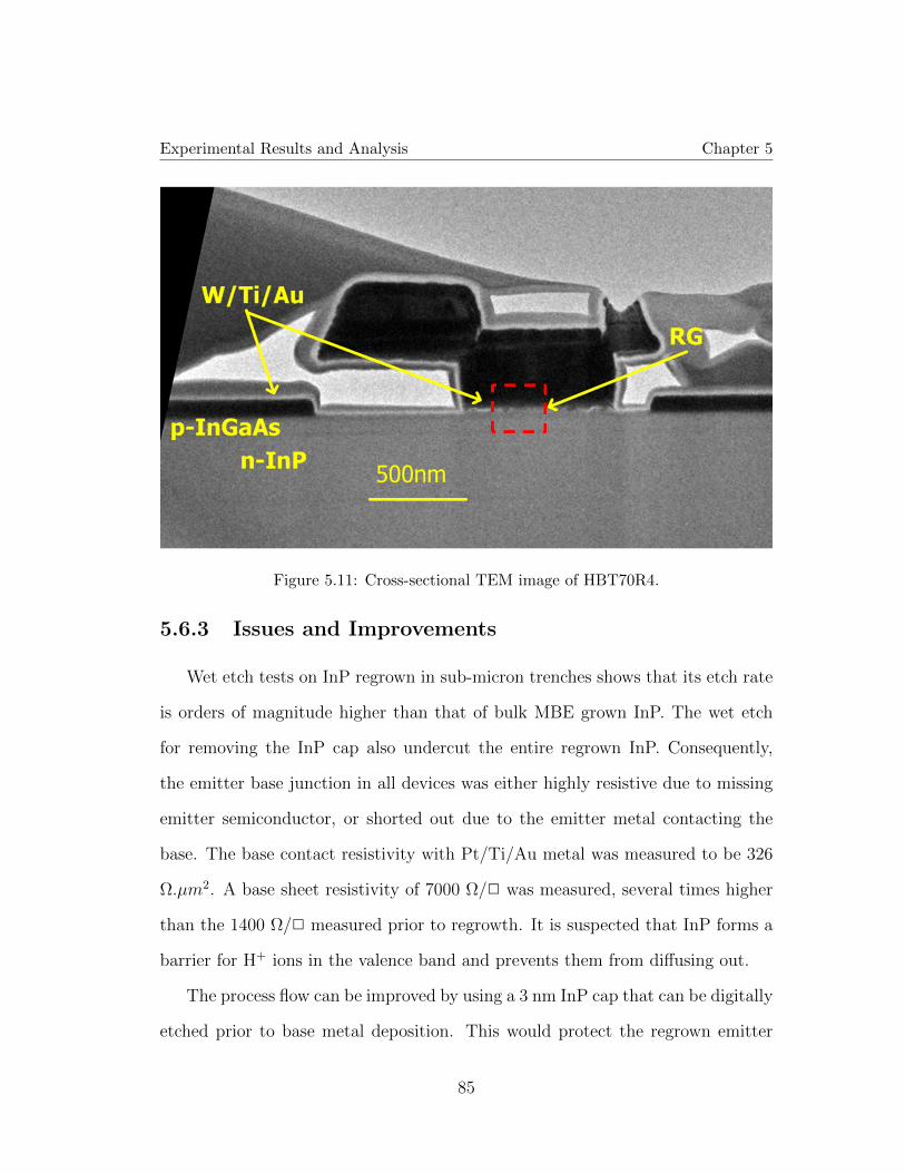
Experimental Results and Analysis Chapter 5
Figure 5.11: Cross-sectional TEM image of HBT70R4.
5.6.3 Issues and Improvements
Wet etch tests on InP regrown in sub-micron trenches shows that its etch rate
is orders of magnitude higher than that of bulk MBE grown InP. The wet etch
for removing the InP cap also undercut the entire regrown InP. Consequently,
the emitter base junction in all devices was either highly resistive due to missing
emitter semiconductor, or shorted out due to the emitter metal contacting the
base. The base contact resistivity with Pt/Ti/Au metal was measured to be 326
Ω.µm2. A base sheet resistivity of 7000 Ω/2 was measured, several times higher
than the 1400 Ω/2 measured prior to regrowth. It is suspected that InP forms a
barrier for H+ ions in the valence band and prevents them from diffusing out.
The process flow can be improved by using a 3 nm InP cap that can be digitally
etched prior to base metal deposition. This would protect the regrown emitter
85

Experimental Results and Analysis Chapter 5
Figure 5.12: Cross-sectional TEM image of the emitter regrowth in HBT70R4.The emitter semiconductor has been etched away during the InP cap wet etch.
semiconductor. A W/Ti/Au base metal can be used and the anneal performed
after base metallization. This would remove the InP barrier and allow H+ ions to
diffuse out.
Unfortunately, an epitaxial design with 3 nm InP cap above the extrinsic base
was unavailable at the time of this experiment and thus could not be explored.
An alternate process for protecting the base surface during anneal is shown in the
following section.
86

Experimental Results and Analysis Chapter 5
5.7 HBT 74 Q4 - W Annealing Cap
Since using a thinner InP regrowth cap and a W annealing cap was not an
option due to epi unavailability. An oxide regrowth cap and W annealing cap
was explored as a way of reducing base contact resistivity, sheet resistance, and
measuring working HBTs with regrown emitter semiconductor. An additional
sample (HBT 74Q1) was fabricated simultaneously using the original epi structure
i.e. no emitter regrowth or anneal was performed on this sample. This section
discusses the process flow and results. DC characteristics of 74Q4 and 74Q1 are
presented as a means of comparing a regrown-emitter with a traditional non-
regrowth device.
5.7.1 Device Structure and Process Feature
HBT70 utilizes a 4nm extrinsic InGaAs base that is doped 12-11*1019cm−3,
and a 16nm intrinsic base doped from 11-7*1019cm−3 from emitter to collector.
The design employs a 70nm collector structure (setback, superlattice, InP collec-
tor) with doping concentration of 1*1017cm−3. The detailed epitaxial structure is
listed in table 5.5. The emitter structure listed is regrown using MOCVD. Note
that the extrinsic base is highlighted in yellow and is not below the emitter-base
junction, but to the side.
As before, HBT74 was designed for RF HBTs at the 100nm emitter width
node and there is no doping step between the intrinsic and extrinsic base.
The process flow in HBT74Q4 was designed to use an oxide cap to protect p-
InGaAs during regrowth and a W cap during anneal similar to Sample in Figure
87

Experimental Results and Analysis Chapter 5
Layer Semiconductor Thickness (A) Doping (cm−3)Emitter cap In0.53Ga0.47As 100 8× 10¹⁹:Si
Emitter InP 150 5× 10¹⁹:SiEmitter InP 150 3× 10¹⁸:Si
Extrinsic Base In0.53Ga0.47As 40 12− 11× 1019:C
Intrinsic Base In0.53Ga0.47As 160 11− 7× 10¹⁹:CSetback In0.53Ga0.47As 50 1× 10¹⁷:Si
B-C grade - 120 1× 10¹⁷:Siδ-doping InP 30 6× 10¹⁸:SiCollector InP 500 1× 10¹⁷:Si
Sub-collector InP 75 2× 10¹⁹:SiSub-collector In0.53Ga0.47As 75 4× 10¹⁹:SiSub-collector InP 3000 1× 10¹⁹:Si
Etch stop In0.53Ga0.47As 35 undopedSubstrate InP - undoped
Table 5.5: Epitaxial structure of HBT74. The emitter-base junction is formedat the Emitter-Intrinsic base interface, and the extrinsic base lies on either sideof this junction, on top of the intrinsic base.
5.6.
The original epitaxial design of HBT74 includes an InGaAs emitter cap and
InP emitter. The emitter was wet etched away and a blanket oxide regrowth mask
was sputtered. Regrowth windows were etched, extrinsic base digitally etched and
the emitter semiconductor was regrown. A blanket W base contact was deposited
after removing the oxide regrowth mask. Ti/Au base metal was lifted off, ALD
oxide cap deposited and the sample was annealed to reactivate the p-InGaAs
carbon doping.
The subsequent base mesa, collector contact, isolation, and probe pad lift off
steps are identical to the steps listed in section 5.2.
88
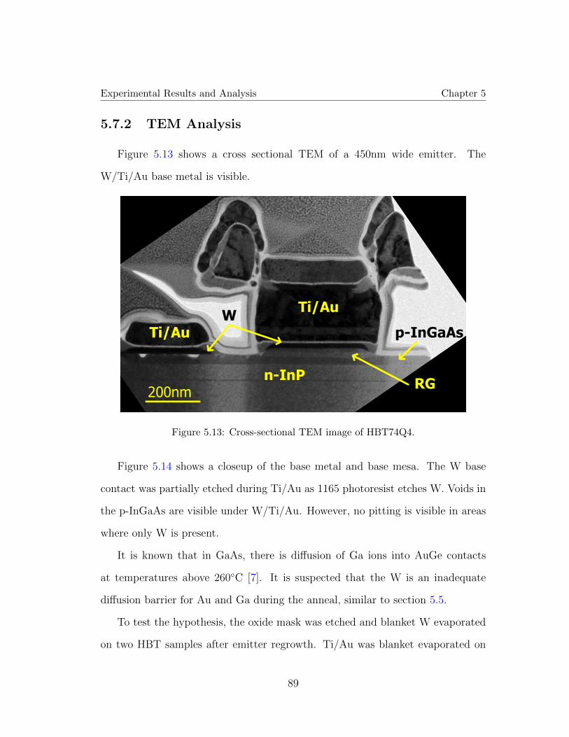
Experimental Results and Analysis Chapter 5
5.7.2 TEM Analysis
Figure 5.13 shows a cross sectional TEM of a 450nm wide emitter. The
W/Ti/Au base metal is visible.
Figure 5.13: Cross-sectional TEM image of HBT74Q4.
Figure 5.14 shows a closeup of the base metal and base mesa. The W base
contact was partially etched during Ti/Au as 1165 photoresist etches W. Voids in
the p-InGaAs are visible under W/Ti/Au. However, no pitting is visible in areas
where only W is present.
It is known that in GaAs, there is diffusion of Ga ions into AuGe contacts
at temperatures above 260C [7]. It is suspected that the W is an inadequate
diffusion barrier for Au and Ga during the anneal, similar to section 5.5.
To test the hypothesis, the oxide mask was etched and blanket W evaporated
on two HBT samples after emitter regrowth. Ti/Au was blanket evaporated on
89

Experimental Results and Analysis Chapter 5
Figure 5.14: Cross-sectional TEM image of the base mesa region of HBT74Q4.There is voiding in the base where W/Ti/Au is present on the surface.
one sample only, and both samples were annealed using an ALD oxide cap. Figure
5.15 shows cross-sectional SEM images of both samples.
Figure 5.15: Cross-sectional SEM image of the base region after annealing witha W/SiO2 cap (left) and a W/Ti/Au/SiO2 cap(right). The p-InGaAs showsvoids if Ti/Au is present.
Voids in the InGaAs base are visible in the sample where W/Ti/Au contacts
were deposited. These voids are identical to those seen in HBT 74Q4, and extend
till the InAlAs/InGaAs superlattice.
90

Experimental Results and Analysis Chapter 5
Since annealing with a W cap does not lead to void formation, the HBT process
can be modified to anneal the sample before lifting off Ti/Au base metal. This
approach is discussed further in section 5.8.
5.7.3 Transistor DC Characteristics
This section presents DC characteristics of a 0.8*4 µm2 emitter device on HBT
74Q4, and compares it with a device of identical dimensions on HBT 74Q1. The
base-collector dimension on both devices is 2.4*7 µm2.
Figure 5.16 shows the emitter-base diode characteristics of both devices. Both
diodes show comparable series resistance. Emitter-base parallel resistance Rpar on
74Q1 has a large variation across multiple devices, suggesting a process induced
shunt path from emitter to base metal. This makes it difficult to compare diode
ideality factors.
Figure 5.17 shows the base-collector diode characteristics of both devices. Both
diodes show comparable parallel resistance. Base-collector series resistance Rseries
on 74Q1 is large on all devices; sub-collector surface contamination prior to contact
metal deposition is suspected.
Figure 5.18 shows gummel curves for both devices with the base-collector
shorted and reverse-biased. 74Q4 exhibits maximum β of 28 at VBE = 1.67 whereas
maximum β for 74Q1 is 13 at VBE = 1.0. It is possible that the higher β in 74Q4
is due to higher RBE,series and lower RBC,series as compared to 74Q1. Thus, it is
unclear if a higher β in the regrown-emitter HBT is due to lower IB,Auger in the
intrinsic base and lower IB,diff due to presence of extrinsic-intrinsic base conduction
band barrier.
91

Experimental Results and Analysis Chapter 5
Figure 5.16: HBT 74Q4 and HBT 74Q1 emitter-base diode characteristics.HBT 74Q1 devices show large variation in Rpar. Shunt between emitter-basemetal is suspected.
Figure 5.19 shows common-emitter curves for both devices. 74Q1 shows quasi-
saturation as IB increases, which is typical for HBTs with extremely high RCC.
Figure 5.20 plots the inverse β of devices measured on 74Q4as a function of
their respective perimeter over area. As expected, β shows a decrease as the
emitter width is decreased and βbulk of 96 is extracted at infinite emitter width.
5.8 W Base Contact Yield
While W as an annealing cap and base contact yields working HBTs, the yield
for such a process flow is extremely low. W has an etch rate of ≈60 nm/min
in photoresist stripper (1165) and is thus attacked during Ti/Au base metal lift-
off and subsequent lift-off steps as well. W also etches in photoresist developer
92
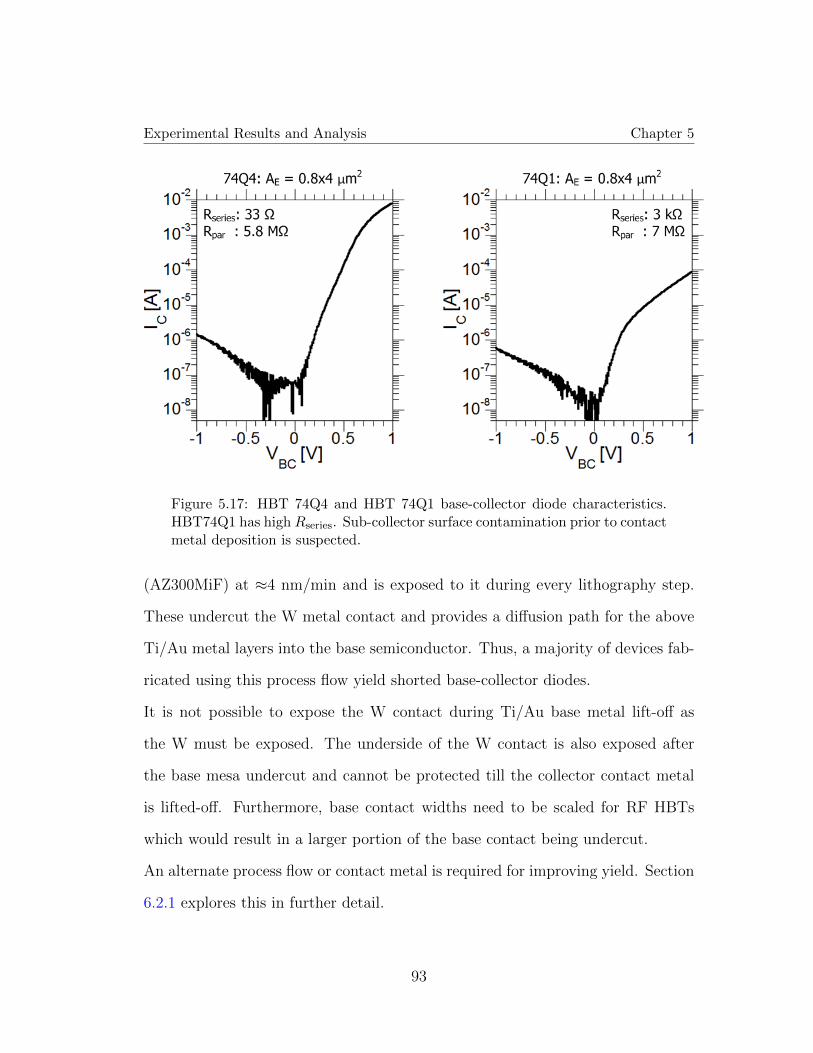
Experimental Results and Analysis Chapter 5
Figure 5.17: HBT 74Q4 and HBT 74Q1 base-collector diode characteristics.HBT74Q1 has high Rseries. Sub-collector surface contamination prior to contactmetal deposition is suspected.
(AZ300MiF) at ≈4 nm/min and is exposed to it during every lithography step.
These undercut the W metal contact and provides a diffusion path for the above
Ti/Au metal layers into the base semiconductor. Thus, a majority of devices fab-
ricated using this process flow yield shorted base-collector diodes.
It is not possible to expose the W contact during Ti/Au base metal lift-off as
the W must be exposed. The underside of the W contact is also exposed after
the base mesa undercut and cannot be protected till the collector contact metal
is lifted-off. Furthermore, base contact widths need to be scaled for RF HBTs
which would result in a larger portion of the base contact being undercut.
An alternate process flow or contact metal is required for improving yield. Section
6.2.1 explores this in further detail.
93

Experimental Results and Analysis Chapter 5
Figure 5.18: HBT74Q4 and HBT74Q1 gummel curves. The regrown-emitterHBT (74Q4) shows higher β of 28 as compared to 13 for 74Q1, at VCB=0. Itis unclear if this is due to higher RBE,series and lower RBC,series.
Figure 5.19: HBT 74Q4 and HBT 74Q1 common-emitter characteristics. 74Q1shows quasi-saturation as IB is increased.
94
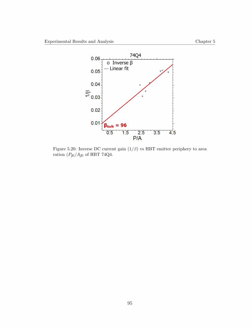
Experimental Results and Analysis Chapter 5
Figure 5.20: Inverse DC current gain (1/β) vs HBT emitter periphery to arearation (PjE/AjE of HBT 74Q4.
95
REFERENCES
References
[1] Noriyuki Watanabe, Shoji Yamahata, Takashi Kobayashi, Hydrogen removalby annealing from C-doped InGaAs grown on InP by metalorganic chemicalvapor deposition, Journal of Crystal Growth, Volume 200, Issues 34, April1999, Pages 599-602, ISSN 0022-0248
[2] L. J. van der Pauw, ”A Method of Measuring Specific Resistivity and HallEffect of Discs of Arbitrary Shapes,”. Philips Res. Repts. 13, 1-9 (1958).
[3] Ultralow resistance, nonalloyed Ohmic contacts to n-InGaAs Baraskar,Ashish K. and Wistey, Mark A. and Jain, Vibhor and Singisetti, Uttam andBurek, Greg and Thibeault, Brian J. and Lee, Yong Ju and Gossard, ArthurC. and Rodwell, Mark J. W., Journal of Vacuum Science and Technology B,27, 2036-2039 (2009)
[4] A. Baraskar, (Development of Ultra-Low Resistance Ohmic Contacts forInGaAs/InP HBTs.. PhD thesis. University of California, Santa Barbara,Santa. Barbara, Ca, U.S.A., 2011.
[5] Xing, H.; Jena, D.; Rodwell, M.J.W.; Mishra, U.K., ”Explanation of anoma-lously high current gain observed in GaN based bipolar transistors,” in Elec-tron Device Letters, IEEE , vol.24, no.1, pp.4-6, Jan. 2003
[6] V. Jain, InP DHBTs in a Refractory Emitter Process for THz Electronics..Ph.D. Thesis, University of California, Santa Barbara, Santa. Barbara, Ca,U.S.A., 2011.
[7] The Alloying of Gold and Gold Alloy Ohmic Contact Metallizations withGallium Arsenide. Miller, DC, J. Electrochem. Soc. 1980 127(2): 467-475
96
Chapter 6
Conclusion
6.1 Accomplishments
6.1.1 Improving RF HBT Design and Process
The yield in RF HBTs has been improved by developing and incorporating
a low temperature sputtered SiN layer post planarization (Section 3.1). This
anchors the high aspect ratio emitter metal and prevents shearing due to BCB
expansion in subsequent steps as the sample is heated.
An Iridium base contact process was developed and integrated into the RF
HBT process flow. Lower base contact resistivity to p-InGaAs has previously
been reported using Ir [1], and it has the added advantage of not sinking in
to the semiconductor [2]. An Al2O3/SiN composite sidewall was developed for
protecting the W/TiW emitter metal during blanket Ir etch in SF6/Ar. Initial
results were successful on test structures. The high power SF6/Ar etch has low
selectivity between Ir and the Al2O3/SiN composite sidewall. Thus, the etch
97

Conclusion Chapter 6
must be calibrated to prevent the emitter metal from being attacked. Tool drift
from sample to sample was observed which resulted in the emitter metal being
etched on RF HBT runs (Figure 3.3). HfO2 and ZrO2 ALD film etch selectivity
to SF6/Ar should be explored as sidewall dielectrics.
HBT epitaxial design was optimized to support maximum emitter current
density JE >40mA/µm2. HBT cutoff frequencies can be increased by increasing
emitter current density and thus reducing charging delays in the emitter-base and
base-collector junctions. The HBT epi must be designed for a specific collector
current density JC,Kirk. Due to collector current spreading, this is empirically
found to be half of JE [3]. Recent HBT designs show emitter starvation before
Kirk limit is reached [2] and thus the HBT epi structure must be redesigned. The
doping in the emitter space charge region has been increased, and its thickness
decreased in order to increase the base-emitter voltage at which base-pushout
occurs at the emitter-base junction [4].
The base epi design was optimized to reduce Auger recombination while main-
taining high doping at the emitter-base junction for low base contact resistivity.
Reducing base access resistance Rbb is crucial for increasing unity power gain
cutoff frequency fmax in HBTs. Base doping must be increased to reduce lat-
eral base resistance Rb,gap, Rb,spread, Rb,sh and base contact resistivity Rb,cont. [5].
However, Auger recombination in the base has a quadratic relation to the base
doping and must be accounted for in modern RF HBTs where the base doping
is > 1x1020cm−3 [6]. The base epi design must reduce Auger recombination as
well as Rbb. Previous base designs with a pulse doping for lower Rb,cont. [3] were
modified to a dual doping grade with the minimum doping in the top grade being
98
Conclusion Chapter 6
> 1 ∗ 1020cm−3 to ensure low contact resistivity. The dual grade introduces a
quasi-electric field in the heavily doped regions as well, thus reducing base transit
time and Auger recombination.
6.1.2 Process Development For WE < 100nm
A new process flow for scaling HBT emitter width (wE) below 100 nm by us-
ing ALD metal deposition is proposed and developed. Increasing HBT ft, fmax
requires a decrease in device dimensions and access resistances, and an increase
in JE. Reducing wE decreases emitter-base junction capacitance Cje, and emitter-
base diffusion capacitance Cdiff . The existing UCSB W/TiW dual refractory emit-
ter metal stack enables wE of 100 nm, but cannot scale further. A new process
flow has been developed where a high aspect ratio trench is etched into a sacrificial
Si film and is then filled with metal via ALD to form the emitter metal. Si is used
as the trench material since high aspect ratio trench processes in Si have been
demonstrated [8]. The process requires the trench width and sidewall profile to
be vertical for complete ALD metal fill in.
Emitters of wE < 70 nm have been successfully fabricated on test structures
using ALD TiN. TiN emitter HBTs suffer from open base-emitter junctions due
to interficial oxide formation on TiN. ALD Pt emitters could not be successfully
integrated into an HBT process flow as Pt etches in the blanket Si etch after
emitter metal deposition. ALD Ru is a viable alternative as it has high electrical
conductivity, low contact resistivity to n-InGaAs, can withstand high current
density without suffering from electromigration, and does not etch in the blanket
Si etch. The UCSB cleanroom has recently acquired an ALD tool capable of
99

Conclusion Chapter 6
depositing Ru thin films, which enables this.
6.1.3 MOCVD Selective Emitter Regrowth of HBT LADs
A process flow for selective regrowth of the emitter semiconductor has been
developed and Large Area Devices (LADs) fabricated. Theoretical calculations
for regrowth designs are presented which show an expected increase in DC cur-
rent gain β and cutoff frequencies. New epi designs are presented for regrowth
structures.
β of RF HBTs decreases with decreasing emitter width due to an increase inIB,edge
IB
andIB,Auger
IB. A regrown emitter structure allows for a thin, lightly doped intrinsic
base which reduces Auger recombination and base transit time to increase β and
ft respectively. The extrinsic base can be heavily doped to decrease Rb,cont. and
thus increase fmax. The extrinsic base also forms a barrier for electrons diffusing
towards the base contact which increases β.
MOCVD introduces H+ at high temperatures which passivates carbon dopants
in the p-InGaAs base. H+ can be removed and the carbon reactivated by anneal-
ing the samples in N2 at 500C for 10 min. This damages the p-InGaAs surface
and leads to prohibitively high base contact resistivity and sheet resistance. InP
and W based caps as a means of minimizing surface damage during regrowth and
anneal are presented. While in-situ grown InP is an effective regrowth cap, it must
be thin enough to be etched away via digital etch and not attack the regrown InP
emitter. W is an effective annealing cap, but insufficient as a regrowth cap due
to poor growth morphology and InGaAs void formation.
HBT LADs with MOCVD emitter regrowth have been fabricated using SiO2
100
Conclusion Chapter 6
and W as a regrowth and anneal cap respectively. They are compared with non-
regrowth LADs that were fabricated simultaneously. Maximum β of 28 and 13
was measured on regrowth and non-regrowth devices respectively, for emitters of
area 0.8x4 µm2. Regrowth emitter-base diodes show higher series resistance, thus
it is unclear if a higher β in the regrown-emitter HBT is due to lower IB,Auger
in the intrinsic base and lower IB,diff due to presence of extrinsic-intrinsic base
conduction band barrier. βbulk of 96 is extracted for regrown emitter devices.
The current process suffers from low yield due to lateral undercut of W base
contact in subsequent process steps. Yield can be improved by using alternate
refractory metal contacts such as Ru.
6.2 Future Work
6.2.1 Alternate Base Contact Technologies
Blanket W base contacts as annealing caps have yielded working HBT devices
with low Rb,cont. and Rb,sh. W acts as a barrier that prevents the InGaAs base
elements from diffusing out during the carbon reactivation anneal. However, W
is easily etched in subsequent process step chemistries which significantly lowers
device yield.
Ruthenium is a promising alternative to W. Low contact resistivity to p-
InGaAs using Ru as a contact metal has been demonstrated [1]. It is a refractory
metal that does not diffuse at annealing temperatures of >500C which also makes
it an excellent diffusion barrier against InGaAs elements. Moreover, Ru is inert
to most chemicals just like the other metals of the Platinum group.
101

Conclusion Chapter 6
Using Ru as a blanket base metal contact and annealing cap would significantly
improve device yield. The blanket metal can be dry etched in the field using
Cl2/O2 plasma, prior to the base mesa wet etch.
Ru integration into regrowth HBT process flow might present challenges in process
steps that require wet etches. Ru is a known versatile catalyst and it’s unknown
if its presence would lead to any side-effects.
It is also possible to incorporate Pt/Ru blanket base metal contacts that are
used in RF HBTs. They retain all the desirable properties of Ru contacts except
that the Pt reacts and sinks into the semiconductor. While RF HBTs show a metal
sinking depth of ≈3nm [2], the sinking depth after a 500C anneal is unknown.
6.2.2 Pulse InP Regrowth Cap
Using an in-situ InP cap for protecting the base surface during regrowth is
desirable as the p-InGaAs is not exposed till refractory base contact deposition.
The base metal can then be used as an annealing cap. A thick InP cap requires
a wet etch which also attacks the regrown InP emitter (Section 5.6.3). However,
a pulse InP cap (3nm) can be grown insitu, and then digitally etched without
attacking the InP emitter. This was not possible as existing RF HBT epi was
used to test the MOCVD emitter regrowth process. However, an epi designed
for regrowth can incorporate this feature which significantly reduces base surface
damage. No side-effects to this integration are expected.
102

Conclusion Chapter 6
6.2.3 Epitaxial Design For Emitter Regrowth
As mentioned in 5.3, the HBT epi used for MOCVD emitter regrowth was
initially designed for RF HBTs at the 100 nm emitter node. The emitter semi-
conductor was blanket wet etched away before deposition of the oxide regrowth
mask for emitter regrowth. This approach increased base surface damage due
to the oxide regrowth cap. The extrinsic base thickness was arbitrarily designed
based on digital etch thickness and it could not be made thicker without increas-
ing intrinsic base sheet resistance. Moreover, there was no doping step between
the intrinsic and extrinsic base that would create a diffusion barrier. The doping
grade in the base however generates a quasi-electric field that also inhibits electron
diffusion to the base contacts.
The focus of this work was to show feasibility of fabricating HBTs using
MOCVD selective emitter regrowth. HBT epi must be designed explicitly for
regrowth to demonstrate an increase in β and cutoff frequencies. Key new fea-
tures of a regrowth structure include a pulse InP cap above the base, doping step
at the extrinsic-intrinsic base boundary, thicker heavily doped extrinsic base, and
thinner lightly doped intrinsic base. The pulse InP cap reduces surface damage
and is discussed in 6.2.2. The doping step in the base induces a diffusion barrier
for electrons diffusing towards the base contact metal. A thicker and highly doped
extrinsic base allows for base metal sinking without affecting Rb,cont. Moreover,
the extrinsic base surface can now be digitally etched to remove damaged layers
before depositing metal contacts. Since the entire extrinsic base is heavily doped,
low Rb,cont is maintained. A sample epi design is shown in Table 6.1.
103
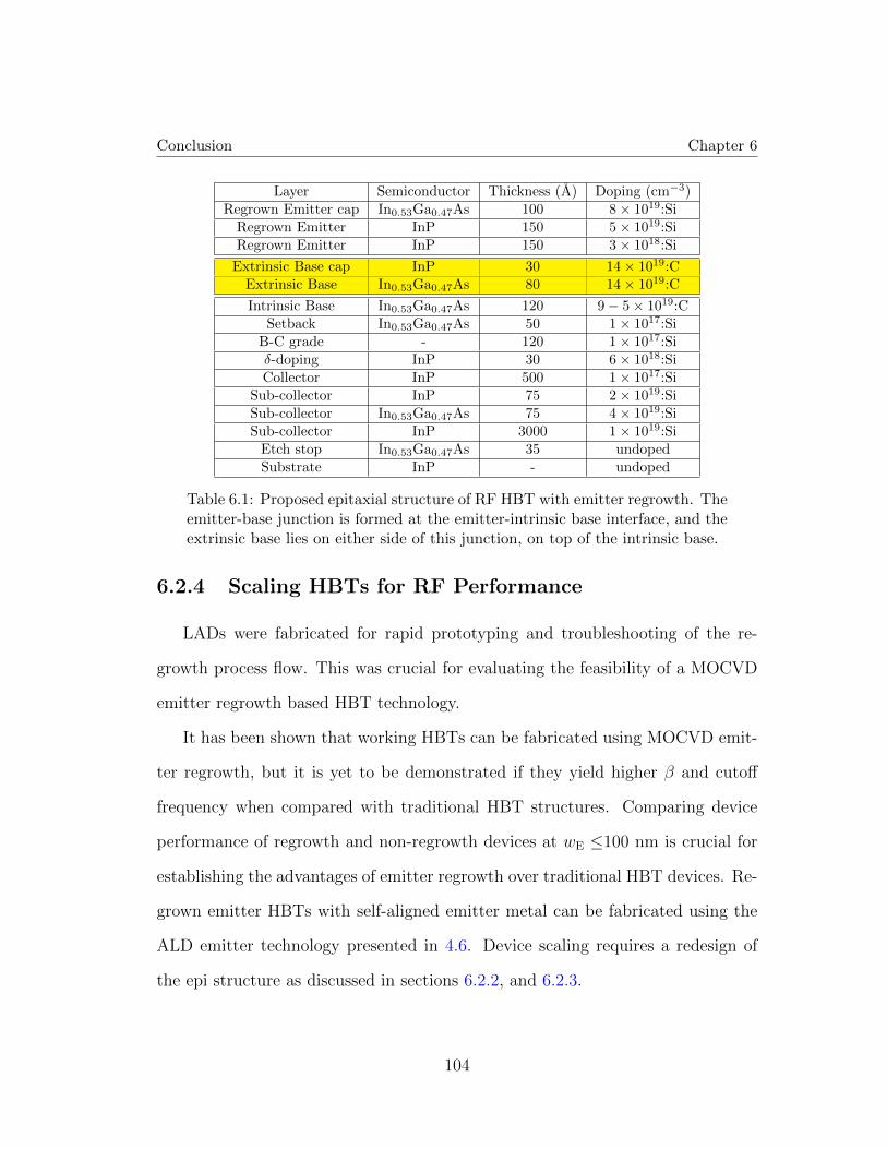
Conclusion Chapter 6
Layer Semiconductor Thickness (A) Doping (cm−3)Regrown Emitter cap In0.53Ga0.47As 100 8× 10¹⁹:Si
Regrown Emitter InP 150 5× 10¹⁹:SiRegrown Emitter InP 150 3× 10¹⁸:Si
Extrinsic Base cap InP 30 14× 1019:CExtrinsic Base In0.53Ga0.47As 80 14× 1019:C
Intrinsic Base In0.53Ga0.47As 120 9− 5× 10¹⁹:CSetback In0.53Ga0.47As 50 1× 10¹⁷:Si
B-C grade - 120 1× 10¹⁷:Siδ-doping InP 30 6× 10¹⁸:SiCollector InP 500 1× 10¹⁷:Si
Sub-collector InP 75 2× 10¹⁹:SiSub-collector In0.53Ga0.47As 75 4× 10¹⁹:SiSub-collector InP 3000 1× 10¹⁹:Si
Etch stop In0.53Ga0.47As 35 undopedSubstrate InP - undoped
Table 6.1: Proposed epitaxial structure of RF HBT with emitter regrowth. Theemitter-base junction is formed at the emitter-intrinsic base interface, and theextrinsic base lies on either side of this junction, on top of the intrinsic base.
6.2.4 Scaling HBTs for RF Performance
LADs were fabricated for rapid prototyping and troubleshooting of the re-
growth process flow. This was crucial for evaluating the feasibility of a MOCVD
emitter regrowth based HBT technology.
It has been shown that working HBTs can be fabricated using MOCVD emit-
ter regrowth, but it is yet to be demonstrated if they yield higher β and cutoff
frequency when compared with traditional HBT structures. Comparing device
performance of regrowth and non-regrowth devices at wE ≤100 nm is crucial for
establishing the advantages of emitter regrowth over traditional HBT devices. Re-
grown emitter HBTs with self-aligned emitter metal can be fabricated using the
ALD emitter technology presented in 4.6. Device scaling requires a redesign of
the epi structure as discussed in sections 6.2.2, and 6.2.3.
104

REFERENCES
References
[1] A. Baraskar, (Development of Ultra-Low Resistance Ohmic Contacts forInGaAs/InP HBTs.. PhD thesis. University of California, Santa Barbara,Santa. Barbara, Ca, U.S.A., 2011.
[2] J. Rode, IC Fabrication Technology for Highly Scaled THz DHBTs.. Ph.D.Thesis, University of California, Santa Barbara, Santa. Barbara, Ca, U.S.A.,2015.
[3] V. Jain, InP DHBTs in a Refractory Emitter Process for THz Electronics..Ph.D. Thesis, University of California, Santa Barbara, Santa. Barbara, Ca,U.S.A., 2011.
[4] Jain, V.; Rodwell, Mark J.W., ”Transconductance Degradation inNear-THz InP Double-Heterojunction Bipolar Transistors,” in ElectronDevice Letters, IEEE , vol.32, no.8, pp.1068-1070, Aug. 2011. doi:10.1109/LED.2011.2157451
[5] Rodwell, Mark J.W.; Urteaga, M.; Mathew, T.; Scott, D.; Mensa, Dino; Lee,Q.; Guthrie, J.; Betser, Y.; Martin, S.C.; Smith, R.P.; Jaganathan, S.; Kr-ishnan, S.; Long, S.I.; Pullela, R.; Agarwal, B.; Bhattacharya, U.; Samoska,L.; Dahlstrom, M., ”Submicron scaling of HBTs,” in Electron Devices, IEEETransactions on , vol.48, no.11, pp.2606-2624, Nov 2001
[6] H. Chiang, Design and Fabrication of Sub-100nm Base-Emitter Junctionsof THz InP DHBTs.. Ph.D. Thesis, University of California, Santa Barbara,Santa Barbara, Ca, U.S.A., 2014...
[7] . Lateral carrier diffusion and current gain in terahertz InGaAs/InP double-heterojunction bipolar transistors. Chiang, Han-Wei and Rode, Johann C.and Choudhary, Prateek and Rodwell, Mark J. W., Journal of AppliedPhysics, 115, 034513 (2014)
[8] Sub-50 nm high aspect ratio silicon pillars, ridges, and trenches fabricatedusing ultrahigh resolution electron beam lithography and reactive ion etching.Fischer, P. B. and Chou, S. Y., Applied Physics Letters, 62, 1414-1416 (1993)
105
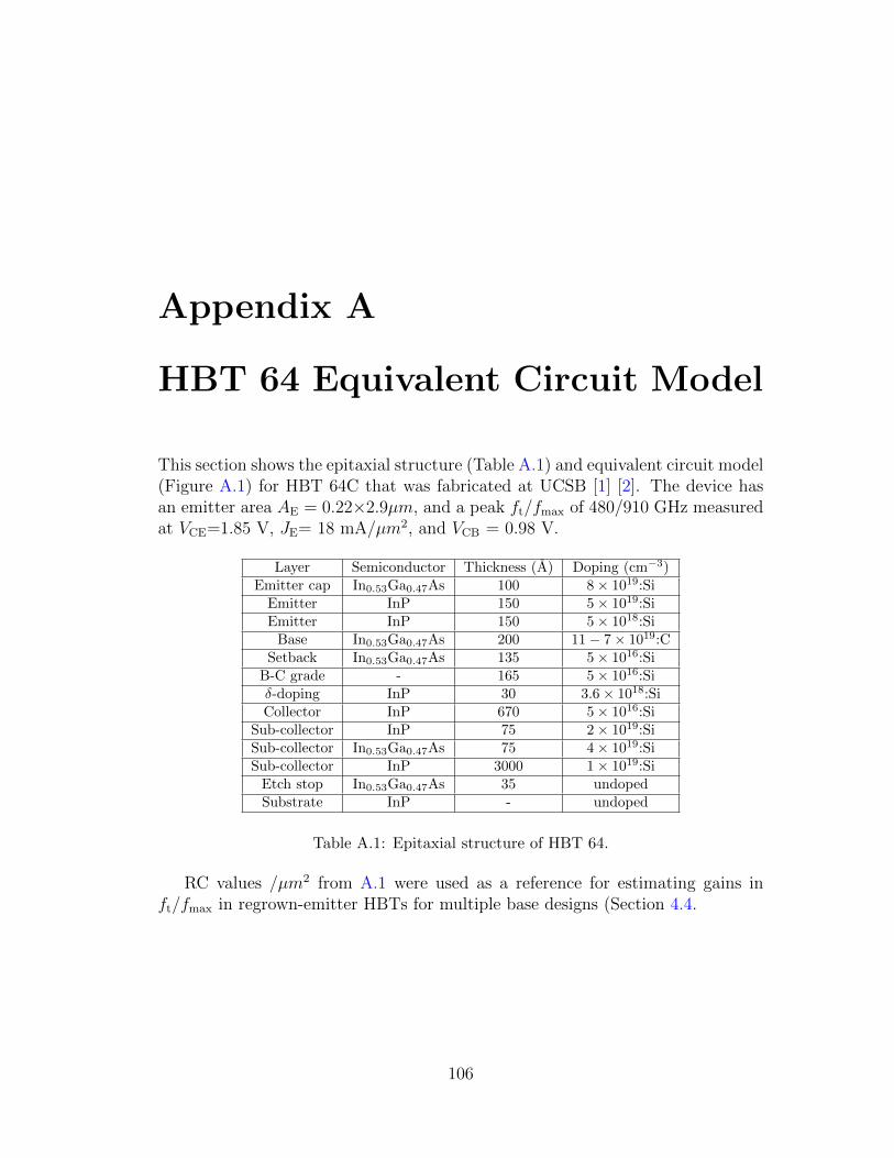
Appendix A
HBT 64 Equivalent Circuit Model
This section shows the epitaxial structure (Table A.1) and equivalent circuit model(Figure A.1) for HBT 64C that was fabricated at UCSB [1] [2]. The device hasan emitter area AE = 0.22×2.9µm, and a peak ft/fmax of 480/910 GHz measuredat VCE=1.85 V, JE= 18 mA/µm2, and VCB = 0.98 V.
Layer Semiconductor Thickness (A) Doping (cm−3)Emitter cap In0.53Ga0.47As 100 8× 10¹⁹:Si
Emitter InP 150 5× 10¹⁹:SiEmitter InP 150 5× 10¹⁸:Si
Base In0.53Ga0.47As 200 11− 7× 10¹⁹:CSetback In0.53Ga0.47As 135 5× 10¹⁶:Si
B-C grade - 165 5× 10¹⁶:Siδ-doping InP 30 3.6× 10¹⁸:SiCollector InP 670 5× 10¹⁶:Si
Sub-collector InP 75 2× 10¹⁹:SiSub-collector In0.53Ga0.47As 75 4× 10¹⁹:SiSub-collector InP 3000 1× 10¹⁹:Si
Etch stop In0.53Ga0.47As 35 undopedSubstrate InP - undoped
Table A.1: Epitaxial structure of HBT 64.
RC values /µm2 from A.1 were used as a reference for estimating gains inft/fmax in regrown-emitter HBTs for multiple base designs (Section 4.4.
106

Figure A.1: Equivalent circuit model of HBT 64C. AE = 0.22×2.9 µm2
107
References
[1] J. Rode, IC Fabrication Technology for Highly Scaled THz DHBTs.. Ph.D.Thesis, University of California, Santa Barbara, Santa. Barbara, Ca, U.S.A.,2015.
[2] Rode, J.C.; Chiang, H.-W.; Choudhary, P.; Jain, V.; Thibeault, B.J.;Mitchell, W.J.; Rodwell, M.J.W.; Urteaga, M.; Loubychev, D.; Snyder, A.;Wu, Y.; Fastenau, J.M.; Liu, A.W.K., ”An InGaAs/InP DHBT With Simul-taneous ft/fmax 404/901 GHz and 4.3 V Breakdown Voltage,” in ElectronDevices Society, IEEE Journal of the , vol.3, no.1, pp.54-57, Jan. 2015
108

Appendix B
UCSB W/TiW Emitter MetalProcess
This sections lists the process flow for the blanket sputtered W/TiW dry etchemitter process developed [1] [2] and optimized [3] [4] at UCSB, for InP/InGaAsHBTs of emitter width ≥100 nm. Figure B.1 shows the process flow.
109
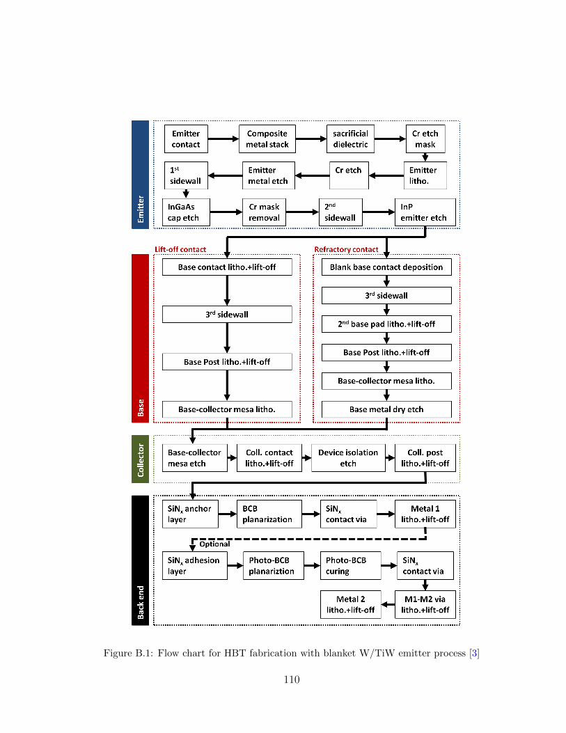
Figure B.1: Flow chart for HBT fabrication with blanket W/TiW emitter process [3]
110
References
[1] V. Jain, InP DHBTs in a Refractory Emitter Process for THz Electronics..Ph.D. Thesis, University of California, Santa Barbara, Santa. Barbara, Ca,U.S.A., 2011.
[2] E. Lobisser, Scaling Mesa InP DHBTs to Record Bandwidths.. Ph.D. Thesis,University of California, Santa Barbara, Santa. Barbara, Ca, U.S.A., 2011.
[3] H. Chiang, Design and Fabrication of Sub-100nm Base-Emitter Junctionsof THz InP DHBTs.. Ph.D. Thesis, University of California, Santa Barbara,Santa Barbara, Ca, U.S.A., 2014
[4] J. Rode, IC Fabrication Technology for Highly Scaled THz DHBTs.. Ph.D.Thesis, University of California, Santa Barbara, Santa. Barbara, Ca, U.S.A.,2015.
111


![MOCVD Emitter Regrowth Technology for Scaling InGaAs/InP … · DC Current Gain of 28, in progress for IEEE Electron Device Trans. (2015) [2] P. Choudhary, J.W. Holt, S. Kempf, D.](https://static.fdocuments.in/doc/165x107/5f19072c3d19901d7424a033/mocvd-emitter-regrowth-technology-for-scaling-ingaasinp-dc-current-gain-of-28.jpg)


