Selective area regrowth and doping for
28
Houqiang Fu 1,2, ⇑ ,† , Kai Fu 1,† , Chen Yang 1 , Hanxiao Liu 3 , Kevin A. Hatch 3 , Prudhvi Peri 4 , Dinusha Herath Mudiyanselage 2 , Bingjun Li 5 , Tae-Hyeon Kim 6 , Shanthan R. Alugubelli 3 , Po-Yi Su 3 , Daniel C. Messina 3 , Xuguang Deng 1 , Chi-Yin Cheng 1 , Reza Vatan Meidanshahi 1 , Xuanqi Huang 1 , Hong Chen 1 , Tsung-Han Yang 1 , Jingan Zhou 1 , Andrew M. Armstrong 7 , Andrew A. Allerman 7 , Edward T. Yu 6 , Jung Han 5 , Stephen M. Goodnick 1 , David J. Smith 3 , Robert J. Nemanich 3 , Fernando A. Ponce 3 , Yuji Zhao 1, ⇑ 1 School of Electrical, Computer, and Energy Engineering, Arizona State University, Tempe AZ, 85287 USA 2 Department of Electrical and Computer Engineering, Iowa State University, Ames, IA 50011, USA 3 Department of Physics, Arizona State University, Tempe, AZ 85287, USA 4 School for Engineering of Matter, Transport and Energy, Arizona State University, Tempe, AZ 85287, USA 5 Department of Electrical Engineering, Yale University, New Haven, CT 06511, USA 6 Department of Electrical and Computer Engineering, The University of Texas at Austin, Austin, TX 78758, USA 7 Sandia National Laboratories, Albuquerque, NM 87185, USA This paper reviews materials challenges and recent progress for selective area regrowth and doping for vertical gallium nitride (GaN) power devices. The purpose is to realize randomly placed, reliable, contactable, and generally useable laterally patterned p-n junctions, which are the building blocks for various advanced power rectifiers and transistors. The general regrowth process and regrowth dynamics in trenches were discussed, where the effects of trench geometries, growth methods, and bulk substrates were elucidated. Comprehensive materials characterization techniques were utilized to analyze the regrown structures, including scanning electron microscopy, transmission electron microscopy, atom probe tomography, scanning probe microscopy, and secondary-ion mass spectrom- etry. Cathodoluminescence and secondary electrons in scanning electron microscopy and atom probe tomography were used to achieve lateral and vertical dopant profiling at a sub-micron scale. The regrowth interface after dry etching accumulated a high density of impurities and charges, contribut- ing to the formation of a p + -n + tunneling junction. This hypothesis was further confirmed by the electrostatic potential profile at the regrowth interface using electron holography. Novel etching technologies were investigated to improve the regrowth interface. It was found that low-power dry etching significantly reduced the interfacial charges and the reverse leakage currents of regrown p-n junctions. Photoelectrochemical wet etching was found to be effective in reducing deep-level defects near the regrowth interface. Atomic layer etching uses self-limiting chemical processes, thus removing Selective area regrowth and doping for vertical gallium nitride power devices: Materials challenges and recent progress ⇑ Corresponding authors. E-mail addresses: Fu, H. ([email protected]), Zhao, Y. ([email protected]). † The two authors contributed equally to this work. 1369-7021/Ó 2021 Elsevier Ltd. All rights reserved. https://doi.org/10.1016/j.mattod.2021.04.011 1 Materials Today d Volume xxx, Number xx d xxxx 2021 RESEARCH RESEARCH: Review Please cite this article in press as: H. Fu et al., Materials Today, (2021), https://doi.org/10.1016/j.mattod.2021.04.011
Transcript of Selective area regrowth and doping for

Materials Today d Volume xxx, Number xx d xxxx 2021 RESEARCH
Selective area regrowth and doping for
EARCH:Rev
iew
vertical gallium nitride power devices:
Materials challenges and recent progress RES
Houqiang Fu 1,2,⇑,†, Kai Fu 1,†, Chen Yang 1, Hanxiao Liu 3, Kevin A. Hatch 3, PrudhviPeri 4, Dinusha Herath Mudiyanselage 2, Bingjun Li 5, Tae-Hyeon Kim 6, Shanthan R.Alugubelli 3, Po-Yi Su 3, Daniel C. Messina 3, Xuguang Deng 1, Chi-Yin Cheng 1, RezaVatan Meidanshahi 1, Xuanqi Huang 1, Hong Chen 1, Tsung-Han Yang 1, JinganZhou 1, Andrew M. Armstrong 7, Andrew A. Allerman 7, Edward T. Yu 6, Jung Han 5,Stephen M. Goodnick 1, David J. Smith 3, Robert J. Nemanich 3, Fernando A. Ponce 3,Yuji Zhao 1,⇑
1 School of Electrical, Computer, and Energy Engineering, Arizona State Univ
ersity, Tempe AZ, 85287 USA2Department of Electrical and Computer Engineering, Iowa State University, Ames, IA 50011, USA3Department of Physics, Arizona State University, Tempe, AZ 85287, USA4 School for Engineering of Matter, Transport and Energy, Arizona State University, Tempe, AZ 85287, USA5Department of Electrical Engineering, Yale University, New Haven, CT 06511, USA6Department of Electrical and Computer Engineering, The University of Texas at Austin, Austin, TX 78758, USA7 Sandia National Laboratories, Albuquerque, NM 87185, USAThis paper reviews materials challenges and recent progress for selective area regrowth and doping forvertical gallium nitride (GaN) power devices. The purpose is to realize randomly placed, reliable,contactable, and generally useable laterally patterned p-n junctions, which are the building blocks forvarious advanced power rectifiers and transistors. The general regrowth process and regrowthdynamics in trenches were discussed, where the effects of trench geometries, growth methods, andbulk substrates were elucidated. Comprehensive materials characterization techniques were utilized toanalyze the regrown structures, including scanning electron microscopy, transmission electronmicroscopy, atom probe tomography, scanning probe microscopy, and secondary-ion mass spectrom-etry. Cathodoluminescence and secondary electrons in scanning electron microscopy and atom probetomography were used to achieve lateral and vertical dopant profiling at a sub-micron scale. Theregrowth interface after dry etching accumulated a high density of impurities and charges, contribut-ing to the formation of a p+-n+ tunneling junction. This hypothesis was further confirmed by theelectrostatic potential profile at the regrowth interface using electron holography. Novel etchingtechnologies were investigated to improve the regrowth interface. It was found that low-power dryetching significantly reduced the interfacial charges and the reverse leakage currents of regrown p-njunctions. Photoelectrochemical wet etching was found to be effective in reducing deep-level defectsnear the regrowth interface. Atomic layer etching uses self-limiting chemical processes, thus removing
⇑ Corresponding authors.
E-mail addresses: Fu, H. ([email protected]), Zhao, Y. ([email protected]).† The two authors contributed equally to this work.
1369-7021/� 2021 Elsevier Ltd. All rights reserved. https://doi.org/10.1016/j.mattod.2021.04.0111
Please cite this article in press as: H. Fu et al., Materials Today, (2021), https://doi.org/10.1016/j.mattod.2021.04.011

RESEA
RCH:R
eview
RESEARCH Materials Today d Volume xxx, Number xx d xxxx 2021
the damaged layers without inducing further etching damage. Tertiarybutylchloride-based in situetching may serve as an alternative etching method to dry etching with reduced etching damage. Interms of devices, regrown p-n junctions with low leakage currents and vertical junction field-effecttransistors were demonstrated. Further improvements in selective area regrowth and associated devicescan be expected using regrowth optimization and regrowth interface engineering via surfacetreatments and low-damage etching. These results represent an important step towards realizingselective area regrowth and doping for high performance GaN power electronics devices and systems.
Keywords: Gallium nitride; Power electronics; Vertical power devices; Selective area doping and regrowth; interface
engineeringIntroductionWide bandgap semiconductor gallium nitride (GaN) has beenextensively researched as the emerging workhorse for the next-generation efficient power electronic devices and systems dueto its wide bandgap, high critical electric field, fast switchingspeed, and high Baliga’s figure of merit [1–12]. Fig. 1a comparesthe performance of different semiconductors for power electron-ics applications, where GaN devices are expected to outperformtheir Si counterparts. In order to unleash the full potential ofGaN, vertical GaN power devices grown on bulk GaN substrates(Fig. 1b) have been widely investigated in recent years, includingSchottky barrier diodes [13–21], p-n diodes [22–42], otheradvanced power rectifiers [43–47] and transistors [48–58] suchas current aperture vertical electron transistors (CAVETs), trenchmetal–oxidesemiconductor field-effect transistors (MOSFETs),and fin field-effect transistors (FinFETs). In the early stage ofGaN power devices development, lateral devices such as theGaN high electron mobility transistors (HEMTs) were first pro-posed and demonstrated usually on foreign substrates such assapphire and SiC. In lateral devices, the current flows laterally,and the breakdown voltage is held laterally. Compared with lat-eral devices, vertical devices can offer tremendous advantages,including higher voltages, higher currents, smaller chip area, bet-ter thermal management, no surface-related issues, and ava-lanche capability [1,2,7]. However, one of the most criticalbuilding blocks that is still missing for vertical GaN powerdevices is laterally patterned GaN p-n junctions, the schematicof which is illustrated in Fig. 2a. These laterally patterned p-njunctions are the basis for many advanced GaN power devicesand edge terminations, such as vertical junction field-effect tran-sistors (VJFETs) (Fig. 2b), junction termination extension (JTE)(Fig. 2c), and junction barrier Schottky (JBS) or merged pn/Schot-tky (MPS) diodes (Fig. 2d).
Laterally patterned p-n junctions (Fig. 2a) can be realized byselective area doping via two methods: ion-implantation and epi-taxial regrowth. After decades of development, ion implantationhas become a mature technology in Si and SiC [59–61], and sim-ilar Si and SiC structures and devices to those in Fig. 2 have beendemonstrated. However, ion implantation still remains one ofthe biggest hurdles for GaN power devices [16]. This is mainlyattributed to the following reasons. Ion bombardment duringthe ion implantation process can cause severe material damage,and subsequent high temperature annealing (usually >1000 �C)is required to recover the damage. In addition, some of theimplanted atoms may be at interstitial sites, and high tempera-
2
Please cite this article in press as: H. Fu et al., Materials Today, (2021), https://doi.org/10.1
ture annealing can restore them to the correct substitutional sitesto activate them as dopants [61,62]. However, the high tempera-ture annealing can decompose GaN when above 900 �C andcause killer defects and surface degradation [63,64]. Severalmethods have been proposed to alleviate GaN decompositionat high temperatures, including AlN capping layers, multicyclerapid thermal annealing, and ultra-high annealing pressure[65–67]. Furthermore, the conductivity of implanted p-GaN isstill much lower than the epitaxially grown p-GaN [26,43],which can adversely impact device performance.
Epitaxial regrowth or selective area regrowth is regarded as apromising alternative route to realizing laterally patterned GaNp-n junctions. However, regrown GaN p-n junctions usually suf-fer from high leakage currents and low breakdown voltages[68,69]. In this review, challenges and recent progress of selectivearea regrowth and doping for vertical GaN power transistors arepresented. This review is organized as follows. Section 2 will dis-cuss the general regrowth process and the regrowth dynamics intrenches with two growth modes revealed. The effects of trenchgeometries, growth methods, and bulk substrates will be dis-cussed. Section 3 will focus on several important material charac-terization techniques for the selective area regrowth, includingcathodoluminescence (CL), dopant profiling via secondary elec-trons (SEs) in scanning electron microscopy (SEM), atom probetomography (APT), the regrowth interface characterizationsusing capacitance–voltage (C–V) measurements, secondary ionmass spectrometry (SIMS) and transmission electron microscopy(TEM), and electron holography and scanning probe microscopy(SPM) for the electrostatic potential profile at the regrowth inter-face. These techniques serve as the foundation for the regrowthstudy. Section 4 will introduce three novel etching technologiesto reduce etching damage or replace the state-of-the-art dry etch-ing method, including low-power dry etching, photoelectro-chemical (PEC) wet etching, atomic layer etching (ALE), andin situ and selective area etching. The effects of these etchingmethods on the performance of regrown devices will be dis-cussed. Section 5 will show several demonstrated regrowndevices, including planar regrown p-n junctions and the verticaljunction field-effect transistors (VJFETs).
Selective area regrowthRegrowth processIn order to achieve selective area doping by regrowth, dry etch-ing is an inevitable process to form the selective regions/trenchesfor regrowth. However, the etch-then-regrow process is very
016/j.mattod.2021.04.011

FIGURE 1
(a) Benchmark plot of specific on-resistance versus breakdown voltage for different semiconductors for power electronics applications. (b) Schematic ofvertical GaN power devices on bulk GaN substrates, including channel/contact layer, edge termination (ET), drift layer, and buffer layer.
RES
EARCH:Rev
iew
FIGURE 2
(a) Schematics of laterally patterned p-n junctions by selective area doping. (b) Vertical junction field effect transistors (VJFETs); (c) Junction terminationextension (JTE); (d) Junction barrier Schottky (JBS) or merged pn/Schottky (MPS) diodes.
Materials Today d Volume xxx, Number xxx d xxxx 2021 RESEARCH
challenging and induces interface impurities. Even without anyetching, the regrowth process still introduces a high concentra-tion of impurities at the regrowth interface, such as silicon (Si),carbon (C), and oxygen (O). Thermal desorption of these impu-rities through annealing in metal–organic chemical vapor depo-sition (MOCVD) or molecular beam epitaxy (MBE) has been usedfor in situ cleaning. Annealing in NH3 at 700–800 �C or multi-step alternating growth and annealing under vacuum at 780 �Ccould effectively remove C and O [70,71]. However, the residualSi was not able to be removed by these methods. These impuri-ties may not be a problem for regrowing n-type GaN since Siand O are shallow donors for n-type doping. However, theseimpurities are highly undesired for regrowing p-GaN since theycan compensate acceptors and reduce hole concentrations. Fur-thermore, the dry etching process can also introduce etchingdamage at the regrowth interface, causing deep-level defect/trapstates. Due to these issues, regrown GaN p-n junctions have suf-fered from high leakage and premature breakdown.
Please cite this article in press as: H. Fu et al., Materials Today, (2021), https://doi.org/10.1
Fig. 3a shows a typical regrowth process in MOCVD, includingthree steps, i.e., before regrowth, ramp-up with temperatures andgases, and regrowth. An n+-GaN buffer layer and an unintention-ally doped (UID) GaN were first grown on GaN substrates. Thenthe sample was taken out of the reactor for processing and thenreloaded into the reactor. To study the effect of growth conditionson the regrowth process, four different combinations of growthgases were used for the ramp-up step, including N2/NH3/H2, N2,N2/trimethylgallium (TMGa, 6 sccm), and N2/TMGa (12 sccm).Then a UID-GaN layer was regrown on top of the sample. Fig. 3bshows the SIMS profiles of the regrown UID-GaN with differentgases in the ramp-up step. Si peaks were observed in all samples.Although Ga-rich condition is helpful to reduce Si incorporation[72], the introduction of TMGa in the ramp-up step led to a signif-icant increase in Si, O, and C. Compared with other conditions,the sample under the N2/NH3/H2 showed the lowest Si concentra-tion at the regrowth interface. It has been reported that reducingthe sample’s exposure time to air can reduce the residual Si, for
3
016/j.mattod.2021.04.011

FIGURE 4
Top: SEM image of selective area regrowth in a trench. Bottom: Schematics of the thickness distribution of regrown p-GaN in different regions: trench,sidewalls, and mesa. The arrows indicate growth directions.
RESEA
RCH:R
eview
FIGURE 3
(a) Schematic of the regrowth process for regrown UID-GaN in MOCVD. (b) SIMS profile of the regrown UID-GaN with different ambient gases during theramp-up step.
RESEARCH Materials Today d Volume xxx, Number xx d xxxx 2021
example, putting the sample inN2 boxduringprocessing [73]. Sur-face treatment and etching conditions before regrowth are alsoimportant factors that can affect the interfacial impurity concen-
4
Please cite this article in press as: H. Fu et al., Materials Today, (2021), https://doi.org/10.1
tration, which will be discussed in the following sections. Overall,the residual Si at the interface is still an intractable issue forregrowth, and its origin is still unclear.
016/j.mattod.2021.04.011

FIGURE 5
SEM images of selective area regrowth in trenches with different widths. (a) 35 mm; (b) 25 mm; (c) 15 mm; (d) 9 mm; (e) 7 mm; (f) 5 mm.
FIGURE 6
Comparison of SE images and monochromatic CL mappings for different luminescent energies (3.4 eV, 3.25 eV, and 2.9 eV) for selective area regrowth intrenches with trench widths of 5 mm (left) and 9 mm (right). The right sample is slightly tilted so that part of the surface is also in view. SE: secondary electron.Reprinted from Ref. [79], with the permission of AIP Publishing.
RES
EARCH:Rev
iew
Materials Today d Volume xxx, Number xxx d xxxx 2021 RESEARCH
Regrowth on trench structuresThe laterally patterned p-n junctions were grown on n+-GaN sub-strates by MOCVD via an etch-then-regrow process. First, a UID-GaN layer was grown on the substrate. Then, the samples wereunloaded from the MOCVD reactor, and trenches were formedby inductively coupled plasma (ICP) etching. Finally, the sam-ples were reloaded into the MOCVD reactor, and p-GaN wasregrown. It should be noted that this process is a masklessregrowth process since previous studies showed that regrowth
Please cite this article in press as: H. Fu et al., Materials Today, (2021), https://doi.org/10.1
with SiO2 or Si3N4 masks resulted in the introduction of uninten-tional impurities such as Si or O and led to n-type conductivity[74–76]. Fig. 4 shows a representative SEM image of regrown p-GaN in a trench. The p-GaN appeared bright, and the n-GaNhad dark contrast; the reasons for this contrast difference arediscussed later [77]. The regrowth of p-GaN in the trench wasnonuniform. The p-GaN on the trench sidewall was muchthicker than other regions due to the faster lateral growth com-pared with the basal plane growth. This larger growth rate could
5
016/j.mattod.2021.04.011

FIGURE 7
Lateral growth versus vertical growth in p-GaN regrown on trenches. (a)Schematic cross-section showing the two characteristic regions observed inthe CL image with a 32� boundary, with p-GaN growth parallel to the basalplane and p�-GaN growth from the sidewall. (b) The atomic arrangement ofthe lattice indicating the 32� boundary for coincident lateral growth on0111
� �facets and on 0001f g basal planes. Reprinted from Ref. [79], with
the permission of AIP Publishing.
RESEA
RCH:R
eview
RESEARCH Materials Today d Volume xxx, Number xx d xxxx 2021
result in much lower Mg or acceptor concentrations in thesidewall.
To clarify the growth dynamics, selective area regrowth wasperformed in trenches with different trench widths and depths.With decreasing trench width, the thickness of the regrown p-GaN became more uniform throughout the trench, as shownin Fig. 5. For a trench width of < 9 mm, the p-GaN region in thetrench was rather flat. This is because, in a narrow trench, thegrowth fronts from the trench sidewall and the basal plane cancoalesce faster and form a united growth front, leading to uni-form p-GaN growth. Cathodoluminescence (CL) was used tomap the Mg distribution in the trenches. It has been identifiedthat strong CL emission at 2.9 eV is a reliable indicator for highacceptor concentrations [78]; more details on this topic are dis-cussed later. In the 2.9-eV CL mapping (Fig. 6), the central regionof the trench was much brighter than the sidewall [79], indicat-ing that the acceptor concentration in the former was higher.With increasing trench width, the central region of the trenchbecame brighter, which suggested that the basal plane growthwas becoming more dominant.
Understanding of the physical basis for these observationswas obtained by considering the lateral growth from the sidewalland the vertical growth from the basal plane of the trench [79].Surface steps of the growth front and their aggregation intosupersteps lead to a competition between step flow that resultsfrom the growth on microfacets and vertical growth from basalplanes [80]. Monochromatic CL images show that growth on
6
Please cite this article in press as: H. Fu et al., Materials Today, (2021), https://doi.org/10.1
basal planes exhibited a strong 2.9 eV emission, while growthfrom the sidewall facets did not [81]. The interface between theseregions formed an angle of about 32� with the basal plane, as
shown in the lattice structure in Fig. 7 [79]. The 0111� �
and
0001f g facets are the most stable in GaN and have been observedin epitaxial lateral overgrowth studies [82]. The sidewall facet canbe thought of as a highly tilted facet composed of a high densityof basal-plane steps, where each step serves as an effective site foradatom capture and facilitate lateral growth. The presence of Mg
on the 0111� �
facet can increase the adsorption of Ga and pro-
mote the accumulation of Ga adatoms in the vicinity of the side-wall. The lateral growth rate was found to be two times largerthan the vertical growth rate. Therefore, with the same amountof Mg acceptors available during growth, the acceptor concentra-tion near the sidewall will be smaller than that at the centralregion of the trench. This is confirmed by the CL analysis, inwhich the vertical growth region was p-type, while the lateralgrowth region was semi-insulating with a low acceptor concen-tration. In addition, previous studies also showed that Mg incor-poration efficiency was different on different facets.[78,81]Overall, the trench width must be optimized (not too wide nortoo narrow) (1) to ensure uniform p-GaN thickness inside thetrenches, and (2) to maximize basal plane growth to obtain thehighest acceptor concentrations in the trenches of the regrownp-GaN.
The effect of trench depth on selective area regrowth was alsoinvestigated, as shown in Fig. 8. For a shallow trench with adepth of 0.3 mm, no clear evidence of lateral growth from thesidewall was found by CL mapping. As the trench depthincreased, the sidewall surface area also increased. As a result,the area of lateral growth with low acceptor concentrations alsoincreased, as confirmed by the reduced CL emission intensity at2.9 eV near the sidewall. In addition, Fig. 9a shows that thereverse current leakage of the selective area doped p-n junctionsalso increased with increasing trench depth. The model shown inFig. 9b was proposed to explain this trend. According to the CLresults, the sidewall in deeper trenches had a lower acceptor con-centration, resulting in a p�-GaN or even intrinsic region. There-fore, the junction barrier near the sidewall may be reduced,creating a leakage path. This issue may be solved by adjustingthe growth mode or by increasing the acceptor doping or activa-tion efficiency along the sidewall. In short, using shallowtrenches for selective area growth may be beneficial for reducingthe reverse leakage of the selective area doped p-n junctions.
MOCVD and MBE regrowth comparisonMOCVD growth of GaN is typically performed at high tempera-tures (>950 �C) with NH3 as the precursor for N. There are signif-icant challenges, however, when the device structure involves p-GaN buried by subsequent n-GaN growth, such as current aper-ture vertical electron transistors (CAVETs) [1,2], trench-MOSFETs [48–53], and tunnel junctions (TJs) [83]. P-type con-ductivity of buried p-GaN is often hindered because active Hatoms from the decomposition of NH3 or H2 in n-GaN growthare able to diffuse backward and passivate Mg dopants whengrowing n-GaN under high temperatures [84]. After growth, acti-vation of the buried p-GaN becomes difficult due to a high diffu-
016/j.mattod.2021.04.011

RES
EARCH:Rev
iew
FIGURE 8
SE images and monochromatic CL mapping for different luminescent energies (3.4 eV, 3.25 eV, and 2.9 eV) for selective area regrowth in trenches withdifferent depths (0.3 mm, 1.4 mm, and 2.5 mm). The circled regions indicate the sidewall.
FIGURE 9
(a) Reverse leakage characteristics for selective-area doped p-n junctions with different trench depths. (b) A proposed model to explain the reverse leakage ofselective-area doped p-n junctions. The p-contacts are Pd/Ni/Au, and the n-contacts are Ti/Al/Ni/Au.
Materials Today d Volume xxx, Number xxx d xxxx 2021 RESEARCH
sion barrier of H atoms in the n-GaN [85]. Attempts have beenmade to activate buried p-GaN laterally through mesa sidewalls[86]. Moreover, Mg in the buried p-GaN can diffuse into the over-layers, which could adversely affect the properties of two-dimensional electron gas (2DEG) in the CAVET like structures.Similarly, defects generated during the ion-implantation processto form the current blocking layer (CBL) in CAVET structure werealso reported to diffuse to the active region and cause the currentcollapse in the on-state of operation [2].
MBE growth of GaN is carried out in a hydrogen-free environ-ment and is expected to provide solutions to the problems men-tioned above. MBE overgrowth on MOCVD-grown Mg-dopedGaN left the p-GaN remaining activated [87]. MBE-regrowntrench-MOSFET [88,89] and PolarMOS have been demonstrated
Please cite this article in press as: H. Fu et al., Materials Today, (2021), https://doi.org/10.1
[90]. Additionally, MBE employs much lower growth tempera-tures (<800 �C), which alleviates the diffusion of Mg atoms andpoint defects to active regions. Chowdhury et al. reporteddispersion-free CAVET structures with Mg implantation andMBE-regrown channels [2]. In addition, MBE-regrown p-n junc-tions showed a breakdown voltage of 1.1 kV, a specific on-resistance of 3.9 mO�cm2, and a turn-on voltage of 3.9 V [91].In these MBE regrown devices, the less-than-ideal deviceperformance was mainly due to defects and interface charges atthe regrowth interfaces [88–91].
In order to achieve non-planar or lateral p-n junction devices,selective area growth and doping is a very promising approach,as mentioned above. Selective area regrowth of GaN using MBEreactor has been reported by several groups. Different mask
7
016/j.mattod.2021.04.011

RESEA
RCH:R
eview
RESEARCH Materials Today d Volume xxx, Number xx d xxxx 2021
materials have been tested, including Ti, SiO2, and SiNx [92–94].High growth temperatures and low V/III ratios facilitated the des-orption of Ga atoms on the mask [93,94] and improved the selec-tivity. Good selectivity and surface morphology were onlyachieved on a periodic array of nanocolumn structures. Thelow V/III condition led to a porous surface morphology at hightemperatures for large-area devices [92]. Additionally, spike-likestructures at the edge of masks were observed due to the shortdiffusion length of adatoms [90,95].
Effects of bulk substratesRecent developments in crystal growth techniques such ashydride vapor pressure epitaxy (HVPE) and ammonothermalmethods have led to the availability of bulk GaN substrates withdefect densities lower than �106 cm�2. The recent developmentof bulk GaN substrates via the two methods is described in [96].HVPE GaN substrates are commercially available up to 4 inch.They are produced by growing thick GaN epilayers on foreignsubstrates such as sapphire and use the thick GaN epilayers asthe template for the next growth via an iterative fashion toimprove crystal quality. Ammonothermal GaN substrates are cur-rently only available mostly in 1 inch and up to 2 inch. But theyhave better crystal quality than HVPE substrates since they aregrown from single-crystal GaN seed via a melt approach. In addi-tion, Raghothamachar et al. [97] and Liu et al. [98] used syn-chrotron X-ray topography (XRT) to study the dislocations inthe HVPE and ammonothermal GaN substrates. They found thatHVPE substrates showed a heterogeneous distribution of disloca-tions that contained low threading dislocation areas betweenstrain centers with high threading dislocation densities. On theother hand, ammonothermal substrates had a much lower defectdensity than HVPE substrates. They were dominated by thread-ing mixed dislocations but free of basal plane dislocations. Epi-taxial GaN layers can be grown with much reduced defectdensity using such bulk substrates [99], and have enabled thefabrication of vertical GaN devices with high breakdown voltages[100]. Nevertheless, the occurrence of random defects is stillliable to cause degraded device performance and irreproducibledevice behavior. Since such defects cannot be totally eliminated,fabrication of devices for high power applications should con-centrate on areas with minimal defects and avoid regions withhigh defect densities in order to minimize defect-related currentleakage and possible device breakdown. The substrate morphol-ogy has a critical influence on the subsequent layer quality andthe corresponding device performance.
Fig. 10a–c compares XRT images of GaN thin films that weregrown on HVPE GaN substrates from two different sources andone grown on an ammonothermal substrate. The XRT image ofGaN grown on HVPE substrate-1 showed discontinuous, mostlyvertical features, whereas the XRT image of GaN grown on HVPEsubstrate-2 showed a two-dimensional array of dark spots. Inboth cases, the surface features were roughly equally spaced withlateral separations of �1 mm. In comparison, the XRT image ofGaN grown on the ammonothermal substrate revealed no signif-icant surface features. One of the GaN layers grown on HVPEsubstrate-2 was surface etched with ICP plasma, and SEM imagesrevealed micron-scale defects in the form of inverted hexagonal-pyramid pits at the locations of each dark spot. In contrast, areas
8
Please cite this article in press as: H. Fu et al., Materials Today, (2021), https://doi.org/10.1
away from these defective regions showed no visible flaws. Indevice studies, devices that overlapped with the dark spots per-formed poorly, whereas devices fabricated away from theseregions generally had much better performance. In marked con-trast, not all devices fabricated on the ammonothermal substrateperformed well. Fig. 10d shows several locations where deviceswere fabricated on the ammonothermal GaN substrate. The redcircles indicate locations of fabricated devices that had low break-down voltages, whereas the white circles indicate the areas ofdevices having typical high breakdown voltages. Fig. 10e showsa plan-view SEM image of such a device showing significant sur-face damage after breakdown, while Fig. 10f shows a device with-out visible surface damage after being stressed to high reversebiases. Overall, the HVPE-grown substrates showed surface fea-tures in XRT images that clearly should be avoided during devicefabrication. Conversely, the absence of any observable surfacefeatures for the ammonothermal substrates makes it challengingto predict device behavior. Furthermore, most of the currentselective area regrowth work is based on HVPE GaN substratesdue to their relatively early commercial availability. Future workis ongoing to study how the crystal conditions of bulk GaN sub-strates affect the selective area growth.
Materials characterizationMaterials characterization techniques play a critical role in selec-tive area regrowth and doping. They provide powerful tools toguide optimization in the design and growth and to understandthe performance of regrown GaN devices. In this section, severalmaterials characterization techniques that are instrumental toselective area regrowth and doping are discussed, including CLfor the acceptor distribution in mesa structures, dopant profilingvia SEs and ATP for both lateral and vertical structure at the sub-micron scale, regrowth interface study by C–V measurements,SIMS and TEM for interfacial charges and impurities, and elec-tron holography and SPM for electrostatic potential profiles atthe regrowth interfaces. These methods reveal materials chal-lenges in selective area regrowth and doping and physical mech-anisms for large leakage currents in regrown devices and providea route for future improvements.
CathodoluminescenceFig. 11a shows a typical growth and fabrication process to producelaterally patternedGaNp-n junctions. There are two growth direc-tions involved: thebasalplanegrowthontheupperandlowermesaflat regions and lateral growth on inclined crystal planes on themesa sidewall. It has been reported that crystal orientations inGaN significantly affect acceptor incorporation efficiency [101–103].Thus,itisessentialtohaveagoodunderstandingontheaccep-tor distribution in themesa structure. For example, inGaNVJFETs,the acceptor concentration in thep-GaNgate determines theoper-ation of devices, in particular, whether the gate can pinch off thechannel at zero bias. The traditional SIMSmethod cannot give reli-ablechemicalanalysisonthisstructureduetoits limitedlateral spa-tial resolution. Liu et al. [78] used CL spectroscopy to study opticalpropertiesofregrownp-GaNovermesastructuresatthesub-micronscale and their correlation with acceptor concentrations and elec-tronic properties. The CL was carried out in a JEOL 6300 SEM
016/j.mattod.2021.04.011

RES
EARCH:Rev
iew
FIGURE 10
XRT images from three different types of bulk GaN substrates: (a) GaN film on HVPE- substrate-1 showing the presence of dark discontinuous lines; (b) GaNfilm on HVPE substrate-2 showing a two-dimensional array of dark spot-like features; and (c) GaN film on ammonothermal substrate not showing anynoticeable surface features. (d) XRT image showing locations of fabricated devices, as marked by circles: red circles represent device locations having lowbreakdown voltages; white circles represent device locations having high breakdown voltages. (e) Plan-view SEM image of device marked as ‘A’ in (d),showing substantial surface damage after being stressed to breakdown at a low reverse bias; (f) Plan-view SEM image of device marked as ‘B’ in (d), showingno visible surface damage after stressing to high reverse biases.
Materials Today d Volume xxx, Number xxx d xxxx 2021 RESEARCH
equipped with a monochromator and a photomultiplier. The epi-taxially regrown structure investigated is shown in Fig. 11b, andits SE image is shown in Fig. 11c. Twomodes of CL were used. Thefirst one was CLmapping, where the monochromator was set to acertainwavelength, and a spatial variation of luminescence inten-sity was obtained. Fig. 11d and 11e present the CL mapping at3.25 eV and 2.9 eV, respectively. The luminescence in the 3.25-eVCL mapping was relatively uniform. But the 2.9-eV CL mappingclearly exhibited nonuniform luminescence distribution, wherethe sidewall hadmuchweaker emission intensity.
To better understand this phenomenon, the spot mode CLwas utilized. In this mode, the electron beam was fixed at thedesired sample location, and the CL spectra were recorded overa specific wavelength range. The interaction volume of theelectron beam in the spot mode CL (in this work, 100 pA and7 kV) was �400 nm in diameter, rendering sub-micron spatialresolution. Fig. 12a shows a lower magnification version ofFig. 11e. Five regions can be identified: upper mesa, sidewall,lower mesa top, lower mesa bottom, and lower mesa away fromthe sidewall. The upper mesa and the lower mesa away from the
Please cite this article in press as: H. Fu et al., Materials Today, (2021), https://doi.org/10.1
sidewall show uniform and strong emission, whereas the emis-sion near the sidewall is nonuniform. The emission spectra ofthe five regions in Fig. 12b were obtained using the spot modeCL. Three peaks were observed: 3.4 eV, 3.25 eV, and 2.9 eV.The 3.4 eV is due to the near-band-edge excitonic transition,3.25 eV is the shallow donor to Mg-acceptor transition, and2.9 eV is the deep donor to Mg-acceptor transition [104–106].The CL spectra of the sidewall of the lower mesa top were dom-inated by the 3.4-eV and 3.25-eV peaks, while those of the uppermesa, lower mesa bottom, and lower mesa away from the side-wall showed strong peaks at 2.9 eV.
To correlate the CL spectra with acceptor concentrations,three reference samples with Mg concentrations of 1.3 � 1019
cm�3, 3.1 � 1019 cm�3, and 6.3 � 1019 cm�3 were grown andcharacterized, as shown in Fig. 12c. It was found that the2.9 eV peak became dominant, and its intensity increased withincreasing acceptor concentration, while the intensities of theother two high energy peaks decreased. Thus, the weak emissionat 2.9 eV is related to the low acceptor concentration. From acomparison between Fig. 12b and 12c, it was found that the side-
9
016/j.mattod.2021.04.011

RESEA
RCH:R
eview
FIGURE 11
(a) Growth and fabrication steps to produce selective-area doped p-n junctions in an etch-then-regrowth process. From left to right: UID- or n-GaN growth,mesa etching, p-GaN regrowth, and upper-mesa p-GaN removal. (b) Regrown p-GaN/UID-GaN mesa structures before etching. (c) SE image of the mesastructure. Monochromatic CL images at (d) 3.25 eV and (e) 2.9 eV. The dash lines indicate the boundaries between the regrown p-GaN and UID-GaN.Reprinted from Ref. [78], with the permission of AIP Publishing.
FIGURE 12
(a) Monochromatic CL mapping at 2.9 eV for the regrown p-GaN/UID-GaN mesa structure with different regions labeled. (b) Spot-mode CL spectra in differentregions in the regrown p-GaN as labeled in (a). (c) CL spectra of reference p-GaN samples with different Mg concentrations. Proposed mechanisms fordifferent cathodoluminescence characteristics of p-GaN with (d) low [Mg] and (e) high [Mg]. Reprinted from Ref. [78], with the permission of AIP Publishing.
RESEARCH Materials Today d Volume xxx, Number xx d xxxx 2021
10
Please cite this article in press as: H. Fu et al., Materials Today, (2021), https://doi.org/10.1016/j.mattod.2021.04.011

FIGURE 13
(a) Schematics of different types of electrons flowing in and out of a specimen in an SEM. The specimen current is used to maintain charge neutrality in asemiconductor. SE image (b) and the SE emission intensity profile (c) of a GaN p-i-n structure at a beam voltage of 2 kV and a beam current of 53 pA.Reprinted from Ref. [77], with the permission of AIP Publishing.
RES
EARCH:Rev
iew
Materials Today d Volume xxx, Number xxx d xxxx 2021 RESEARCH
wall and the lower mesa top suffered from acceptor deficiency.Liu et al. [74] proposed a mechanism to explain the differentCL spectra at low and high Mg concentrations. Initially, boththe shallow and deep donor states are occupied by electrons.They can lose these electrons either to the conduction band bythermal excitation or to acceptors via self-compensation tobecome ionized. The ionized shallow donors are involved inthe 3.25-eV transition, and the ionized deep donors participatein the 2.9-eV transition. At low Mg concentration (Fig. 12d),there are not enough acceptor states to accommodate all of theelectrons in both the shallow and deep donor states. The resultis that the shallow donors are partially ionized, and the deepdonors are neutral, leading to the dominant emission peaks at3.25 eV and 3.4 eV. At high Mg concentration (Fig. 12e), boththe shallow and deep donors are ionized with enough acceptorstates. When an electron is excited to the conduction band bythe electron beam in CL, it will first relax to the lowest energystate (i.e., the deep donor state) before radiatively transitioningto the acceptor state, leading to the 2.9 eV emission peak. Inshort, CL mapping and spot mode CL reveal acceptor deficiencyin the sidewall of regrown p-GaN on mesa structures, which islikely due to the lower Mg incorporation efficiency at non-basal planes and faster lateral growth from the sidewall.
Dopant profiling via secondary electronsAlthoughCLisausefultooltomapoutacceptordistributions,somedevices may contain p-GaN, UID-GaN, and n-GaN. The spatialdopantdistribution in thesedevices is important for devicedesign,understandingdeviceperformance, and failuremechanisms. SIMS
Please cite this article in press as: H. Fu et al., Materials Today, (2021), https://doi.org/10.1
is normallyused toquantifydopants in semiconductors.However,SIMShaspoor lateral resolution,whichhindersthedevelopmentofadvanced GaN power devices with complicated p-i-n structures.Alugubellietal. [77]developedanSEMmethodthatusedSEstoreal-izebothvertical and lateral dopantprofiling inGaN p-i-n structuresat the sub-micron scale. In an SEM, the incoming electrons are pri-maryelectrons(Fig.13a).TheoutgoingelectronscapturedbytheSEdetector are SEs fromthebeam-specimen interactionandbackscat-tered electrons (BSEs) stemming from the specimen and from thechamber wall within the solid angle of the detector [107–109]. Inaddition, there may be current flowing through the specimen (Isc)in order to maintain charge neutrality [110,111]. The relationbetween these current components in an SEM can be expressed as
ISE þ IBSE ¼ Ib � Isc ð1Þwhere ISE is the SE current, IBSE is the BSE current, and Ib is the primaryelectron beam current.
When Eq. (1) is divided by Ib on both sides, a relation betweenSE yield d (ISE/Ib) and BSE yield g (IBSE/Ib):
dþ g ¼ 1� Isc=Ib ð2ÞFor GaN (atomic number of �38), the BSE yields are not dom-
inant (g less than 0.3) and remain relatively constant withrespect to the primary electron beam voltage [112]. The changein electron emission yield is a result of the variation of SE yieldwith varying primary electron beam voltage. For SE images, anFEI XL 30 FEG microscope was used with an Everhart-Thornley(E-T) SE detector and a short working distance of 3–5 mm to opti-mize SE collection efficiency. For the measurements of Isc, an FEINova NanoLab 200 microscope was used with the primary elec-
11
016/j.mattod.2021.04.011

FIGURE 14
Band diagram and band bending near the surface of (a) n-GaN and (b) p-GaN. (c) Electron emission yields as a function of electron beam voltage for p-GaN, i-GaN, and n-GaN. (d) SE yield difference between p-GaN and n-GaN as a function of electron beam voltage. The insets show SE images of GaN p-i-n structuresat three different beam voltages. SE images of (e) etch-then-regrow p-i-n mesa structure, (f) as-grown p-GaN, and (g) hydrogen passivated p-GaN. Reprintedfrom Ref. [77], with the permission of AIP Publishing.
RESEA
RCH:R
eview
RESEARCH Materials Today d Volume xxx, Number xx d xxxx 2021
tron beam voltage varying from 0.25 kV to 12 kV and the beamcurrent in the 30–50 pA range. Fig. 13b shows an SE image of aGaN p-i-n structure at 2 kV beam voltage. The emission intensi-ties of the three layers were as follows (Fig. 13c): p-GaN > n-GaN > i-GaN. As a result, the dopant contrast between themwas clearly visible so that the three layers can be clearlydifferentiated.
Alugubelli et al. [77] proposed a mechanism to explain theobserved different emission intensities between p-GaN, n-GaN,and i-GaN. Due to the surface states, n-GaN usually exhibitsupward band bending near the surface (Fig. 14a), while p-GaNusually has a downward band bending near the surface(Fig. 14b) [113,114]. The upward band bending of the n-GaN sur-face can deplete electrons from the surface and reduce the SEemission [115,116]. On the contrary, the downward bandbending of the p-GaN surface can attract electrons towards thesurface and thus increase its SE emission. The lowest SE emissionof i-GaN was related to its inability to replenish some SEs due toits lowest conductivity [117]. The incident beam voltage can alsoimpact electron emission yield. Fig. 14c presents the electronyields for p-GaN, n-GaN, and i-GaN. Over the studied beam volt-
12
Please cite this article in press as: H. Fu et al., Materials Today, (2021), https://doi.org/10.1
age range, the p-GaN had the highest electron yield, followed byn-GaN and i-GaN. The electron yield of the p-GaN peaked at�1.25 kV, and those of n-GaN and i-GaN peaked at �0.5 kV. Thistrend has been observed in many materials [118] and is due tothe relative magnitude of the penetration depth of the primaryelectrons and the escape depth of the SEs. Before reaching thepeak beam voltage, the former is smaller than the latter. Withincreasing beam voltage, the total number of local SEs increaseswith excitation volume, which can all be collected by the detec-tors. After the peak beam voltage is reached, the former is largerthan the latter. Most SEs do not have enough energy to reach thesurface and are lost inside materials, decreasing electron yieldswith increasing beam voltage. More importantly, as shown inFig. 14d, the electron yield difference between p-GaN and n-GaN was the highest for a beam voltage of 1–2 kV. In addition,beyond the beam voltage of 2 kV, the contrast between n-GaNand i-GaN disappeared.
Other factors can also play a role in determining electronemission yields, including doping concentration, surface treat-ment, beam dwell time, and beam exposure time [77]. It wasfound that the electron emission yields increased with increasing
016/j.mattod.2021.04.011

FIGURE 15
(a) Schematic of designed structure for APT analysis with seven Al marker layers. Purple region is Mg-doped. (b) APT reconstructions of regrown p-GaN fromthree sites. Ga atoms are shown as grey dots, and Mg atoms are shown as purple spheres. Regions in which xAl > 0.4 at. % are encapsulated in dark-yellowisosurfaces. (c) Mg concentration (lines) and inverse growth rate (black squares) versus distance from the regrowth interface for trenches along m-axis forsites 2 and 3. (d) APT reconstructions of the evolving surface during the non-planar regrowth. Reprinted with permission from Ref. [119]. Copyright (2021)American Chemical Society.
RES
EARCH:Rev
iew
Materials Today d Volume xxx, Number xxx d xxxx 2021 RESEARCH
Mg concentrations in p-GaN, which may be used for quantitativedopant profiling of p-GaN. In addition, an oxidized surface canreduce the dopant contrast. Proper surface treatments are criticalto observe maximum dopant contrast. In the case of GaN, UV-ozone plus HF treatment worked well. Furthermore, fast scanrates and lower exposure times are also helpful in improvingdopant contrast due to the reduced electron beam doses. Usingthis technique, various lateral and vertical GaN p-i-n and p-nstructures can be imaged, as shown in Fig. 14e–g, which are crit-ical for the development of GaN power electronics.
Atom probe tomographyRegrowth on trench structures is quite challenging, as discussedabove. Direct measurements of lateral and vertical doping pro-files in non-planar regrown structures can provide a better funda-mental understanding of both regrowth processes and deviceperformance. Atom probe tomography (APT) has a sub-nanometer three-dimensional spatial resolution and part-per-million elemental sensitivity. It was implemented to quantita-tively analyze the concentration and spatial distribution of Mgatoms in the selective area regrown and selective area dopednon-planar p-n junction structure [119]. As shown in Fig. 15a,the designed structure had seven nominally 3 nm thick Al0.06-Ga0.94N marker layers (equally spaced in time). Mg was intro-duced right after the growth of the first marker layer, and sixmore were inserted during the p-GaN regrowth. The purpose ofthe Al marker layer was to extract the local growth rate and fur-ther reconstruct the evolving shape of the non-planar growth byex-situ APT analysis. Firstly, atom probes were lifted out fromthree different locations in the trench, indicated by sites 1 �3in Fig. 15b. As indicated by Al markers from sites 1 and 2,
Please cite this article in press as: H. Fu et al., Materials Today, (2021), https://doi.org/10.1
semi-polar facets were developed and became the dominantgrowth front near the edge of the trench, while c-plane growthwas observed at the center of the trench (site 3). The presenceof high Mg concentrations at the dry-etched and regrown inter-faces, both on the sidewall and horizontal c-plane surface, indi-cates the existence of dry etching-induced damage. Mg and Alconcentrations in sites 2 and 3 were analyzed and plotted inFig. 15c. Semi-polar facets in site 2 had about three times fastergrowth rate compared to the c-plane trench center. Intriguingly,a correlation between the Mg dopant concentration and localgrowth rate was discovered. The Mg concentration is approxi-mately inversely proportional to the growth rate beginning�20 nm from the regrowth interface. This indicates that the exis-tence of semi-polar facets together with the anisotropy in thegrowth rate are the origin of non-uniformity in Mg doping ofthe non-planar regrowth, also observed in [79]. Furthermore,APT was demonstrated to have the capability to qualitativelyreconstruct the evolving shape of the growth surface, based onthe relative horizontal and vertical positions of the Al marker lay-ers from several atom probes, shown in Fig. 15d.
Regrowth interfaceRegrowth interfaces are at the core of ensuring optimal selectivearea regrowth since the structure and properties of these inter-faces affect subsequent regrowth and ultimate device perfor-mance. Hence, comprehensive interface characterization isessential for regrowth optimization. In these interface studies,the MOCVD growth was interrupted, the devices were removedfrom the chamber for etching, and then the samples were re-inserted for a continuation of growth. Different interface etchingtechniques were investigated. Fig. 16a is a schematic illustrating
13
016/j.mattod.2021.04.011

RESEA
RCH:R
eview
FIGURE 16
(a) Schematic of regrown GaN p-n junctions. TEM cross-section images of (b) as-grown sample, (c) etched sample with a high etching rate, and (d) etchedsample with a low etching rate. Reprinted with permission from Ref. [120]. Springer Nature, Copyright � 2021, The Minerals, Metals & Materials Society.
RESEARCH Materials Today d Volume xxx, Number xx d xxxx 2021
the device geometry used for these studies. As a reference, a sam-ple was grown epitaxially without any interruption, and its cross-section TEM image is shown in Fig. 16b [120]. No etching defectsare visible, and the precise location of the interface cannot bedetermined. Fig. 16c shows the cross-section TEM image of asample under fast etching [120]. The interface (marked with anarrow) between the p-GaN and UID GaN is clearly visible, andprecipitates can be observed within the p-GaN layer and alongthe visible interface. This device had a reverse bias breakdownvoltage of 600 V. Fig. 16d shows the cross-section TEM imageof a sample under slow etching [120]. No evidence of precipitatesor etching damage is visible. This device had the lowest leakagecurrent of the tested devices, and it is notable that the break-down voltage had doubled to 1.2 kV, even though the devicewas subjected to the same growth conditions as the devicesshown earlier in Fig. 16b and c. It can be seen that the device per-formance is closely related to the regrowth interface, which ischaracterized by C–V, SIMS, TEM, and SPM in the followingdiscussions.
C–V measurements are commonly used to study the chargedistribution in a material [121–124]. Fu et al.[68] observed fre-quency dispersion in the capacitance of regrown GaN p-n junc-tions. This result indicates the existence of defects and chargesinside the regrown structure. Fig. 17a shows the extracted net
14
Please cite this article in press as: H. Fu et al., Materials Today, (2021), https://doi.org/10.1
charge distribution in the regrown p-n junction. A very highdonor charge concentration on the order of 1017-1020 cm�3
occurs within 100 nm from the regrowth interface. Furthermore,another regrown p-n junction with 275 nm UID-GaN insertionlayer between the n-GaN and regrown p-GaN had a completelydifferent net charge distribution. The high charge concentrationsmoved to �300 nm, where the regrowth interface was located.The charge concentration was much lower near the regrown p-GaN due to the UID-GaN insertion layer. The origin of thesecharges at the regrowth interface was further investigated bySIMS. Fig. 17b presents the SIMS profile of the regrown p-n junc-tions [68]. An accumulation of impurities at the regrowth inter-face was observed, including a large amount of Si, some O, andsome C. The O may come from the atmosphere, and C is likelydue to the metalorganic sources and/or reactor chambers. Thesource of Si is still not clear and under investigation. These Siand O impurities contributed to the high density of donorcharges at the regrowth interface. Stricklin et al. [125] investi-gated the interfacial impurity incorporation on regrown m-plane p-n junctions with various growth interruptions. Theyfound that the concentrations of Si and O impurities increasedfor the following growth interruptions: (from low to high) cham-ber for 10 min, loadlock for 10 min, outside for 10 min, and out-side for a week. The mechanism behind this trend is still under
016/j.mattod.2021.04.011

RES
EARCH:Rev
iew
FIGURE 17
(a) Net charge distribution profile for GaN regrown p-n junctions without an insertion layer and with an UID-GaN insertion layer. The depletion depth startsfrom the end of the regrown p-GaN. ND
+ is ionized donor concentration, NA� is ionized acceptor concentration, and Nt is the charged trap concentration. (b)
SIMS profile of the regrown p-n junctions. (c) TEM images of regrown p-n junctions with the regrowth interface clearly invisible. Reprinted from Ref. [68], withthe permission of AIP Publishing.
Materials Today d Volume xxx, Number xxx d xxxx 2021 RESEARCH
investigation. However, it is clear that it is preferable to keepgrowth interruptions to a minimum to reduce interfacialimpurities.
Furthermore, the TEM image in Fig. 17c directly shows theregrowth interface and the disordered interfacial layer. The largedonor-like impurities at the regrowth interface made the inter-face behave like a thin n+-GaN layer. It may form a tunnelingdiode with the regrown p-GaN, which is consistent with theobserved tunneling-dominated reverse leakage current [68]. Inaddition, these charges at the regrowth interface increased thelocal electrical field, resulting in increased reverse leakage andpremature breakdown, which is one of the biggest challenges fac-ing selective area regrowth. Methods to mitigate this problem arediscussed later in Section 4. Other phenomena related to theregrowth interface, such as resistive switching [126], were alsoobserved.
Electron holographyElectron holography is a valuable tool to investigate how chargesat the regrowth interface impact electrostatic potential energyprofiles [127]. These may provide some insight into the highleakage currents in regrown p-n junctions. Electron holographyis an interferometric TEM technique able to quantify the phaseshifts of the electron wave within the studied material, wherethe phase shift is proportional to a product of electrostatic poten-tial energy and the sample thickness. Alugubelli et al. [128] car-
Please cite this article in press as: H. Fu et al., Materials Today, (2021), https://doi.org/10.1
ried out electron holography studies for continuously grownand regrown GaN p-i-n structures in an FEI Titan TEM at a beamvoltage of 300 kV. In the continuously grown p-i-n structure, thepotential profile in the i-GaN layer showed a straight line with auniform slope. Two regrown GaN p-i-n structures were investi-gated: one without the insertion layer (Fig. 18a and b) and onewith a thin insertion layer (Fig. 18c and d).
For the structure without the insertion layer (Fig. 18a), therewas upward curvature on the p-GaN side of the regrowth inter-face and downward curvature on the i-GaN or n-GaN side ofthe regrowth interface. According to Poisson’s equation, it wasestimated that charges with a density of � �1019 cm�3 accumu-lated on each side of the regrowth interface. In SIMS analysis ofthe same structure (Fig. 18b), three impurity peaks overlapped atthe regrowth interface: Mg, Si, and O with peak concentrationsof �2 � 1019 cm�3, �3 � 1019 cm�3, and �3 � 1017 cm�3, respec-tively. It is also interesting to note that a local maximum in theMg concentration was observed in the SIMS profile, indicatingMg gettering. This is likely due to the often observed Mg precip-itates in cross-sectional TEM images of highly doped p-GaN. Thehigh concentrations of Si at the regrowth interface may alsoaffect Mg gettering and precipitates. The presence of theseimpurities can explain the potential profile curvature near theregrowth interface in Fig. 18a. The downward curvature wasdue to donor charges from Si and O. The upward curvature waslikely caused by high hole concentrations resulting from the
15
016/j.mattod.2021.04.011

RESEA
RCH:R
eview
FIGURE 18
(a) Electrostatic potential profile of the p-i interface in a regrown GaN p-i-n structure (as shown in the inset) obtained by electron holography. The chargedensities near the regrowth interface are also indicated. (b) SIMS profile of the regrowth interface in (a). (c) The electrostatic potential profile of the regrownGaN p-i-n structure with a 50 nm undoped GaN insertion layer. The inset shows the GaN epitaxial structure. (d) SIMS profile of the regrowth interface in (c).The broadening of the signals at the regrowth interface is an artifact due to the SIMS sputtering process. Reprinted from Ref. [128], with the permission of AIPPublishing.
RESEARCH Materials Today d Volume xxx, Number xx d xxxx 2021
co-doping of Mg with Si and or O. It has been observed that Mg/Si or Mg/O co-doping can significantly enhance hole concentra-tions by up to two orders of magnitude [129]. This effect is attrib-uted to the lower ionization energies of the formed acceptor–donor-acceptor complexes. A doping profile study on GaN tun-neling junctions also showed the overlap of Mg and Si at theinterface [130]. Thus, it is hypothesized that the regrowth inter-face may behave like a p+-n+ tunneling junction, resulting in lar-ger leakage currents.
For the structure with the insertion layer (Fig. 18c), the mea-sured potential profile was different. A dip was observed, indicat-ing a positive sheet charge that was surrounded by negativelycharged regions. Based on the curvature of the potential profileat the regrowth interface, the charge was also estimated to be�1019 cm�3. The SIMS analysis in Fig. 18d shows that the inser-tion layer moved the Si peak away from Mg, which is consistentwith the C–V measurements. Thus, there was no upward curva-ture at the p-GaN side due to the co-doping mechanism, andthus no formation of p+-n+ tunneling junction at the regrowthinterface. As discussed in detail in Section 5, this structure witha thin insertion layer exhibited much lower leakage currents.These results also show that the etching process is critical inaffecting the impurities and charges at the regrowth interface.
16
Please cite this article in press as: H. Fu et al., Materials Today, (2021), https://doi.org/10.1
Scanning probe microscopyScanning probe microscopy (SPM) measurements – including butnot limited to atomic force microscopy (AFM), scanning Kelvinprobe force microscopy (SKPM), and scanning capacitancemicroscopy (SCM) – are uniquely suited to providing informa-tion about both structural morphology and electronic propertiesof semiconductor epitaxial layers and device structures with aspatial resolution on the order of �1–100 nm. For epitaxiallygrown or regrown interfaces, SPM measurements performed inthe cross-sectional geometry enable characterization of the elec-tronic properties of buried interfaces that can directly impactdevice performance. [131–133] The availability of GaN substratesfor homoepitaxial growth enables cleaving to produce extremelyflat exposed cross-sections of epitaxial layers and devices for SPMcharacterization – a key requirement for obtaining high-qualitymeasurements of electronic properties by techniques such asSKPM and SCM [134,135].
Fig. 19a shows a schematic illustration of MOCVD-grownGaN p-n junctions, with the junction interface either grownwithout interruption (as-grown) or regrown after dry etching ofthe UID-GaN layer (regrown), along with the tip-sample geome-try and cross-sectional imaging area employed in the characteri-zation of a cleaved cross-sectional surface by SKPM. Fig. 19b
016/j.mattod.2021.04.011

RES
EARCH:Rev
iew
FIGURE 19
(a) Schematic of MOCVD-grown GaN p-n junctions, with the junctioninterface either grown without interruption (as-grown) or regrown after dryetching of the UID-GaN layer (regrown), along with the tip-sample geometryand cross-sectional imaging area employed in the characterization of acleaved cross-sectional surface by SKPM. (b) Line plot of potential measuredfor each type of sample, averaged over a distance of 500 nm parallel to thep-n junction interface.
Materials Today d Volume xxx, Number xxx d xxxx 2021 RESEARCH
shows line plots of the potential measured for each type of sam-ple, averaged over a distance of 500 nm parallel to the p-n junc-tion interface. As shown in Fig. 19b, there was a clear transitionin potential at the p-n junction interface for both types of struc-tures. The depletion region was located predominantly in theUID-GaN region, as expected due to the lower dopant concentra-tion (lightly n-type) in that region compared to that in the p-typeGaN layer. The total potential difference measured across the p-njunction was smaller than the expected built-in potential, whichis attributed to partial Fermi-level pinning at the cleaved cross-sectional surface. The depletion layer width estimated from thesemeasurements for the as-grown junction, approximately650 nm, suggests a background donor concentration in theUID-GaN layer of �7 � 1015 cm�3. Two additional features areof note. First, the potential in the p-type GaN region of theregrown sample was significantly lower than that of the as-grown sample. This observation is consistent with SIMS measure-ments on similarly regrown samples, as shown in Fig. 17 andFig. 18, that reveal the presence of a narrow, heavily Si-dopedlayer at the regrown interface. Such a layer would reduce theeffective hole concentration at that location, consistent with
Please cite this article in press as: H. Fu et al., Materials Today, (2021), https://doi.org/10.1
the observed reduction in potential in the regrown junction sam-ple. Second, the depletion layer width was substantially greaterin the regrown structure than in the as-grown structure, withthe deviation between the potentials of the as-grown andregrown samples extending to �1500 nm below the regrown p-n junction interface. This observation indicates that defects arepresent in the UID-GaN region below the regrown interface, upto a distance of �1500 nm below the interface. Such defectsmight be expected due to subsurface damage occurring duringthe etch process and could significantly influence device charac-teristics such as ideality factor and leakage current in p-n junc-tion diodes. Studies of such correlations are currentlyunderway, with SKPM and related techniques providing uniquesensitivity to defects present at low concentrations – sufficientto strongly influence device behavior, but too low or of a naturethat renders them challenging to observe by other techniques.
Etching technologiesEtching is a key step in selective area regrowth. ICP dry etching isone of the most used etching techniques for GaN devices. In theabove, it was shown that ICP dry etching is not ideal forregrowth surfaces since it can result in impurities, charges, inter-facial states, and disordered atomic arrangements at the regrowthinterface. Previous reports have also demonstrated that ICP etch-ing can result in non-stoichiometric surfaces in GaN and deepdefect levels on etched GaN surfaces [136–138]. In this section,three novel etching techniques to alleviate the regrowth issuescaused by traditional ICP dry etching or even replace ICP etch-ing, are presented, including low-power dry etching, photoelec-trochemical (PEC) wet etching, atomic layer etching, andin situ and selective area etching.
Low-power dry etchingOne of the most critical issues in GaN selective area regrowth isthe high reverse leakage current in the regrown p-n junction.There are two contributors to this problem: (1) impurities andcontamination at the regrowth interface such as Si, O, and C,as revealed by the SIMS results [68]; (2) ICP dry etching damage.Therefore, it is vital to investigate the effects of surface treatmentand ICP etching on the electrical properties of regrown p-n junc-tions. Planar regrown p-n junctions were used as a test vehicle toobtain essential knowledge about the etch-then-regrowth pro-cess. The device structure is shown in Ref. [139]. It should benoted that the hydrogen-plasma treated region served as the edgetermination; more details of this hydrogen-plasma treatment canbe found elsewhere [36,38].
Two samples (UID-GaN on GaN substrates) were co-loadedinto the MOCVD reactor for p-GaN regrowth without any sur-face treatment. One of the samples was without ICP etching,and the other sample was with ICP etching at a power of 70 W.The ICP power of 70 W resulted in an etching rate of 200–300 nm/min, a reasonable value for GaN device fabrication.However, both samples suffered from high reverse leakage cur-rent. This result indicates that both non-etched and etched sur-faces are not optimal for regrowth [139]. The two samples werethen treated with UV-ozone and HF and HCl acid treatmentsprior to the regrowth. The UV-ozone treatment can oxidize the
17
016/j.mattod.2021.04.011

FIGURE 20
Reverse I–V characteristics of (a) non-etched and (b) etched samples with or without surface treatments. (c) Reverse I–V characteristics of the non-etchedsample and different etched samples. The as-grown sample is also shown as a reference. All the etched samples were treated with UV-ozone, HF, and HClbefore the regrowth. The power indicates the ICP etching power, and the thickness indicates the insertion layer thickness. (d) Charge density at the regrowthinterface (histogram) and leakage current (cross mark) at �600 V for the five samples in (c). � [2019] IEEE. Reprinted with permission from Ref. [139].
RESEA
RCH:R
eview
RESEARCH Materials Today d Volume xxx, Number xx d xxxx 2021
surface and any organic residue contaminant, and the acids canremove oxidized materials and further clean the surface. It is alsointeresting that Pickrell et al. [140] showed that dilute KOH was auseful post-etching surface treatment method, even though theetching damage was not completely removed. The non-etchedsample showed a significant reduction in the reverse leakage cur-rent (Fig. 20a). However, the etched sample had little improve-ment (Fig. 20b). It is hypothesized that the etching damage inthe etched sample was too severe to be recovered by any surfacetreatment.
In order to confirm this hypothesis, a much lower ICP etchingpower of 5 W (etching rate of �20 nm/min) was used for the ICPdry etching. As shown in Fig. 20c, the leakage current wasreduced by over 4–5 orders of magnitude [139]. It should alsobe noted that the insertion layer is also beneficial for decreasingthe leakage current. This is because the insertion layer can shiftthe junction away from the regrowth interface, preventing theformation of p+-n+ tunneling junctions, which is consistent withthe previous discussion [128]. The thickness of the insertionlayer must be optimized since a too thin insertion layer is noteffective, and a too thick insertion layer is not practical.Fig. 20d compares the charge concentrations at the regrowthinterfaces and reverse leakage currents of the samples inFig. 20c. The higher the charge concentration at the regrowthinterface, the larger the reverse leakage current. The regrownsamples had large concentration peaks on the order of 1017-1020 cm�3 at the regrowth interface, while the as-grown sampleshowed a low and uniform charge distribution on the order of�1016 cm�3. These large amounts of charges at the regrowthinterface can induce a larger electric field and a thinner effectivebarrier that facilitates carrier tunneling and increases leakage cur-rent [139]. The etched sample with the 5 W ICP etching and the50-nm insertion layer showed very low interfacial charge densityand reverse leakage current, which is comparable to that of theas-grown sample. These results indicate that low-power ICP etch-ing combined with proper surface treatment can not only reduce
18
Please cite this article in press as: H. Fu et al., Materials Today, (2021), https://doi.org/10.1
dry etching damage but also remove the interfacial charges, bothof which are highly beneficial for selective area regrowth [139].
Photoelectrochemical etchingA comprehensive study was carried out [141] to evaluate theeffect of photoelectrochemical (PEC) wet etching on deep-leveldefects in regrown vertical GaN Schottky diode via steady-statephotocapacitance (SSPC). This technique utilizes sub-bandgap-energy light to excite photoemission of carriers that are trappedin the deep-level defect states in the depletion region of a diode.The carriers are then swept out of the junction, and the remnantexcess space charges reduce the depletion region width, leadingto an additional depletion capacitance, i.e., the photocapaci-tance DC. When the photon energy of the incident light is closeto the energy level of a deep-level defect, the SSPC spectrum willshow a threshold, an indicator of a defect.
Five samples were prepared in the study: continuously grownGaN Schottky diode without regrowth as a reference (sample 1),regrown GaN Schottky diode without etching but with solventisopropanol/de-ionized water (Ace/IPA/DI) cleaning (sample 2),regrown GaN Schottky diode with ICP etching before regrowth(sample 3), regrown GaN Schottky diode with ICP etching anda subsequent AZ400K treatment before regrowth (sample 4),and regrown GaN Schottky diode with ICP etching and a subse-quent PEC etching (sample 4). The ICP etching used an ICPpower of 130 W and an RF power of 30 W. The PEC etchingwas performed in a 0.01 M KOH in DI at room temperature witha mercury arc lamp with a surface flux of 100 mW/cm2. No acidtreatments were employed in the experiments. SSPC was carriedout on all five samples to study the deep-level defects in theregrown GaN Schottky diodes. A representative SSPC spectrumis shown in Fig. 21a. Three deep-level defects were identified inall samples: Ec – 1.9 eV, Ec – 2.9 eV, and Ec – 3.3 eV, where Ec isthe conduction band minimum. The first deep-level defect waslikely due to native defects generated by atomic displacementduring growth, the second one was related to either C or Ga
016/j.mattod.2021.04.011

RES
EARCH:Rev
iew
FIGURE 21
(a) Steady-state photocapacitance spectrum of continuously grown vertical GaN Schottky diode without regrowth. Concentrations of deep levels versusdepth for (b) continuously grown Schottky diodes (sample 1), (c) regrown Schottky didoes without etching but with solvent cleaning before regrowth(sample 2), (d) ICP etched-and-regrown Schottky diode (sample 3), (e) ICP + AZ400K etched-and-regrown Schottky diode (sample 4), and (f) ICP + PEC etched-and-regrown Schottky diode (sample 5). Reprinted from Ref. [141], with the permission of AIP Publishing.
Materials Today d Volume xxx, Number xxx d xxxx 2021 RESEARCH
vacancy or both, and the third one was often associated with Cimpurities.
Lighted capacitance–voltage (LCV) measurements were alsoperformed to obtain the depth profile of the deep-level defectconcentrations. It measures the increase in the apparent dopingconcentration when the deep-level defects are ionized by lightwith photon energy close to the energy level of the defects.The profile depths of different samples are different due to theSi and/or O impurities at the regrowth interface, as shown inFig. 21b–f. Regrown samples 2, 3, and 4 without PEC etchingexhibited a large doping spike at the regrowth interface. This alsolimited the depletion region to the regrowth interface and, there-fore, the probing depth. The regrown sample 5 with PEC etchingshowed no doping spikes at the regrowth interface, similar to thecontinuous grown sample 1. This indicates that PEC etching iseffective in removing the impurities at the regrowth interface.
Please cite this article in press as: H. Fu et al., Materials Today, (2021), https://doi.org/10.1
Table 1 summarizes the deep-level defect concentrations aboveand near the regrowth interface for the five samples. Sample 2did not show a large increase in the deep-level defect concentra-tions in the bulk region but did show enhancement of thesedefects at the regrowth interface (Fig. 21c). Compared with sam-ple 1, ICP etching in sample 3 (Fig. 21d) significantly increasedthe concentrations of all deep-level defects by several orders ofmagnitude. The depth profile in Fig. 21d shows tails propagatingseveral hundred nanometers into the bulk region in all defect dis-tributions, indicating these deep-level defects are delocalized.The AZ400K wet treatment was used to mitigate ICP-induceddamage because it can etch away surface damaged GaN at a slowrate. Sample 4 showed largely reduced concentrations of threedeep-level defects near the regrowth interface. The depth profileof sample 4 (Fig. 21e) still had a tail, which indicates that the ICP-induced damage was not completely recovered. PEC wet etching
19
016/j.mattod.2021.04.011

RESEA
RCH:R
eview
TABLE 1
Deep-level defect concentrations for samples with different treatments before regrowth. Reprinted from Ref. [141], with the permission of AIPPublishing.
SampleNo.
Surfacetreatment
Above regrowth interface Near Regrowth interface
Ec – 1.9 eV(�1014 cm�3)
(Ec – 2.9 eV)(�1014 cm�3)
(Ec – 3.3 eV)(�1014 cm�3)
(Ec – 1.9 eV)(�1014 cm�3)
(Ec – 2.9 eV)(�1014 cm�3)
(Ec – 3.3 eV)(�1014 cm�3)
1 N/A 1 30 70 N/A N/A N/A2 Ace/IPA/DI 2 20 30 2000 1600 33003 ICP (400 nm) 10 200 1000 85 600 5030 81 6004 ICP (400 nm)
+ AZ400K1 30 30 300 300 800
5 ICP (400 nm)+ PEC (200 nm)
4 90 30 30 50 70
RESEARCH Materials Today d Volume xxx, Number xx d xxxx 2021
has a higher GaN etching rate than AZ400K. The concentrationsof the deep-level defects were reduced (Fig. 21f) to a level that issimilar to those of the continuously grown sample 1. And no tailwas observed in the depth profile of Fig. 21f. Due to their differ-ent regrowth interface properties, the leakage currents of the fiveregrown Schottky diodes were compared [141]: sample 1 < sam-ple 5 < sample 4 < sample 3 < sample 2. These results indicatethat wet etching such as PEC and AZ400K can help mitigateICP-induced damage and considerably improve the regrowthinterface.
Atomic layer etchingTo further improve regrown p-n junctions and related devices, itis critical to tackle the ICP etching damage issues caused by pho-tons, radicals, and ions, which may create defects, impurities,and surface states. We recently demonstrated a novel ALE processfor GaN (Fig. 22a). ALE allows controlled material removal usingself-limiting chemical processes, thus removing damaged layerswithout inducing further etching damage. It has a limited ioncomponent, giving the best opportunity to obtain a high-quality interface. Unlike several other materials for which ALEhas been developed, direct fluorination of GaN via HF is not afavorable reaction. Therefore, our ALE process began with surfacemodification via plasma-enhanced atomic layer oxidation toconvert the surface to Ga2O3. Then, exposure to HF gas reducedthe oxide, resulting in GaF3 at the surface. Trimethylgallium(TMG) or trimethylaluminum (TMA) then underwent ligandexchange with the fluoride surface to produce volatile GaF(CH3)2, removing the converted surface layer. The ALE ofGa2O3 is a fully thermal process and is essential to our GaN etch-ing. These etching methods follow a similar approach to previ-ously reported thermal ALE of Al2O3 and TiN [142,143].
The first step of the ALE process was oxidation of the GaN sur-face, which occurred through O2 plasma exposure (Fig. 22b). At100 W RF power, saturation of the oxide thickness was observedat 1.0 nm within 10 s of exposure. The oxide was then reducedby exposure to HF, which resulted in GaF3 (Fig. 22c). TMA orTMG was introduced to exchange methyl groups at the surface,producing volatile GaF(CH3)2 and AlF(CH3)2 (Fig. 22d). Incom-plete removal of the surface oxide during HF exposure wasobserved via X-ray photoelectron spectroscopy (XPS); therefore,several cycles of Ga2O3 etching are required after oxidation.Due to the high oxidation rate, multiple exposures of HF andTMG/TMA are required to remove the surface oxide. With three
20
Please cite this article in press as: H. Fu et al., Materials Today, (2021), https://doi.org/10.1
alternating exposures of HF and TMG, oxide deposition wasobserved via in situ ellipsometry due to incomplete removal ofthe oxide (Fig. 23a). With five alternating exposures of HF andTMG, complete removal of the oxide was observed (Fig. 23b),resulting in an etching rate of �1.0 nm/supercycle. These resultsindicate the effectiveness of the ALE process for GaN surfaces,which should be highly useful for the preparation of interfacesprior to regrowth in selective area doping.
In situ and selective area etchingICP plasma etching is commonly used in the fabrication of GaNdevices, but it can cause damage at the surface and subsurfaceregions. Although methods such as low-power ICP etching, wetetching, and ALE are utilized to alleviate the damage, realizinga defect-free regrowth interface is still challenging. Li et al.[144] developed a vapor-phase etching for GaN in the MOCVDreactor using tertiarybutylchloride (TBCl), i.e., in situ etching. Itshould also be mentioned that H2 and HCl have also been usedfor the in situ etching of GaN. However, the former leads torough surfaces due to Ga droplets [145], and the latter is highlycorrosive and not suitable for MOCVD [146]. TBCl-based in situetching has proven to be a better choice with faster etching rates,near-equilibrium reaction chemistry, relatively low etching tem-peratures, and larger etching temperature windows [144].
The experiments were carried out in a horizontal MOCVDreactor, where 1 mm UID-GaN was first grown on sapphire sub-strates and then etched by TBCl. The in situ etching rate on pla-nar GaN was calculated based on thickness measurements doneby in situ reflectometry [147]. Fig. 24a shows the etching ratesas a function of TBCl flow rate at different temperatures with2000 sccm NH3 at 200 mbar. The etching rates were higher athigher temperatures, and the etching rate increased linearly withthe TBCl flow rate. By extrapolation, at zero TBCl flow rate, thebackground H2-related GaN etching rates at different tempera-tures can be extracted, which are consistent with an independentH2-etching study over the same temperature range. Assumingthat TBCl etching and H2 etching are independent and concur-rent in Fig. 24a, the etching rate of the two processes can bedecoupled. The Arrhenius plot is presented in Fig. 24b. The acti-vation energy of H2 etching was 2.57 eV, while that of TBCl etch-ing was 0.8–0.9 eV at a TBCl flow rate of 10–20 sccm. It is clearthat TBCl etching can provide a reasonable etching rate at lowertemperatures compared with H2 etching. The thermodynamicsof TBCl etching can be understood as follows [144]. At low
016/j.mattod.2021.04.011
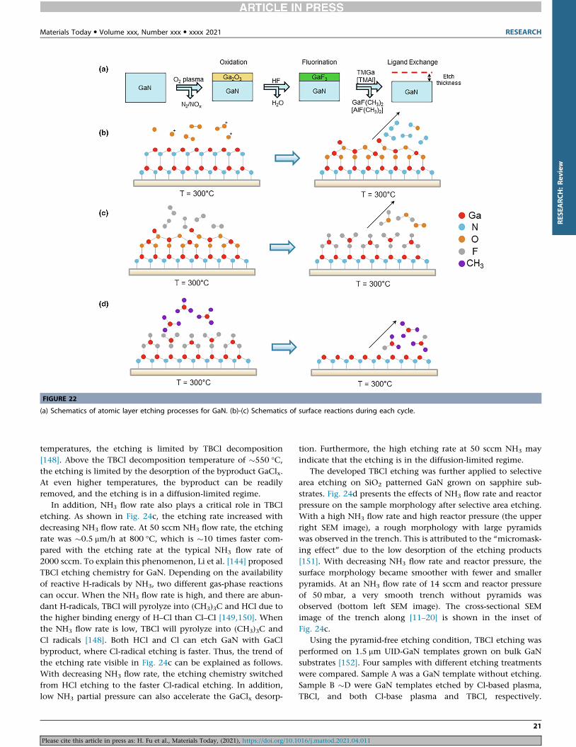
RES
EARCH:Rev
iew
FIGURE 22
(a) Schematics of atomic layer etching processes for GaN. (b)-(c) Schematics of surface reactions during each cycle.
Materials Today d Volume xxx, Number xxx d xxxx 2021 RESEARCH
temperatures, the etching is limited by TBCl decomposition[148]. Above the TBCl decomposition temperature of �550 �C,the etching is limited by the desorption of the byproduct GaClx.At even higher temperatures, the byproduct can be readilyremoved, and the etching is in a diffusion-limited regime.
In addition, NH3 flow rate also plays a critical role in TBCletching. As shown in Fig. 24c, the etching rate increased withdecreasing NH3 flow rate. At 50 sccm NH3 flow rate, the etchingrate was �0.5 mm/h at 800 �C, which is �10 times faster com-pared with the etching rate at the typical NH3 flow rate of2000 sccm. To explain this phenomenon, Li et al. [144] proposedTBCl etching chemistry for GaN. Depending on the availabilityof reactive H-radicals by NH3, two different gas-phase reactionscan occur. When the NH3 flow rate is high, and there are abun-dant H-radicals, TBCl will pyrolyze into (CH3)3C and HCl due tothe higher binding energy of H–Cl than Cl–Cl [149,150]. Whenthe NH3 flow rate is low, TBCl will pyrolyze into (CH3)3C andCl radicals [148]. Both HCl and Cl can etch GaN with GaClbyproduct, where Cl-radical etching is faster. Thus, the trend ofthe etching rate visible in Fig. 24c can be explained as follows.With decreasing NH3 flow rate, the etching chemistry switchedfrom HCl etching to the faster Cl-radical etching. In addition,low NH3 partial pressure can also accelerate the GaClx desorp-
Please cite this article in press as: H. Fu et al., Materials Today, (2021), https://doi.org/10.1
tion. Furthermore, the high etching rate at 50 sccm NH3 mayindicate that the etching is in the diffusion-limited regime.
The developed TBCl etching was further applied to selectivearea etching on SiO2 patterned GaN grown on sapphire sub-strates. Fig. 24d presents the effects of NH3 flow rate and reactorpressure on the sample morphology after selective area etching.With a high NH3 flow rate and high reactor pressure (the upperright SEM image), a rough morphology with large pyramidswas observed in the trench. This is attributed to the “micromask-ing effect” due to the low desorption of the etching products[151]. With decreasing NH3 flow rate and reactor pressure, thesurface morphology became smoother with fewer and smallerpyramids. At an NH3 flow rate of 14 sccm and reactor pressureof 50 mbar, a very smooth trench without pyramids wasobserved (bottom left SEM image). The cross-sectional SEMimage of the trench along [11–20] is shown in the inset ofFig. 24c.
Using the pyramid-free etching condition, TBCl etching wasperformed on 1.5 mm UID-GaN templates grown on bulk GaNsubstrates [152]. Four samples with different etching treatmentswere compared. Sample A was a GaN template without etching.Sample B �D were GaN templates etched by Cl-based plasma,TBCl, and both Cl-base plasma and TBCl, respectively.
21
016/j.mattod.2021.04.011

RESEA
RCH:R
eview
FIGURE 23
Thickness measurements during ALE of GaN using in situ ellipsometry for (a) 20 supercycles consisting of 3 alternating exposures of HF and TMG per O2
plasma, and (b) 10 supercycles consisting of 5 alternating exposures of HF and TMG per O2 plasma.
RESEARCH Materials Today d Volume xxx, Number xx d xxxx 2021
The photoluminescence (PL) in Fig. 24e showed strong near-band-edge emissions only from samples A, C, and D, indicatinga good surface. These samples either had no etching or TBCletching. Sample B with only Cl-based plasma etching had anobvious Cl peak from X-ray photoelectron spectroscopy (XPS),as shown in Fig. 24f. Sample D showed no Cl peak due to theTBCl etching after the plasma etching. These results suggest thatTBCl etching is able to remove the impurities and damageinduced by plasma etching and does not itself introduce damage.These results show that in situ TBCl etching can serve as an alter-native etching method but without plasma etching damage orhelp remove the plasma etching damage similar to the ALE. TBClin situ and selective area etching are very promising for selectivearea regrowth and doping in the fabrication of advanced GaNpower electronic devices. Due to the recent development of thesenovel etching technologies, future work is undergoing to demon-strate high-performance regrown devices using the ALE andTBCl-based in situ etching.
Regrown devicesDue to the immature status and the challenges for selective arearegrowth, very few regrown devices have so far been reported. Inthis section, two types of regrown devices are discussed, includ-
22
Please cite this article in press as: H. Fu et al., Materials Today, (2021), https://doi.org/10.1
ing GaN p-n diodes and VJFETs. Current regrown p-n diodesare still planar with decent performance. Low-leakage lateral p-n junctions are still under development. Nevertheless, the firstnormally-off VJFETs with regrown p-GaN gate were demon-strated, although leakage currents and breakdown voltages needfurther improvement.
p-n diodesRegrown p-n junctions are the cornerstone of selective areagrowth and doping. Although high performance lateral p-n junc-tions are still under development, several vertical regrown p-njunctions have been demonstrated. Hu et al. [91] reported a1.1-kV vertical GaN regrown p-n diode without ICP dry etchingwhere the p-GaN regrowth was completed using molecular beamepitaxy (MBE). The n-GaN drift layer was grown byMOCVDwitha thickness of 8 mm and a Si concentration of �2 � 1016 cm�3.The device had a specific on-resistance of 3.9 mO�cm2, a turn-on voltage of 3.9 V, an on/off ratio of �1011, and an ideality fac-tor of 2.5. Compared with the as-grown device with the samestructure, the regrown device showed high specific on-resistance and recombination currents due to the regrowth inter-face. The large reverse leakage current in the regrown device wasattributed to defect-assisted hopping conduction in the regrownp-GaN and/or at the regrowth interface.
016/j.mattod.2021.04.011
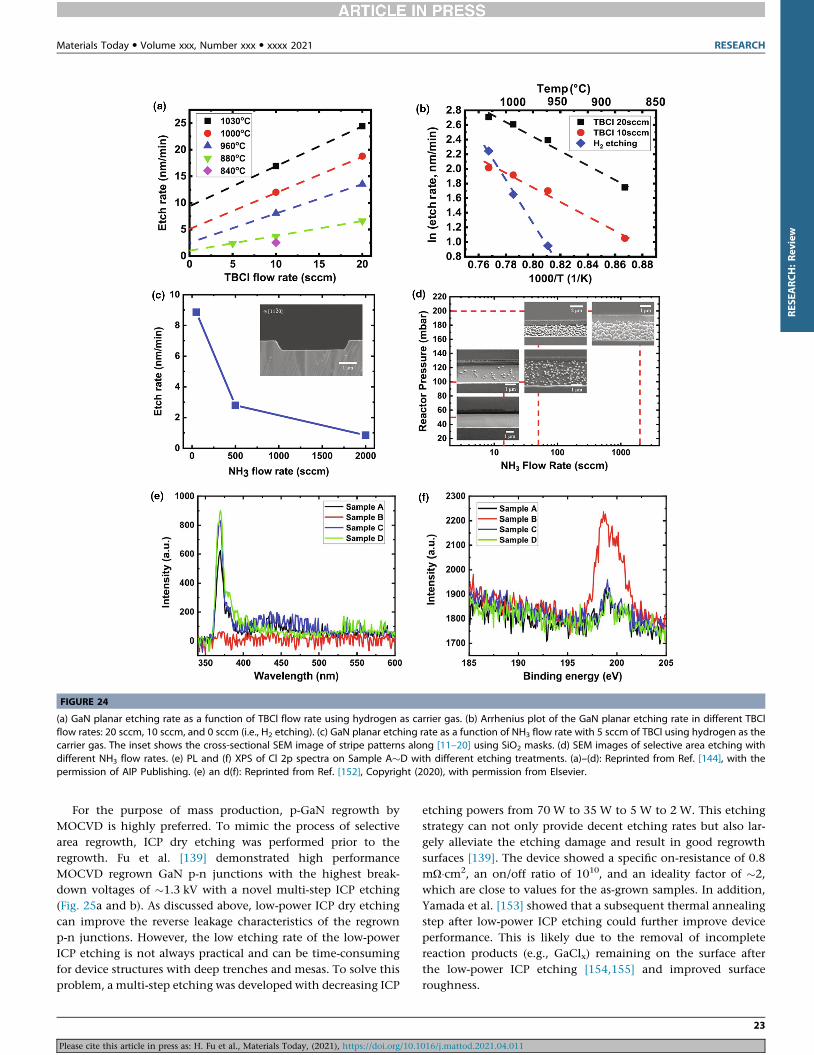
RES
EARCH:Rev
iew
FIGURE 24
(a) GaN planar etching rate as a function of TBCl flow rate using hydrogen as carrier gas. (b) Arrhenius plot of the GaN planar etching rate in different TBClflow rates: 20 sccm, 10 sccm, and 0 sccm (i.e., H2 etching). (c) GaN planar etching rate as a function of NH3 flow rate with 5 sccm of TBCl using hydrogen as thecarrier gas. The inset shows the cross-sectional SEM image of stripe patterns along [11–20] using SiO2 masks. (d) SEM images of selective area etching withdifferent NH3 flow rates. (e) PL and (f) XPS of Cl 2p spectra on Sample A�D with different etching treatments. (a)–(d): Reprinted from Ref. [144], with thepermission of AIP Publishing. (e) an d(f): Reprinted from Ref. [152], Copyright (2020), with permission from Elsevier.
Materials Today d Volume xxx, Number xxx d xxxx 2021 RESEARCH
For the purpose of mass production, p-GaN regrowth byMOCVD is highly preferred. To mimic the process of selectivearea regrowth, ICP dry etching was performed prior to theregrowth. Fu et al. [139] demonstrated high performanceMOCVD regrown GaN p-n junctions with the highest break-down voltages of �1.3 kV with a novel multi-step ICP etching(Fig. 25a and b). As discussed above, low-power ICP dry etchingcan improve the reverse leakage characteristics of the regrownp-n junctions. However, the low etching rate of the low-powerICP etching is not always practical and can be time-consumingfor device structures with deep trenches and mesas. To solve thisproblem, a multi-step etching was developed with decreasing ICP
Please cite this article in press as: H. Fu et al., Materials Today, (2021), https://doi.org/10.1
etching powers from 70W to 35 W to 5 W to 2W. This etchingstrategy can not only provide decent etching rates but also lar-gely alleviate the etching damage and result in good regrowthsurfaces [139]. The device showed a specific on-resistance of 0.8mO�cm2, an on/off ratio of 1010, and an ideality factor of �2,which are close to values for the as-grown samples. In addition,Yamada et al. [153] showed that a subsequent thermal annealingstep after low-power ICP etching could further improve deviceperformance. This is likely due to the removal of incompletereaction products (e.g., GaClx) remaining on the surface afterthe low-power ICP etching [154,155] and improved surfaceroughness.
23
016/j.mattod.2021.04.011

RESEA
RCH:R
eview
FIGURE 25
Reverse I–V characteristics of as-grown non-etched sample, sample with single-step etching, and sample with multi-step etching in (a) linear scale, and (b)semi-log scale. The devices were measured by Tektronix 370A curve tracer, and the leakage current measurements are limited by the relatively low currentresolution of the setup. (c) Benchmark plot of specific on-resistance versus breakdown voltages for reported as-grown and regrown GaN-on-GaN vertical p-ndiodes. All values of specific on-resistance are as-reported values and normalized by the area of p-contact. � [2019] IEEE. Reprinted with permission from Ref.[139].
RESEARCH Materials Today d Volume xxx, Number xx d xxxx 2021
For selective area regrowth in trenches, the regrowth inter-faces contain both c-plane and nonpolar m- or a-plane. Thesetwo types of crystal planes possess very different material proper-ties. For example, nonpolar planes have a larger tendency toincorporate impurities than c-plane. Aragon et al. [73] furtherrevealed that when the impurity concentration is moderate(<5 � 1017 cm�3), the forward and reverse characteristics of m-plane p-n diodes were not significantly degraded. When theimpurity concentration was high, different impurities showeddifferent impacts. High C levels did not increase the reverse leak-age current by much, while high Si and O levels led to very largereverse leakage currents. Monavarian et al. [69] showed aregrown nonpolar m-plane p-n junction without dry etching.The device showed a breakdown voltage of 540 V, a specificon-resistance of 1.7 mO�cm2, a turn-on voltage of �3 V, an on/off ratio of 109, and an ideality factor of 1.7. Fig. 25c presentsthe benchmark plot for the as-grown and regrown verticalGaN-on-GaN p-n diodes [139]. The Baliga’s figure of merit ofthe regrown p-n diodes by Fu et al. [139] was 2.0 GW/cm2, which
24
Please cite this article in press as: H. Fu et al., Materials Today, (2021), https://doi.org/10.1
is among the best performance in regrown devices and evencomparable to some of the as-grown devices. The performanceof GaN regrown p-n junctions is expected to approach the GaNmaterial limit with further improvements in the etching technol-ogy, surface treatment, and device fabrication.
Vertical junction field-effect transistorsGaN VJFETs were first proposed by Kizilyalli et al. [156], and Jiet al. [157] performed device simulations and optimization. Kot-zea et al. [158] showed GaN VJFETs on sapphire substrates with alow on/off ratio (less than 2) by selective area regrowth. How-ever, high performance GaN VJFETs have not been experimen-tally demonstrated on bulk GaN substrates. Based on the studyof selective area regrowth discussed above and a self-planarization process, Yang et al. [159] reported the first experi-mental demonstration of decent GaN VJFETs with a high on/off ratio of �100. The detailed fabrication process is shown inFig. 26. Each VJFET under test consisted of six fins with a lengthof 160 mm and a width of 1 mm. The current density was normal-
016/j.mattod.2021.04.011

FIGURE 27
(a) Cross-sectional SEM image of the first-generation VJFETs. (b) ID, IG–VG and (c) gm of the first-generation VJFETs at VD of 3 V. (d) Cross-sectional SEM image ofthe second-generation VJFETs. (e) ID, IG–VG and (f) gm of the second-generation VJFETs at VD of 10 V. � [2020] IEEE. Reprinted with permission from Ref. [159].
RES
EARCH:Rev
iew
FIGURE 26
Fabrication processes of the VJFETs. (a) Starting epilayers; (b) Cr and SiO2 hard masks; (c) e-beam lithography for fins; (d) Hard masks removal; (e) ICP etching;(f) Hard masks removal; (g) TMAH etching; (h) p-GaN regrowth; (i) Self-planarization using photoresist; (j) Top p-GaN removal; (k) Gate metal contactsdeposition; (l) Source and drain metal contacts deposition. � [2020] IEEE. Reprinted with permission from Ref. [159].
Materials Today d Volume xxx, Number xxx d xxxx 2021 RESEARCH
ized by the total active area of the fins. In the development ofnormally-off VJFETs, two sets of experiments were carried outto optimize the device growth and structures. In the first-generation VJFETs, no TMAH treatment was applied prior to p-
Please cite this article in press as: H. Fu et al., Materials Today, (2021), https://doi.org/10.1
GaN gate regrowth. Fig. 27a shows a cross-sectional SEM imageof the VJFETs. A slanted sidewall was clearly observed, leadingto a channel region with increasing width from top to bottom.In addition, an n+-GaN layer was employed as the source.
25
016/j.mattod.2021.04.011

RESEA
RCH:R
eview
RESEARCH Materials Today d Volume xxx, Number xx d xxxx 2021
Fig. 27b shows the transfer characteristics and gate leakage of theVJFETs. The device showed gate modulation. However, thedevice had a normally-on operation, possibly in part due to theslanted channel. In addition, the Ion/Ioff ratio was �6, and thegate leakage was relatively large. The transconductance gm exhib-ited two peaks (Fig. 27c), indicating the presence of interfacecharges.
Although the first-generation VJFETs have shown transistorcharacteristics, the relatively poor device performance may resultfrom a combination of factors such as interfacial defects andimpurities, etching damage, a slanted channel, and source-to-gate tunneling. To realize normally-off VJFETs with improvedperformance in the second-generation VJFETs, TMAH wet etch-ing, and UV-ozone and HF treatments were applied prior toregrowth to remove possible etching damage, and interfacialcharges and impurities. TMAH etching can also result in a morevertical sidewall aligned to m-plane (Fig. 27d). Furthermore, thesample did not have an n+-GaN layer as the source to preventforming Zener junctions between the source and the gate, whichmay give rise to a large gate leakage. Instead, the source regionwas treated with ICP etching to create donor-like surface defectsto facilitate contacts. Fig. 27e shows the transfer characteristicsand gate leakage of the second-generation VJFETs. A thresholdvoltage (Vth) of �1.3 V was obtained. At VGS = 3.4 V andVDS = 10 V, the drain current density reached �300 A/cm2. Fur-ther increase in VGS led to the forward bias of the gate-to-source junctions and the ramp-up of gate current. The Ion/Ioffwas improved significantly to �100. The gate leakage was alsoreduced compared with the first-generation VJFETs. Thetransconductance curves of the devices (Fig. 27f) showed a singlepeak with an excellent peak value of �200 S/cm2, which isamong the best values ever reported for vertical GaN VJFETs.The breakdown voltages of the devices were still relatively low(<100 V), which still need improvements. Recently, Liu et al.[160] demonstrated 1.2 kV-class Fin JFETs with avalanchecapability.
Conclusions and outlookThis paper reviews materials challenges and recent progress onselective area regrowth and doping for vertical GaN powerdevices. By investigating the effects of trench width and depthon regrowth, lateral and basal plane growth modes were identi-fied. Shallow trenches with an optimized width are optimal forselective area regrowth. Several materials characterization tech-niques were used to profile the dopant distributions at the sub-micron scale and to study the regrowth interface. It was foundthat there was nonuniform Mg distribution in a mesa or trenchstructure. The regrowth interface showed large amounts of impu-rities and charges, resulting in the formation of a p+-n+ tunnelingjunction. This may partly explain the large reverse leakage cur-rents in regrown p-n junctions. Three novel etching technologieswere employed to improve the regrowth interface. Low-powerICP dry etching significantly reduced the charge concentrationsat the regrowth interface and decreased the reverse leakage cur-rents. To reduce dry etching damage or replace ICP dry etching,PEC, ALE, and TBCl-based in situ and selective area etching havebeen developed, and relevant studies in selective area regrowth
26
Please cite this article in press as: H. Fu et al., Materials Today, (2021), https://doi.org/10.1
are ongoing. Based on the improved selective area regrowth,decent regrown p-n junctions and the first normally-off VJFETswere demonstrated. These results represent an important steptoward the realization of selective area regrowth and doping.
Despite this encouraging progress in selective area regrowthand doping for GaN, there are still some issues that remain tobe investigated and explored to facilitate the maturity of thetechnique. Firstly, most of the current materials characterizationsare based on planar etched samples. More work is needed on thecharacterizations of regrown structures in trenches (especiallytheir sidewalls), including impurity control, etching methods,post-etching treatments, and electronic structures. Electricalcharacterizations of the lateral p-n junctions are essential, includ-ing I–V and C–V. The current leakage through the sidewall mustbe suppressed for the lateral p-n junction to properly function incomplicated device structures. Secondly, most selective arearegrowth and doping studies are currently focused on the c-plane and nonpolar m-plane. However, ICP etching often resultsin a trench with a semipolar plane sidewall instead of anm-planesidewall. Regrowth dynamics and materials characterizations forsemipolar plane devices demand further investigation. Thirdly,although some etching techniques show promising results,how these novel etching technologies affect the performanceof regrown GaN devices still requires significant research effort.It is also important to investigate how to increase the etchingrate without creating more damage at the regrowth interface.Fourthly, there are currently still very few reports on regrownGaN devices, and the demonstrated devices usually have rela-tively simple structures. More complicated device structures suchas vertical GaN JBS/MPS rectifiers, JTE, and even insulated-gatebipolar transistors (IGBTs) should be studied. Finally, theregrowth interface in the regrown devices could become a relia-bility concern for mass production. Therefore, it is critical to eval-uate the stability of these regrown devices over an extended timeperiod under high temperature and high voltage stress. Compre-hensive failure analysis should be performed to identify the fail-ure modes and failure mechanisms, which can be used to assistthe device regrowth and design optimization.
Selective area regrowth and doping in vertical GaN powerdevices is a highly interdisciplinary area that requires collabora-tions from electrical engineers, materials, physicists, and che-mists. This comprehensive and timely review can serve as auseful reference for general readers and experts in the field, andshow the way to more opportunities for interdisciplinaryresearch and exciting advances in the development of verticalGaN power electronics and systems.
Declaration of Competing InterestThe authors declare that they have no known competing financial
interests or personal relationships that could have appeared to influ-ence the work reported in this paper.
AcknowledgmentThis work is supported by ARPA-E PNDIODES Program mon-
itored by Dr. Isik C. Kizilyalli.
References
[1] S. Chowdhury, U.K. Mishra, IEEE Trans. Electron Devices 60 (2013) 3060–3066.
016/j.mattod.2021.04.011

RES
EARCH:Rev
iew
Materials Today d Volume xxx, Number xxx d xxxx 2021 RESEARCH
[2] S. Chowdhury, et al., Semicond. Sci. Technol. 28 (2013) 074014.[3] H. Amano et al., J. Phys. D: Appl. Phys. 51 (2018) 163001[4] Y. Zhang, A. Dadgar, T. Palacios, J. Phys. D: Appl. Phys. 51 (2018) 273001.[5] J.Y. Tsao et al., Adv. Electron. Mater. 4 (2018) 1600501.[6] J. Wei et al., Jpn. J. Appl. Phys. 59 (2020) SG0801.[7] H. Fu, K. Fu, and Y. Zhao, “Vertical GaN-on-GaN power devices”, chapter in
“Wide bandgap semiconductors”, edited by Profs. S. J. Pearton and F. Ren, IOPScience, (2020).
[8] K.J. Chen et al., IEEE Trans. Electron Devices 64 (2017) 779–795.[9] R. Sun et al., IEEE Access 8 (2020) 15529–15542.[10] T. Ueda, Jpn. J. Appl. Phys. 58 (2019) SC0804.[11] T. Oka, Jpn. J. Appl. Phys. 58 (2019) SB0805.[12] I.C. Kizilyalli et al., IEEE Trans. Electron. Devices 62 (2015) 414–422.[13] Y. Cao, et al., Appl. Phys. Lett. 108 (2016) 062103.[14] H. Fu, et al., Appl. Phys. Lett. 111 (2017) 152102.[15] S. Han, S. Yang, K. Sheng, IEEE Electron. Device Lett. 40 (2019) 1040–1043.[16] S. Han, S. Yang, K. Sheng, IEEE Electron. Device Lett. 39 (2018) 572–575.[17] Y. Cao, et al., Appl. Phys. Lett. 108 (2016) 112101.[18] L. Sang et al., Appl. Phys. Lett. 111 (2017) 1221102.[19] B. Ren, et al., Appl. Phys. Express 10 (2017) 051001.[20] N. Tanaka, et al., Appl. Phys. Express 8 (2015) 071001.[21] Y. Saitoh, et al., Appl. Phys. Express 3 (2010) 081001.[22] H. Fu et al., IEEE Electron. Device Lett. 41 (2020) 127–130.[23] I.C. Kizilyalli, T. Prunty, O. Aktas, IEEE Electron. Device Lett. 36 (2015) 1073–
1075.[24] H. Fu et al., IEEE Electron Device Lett. 38 (2017) 763–766.[25] I.C. Kizilyalli et al., IEEE Trans. Electron Devices 60 (2013) 3067–3070.[26] H. Fu, et al., Appl. Phys. Express 11 (2018) 111003.[27] I.C. Kizilyalli et al., IEEE Electron. Device Lett. 35 (2014) 247–249.[28] J. Wang, et al., Appl. Phys. Lett. 113 (2018) 023502.[29] K. Nomoto et al., IEEE IEDM, (2015) 9.7.1-9.7.4.[30] J. Wang, et al., IEEE IEDM, (2017) 9.6.1-9.6.4.[31] Z. Hu et al., Appl. Phys. Lett. 107 (2015) 243501.[32] K. Nomoto et al., IEEE Electron Device Lett. 37 (2016) 161–164.[33] H. Fukushima S. Usami M. Ogura Y. Ando A. Tanaka M. Deki M. Kushimoto S.
Nitta Y. Honda H. Amano Jpn. J. Appl. Phys. 58 2019 SCCD25[34] H. Fukushima et al., Appl. Phys. Express 12 (2019) 026502.[35] T. Maeda, et al., IEEE IEDM, (2018) 30.1.1-30.1.4.[36] H. Fu et al., IEEE Electron Device Lett. 39 (2018) 1018–1021.[37] T. Maeda et al., IEEE Electron Device Lett. 40 (2019) 941–944.[38] H. Fu et al., Appl. Phys. Express 12 (2019) 051015.[39] S. Usami et al., Appl. Phys. Lett. 112 (2018) 182106.[40] B. Rackauskas et al., Appl. Phys. Lett. 112 (2018) 233501.[41] D. Ji, B. Ercan, S. Chowdhury, Appl. Phys. Lett. 115 (2019) 073503.[42] L. Cao, et al., Appl. Phys. Lett. 112 (2018) 262103.[43] Y. Zhang et al., IEEE Electron Device Lett. 38 (2017) 1097–1100.[44] Y. Zhang, et al., IEEE IEDM, (2016) 10.2.1-10.2.4.[45] Y. Zhang, et al., Appl. Phys. Lett. 110 (2017) 193506.[46] T. Hayashida et al., Appl. Phys. Express 10 (2017) 061003.[47] W. Li et al., IEEE Trans. Electron Devices 64 (2017) 1635–1641.[48] C. Gupta et al., IEEE Electron Device Lett. 38 (2017) 353–355.[49] D. Ji, et al., IEEE IEDM, (2017) 9.4.1-9.4.4.[50] D. Ji et al., IEEE Electron Device Lett. 39 (2018) 711–714.[51] T. Oka et al., Appl. Phys. Express 8 (2015).[52] T. Oka et al., Appl. Phys. Express 7 (2014).[53] R. Li et al., IEEE Electron Device Lett. 37 (2016) 1466–1469.[54] H. Nie et al., IEEE Electron Device Lett. 35 (2014) 939–941.[55] D. Shibata, et al., IEEE IEDM, (2016) 10.1.1-10.1.4.[56] D. Ji et al., IEEE Trans. Electron Devices 64 (2017) 805–808.[57] M. Sun et al., IEEE Electron Device Lett. 38 (2017) 509–512.[58] Y. Zhang, et al., IEEE IEDM, (2017) 9.2.1-9.2.4.[59] B.J. Baliga, Fundamentals of Power Semiconductor Devices, Springer-Verlag,
New York, 2008.[60] B.J. Baliga, Silicon Carbide Power Devices, World Scientific, Singapore, 2005.[61] W. Sung et al., IEEE Electron Device Lett. 32 (2011) 880–882.[62] A.V. Bolotnikov et al., IEEE Trans. Electron Devices 57 (2010) 1930–1935.[63] R. Ghandi et al., IEEE Trans. Electron Devices 58 (2011) 2665–2669.[64] A. Salemi et al., IEEE Electron Device Lett. 39 (2018) 63–66.[65] B.N. Feigelson et al., J. Cryst. Growth 350 (2012) 21–26.[66] J.D. Greenlee et al., ECS J. Solid State Sci. Technol. 4 (2015) P382–P386.[67] H. Sakurai et al., Appl. Phys. Lett. 115 (2019) 142104.[68] K. Fu et al., Appl. Phys. Lett. 113 (2018) 233502.[69] M. Monavarian et al., IEEE Electron Device Lett. 40 (2019) 387–390.
Please cite this article in press as: H. Fu et al., Materials Today, (2021), https://doi.org/10.1
[70] S.W. King et al., J. Appl. Phys. 84 (1998) 5248.[71] G. Koblmüller et al., J. Appl. Phys. 107 (2010) 043527.[72] A.L. Rosa, J. Neugebauer, Phys. Rev. B 73 (2006) 205314.[73] A. Aragon et al., Phys. Status Solidi A 217 (2020) 1900757.[74] M. Yang et al., J. Cryst. Growth 311 (2009) 2914–2918.[75] Z. Zheng et al., Phys. Status Solidi (a) 208 (2011) 951–954.[76] F. Yang et al., J. Mater. Sci. Mater. Electron. 26 (2015) 9753–9758.[77] S.R. Alugubelli et al., J. Appl. Phys. 126 (2019) 015704.[78] H. Liu, et al., Appl. Phys. Lett. 114 (2019) 082102.[79] P.-Y. Su et al., Appl. Phys. Lett. 117 (2020) 102110.[80] P.-Y. Su et al., J. Appl. Phys. 128 (2020) 055301.[81] H. Liu et al., J. Appl. Phys. 127 (2020) 195701.[82] K. Hiramatsu et al., J. Cryst. Growth 221 (2000) 316.[83] J. Wang et al., Semicond. Sci. Technol. 35 (2020) 125026.[84] S. Nakamura et al., Jpn. J. Appl. Phys. 31 (2020) 1258.[85] S.M. Myers et al., J. Appl. Phys. 89 (2001) 3195.[86] Y. Kuwano et al., Jpn. J. Appl. Phys. 52 (2013) 08JK12.[87] W. Li et al., Appl. Phys. Lett. 113 (2018).[88] W. Li et al., IEEE Trans. Electron Devices 65 (2018) 2558–2564.[89] W. Li et al., Proc. 75th Annu. Device Res. Conf. (DRC) (2017).[90] W. S. Li, et al., Jpn. J. Appl. Phys., Part 1 58 (2019) SCCD15.[91] Z. Hu et al., IEEE Electron Device Lett. 38 (2017) 1071–1074.[92] S. Guha et al., Appl. Phys. Lett. 75 (1999) 463.[93] H. Sekiguchi et al., Appl. Phys. Express 1 (2008) 124002.[94] A. Bengoechea-Encabo et al., J. Cryst. Growth 325 (2011) 89.[95] R. Yeluri et al., Appl. Phys. Lett. 106 (2015) 183502.[96] K. Grabianska et al., Electronics 9 (2020) 1342.[97] B. Raghothamachar et al., J. Cryst. Growth 544 (2020) 125709.[98] Y. Liu et al., J. Cryst. Growth 551 (2020) 125903.[99] M. Lee et al., CrystEngComm. 19 (2017) 2036.[100] P. Peri, et al., J. Vac. Sci. Technol. A 38 (2020) 063402.[101] S.C. Cruz et al., J. Cryst. Growth 311 (2009) 3817–3823.[102] A. Chakraborty et al., J. Appl. Phys. 96 (2004) 4494.[103] J. Wang et al., Phys. Status Solidi A 211 (2014) 2645–2649.[104] F. Shahedipour, B.W. Wessels, Appl. Phys. Lett. 76 (2000) 3011.[105] H. Amano et al., J. Electrochem. Soc. 137 (1990) 1639.[106] U. Kaufmann et al., Appl. Phys. Lett. 72 (1998) 1326.[107] J. Cazaux, J. Electron Microsc. 61 (2012) 261.[108] J.R. Dennison, A. Sim, C.D. Thomson, IEEE Trans. Plasma Sci. 34 (2006) 2204–
2218.[109] H. Seiler, J. Appl. Phys. 54 (1983) R1.[110] J. Goldstein, Scanning Electron Microscopy and X-ray Microanalysis, 4th ed.,
Springer Science, New York, 2017, p. 88.[111] D.C. Joy, Scanning 11 (1989) 1.[112] L. Reimer, C. Tollkamp, Scanning 3 (1980) 35.[113] J.P. Long, V.M. Bermudez, Phys. Rev. B 66 (2002) 121308.[114] K.M. Tracy et al., J. Appl. Phys. 94 (2003) 3163.[115] D.D. Perovic et al., Ultramicroscopy 58 (1995) 104.[116] I. Volotsenko, et al., J. Appl. Phys. 107 (2010) 014510.[117] A. Shih et al., J. Appl. Phys. 82 (1997) 1860.[118] G.F. Dionne, J. Appl. Phys. 46 (1975) 3347.[119] A.S. Chang et al., A.C.S. Appl. Electron. Mater. 3 (2021) 704–710.[120] P. Peri et al., J. Electron. Mater. 50 (2021) 2637–2642.[121] H. Fu et al., IEEE Electron Device Lett. 38 (2017) 1286–1289.[122] J. Montes et al., IEEE Trans. Nucl. Sci. 66 (2019) 91–96.[123] H. Fu et al., IEEE Trans. Electron Devices 65 (2018) 3507–3513.[124] T. Yang, et al., J. Semicond. 40 (2019) 012801.[125] I. Stricklin et al., Proc. SPIE 10754 (2018) 1075402.[126] K. Fu et al., IEEE Electron Device Lett. 40 (2019) 375–378.[127] M.R. McCartney, D.J. Smith, Annu. Rev. Mater. Res. 37 (2007) 729.[128] S. R. Alugubelli, et al., Appl. Phys. Lett. 115 (2019) 201602.[129] H. Katayama-Yoshida et al., J. Phys.: Condens. Matter 13 (2001) 8901.[130] Y. Akatsuka, et al., Appl. Phys. Express 12 (2019) 025502.[131] E.T. Yu et al., J. Appl. Phys. 79 (1996) 2115.[132] P.A. Rosenthal et al., J. Appl. Phys. 87 (2000) 1937.[133] P.A. Rosenthal, Y. Taur, E.T. Yu, Appl. Phys. Lett. 81 (2002) 3993.[134] J. Sumner, et al., J. Appl. Phys. 106 (2009) 104503.[135] J. Sumner et al., Phys. Status Solidi B 245 (2008) 896–898.[136] Y.J. Han et al., Jpn. J. Appl. Phys. 42 (2003) 6409.[137] S. Tripathy et al., J. Vac. Sci. Technol. A 19 (2001) 2522.[138] T. Narita et al., Phys. Status Solidi A 208 (2011) 1541.[139] K. Fu et al., IEEE Electron Device Lett. 40 (2019) 1728–1731.[140] G. W. Pickrell, et al., J. Appl. Phys. 126 (2019) 145703.
27
016/j.mattod.2021.04.011

RESEA
RCH:R
eview
RESEARCH Materials Today d Volume xxx, Number xx d xxxx 2021
[141] A. Aragon, et al., J. Appl. Phys. 128 (2020) 185703.[142] Y. Lee, J.W. Dumont, S.M. George, Chem. Mater. 28 (2016) 2994–3003.[143] Y. Lee, S.M. George, Chem. Mater. 29 (2017) 8202–8210.[144] B. Li et al., Appl. Phys. Lett. 115 (2019) 162101.[145] T.H. Myers et al., J. Cryst. Growth 246 (2002) 244–251.[146] D. Fahle et al., J. Cryst. Growth 393 (2014) 89–92.[147] J. Han et al., Appl. Phys. Lett. 71 (1997) 3114.[148] M. Kondow, B. Shi, C.W. Tu, Jpn. J. Appl. Phys. Part 2 (38) (1999) L617.[149] Q. An et al., J. Phys. Chem. C 119 (2015) 4095.[150] D.R. Lide, CRC Handbook of Chemistry and Physics, CRC Press (1999–2000).
28
Please cite this article in press as: H. Fu et al., Materials Today, (2021), https://doi.org/10.1
[151] D. Franke et al., J. Cryst. Growth 248 (2003) 421–425.[152] B. Li et al., J. Cryst. Growth 534 (2020) 125492.[153] S. Yamada et al., Appl. Phys. Express 13 (2020) 016505.[154] S.J. Pearton et al., J. Appl. Phys. 86 (1999) 1.[155] F.A. Khan et al., J. Vac. Sci. Technol. B 19 (2001) 2926.[156] I.C. Kizilyalli, O. Aktas, Semicond. Sci. Technol. 30 (2015).[157] D. Ji, S. Chowdhury, IEEE Trans. Electron Devices 62 (2015) 2571–2578.[158] S. Kotzea et al., IEEE Trans. Electron Devices 65 (2018) 5329–5336.[159] C. Yang et al., IEEE Trans. Electron Devices 67 (2020) 3972–3977.[160] J. Liu et al., IEEE Trans. Electron Devices 68 (2021) 2025–2032.
016/j.mattod.2021.04.011