mixer dissertation P-II
46
Linearity Optimization of RF Analog Down Conversion Mixer Designed for 2.4GHz Applications Presented by: Mr. Shiven Pandya P.G Student, MEFGI, Rajkot. Enroll. No. 130570742011 Guided by : Mr. Amit Kumar Asst. Professor, MEFGI, Rajkot. 1
-
Upload
shiven-pandya -
Category
Documents
-
view
1.157 -
download
0
Transcript of mixer dissertation P-II
Linearity Optimization of RF Analog
Down Conversion Mixer Designed
for 2.4GHz Applications
Presented by:
Mr. Shiven Pandya
P.G Student, MEFGI, Rajkot.
Enroll. No. 130570742011
Guided by :
Mr. Amit Kumar
Asst. Professor, MEFGI, Rajkot.
1

Outlines
• Introduction
• Optimization Techniques
• Roadmap to Optimization
• Layout
• Parameters Comparison
• Conclusions
2

What is Mixer?
• Non-Linear Analog device
• Frequency Translator
4
Local
Osc.
LNA Down conversion Mixer
RF
LO
IF
Antenna
Fig.1: RF Front End / Role of mixer in generic receiver
If the inputs are sinusoids,
the ideal mixer output is the sum and difference frequencies given by
Vo = [A1cos(𝜔1𝑡)] [A2cos(𝜔2𝑡)] = 𝐴1𝐴22[cos 𝜔1− 𝜔2 𝑡 + [cos 𝜔1+ 𝜔2 𝑡]

Mixer Output Components
• Nonlinear relation between Input and Output is given by :
Vout = a0 + a1Vin + a2Vin2 + a3Vin
3 + Higher order terms
5
a0 --- DC Biased
a1Vin --- Linear Term (Amplifiers)
a2Vin2 --- Detectors / Mixers
a3Vin3 --- Undesired Spurious Signals (Noise)
Table showing harmonics of fout
Order of
Harmonics
Components of fout
1st order fRF , fLO
2nd order 2fRF , 2fLO
fLO - fRF , fLO + fRF
3rd order 3fRF , 3fLO
2fLO - fRF , 2fLO + fRF ,
fLO - 2fRF , fLO + 2fRF
Pow
er
Frequency
fIF = | fLO – fRF |
IF
RF
LO
Pow
er
Fig.2: Intermediate Frequency at output FFT

3rd Order Input Intercept Point
(Linearity)
• Input / Output relation of the transconductor is
Iout = a0 + a1Vin + a2Vin2 + a3Vin
3 + Higher order terms
6
Two Tones at Input : f1 and f2
Table showing harmonics
Order of Harmonics Components
1st order f1 , f2
2nd order 2f1 , 2f2
f1- f2 , f1 + f2
3rd order 3f1 , 3f2
2f1 – f2 , 2f1 + f2 ,
f1 - 2f2 , f1 + 2f2
Vin
Iout
Fig.3: RF Port
Pow
er
Fundamentals
Frequency
3rd order products
5th order products
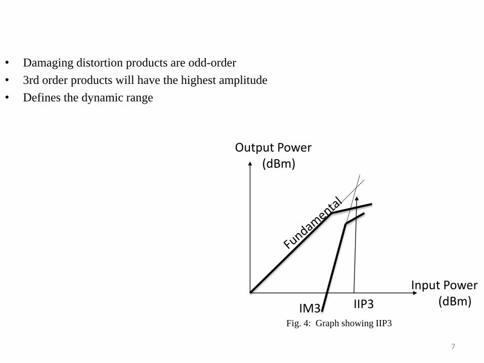
7
• Damaging distortion products are odd-order
• 3rd order products will have the highest amplitude
• Defines the dynamic range
Fig. 4: Graph showing IIP3
Input Power(dBm)
Output Power(dBm)
IIP3IM3

Linearity
• Compound FET’s [6]
• Source Degeneration Resistors[10]
• Subharmonics Pumped Technique[11]
Conversion Gain
• Current Bleeding [4]
• Shunt Peaking Tuning[10]
• Current Injection [7]
9
Parameter
Optimization
Technique
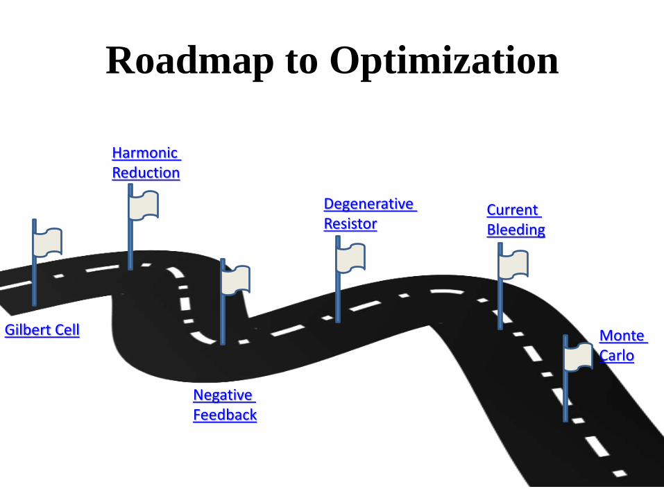
Roadmap to Optimization
10
Gilbert Cell
Harmonic Reduction
Negative Feedback
Degenerative Resistor
Current Bleeding
Monte Carlo
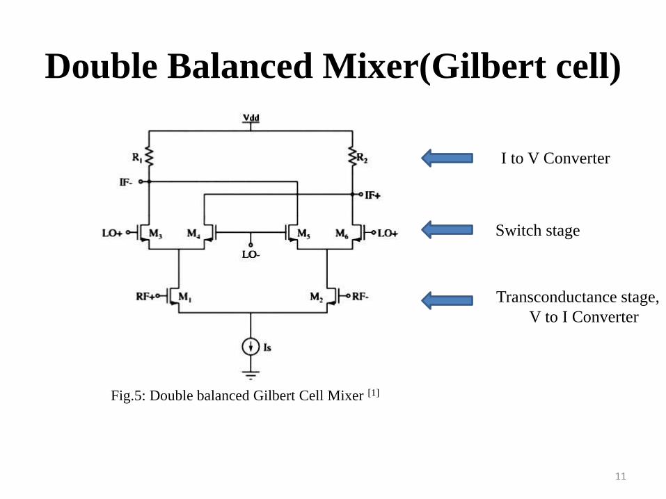
Double Balanced Mixer(Gilbert cell)
11
Transconductance stage,
V to I Converter
Switch stage
I to V Converter
Fig.5: Double balanced Gilbert Cell Mixer [1]

12
Output will have: Even harmonics
Fourier series of LO signal
S(t) = 𝑎0
2+ 𝑛=1
∞ 𝑎𝑛 cos(𝑛𝜔𝐿𝑂𝑡 + 𝑏𝑛 sin(𝑛𝜔𝐿𝑂𝑡)
Harmonics as𝑎𝑛 ≠ 0Frequency
Gain
Fig.6: FFT of output signal

Harmonic Reduction
• LO is switching signal
• Operate in Cuttoff & Saturation Region
13
No perfect square wave ??
- Shifting signal upward and downward
- Change in duty cycle
+1
0
Sgn (sinωLO)
Fig.7: sin 𝜔𝐿𝑂𝑡 & sgn(sin 𝜔𝐿𝑂𝑡 )
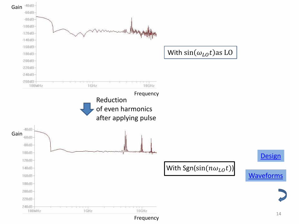
14
Reduction of even harmonics after applying pulse
Design
Waveforms
Frequency
Frequency
Gain
Gain
With sin 𝜔𝐿𝑂𝑡 as LO
With Sgn(sin(𝑛𝜔𝐿𝑂𝑡))

15
Negative Feedback[1]
Causes of distortion due to intermodulation products
Vin
Iout
Linear Input
Nonlinear Output
Amplitude Distortions
Makes output drive in Saturation or Cuttoff
Frequency Distortions
Frequency dependent effects of reactive components
F(Hz)
GainPoor HF gain
F(Hz)
GainToo much HF gain
Fig.8: Amplitude Distortion
Fig.9: Frequency vs Gain

16
Negative Feedback
• Subtracts a fraction of its output from its input
• Higher Linearity (Reduces Distortions)
• Increases Bandwidth
R
INIF
Fig.10 Negative feedback[1]
Closed loop Gain Afb = AOL
1+ 𝛽AOL
Negative feedback Keeps gain at a constant level

Degenerative Resistors
R R
RF+ RF-
17
Principle of Linearization Reduce the dependence of the gain
of the circuit upon input level
𝐺𝑚 =𝑔𝑚
1 + 𝑔𝑚𝑅For large 𝑔𝑚𝑅 approaches
1
𝑅
Waveforms
Design
Fig.11 : R as Degenerative resistors[11]

18
Current Bleeding Technique
Fig.12 : Current bleeding circuit[5]
LO+ LO-
VDD
V
Driver Current
Pmos is used as a bleeding current source
Higher IP3 than the conventional mixer
Conversion Gain = 4
𝜋𝑔𝑚𝑅𝐿𝑜𝑎𝑑
IIP3 = 32 𝐼𝐷
3𝛽𝑛
For a Gilbert Cell Mixer :

19
Computational algorithms Repeated random sampling
to obtain numerical results
Monte Carlo Simulation
Component Values
WM1-M4, WM9-10 6µm
WM5,M6 0.59µm
WM7,M8 0.61µm
Values after Monte Carlo Simulation
Fig.13 : Gaussian Distribution

Switch
1
Switch
2
Switch
3
Switch
4
Current
Source
Current
Bleeding
Current
Bleeding
Negative
Feedback
Negative
Feedback
Driver/RF Stage
IF+ IF-
RF+ RF-
VDD
Load Load
LO+ LO+
LO-
21
Proposed Block Diagram
Proposed Design
22
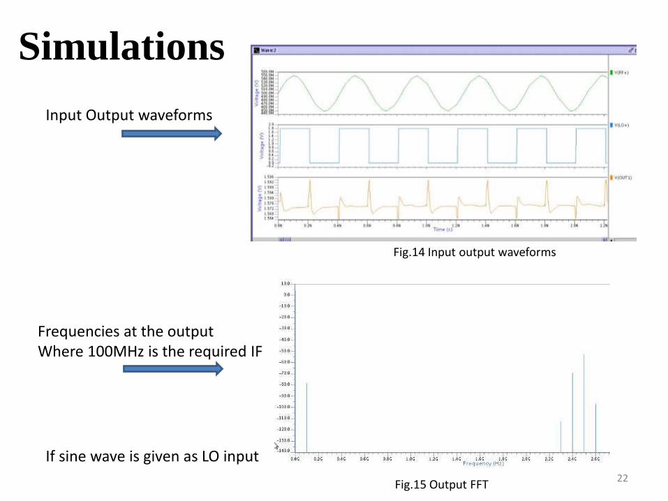
Input Output waveforms
Frequencies at the outputWhere 100MHz is the required IF
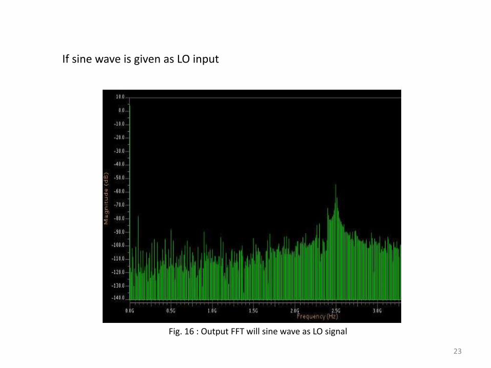
If sine wave is given as LO input
Fig.15 Output FFT
Fig.14 Input output waveforms
Simulations
23
Fig. 16 : Output FFT will sine wave as LO signal
If sine wave is given as LO input

24
Fig.18 : IIP3 point
Fig.17 : Intermodulation products
Fig.19 : 1dB Compression point
2-Tone set up:Fund. Tone 1 : 2.40Fund. Tone 2 : 2.41
25
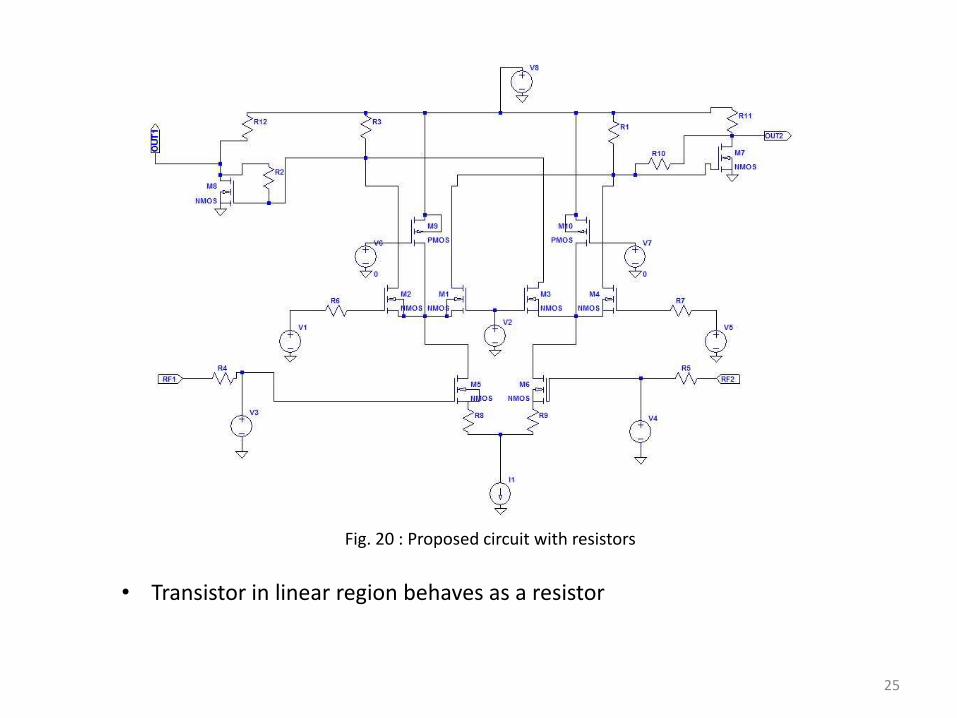
• Transistor in linear region behaves as a resistor
Fig. 20 : Proposed circuit with resistors

26
Component W VGATE
Current source
1.5µ 0.5V
50Ω 90µ 0.5V
113Ω 100µ 2.2V
255Ω 75µ 2.2V
1000Ω 20µ 2.2V
Fig. 21 : Transistors replacing resistors

27
Layout
Fig. 22 : Layout of proposed work
28
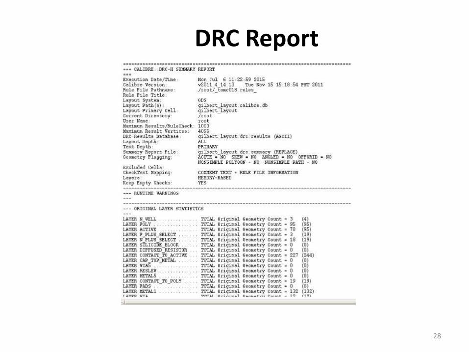
DRC Report

Prelayout in ADS
29Fig. 23 : Schematic in ADS
Fig. 24 : Symbol of the circuit

30
Converting the 11 pin IC to a 2 pin setup
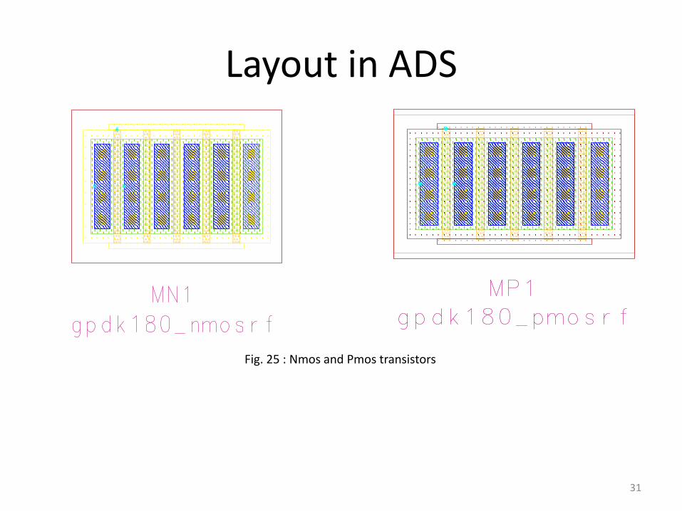
Layout in ADS
31
Fig. 25 : Nmos and Pmos transistors
33
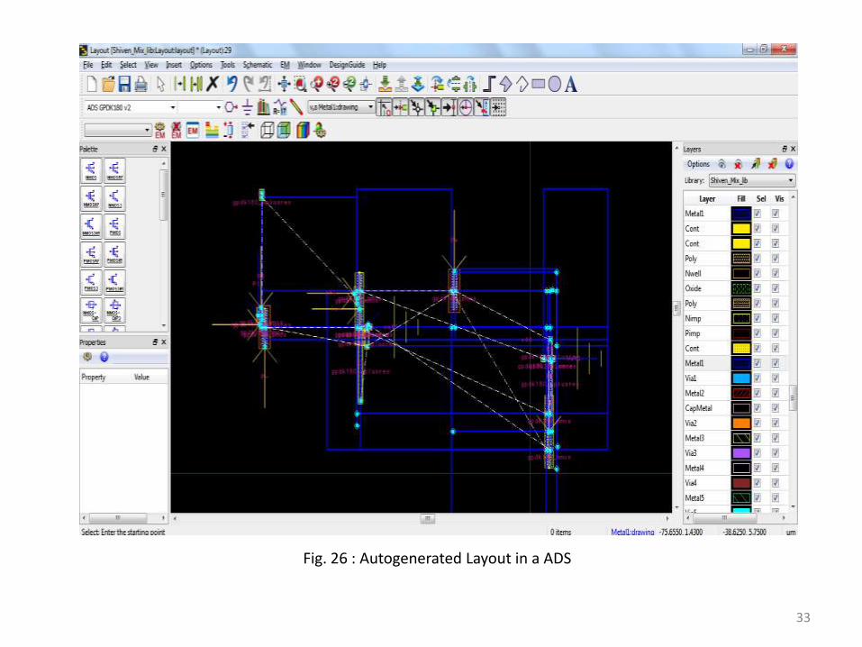
Fig. 26 : Autogenerated Layout in a ADS

35
Fig. 28 : Final Layout in ADS
Resistors are replaced by GPDK pwell resistors
36
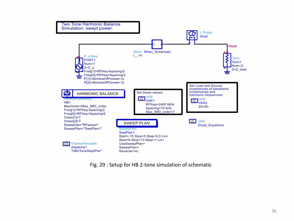
Fig. 29 : Setup for HB 2-tone simulation of schematic

37
Fig. 30 : Setup for HB 2-tone simulation of layout

Comparing IIP3 Point
39
Prelayout
IIP3 = 10dBm
Postlayout
IIP3 = -5dBm
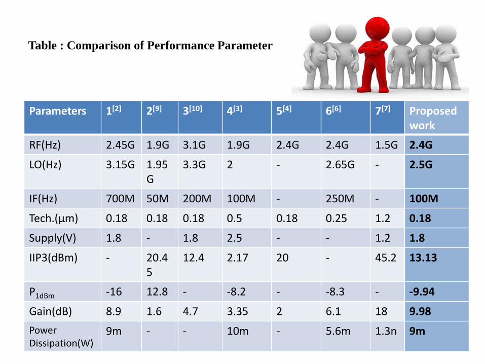
Table : Comparison of Performance Parameter
42
Parameters 1[2] 2[9] 3[10] 4[3] 5[4] 6[6] 7[7] Proposed work
RF(Hz) 2.45G 1.9G 3.1G 1.9G 2.4G 2.4G 1.5G 2.4G
LO(Hz) 3.15G 1.95G
3.3G 2 - 2.65G - 2.5G
IF(Hz) 700M 50M 200M 100M - 250M - 100M
Tech.(µm) 0.18 0.18 0.18 0.5 0.18 0.25 1.2 0.18
Supply(V) 1.8 - 1.8 2.5 - - 1.2 1.8
IIP3(dBm) - 20.45
12.4 2.17 20 - 45.2 13.13
P1dBm -16 12.8 - -8.2 - -8.3 - -9.94
Gain(dB) 8.9 1.6 4.7 3.35 2 6.1 18 9.98
PowerDissipation(W)
9m - - 10m - 5.6m 1.3n 9m

Conclusions• Design Optimized for a Down Conversion Mixer for ISM Band 2.4GHz
application with 0.18 µm CMOS Technology
• Incorporating the degenerative resistors, current bleeding technique and
negative feedback in the standard gilbert cell mixer
• Monte Carlo optimization algorithm gives 3rd order Input Intercept point
(IIP3) at 13.13dBm
• Tools used : Mentor Graphics Tool Suite, Hspice (Synopsys) and ADS.
46

References
1. B. Razavi, RF Microelectronics, New Jersey: Prentice-Hall, 1998.
2. Pokle, “VLSI design of ISM band RF down conversion mixer”, IEEE Thirdinternational conference on emerging trends in engineering and technology, 2010.
3. Kilicaslan, Ismail, “A 1.9 GHz CMOS RF Down Conversion Mixer”, IEEEProceedings of the 40th Midwest Symposium on Circuits and Systems, 1997.
4. Tsai, “Design of 40-80 GHz Low power and High Speed CMOS Down ConversionRing Mixer for Multistand MMW Radio Applications”, IEEE Transactions ofMicrowave Theory and Techniques, Vol.60,No. 3,March 2012.
5. Lee, “ Current-reuse bleeding Mixer”, IEEE Electronics Letters , Vol.36 No.8, April2000.
6. Siddiqi,“2.4 GHz RF Down-conversion Mixers in Standard Cmos Technology”, IEEEJournal of Solid State Circuits, vol. 36, NO. 12, 2004.
47
7. Wei, “A 1.5V High Linearity Down-Conversion Mixer for WiMAX Application”, IEEE
2nd International Conference on Mechanical and Electronics Engineering, vol. 2 , 2010.
8. MacEachern,Manku “A Charge Injection Method for Gilbert Cell Biasing”, IEEE
Canadian Conference on Electrical and Computer Engineering, vol. 1, 1998.
9. Islam,Huq “ High Performance CMOS Converter Design in TSMC 0.18µm Process”,
IEEE Southeast Conference, 2005.
10. Pandram “A Low Power down Conversion CMOS Gilbert Mixer for WirelessCommunications”, Int. Journal of Engineering Research and Applications, Vol. 4, Issue7(Version 1), July 2014.
11. Lu Hung, “A 0.18µm CMOS High Linearity Flat Conversion Gain Down-conversion
Mixer for UWB Receiver”, IEEE Asia Pacific Conference on Circuits and Systems , 2008.
48

Thank You . .
49

50
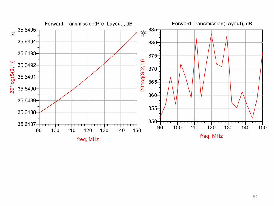
51
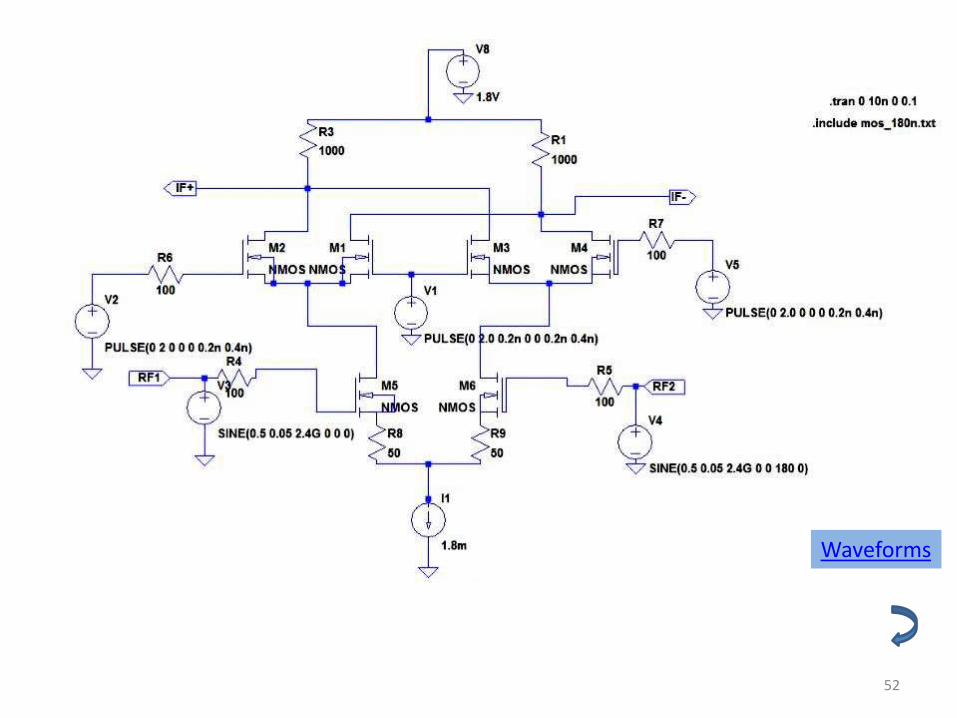
52
Waveforms

53
RF = 2.4 GHz at 0.5 VLO = 2.5 GHz at 1.8VConversion Gain: 4.13 dB

54
Waveforms

55
RF = 2.4 GHz at 0.5 VLO = 2.5 GHz at 1.8VConversion Gain: 9.93 dB

56

57
V4 RF2 0 0.5V5 N007 0 PULSE(0 2.0 0 0 0 0.2ns 0.4ns)M7 OUT2 N003 0 N004 NMOS l=180n w=xM8 OUT1 N002 0 N005 NMOS l=180n w=xR2 N003 OUT2 aR10 OUT1 N002 aR11 N001 OUT2 255R12 N001 OUT1 255
V3 N015 N016 dc=0 z0=50 power=1 $50 Ohm src
+ HB Pin:W 0 1 1 $ tone 1+ HB Pin:W 0 1 2 $ tone 2
.HB tones=2400MEG,2410MEG nharms=3 3 intmodmax=7 Sweep monte = 100 + SWEEP Pin:dBm -50.0 0 2.0
*.print HB P(R12) P(R12)[1,0] P(R12)[2,-1]*.probe HB P(R12) P(R12)[1,0] P(R12)[2,-1]
.OPTION LIMPROBE = 10000