
MIL-STD-1553 Transceiver and Transformer Residual Voltage ... · This section describes...
31
9502011-001 1 Cobham Semiconductor Solutions Version 2.0.0 Cobham.com/HiRel Transformer Recommendation for Optimal MIL-STD-1553 Residual Voltage when Interfacing to Cobham Transceivers Table 1: Cross Reference of Applicable Products PRODUCT NAME MANUFACTURER PART NUMBER SMD # DEVICE TYPE INTERNAL PIC NUMBER UT63M147 Bus Transceiver UT63M147 5962-93226 03, 04 JB01 JB03 UT63M143 Bus Transceiver UT63M143 5962-07242 01, 02 JB04 JB05 UT63M1X5C Bus Transceiver UT63M1X5C N/A N/A BA02 SμMMIT DXE UT69151 DXE 5962-94663 08, 11 MM016 MM023 MM025 MM027 SμMMIT XTE UT69151 XTE 5962-94758 08 MM019 SμMMIT RTE UT69151 RTE 5962-98587 01 MM022 1.0 Overview The objective of this product advisory is to inform MIL-STD-1553 circuit designers of lessons learned during a residual voltage investigation and to offer some transformer selection recommendations to minimize residual voltage. 2.0 Background Cobham recently worked with a customer who observed unexpectedly high residual voltage amplitude and a high degree of residual voltage variance across a small sample of MIL-STD-1553 terminals during system level testing. A bus monitor flagged the anomaly while the Terminal-Under-Test maintained error free communication with the test side bus controller. Cobham worked extensively with its customer to evaluate all aspects of their circuit and system design and test network, which included evaluating a test-side bus controller and MIL-STD-1553 bus monitor, to understand the cause of the variance. The investigation method was to isolate, swap, compare, and contrast every aspect of the system, circuit design, manufacturing and component handling/accountability systems. Disqualifying one variable at a time, the investigation team reduced the anomalistic problem area to the interaction between Cobham’s transceiver and the transformer. MIL-STD-1553B requires that all MIL-STD-1553 terminals meet the output symmetry requirements as defined in section 4.5.2.1.1.4 for transformer-coupled (4.5.2.2.1.4 for direct-coupled) terminals. This requirement ensures that a terminal completing a transmission does not leave a residual voltage on the bus that interferes with the sync pulse of a subsequent message. If a residual voltage with a high enough amplitude is present on the bus while another terminal begins transmission, the residual voltage can affect the incoming message such that the intended target fails to properly decode the message. Standard Product MIL-STD-1553 Transceiver and Transformer Residual Voltage Compatibility Product Advisory Cobham.com/HiRel December 11, 2015 The most important thing we build is trust
Transcript of MIL-STD-1553 Transceiver and Transformer Residual Voltage ... · This section describes...

9502011-001 1 Cobham Semiconductor Solutions Version 2.0.0 Cobham.com/HiRel
Transformer Recommendation for Optimal MIL-STD-1553 Residual Voltage when Interfacing to Cobham Transceivers
Table 1: Cross Reference of Applicable Products
PRODUCT NAME MANUFACTURER PART NUMBER SMD # DEVICE
TYPE INTERNAL PIC
NUMBER
UT63M147 Bus Transceiver UT63M147 5962-93226 03, 04 JB01 JB03
UT63M143 Bus Transceiver UT63M143 5962-07242 01, 02 JB04 JB05
UT63M1X5C Bus Transceiver UT63M1X5C N/A N/A BA02
SµMMIT DXE UT69151 DXE 5962-94663 08, 11
MM016 MM023 MM025 MM027
SµMMIT XTE UT69151 XTE 5962-94758 08 MM019 SµMMIT RTE UT69151 RTE 5962-98587 01 MM022
1.0 Overview
The objective of this product advisory is to inform MIL-STD-1553 circuit designers of lessons learned during a residual voltage investigation and to offer some transformer selection recommendations to minimize residual voltage.
2.0 Background
Cobham recently worked with a customer who observed unexpectedly high residual voltage amplitude and a high degree of residual voltage variance across a small sample of MIL-STD-1553 terminals during system level testing. A bus monitor flagged the anomaly while the Terminal-Under-Test maintained error free communication with the test side bus controller. Cobham worked extensively with its customer to evaluate all aspects of their circuit and system design and test network, which included evaluating a test-side bus controller and MIL-STD-1553 bus monitor, to understand the cause of the variance.
The investigation method was to isolate, swap, compare, and contrast every aspect of the system, circuit design, manufacturing and component handling/accountability systems. Disqualifying one variable at a time, the investigation team reduced the anomalistic problem area to the interaction between Cobham’s transceiver and the transformer.
MIL-STD-1553B requires that all MIL-STD-1553 terminals meet the output symmetry requirements as defined in section 4.5.2.1.1.4 for transformer-coupled (4.5.2.2.1.4 for direct-coupled) terminals. This requirement ensures that a terminal completing a transmission does not leave a residual voltage on the bus that interferes with the sync pulse of a subsequent message. If a residual voltage with a high enough amplitude is present on the bus while another terminal begins transmission, the residual voltage can affect the incoming message such that the intended target fails to properly decode the message.
Standard Product
MIL-STD-1553 Transceiver and Transformer Residual Voltage Compatibility Product Advisory Cobham.com/HiRel December 11, 2015
The most important thing we build is trust

9502011-001 2 Cobham Semiconductor Solutions Version 2.0.0 Cobham.com/HiRel
Output symmetry is strongly dependent upon electrical imbalances in the closed-loop system created by the digital MIL-STD-1553 protocol device, the differential transceiver, and a center-tapped isolation transformer. All three devices work cooperatively to drive Manchester-II bi-phase encoded signals onto the MIL-STD-1553 bus. Manchester-II bi-phase signaling encodes clock and data onto a single wire pair while maintaining a zero DC bias on the physical interconnect. In an ideal MIL-STD-1553 bus, the zero DC voltage bias occurs because positive energy in the system exactly matches the negative energy.
However, the reality is that non-idealities in the components and their connection to one another create an imbalance in the system. Some of this imbalance is inherent to the MIL-STD-1553 terminal components themselves, while others are dependent upon the terminal designer’s decoupling, layout, and assembly decisions. This product advisory focuses on the former. Although the circuit designer cannot substantively affect the actual interaction between the specific transformer and transceiver combination, having awareness of the device characteristics related to output symmetry and using these insights to select and screen components is an effective strategy to maximize energy transfer in the system and assuring minimal residual voltage on the MIL-STD-1553 serial bus.
2.1 Definition of Residual Voltage
To determine output symmetry, measure the waveform tail-off time (TT) after the end of each valid transmitted message as shown in Figure 1. The residual voltage (VR) on the bus is the resulting measure of output symmetry. The pass criteria for residual voltage is ±250mV peak, line-to-line, for transformer-coupled terminals and ±90mV peak, line-to-line, for direct-coupled terminals. Measure VR at Point A (see Figure 2) in a MIL-STD-1553 system 2.5µs after the mid-bit zero crossing of the parity bit.
Figure 1. MIL-STD-1553 Waveform Measurements
µ
F

9502011-001 3 Cobham Semiconductor Solutions Version 2.0.0 Cobham.com/HiRel
Figure 2. (Left) Direct-Coupled Bus / (Right) Transformer-Coupled Bus
2.2 How residual voltage affects the system
The residual voltage that a terminal produces at Point A of its transformer-coupled stub (Figure 2 right-hand side) is not likely to cause errors in other terminals because the voltage is transformed and voltage-divided by at least 75% by the time it reaches the stubs on all other terminals. However, if the terminal produces a residual voltage higher than the specification limit and a subsequent transmission targeted to that terminal immediately follows, this can result in message errors. The message errors will manifest themselves in several ways. Figure 3 illustrates a case in which a remote terminal produces a high residual voltage at the end of the last transmitted data word. In this case, the residual voltage interferes with the subsequent command word, and the remote terminal improperly decodes the command word, which forces the bus controller to record a no-response condition.
Command word
Data word Data word RT
BC
Status response # **
** Response time delay or gap
# End-of-message delay or gap
RT does not properly decode command word
RT does not send a status response
Figure 3. Remote Terminal Residual Voltage Producing a Bus Error

9502011-001 4 Cobham Semiconductor Solutions Version 2.0.0 Cobham.com/HiRel
Figure 4 illustrates a condition where a bus controller produces a high residual voltage. In this case, the remote terminal sends a valid status response but the bus controller does not properly decode the status word due to the residual voltage present. This also forces the bus controller to record a no-response condition.
Figure 4. Bus Controller Residual Voltage Producing a Bus Error
2.3 Causes of Residual Voltage
This section describes MIL-STD-1553 waveforms that produce a residual voltage. Recall that residual voltage results from stored energy in the transformer, which accumulates when the transmitting waveform is not symmetrical about the system’s neutral point. For reference, Figure 5 illustrates a perfectly balanced MIL-STD-1553 waveform.
Figure 5. Example of a Perfectly Balanced MIL-STD-1553 Waveform
0V
A4 A6
A5
A1
A2
A3
90%
10%
0ns 500ns 1000ns 1500ns 2000ns
90%
10%
200ns 200ns
+3.75V peak-LL
-3.75V peak-LL
Command word
Data word Data word RT
BC
Status response # **
** Response time delay or gap
# End-of-message delay or gap
BC does not properly decode status response

9502011-001 5 Cobham Semiconductor Solutions Version 2.0.0 Cobham.com/HiRel
Characteristics of a perfectly symmetrical waveform include the following:
• Equal voltage amplitudes above and below ground
• Matching rise and fall times
• Zero crossings at intervals that are exact multiples of 500ns
• No signal distortion from overshoots/undershoots
• Half bit areas below the ground are equal to their half bit counterparts above ground (i.e. A1+A2+A3 = A4+A5+A6 in figure 5)
Several asymmetrical waveforms are common to the MIL-STD-1553 data bus, and the following sub-sections illustrate the most prevalent asymmetries.
2.3.1 Output Voltage Overshoot and Undershoot or Ringing
Output overshoots and undershoots result from leakage inductance in the transformer or by inconsistent current/voltage transients from the bus driver can result in residual voltage if the overshooting waveform is not equivalent to the undershooting waveform. Figure 6 illustrates an imbalanced overshoot/undershoot scenario.
Figure 6. Under-damped waveform with output distortion evidenced by over/undershoot
In this case, the overshoot area is greater than the area within the undershooting waveform. The unequal areas accumulate with each bit of the transmitted message. Assuming all other waveform characteristics are matched, the total difference in overshoot and undershoot areas proportionally appear as residual voltage when the driver stops transmitting.
0V
A4 A6
A5
A1
A2
A3
90%
10%
0ns 500ns 1000ns 1500ns 2000ns
90%
10%
200ns 200ns
+3.75V peak-LL
-3.75V peak-LL
VDIS (low)
VDIS (high)

9502011-001 6 Cobham Semiconductor Solutions Version 2.0.0 Cobham.com/HiRel
2.3.2 Over-damped or Slow Peaking Output Voltage
Over-damped output voltage occurs when the driver satisfies the MIL-STD-1553 rise and fall time requirements by covering 80% of the output amplitude within 100-300ns, but it enters a slower ramp in reaching the peak amplitudes. If the positive and negative drivers have well matched peak amplitude characteristics, output symmetry will remain balanced and negligible residual voltages will occur. However, if one of the differential drivers has a different peaking slope than the other, as shown in Figure 7, an energy storage imbalance occurs in the transformer and a proportional residual voltage resides on the bus after transmissions stop.
Figure 7. Over-damped waveform with output distortion evidenced by slow charging to the peak amplitude
2.3.3 Unequal Peak Amplitude Output Voltages
Similar to the over-damped waveform, differential drivers that produce positive peak voltages that are different from the negative peaks also create an energy imbalance. Figure 8 depicts the case where the positive driver attains a peak line-to-line, amplitude of 3V while the negative driver reaches a -3.75V peak, line-to-line, amplitude. Approximate the final residual voltage with the formula [(A1+A2+A3) – (A4+A5+A6)] * # bits] * transformer’s open circuit field collapse rate.
Figure 8. Unequal positive and negative amplitudes
0V
A4 A6
A5
A1
A2
A3
90%
10%
0ns 500ns 1000ns 1500ns 2000ns
90%
10%
200ns 200ns
+3.75V peak-LL
-3.75V peak-LL
0V
A4 A6
A5
A1
A2
A3
90%
10%
0ns 500ns 1000ns 1500ns 2000ns
90%
10%
200ns 200ns
+3V peak-LL
-3.75V peak-LL
9502011-001 7 Cobham Semiconductor Solutions Version 2.0.0 Cobham.com/HiRel
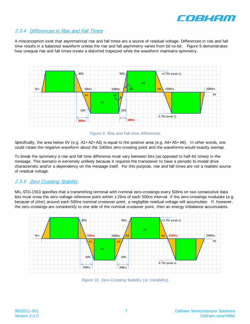
2.3.4 Differences in Rise and Fall Times
A misconception exist that asymmetrical rise and fall times are a source of residual voltage. Differences in rise and fall time results in a balanced waveform unless the rise and fall asymmetry varies from bit-to-bit. Figure 9 demonstrates how unequal rise and fall times create a distorted trapezoid while the waveform maintains symmetry.
Figure 9. Rise and Fall time differences
Specifically, the area below 0V (e.g. A1+A2+A3) is equal to the positive area (e.g. A4+A5+A6). In other words, one could rotate the negative waveform about the 1000ns zero-crossing point and the waveforms would exactly overlap.
To break the symmetry a rise and fall time difference must vary between bits (as opposed to half-bit times) in the message. This scenario is extremely unlikely because it requires the transceiver to have a periodic bi-modal drive characteristic and/or a dependency on the message itself. For this purpose, rise and fall times are not a realistic source of residual voltage.
2.3.5 Zero Crossing Stability
MIL-STD-1553 specifies that a transmitting terminal with nominal zero-crossings every 500ns on two consecutive data bits must cross the zero-voltage reference point within ±25ns of each 500ns interval. If the zero-crossings modulate (e.g. because of jitter) around each 500ns nominal crossover point, a negligible residual voltage will accumulate. If, however, the zero crossings are consistently to one side of the nominal crossover point, then an energy imbalance accumulates.
Figure 10. Zero-Crossing Stability (or Instability)
0V
A4 A6
A5
A1
A2
A3
90%
10%
0ns 500ns 1000ns 1500ns 2000ns
90%
10%
200ns 100ns
+3.75V peak-LL
-3.75V peak-LL
0V
A4 A6
A5
A1
A2
A3
90%
10%
0ns 525ns 1000ns 1525ns 2000ns
90%
10%
200ns 200ns
+3.75V peak-LL
-3.75V peak-LL

9502011-001 8 Cobham Semiconductor Solutions Version 2.0.0 Cobham.com/HiRel
Figure 10 illustrates a MIL-STD-1553 waveform with nominal 500ns bit transitions where each positive pulse is 25ns longer than the ideal 500ns pulse width. Consequently, the negative pulse is 25ns shorter than ideal. The total positive pulse width minus the negative pulse width is 50ns. The area associated with this 50ns difference results in a proportional residual voltage.
2.4 Summary on Background Residual Voltage Discussion
The exaggerated asymmetries depicted in Figures 6-10 are often much more subtle on a bit-by-bit basis. Furthermore, the isolated, well-balanced, closed-loop nature of the MIL-STD-1553 bus results in a natural self-zeroing behavior on the bus, making it difficult to notice asymmetries. That said, non-idealities in the real world inevitably create a non-zero residual voltage on the MIL-STD-1553 bus following any transmission.
The remainder of this product advisory focuses on the findings from a residual voltage problem investigation, which focuses on transceiver-transformer interaction that appears to correlate well with residual voltage.
3.0 Major Investigation Findings
The investigation team isolated the anomalistic residual voltage to an interaction between the transceiver and transformer. All other likely factors such as power supply decoupling, board layout, clock integrity, assembly defects (e.g. cold solder joints), and bus side connector and cable harnessing were disqualified as significant residual voltage contributors in the application and board design.
The investigation team reduced the MIL-STD-1553 network to a minimal set of components – protocol, transceiver, transformer, and load resistor. A pair of oscilloscope probes were attached in a single-ended fashion to the primary terminals of the transformer while a second set of probes were connected differentially across the load resistor. The protocol device transmitted a 32-word message using a valid VOS test pattern described in MIL-STD-1553 section 4.5.2.2.1.4. The investigation team captured the signal characteristics on the primary side during the transmission and recorded the associated residual voltage across the resistor. Figure 11 depicts the single-ended measurement configuration for this portion of the investigation and Figure 12 shows the associated waveforms and measurements.
Figure 11. Test Configuration Used to Evaluate Transceiver-Transformer Interactions
The waveforms on the isolation transformer primary terminals had a large amount of ringing. The blue waveform shows the TXOUT signal from the transceiver while the brown trace represents the TXOUT# signal. Therefore, the half-bit depicted on the left side of Figure 12 is a differential LOW pulse followed by the differentially positive half bit which occurs when the blue waveform rises. The distinctly different wave-shapes for each half bit are demonstrable evidence of asymmetric leakage inductances in the transformer’s positive and negative windings. The transformer’s bandwidth blocks the high frequency oscillations from reaching the secondary side of the transformer. Consequently, the blocked energy is lost – dissipated as heat in the system. Since the amount of energy blocking is different for each half-bit, a corresponding residual voltage arises reflecting the unequal energy transfer to the secondary side of the transformer. Proof of this asymmetry is shown by the right side of Figure 12, where the secondary side of the isolation transformer exhibits -260mV (-10mV below spec) of residual voltage at conclusion of the transmission.

9502011-001 9 Cobham Semiconductor Solutions Version 2.0.0 Cobham.com/HiRel
Figure 12. (Left) Waveforms on Primary Side of Isolation Transformer (Right) Final Residual Voltage on Secondary Side of Isolation Transformer (10mV below MIL-STD-1553 Specification Limit)
Armed with the observations from Figure 12, the investigation team proceeded to evaluate a variety of transformers from several vendors to validate its hypothesis that primary side leakage inductance imbalances are the leading factor to half-bit asymmetries and are the main source of residual voltages. Table 2 lists five transformers used in the analysis along with the leakage inductance for each transformer and the resulting residual voltage when each transformer interfaced to a single Cobham UT69151-DXE protocol+transceiver module.
Table 2. Sample Transformers from Evaluation with Primary Leakage Inductance and Residual Voltage Measurements
Manufacturer Transformer SN
Vr Leakage Inductance
L1-2 µH's
pin 5-pin 7 shorted
all other pins open
Leakage Inductance
L2-3 µH's
pin 5-pin 7 shorted
all other pins open
Leakage Inductive Imbalance
(L1-2 - L2-3) µH's
% of
Leakage Inductance Imbalance
Vendor X 005 -41mV 0.469 0.314 0.155 20%
Vendor X 069 +39mV 0.295 0.436 -0.141 19%
Vendor X 207 +7mV 0.251 0.247 0.004 1%
North Hills A +12mV 0.411 0.385 0.026 3%
Pulse 586 +12mV 0.187 0.197 0.010 3%
Table 2 includes 3 transformers from the customer’s selected vendor along with one transformer each from Cobham’s recommended vendors – Pulse Electronics and North Hills Signal Processing Corp. Cobham has generally recommended Pulse and North Hills transformers because these are the two suppliers whose transformers Cobham used in the development of the transceivers listed in Table 1. Furthermore, it is the Pulse Electronics transformer that Cobham uses in the production testing of its transceiver. Due to the long proven history of Pulse and North Hill transformers in

9502011-001 10 Cobham Semiconductor Solutions Version 2.0.0 Cobham.com/HiRel
successful MIL-STD-1553 network implementations, Cobham strongly recommends the use of these two transformer vendors.
Notice the column indicating the residual voltage measured with each transformer when interfaced to a single UT69151-DXE in Table 2. In addition to the residual voltages, the last column lists the percentage of differential inductance mismatch for each transceiver. Comparing the two columns, one can see a relationship between the amount of inductive mismatch and the associated residual voltage. Figures 13 through 17 present the oscilloscope plots for each of the transformers in Table 2 interfacing to channel A on the same UT69151-DXE module.
The scope probes were connected to pins 1 and 3 on the transformer as depicted in Figure 11. Referencing the plots in Figures 13 through 17, the PINK trace is TXOUT and the GREEN trace is TXOUT#. The PURPLE trace is the mathematical addition of the TXOUT and TXOUT# signals. This is not differential addition, which would result in the conventional looking MIL-STD-1553 pp-ll waveforms. Instead, the addition of the two signals is intended to illustrate the amount of differential imbalance in the waveforms. If the waveforms were exactly balanced, the PURPLE trace would be exactly 0V throughout the measurement. More importantly, a difference in the total area beneath the PUPLE curve for each half-bit is indicative of the meaningful asymmetry that creates a residual voltage.
Since the PURPLE waveform during subsequent half-bit times is not identical, an imbalance is present. As a word of caution, the oscilloscope statistics shown in the following plots do not show the Delta-volts/Delta-time measurements for each half pulse. Therefore, you cannot quantitatively extrapolate the half-bit differences from these plots. However, the half-bit imbalances are sufficiently obvious to illustrate the relationship between these waveforms and their associated residual voltages.
Figure 13. TXOUT & TXOUT symmetry between UT69151-DXE CHA and Vendor X SN005
Vendor X SN005 / Inductance Mismatch = 20% / VR = -41mV p-LL

9502011-001 11 Cobham Semiconductor Solutions Version 2.0.0 Cobham.com/HiRel
Figure 14. TXOUT & TXOUT symmetry between UT69151-DXE CHA and Vendor X SN069
Figure 15. TXOUT & TXOUT symmetry between UT69151-DXE CHA and Vendor X SN207
Vendor X SN207 / Inductance Mismatch = 1% / VR = +7mV
Vendor X SN069 / Inductance Mismatch = 19% / VR = +39mV

9502011-001 12 Cobham Semiconductor Solutions Version 2.0.0 Cobham.com/HiRel
** Note: The oscilloscope setup for the North Hills transformer experiment in Figure 16 represents the initial configuration. The remaining transformer experiments are subsequent to Figure 16 and reflect a higher sample rate and better display organization.
Figure 16. TXOUT & TXOUT symmetry between UT69151-DXE CHA and North Hills SN A
Figure 17. TXOUT & TXOUT symmetry between UT69151-DXE CHA and Pulse SN586
Pulse Electronics (SN586) / Inductance Mismatch = 3% / VR = +12mV
North Hills (SN A) / Inductance Mismatch = 3% / VR = +12mV

9502011-001 13 Cobham Semiconductor Solutions Version 2.0.0 Cobham.com/HiRel
Qualitatively, the Pulse brand transformer has the least distorted response to the UT69151-DXE transceiver interface. The North Hills transformer also has a good response to Cobham’s transceiver. Vendor X’s transformers, on the other hand, have a very inconsistent response. SN207 for example resulted in the lowest residual voltage of the five samples and exhibited a small amount of primary side signal distortion on par with the North Hills. However, the other two transformers from Vendor X exhibit a poor interaction with the UT69151-DXE transceiver and result in the highest degree of residual voltage. Note that the waveform and residual voltage seen in Figure 12 was produced by a fourth transformer from Vendor X.
Leakage inductance mismatch between the positive and negative legs on the primary side of the transformer is a major contributor to residual voltage. However, the correlation factor is still unclear. Transformers have additional characteristics that are not listed in the product specifications and are not readily extracted from parametric measurements of the transformers (i.e. permeability of the core material, reflected impedance mismatches, manufacturing techniques, etc.). Each of these plays a role in the compatibility between transceiver and transformer and their ability to efficiently transfer energy in a balanced way. Ultimately, the degree of “ringing” and asymmetry in successive half-bit times, as measured by signal distortion and voltage area analysis, is the best method to determine if a terminal is going to leave an unnecessarily high residual voltage on the MIL-STD-1553 data bus.
4.0 Recommendations
Cobham recommends that system designers continue to use Pulse, North Hills, or BTTC (see Appendix C) transformers for interfacing with Cobham transceivers. We also recommend additional parametric screening for transformers with an acceptance preference for transformers having <20% relative differential leakage inductance. Transformer datasheets exclude many relevant parameters as shown in the Pulse Electronics specification for the 1553-45 transformer in Appendix A of this advisory. Appendix B presents parametric screening gathered by Cobham engineers when characterizing transformers beyond what is gleaned from the manufacturer’s specification. The data contained in Appendix B is data measured on the Pulse 1553-45 transformer.
Cobham also recommends an evaluation of primary side signal integrity and half-bit time balance vs. residual voltage during brass board and engineering model checkout. If the circuit board uses a transformer vendor other than Pulse or North Hills, Cobham strongly encourages the system designer to perform a compatibility analysis.
5.0 Conclusion
The system designer must consider many important factors when implementing a MIL-STD-1553 terminal. Achieving optimal performance and compliance to MIL-STD-1553 is a function of the components employed (e.g. clocking, protocol handler, transceiver, transformer, and connectors) as-well-as circuit implementation decisions such as board layout, ground planes, signal routing and decoupling. This product advisory focuses the component-driven contribution to residual voltage in a MIL-STD-1553 network and discusses how to minimize it through wise component selection.
Cobham made efforts to correlate residual voltage with leakage inductance, primary and secondary side inductance, and winding resistance of various transformers. Within the closed-loop system of the MIL-STD-1553 protocol device, all of the parameters interact with each other, often times cancelling the unbalancing effects of each other. For this reason, no single parametric characteristic precisely predicts residual voltage. Apart from the parametric characteristics that are readily measurable, manufacturing techniques and materials employed by the various manufacturers also affect transformer performance.
Although it is difficult to ascertain the exact parameter that will eliminate residual voltage for a given MIL-STD-1553 terminal, the investigation team found leakage inductance to be the most predictive parametric indicator of residual voltage. The presence of leakage inductance is most evident when evaluating signal integrity of the waveforms on the primary side of the isolation transformers. Measuring signal quality on the primary side of the isolation transformer is a high fidelity indicator of inefficient and/or imbalanced energy transfer onto point A of the MIL-STD-1553 bus.
Using proven transformer vendors who have a demonstrated history of reliable, problem free, interoperation with the selected transceivers affords the system designer the highest probability of success. For the purpose of matching transformers to the Cobham components listed in Table 1, Pulse Electronics (http://www.pulseelectronics.com ), North Hills Signal Processing Corp. (http://www.nhsignal.com), and per Appendix C, BTTC (http://bttc-beta.com) are proven MIL-STD-1553 transformer suppliers.
9502011-001 14 Cobham Semiconductor Solutions Version 2.0.0 Cobham.com/HiRel
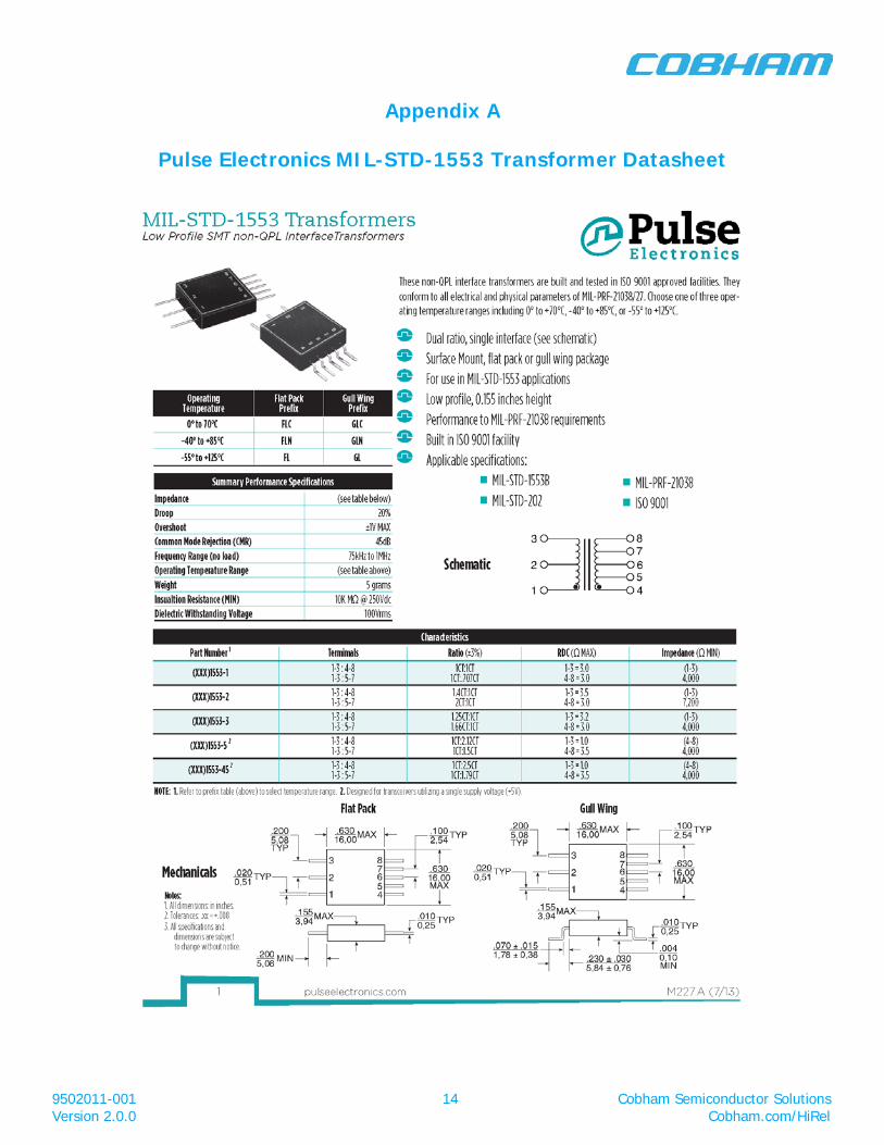
Appendix A
Pulse Electronics MIL-STD-1553 Transformer Datasheet

9502011-001 15 Cobham Semiconductor Solutions Version 2.0.0 Cobham.com/HiRel

9502011-001 16 Cobham Semiconductor Solutions Version 2.0.0 Cobham.com/HiRel
Appendix B
Cobham Parametric Test Data on a Single Pulse 1553-45
1553-45 TRANSFORMERIMPEDANCE INDUCTANCE UNITS
Z1-3 4-8 OPEN L1-3 4.22 mHFREQ, KHZ MAG Z, KΩ ANGLE Z, DEGREES L4-8 23.69 mH
75 1.857 55 L1-2 1.14 mH100 2.562 46 L2-3 1.14 mH200 7.936 2.4 L7-5 12.37 mH269 13.000 0 4-8 SHORTED300 11.660 -34 LL1-2 0.105 uH400 6.420 -53 LL2-3 0.108 uH500 4.337 -64 LL1-3 0.358 uH600 3.312 -70 7-5 SHORTED uH700 2.700 -74 LL1-2 0.171 uH800 2.288 -77 LL2-3 0.181 uH900 1.992 -79 TURNS RATIO1000 1.767 -80 L1-3/4-8 2.369
L1-2/4-8 4.559L2-3/4-8 4.559
5-7 70 OHM TERM Z 1-2 Z 2-3 L1-3/7-5 1.712FREQ, KHZ MAG Z, OHMS MAG Z, OHMS L1-2/7-5 3.294
75 5.828 5.827 L2-3/7-5 3.294500 5.873 5.879 DC RESISTANCE1000 5.992 6.013 L1-3 0.466 Ohms
L1-2 0.228 Ohms4-8 140 OHM TERM Z 1-2 Z 2-3 L2-3 0.243 Ohms
FREQ, KHZ MAG Z, OHMS MAG Z, OHMS L4-8 2.61 Ohms75 5.941 5.938 L7-5 1.68 Ohms
500 5.967 5.9631000 6.038 6.032
5.7
5.75
5.8
5.85
5.9
5.95
6
6.05
75 500 1000
Z ohms
FREQUENCY, KHZ
Z1-2, Z2-3 REFLECTED Z w/ 5-7 term 70 ohms
MAG Z, OHMS
MAG Z, OHMS
9502011-001 17 Cobham Semiconductor Solutions Version 2.0.0 Cobham.com/HiRel
Appendix C
Compatibility Summary for BTTC-Beta Transformers
C.1 Introduction
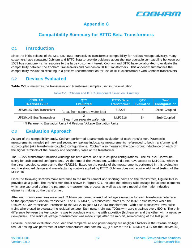
Since the initial release of the MIL-STD-1553 Transceiver/Transformer compatibility for residual voltage advisory, many customers have contacted Cobham and BTTC-Beta to provide guidance about the interoperable compatibility between our 1553 bus components. In response to the large customer interest, Cobham and BTTC have collaborated to evaluate the compatibility between the Cobham Transceivers and companion BTTC Transformers. This appendix summarizes the compatibility evaluation resulting in a positive recommendation for use of BTTC transformers with Cobham transceivers.
C.2 Devices Evaluated
Table C-1 summarizes the transceiver and transformer samples used in the evaluation.
Table C-1. Cobham and BTTC Component Selection Summary
COBHAM TRANSCEIVER
QTY Evaluated
BTTC-Beta Transformer
QTY Evaluated
Test Configuration
UT63M147 Bus Transceiver 2 (1 ea. from separate wafer lots) B-3227 5 Direct-Coupled
UT63M143 Bus Transceiver 2 (1 ea. from separate wafer lots MLP2216 5* Stub-Coupled
* 5 Parametric Evaluation Units / 4 Residual Voltage Evaluation Units
C.3 Evaluation Approach
As part of the compatibility study, Cobham performed a parametric evaluation of each transformer. Parametric measurements included primary and secondary leakage inductance measurements; referenced to both transformer and stub-coupled (aka transformer-coupled) configurations. Cobham also measured the open circuit inductance on each of the signal terminals of the primary and secondary sides of the transformer.
The B-3227 transformer included windings for both direct- and stub-coupled configurations. The MLP2216 is wound solely for stub-coupled configurations. At the time of the evaluation, Cobham did not have access to MLP2016, which is the direct-coupled counterpart to the MLP2216. Based on the results of the measurements performed in this evaluation and the standard design and manufacturing controls applied by BTTC, Cobham does not require additional testing of the MLP2016.
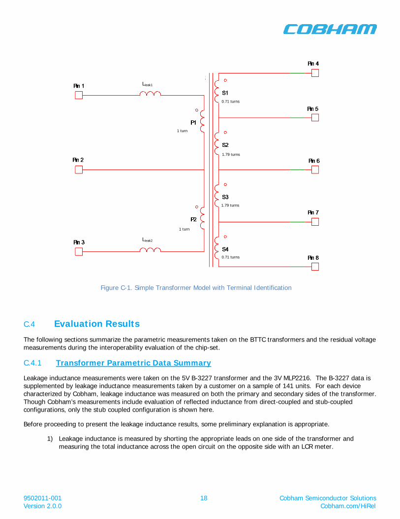
Since the following sections make reference to the measurement and shorting points on the transformer, Figure C-1 is provided as a guide. The transformer circuit shown in Figure C-1 includes the primary-side leakage inductance elements which are captured during the parametric measurement process, as well as a simple model of the major inductive elements making up the transformer.
After each transformer was measured, Cobham performed a residual voltage evaluation for each transformer interfaced to the appropriate Cobham transceiver. The UT63M147, 5V transceiver, mates to the B-3227 transformer while the UT63M143, 3V transceiver, interfaces to the MLP2216 (and MLP2016) transformers. With each transceiver, two pulse trains where used to evaluate the residual voltage. Each pulse train was 700µs with zero crossings every 500ns. The only difference between the test patterns was to conclude one string with a positive (high-pulse) and the other with a negative (low-pulse). The residual voltage measurement was made 2.5µs after the mid-bit, zero-crossing of the last pulse.
Because, previous evaluation concluded that temperature and power-supply are negligible factors in the residual voltage test, all testing was performed at room temperature and nominal VDD (i.e. 5V for the UT63M147; 3.3V for the UT63M143).
9502011-001 18 Cobham Semiconductor Solutions Version 2.0.0 Cobham.com/HiRel
C.4 Evaluation Results
The following sections summarize the parametric measurements taken on the BTTC transformers and the residual voltage measurements during the interoperability evaluation of the chip-set.
C.4.1 Transformer Parametric Data Summary Leakage inductance measurements were taken on the 5V B-3227 transformer and the 3V MLP2216. The B-3227 data is supplemented by leakage inductance measurements taken by a customer on a sample of 141 units. For each device characterized by Cobham, leakage inductance was measured on both the primary and secondary sides of the transformer. Though Cobham’s measurements include evaluation of reflected inductance from direct-coupled and stub-coupled configurations, only the stub coupled configuration is shown here.
Before proceeding to present the leakage inductance results, some preliminary explanation is appropriate.
1) Leakage inductance is measured by shorting the appropriate leads on one side of the transformer and measuring the total inductance across the open circuit on the opposite side with an LCR meter.
Lleak1
Lleak2
1 turn
1.79 turns
0.71 turns
1.79 turns
0.71 turns
1 turn
Figure C-1. Simple Transformer Model with Terminal Identification
9502011-001 19 Cobham Semiconductor Solutions Version 2.0.0 Cobham.com/HiRel
a. For the Cobham measured data in the section below, the measurement equipment was:
i. Keysight E4980A ii. Measurement setting: Lp-D iii. Signal Frequency: 1MHz iv. Signal Amplitude: 100mA
2) Measuring the leakage inductance on the primary side of the transformer includes the “real” leakage inductance plus a small inductive contribution for the non-ideal short on the secondary side of the transformer, which is reflected to the primary side by the square of the turns ratio. [1]
a. When calculating the differential leakage, the shorting inductance error cancels out.
3) Using the BTTC test method [2] to measure leakage inductance on the secondary side of the transformer results in a reflected leakage inductance that is transformed by the turns ratio squared.
a. Referencing Figure C-1, the transform equation is:
𝐸𝐸1. 𝐿𝐿𝐿𝐿𝑘1′ = 𝐿𝐿𝐿𝐿𝑘1 ∗ 𝑆2 + 𝑆3𝑃1
2
Where Lleak1’ is the reflected leakage inductance measured across the secondary windings of the transformer. Lleak1 is the “real” leakage inductance on the positive or negative signal winding of the primary side. S2 and S3 are the secondary windings which make up the desired turns ratio for a transformer-coupled interface. P1 is the primary side winding for the positive half of the complementary signals on the 1553 transceiver. P1 and P2 are ideally equal.
4) Applying EQ1 to the empirical measurements presented in the data will yield a ‘close’ but not exact match. The reason for this inexact result is due to non-ideal characteristics of the transformer (e.g. turns ratio tolerance) and from imperfections in the measurement system (e.g. imperfect short circuit, LCR contact resistance, measurement point on the transformer leads, repeatability tolerance of the measurement, etc.)
a. The leakage inductances in columns 2, 3, 6 and 7 of the following tables, include a small positive error because a perfect short was not possible and the location of the short and LCR probe points was not exactly repeatable.
b. Cobham took care to short and measure each transformer in a consistent manner, but practical limitations (e.g. human variability) necessarily increase the magnitude of measured inductances and, to the extent that identical conditions where not achieved when measuring Lleak1 vs Lleak2, a proportional error comes out in the differential leakage inductance calculations.
5) The parametric tables, below, are organized in a quadrant format.
a. The first four data columns are associated with “real” leakage inductance measured on the primary side of the transformer.
b. The last four data columns cover reflected leakage inductance measured on the secondary side of the transformer.
c. The first five data rows present the data taken for each transformer in the sample set.
d. The next 7 rows are basic statistical calculations of the sample data.
i. Do not try to calculate differential (delta) leakage values from the statistical calculations because differential results must be determined on a part-by-part basis.

9502011-001 20 Cobham Semiconductor Solutions Version 2.0.0 Cobham.com/HiRel
e. The last row provides BTTC’s leakage inductance spec limits [2].
f. The % of Differential Leakage Inductance values are based upon the specific leakage inductances measured for the individual devices; not against BTTC’s absolute limit for differential leakage inductance.
i. Based upon Cobham’s residual voltage studies, a relative % of differential leakage inductance that is < 20% is sufficiently low to have a limited impact on residual voltage. The relative % of differential leakage inductance is calculated as:
𝐸𝐸2. 𝑅𝐿𝐿𝐿𝑅𝑅𝑅𝐿 %∆ 𝐿𝐿𝐿𝐿𝑘 = 𝐿𝐿𝐿𝐿𝑘1 − 𝐿𝐿𝐿𝐿𝑘2𝐿𝐿𝐿𝐿𝑘1 + 𝐿𝐿𝐿𝐿𝑘2
∗ 100
Where Lleak1 is the leakage inductance for the positive signal windings on the primary side of the transformer and LLeak2 is the leakage inductance for the complementary negative signal winding.
C.4.1.1 B-3227 Leakage Inductance Analysis Table C-2 reflects the data measured by Cobham on the BTTC B-3227 transformer. The sample size was five (n=5). The following are take-aways from the table:
• The magnitude of leakage inductance on all devices (columns 2, 3, 6, and 7) is less than the Beta limit of 6uH (468nH primary side).
• The 3-sigma calculation for leakage inductances all have positive margin to their respective upper spec limits, with differential leakage inductance having the lowest margin.
Table C-2. BTTC B-3227 Leakage Inductance Parametric Data Summary
BTTC B-3227
n=5
Leakage Inductance Measured on Primary Side Leakage Inductance Measured on Secondary Side
Leakage Inductance
LL1 (nH) (Short 5-7 /
Measure 1-2)
Leakage Inductance
LL2 (nH) (Short 5-7 /
Measure 2-3) Delta (nH) (LL1-LL2)
% of Differential
Leakage Inductance
Leakage Inductance
LL1 (µH) (Short 1-2 /
Measure 5-7)
Leakage Inductance
LL2 (µH) (Short 2-3 /
Measure 5-7) Delta (µH) (LL1-LL2)
% of Differential
Leakage Inductance
SN1 282.450 257.370 25.080 4.65% 3.620 3.180 0.440 6.47% SN2 266.340 272.890 -6.550 -1.21% 3.400 3.450 -0.050 -0.73% SN3 282.910 262.560 20.350 3.73% 3.630 3.320 0.310 4.46% SN4 309.120 269.420 39.700 6.86% 3.890 3.430 0.460 6.28% SN5 286.430 290.300 -3.870 -0.67% 3.620 3.680 -0.060 -0.82% Min 266.340 257.370 -6.550 -1.21% 3.400 3.180 -0.060 -0.82% Max 309.120 290.300 39.700 6.86% 3.890 3.680 0.460 6.47% Mean 285.450 270.508 14.942 2.67% 3.632 3.412 0.220 3.13%
Std Dev 15.345 12.593 19.753 3.49% 0.174 0.184 0.258 3.65% 3σ margin to Upper
Limit 136.7 159.86 3.829 6.86% 1.846 2.032 .006 5.92%
Upper Spec Limit 468.15 468.15 78.03 20% 6.00 6.00 1.00 20%
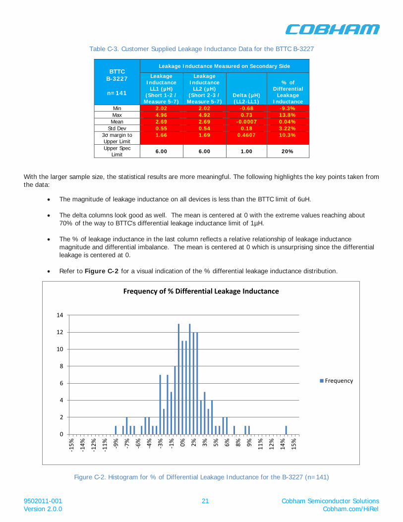
Only for the case of the B-3227 transformer did Cobham obtain supplemental leakage inductance data from a customer. The customer measured leakage inductance on 141 units (n=141). The statistical results of the customer’s data are shown in Table C-3. The measurements were only taken on the secondary side of the transformer using the BTTC preferred measurement technique.
9502011-001 21 Cobham Semiconductor Solutions Version 2.0.0 Cobham.com/HiRel
Table C-3. Customer Supplied Leakage Inductance Data for the BTTC B-3227
BTTC B-3227
n=141
Leakage Inductance Measured on Secondary Side
Leakage Inductance
LL1 (µH) (Short 1-2 /
Measure 5-7)
Leakage Inductance
LL2 (µH) (Short 2-3 /
Measure 5-7) Delta (µH) (LL2-LL1)
% of Differential
Leakage Inductance
Min 2.02 2.02 -0.68 -9.3% Max 4.96 4.92 0.73 13.8% Mean 2.69 2.69 -0.0007 0.04%
Std Dev 0.55 0.54 0.18 3.22% 3σ margin to Upper Limit
1.66 1.69 0.4607 10.3%
Upper Spec Limit 6.00 6.00 1.00 20%
With the larger sample size, the statistical results are more meaningful. The following highlights the key points taken from the data:
• The magnitude of leakage inductance on all devices is less than the BTTC limit of 6uH.
• The delta columns look good as well. The mean is centered at 0 with the extreme values reaching about 70% of the way to BTTC’s differential leakage inductance limit of 1µH.
• The % of leakage inductance in the last column reflects a relative relationship of leakage inductance
magnitude and differential imbalance. The mean is centered at 0 which is unsurprising since the differential leakage is centered at 0.
• Refer to Figure C-2 for a visual indication of the % differential leakage inductance distribution.
Figure C-2. Histogram for % of Differential Leakage Inductance for the B-3227 (n=141)
0
2
4
6
8
10
12
14
-15%
-14%
-12%
-11% -9
%
-7%
-6%
-4%
-3%
-1% 0% 2% 3% 5% 6% 8% 9% 11%
12%
14%
15%
Frequency of % Differential Leakage Inductance
Frequency

9502011-001 22 Cobham Semiconductor Solutions Version 2.0.0 Cobham.com/HiRel
C.4.1.2 MLP-2216 Leakage Inductance Analysis Table C-4 presents the parametric measurements that Cobham took from five samples of the MLP-2216 transformer. The same approach taken to measure and analyze leakage inductance on the B-3227 transformer (reference Table C-2) was used to evaluate the MLP-2216 transformer.
The MLP-2216 has a primary:secondary turns ratio of 1:2.15 for stub-coupled configurations. Based on BTTC empirical measurements, the primary side leakage inductance for the MLP-2x16 is 486.75nH (9uH when reflected to the secondary side) with a differential leakage inductance of 81.12nH (1.5uH when reflected to the secondary side). These values represent the BTTC upper specification limits for the MLP-2x16 transformers.
Table C-4. BTTC MLP-2216 Leakage Inductance Parametric Data Summary
BTTC MLP2216
n=5
Leakage Inductance Measured on Primary Side Leakage Inductance Measured on Secondary Side
Leakage Inductance
LL1 (nH) (Short 5-7 /
Measure 1-2)
Leakage Inductance
LL2 (nH) (Short 5-7 /
Measure 2-3) Delta (nH) (LL1-LL2)
% of Differential
Leakage Inductance
Leakage Inductance
LL1 (µH) (Short 1-2 /
Measure 5-7)
Leakage Inductance
LL2 (µH) (Short 2-3 /
Measure 5-7) Delta (µH) (LL1-LL2)
% of Differential
Leakage Inductance
SN1 122.98 121.08 1.90 0.78% 2.31 2.15 0.16 3.59% SN2 113.67 121.03 -7.36 -3.14% 2.12 2.15 -0.03 -0.70% SN3 129.62 129.68 -0.06 -0.02% 2.42 2.41 0.01 0.21% SN4 130.82 126.40 4.42 1.72% 2.44 2.34 0.10 2.09% SN5 123.37 107.32 16.05 6.96% 2.34 2.12 0.22 4.93% Min 113.670 107.320 -7.360 -3.14% 2.120 2.120 -0.030 -0.70% Max 130.820 129.680 16.050 6.96% 2.440 2.410 0.220 4.93% Mean 124.092 121.102 2.990 1.26% 2.326 2.234 0.092 2.02%
Std Dev 6.823 8.538 8.518 3.67% 0.127 0.132 0.103 2.33% 3σ margin to Upper Limit 342.189 339.284 52.58 7.73% 6.293 6.37 1.099 10.99%
Upper Spec Limit
486.75 486.75 81.12 20% 9.00 9.00 1.50 20%
The results of parametric measurements on the MLP-2216 are very good. The total leakage inductance is very low, provide several hundred nH of margin after accounting for 3-sigma in variation. Similarly, the differential leakage inductance when evaluated as a percentage and absolute value, with 3-sigma variation considered, is about 2/3rds the BTTC upper spec limit. Parametrically speaking, the BTTC MLP-2216 has very low leakage inductance.
C.4.2 Residual Voltage (Vr) Demonstration The BTTC transformers were mated with companion Cobham transceivers. Two different 5V UT63M147 transceivers were used to evaluate residual voltage with each of the B-3227 transformers. Similarly, two different 3V UT63M143 transceivers were used to evaluate residual voltage with each MLP-2216 transformer. Using both transceivers, a Vr measurement was taken for both positive and negative ending pulses.
The next couple sections present residual voltage results from Cobham’s evaluation.
C.4.2.1 B-3227 & UT63M147 Residual Voltage Results A direct-coupled bus configuration was used for B-3227/UT63M147 residual voltage tests. A concluding LOGIC 1 parity bit results in a negative ending pulse whose resulting Vr is more positive than the LOGIC 0 parity, which concludes with a positive pulse.

9502011-001 23 Cobham Semiconductor Solutions Version 2.0.0 Cobham.com/HiRel
Table C-5. Residual Voltage Results for B-3227 and UT63M147 Chip Sets
5962*9322603*** XFMR: B-3227 Direct Coupled Configuration. Vr limit = +/- 9E-02 V XCVR SN 70 XCVR SN 70 XCVR SN 1 XCVR SN 1
Parity bit 0 Parity Bit 1 Parity Bit 0 Parity Bit 1 N = 5 5 5 5 SN1 -1.37E-02 1.29E-02 -3.99E-03 6.25E-03 SN2 -3.37E-03 1.53E-02 -5.25E-03 7.50E-03 SN3 -9.62E-03 1.15E-02 -7.87E-03 3.87E-03 SN4 -1.43E-02 7.50E-03 -1.31E-02 0.00E+00 SN5 -5.75E-03 2.16E-02 -4.12E-03 8.87E-03
Vr Min (V) -1.43E-02 7.50E-03 -1.31E-02 0.00E+00 Vr Max (V) -3.37E-03 2.16E-02 -3.99E-03 8.87E-03
Vr Mean (V) -9.34E-03 1.37E-02 -6.87E-03 5.30E-03 Vr Std Dev (V) 4.79E-03 5.22E-03 3.83E-03 3.49E-03
margin to +90mV Spec Lim. 20.74 σ 14.62 σ 25.29 σ 24.27 σ
margin to -90mV Spec Lim. 16.84 σ 19.87 σ 21.7 σ 27.31 σ
The most important take-away from the Vr results is the significant margin the chip set has relative to the ±90mV MIL-STD-1553 direct-coupled Vr limit. These results demonstrate very good compatibility between the UT63M147 and B-3227, culminating in a low residual voltage.
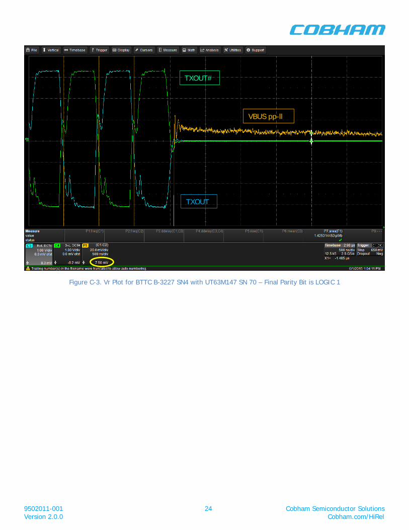
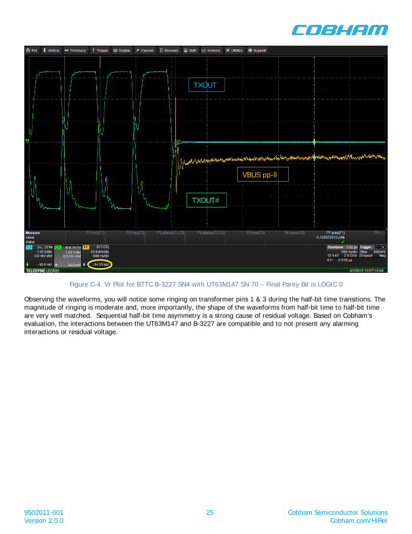
Figure C-3 and Figure C-4 depict the residual voltage waveform measured on B-3227 SN4 and UT63M147 SN70 for the LOGIC 1 and LOGIC 0 parity bits, respectively. The GREEN and BLUE waveforms are measured on the primary side of the transformer. The ORANGE trace is the differential voltage measured across the 1553 databus (pins 5 and 7). The resolution setting for the bus waveform is set to 20mV/division.
9502011-001 24 Cobham Semiconductor Solutions Version 2.0.0 Cobham.com/HiRel
Figure C-3. Vr Plot for BTTC B-3227 SN4 with UT63M147 SN 70 – Final Parity Bit is LOGIC 1
TXOUT
TXOUT#
VBUS pp-ll
9502011-001 25 Cobham Semiconductor Solutions Version 2.0.0 Cobham.com/HiRel
Figure C-4. Vr Plot for BTTC B-3227 SN4 with UT63M147 SN 70 – Final Parity Bit is LOGIC 0
Observing the waveforms, you will notice some ringing on transformer pins 1 & 3 during the half-bit time transitions. The magnitude of ringing is moderate and, more importantly, the shape of the waveforms from half-bit time to half-bit time are very well matched. Sequential half-bit time asymmetry is a strong cause of residual voltage. Based on Cobham’s evaluation, the interactions between the UT63M147 and B-3227 are compatible and to not present any alarming interactions or residual voltage.
TXOUT
TXOUT#
VBUS pp-ll

9502011-001 26 Cobham Semiconductor Solutions Version 2.0.0 Cobham.com/HiRel
C.4.2.2 MLP-2216 & UT63M143 Residual Voltage Results A stub-coupled bus configuration was used for MLP-2216/UT63M143 residual voltage tests. A concluding LOGIC 1 parity bit results in a negative ending pulse whose resulting Vr is more positive than LOGIC 0 parity which concludes with a positive pulse. For the MLP-2216, all Vr measurements ended in a positive voltage. However, the LOGIC 1 parity bit was always higher potential than the corresponding LOGIC 0 parity bit. The results of Cobham’s Vr measurements on the MLP-2216 are shown in Table C-6.
The MLP-2216 transformers are low-profile, fine pitched, surface mount transformers. To take inductance measurements and to insert the transformers into Cobham’s test board, lead extensions where added to the MLP-2216 terminals. During the course of residual voltage testing, serial number 2 and 5 broke at the lead interface to the molded plastic encapsulation. Consequently, we were unsuccessful obtaining two sets of Vr measurements for all 5 MLP-2216 devices originally allocated to the study.
Table C-6. Residual Voltage Results for MLP-2216 and UT63M143 Chip Sets
5962*0724201***
XFMR: MLP2216 Stub-Coupled Configuration. Vr limit = +/-2.50E-01 V XCVR SN 29 XCVR SN 29 XCVR SN 19 XCVR SN 19 Parity bit 0 Parity Bit 1 Parity Bit 0 Parity Bit 1
N= 4 4 3 3 SN1 1.58E-02 4.87E-02 1.24E-02 3.89E-02 SN2 1.66E-02 4.51E-02 NL NL SN3 7.87E-03 3.26E-02 8.50E-03 3.73E-02 SN4 4.12E-03 4.37E-02 1.28E-02 4.42E-02 SN5 NL NL NL NL
Vr Min (V) 3.26E-02 4.12E-03 3.73E-02 8.50E-03 Vr Max (V) 4.87E-02 1.66E-02 4.42E-02 1.28E-02
Vr Mean (V) 4.26E-02 1.11E-02 4.01E-02 1.12E-02 Std Dev (V) 6.95E-03 6.09E-03 3.66E-03 2.35E-03
margin to +250mV Spec Lim. 29.84 σ 39.22 σ 57.34 σ 101.62 σ
margin to -250mV Spec Lim. 36.58 σ 42.87 σ 79.26 σ 111.15 σ
Similar to the results from the B-3227, the most important take-away from the MLP-2216 Vr results is the significant margin the chip set has relative to the ±250mV MIL-STD-1553 stub-coupled Vr limit. These results demonstrate very good compatibility between the UT63M143 and MLP-2216, culminating in a low residual voltage.
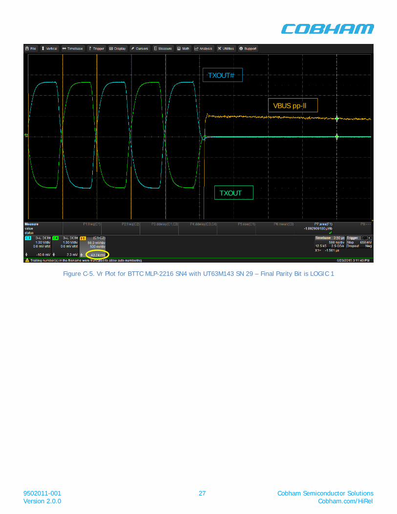
Figure C-5 and Figure C-6 present the residual voltage waveform measured on MLP-2216 SN4 and UT63M143 SN29 for the LOGIC 1 and LOGIC 0 parity bits, respectively. The GREEN and BLUE waveforms are measured on the primary side pins of the transformer. The ORANGE trace is the differential voltage measured across the 1553 databus. The resolution setting for the bus waveform is set to 50mV/division in Figure C-5 and 20mV/div in Figure C-6. The resolution was adjusted in Figure C-5 to accommodate the elevated Vr magnitude caused by the stub-coupled bus configuration.
9502011-001 27 Cobham Semiconductor Solutions Version 2.0.0 Cobham.com/HiRel
Figure C-5. Vr Plot for BTTC MLP-2216 SN4 with UT63M143 SN 29 – Final Parity Bit is LOGIC 1
TXOUT#
TXOUT
VBUS pp-ll

9502011-001 28 Cobham Semiconductor Solutions Version 2.0.0 Cobham.com/HiRel
Figure C-6. Vr Plot for BTTC MLP2216 SN4 with UT63M143 SN 29 – Final Parity Bit is LOGIC 0
The first thing that stands out with the waveforms shown in Figures C-5 and C-6 is the signal quality at the terminals on the primary side of the MLP-2216. There is almost no ringing during the transition periods. The amplitude of the complimentary waveforms is almost identical and the symmetry between successive half-bit times is very well matched. Looking at the turn-off characteristics on the databus waveform, there is very little ringing, which indicates a smooth shut-off of the transceiver current without resonant interactions with parasitic elements in the transceiver/transformer interface. As such, the bus signal immediately stops with a voltage that is representative of the residual energy stored in the transformer and proceeds to collapse the field.
There was one unusual aspect to the UT63M143/MLP-2216 Vr waveforms that warrants some discussion. For every transformer test with a LOGIC 0 parity bit (i.e. the final pulse is positive), the bus waveform would fall toward ground, but the residual voltage created during the field collapse always increased for about 13µs at a rate of ~1mV/µs. Then it would decay to ground in ~800µs. Because the residual voltage resulting from the UT63M143/MLP-2216 chip set has a lot of margin to the ±250mV MIL-STD-1553 Vr specification limit, the ~15mV increase is not concerning.
TXOUT#
TXOUT
VBUS pp-ll
9502011-001 29 Cobham Semiconductor Solutions Version 2.0.0 Cobham.com/HiRel
C.5 Conclusion
Cobham has completed a compatibility study between its 5V UT63M147 and 3V UT63M143 transceivers and the BTTC B-3227 and MLP-2216 transformers, respectively. The study included parametric leakage inductance characterization of five units of each transformer type and residual voltage measurements of the transformers interfacing with two units of each transceiver type. Residual voltage measurements included positive and negative ending pulses. The final pulse state affects the magnitude of the residual voltage, relative to ground. A positive ending pulse is worst case to evaluate Vr against the minimum Vr limit (-90mV direct-coupled; -250mV stub-coupled) while a negative ending pulse is worst case for evaluating Vr against the upper limit set by MIL-STD-1553 (+90mV direct-coupled; +250mV stub-coupled).
BTTC constrains the reflected leakage inductance on each primary terminal to upper spec limits of 6µH for the B-3227 (9uH for the MLP-2216) as measured on the secondary side of the transformer [2]. Further, BTTC matches reflected differential leakage inductance to <1µH for the B-3227 (1.5µH for the MLP-2216). Cobham’s leakage inductance measurements on the five piece samples of the B-3227 and MLP-2216 transformers confirmed that BTTC is controlling leakage inductance with >3-sigma margin to the aforementioned upper spec limits. Supplemental leakage inductance data on 141 B-3227 devices was provided by a customer. This supplemental leakage inductance data on 141 units validates BTTC’s spec limits and reinforces Cobham’s findings of the same.
Residual voltage measurements taken from each transformer with two transceivers demonstrates compliance to the MIL-STD-1553 Vr specification limits with many standard deviations of margin. A qualitative evaluation of the waveforms indicates minor resonant ringing between the 5V transceiver and transformer during signal transitions, but sequential half-bit waveforms are highly symmetric indicating equal-but-opposite energy transfer with each half bit.
The 3V transceiver-transformer interface is exceptional. The transition edges have almost no ringing and the complimentary waveforms rise and fall at nearly identical rates. Similarly, the sequential half-bit time waveforms appear highly symmetrical. Evidence of symmetry is observable in the final residual voltage, which concludes with significant margin to the MIL-STD-1553 Vr specification limit.
The only anomalous behavior seen with the MLP-2216 is the residual energy decay characteristic when the final pulse is positive. In these cases, the energy discharge increases at a rate of ~1mV/µs for up to 15µs before entering its final, inexorable, decay to ground. Because the residual voltage residing from a positive ending pulse always has the lowest Vr magnitude, a 15mV increase 15µs after the final pulse will not cause the terminal to fail the MIL-STD-1553 Vr specification.
In conclusion, Cobham recommends the BTTC 5V and 3V transformers for use with its 5V UT63M147 (and associated terminal devices containing the UT63M147) and 3V UT63M143 transceivers, respectively. The leakage inductance spec limits used by BTTC are acceptable. For improved screening, Cobham recommends a +/-20% relative differential leakage inductance specification as well.
References:
[1] “Measuring Leakage Inductance”, Voltech Instrument Ltd., Voltech notes VPN 104-105/3; © 2001 http://www.voltech.com/Articles/104-105%20Leakage%20Inductance/104-105.pdf
[2] “Isolation Transformers for DDC 5 Volt MIL-STD-1553 Terminals”, Mike Glass, Data Device Corporation, Application Note AN/B-36; © 9/13/2002

9502011-001 30 Cobham Semiconductor Solutions Version 2.0.0 Cobham.com/HiRel
REVISION HISTORY
Date Rev. # Change Description Initiator
10/28/2014 1.0.0 Original Release TM
12/11/2015 2.0.0 Pages All: Applied new Cobham Template and Change “Aeroflex” to “Cobham” Page 13: Included recommendation for BTTC transformers and reference Appendix C Pages 17-29: Added Appendix C – Compatibility Study of BTTC Transformers
TM

00-00-00-000 31 Cobham Semiconductor Solutions Cobham.com/HiRel
Cobham Semiconductor Solutions
Cobham Semiconductor Solutions 4350 Centennial Blvd Colorado Springs, CO 80907 E: [email protected] T: 800 645 8862 Cobham Colorado Springs Inc., DBA Cobham Semiconductor Solutions, reserves the right to make changes to any products and services described herein at any time without notice. Consult Cobham or an authorized sales representative to verify that the information in this data sheet is current before using this product. Cobham does not assume any responsibility or liability arising out of the application or use of any product or service described herein, except as expressly agreed to in writing by Cobham; nor does the purchase, lease, or use of a product or service from Cobham convey a license under any patent rights, copyrights, trademark rights, or any other of the intellectual rights of Cobham or of third parties.
This product is controlled for export under the U.S. Department of Commerce (DoC). A license may be required prior to the export of this product from the United States.