Microwave System - Hanyang
22
1/22 Antennas & RF Devices Lab. Microwave System Sehwan Choi Chapter 11. Active RF and Microwave Devices
Transcript of Microwave System - Hanyang
1/22 Antennas & RF Devices Lab.
Microwave System
Sehwan Choi
Chapter 11. Active RF and Microwave Devices

2/22 Antennas & RF Devices Lab.
Contents
11.2 Bipolar Junction Transistors
11.3 Field Effect Transistors

3/22 Antennas & RF Devices Lab.
11.2 BIPOLAR JUNCTION TRANSISTORS
RF bipolar junction transistors (BJTs)
usually made using silicon (Si)
one of the oldest and most popular active RF devices in use today
because of its low cost and good operating performance in terms of frequency range, power
capacity, and noise characteristics
useful for amplifiers up to the range of 2–10 GHz, and in oscillators up to about 20 GHz.
Figure 11.17 shows the construction of a typical silicon bipolar transistor
having multiple fingers for the base and emitter electrodes
4/22 Antennas & RF Devices Lab.
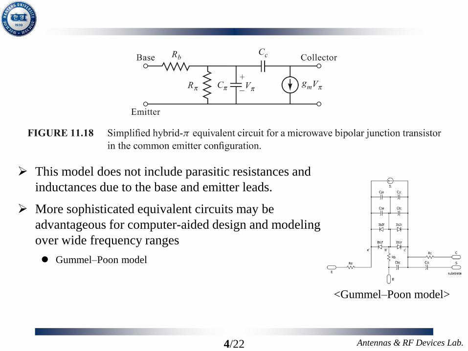
This model does not include parasitic resistances and
inductances due to the base and emitter leads.
More sophisticated equivalent circuits may be
advantageous for computer-aided design and modeling
over wide frequency ranges
Gummel–Poon model
<Gummel–Poon model>

5/22 Antennas & RF Devices Lab.
When the element values of the model are fairly constant over a range of
operating bias conditions, load conditions, and frequency, it is simpler to
treat the transistor as a two-port network, characterized by two-port
parameters.
In practice, scattering parameters, measured under typical operating
conditions, are usually used for this purpose and are supplied by the device
manufacturer.
Table 11.4 shows scattering parameters for a typical RF silicon junction
transistor in a common emitter configuration.

6/22 Antennas & RF Devices Lab.
The equivalent circuit of Figure 11.18 can be used to estimate the upper
frequency limit, fT , defined as the threshold frequency where the short-
circuit current gain of the transistor is unity.
If we assume an input current Iin at the base, the output short-circuit current at
the collector is Iout = gmVπ . (Vπ = Iin/jωCπ )
So the short-circuit current gain is
The current gain is seen to decrease with frequency, and is unity at the
threshold frequency,
gm : transconductance

7/22 Antennas & RF Devices Lab.
The biasing point for the transistor depends on the application and type of
device, with low collector currents generally giving the best noise figure, and
higher collector currents giving the best power gain.
FIGURE 11.19 (a) DC characteristics of an npn BJT; (b) biasing and decoupling circuit for an npn BJT

8/22 Antennas & RF Devices Lab.
Heterojunction Bipolar Transistor
The operation of a heterojunction bipolar transistor (HBT) is essentially the
same as that of a BJT.
But an HBT has a base-emitter junction made from a compound
semiconductor material such as GaAs, indium phosphide (InP), or silicon
germanium (SiGe), often in conjunction with thin layers of other materials
(e.g., aluminum).
This structure offers much improved performance at high frequencies. Some
HBTs can operate at frequencies exceeding 100 GHz, and recent
developments with HBTs using SiGe have demonstrated that these devices
are useful in low-cost circuits operating at frequencies of 60 GHz or higher.

9/22 Antennas & RF Devices Lab.
Table 11.5 gives the scattering parameters at several frequencies for a popular
microwave HBT. Observe that |S21| decreases much less rapidly with
frequency when compared with the BJT of Table 11.4.
High levels of monolithic integration are easy and inexpensive with SiGe
HBTs, so this technology is proving to be very useful for low-cost millimeter
wave circuits for both defense and commercial applications.

10/22 Antennas & RF Devices Lab.
11.3 FIELD EFFECT TRANSISTORS
In contrast to BJTs, field effect transistors (FETs) are monopolar, with only
one carrier type (holes or electrons) providing current flow through the
device: n-channel FETs employ electrons, while p-channel devices use holes.
In addition, while a BJT is a current controlled device, an FET is a voltage-
controlled device, having a source-to-drain characteristic that is similar to that
of a voltage-dependent variable resistor.

11/22 Antennas & RF Devices Lab.
Metal Semiconductor Field Effect Transistor
One of the most important developments in microwave technology has been
the GaAs metal semiconductor field effect transistor (MESFET), as this
device permitted the first practical solid-state implementation of amplifiers,
oscillators, and mixers at microwave frequencies, leading to key applications
in radar, GPS, remote sensing, and wireless communications.
GaAs MESFETs can be used at frequencies well into the millimeter wave
range, with high gain and low noise figure, often making them the device of
choice for hybrid and monolithic integrated circuits at frequencies above
10 GHz.

12/22 Antennas & RF Devices Lab.
Figure 11.20 shows the cross section of a typical n-channel GaAs MESFET.
The gate junction is formed as a Schottky barrier. The desirable gain and
noise features of this transistor are a result of the higher electron mobility of
GaAs compared to silicon, and the absence of shot noise.
The device is biased with a drain-to-source voltage, Vds , and a gate-to-source
voltage, Vgs.
The maximum frequency of operation is limited by the gate length; present
FETs have gate lengths on the order of 0.2–0.6 µm, with corresponding upper
frequency limits of 100 to 50 GHz.

13/22 Antennas & RF Devices Lab.
A small-signal equivalent circuit for a microwave MESFET is shown in
Figure 11.21 for a common-source configuration.
The scattering parameters for a typical GaAs MESFET are given in Table
11.7.

14/22 Antennas & RF Devices Lab.
As we did for the BJT, we can use the equivalent circuit model of Figure
11.21 to determine the upper frequency of operation for a MESFET. For a
FET, the short-circuit current gain, 𝐺𝐼𝑠𝑐, is defined as the ratio of drain current
to gate current when the output is short circuited. For the unilateral case,
where Cgd = 0, the short circuit current gain is
The upper frequency threshold, fT , where the short-circuit current gain is
unity, is then given by
a result that is equivalent to (11.23) for a bipolar junction transistor.
(11.24) (11.23)

15/22 Antennas & RF Devices Lab.
For proper operation, the transistor must be biased at an appropriate operating
point. This depends on the application (low noise, high gain, high power), the
class of the amplifier (class A, class AB, class B), and the transistor.

16/22 Antennas & RF Devices Lab.
Metal Oxide Semiconductor Field Effect Transistor
The silicon metal oxide semiconductor field effect transistor (MOSFET) is the
most common type of FET, being used extensively in analog and digital
integrated circuits. Figure 11.23 shows a cross section of an n-channel
MOSFET.
MOSFETs can be used at frequencies into the UHF range, and can provide
powers of several hundred watts when devices are packaged in parallel.
Laterally diffused MOSFETs (LDMOS) have direct grounding of the
source, and can operate at low microwave frequencies with high powers.
These devices are commonly used for high-power transmitters for cellular
base stations at 900 and 1900 MHz.

17/22 Antennas & RF Devices Lab.
High-density integrated circuits typically use complementary MOS (CMOS),
where both n-channel and p-channel devices are used. This technology is very
mature, and has the advantages of low power requirements and low unit cost.
Most RF and microwave MOSFETs use n-channel silicon devices, although
GaN devices are possible.
<CMOS Transceiver>

18/22 Antennas & RF Devices Lab.
High Electron Mobility Transistor
The high electron mobility transistor (HEMT) is a heterojunction FET,
meaning that it does not use a single semiconductor material, but instead is
constructed with several layers of compound semiconductor materials.
These may include transitions between gallium aluminum arsenide (GaAlAs),
GaAs, gallium indium arsenide (GaInAs), and similar compounds. These
structures result in high carrier mobility—about twice that found in a
standard MESFET. GaAs HEMTs can operate at frequencies above 100 GHz.

19/22 Antennas & RF Devices Lab.
Figure 11.24 shows the cross section of a HEMT device. It consists of semi-
insulating GaAs substrate, followed by an undoped GaAs layer, and then a
very thin undoped GaAlAs layer. This is topped with an n-doped GaAlAs
layer.
Several variations on this device are possible, including the use of different
compound semiconductors, and the pseudomorphic HEMT, which uses a
lattice mismatch between the layers. The relatively complicated structure of
the HEMT requires sophisticated fabrication techniques, leading to a
relatively high cost.

20/22 Antennas & RF Devices Lab.
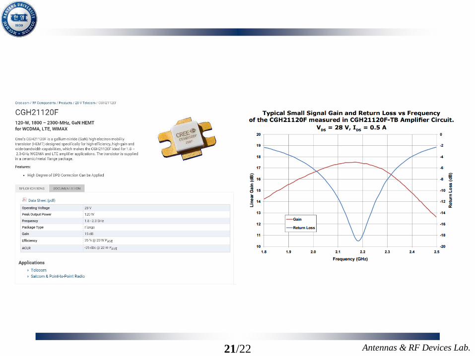
A relatively new type of HEMT uses GaN and aluminum gallium nitride
(AlGaN) on a silicon or SiC substrate. GaN HEMTs operate with drain
voltages in the range of 20–40 V, and can deliver powers up to 100 W at
frequencies in the low microwave range, making these devices popular for
high-power transmitters.
Table 11.8 gives the scattering parameters for a medium power GaN HEMT.
21/22 Antennas & RF Devices Lab.

22/22 Antennas & RF Devices Lab.
Thank you