Microstepping motor controller with motion engine and SPI · Microstepping motor controller with...
75
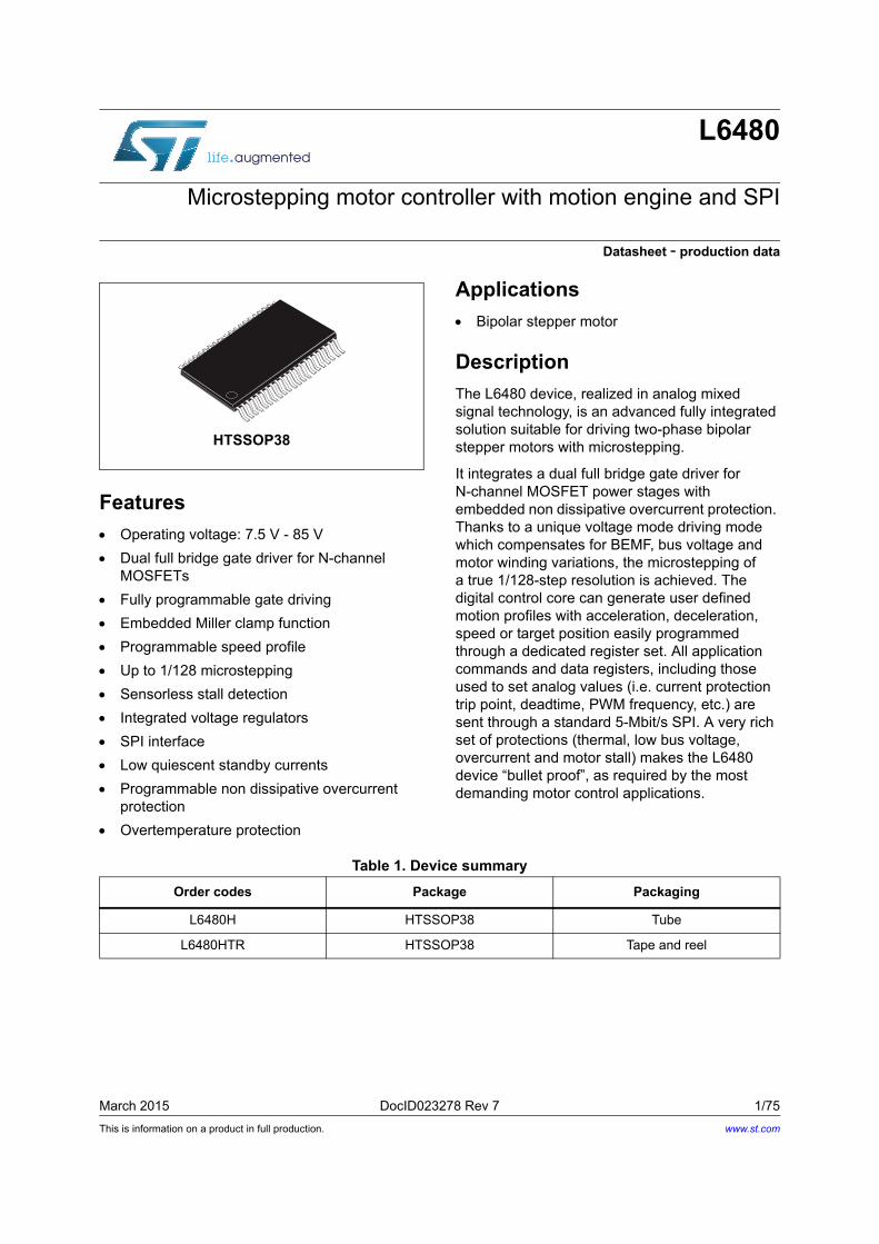
This is information on a product in full production. March 2015 DocID023278 Rev 7 1/75 L6480 Microstepping motor controller with motion engine and SPI Datasheet - production data Features Operating voltage: 7.5 V - 85 V Dual full bridge gate driver for N-channel MOSFETs Fully programmable gate driving Embedded Miller clamp function Programmable speed profile Up to 1/128 microstepping Sensorless stall detection Integrated voltage regulators SPI interface Low quiescent standby currents Programmable non dissipative overcurrent protection Overtemperature protection Applications Bipolar stepper motor Description The L6480 device, realized in analog mixed signal technology, is an advanced fully integrated solution suitable for driving two-phase bipolar stepper motors with microstepping. It integrates a dual full bridge gate driver for N-channel MOSFET power stages with embedded non dissipative overcurrent protection. Thanks to a unique voltage mode driving mode which compensates for BEMF, bus voltage and motor winding variations, the microstepping of a true 1/128-step resolution is achieved. The digital control core can generate user defined motion profiles with acceleration, deceleration, speed or target position easily programmed through a dedicated register set. All application commands and data registers, including those used to set analog values (i.e. current protection trip point, deadtime, PWM frequency, etc.) are sent through a standard 5-Mbit/s SPI. A very rich set of protections (thermal, low bus voltage, overcurrent and motor stall) makes the L6480 device “bullet proof”, as required by the most demanding motor control applications. HTSSOP38 Table 1. Device summary Order codes Package Packaging L6480H HTSSOP38 Tube L6480HTR HTSSOP38 Tape and reel www.st.com
Transcript of Microstepping motor controller with motion engine and SPI · Microstepping motor controller with...
This is information on a product in full production.
March 2015 DocID023278 Rev 7 1/75
L6480
Microstepping motor controller with motion engine and SPI
Datasheet - production data
Features
Operating voltage: 7.5 V - 85 V
Dual full bridge gate driver for N-channel MOSFETs
Fully programmable gate driving
Embedded Miller clamp function
Programmable speed profile
Up to 1/128 microstepping
Sensorless stall detection
Integrated voltage regulators
SPI interface
Low quiescent standby currents
Programmable non dissipative overcurrent protection
Overtemperature protection
Applications
Bipolar stepper motor
Description
The L6480 device, realized in analog mixed signal technology, is an advanced fully integrated solution suitable for driving two-phase bipolar stepper motors with microstepping.
It integrates a dual full bridge gate driver for N-channel MOSFET power stages with embedded non dissipative overcurrent protection. Thanks to a unique voltage mode driving mode which compensates for BEMF, bus voltage and motor winding variations, the microstepping of a true 1/128-step resolution is achieved. The digital control core can generate user defined motion profiles with acceleration, deceleration, speed or target position easily programmed through a dedicated register set. All application commands and data registers, including those used to set analog values (i.e. current protection trip point, deadtime, PWM frequency, etc.) are sent through a standard 5-Mbit/s SPI. A very rich set of protections (thermal, low bus voltage, overcurrent and motor stall) makes the L6480 device “bullet proof”, as required by the most demanding motor control applications.
HTSSOP38
Table 1. Device summary
Order codes Package Packaging
L6480H HTSSOP38 Tube
L6480HTR HTSSOP38 Tape and reel
www.st.com
Contents L6480
2/75 DocID023278 Rev 7
Contents
1 Block diagram . . . . . . . . . . . . . . . . . . . . . . . . . . . . . . . . . . . . . . . . . . . . . . 9
2 Electrical data . . . . . . . . . . . . . . . . . . . . . . . . . . . . . . . . . . . . . . . . . . . . . 10
2.1 Absolute maximum ratings . . . . . . . . . . . . . . . . . . . . . . . . . . . . . . . . . . . . 10
2.2 Recommended operating conditions . . . . . . . . . . . . . . . . . . . . . . . . . . . . .11
2.3 Thermal data . . . . . . . . . . . . . . . . . . . . . . . . . . . . . . . . . . . . . . . . . . . . . . .11
3 Electrical characteristics . . . . . . . . . . . . . . . . . . . . . . . . . . . . . . . . . . . . 12
4 Pin connection . . . . . . . . . . . . . . . . . . . . . . . . . . . . . . . . . . . . . . . . . . . . . 17
Pin list . . . . . . . . . . . . . . . . . . . . . . . . . . . . . . . . . . . . . . . . . . . . . . . . . . . . . . . . . . 17
5 Typical applications . . . . . . . . . . . . . . . . . . . . . . . . . . . . . . . . . . . . . . . . 19
6 Functional description . . . . . . . . . . . . . . . . . . . . . . . . . . . . . . . . . . . . . . 20
6.1 Device power-up . . . . . . . . . . . . . . . . . . . . . . . . . . . . . . . . . . . . . . . . . . . 20
6.2 Logic I/O . . . . . . . . . . . . . . . . . . . . . . . . . . . . . . . . . . . . . . . . . . . . . . . . . . 20
6.3 Charge pump . . . . . . . . . . . . . . . . . . . . . . . . . . . . . . . . . . . . . . . . . . . . . . 20
6.4 Microstepping . . . . . . . . . . . . . . . . . . . . . . . . . . . . . . . . . . . . . . . . . . . . . . 21
Automatic Full-step and Boost modes . . . . . . . . . . . . . . . . . . . . . . . . . . . . . . . . . . 22
6.5 Absolute position counter . . . . . . . . . . . . . . . . . . . . . . . . . . . . . . . . . . . . . 23
6.6 Programmable speed profiles . . . . . . . . . . . . . . . . . . . . . . . . . . . . . . . . . 23
6.7 Motor control commands . . . . . . . . . . . . . . . . . . . . . . . . . . . . . . . . . . . . . 24
6.7.1 Constant speed commands . . . . . . . . . . . . . . . . . . . . . . . . . . . . . . . . . . 24
6.7.2 Positioning commands . . . . . . . . . . . . . . . . . . . . . . . . . . . . . . . . . . . . . . 24
6.7.3 Motion commands . . . . . . . . . . . . . . . . . . . . . . . . . . . . . . . . . . . . . . . . . 25
6.7.4 Stop commands . . . . . . . . . . . . . . . . . . . . . . . . . . . . . . . . . . . . . . . . . . . 26
6.7.5 Step-clock mode . . . . . . . . . . . . . . . . . . . . . . . . . . . . . . . . . . . . . . . . . . 26
6.7.6 GoUntil and ReleaseSW commands . . . . . . . . . . . . . . . . . . . . . . . . . . . 26
6.8 Internal oscillator and oscillator driver . . . . . . . . . . . . . . . . . . . . . . . . . . . 27
6.8.1 Internal oscillator . . . . . . . . . . . . . . . . . . . . . . . . . . . . . . . . . . . . . . . . . . 27
6.8.2 External clock source . . . . . . . . . . . . . . . . . . . . . . . . . . . . . . . . . . . . . . . 27
6.9 Overcurrent detection . . . . . . . . . . . . . . . . . . . . . . . . . . . . . . . . . . . . . . . . 29
DocID023278 Rev 7 3/75
L6480 Contents
75
6.10 Undervoltage lockout (UVLO) . . . . . . . . . . . . . . . . . . . . . . . . . . . . . . . . . 30
6.11 VS undervoltage lockout (UVLO_ADC) . . . . . . . . . . . . . . . . . . . . . . . . . . 30
6.12 Thermal warning and thermal shutdown . . . . . . . . . . . . . . . . . . . . . . . . . 30
6.13 Reset and standby . . . . . . . . . . . . . . . . . . . . . . . . . . . . . . . . . . . . . . . . . . 31
6.14 External switch (SW pin) . . . . . . . . . . . . . . . . . . . . . . . . . . . . . . . . . . . . . 31
6.15 Programmable gate drivers . . . . . . . . . . . . . . . . . . . . . . . . . . . . . . . . . . . 32
6.16 Deadtime and blanking time . . . . . . . . . . . . . . . . . . . . . . . . . . . . . . . . . . . 33
6.17 Integrated analog to digital converter . . . . . . . . . . . . . . . . . . . . . . . . . . . . 33
6.18 Supply management and internal voltage regulators . . . . . . . . . . . . . . . . 34
6.19 BUSY/SYNC pin . . . . . . . . . . . . . . . . . . . . . . . . . . . . . . . . . . . . . . . . . . . . 35
6.20 FLAG pin . . . . . . . . . . . . . . . . . . . . . . . . . . . . . . . . . . . . . . . . . . . . . . . . . 35
7 Phase current control . . . . . . . . . . . . . . . . . . . . . . . . . . . . . . . . . . . . . . . 36
7.1 PWM sine wave generators . . . . . . . . . . . . . . . . . . . . . . . . . . . . . . . . . . . 36
7.2 Sensorless stall detection . . . . . . . . . . . . . . . . . . . . . . . . . . . . . . . . . . . . . 37
7.3 Low speed optimization . . . . . . . . . . . . . . . . . . . . . . . . . . . . . . . . . . . . . . 37
7.4 BEMF compensation . . . . . . . . . . . . . . . . . . . . . . . . . . . . . . . . . . . . . . . . 38
7.5 Motor supply voltage compensation . . . . . . . . . . . . . . . . . . . . . . . . . . . . . 39
7.6 Winding resistance thermal drift compensation . . . . . . . . . . . . . . . . . . . . 40
8 Serial interface . . . . . . . . . . . . . . . . . . . . . . . . . . . . . . . . . . . . . . . . . . . . . 41
9 Programming manual . . . . . . . . . . . . . . . . . . . . . . . . . . . . . . . . . . . . . . . 43
9.1 Register and flag description . . . . . . . . . . . . . . . . . . . . . . . . . . . . . . . . . . 43
9.1.1 ABS_POS . . . . . . . . . . . . . . . . . . . . . . . . . . . . . . . . . . . . . . . . . . . . . . . 44
9.1.2 EL_POS . . . . . . . . . . . . . . . . . . . . . . . . . . . . . . . . . . . . . . . . . . . . . . . . . 44
9.1.3 MARK . . . . . . . . . . . . . . . . . . . . . . . . . . . . . . . . . . . . . . . . . . . . . . . . . . 45
9.1.4 SPEED . . . . . . . . . . . . . . . . . . . . . . . . . . . . . . . . . . . . . . . . . . . . . . . . . . 45
9.1.5 ACC . . . . . . . . . . . . . . . . . . . . . . . . . . . . . . . . . . . . . . . . . . . . . . . . . . . . 45
9.1.6 DEC . . . . . . . . . . . . . . . . . . . . . . . . . . . . . . . . . . . . . . . . . . . . . . . . . . . . 46
9.1.7 MAX_SPEED . . . . . . . . . . . . . . . . . . . . . . . . . . . . . . . . . . . . . . . . . . . . . 46
9.1.8 MIN_SPEED . . . . . . . . . . . . . . . . . . . . . . . . . . . . . . . . . . . . . . . . . . . . . 46
9.1.9 FS_SPD . . . . . . . . . . . . . . . . . . . . . . . . . . . . . . . . . . . . . . . . . . . . . . . . . 47
9.1.10 KVAL_HOLD, KVAL_RUN, KVAL_ACC and KVAL_DEC . . . . . . . . . . . 47
9.1.11 INT_SPEED . . . . . . . . . . . . . . . . . . . . . . . . . . . . . . . . . . . . . . . . . . . . . . 48
Contents L6480
4/75 DocID023278 Rev 7
9.1.12 ST_SLP . . . . . . . . . . . . . . . . . . . . . . . . . . . . . . . . . . . . . . . . . . . . . . . . . 48
9.1.13 FN_SLP_ACC . . . . . . . . . . . . . . . . . . . . . . . . . . . . . . . . . . . . . . . . . . . . 48
9.1.14 FN_SLP_DEC . . . . . . . . . . . . . . . . . . . . . . . . . . . . . . . . . . . . . . . . . . . . 49
9.1.15 K_THERM . . . . . . . . . . . . . . . . . . . . . . . . . . . . . . . . . . . . . . . . . . . . . . . 49
9.1.16 ADC_OUT . . . . . . . . . . . . . . . . . . . . . . . . . . . . . . . . . . . . . . . . . . . . . . . 49
9.1.17 OCD_TH . . . . . . . . . . . . . . . . . . . . . . . . . . . . . . . . . . . . . . . . . . . . . . . . 50
9.1.18 STALL_TH . . . . . . . . . . . . . . . . . . . . . . . . . . . . . . . . . . . . . . . . . . . . . . . 50
9.1.19 STEP_MODE . . . . . . . . . . . . . . . . . . . . . . . . . . . . . . . . . . . . . . . . . . . . . 50
9.1.20 ALARM_EN . . . . . . . . . . . . . . . . . . . . . . . . . . . . . . . . . . . . . . . . . . . . . . 52
9.1.21 GATECFG1 . . . . . . . . . . . . . . . . . . . . . . . . . . . . . . . . . . . . . . . . . . . . . . 52
9.1.22 GATECFG2 . . . . . . . . . . . . . . . . . . . . . . . . . . . . . . . . . . . . . . . . . . . . . . 53
9.1.23 CONFIG . . . . . . . . . . . . . . . . . . . . . . . . . . . . . . . . . . . . . . . . . . . . . . . . . 54
9.1.24 STATUS . . . . . . . . . . . . . . . . . . . . . . . . . . . . . . . . . . . . . . . . . . . . . . . . . 59
9.2 Application commands . . . . . . . . . . . . . . . . . . . . . . . . . . . . . . . . . . . . . . . 62
9.2.1 Command management . . . . . . . . . . . . . . . . . . . . . . . . . . . . . . . . . . . . 63
9.2.2 Nop . . . . . . . . . . . . . . . . . . . . . . . . . . . . . . . . . . . . . . . . . . . . . . . . . . . . 64
9.2.3 SetParam (PARAM, VALUE) . . . . . . . . . . . . . . . . . . . . . . . . . . . . . . . . . 64
9.2.4 GetParam (PARAM) . . . . . . . . . . . . . . . . . . . . . . . . . . . . . . . . . . . . . . . 64
9.2.5 Run (DIR, SPD) . . . . . . . . . . . . . . . . . . . . . . . . . . . . . . . . . . . . . . . . . . . 65
9.2.6 StepClock (DIR) . . . . . . . . . . . . . . . . . . . . . . . . . . . . . . . . . . . . . . . . . . . 65
9.2.7 Move (DIR, N_STEP) . . . . . . . . . . . . . . . . . . . . . . . . . . . . . . . . . . . . . . 66
9.2.8 GoTo (ABS_POS) . . . . . . . . . . . . . . . . . . . . . . . . . . . . . . . . . . . . . . . . . 66
9.2.9 GoTo_DIR (DIR, ABS_POS) . . . . . . . . . . . . . . . . . . . . . . . . . . . . . . . . . 67
9.2.10 GoUntil (ACT, DIR, SPD) . . . . . . . . . . . . . . . . . . . . . . . . . . . . . . . . . . . . 67
9.2.11 ReleaseSW (ACT, DIR) . . . . . . . . . . . . . . . . . . . . . . . . . . . . . . . . . . . . . 68
9.2.12 GoHome . . . . . . . . . . . . . . . . . . . . . . . . . . . . . . . . . . . . . . . . . . . . . . . . 68
9.2.13 GoMark . . . . . . . . . . . . . . . . . . . . . . . . . . . . . . . . . . . . . . . . . . . . . . . . . 68
9.2.14 ResetPos . . . . . . . . . . . . . . . . . . . . . . . . . . . . . . . . . . . . . . . . . . . . . . . . 69
9.2.15 ResetDevice . . . . . . . . . . . . . . . . . . . . . . . . . . . . . . . . . . . . . . . . . . . . . 69
9.2.16 SoftStop . . . . . . . . . . . . . . . . . . . . . . . . . . . . . . . . . . . . . . . . . . . . . . . . . 69
9.2.17 HardStop . . . . . . . . . . . . . . . . . . . . . . . . . . . . . . . . . . . . . . . . . . . . . . . . 70
9.2.18 SoftHiZ . . . . . . . . . . . . . . . . . . . . . . . . . . . . . . . . . . . . . . . . . . . . . . . . . . 70
9.2.19 HardHiZ . . . . . . . . . . . . . . . . . . . . . . . . . . . . . . . . . . . . . . . . . . . . . . . . . 70
9.2.20 GetStatus . . . . . . . . . . . . . . . . . . . . . . . . . . . . . . . . . . . . . . . . . . . . . . . . 71
DocID023278 Rev 7 5/75
L6480 Contents
75
10 Package information . . . . . . . . . . . . . . . . . . . . . . . . . . . . . . . . . . . . . . . . 72
HTSSOP38 package information . . . . . . . . . . . . . . . . . . . . . . . . . . . . . . . . . . . . . 72
11 Revision history . . . . . . . . . . . . . . . . . . . . . . . . . . . . . . . . . . . . . . . . . . . 74
List of tables L6480
6/75 DocID023278 Rev 7
List of tables
Table 1. Device summary . . . . . . . . . . . . . . . . . . . . . . . . . . . . . . . . . . . . . . . . . . . . . . . . . . . . . . . . . . 1Table 2. Absolute maximum ratings . . . . . . . . . . . . . . . . . . . . . . . . . . . . . . . . . . . . . . . . . . . . . . . . . 10Table 3. Recommended operating conditions . . . . . . . . . . . . . . . . . . . . . . . . . . . . . . . . . . . . . . . . . 11Table 4. Thermal data. . . . . . . . . . . . . . . . . . . . . . . . . . . . . . . . . . . . . . . . . . . . . . . . . . . . . . . . . . . . 11Table 5. Electrical characteristics . . . . . . . . . . . . . . . . . . . . . . . . . . . . . . . . . . . . . . . . . . . . . . . . . . . 12Table 6. Pin description . . . . . . . . . . . . . . . . . . . . . . . . . . . . . . . . . . . . . . . . . . . . . . . . . . . . . . . . . . 17Table 7. Typical application values. . . . . . . . . . . . . . . . . . . . . . . . . . . . . . . . . . . . . . . . . . . . . . . . . . 19Table 8. CL values according to external oscillator frequency . . . . . . . . . . . . . . . . . . . . . . . . . . . . . 28Table 9. UVLO thresholds . . . . . . . . . . . . . . . . . . . . . . . . . . . . . . . . . . . . . . . . . . . . . . . . . . . . . . . . 30Table 10. Thermal protection summarizing table . . . . . . . . . . . . . . . . . . . . . . . . . . . . . . . . . . . . . . . . 31Table 11. Register map . . . . . . . . . . . . . . . . . . . . . . . . . . . . . . . . . . . . . . . . . . . . . . . . . . . . . . . . . . . 43Table 12. EL_POS register . . . . . . . . . . . . . . . . . . . . . . . . . . . . . . . . . . . . . . . . . . . . . . . . . . . . . . . . . 44Table 13. MIN_SPEED register . . . . . . . . . . . . . . . . . . . . . . . . . . . . . . . . . . . . . . . . . . . . . . . . . . . . . 46Table 14. FS_SPD register . . . . . . . . . . . . . . . . . . . . . . . . . . . . . . . . . . . . . . . . . . . . . . . . . . . . . . . . . 47Table 15. Voltage amplitude regulation registers . . . . . . . . . . . . . . . . . . . . . . . . . . . . . . . . . . . . . . . . 48Table 16. Winding resistance thermal drift compensation coefficient . . . . . . . . . . . . . . . . . . . . . . . . . 49Table 17. ADC_OUT value and motor supply voltage compensation feature . . . . . . . . . . . . . . . . . . 49Table 18. Overcurrent detection threshold . . . . . . . . . . . . . . . . . . . . . . . . . . . . . . . . . . . . . . . . . . . . . 50Table 19. Stall detection threshold . . . . . . . . . . . . . . . . . . . . . . . . . . . . . . . . . . . . . . . . . . . . . . . . . . . 50Table 20. STEP_MODE register. . . . . . . . . . . . . . . . . . . . . . . . . . . . . . . . . . . . . . . . . . . . . . . . . . . . . 50Table 21. Step mode selection . . . . . . . . . . . . . . . . . . . . . . . . . . . . . . . . . . . . . . . . . . . . . . . . . . . . . . 51Table 22. SYNC signal source . . . . . . . . . . . . . . . . . . . . . . . . . . . . . . . . . . . . . . . . . . . . . . . . . . . . . . 51Table 23. ALARM_EN register . . . . . . . . . . . . . . . . . . . . . . . . . . . . . . . . . . . . . . . . . . . . . . . . . . . . . . 52Table 24. GATECFG1 register . . . . . . . . . . . . . . . . . . . . . . . . . . . . . . . . . . . . . . . . . . . . . . . . . . . . . . 52Table 25. IGATE parameter . . . . . . . . . . . . . . . . . . . . . . . . . . . . . . . . . . . . . . . . . . . . . . . . . . . . . . . . 52Table 26. TCC parameter . . . . . . . . . . . . . . . . . . . . . . . . . . . . . . . . . . . . . . . . . . . . . . . . . . . . . . . . . . 53Table 27. TBOOST parameter . . . . . . . . . . . . . . . . . . . . . . . . . . . . . . . . . . . . . . . . . . . . . . . . . . . . . . 53Table 28. GATECFG2 register (voltage mode) . . . . . . . . . . . . . . . . . . . . . . . . . . . . . . . . . . . . . . . . . 53Table 29. TDT parameter . . . . . . . . . . . . . . . . . . . . . . . . . . . . . . . . . . . . . . . . . . . . . . . . . . . . . . . . . . 54Table 30. TBLANK parameter . . . . . . . . . . . . . . . . . . . . . . . . . . . . . . . . . . . . . . . . . . . . . . . . . . . . . . 54Table 31. CONFIG register . . . . . . . . . . . . . . . . . . . . . . . . . . . . . . . . . . . . . . . . . . . . . . . . . . . . . . . . . 54Table 32. Oscillator management . . . . . . . . . . . . . . . . . . . . . . . . . . . . . . . . . . . . . . . . . . . . . . . . . . . . 55Table 33. External switch hard stop interrupt mode . . . . . . . . . . . . . . . . . . . . . . . . . . . . . . . . . . . . . . 55Table 34. Overcurrent event . . . . . . . . . . . . . . . . . . . . . . . . . . . . . . . . . . . . . . . . . . . . . . . . . . . . . . . . 56Table 35. Programmable VCC regulator output voltage . . . . . . . . . . . . . . . . . . . . . . . . . . . . . . . . . . . . . . . 56Table 36. Programmable UVLO thresholds . . . . . . . . . . . . . . . . . . . . . . . . . . . . . . . . . . . . . . . . . . . . 56Table 37. Motor supply voltage compensation enable . . . . . . . . . . . . . . . . . . . . . . . . . . . . . . . . . . . . 56Table 38. PWM frequency: integer division factor . . . . . . . . . . . . . . . . . . . . . . . . . . . . . . . . . . . . . . . 57Table 39. PWM frequency: multiplication factor . . . . . . . . . . . . . . . . . . . . . . . . . . . . . . . . . . . . . . . . . 57Table 40. Available PWM frequencies [kHz]: 8-MHz oscillator frequency . . . . . . . . . . . . . . . . . . . . . 58Table 41. Available PWM frequencies [kHz]: 16-MHz oscillator frequency . . . . . . . . . . . . . . . . . . . . 58Table 42. Available PWM frequencies [kHz]: 24-MHz oscillator frequency . . . . . . . . . . . . . . . . . . . . 59Table 43. Available PWM frequencies [kHz]: 32-MHz oscillator frequency . . . . . . . . . . . . . . . . . . . . 59Table 44. STATUS register. . . . . . . . . . . . . . . . . . . . . . . . . . . . . . . . . . . . . . . . . . . . . . . . . . . . . . . . . 59Table 45. STATUS register TH_STATUS bits . . . . . . . . . . . . . . . . . . . . . . . . . . . . . . . . . . . . . . . . . . 60Table 46. STATUS register DIR bit. . . . . . . . . . . . . . . . . . . . . . . . . . . . . . . . . . . . . . . . . . . . . . . . . . . 60Table 47. STATUS register MOT_STATUS bits . . . . . . . . . . . . . . . . . . . . . . . . . . . . . . . . . . . . . . . . . 61Table 48. Application commands . . . . . . . . . . . . . . . . . . . . . . . . . . . . . . . . . . . . . . . . . . . . . . . . . . . . 62
DocID023278 Rev 7 7/75
L6480 List of tables
75
Table 49. Nop command structure . . . . . . . . . . . . . . . . . . . . . . . . . . . . . . . . . . . . . . . . . . . . . . . . . . . 64Table 50. SetParam command structure . . . . . . . . . . . . . . . . . . . . . . . . . . . . . . . . . . . . . . . . . . . . . . 64Table 51. GetParam command structure . . . . . . . . . . . . . . . . . . . . . . . . . . . . . . . . . . . . . . . . . . . . . . 64Table 52. Run command structure . . . . . . . . . . . . . . . . . . . . . . . . . . . . . . . . . . . . . . . . . . . . . . . . . . . 65Table 53. StepClock command structure . . . . . . . . . . . . . . . . . . . . . . . . . . . . . . . . . . . . . . . . . . . . . . 65Table 54. Move command structure . . . . . . . . . . . . . . . . . . . . . . . . . . . . . . . . . . . . . . . . . . . . . . . . . . 66Table 55. GoTo command structure . . . . . . . . . . . . . . . . . . . . . . . . . . . . . . . . . . . . . . . . . . . . . . . . . . 66Table 56. GoTo_DIR command structure. . . . . . . . . . . . . . . . . . . . . . . . . . . . . . . . . . . . . . . . . . . . . . 67Table 57. GoUntil command structure . . . . . . . . . . . . . . . . . . . . . . . . . . . . . . . . . . . . . . . . . . . . . . . . 67Table 58. ReleaseSW command structure . . . . . . . . . . . . . . . . . . . . . . . . . . . . . . . . . . . . . . . . . . . . . 68Table 59. GoHome command structure . . . . . . . . . . . . . . . . . . . . . . . . . . . . . . . . . . . . . . . . . . . . . . . 68Table 60. GoMark command structure . . . . . . . . . . . . . . . . . . . . . . . . . . . . . . . . . . . . . . . . . . . . . . . . 68Table 61. ResetPos command structure . . . . . . . . . . . . . . . . . . . . . . . . . . . . . . . . . . . . . . . . . . . . . . 69Table 62. ResetDevice command structure . . . . . . . . . . . . . . . . . . . . . . . . . . . . . . . . . . . . . . . . . . . . 69Table 63. SoftStop command structure . . . . . . . . . . . . . . . . . . . . . . . . . . . . . . . . . . . . . . . . . . . . . . . 69Table 64. HardStop command structure. . . . . . . . . . . . . . . . . . . . . . . . . . . . . . . . . . . . . . . . . . . . . . . 70Table 65. SoftHiZ command structure . . . . . . . . . . . . . . . . . . . . . . . . . . . . . . . . . . . . . . . . . . . . . . . . 70Table 66. HardHiZ command structure. . . . . . . . . . . . . . . . . . . . . . . . . . . . . . . . . . . . . . . . . . . . . . . . 70Table 67. GetStatus command structure . . . . . . . . . . . . . . . . . . . . . . . . . . . . . . . . . . . . . . . . . . . . . . 71Table 68. HTSSOP38 mechanical data . . . . . . . . . . . . . . . . . . . . . . . . . . . . . . . . . . . . . . . . . . . . . . . 73Table 69. Document revision history . . . . . . . . . . . . . . . . . . . . . . . . . . . . . . . . . . . . . . . . . . . . . . . . . 74
List of figures L6480
8/75 DocID023278 Rev 7
List of figures
Figure 1. Block diagram . . . . . . . . . . . . . . . . . . . . . . . . . . . . . . . . . . . . . . . . . . . . . . . . . . . . . . . . . . . . 9Figure 2. Pin connection (top view) . . . . . . . . . . . . . . . . . . . . . . . . . . . . . . . . . . . . . . . . . . . . . . . . . . 17Figure 3. Typical application schematic . . . . . . . . . . . . . . . . . . . . . . . . . . . . . . . . . . . . . . . . . . . . . . . 19Figure 4. Charge pump circuitry. . . . . . . . . . . . . . . . . . . . . . . . . . . . . . . . . . . . . . . . . . . . . . . . . . . . . 21Figure 5. Normal mode and microstepping (128 microsteps) . . . . . . . . . . . . . . . . . . . . . . . . . . . . . . 21Figure 6. Automatic Full-step switching in Normal mode. . . . . . . . . . . . . . . . . . . . . . . . . . . . . . . . . . 22Figure 7. Automatic Full-step switching in Boost mode . . . . . . . . . . . . . . . . . . . . . . . . . . . . . . . . . . . 23Figure 8. Constant speed command examples . . . . . . . . . . . . . . . . . . . . . . . . . . . . . . . . . . . . . . . . . 24Figure 9. Positioning command examples . . . . . . . . . . . . . . . . . . . . . . . . . . . . . . . . . . . . . . . . . . . . . 25Figure 10. Motion command examples . . . . . . . . . . . . . . . . . . . . . . . . . . . . . . . . . . . . . . . . . . . . . . . . 25Figure 11. OSCIN and OSCOUT pin configuration . . . . . . . . . . . . . . . . . . . . . . . . . . . . . . . . . . . . . . . 28Figure 12. Overcurrent detection-principle scheme . . . . . . . . . . . . . . . . . . . . . . . . . . . . . . . . . . . . . . . 29Figure 13. External switch connection . . . . . . . . . . . . . . . . . . . . . . . . . . . . . . . . . . . . . . . . . . . . . . . . . 32Figure 14. Gate driving currents . . . . . . . . . . . . . . . . . . . . . . . . . . . . . . . . . . . . . . . . . . . . . . . . . . . . . 33Figure 15. Device supply pin management . . . . . . . . . . . . . . . . . . . . . . . . . . . . . . . . . . . . . . . . . . . . . 34Figure 16. Current distortion and compensation . . . . . . . . . . . . . . . . . . . . . . . . . . . . . . . . . . . . . . . . . 38Figure 17. BEMF compensation curve. . . . . . . . . . . . . . . . . . . . . . . . . . . . . . . . . . . . . . . . . . . . . . . . . 39Figure 18. Motor supply voltage compensation circuit . . . . . . . . . . . . . . . . . . . . . . . . . . . . . . . . . . . . . 39Figure 19. SPI timings diagram . . . . . . . . . . . . . . . . . . . . . . . . . . . . . . . . . . . . . . . . . . . . . . . . . . . . . . 41Figure 20. Daisy chain configuration . . . . . . . . . . . . . . . . . . . . . . . . . . . . . . . . . . . . . . . . . . . . . . . . . . 42Figure 21. Command with 3-byte argument . . . . . . . . . . . . . . . . . . . . . . . . . . . . . . . . . . . . . . . . . . . . 63Figure 22. Command with 3-byte response . . . . . . . . . . . . . . . . . . . . . . . . . . . . . . . . . . . . . . . . . . . . 63Figure 23. Command response aborted . . . . . . . . . . . . . . . . . . . . . . . . . . . . . . . . . . . . . . . . . . . . . . . 63Figure 24. HTSSOP38 package outline. . . . . . . . . . . . . . . . . . . . . . . . . . . . . . . . . . . . . . . . . . . . . . . . 72Figure 25. HTSSOP38 footprint . . . . . . . . . . . . . . . . . . . . . . . . . . . . . . . . . . . . . . . . . . . . . . . . . . . . . . 73
DocID023278 Rev 7 9/75
L6480 Block diagram
75
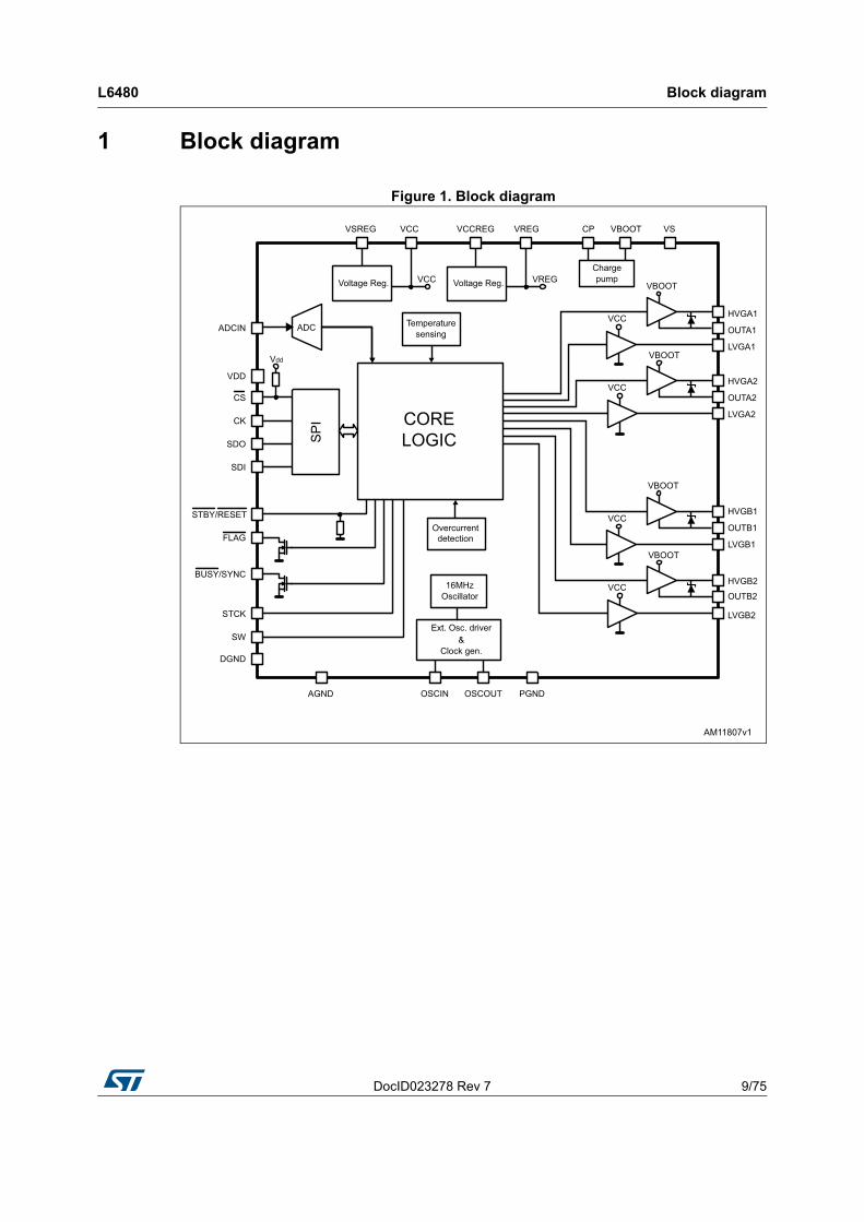
1 Block diagram
Figure 1. Block diagram
Electrical data L6480
10/75 DocID023278 Rev 7
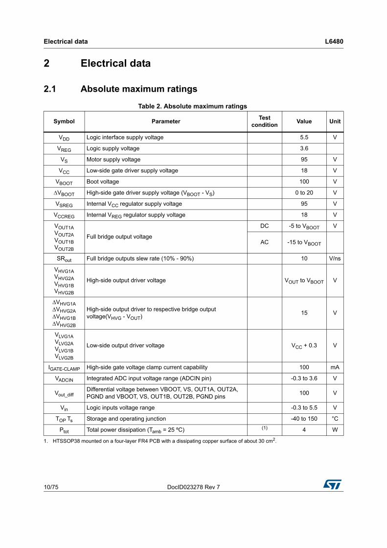
2 Electrical data
2.1 Absolute maximum ratings
Table 2. Absolute maximum ratings
Symbol ParameterTest
conditionValue Unit
VDD Logic interface supply voltage 5.5 V
VREG Logic supply voltage 3.6
VS Motor supply voltage 95 V
VCC Low-side gate driver supply voltage 18 V
VBOOT Boot voltage 100 V
VBOOT High-side gate driver supply voltage (VBOOT - VS) 0 to 20 V
VSREG Internal VCC regulator supply voltage 95 V
VCCREG Internal VREG regulator supply voltage 18 V
VOUT1A VOUT2A VOUT1B VOUT2B
Full bridge output voltage
DC -5 to VBOOT V
AC -15 to VBOOT
SRout Full bridge outputs slew rate (10% - 90%) 10 V/ns
VHVG1A VHVG2A VHVG1B VHVG2B
High-side output driver voltage VOUT to VBOOT V
VHVG1A VHVG2A VHVG1B VHVG2B
High-side output driver to respective bridge output voltage(VHVG - VOUT)
15 V
VLVG1A VLVG2A VLVG1B VLVG2B
Low-side output driver voltage VCC + 0.3 V
IGATE-CLAMP High-side gate voltage clamp current capability 100 mA
VADCIN Integrated ADC input voltage range (ADCIN pin) -0.3 to 3.6 V
Vout_diffDifferential voltage between VBOOT, VS, OUT1A, OUT2A, PGND and VBOOT, VS, OUT1B, OUT2B, PGND pins
100 V
Vin Logic inputs voltage range -0.3 to 5.5 V
TOP Ts Storage and operating junction -40 to 150 °C
Ptot Total power dissipation (Tamb = 25 ºC) (1) 4 W
1. HTSSOP38 mounted on a four-layer FR4 PCB with a dissipating copper surface of about 30 cm2.
DocID023278 Rev 7 11/75
L6480 Electrical data
75
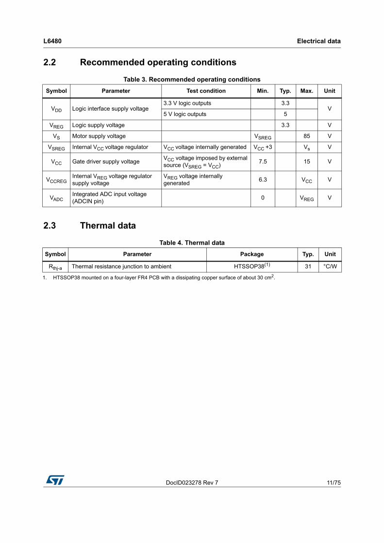
2.2 Recommended operating conditions
2.3 Thermal data
Table 3. Recommended operating conditions
Symbol Parameter Test condition Min. Typ. Max. Unit
VDD Logic interface supply voltage3.3 V logic outputs 3.3
V5 V logic outputs 5
VREG Logic supply voltage 3.3 V
VS Motor supply voltage VSREG 85 V
VSREG Internal VCC voltage regulator VCC voltage internally generated VCC +3 Vs V
VCC Gate driver supply voltageVCC voltage imposed by external source (VSREG = VCC)
7.5 15 V
VCCREGInternal VREG voltage regulator supply voltage
VREG voltage internally generated
6.3 VCC V
VADCIntegrated ADC input voltage (ADCIN pin)
0 VREG V
Table 4. Thermal data
Symbol Parameter Package Typ. Unit
Rthj-a Thermal resistance junction to ambient HTSSOP38(1) 31 °C/W
1. HTSSOP38 mounted on a four-layer FR4 PCB with a dissipating copper surface of about 30 cm2.
Electrical characteristics L6480
12/75 DocID023278 Rev 7
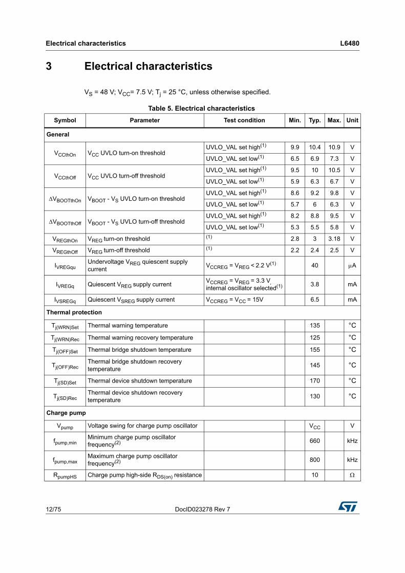
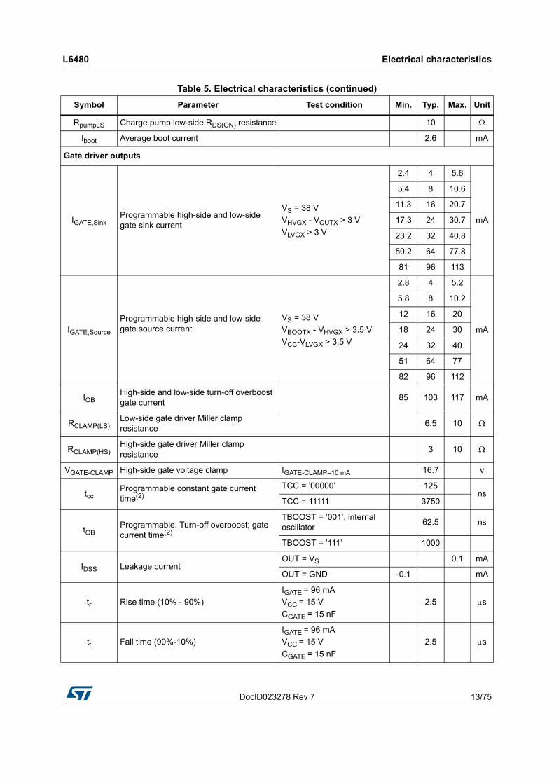
3 Electrical characteristics
VS = 48 V; VCC= 7.5 V; Tj = 25 °C, unless otherwise specified.
Table 5. Electrical characteristics
Symbol Parameter Test condition Min. Typ. Max. Unit
General
VCCthOn VCC UVLO turn-on thresholdUVLO_VAL set high(1) 9.9 10.4 10.9 V
UVLO_VAL set low(1) 6.5 6.9 7.3 V
VCCthOff VCC UVLO turn-off thresholdUVLO_VAL set high(1) 9.5 10 10.5 V
UVLO_VAL set low(1) 5.9 6.3 6.7 V
VBOOTthOn VBOOT - VS UVLO turn-on thresholdUVLO_VAL set high(1) 8.6 9.2 9.8 V
UVLO_VAL set low(1) 5.7 6 6.3 V
VBOOTthOff VBOOT - VS UVLO turn-off thresholdUVLO_VAL set high(1) 8.2 8.8 9.5 V
UVLO_VAL set low(1) 5.3 5.5 5.8 V
VREGthOn VREG turn-on threshold (1) 2.8 3 3.18 V
VREGthOff VREG turn-off threshold (1) 2.2 2.4 2.5 V
IVREGquUndervoltage VREG quiescent supply current
VCCREG = VREG < 2.2 V(1) 40 A
IVREGq Quiescent VREG supply currentVCCREG = VREG = 3.3 V, internal oscillator selected(1) 3.8 mA
IVSREGq Quiescent VSREG supply current VCCREG = VCC = 15V 6.5 mA
Thermal protection
Tj(WRN)Set Thermal warning temperature 135 °C
Tj(WRN)Rec Thermal warning recovery temperature 125 °C
Tj(OFF)Set Thermal bridge shutdown temperature 155 °C
Tj(OFF)RecThermal bridge shutdown recovery temperature
145 °C
Tj(SD)Set Thermal device shutdown temperature 170 °C
Tj(SD)RecThermal device shutdown recovery temperature
130 °C
Charge pump
Vpump Voltage swing for charge pump oscillator VCC V
fpump,minMinimum charge pump oscillator frequency(2) 660 kHz
fpump,maxMaximum charge pump oscillator frequency(2)
800 kHz
RpumpHS Charge pump high-side RDS(on) resistance 10
DocID023278 Rev 7 13/75
L6480 Electrical characteristics
75
RpumpLS Charge pump low-side RDS(ON) resistance 10
Iboot Average boot current 2.6 mA
Gate driver outputs
IGATE,SinkProgrammable high-side and low-side gate sink current
VS = 38 V
VHVGX - VOUTX > 3 V
VLVGX > 3 V
2.4 4 5.6
mA
5.4 8 10.6
11.3 16 20.7
17.3 24 30.7
23.2 32 40.8
50.2 64 77.8
81 96 113
IGATE,Source
Programmable high-side and low-side gate source current
VS = 38 V
VBOOTX - VHVGX > 3.5 V
VCC-VLVGX > 3.5 V
2.8 4 5.2
mA
5.8 8 10.2
12 16 20
18 24 30
24 32 40
51 64 77
82 96 112
IOBHigh-side and low-side turn-off overboost gate current
85 103 117 mA
RCLAMP(LS)Low-side gate driver Miller clamp resistance
6.5 10
RCLAMP(HS)High-side gate driver Miller clamp resistance
3 10
VGATE-CLAMP High-side gate voltage clamp IGATE-CLAMP=10 mA 16.7 v
tccProgrammable constant gate current time(2)
TCC = ’00000’ 125ns
TCC = 11111 3750
tOBProgrammable. Turn-off overboost; gate current time(2)
TBOOST = ’001’, internal oscillator
62.5 ns
TBOOST = ’111’ 1000
IDSS Leakage currentOUT = VS 0.1 mA
OUT = GND -0.1 mA
tr Rise time (10% - 90%)
IGATE = 96 mA
VCC = 15 V
CGATE = 15 nF
2.5 s
tf Fall time (90%-10%)
IGATE = 96 mA
VCC = 15 V
CGATE = 15 nF
2.5 s
Table 5. Electrical characteristics (continued)
Symbol Parameter Test condition Min. Typ. Max. Unit
Electrical characteristics L6480
14/75 DocID023278 Rev 7
SRgate Gate driver output slew rate
IGATE= 96 mA
VCC = 15 V
CGATE = 15 nF
6 V/s
Deadtime and blanking
tDT Programmable deadtime2 TDT = '00000' 125
nsTDT = ’11111’ 4000
tblank Programmable blanking time2 TBLANK = '000' 125
nsTBLANK = ’111’ 1000
Logic
VIL Low level logic input voltage 0.8 V
VIH High level logic input voltage 2 V
IIH High level logic input current VIN = 5 V, VDDIO = 5 V 1 µA
IIL Low level logic input current VIN = 0 V, VDDIO = 5 V -1 µA
VOL Low level logic output voltage(3)VDD = 3.3 V, IOL = 4 mA 0.3
VVDD = 5 V, IOL = 4 mA 0.3
VOH High level logic output voltageVDD = 3.3 V, IOH = 4 mA 2.4
VVDD = 5 V, IOH = 4 mA 4.7
RPUCS CS pull-up resistor 430
kRPDRST STBY/RESET pull-down resistor 450
RPUSW SW pull-up resistor 80
thigh,STCK Step-clock input high time 300 ns
tlow,STCK Step-clock input low time 300 ns
Internal oscillator and external oscillator driver
fosc,int Internal oscillator frequency Tj = 25 °C -5% 16 +5% MHz
fosc,extProgrammable external oscillator frequency
8 32 MHz
VOSCOUTH OSCOUT clock source high level voltage Internal oscillator 2.4 V
VOSCOUTL OSCOUT clock source low level voltage Internal oscillator 0.3 V
trOSCOUT
tfOSCOUTOSCOUT clock source rise and fall time Internal oscillator 10 ns
thigh OSCOUT clock source high time Internal oscillator 31.25 ns
textoscInternal to external oscillator switching delay
3 ms
tintoscExternal to internal oscillator switching delay
100 µs
Table 5. Electrical characteristics (continued)
Symbol Parameter Test condition Min. Typ. Max. Unit
DocID023278 Rev 7 15/75
L6480 Electrical characteristics
75
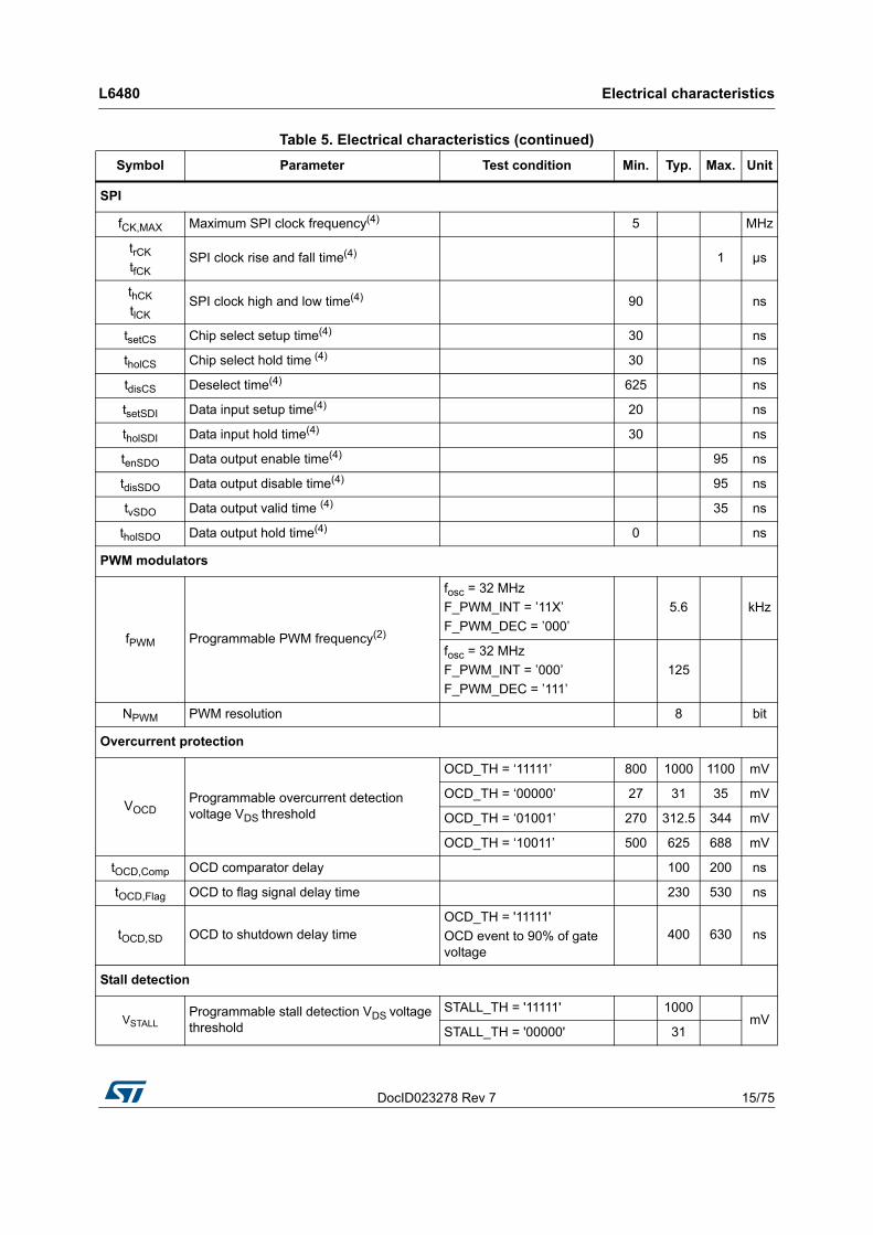
SPI
fCK,MAX Maximum SPI clock frequency(4) 5 MHz
trCK
tfCKSPI clock rise and fall time(4) 1 µs
thCK
tlCKSPI clock high and low time(4) 90 ns
tsetCS Chip select setup time(4) 30 ns
tholCS Chip select hold time (4) 30 ns
tdisCS Deselect time(4) 625 ns
tsetSDI Data input setup time(4) 20 ns
tholSDI Data input hold time(4) 30 ns
tenSDO Data output enable time(4) 95 ns
tdisSDO Data output disable time(4) 95 ns
tvSDO Data output valid time (4) 35 ns
tholSDO Data output hold time(4) 0 ns
PWM modulators
fPWM Programmable PWM frequency(2)
fosc = 32 MHz
F_PWM_INT = ’11X’
F_PWM_DEC = ’000’
5.6 kHz
fosc = 32 MHz
F_PWM_INT = ’000’
F_PWM_DEC = ’111’
125
NPWM PWM resolution 8 bit
Overcurrent protection
VOCDProgrammable overcurrent detection voltage VDS threshold
OCD_TH = ‘11111’ 800 1000 1100 mV
OCD_TH = ‘00000’ 27 31 35 mV
OCD_TH = ‘01001’ 270 312.5 344 mV
OCD_TH = ‘10011’ 500 625 688 mV
tOCD,Comp OCD comparator delay 100 200 ns
tOCD,Flag OCD to flag signal delay time 230 530 ns
tOCD,SD OCD to shutdown delay timeOCD_TH = '11111'
OCD event to 90% of gate voltage
400 630 ns
Stall detection
VSTALLProgrammable stall detection VDS voltage threshold
STALL_TH = '11111' 1000mV
STALL_TH = '00000' 31
Table 5. Electrical characteristics (continued)
Symbol Parameter Test condition Min. Typ. Max. Unit
Electrical characteristics L6480
16/75 DocID023278 Rev 7
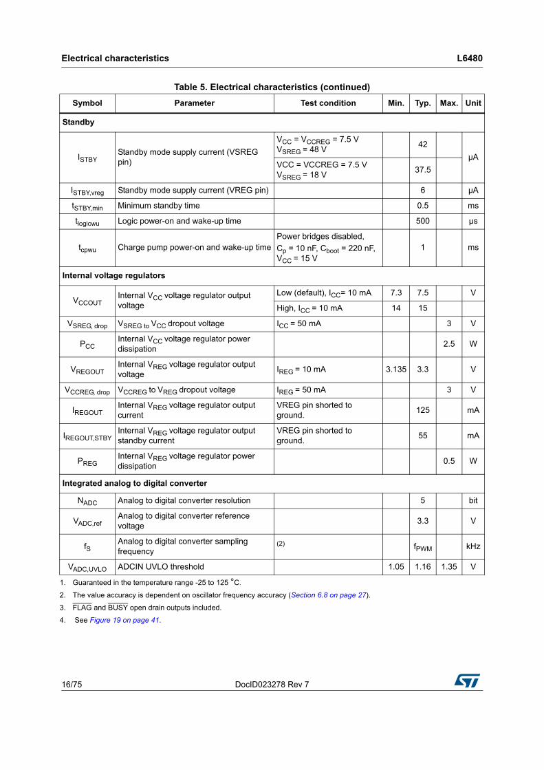
Standby
ISTBYStandby mode supply current (VSREG pin)
VCC = VCCREG = 7.5 V VSREG = 48 V
42
µAVCC = VCCREG = 7.5 V VSREG = 18 V
37.5
ISTBY,vreg Standby mode supply current (VREG pin) 6 µA
tSTBY,min Minimum standby time 0.5 ms
tlogicwu Logic power-on and wake-up time 500 µs
tcpwu Charge pump power-on and wake-up timePower bridges disabled,
Cp = 10 nF, Cboot = 220 nF, VCC = 15 V
1 ms
Internal voltage regulators
VCCOUTInternal VCC voltage regulator output voltage
Low (default), ICC= 10 mA 7.3 7.5 V
High, ICC = 10 mA 14 15
VSREG, drop VSREG to VCC dropout voltage ICC = 50 mA 3 V
PCCInternal VCC voltage regulator power dissipation
2.5 W
VREGOUTInternal VREG voltage regulator output voltage
IREG = 10 mA 3.135 3.3 V
VCCREG, drop VCCREG to VREG dropout voltage IREG = 50 mA 3 V
IREGOUTInternal VREG voltage regulator output current
VREG pin shorted to ground.
125 mA
IREGOUT,STBYInternal VREG voltage regulator output standby current
VREG pin shorted to ground.
55 mA
PREGInternal VREG voltage regulator power dissipation
0.5 W
Integrated analog to digital converter
NADC Analog to digital converter resolution 5 bit
VADC,refAnalog to digital converter reference voltage
3.3 V
fSAnalog to digital converter sampling frequency
(2) fPWM kHz
VADC,UVLO ADCIN UVLO threshold 1.05 1.16 1.35 V
1. Guaranteed in the temperature range -25 to 125 °C.
2. The value accuracy is dependent on oscillator frequency accuracy (Section 6.8 on page 27).
3. FLAG and BUSY open drain outputs included.
4. See Figure 19 on page 41.
Table 5. Electrical characteristics (continued)
Symbol Parameter Test condition Min. Typ. Max. Unit
DocID023278 Rev 7 17/75
L6480 Pin connection
75
4 Pin connection
Pin list
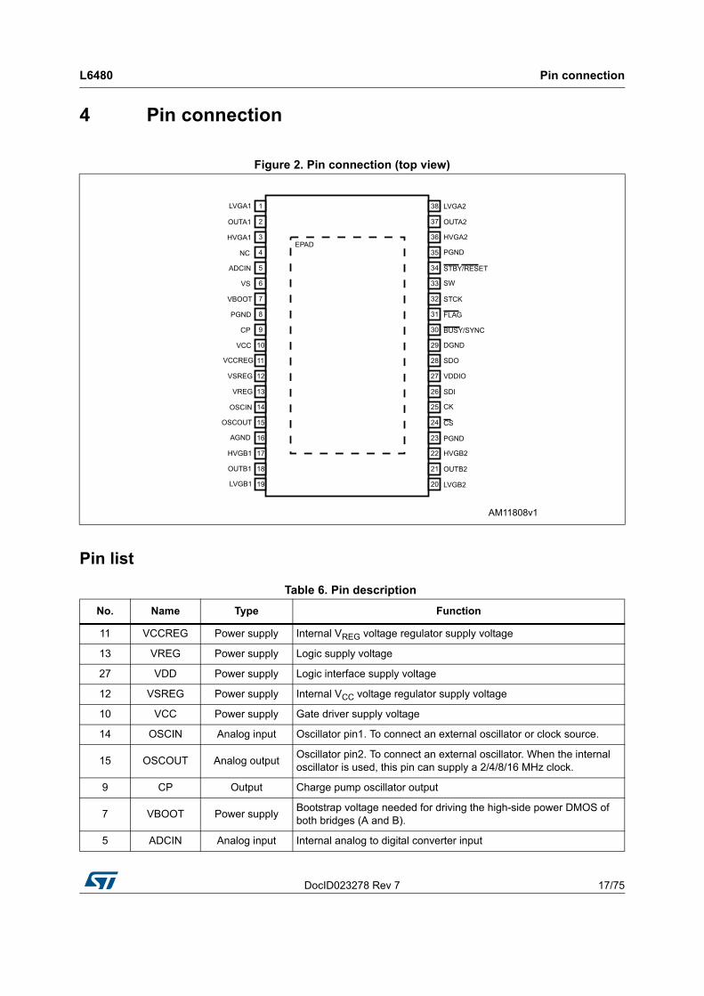
Figure 2. Pin connection (top view)
Table 6. Pin description
No. Name Type Function
11 VCCREG Power supply Internal VREG voltage regulator supply voltage
13 VREG Power supply Logic supply voltage
27 VDD Power supply Logic interface supply voltage
12 VSREG Power supply Internal VCC voltage regulator supply voltage
10 VCC Power supply Gate driver supply voltage
14 OSCIN Analog input Oscillator pin1. To connect an external oscillator or clock source.
15 OSCOUT Analog outputOscillator pin2. To connect an external oscillator. When the internal oscillator is used, this pin can supply a 2/4/8/16 MHz clock.
9 CP Output Charge pump oscillator output
7 VBOOT Power supplyBootstrap voltage needed for driving the high-side power DMOS of both bridges (A and B).
5 ADCIN Analog input Internal analog to digital converter input
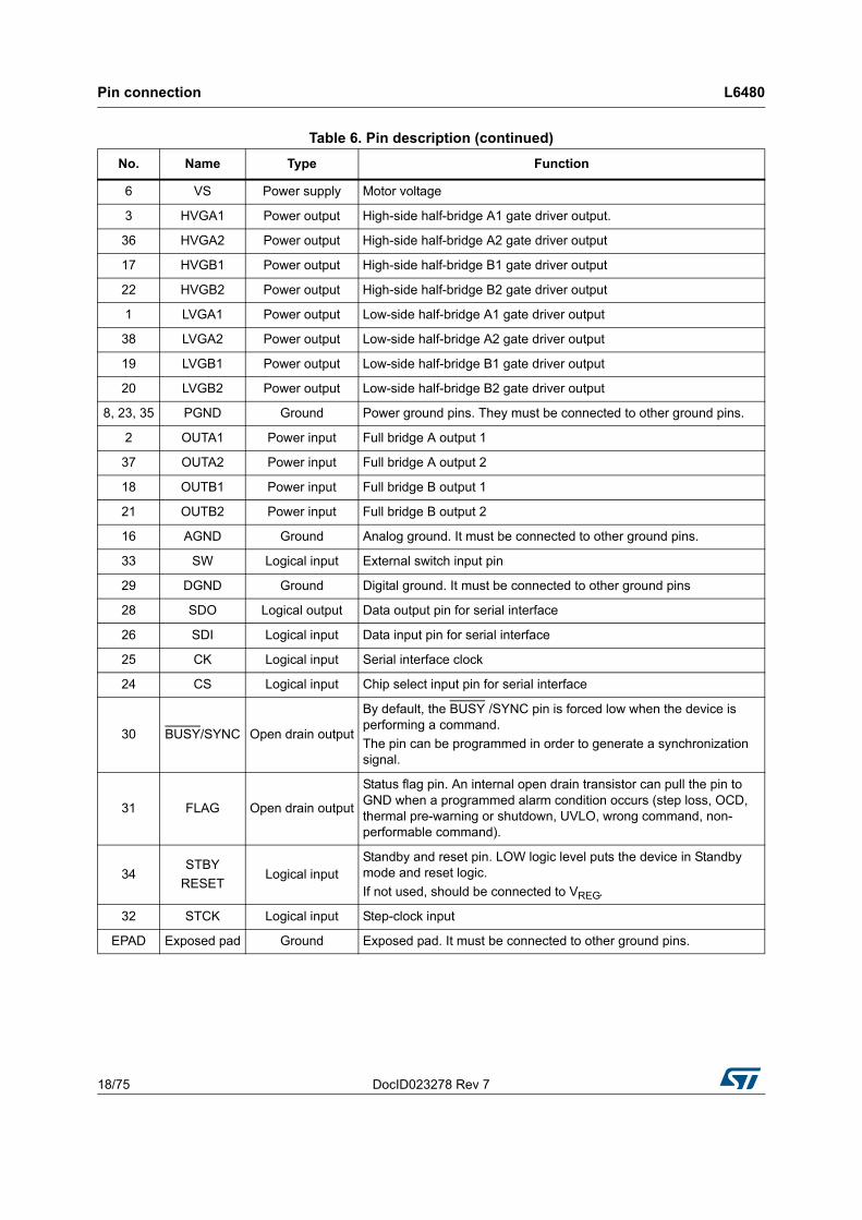
Pin connection L6480
18/75 DocID023278 Rev 7
6 VS Power supply Motor voltage
3 HVGA1 Power output High-side half-bridge A1 gate driver output.
36 HVGA2 Power output High-side half-bridge A2 gate driver output
17 HVGB1 Power output High-side half-bridge B1 gate driver output
22 HVGB2 Power output High-side half-bridge B2 gate driver output
1 LVGA1 Power output Low-side half-bridge A1 gate driver output
38 LVGA2 Power output Low-side half-bridge A2 gate driver output
19 LVGB1 Power output Low-side half-bridge B1 gate driver output
20 LVGB2 Power output Low-side half-bridge B2 gate driver output
8, 23, 35 PGND Ground Power ground pins. They must be connected to other ground pins.
2 OUTA1 Power input Full bridge A output 1
37 OUTA2 Power input Full bridge A output 2
18 OUTB1 Power input Full bridge B output 1
21 OUTB2 Power input Full bridge B output 2
16 AGND Ground Analog ground. It must be connected to other ground pins.
33 SW Logical input External switch input pin
29 DGND Ground Digital ground. It must be connected to other ground pins
28 SDO Logical output Data output pin for serial interface
26 SDI Logical input Data input pin for serial interface
25 CK Logical input Serial interface clock
24 CS Logical input Chip select input pin for serial interface
30 BUSY/SYNC Open drain output
By default, the BUSY /SYNC pin is forced low when the device is performing a command.
The pin can be programmed in order to generate a synchronization signal.
31 FLAG Open drain output
Status flag pin. An internal open drain transistor can pull the pin to GND when a programmed alarm condition occurs (step loss, OCD, thermal pre-warning or shutdown, UVLO, wrong command, non-performable command).
34STBY
RESETLogical input
Standby and reset pin. LOW logic level puts the device in Standby mode and reset logic.
If not used, should be connected to VREG.
32 STCK Logical input Step-clock input
EPAD Exposed pad Ground Exposed pad. It must be connected to other ground pins.
Table 6. Pin description (continued)
No. Name Type Function
DocID023278 Rev 7 19/75
L6480 Typical applications
75
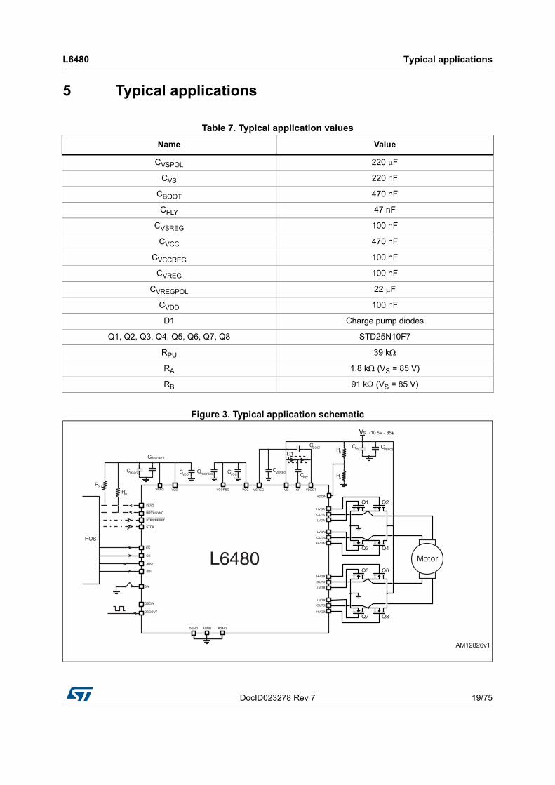
5 Typical applications
Figure 3. Typical application schematic
Table 7. Typical application values
Name Value
CVSPOL 220 µF
CVS 220 nF
CBOOT 470 nF
CFLY 47 nF
CVSREG 100 nF
CVCC 470 nF
CVCCREG 100 nF
CVREG 100 nF
CVREGPOL 22 µF
CVDD 100 nF
D1 Charge pump diodes
Q1, Q2, Q3, Q4, Q5, Q6, Q7, Q8 STD25N10F7
RPU 39 k
RA 1.8 k (VS = 85 V)
RB 91 k (VS = 85 V)
CK
SDO
SDI
SW
STCK
DGND
VDD
ADCIN
VCC CP VBOOT
PGND
VS
STBY/RESET
FLAG
CS
BUSY/SYNCHVGA1
LVGA1
LVGA2
HVGA2
HVGB1
LVGB1
OUTA1
OUTA2
OUTB1
LVGB2
HVGB2
OUTB2
AGND
VSREGVCCREG
OSCIN
OSCOUT
VREG
L6480
CFLY
CVS
CVCCCVCCREGCVDD
CVSREG
CBOOT CVSPOL
VS
CVREG
CVREGPOL
(10.5V - 85V)
D1
Q1 Q2
Q4Q3
Q5 Q6
Q8Q7
Motor
RB
RA
RPU
RPU
HOST
AM12826v1
Functional description L6480
20/75 DocID023278 Rev 7
6 Functional description
6.1 Device power-up
During power-up, the device is under reset (all logic IOs disabled and power bridges in high impedance state) until the following conditions are satisfied:
VREG is greater than VREGthOn
Internal oscillator is operative
STBY/RESET input is forced high.
After power-up, the device state is the following:
Parameters are set to default
Internal logic is driven by internal oscillator and a 2-MHz clock is provided by the OSCOUT pin
Bridges are disabled (high impedance).
FLAG output is forced low (UVLO failure indication).
After power-up, a period of tlogicwu must pass before applying a command to allow proper oscillator and logic startup.
Any movement command makes the device exit from High Z state (HardStop and SoftStop included).
6.2 Logic I/O
Pins CS, CK, SDI, STCK, SW and STBY/RESET are TTL/CMOS 3.3 V - 5 V compatible logic inputs.
Pin SDO is a TTL/CMOS compatible logic output. VDD pin voltage imposes logical output voltage range.
Pins FLAG and BUSY/SYNC are open drain outputs.
SW and CS inputs are internally pulled up to VDD and STBY/RESET input is internally pulled down to ground.
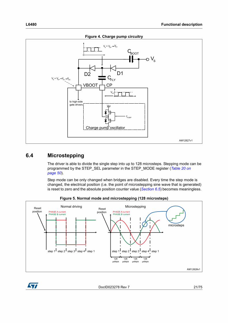
6.3 Charge pump
To ensure the correct driving of the high-side gate drivers, a voltage higher than the motor power supply voltage needs to be applied to the VBOOT pin. The high-side gate driver supply voltage VBOOT is obtained through an oscillator and a few external components realizing a charge pump (see Figure 4).
DocID023278 Rev 7 21/75
L6480 Functional description
75
Figure 4. Charge pump circuitry
6.4 Microstepping
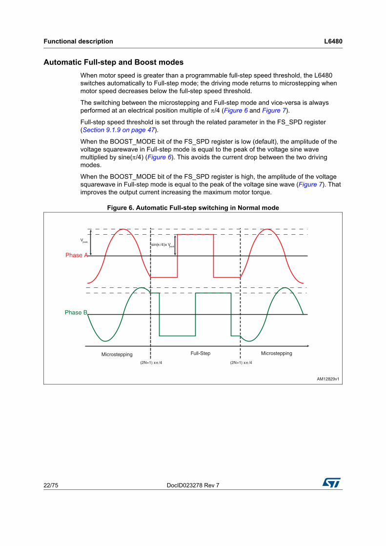
The driver is able to divide the single step into up to 128 microsteps. Stepping mode can be programmed by the STEP_SEL parameter in the STEP_MODE register (Table 20 on page 50).
Step mode can be only changed when bridges are disabled. Every time the step mode is changed, the electrical position (i.e. the point of microstepping sine wave that is generated) is reset to zero and the absolute position counter value (Section 6.5) becomes meaningless.
Figure 5. Normal mode and microstepping (128 microsteps)
Functional description L6480
22/75 DocID023278 Rev 7
Automatic Full-step and Boost modes
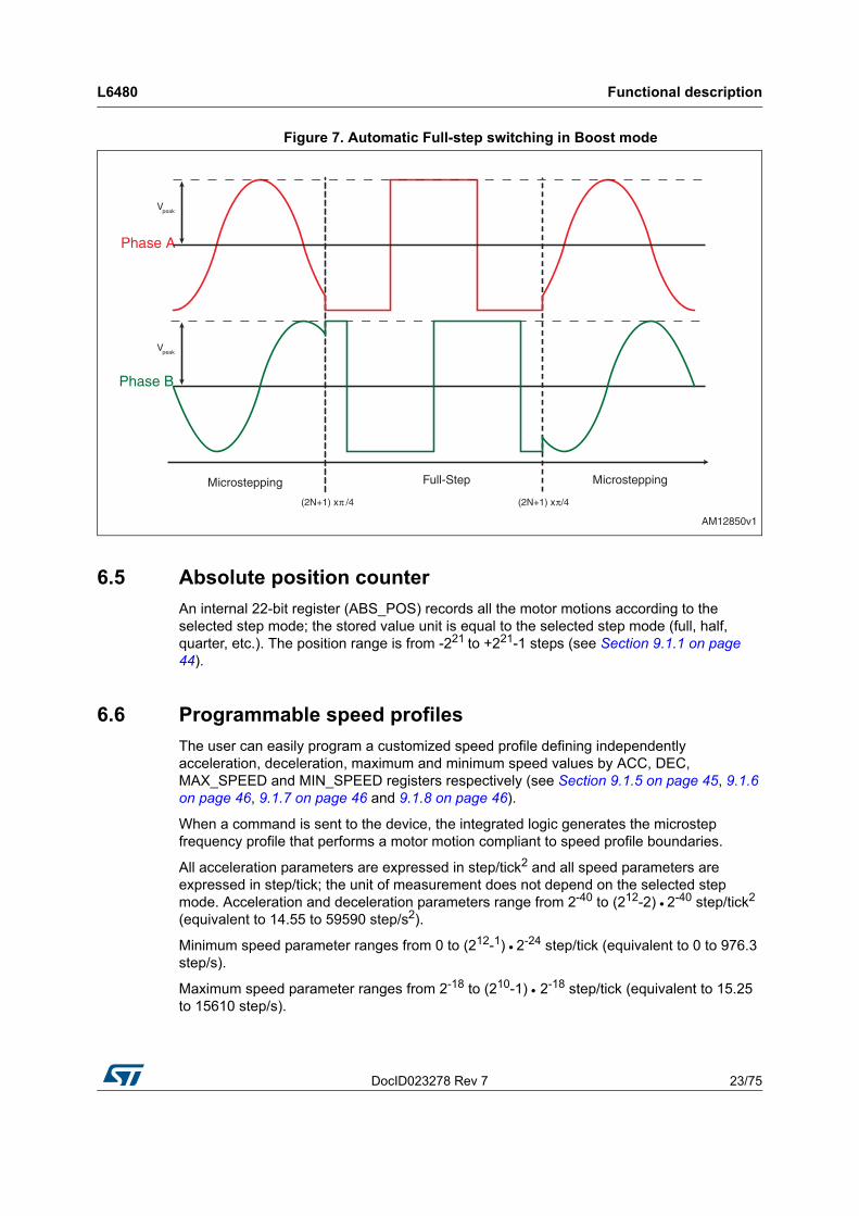
When motor speed is greater than a programmable full-step speed threshold, the L6480 switches automatically to Full-step mode; the driving mode returns to microstepping when motor speed decreases below the full-step speed threshold.
The switching between the microstepping and Full-step mode and vice-versa is always performed at an electrical position multiple of /4 (Figure 6 and Figure 7).
Full-step speed threshold is set through the related parameter in the FS_SPD register (Section 9.1.9 on page 47).
When the BOOST_MODE bit of the FS_SPD register is low (default), the amplitude of the voltage squarewave in Full-step mode is equal to the peak of the voltage sine wave multiplied by sine(/4) (Figure 6). This avoids the current drop between the two driving modes.
When the BOOST_MODE bit of the FS_SPD register is high, the amplitude of the voltage squarewave in Full-step mode is equal to the peak of the voltage sine wave (Figure 7). That improves the output current increasing the maximum motor torque.
Figure 6. Automatic Full-step switching in Normal mode
Phase A
Phase B
(2N+1) x π /4 (2N+1) x π /4
Full-StepMicrostepping Microstepping
Vpeaksin(π /4 )x Vpeak
AM12829v1
DocID023278 Rev 7 23/75
L6480 Functional description
75
Figure 7. Automatic Full-step switching in Boost mode
6.5 Absolute position counter
An internal 22-bit register (ABS_POS) records all the motor motions according to the selected step mode; the stored value unit is equal to the selected step mode (full, half, quarter, etc.). The position range is from -221 to +221-1 steps (see Section 9.1.1 on page 44).
6.6 Programmable speed profiles
The user can easily program a customized speed profile defining independently acceleration, deceleration, maximum and minimum speed values by ACC, DEC, MAX_SPEED and MIN_SPEED registers respectively (see Section 9.1.5 on page 45, 9.1.6 on page 46, 9.1.7 on page 46 and 9.1.8 on page 46).
When a command is sent to the device, the integrated logic generates the microstep frequency profile that performs a motor motion compliant to speed profile boundaries.
All acceleration parameters are expressed in step/tick2 and all speed parameters are expressed in step/tick; the unit of measurement does not depend on the selected step mode. Acceleration and deceleration parameters range from 2-40 to (212-2) 2-40 step/tick2 (equivalent to 14.55 to 59590 step/s2).
Minimum speed parameter ranges from 0 to (212-1) 2-24 step/tick (equivalent to 0 to 976.3 step/s).
Maximum speed parameter ranges from 2-18 to (210-1) 2-18 step/tick (equivalent to 15.25 to 15610 step/s).
Phase A
Phase B
(2N+1) x π /4 (2N+1) x π/4
Full-StepMicrostepping Microstepping
Vpeak
Vpeak
AM12850v1
Functional description L6480
24/75 DocID023278 Rev 7
6.7 Motor control commands
The L6480 can accept different types of commands:
constant speed commands (Run, GoUntil, ReleaseSW)
absolute positioning commands (GoTo, GoTo_DIR, GoHome, GoMark)
motion commands (Move)
stop commands (SoftStop, HardStop, SoftHiz, HardHiz).
For detailed command descriptions refer to Section 9.2 on page 62.
6.7.1 Constant speed commands
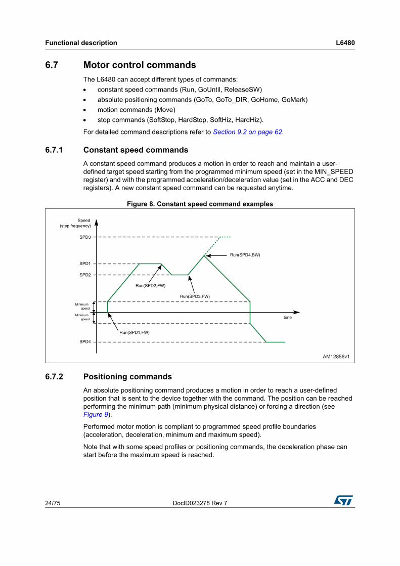
A constant speed command produces a motion in order to reach and maintain a user-defined target speed starting from the programmed minimum speed (set in the MIN_SPEED register) and with the programmed acceleration/deceleration value (set in the ACC and DEC registers). A new constant speed command can be requested anytime.
Figure 8. Constant speed command examples
6.7.2 Positioning commands
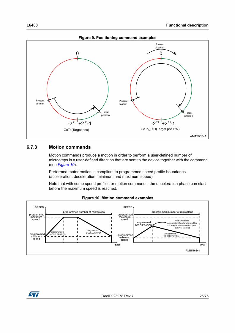
An absolute positioning command produces a motion in order to reach a user-defined position that is sent to the device together with the command. The position can be reached performing the minimum path (minimum physical distance) or forcing a direction (see Figure 9).
Performed motor motion is compliant to programmed speed profile boundaries (acceleration, deceleration, minimum and maximum speed).
Note that with some speed profiles or positioning commands, the deceleration phase can start before the maximum speed is reached.
AM12856v1
SPD1
SPD2
SPD3
SPD4
Run(SPD2,FW)
time
Speed(step frequency)
Run(SPD3,FW)
Run(SPD1,FW)
Run(SPD4,BW)
Minimum speed
Minimum speed
DocID023278 Rev 7 25/75
L6480 Functional description
75
Figure 9. Positioning command examples
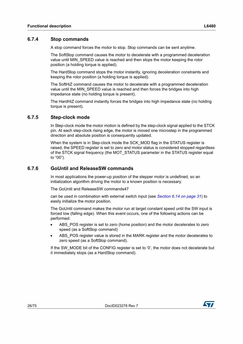
6.7.3 Motion commands
Motion commands produce a motion in order to perform a user-defined number of microsteps in a user-defined direction that are sent to the device together with the command (see Figure 10).
Performed motor motion is compliant to programmed speed profile boundaries (acceleration, deceleration, minimum and maximum speed).
Note that with some speed profiles or motion commands, the deceleration phase can start before the maximum speed is reached.
Figure 10. Motion command examples
programmedACCELERATION
SPEED
programmedmaximum
speed
programmedminimum
speed
time
programmedDECELERATION
programmed number of microsteps
programmedACCELERATION
SPEED
programmedmaximum
speed
programmedminimum
speed
time
programmedDECELERATION
programmed number of microsteps
Note: with someAcceleration/Decelaration profiles the programmed maximum speed
is never reached
AM15163v1
Functional description L6480
26/75 DocID023278 Rev 7
6.7.4 Stop commands
A stop command forces the motor to stop. Stop commands can be sent anytime.
The SoftStop command causes the motor to decelerate with a programmed deceleration value until MIN_SPEED value is reached and then stops the motor keeping the rotor position (a holding torque is applied).
The HardStop command stops the motor instantly, ignoring deceleration constraints and keeping the rotor position (a holding torque is applied).
The SoftHiZ command causes the motor to decelerate with a programmed deceleration value until the MIN_SPEED value is reached and then forces the bridges into high impedance state (no holding torque is present).
The HardHiZ command instantly forces the bridges into high impedance state (no holding torque is present).
6.7.5 Step-clock mode
In Step-clock mode the motor motion is defined by the step-clock signal applied to the STCK pin. At each step-clock rising edge, the motor is moved one microstep in the programmed direction and absolute position is consequently updated.
When the system is in Step-clock mode the SCK_MOD flag in the STATUS register is raised, the SPEED register is set to zero and motor status is considered stopped regardless of the STCK signal frequency (the MOT_STATUS parameter in the STATUS register equal to “00”).
6.7.6 GoUntil and ReleaseSW commands
In most applications the power-up position of the stepper motor is undefined, so an initialization algorithm driving the motor to a known position is necessary.
The GoUntil and ReleaseSW commands47
can be used in combination with external switch input (see Section 6.14 on page 31) to easily initialize the motor position.
The GoUntil command makes the motor run at target constant speed until the SW input is forced low (falling edge). When this event occurs, one of the following actions can be performed:
ABS_POS register is set to zero (home position) and the motor decelerates to zero speed (as a SoftStop command)
ABS_POS register value is stored in the MARK register and the motor decelerates to zero speed (as a SoftStop command).
If the SW_MODE bit of the CONFIG register is set to ‘0’, the motor does not decelerate but it immediately stops (as a HardStop command).
DocID023278 Rev 7 27/75
L6480 Functional description
75
The ReleaseSW command makes the motor run at a programmed minimum speed until the SW input is forced high (rising edge). When this event occurs, one of the following actions can be performed:
ABS_POS register is set to zero (home position) and the motor immediately stops (as a HardStop command)
ABS_POS register value is stored in the MARK register and the motor immediately stops (as a HardStop command).
If the programmed minimum speed is less than 5 step/s, the motor is driven at 5 step/s.
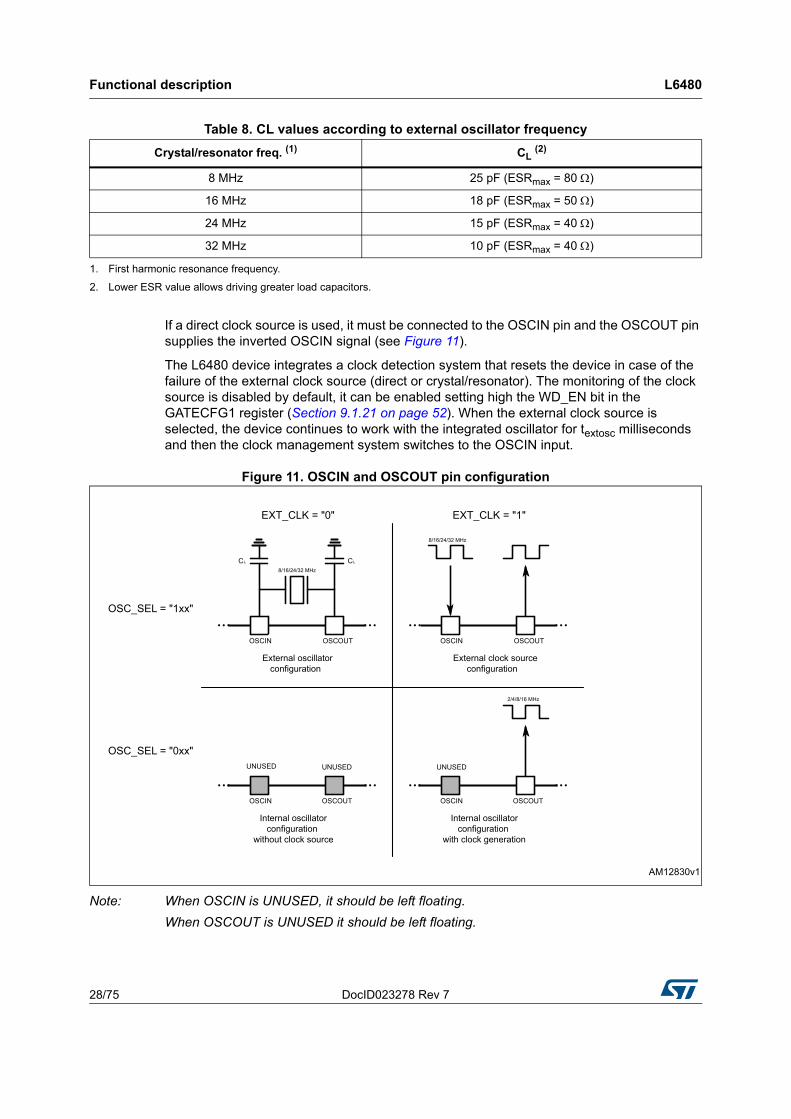
6.8 Internal oscillator and oscillator driver
The control logic clock can be supplied by the internal 16-MHz oscillator, an external oscillator (crystal or ceramic resonator) or a direct clock signal.
These working modes can be selected by EXT_CLK and OSC_SEL parameters in the CONFIG register (see Table 32 on page 55).
At power-up the device starts using the internal oscillator and provides a 2-MHz clock signal on the OSCOUT pin.
Attention: In any case, before changing clock source configuration, a hardware reset is mandatory. Switching to different clock configurations during operation may cause unexpected behavior.
6.8.1 Internal oscillator
In this mode the internal oscillator is activated and OSCIN is unused. If the OSCOUT clock source is enabled, the OSCOUT pin provides a 2, 4, 8 or 16-MHz clock signal (according to OSC_SEL value); otherwise it is unused (see Figure 11).
6.8.2 External clock source
Two types of external clock source can be selected: crystal/ceramic resonator or direct clock source. Four programmable clock frequencies are available for each external clock source: 8, 16, 24 and 32-MHz.
When an external crystal/resonator is selected, the OSCIN and OSCOUT pins are used to drive the crystal/resonator (see Figure 11). The crystal/resonator and load capacitors (CL) must be placed as close as possible to the pins. Refer to Table 8 for the choice of the load capacitor value according to the external oscillator frequency.
Functional description L6480
28/75 DocID023278 Rev 7
If a direct clock source is used, it must be connected to the OSCIN pin and the OSCOUT pin supplies the inverted OSCIN signal (see Figure 11).
The L6480 device integrates a clock detection system that resets the device in case of the failure of the external clock source (direct or crystal/resonator). The monitoring of the clock source is disabled by default, it can be enabled setting high the WD_EN bit in the GATECFG1 register (Section 9.1.21 on page 52). When the external clock source is selected, the device continues to work with the integrated oscillator for textosc milliseconds and then the clock management system switches to the OSCIN input.
Figure 11. OSCIN and OSCOUT pin configuration
Note: When OSCIN is UNUSED, it should be left floating.
When OSCOUT is UNUSED it should be left floating.
Table 8. CL values according to external oscillator frequency
Crystal/resonator freq. (1) CL (2)
8 MHz 25 pF (ESRmax = 80 )
16 MHz 18 pF (ESRmax = 50 )
24 MHz 15 pF (ESRmax = 40 )
32 MHz 10 pF (ESRmax = 40 )
1. First harmonic resonance frequency.
2. Lower ESR value allows driving greater load capacitors.
DocID023278 Rev 7 29/75
L6480 Functional description
75
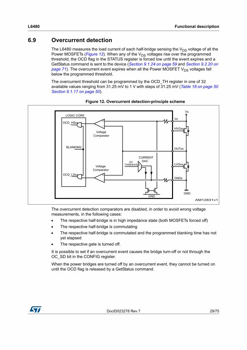
6.9 Overcurrent detection
The L6480 measures the load current of each half-bridge sensing the VDS voltage of all the Power MOSFETs (Figure 12). When any of the VDS voltages rise over the programmed threshold, the OCD flag in the STATUS register is forced low until the event expires and a GetStatus command is sent to the device (Section 9.1.24 on page 59 and Section 9.2.20 on page 71). The overcurrent event expires when all the Power MOSFET VDS voltages fall below the programmed threshold.
The overcurrent threshold can be programmed by the OCD_TH register in one of 32 available values ranging from 31.25 mV to 1 V with steps of 31.25 mV (Table 18 on page 50 Section 9.1.17 on page 50).
Figure 12. Overcurrent detection-principle scheme
The overcurrent detection comparators are disabled, in order to avoid wrong voltage measurements, in the following cases:
The respective half-bridge is in high impedance state (both MOSFETs forced off)
The respective half-bridge is commutating
The respective half-bridge is commutated and the programmed blanking time has not yet elapsed
The respective gate is turned off.
It is possible to set if an overcurrent event causes the bridge turn-off or not through the OC_SD bit in the CONFIG register.
When the power bridges are turned off by an overcurrent event, they cannot be turned on until the OCD flag is released by a GetStatus command.
Functional description L6480
30/75 DocID023278 Rev 7
6.10 Undervoltage lockout (UVLO)
The L6480 provides a programmable gate driver supply voltage UVLO protection. When one of the supply voltages of the gate driver (VCC for the low sides and VBOOT - VS for the high sides) falls below the respective turn-off threshold, an undervoltage event occurs. In this case, all MOSFETs are immediately turned off and the UVLO flag in the STATUS register is forced low.
The UVLO flag is forced low and the MOSFETs are kept off until the gate driver supply voltages return to above the respective turn-on threshold; in this case the undervoltage event expires and the UVLO flag can be released through a GetStatus command.
The UVLO thresholds can be selected between two sets according to the UVLOVAL bit value in the CONFIG register.
6.11 VS undervoltage lockout (UVLO_ADC)
The device provides an undervoltage signal of the integrated ADC input voltage (the UVLO_ADC flag in the STATUS register). When VADCIN falls below the VADC,UVLO value the UVLO_ADC flag is forced low and it is kept in this state until the ADCIN voltage is greater than VADC,UVLO and a GetStatus command is sent to the device.
The ADCIN undervoltage event doesn’t turn off the MOSFETs of the power bridges.
The motor supply voltage undervoltage detection can be performed by means of this feature, connecting the ADCIN pin to VS through a voltage divider as described in Section 7.5 on page 39.
6.12 Thermal warning and thermal shutdown
An integrated sensor allows detection of the internal temperature and implementation of a 3-level protection.
When the Tj(WRN)Set threshold is reached, a warning signal is generated. This is the thermal warning condition and it expires when the temperature falls below the Tj(WRN)Rel threshold.
When the Tj(OFF)Set threshold is reached, all the MOSFETs are turned off and the gate driving circuitry is disabled (Miller clamps are still operative). This condition expires when the temperature falls below the Tj(OFF)Rel threshold.
When the Tj(SD)OFF threshold is reached, all the MOSFETs are turned off using Miller clamps, the internal VCC voltage regulator is disabled and the current capability of the internal VREG voltage regulator is reduced (thermal shutdown). In this condition logic is still
Table 9. UVLO thresholds
ParameterUVLOVAL
0 1
Low-side gate driver supply turn-off threshold (VCCthOff) 6.3 V 10 V
Low-side gate driver supply turn-on threshold (VCCthOn) 6.9 V 10.4 V
High-side gate driver supply turn-off threshold (VBOOTthOff) 5.5 V 8.8 V
High-side gate driver supply turn-on threshold (VBOOTthOff) 6 V 9.2 V
DocID023278 Rev 7 31/75
L6480 Functional description
75
active (if supplied). The thermal shutdown condition only expires when the temperature goes below Tj(SD)ON.
The thermal condition of the device is shown by TH_STATUS bits in the STATUS register (Table 10).
6.13 Reset and standby
The device can be reset and put into Standby mode through the STBY/RESET pin. When it is forced low, all the MOSFETs are turned off (High Z state), the charge pump is stopped, the SPI interface and control logic are disabled and the internal VREG voltage regulator maximum output current is limited; as a result, the L6480 heavily reduces the power consumption. At the same time the register values are reset to their default and all the protection functions are disabled. The STBY/RESET input must be forced low at least for tSTBY,min in order to ensure the complete switch to Standby mode.
On exiting Standby mode, as well as for IC power-up, a delay must be given before applying a new command to allow proper oscillator and charge pump startup. Actual delay could vary according to the values of the charge pump external components.
On exiting Standby mode all the MOSFETs are off and the HiZ flag is high.
The registers can be reset to the default values without putting the device into Standby mode through the ResetDevice command (Section 9.2.14 on page 69).
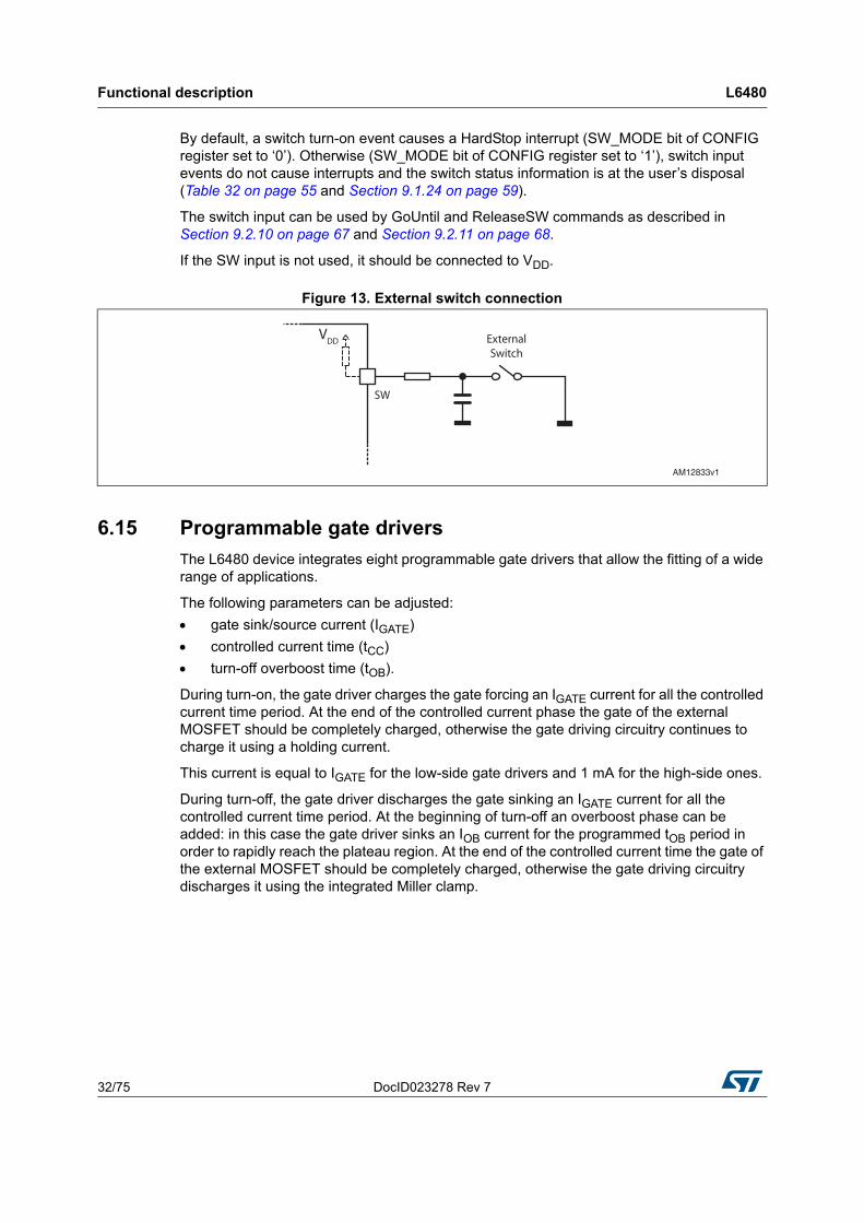
6.14 External switch (SW pin)
The SW input is internally pulled up to VDD and detects if the pin is open or connected to ground (see Figure 13).
The SW_F bit of the STATUS register indicates if the switch is open (‘0’) or closed (‘1’) (Section 9.1.24 on page 59); the bit value is refreshed at every system clock cycle (125 ns). The SW_EVN flag of the STATUS register is raised when a switch turn-on event (SW input falling edge) is detected (Section 9.1.24). A GetStatus command releases the SW_EVN flag (Section 9.2.20 on page 71).
Table 10. Thermal protection summarizing table
State Set condition Release condition Description TH_STATUS
Normal Normal operation state 00
Warning Tj > Tj(WRN)Set Tj > Tj(WRN)RelTemperature warning: operation is not limited
01
Bridge shutdown Tj > Tj(OFF)Set Tj > Tj(OFF)Rel
High temperature protection: the MOSFETs are turned off and the gate drivers are disabled
10
Device shutdown Tj > Tj(SD)Set Tj > Tj(SD)Rel
Overtemperature protection: the MOSFETs are turned off, the gate drivers are disabled, the internal VCC voltage regulator is disabled, the current capability of the internal VREG voltage regulator is limited, and the charge pump is disabled
11
Functional description L6480
32/75 DocID023278 Rev 7
By default, a switch turn-on event causes a HardStop interrupt (SW_MODE bit of CONFIG register set to ‘0’). Otherwise (SW_MODE bit of CONFIG register set to ‘1’), switch input events do not cause interrupts and the switch status information is at the user’s disposal (Table 32 on page 55 and Section 9.1.24 on page 59).
The switch input can be used by GoUntil and ReleaseSW commands as described in Section 9.2.10 on page 67 and Section 9.2.11 on page 68.
If the SW input is not used, it should be connected to VDD.
6.15 Programmable gate drivers
The L6480 device integrates eight programmable gate drivers that allow the fitting of a wide range of applications.
The following parameters can be adjusted:
gate sink/source current (IGATE)
controlled current time (tCC)
turn-off overboost time (tOB).
During turn-on, the gate driver charges the gate forcing an IGATE current for all the controlled current time period. At the end of the controlled current phase the gate of the external MOSFET should be completely charged, otherwise the gate driving circuitry continues to charge it using a holding current.
This current is equal to IGATE for the low-side gate drivers and 1 mA for the high-side ones.
During turn-off, the gate driver discharges the gate sinking an IGATE current for all the controlled current time period. At the beginning of turn-off an overboost phase can be added: in this case the gate driver sinks an IOB current for the programmed tOB period in order to rapidly reach the plateau region. At the end of the controlled current time the gate of the external MOSFET should be completely charged, otherwise the gate driving circuitry discharges it using the integrated Miller clamp.
Figure 13. External switch connection
AM12833v1
ExternalSwitch
SW
VDD
DocID023278 Rev 7 33/75
L6480 Functional description
75
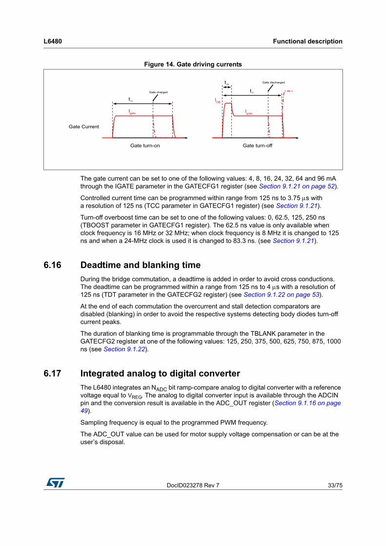
The gate current can be set to one of the following values: 4, 8, 16, 24, 32, 64 and 96 mA through the IGATE parameter in the GATECFG1 register (see Section 9.1.21 on page 52).
Controlled current time can be programmed within range from 125 ns to 3.75 s with a resolution of 125 ns (TCC parameter in GATECFG1 register) (see Section 9.1.21).
Turn-off overboost time can be set to one of the following values: 0, 62.5, 125, 250 ns (TBOOST parameter in GATECFG1 register). The 62.5 ns value is only available when clock frequency is 16 MHz or 32 MHz; when clock frequency is 8 MHz it is changed to 125 ns and when a 24-MHz clock is used it is changed to 83.3 ns. (see Section 9.1.21).
6.16 Deadtime and blanking time
During the bridge commutation, a deadtime is added in order to avoid cross conductions. The deadtime can be programmed within a range from 125 ns to 4 s with a resolution of 125 ns (TDT parameter in the GATECFG2 register) (see Section 9.1.22 on page 53).
At the end of each commutation the overcurrent and stall detection comparators are disabled (blanking) in order to avoid the respective systems detecting body diodes turn-off current peaks.
The duration of blanking time is programmable through the TBLANK parameter in the GATECFG2 register at one of the following values: 125, 250, 375, 500, 625, 750, 875, 1000 ns (see Section 9.1.22).
6.17 Integrated analog to digital converter
The L6480 integrates an NADC bit ramp-compare analog to digital converter with a reference voltage equal to VREG. The analog to digital converter input is available through the ADCIN pin and the conversion result is available in the ADC_OUT register (Section 9.1.16 on page 49).
Sampling frequency is equal to the programmed PWM frequency.
The ADC_OUT value can be used for motor supply voltage compensation or can be at the user’s disposal.
Figure 14. Gate driving currents
Functional description L6480
34/75 DocID023278 Rev 7
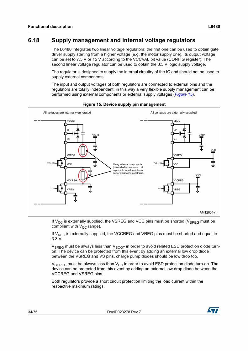
6.18 Supply management and internal voltage regulators
The L6480 integrates two linear voltage regulators: the first one can be used to obtain gate driver supply starting from a higher voltage (e.g. the motor supply one). Its output voltage can be set to 7.5 V or 15 V according to the VCCVAL bit value (CONFIG register). The second linear voltage regulator can be used to obtain the 3.3 V logic supply voltage.
The regulator is designed to supply the internal circuitry of the IC and should not be used to supply external components.
The input and output voltages of both regulators are connected to external pins and the regulators are totally independent: in this way a very flexible supply management can be performed using external components or external supply voltages (Figure 15).
Figure 15. Device supply pin management
If VCC is externally supplied, the VSREG and VCC pins must be shorted (VSREG must be compliant with VCC range).
If VREG is externally supplied, the VCCREG and VREG pins must be shorted and equal to 3.3 V.
VSREG must be always less than VBOOT in order to avoid related ESD protection diode turn-on. The device can be protected from this event by adding an external low drop diode between the VSREG and VS pins, charge pump diodes should be low drop too.
VCCREG must be always less than VCC in order to avoid ESD protection diode turn-on. The device can be protected from this event by adding an external low drop diode between the VCCREG and VSREG pins.
Both regulators provide a short circuit protection limiting the load current within the respective maximum ratings.
DocID023278 Rev 7 35/75
L6480 Functional description
75
6.19 BUSY/SYNC pin
This pin is an open drain output which can be used as busy flag or synchronization signal according to the SYNC_EN bit value (STEP_MODE register) (see Section 9.1.19 on page 50).
6.20 FLAG pin
By default, an internal open drain transistor pulls the FLAG pin to ground when at least one of the following conditions occurs:
Power-up or standby/reset exit
Stall detection on bridge A
Stall detection on bridge B
Overcurrent detection
Thermal warning
Thermal shutdown
UVLO
UVLO on ADC input
Switch turn-on event
Command error.
It is possible to mask one or more alarm conditions by programming the ALARM_EN register (see Section 9.1.20 on page 52 and Table 23 on page 52). If the corresponding bit of the ALARM_EN register is low, the alarm condition is masked and it does not cause a FLAG pin transition; all other actions imposed by alarm conditions are performed anyway. In case of daisy chain configuration, FLAG pins of different ICs can be or-wired to save host controller GPIOs.
Phase current control L6480
36/75 DocID023278 Rev 7
7 Phase current control
The L6480 controls the phase current applying a sinusoidal voltage to motor windings. Phase current amplitude is not directly controlled but depends on phase voltage amplitude, load torque, motor electrical characteristics and rotation speed. Sine wave amplitude is proportional to the motor supply voltage multiplied by a coefficient (KVAL). KVAL ranges from 0 to 100% and the sine wave amplitude can be obtained through the following formula:
Equation 1
Different KVAL values can be programmed for acceleration, deceleration and constant speed phases and when the motor is stopped (HOLD phase) through KVAL_ACC, KVAL_DEC, KVAL_RUN and KVAL_HOLD registers (Section 9.1.10 on page 47). KVAL value is calculated according to the following formula:
Equation 2
where KVAL_X is the starting KVAL value programmed for the present motion phase (KVAL_ACC, KVAL_DEC, KVAL_RUN or KVAL_HOLD), BEMF_COMP is the BEMF compensation curve value, VSCOMP and K_THERM are the motor supply voltage and winding resistance compensation factors and microstep is the current microstep value (fraction of target peak current).
The L6480 offers various methods to guarantee a stable current value, allowing the compensation of:
low speed distortion (Section 7.3)
back electromotive force (Section 7.4)
motor supply voltage variation (Section 7.5)
windings resistance variation (Section 7.6 on page 40).
7.1 PWM sine wave generators
The two voltage sine waves applied to the stepper motor phases are generated by two PWM modulators.
The PWM frequency (fPWM) is proportional to the oscillator frequency (fOSC) and can be obtained through the following formula:
Equation 3
'N' is the integer division factor and 'm' is the multiplication factor. 'N' and 'm' values can be programmed by F_PWM_INT and F_PWM_DEC parameters in the CONFIG register (see Table 38 on page 57 and Table 39 on page 57, Section 9.1.23 on page 54).
Available PWM frequencies are listed in Section 9.1.23 from Table 40 on page 58 to Table 43 on page 59.
VOUT VS KVAL=
KVAL KVAL_X BEMF_COMP+ VSCOMP K_THERM microst ep=
fPWM
fOSC
512 N------------------ m=
DocID023278 Rev 7 37/75
L6480 Phase current control
75
7.2 Sensorless stall detection
The L6480 is able to detect a motor stall caused by an excessive load torque. When the motor is driven using the voltage mode approach, a stall condition corresponds to an unexpected increase of the phase current. Imposing a current threshold slightly above the operative current, it is possible to detect the stall condition without speed or position sensors.
The L6480 measures the load current of each phase sensing the VDS voltage of the low-side Power MOSFETs. When any of the VDS voltages rise over the programmed threshold, the STEP_LOSS_X flag in the STATUS register of the respective bridge (STEP_LOSS_A or STEP_LOSS_B) is forced low. The failure flag is kept low until the VDS voltages fall below the programmed threshold and a GetStatus command is sent to the device (Section 9.1.24 on page 59 and Section 9.2.20 on page 71).
The stall detection threshold can be programmed in one of 32 available values ranging from 31.25 mV to 1 V with steps of 31.25 mV (see Section 9.1.18 on page 50).
Stall detection comparators are disabled, in order to avoid wrong voltage measurements, in the following cases:
The respective half-bridge is in high impedance state (both MOSFETs forced off)
The respective half-bridge is commutating
The respective half-bridge is commutated and the programmed blanking time has not yet elapsed
The respective low-side gate is turned off.
7.3 Low speed optimization
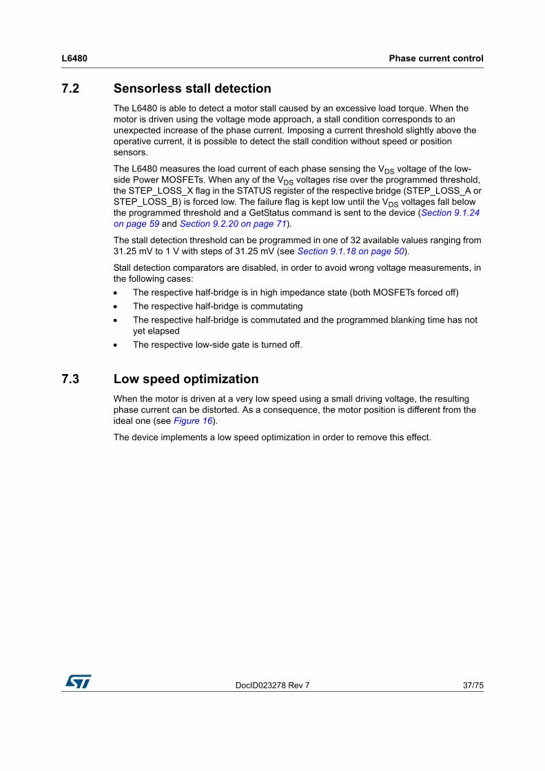
When the motor is driven at a very low speed using a small driving voltage, the resulting phase current can be distorted. As a consequence, the motor position is different from the ideal one (see Figure 16).
The device implements a low speed optimization in order to remove this effect.
Phase current control L6480
38/75 DocID023278 Rev 7
Figure 16. Current distortion and compensation
The optimization can be enabled setting high the LSPD_OPT bit in the MIN_SPEED register (Section 9.1.8 on page 46) and is active in a speed range from zero to MIN_SPEED. When low speed optimization is enabled, speed profile minimum speed is forced to zero.
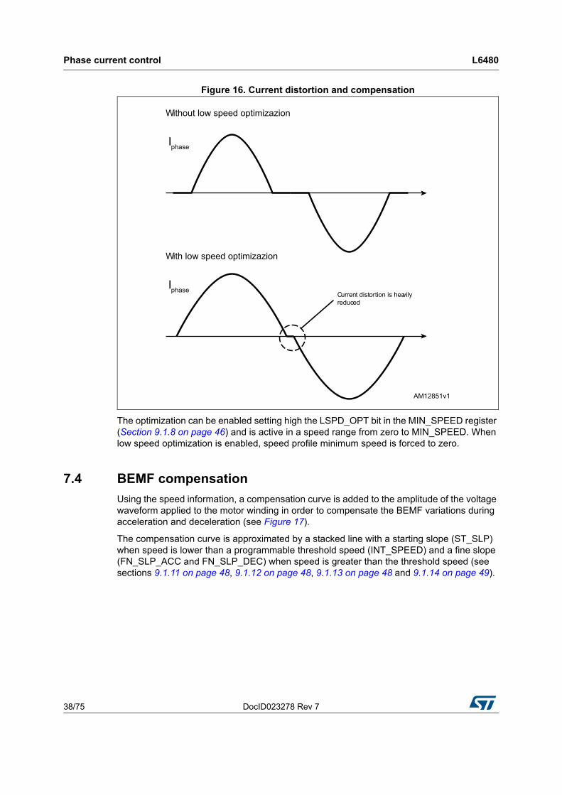
7.4 BEMF compensation
Using the speed information, a compensation curve is added to the amplitude of the voltage waveform applied to the motor winding in order to compensate the BEMF variations during acceleration and deceleration (see Figure 17).
The compensation curve is approximated by a stacked line with a starting slope (ST_SLP) when speed is lower than a programmable threshold speed (INT_SPEED) and a fine slope (FN_SLP_ACC and FN_SLP_DEC) when speed is greater than the threshold speed (see sections 9.1.11 on page 48, 9.1.12 on page 48, 9.1.13 on page 48 and 9.1.14 on page 49).
DocID023278 Rev 7 39/75
L6480 Phase current control
75
To obtain different current values during acceleration and deceleration phase, two different final slope values, and consequently two different compensation curves, can be programmed.
Acceleration compensation curve is applied when the motor runs. No BEMF compensation is applied when the motor is stopped.
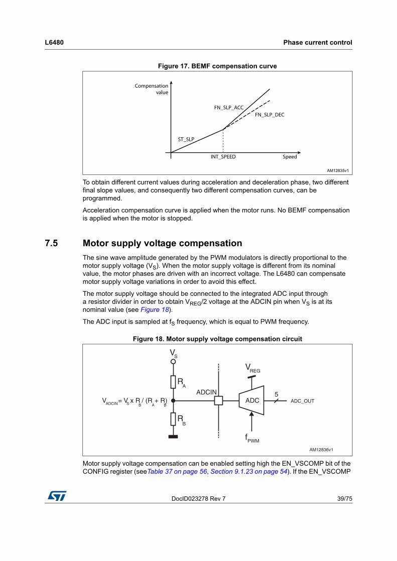
7.5 Motor supply voltage compensation
The sine wave amplitude generated by the PWM modulators is directly proportional to the motor supply voltage (VS). When the motor supply voltage is different from its nominal value, the motor phases are driven with an incorrect voltage. The L6480 can compensate motor supply voltage variations in order to avoid this effect.
The motor supply voltage should be connected to the integrated ADC input through a resistor divider in order to obtain VREG/2 voltage at the ADCIN pin when VS is at its nominal value (see Figure 18).
The ADC input is sampled at fS frequency, which is equal to PWM frequency.
Motor supply voltage compensation can be enabled setting high the EN_VSCOMP bit of the CONFIG register (seeTable 37 on page 56, Section 9.1.23 on page 54). If the EN_VSCOMP
Figure 17. BEMF compensation curve
Figure 18. Motor supply voltage compensation circuit
AM12836v1
ADCINADC
5
fPWM
ADC_OUT
VS
VREG
RA
RB
VADCIN = VS x RB / (R
A + R
B)
Phase current control L6480
40/75 DocID023278 Rev 7
bit is low, the compensation is disabled and the internal analog to digital converter is at the user’s disposal; the sampling rate is always equal to PWM frequency.
7.6 Winding resistance thermal drift compensation
The higher the winding resistance the greater the voltage to be applied in order to obtain the same phase current.
The L6480 integrates a register (K_THERM) which can be used to compensate phase resistance increment due to temperature rising.
The value in the K_THERM register (Section 9.1.15 on page 49) multiplies duty cycle value allowing the higher phase resistance value to be faced.
The compensation algorithm and the eventual motor temperature measurement should be implemented by microcontroller firmware.
DocID023278 Rev 7 41/75
L6480 Serial interface
75
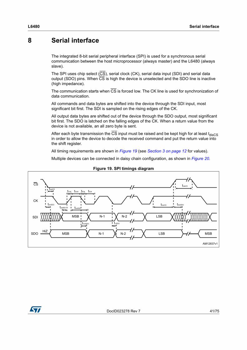
8 Serial interface
The integrated 8-bit serial peripheral interface (SPI) is used for a synchronous serial communication between the host microprocessor (always master) and the L6480 (always slave).
The SPI uses chip select (CS), serial clock (CK), serial data input (SDI) and serial data output (SDO) pins. When CS is high the device is unselected and the SDO line is inactive (high impedance).
The communication starts when CS is forced low. The CK line is used for synchronization of data communication.
All commands and data bytes are shifted into the device through the SDI input, most significant bit first. The SDI is sampled on the rising edges of the CK.
All output data bytes are shifted out of the device through the SDO output, most significant bit first. The SDO is latched on the falling edges of the CK. When a return value from the device is not available, an all zero byte is sent.
After each byte transmission the CS input must be raised and be kept high for at least tdisCS in order to allow the device to decode the received command and put the return value into the shift register.
All timing requirements are shown in Figure 19 (see Section 3 on page 12 for values).
Multiple devices can be connected in daisy chain configuration, as shown in Figure 20.
Figure 19. SPI timings diagram
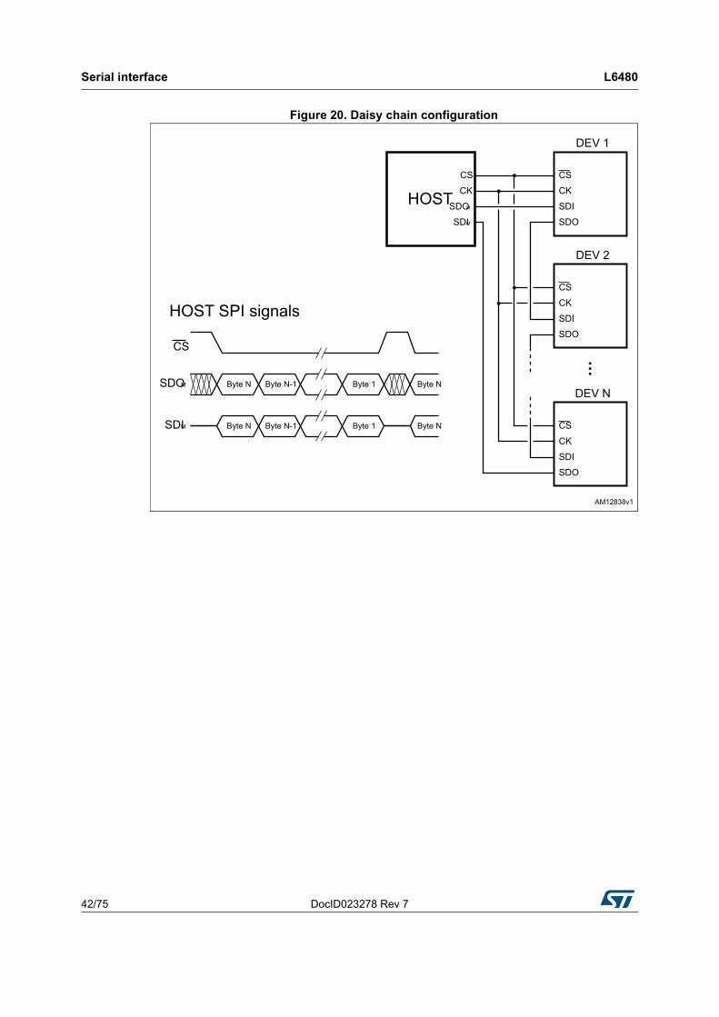
Serial interface L6480
42/75 DocID023278 Rev 7
Figure 20. Daisy chain configuration
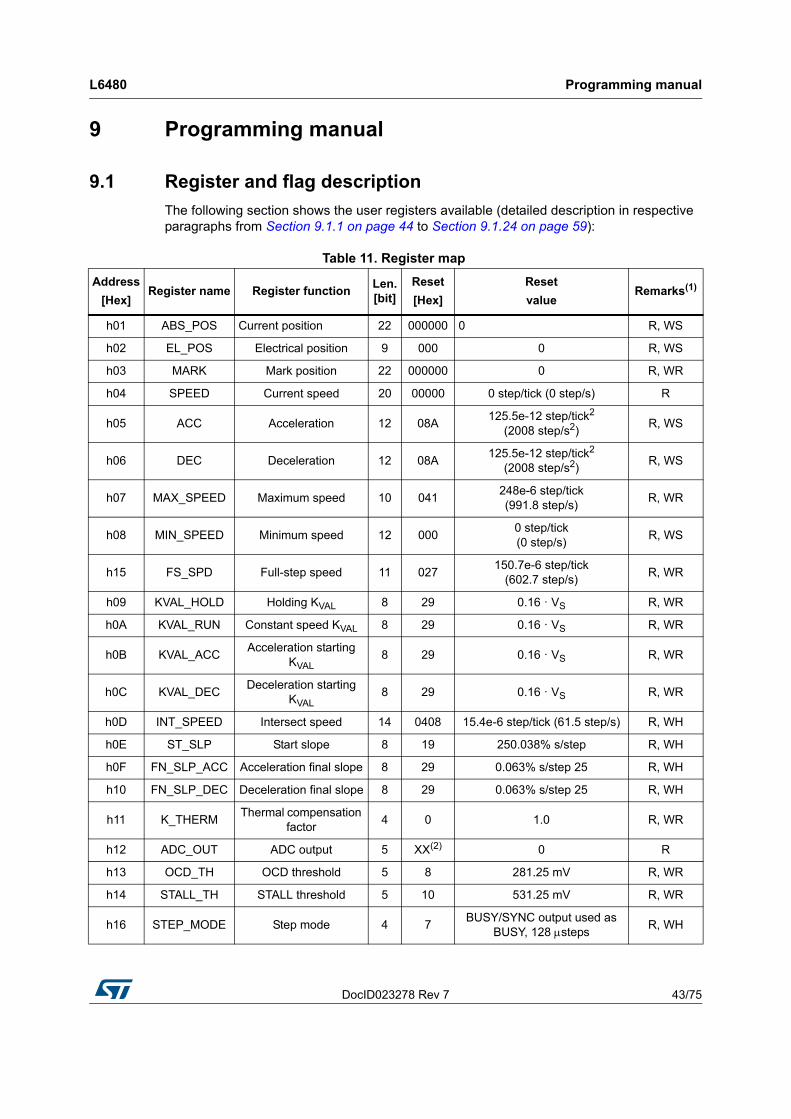
DocID023278 Rev 7 43/75
L6480 Programming manual
75
9 Programming manual
9.1 Register and flag description
The following section shows the user registers available (detailed description in respective paragraphs from Section 9.1.1 on page 44 to Section 9.1.24 on page 59):
Table 11. Register map
Address
[Hex]Register name Register function
Len.[bit]
Reset
[Hex]
Reset
valueRemarks(1)
h01 ABS_POS Current position 22 000000 0 R, WS
h02 EL_POS Electrical position 9 000 0 R, WS
h03 MARK Mark position 22 000000 0 R, WR
h04 SPEED Current speed 20 00000 0 step/tick (0 step/s) R
h05 ACC Acceleration 12 08A125.5e-12 step/tick2
(2008 step/s2)R, WS
h06 DEC Deceleration 12 08A125.5e-12 step/tick2
(2008 step/s2)R, WS
h07 MAX_SPEED Maximum speed 10 041248e-6 step/tick(991.8 step/s)
R, WR
h08 MIN_SPEED Minimum speed 12 0000 step/tick(0 step/s)
R, WS
h15 FS_SPD Full-step speed 11 027150.7e-6 step/tick
(602.7 step/s)R, WR
h09 KVAL_HOLD Holding KVAL 8 29 0.16 · VS R, WR
h0A KVAL_RUN Constant speed KVAL 8 29 0.16 · VS R, WR
h0B KVAL_ACCAcceleration starting
KVAL8 29 0.16 · VS R, WR
h0C KVAL_DECDeceleration starting
KVAL8 29 0.16 · VS R, WR
h0D INT_SPEED Intersect speed 14 0408 15.4e-6 step/tick (61.5 step/s) R, WH
h0E ST_SLP Start slope 8 19 250.038% s/step R, WH
h0F FN_SLP_ACC Acceleration final slope 8 29 0.063% s/step 25 R, WH
h10 FN_SLP_DEC Deceleration final slope 8 29 0.063% s/step 25 R, WH
h11 K_THERMThermal compensation
factor4 0 1.0 R, WR
h12 ADC_OUT ADC output 5 XX(2) 0 R
h13 OCD_TH OCD threshold 5 8 281.25 mV R, WR
h14 STALL_TH STALL threshold 5 10 531.25 mV R, WR
h16 STEP_MODE Step mode 4 7BUSY/SYNC output used as
BUSY, 128 stepsR, WH
Programming manual L6480
44/75 DocID023278 Rev 7
9.1.1 ABS_POS
The ABS_POS register contains the current motor absolute position in agreement with the selected step mode; the stored value unit is equal to the selected step mode (full, half, quarter, etc.). The value is in 2's complement format and it ranges from -221 to +221-1.
At power-on the register is initialized to “0” (HOME position).
Any attempt to write the register when the motor is running causes the command to be ignored and the CMD_ERROR flag to rise (Section 9.1.24 on page 59).
9.1.2 EL_POS
The EL_POS register contains the current electrical position of the motor. The two MSbits indicate the current step and the other bits indicate the current microstep (expressed in step/128) within the step.
h17 ALARM_EN Alarms enables 8 FF All alarms enabled R, WS
h18 GATECFG1Gate driver
configuration11 0
Igate = 4 mA, tCC = 125 ns, no boost
R, WH
h19 GATECFG2Gate driver
configuration8 0 tBLANK = 125 ns, tDT = 125 ns R, WH
h1A CONFIG IC configuration 16 2C88
Internal 16 MHz oscillator (OSCOUT at 2 MHz),
SW event causes HardStop,
motor supply voltage compensation disabled,
overcurrent shutdown,
VCC = 7.5 V,
UVLO threshold low,
fPWM = fOSC / 1024
R, WH
h1B STATUS Status 16 XXXX(2)
High impedance state,
motor stopped,
reverse direction,
all fault flags released UVLO/Reset flag set
R
1. R: readable, WH: writable, only when outputs are in high impedance, WS: writable only when motor is stopped, WR: always writable.
2. According to startup conditions.
Table 11. Register map (continued)
Address
[Hex]Register name Register function
Len.[bit]
Reset
[Hex]
Reset
valueRemarks(1)
Table 12. EL_POS register
Bit 8 Bit 7 Bit 6 Bit 5 Bit 4 Bit 3 Bit 2 Bit 1 Bit 0
STEP MICROSTEP
DocID023278 Rev 7 45/75
L6480 Programming manual
75
When the EL_POS register is written by the user the new electrical position is instantly imposed. When the EL_POS register is written, its value must be masked in order to match with the step mode selected in the STEP_MODE register in order to avoid a wrong microstep value generation (Section 9.1.19 on page 50); otherwise the resulting microstep sequence is incorrect.
Any attempt to write the register when the motor is running causes the command to be ignored and the CMD_ERROR flag to rise (Section 9.1.24 on page 59).
9.1.3 MARK
The MARK register contains an absolute position called MARK, according to the selected step mode; the stored value unit is equal to the selected step mode (full, half, quarter, etc.). It is in 2's complement format and it ranges from -221 to +221-1.
9.1.4 SPEED
The SPEED register contains the current motor speed, expressed in step/tick (format unsigned fixed point 0.28).
In order to convert the SPEED value in step/s the following formula can be used:
Equation 4
where SPEED is the integer number stored in the register and tick is 250 ns.
The available range is from 0 to 15625 step/s with a resolution of 0.015 step/s.
Note: The range effectively available to the user is limited by the MAX_SPEED parameter.
Any attempt to write the register causes the command to be ignored and the CMD_ERROR flag to rise (Section 9.1.24).
9.1.5 ACC
The ACC register contains the speed profile acceleration expressed in step/tick2 (format unsigned fixed point 0.40).
In order to convert the ACC value in step/s2 the following formula can be used:
Equation 5
where ACC is the integer number stored in the register and tick is 250 ns.
The available range is from 14.55 to 59590 step/s2 with a resolution of 14.55 step/s2.
The 0xFFF value of the register is reserved and it should never be used.
Any attempt to write to the register when the motor is running causes the command to be ignored and the CMD_ERROR flag to rise (Section 9.1.24).
step/s SPEED 228–
tick-------------------------------------=
step/s2 ACC 2
40–
tick2
-----------------------------=
Programming manual L6480
46/75 DocID023278 Rev 7
9.1.6 DEC
The DEC register contains the speed profile deceleration expressed in step/tick2 (format unsigned fixed point 0.40).
In order to convert the DEC value in step/s2 the following formula can be used:
Equation 6
where DEC is the integer number stored in the register and tick is 250 ns.
The available range is from 14.55to 59590 step/s2 with a resolution of 14.55 step/s2.
Any attempt to write the register when the motor is running causes the command to be ignored and the CMD_ERROR flag to rise (Section 9.1.24 on page 59).
9.1.7 MAX_SPEED
The MAX_SPEED register contains the speed profile maximum speed expressed in step/tick (format unsigned fixed point 0.18).
In order to convert it in step/s, the following formula can be used:
Equation 7
where MAX_SPEED is the integer number stored in the register and tick is 250 ns.
The available range is from 15.25 to 15610 step/s with a resolution of 15.25 step/s.
9.1.8 MIN_SPEED
The MIN_SPEED register contains the following parameters:
The MIN_SPEED parameter contains the speed profile minimum speed. Its value is expressed in step/tick and to convert it in step/s the following formula can be used:
Equation 8
where MIN_SPEED is the integer number stored in the register and tick is the ramp 250 ns.
The available range is from 0 to 976.3 step/s with a resolution of 0.238 step/s.
step/s2 DEC 2
40–
tick2
-----------------------------=
step/s MAX_SPEED 218–
tick-----------------------------------------------------=
Table 13. MIN_SPEED register
Bit 12 Bit 11 Bit 10 Bit 9 Bit 8 Bit 7 Bit 6 Bit 5 Bit 4 Bit 3 Bit 2 Bit 1 Bit 0
LSPD_OPT MIN_SPEED
step/s MIN_SPEED 224–
tick---------------------------------------------------=
DocID023278 Rev 7 47/75
L6480 Programming manual
75
When the LSPD_OPT bit is set high, low speed optimization feature is enabled and the MIN_SPEED value indicates the speed threshold below which the compensation works. In this case the minimum speed of the speed profile is set to zero.
Any attempt to write the register when the motor is running causes the CMD_ERROR flag to rise.
9.1.9 FS_SPD
The FS_SPD register contains the following parameters:
The FS_SPD threshold speed value over which the step mode is automatically switched to full-step two-phase on. Its value is expressed in step/tick (format unsigned fixed point 0.18) and to convert it in step/s the following formula can be used:
Equation 9
If FS_SPD value is set to hFF (max.) the system always works in Microstepping mode (SPEED must go over the threshold to switch to Full-step mode). Setting FS_SPD to zero does not have the same effect as setting the step mode to full-step two-phase on: the zero FS_SPD value is equivalent to a speed threshold of about 7.63 step/s.
The available range is from 7.63 to 15625 step/s with a resolution of 15.25 step/s.
The BOOST_MODE bit sets the amplitude of the voltage squarewave during the full-step operation (see Section on page 22).
9.1.10 KVAL_HOLD, KVAL_RUN, KVAL_ACC and KVAL_DEC
The KVAL_HOLD register contains the KVAL value that is assigned to the PWM modulators when the motor is stopped (compensations excluded).
The KVAL_RUN register contains the KVAL value that is assigned to the PWM modulators when the motor is running at constant speed (compensations excluded).
The KVAL_ACC register contains the starting KVAL value that can be assigned to the PWM modulators during acceleration (compensations excluded).
The KVAL_DEC register contains the starting KVAL value that can be assigned to the PWM modulators during deceleration (compensations excluded).
The available range is from 0 to 0.996 x VS with a resolution of 0.004 x VS, as shown in Table 15.
Table 14. FS_SPD register
Bit 10 Bit 9 Bit 8 Bit 7 Bit 6 Bit 5 Bit 4 Bit 3 Bit 2 Bit 1 Bit 0
BOOST_MODE FS_SPD
step/s FS_SPD 0.5+ 218–
tick-----------------------------------------------------------=
Programming manual L6480
48/75 DocID023278 Rev 7
9.1.11 INT_SPEED
The INT_SPEED register contains the speed value at which the BEMF compensation curve changes slope (Section 7.4 on page 38 for details). Its value is expressed in step/tick and to convert it in [step/s] the following formula can be used:
Equation 10
where INT_SPEED is the integer number stored in the register and tick is 250 ns.
The available range is from 0 to 976.5 step/s with a resolution of 0.0596 step/s.
Any attempt to write the register when the motor is running causes the command to be ignored and the CMD_ERROR flag to rise (Section 9.1.24 on page 59).
9.1.12 ST_SLP
The ST_SLP register contains the BEMF compensation curve slope that is used when the speed is lower than the intersect speed (Section 7.4). Its value is expressed in s/step and the available range is from 0 to 0.004 with a resolution of 0.000015.
When ST_SLP, FN_SLP_ACC and FN_SLP_DEC parameters are set to zero, no BEMF compensation is performed.
Any attempt to write the register when the motor is running causes the command to be ignored and the CMD_ERROR flag to rise (Section 9.1.24).
9.1.13 FN_SLP_ACC
The FN_SLP_ACC register contains the BEMF compensation curve slope that is used when the speed is greater than the intersect speed during acceleration (Section 7.4 for details). Its value is expressed in s/step and the available range is from 0 to 0.004 with a resolution of 0.000015.
When ST_SLP, FN_SLP_ACC and FN_SLP_DEC parameters are set to zero, no BEMF compensation is performed.
Any attempt to write the register when the motor is running causes the command to be ignored and the CMD_ERROR flag to rise (Section 9.1.24).
Table 15. Voltage amplitude regulation registers
KVAL_X [7…0] Output voltage
0 0 0 0 0 0 0 0 0
0 0 0 0 0 0 0 1 VS x (1/256)… … … … … … … … …
1 1 1 1 1 1 1 0 VS x (254/256)
1 1 1 1 1 1 1 1 VS x (255/256)
step/s INT_SPEED 218–
tick--------------------------------------------------=
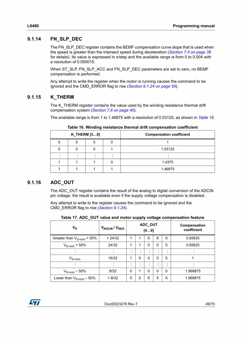
DocID023278 Rev 7 49/75
L6480 Programming manual
75
9.1.14 FN_SLP_DEC
The FN_SLP_DEC register contains the BEMF compensation curve slope that is used when the speed is greater than the intersect speed during deceleration (Section 7.4 on page 38 for details). Its value is expressed in s/step and the available range is from 0 to 0.004 with a resolution of 0.000015.
When ST_SLP, FN_SLP_ACC and FN_SLP_DEC parameters are set to zero, no BEMF compensation is performed.
Any attempt to write the register when the motor is running causes the command to be ignored and the CMD_ERROR flag to rise (Section 9.1.24 on page 59).
9.1.15 K_THERM
The K_THERM register contains the value used by the winding resistance thermal drift compensation system (Section 7.6 on page 40).
The available range is from 1 to 1.46875 with a resolution of 0.03125, as shown in Table 16.
9.1.16 ADC_OUT
The ADC_OUT register contains the result of the analog to digital conversion of the ADCIN pin voltage; the result is available even if the supply voltage compensation is disabled.
Any attempt to write to the register causes the command to be ignored and the CMD_ERROR flag to rise (Section 9.1.24).
Table 16. Winding resistance thermal drift compensation coefficient
K_THERM [3…0] Compensation coefficient
0 0 0 0 1
0 0 0 1 1.03125
… … … … …1 1 1 0 1.4375
1 1 1 1 1.46875
Table 17. ADC_OUT value and motor supply voltage compensation feature
VS VADCIN / VREGADC_OUT
[4…0]Compensation
coefficient
Greater than VS,nom + 50% > 24/32 1 1 X X X 0.65625
VS,nom + 50% 24/32 1 1 0 0 0 0.65625
… … … … … … … …
VS,nom 16/32 1 0 0 0 0 1
… … … … … … … …
VS,nom – 50% 8/32 0 1 0 0 0 1.968875
Lower than VS,nom – 50% < 8/32 0 0 X X X 1.968875
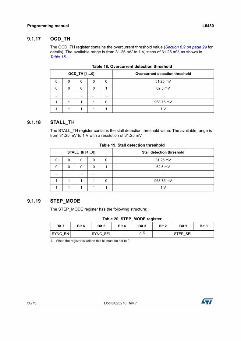
Programming manual L6480
50/75 DocID023278 Rev 7
9.1.17 OCD_TH
The OCD_TH register contains the overcurrent threshold value (Section 6.9 on page 29 for details). The available range is from 31.25 mV to 1 V, steps of 31.25 mV, as shown in Table 18.
9.1.18 STALL_TH
The STALL_TH register contains the stall detection threshold value. The available range is from 31.25 mV to 1 V with a resolution of 31.25 mV.
9.1.19 STEP_MODE
The STEP_MODE register has the following structure:
Table 18. Overcurrent detection threshold
OCD_TH [4…0] Overcurrent detection threshold
0 0 0 0 0 31.25 mV
0 0 0 0 1 62.5 mV
… … … … … …
1 1 1 1 0 968.75 mV
1 1 1 1 1 1 V
Table 19. Stall detection threshold
STALL_th [4…0] Stall detection threshold
0 0 0 0 0 31.25 mV
0 0 0 0 1 62.5 mV
… … … … … …
1 1 1 1 0 968.75 mV
1 1 1 1 1 1 V
Table 20. STEP_MODE register
Bit 7 Bit 6 Bit 5 Bit 4 Bit 3 Bit 2 Bit 1 Bit 0
SYNC_EN SYNC_SEL 0(1)
1. When the register is written this bit must be set to 0.
STEP_SEL
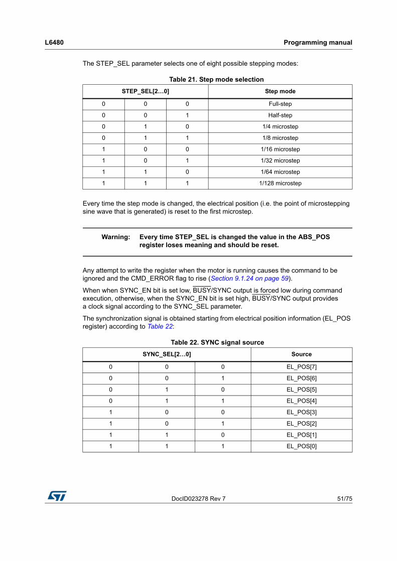
DocID023278 Rev 7 51/75
L6480 Programming manual
75
The STEP_SEL parameter selects one of eight possible stepping modes:
Every time the step mode is changed, the electrical position (i.e. the point of microstepping sine wave that is generated) is reset to the first microstep.
Warning: Every time STEP_SEL is changed the value in the ABS_POS register loses meaning and should be reset.
Any attempt to write the register when the motor is running causes the command to be ignored and the CMD_ERROR flag to rise (Section 9.1.24 on page 59).
When when SYNC_EN bit is set low, BUSY/SYNC output is forced low during command execution, otherwise, when the SYNC_EN bit is set high, BUSY/SYNC output provides a clock signal according to the SYNC_SEL parameter.
The synchronization signal is obtained starting from electrical position information (EL_POS register) according to Table 22:
Table 21. Step mode selection
STEP_SEL[2…0] Step mode
0 0 0 Full-step
0 0 1 Half-step
0 1 0 1/4 microstep
0 1 1 1/8 microstep
1 0 0 1/16 microstep
1 0 1 1/32 microstep
1 1 0 1/64 microstep
1 1 1 1/128 microstep
Table 22. SYNC signal source
SYNC_SEL[2…0] Source
0 0 0 EL_POS[7]
0 0 1 EL_POS[6]
0 1 0 EL_POS[5]
0 1 1 EL_POS[4]
1 0 0 EL_POS[3]
1 0 1 EL_POS[2]
1 1 0 EL_POS[1]
1 1 1 EL_POS[0]
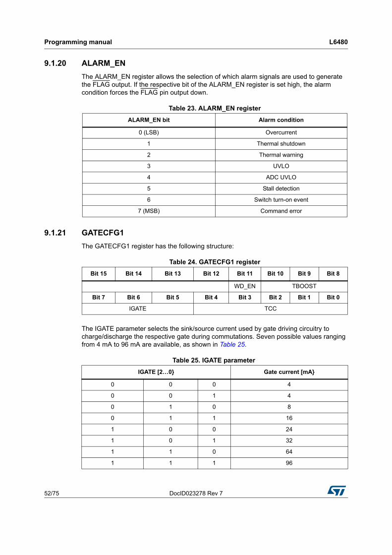
Programming manual L6480
52/75 DocID023278 Rev 7
9.1.20 ALARM_EN
The ALARM_EN register allows the selection of which alarm signals are used to generate the FLAG output. If the respective bit of the ALARM_EN register is set high, the alarm condition forces the FLAG pin output down.
9.1.21 GATECFG1
The GATECFG1 register has the following structure:
The IGATE parameter selects the sink/source current used by gate driving circuitry to charge/discharge the respective gate during commutations. Seven possible values ranging from 4 mA to 96 mA are available, as shown in Table 25.
Table 23. ALARM_EN register
ALARM_EN bit Alarm condition
0 (LSB) Overcurrent
1 Thermal shutdown
2 Thermal warning
3 UVLO
4 ADC UVLO
5 Stall detection
6 Switch turn-on event
7 (MSB) Command error
Table 24. GATECFG1 register
Bit 15 Bit 14 Bit 13 Bit 12 Bit 11 Bit 10 Bit 9 Bit 8
WD_EN TBOOST
Bit 7 Bit 6 Bit 5 Bit 4 Bit 3 Bit 2 Bit 1 Bit 0
IGATE TCC
Table 25. IGATE parameter
IGATE [2…0} Gate current [mA}
0 0 0 4
0 0 1 4
0 1 0 8
0 1 1 16
1 0 0 24
1 0 1 32
1 1 0 64
1 1 1 96
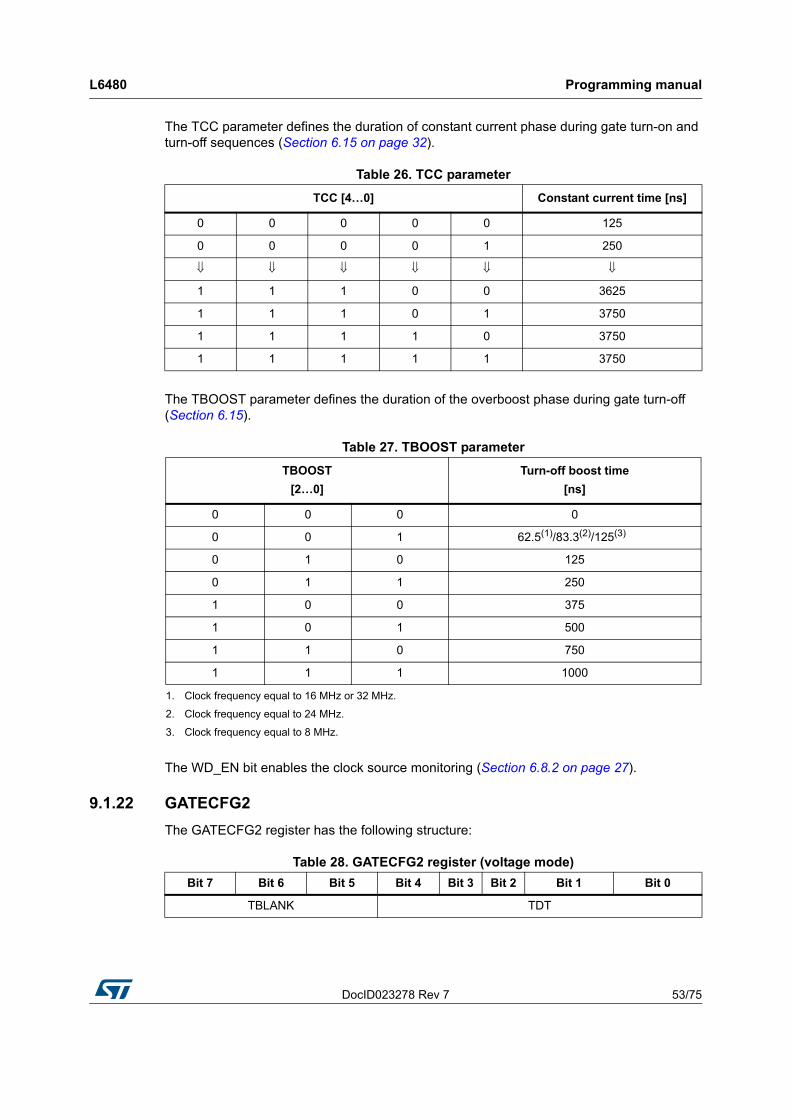
DocID023278 Rev 7 53/75
L6480 Programming manual
75
The TCC parameter defines the duration of constant current phase during gate turn-on and turn-off sequences (Section 6.15 on page 32).
The TBOOST parameter defines the duration of the overboost phase during gate turn-off (Section 6.15).
The WD_EN bit enables the clock source monitoring (Section 6.8.2 on page 27).
9.1.22 GATECFG2
The GATECFG2 register has the following structure:
Table 26. TCC parameter
TCC [4…0] Constant current time [ns]
0 0 0 0 0 125
0 0 0 0 1 250
1 1 1 0 0 3625
1 1 1 0 1 3750
1 1 1 1 0 3750
1 1 1 1 1 3750
Table 27. TBOOST parameter
TBOOST
[2…0]
Turn-off boost time
[ns]
0 0 0 0
0 0 1 62.5(1)/83.3(2)/125(3)
1. Clock frequency equal to 16 MHz or 32 MHz.
2. Clock frequency equal to 24 MHz.
3. Clock frequency equal to 8 MHz.
0 1 0 125
0 1 1 250
1 0 0 375
1 0 1 500
1 1 0 750
1 1 1 1000
Table 28. GATECFG2 register (voltage mode)
Bit 7 Bit 6 Bit 5 Bit 4 Bit 3 Bit 2 Bit 1 Bit 0
TBLANK TDT
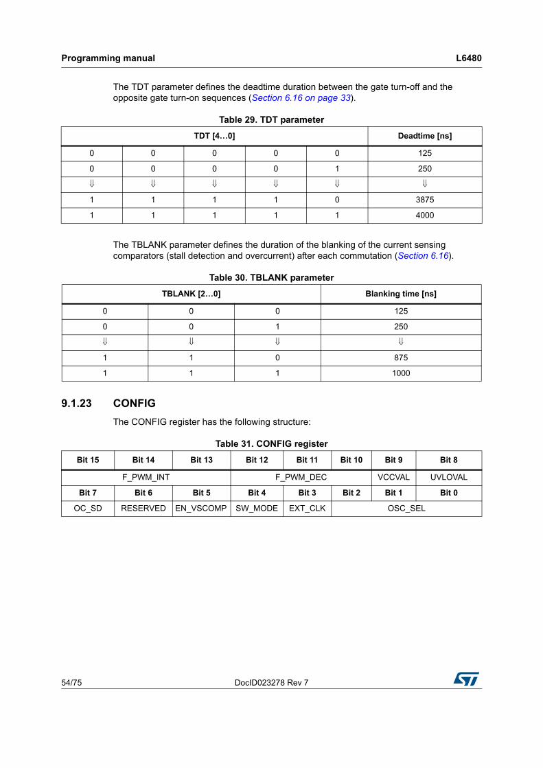
Programming manual L6480
54/75 DocID023278 Rev 7
The TDT parameter defines the deadtime duration between the gate turn-off and the opposite gate turn-on sequences (Section 6.16 on page 33).
The TBLANK parameter defines the duration of the blanking of the current sensing comparators (stall detection and overcurrent) after each commutation (Section 6.16).
9.1.23 CONFIG
The CONFIG register has the following structure:
Table 29. TDT parameter
TDT [4…0] Deadtime [ns]
0 0 0 0 0 125
0 0 0 0 1 250
1 1 1 1 0 3875
1 1 1 1 1 4000
Table 30. TBLANK parameter
TBLANK [2…0] Blanking time [ns]
0 0 0 125
0 0 1 250
1 1 0 875
1 1 1 1000
Table 31. CONFIG register
Bit 15 Bit 14 Bit 13 Bit 12 Bit 11 Bit 10 Bit 9 Bit 8
F_PWM_INT F_PWM_DEC VCCVAL UVLOVAL
Bit 7 Bit 6 Bit 5 Bit 4 Bit 3 Bit 2 Bit 1 Bit 0
OC_SD RESERVED EN_VSCOMP SW_MODE EXT_CLK OSC_SEL
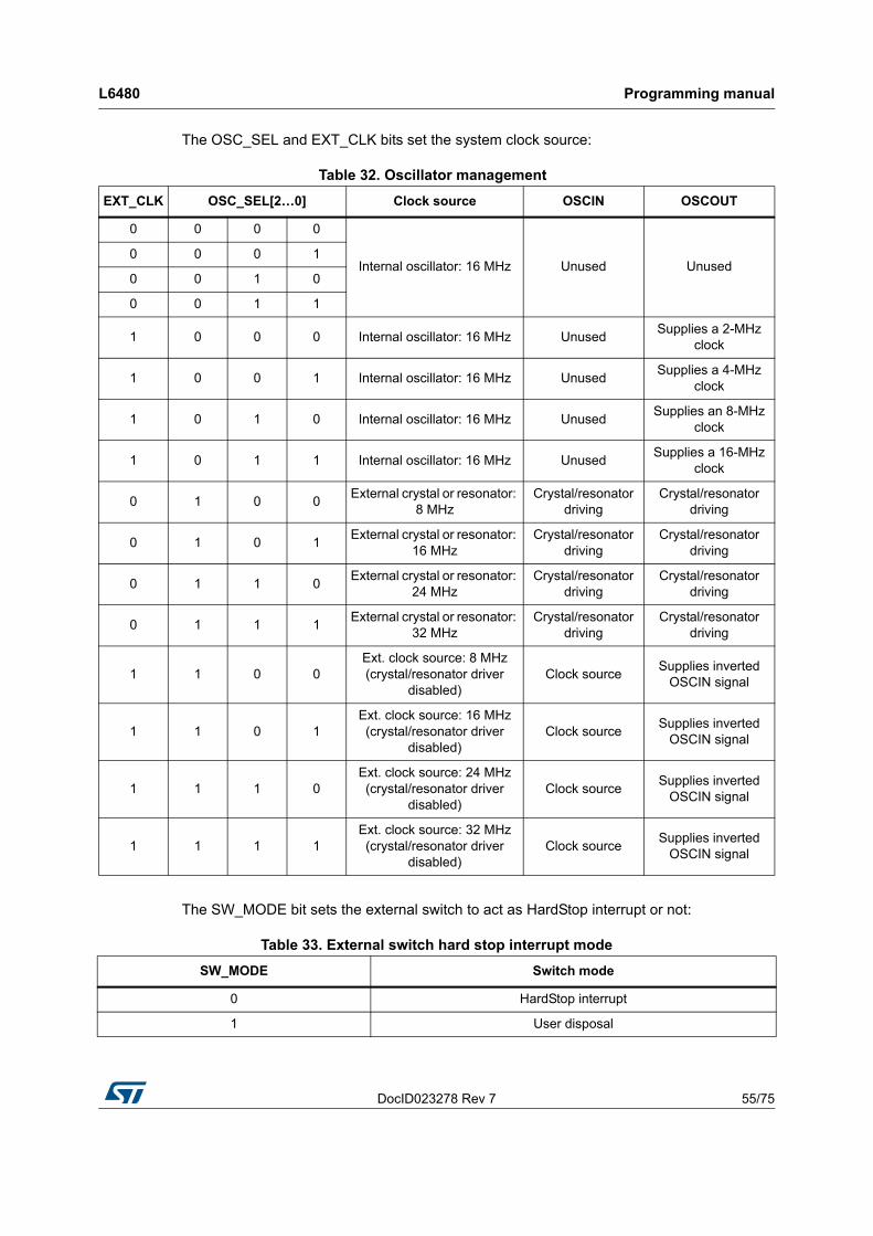
DocID023278 Rev 7 55/75
L6480 Programming manual
75
The OSC_SEL and EXT_CLK bits set the system clock source:
The SW_MODE bit sets the external switch to act as HardStop interrupt or not:
Table 32. Oscillator management
EXT_CLK OSC_SEL[2…0] Clock source OSCIN OSCOUT
0 0 0 0
Internal oscillator: 16 MHz Unused Unused0 0 0 1
0 0 1 0
0 0 1 1
1 0 0 0 Internal oscillator: 16 MHz UnusedSupplies a 2-MHz
clock
1 0 0 1 Internal oscillator: 16 MHz UnusedSupplies a 4-MHz
clock
1 0 1 0 Internal oscillator: 16 MHz UnusedSupplies an 8-MHz
clock
1 0 1 1 Internal oscillator: 16 MHz UnusedSupplies a 16-MHz
clock
0 1 0 0External crystal or resonator:
8 MHzCrystal/resonator
drivingCrystal/resonator
driving
0 1 0 1External crystal or resonator:
16 MHzCrystal/resonator
drivingCrystal/resonator
driving
0 1 1 0External crystal or resonator:
24 MHzCrystal/resonator
drivingCrystal/resonator
driving
0 1 1 1External crystal or resonator:
32 MHzCrystal/resonator
drivingCrystal/resonator
driving
1 1 0 0Ext. clock source: 8 MHz (crystal/resonator driver
disabled)Clock source
Supplies inverted OSCIN signal
1 1 0 1Ext. clock source: 16 MHz (crystal/resonator driver
disabled)Clock source
Supplies inverted OSCIN signal
1 1 1 0Ext. clock source: 24 MHz (crystal/resonator driver
disabled)Clock source
Supplies inverted OSCIN signal
1 1 1 1Ext. clock source: 32 MHz (crystal/resonator driver
disabled)Clock source
Supplies inverted OSCIN signal
Table 33. External switch hard stop interrupt mode
SW_MODE Switch mode
0 HardStop interrupt
1 User disposal
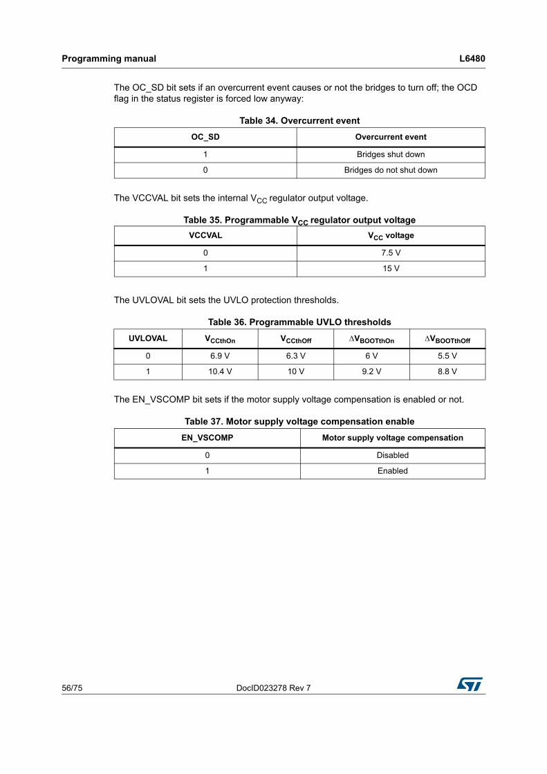
Programming manual L6480
56/75 DocID023278 Rev 7
The OC_SD bit sets if an overcurrent event causes or not the bridges to turn off; the OCD flag in the status register is forced low anyway:
The VCCVAL bit sets the internal VCC regulator output voltage.
Table 35. Programmable VCC regulator output voltage
The UVLOVAL bit sets the UVLO protection thresholds.
The EN_VSCOMP bit sets if the motor supply voltage compensation is enabled or not.
Table 34. Overcurrent event
OC_SD Overcurrent event
1 Bridges shut down
0 Bridges do not shut down
VCCVAL VCC voltage
0 7.5 V
1 15 V
Table 36. Programmable UVLO thresholds
UVLOVAL VCCthOn VCCthOff VBOOTthOn VBOOTthOff
0 6.9 V 6.3 V 6 V 5.5 V
1 10.4 V 10 V 9.2 V 8.8 V
Table 37. Motor supply voltage compensation enable
EN_VSCOMP Motor supply voltage compensation
0 Disabled
1 Enabled
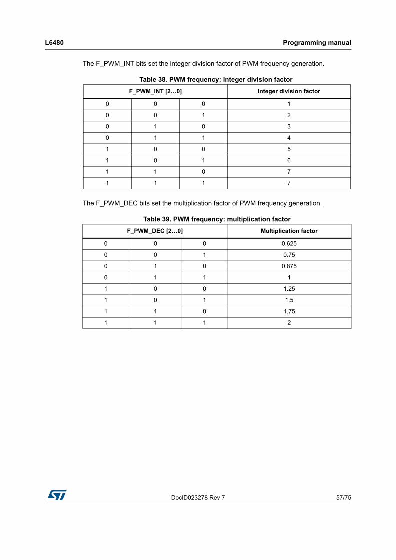
DocID023278 Rev 7 57/75
L6480 Programming manual
75
The F_PWM_INT bits set the integer division factor of PWM frequency generation.
The F_PWM_DEC bits set the multiplication factor of PWM frequency generation.
Table 38. PWM frequency: integer division factor
F_PWM_INT [2…0] Integer division factor
0 0 0 1
0 0 1 2
0 1 0 3
0 1 1 4
1 0 0 5
1 0 1 6
1 1 0 7
1 1 1 7
Table 39. PWM frequency: multiplication factor
F_PWM_DEC [2…0] Multiplication factor
0 0 0 0.625
0 0 1 0.75
0 1 0 0.875
0 1 1 1
1 0 0 1.25
1 0 1 1.5
1 1 0 1.75
1 1 1 2
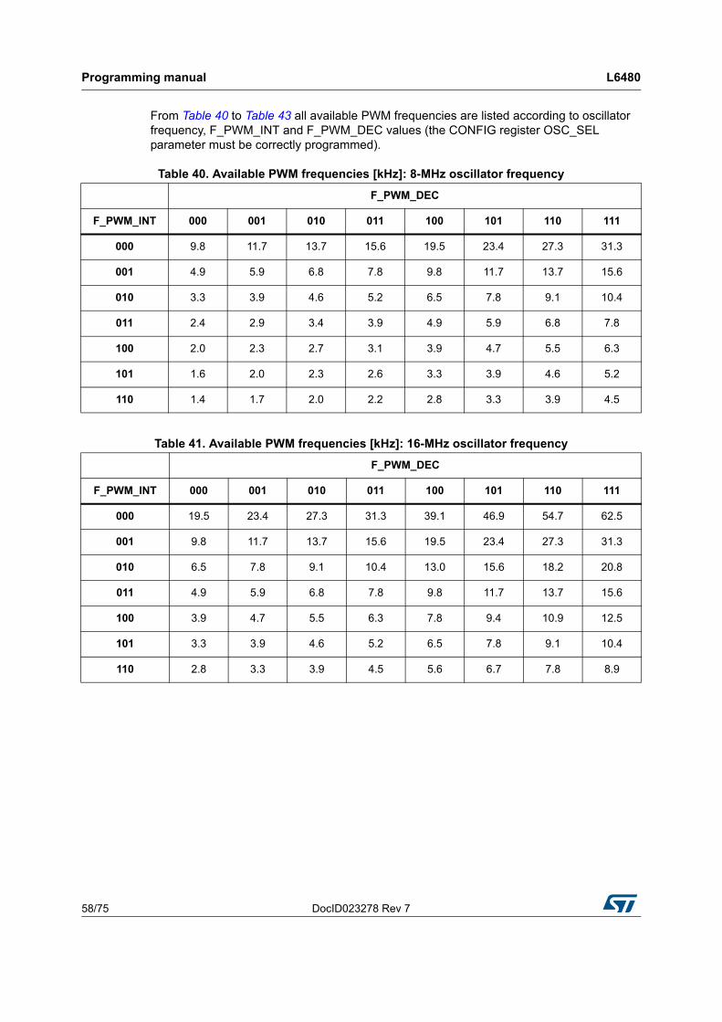
Programming manual L6480
58/75 DocID023278 Rev 7
From Table 40 to Table 43 all available PWM frequencies are listed according to oscillator frequency, F_PWM_INT and F_PWM_DEC values (the CONFIG register OSC_SEL parameter must be correctly programmed).
Table 40. Available PWM frequencies [kHz]: 8-MHz oscillator frequency
F_PWM_DEC
F_PWM_INT 000 001 010 011 100 101 110 111
000 9.8 11.7 13.7 15.6 19.5 23.4 27.3 31.3
001 4.9 5.9 6.8 7.8 9.8 11.7 13.7 15.6
010 3.3 3.9 4.6 5.2 6.5 7.8 9.1 10.4
011 2.4 2.9 3.4 3.9 4.9 5.9 6.8 7.8
100 2.0 2.3 2.7 3.1 3.9 4.7 5.5 6.3
101 1.6 2.0 2.3 2.6 3.3 3.9 4.6 5.2
110 1.4 1.7 2.0 2.2 2.8 3.3 3.9 4.5
Table 41. Available PWM frequencies [kHz]: 16-MHz oscillator frequency
F_PWM_DEC
F_PWM_INT 000 001 010 011 100 101 110 111
000 19.5 23.4 27.3 31.3 39.1 46.9 54.7 62.5
001 9.8 11.7 13.7 15.6 19.5 23.4 27.3 31.3
010 6.5 7.8 9.1 10.4 13.0 15.6 18.2 20.8
011 4.9 5.9 6.8 7.8 9.8 11.7 13.7 15.6
100 3.9 4.7 5.5 6.3 7.8 9.4 10.9 12.5
101 3.3 3.9 4.6 5.2 6.5 7.8 9.1 10.4
110 2.8 3.3 3.9 4.5 5.6 6.7 7.8 8.9
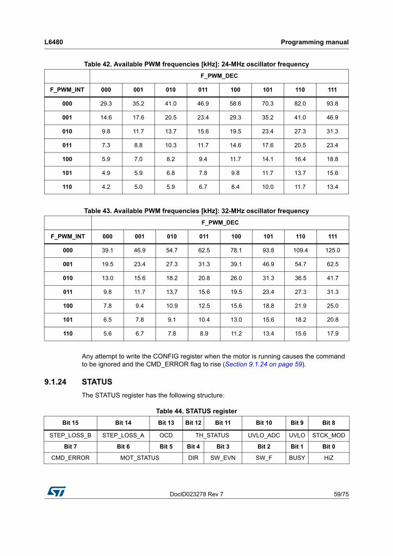
DocID023278 Rev 7 59/75
L6480 Programming manual
75
Any attempt to write the CONFIG register when the motor is running causes the command to be ignored and the CMD_ERROR flag to rise (Section 9.1.24 on page 59).
9.1.24 STATUS
The STATUS register has the following structure:
Table 42. Available PWM frequencies [kHz]: 24-MHz oscillator frequency
F_PWM_DEC
F_PWM_INT 000 001 010 011 100 101 110 111
000 29.3 35.2 41.0 46.9 58.6 70.3 82.0 93.8
001 14.6 17.6 20.5 23.4 29.3 35.2 41.0 46.9
010 9.8 11.7 13.7 15.6 19.5 23.4 27.3 31.3
011 7.3 8.8 10.3 11.7 14.6 17.6 20.5 23.4
100 5.9 7.0 8.2 9.4 11.7 14.1 16.4 18.8
101 4.9 5.9 6.8 7.8 9.8 11.7 13.7 15.6
110 4.2 5.0 5.9 6.7 8.4 10.0 11.7 13.4
Table 43. Available PWM frequencies [kHz]: 32-MHz oscillator frequency
F_PWM_DEC
F_PWM_INT 000 001 010 011 100 101 110 111
000 39.1 46.9 54.7 62.5 78.1 93.8 109.4 125.0
001 19.5 23.4 27.3 31.3 39.1 46.9 54.7 62.5
010 13.0 15.6 18.2 20.8 26.0 31.3 36.5 41.7
011 9.8 11.7 13.7 15.6 19.5 23.4 27.3 31.3
100 7.8 9.4 10.9 12.5 15.6 18.8 21.9 25.0
101 6.5 7.8 9.1 10.4 13.0 15.6 18.2 20.8
110 5.6 6.7 7.8 8.9 11.2 13.4 15.6 17.9
Table 44. STATUS register
Bit 15 Bit 14 Bit 13 Bit 12 Bit 11 Bit 10 Bit 9 Bit 8
STEP_LOSS_B STEP_LOSS_A OCD TH_STATUS UVLO_ADC UVLO STCK_MOD
Bit 7 Bit 6 Bit 5 Bit 4 Bit 3 Bit 2 Bit 1 Bit 0
CMD_ERROR MOT_STATUS DIR SW_EVN SW_F BUSY HiZ
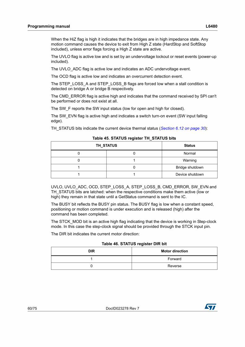
Programming manual L6480
60/75 DocID023278 Rev 7
When the HiZ flag is high it indicates that the bridges are in high impedance state. Any motion command causes the device to exit from High Z state (HardStop and SoftStop included), unless error flags forcing a High Z state are active.
The UVLO flag is active low and is set by an undervoltage lockout or reset events (power-up included).
The UVLO_ADC flag is active low and indicates an ADC undervoltage event.
The OCD flag is active low and indicates an overcurrent detection event.
The STEP_LOSS_A and STEP_LOSS_B flags are forced low when a stall condition is detected on bridge A or bridge B respectively.
The CMD_ERROR flag is active high and indicates that the command received by SPI can't be performed or does not exist at all.
The SW_F reports the SW input status (low for open and high for closed).
The SW_EVN flag is active high and indicates a switch turn-on event (SW input falling edge).
TH_STATUS bits indicate the current device thermal status (Section 6.12 on page 30):
UVLO, UVLO_ADC, OCD, STEP_LOSS_A, STEP_LOSS_B, CMD_ERROR, SW_EVN and TH_STATUS bits are latched: when the respective conditions make them active (low or high) they remain in that state until a GetStatus command is sent to the IC.
The BUSY bit reflects the BUSY pin status. The BUSY flag is low when a constant speed, positioning or motion command is under execution and is released (high) after the command has been completed.
The STCK_MOD bit is an active high flag indicating that the device is working in Step-clock mode. In this case the step-clock signal should be provided through the STCK input pin.
The DIR bit indicates the current motor direction:
Table 45. STATUS register TH_STATUS bits
TH_STATUS Status
0 0 Normal
0 1 Warning
1 0 Bridge shutdown
1 1 Device shutdown
Table 46. STATUS register DIR bit
DIR Motor direction
1 Forward
0 Reverse
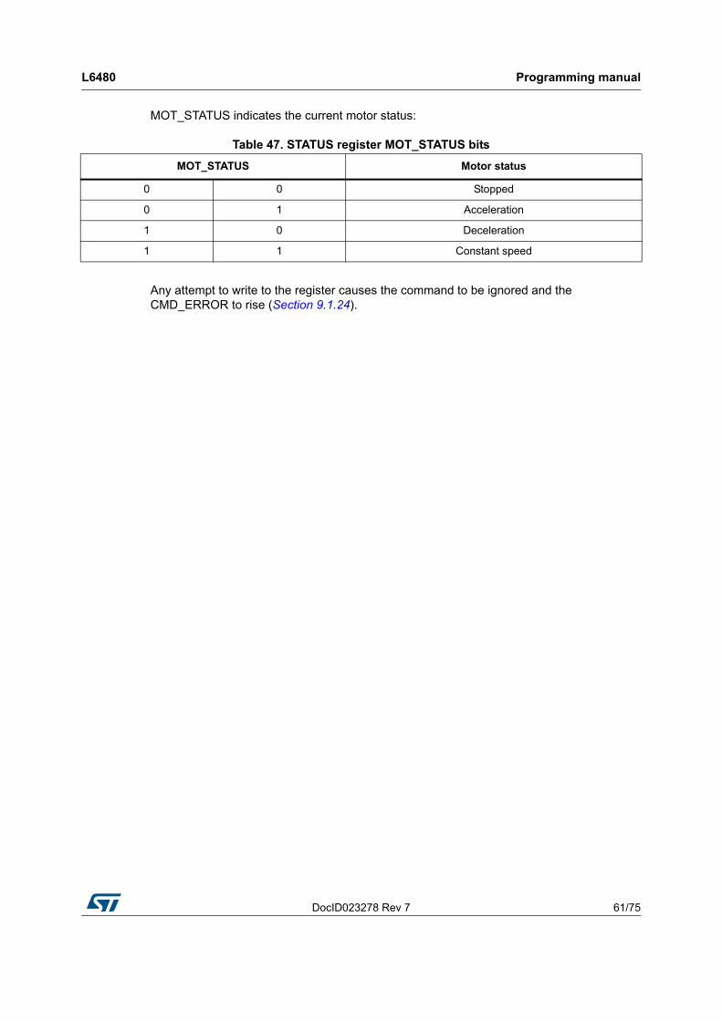
DocID023278 Rev 7 61/75
L6480 Programming manual
75
MOT_STATUS indicates the current motor status:
Any attempt to write to the register causes the command to be ignored and the CMD_ERROR to rise (Section 9.1.24).
Table 47. STATUS register MOT_STATUS bits
MOT_STATUS Motor status
0 0 Stopped
0 1 Acceleration
1 0 Deceleration
1 1 Constant speed
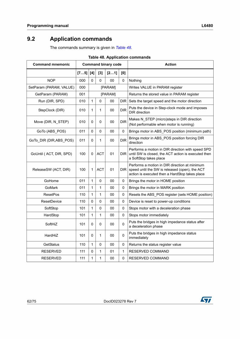
Programming manual L6480
62/75 DocID023278 Rev 7
9.2 Application commands
The commands summary is given in Table 48.
Table 48. Application commands
Command mnemonic Command binary code Action
[7…5] [4] [3] [2…1] [0]
NOP 000 0 0 00 0 Nothing
SetParam (PARAM, VALUE) 000 [PARAM] Writes VALUE in PARAM register
GetParam (PARAM) 001 [PARAM] Returns the stored value in PARAM register
Run (DIR, SPD) 010 1 0 00 DIR Sets the target speed and the motor direction
StepClock (DIR) 010 1 1 00 DIRPuts the device in Step-clock mode and imposes DIR direction
Move (DIR, N_STEP) 010 0 0 00 DIRMakes N_STEP (micro)steps in DIR direction
(Not performable when motor is running)
GoTo (ABS_POS) 011 0 0 00 0 Brings motor in ABS_POS position (minimum path)
GoTo_DIR (DIR,ABS_POS) 011 0 1 00 DIRBrings motor in ABS_POS position forcing DIR direction
GoUntil ( ACT, DIR, SPD) 100 0 ACT 01 DIRPerforms a motion in DIR direction with speed SPD until SW is closed, the ACT action is executed then a SoftStop takes place
ReleaseSW (ACT, DIR) 100 1 ACT 01 DIRPerforms a motion in DIR direction at minimum speed until the SW is released (open), the ACT action is executed then a HardStop takes place
GoHome 011 1 0 00 0 Brings the motor in HOME position
GoMark 011 1 1 00 0 Brings the motor in MARK position
ResetPos 110 1 1 00 0 Resets the ABS_POS register (sets HOME position)
ResetDevice 110 0 0 00 0 Device is reset to power-up conditions
SoftStop 101 1 0 00 0 Stops motor with a deceleration phase
HardStop 101 1 1 00 0 Stops motor immediately
SoftHiZ 101 0 0 00 0Puts the bridges in high impedance status after a deceleration phase
HardHiZ 101 0 1 00 0Puts the bridges in high impedance status immediately
GetStatus 110 1 0 00 0 Returns the status register value
RESERVED 111 0 1 01 1 RESERVED COMMAND
RESERVED 111 1 1 00 0 RESERVED COMMAND
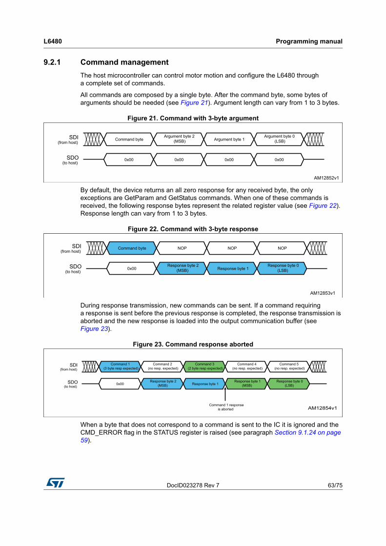
DocID023278 Rev 7 63/75
L6480 Programming manual
75
9.2.1 Command management
The host microcontroller can control motor motion and configure the L6480 through a complete set of commands.
All commands are composed by a single byte. After the command byte, some bytes of arguments should be needed (see Figure 21). Argument length can vary from 1 to 3 bytes.
Figure 21. Command with 3-byte argument
By default, the device returns an all zero response for any received byte, the only exceptions are GetParam and GetStatus commands. When one of these commands is received, the following response bytes represent the related register value (see Figure 22). Response length can vary from 1 to 3 bytes.
Figure 22. Command with 3-byte response
During response transmission, new commands can be sent. If a command requiring a response is sent before the previous response is completed, the response transmission is aborted and the new response is loaded into the output communication buffer (see Figure 23).
Figure 23. Command response aborted
When a byte that does not correspond to a command is sent to the IC it is ignored and the CMD_ERROR flag in the STATUS register is raised (see paragraph Section 9.1.24 on page 59).
Programming manual L6480
64/75 DocID023278 Rev 7
9.2.2 Nop
Nothing is performed.
9.2.3 SetParam (PARAM, VALUE)
The SetParam command sets the PARAM register value equal to VALUE; PARAM is the respective register address listed in Table 11 on page 43.
The command should be followed by the new register VALUE (most significant byte first). The number of bytes composing the VALUE argument depends on the length of the target register (see Table 11).
Some registers cannot be written (see Table 11); any attempt to write one of those registers causes the command to be ignored and the CMD_ERROR flag to rise at the end of the command byte, as if an unknown command code were sent (see Section 9.1.24 on page 59).
Some registers can only be written in particular conditions (see Table 11); any attempt to write one of those registers when the conditions are not satisfied causes the command to be ignored and the CMD_ERROR flag to rise at the end of the last argument byte (see Section 9.1.24).
Any attempt to set an inexistent register (wrong address value) causes the command to be ignored and the CMD_ERROR flag to rise at the end of the command byte as if an unknown command code were sent.
9.2.4 GetParam (PARAM)
Table 49. Nop command structure
Bit 7 Bit 6 Bit 5 Bit 4 Bit 3 Bit 2 Bit 1 Bit 0
0 0 0 0 0 0 0 0 From host
Table 50. SetParam command structure
Bit 7 Bit 6 Bit 5 Bit 4 Bit 3 Bit 2 Bit 1 Bit 0
0 0 0 PARAM
From hostVALUE Byte 2 (if needed)
VALUE Byte 1 (if needed)
VALUE Byte 0
Table 51. GetParam command structure
Bit 7 Bit 6 Bit 5 Bit 4 Bit 3 Bit 2 Bit 1 Bit 0
0 0 1 PARAM From host
ANS Byte 2 (if needed) To host
ANS Byte 1 (if needed) To host
ANS Byte 0 To host
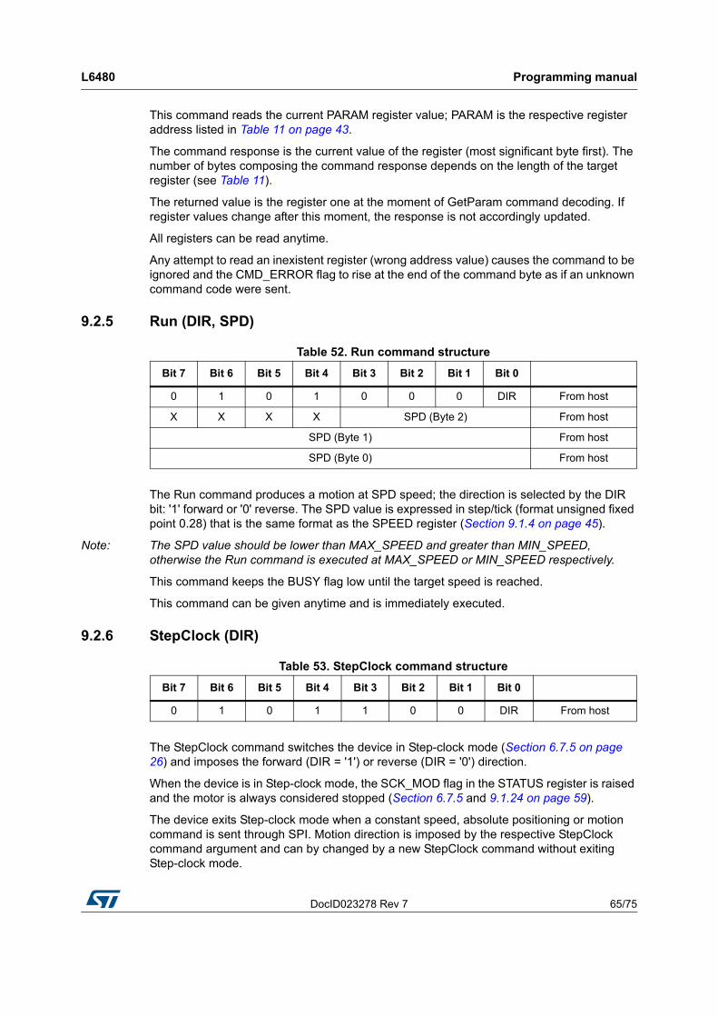
DocID023278 Rev 7 65/75
L6480 Programming manual
75
This command reads the current PARAM register value; PARAM is the respective register address listed in Table 11 on page 43.
The command response is the current value of the register (most significant byte first). The number of bytes composing the command response depends on the length of the target register (see Table 11).
The returned value is the register one at the moment of GetParam command decoding. If register values change after this moment, the response is not accordingly updated.
All registers can be read anytime.
Any attempt to read an inexistent register (wrong address value) causes the command to be ignored and the CMD_ERROR flag to rise at the end of the command byte as if an unknown command code were sent.
9.2.5 Run (DIR, SPD)
The Run command produces a motion at SPD speed; the direction is selected by the DIR bit: '1' forward or '0' reverse. The SPD value is expressed in step/tick (format unsigned fixed point 0.28) that is the same format as the SPEED register (Section 9.1.4 on page 45).
Note: The SPD value should be lower than MAX_SPEED and greater than MIN_SPEED, otherwise the Run command is executed at MAX_SPEED or MIN_SPEED respectively.
This command keeps the BUSY flag low until the target speed is reached.
This command can be given anytime and is immediately executed.
9.2.6 StepClock (DIR)
The StepClock command switches the device in Step-clock mode (Section 6.7.5 on page 26) and imposes the forward (DIR = '1') or reverse (DIR = '0') direction.
When the device is in Step-clock mode, the SCK_MOD flag in the STATUS register is raised and the motor is always considered stopped (Section 6.7.5 and 9.1.24 on page 59).
The device exits Step-clock mode when a constant speed, absolute positioning or motion command is sent through SPI. Motion direction is imposed by the respective StepClock command argument and can by changed by a new StepClock command without exiting Step-clock mode.
Table 52. Run command structure
Bit 7 Bit 6 Bit 5 Bit 4 Bit 3 Bit 2 Bit 1 Bit 0
0 1 0 1 0 0 0 DIR From host
X X X X SPD (Byte 2) From host
SPD (Byte 1) From host
SPD (Byte 0) From host
Table 53. StepClock command structure
Bit 7 Bit 6 Bit 5 Bit 4 Bit 3 Bit 2 Bit 1 Bit 0
0 1 0 1 1 0 0 DIR From host
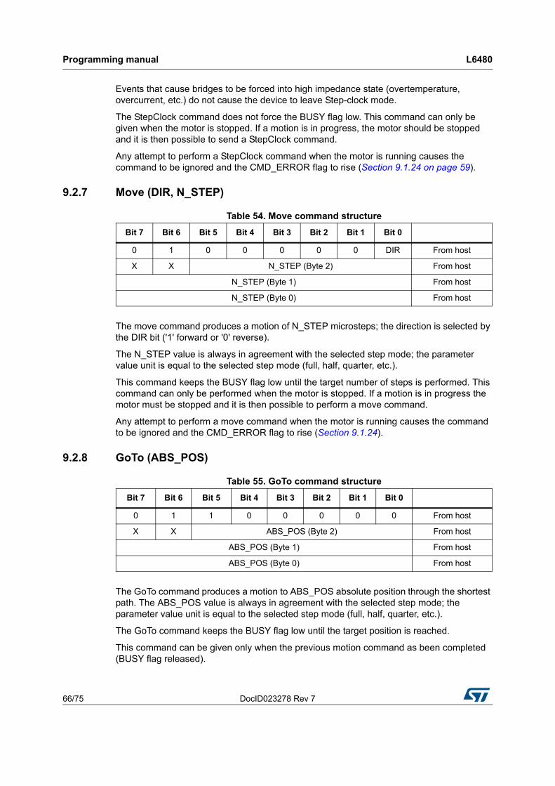
Programming manual L6480
66/75 DocID023278 Rev 7
Events that cause bridges to be forced into high impedance state (overtemperature, overcurrent, etc.) do not cause the device to leave Step-clock mode.
The StepClock command does not force the BUSY flag low. This command can only be given when the motor is stopped. If a motion is in progress, the motor should be stopped and it is then possible to send a StepClock command.
Any attempt to perform a StepClock command when the motor is running causes the command to be ignored and the CMD_ERROR flag to rise (Section 9.1.24 on page 59).
9.2.7 Move (DIR, N_STEP)
The move command produces a motion of N_STEP microsteps; the direction is selected by the DIR bit ('1' forward or '0' reverse).
The N_STEP value is always in agreement with the selected step mode; the parameter value unit is equal to the selected step mode (full, half, quarter, etc.).
This command keeps the BUSY flag low until the target number of steps is performed. This command can only be performed when the motor is stopped. If a motion is in progress the motor must be stopped and it is then possible to perform a move command.
Any attempt to perform a move command when the motor is running causes the command to be ignored and the CMD_ERROR flag to rise (Section 9.1.24).
9.2.8 GoTo (ABS_POS)
The GoTo command produces a motion to ABS_POS absolute position through the shortest path. The ABS_POS value is always in agreement with the selected step mode; the parameter value unit is equal to the selected step mode (full, half, quarter, etc.).
The GoTo command keeps the BUSY flag low until the target position is reached.
This command can be given only when the previous motion command as been completed (BUSY flag released).
Table 54. Move command structure
Bit 7 Bit 6 Bit 5 Bit 4 Bit 3 Bit 2 Bit 1 Bit 0
0 1 0 0 0 0 0 DIR From host
X X N_STEP (Byte 2) From host
N_STEP (Byte 1) From host
N_STEP (Byte 0) From host
Table 55. GoTo command structure
Bit 7 Bit 6 Bit 5 Bit 4 Bit 3 Bit 2 Bit 1 Bit 0
0 1 1 0 0 0 0 0 From host
X X ABS_POS (Byte 2) From host
ABS_POS (Byte 1) From host
ABS_POS (Byte 0) From host
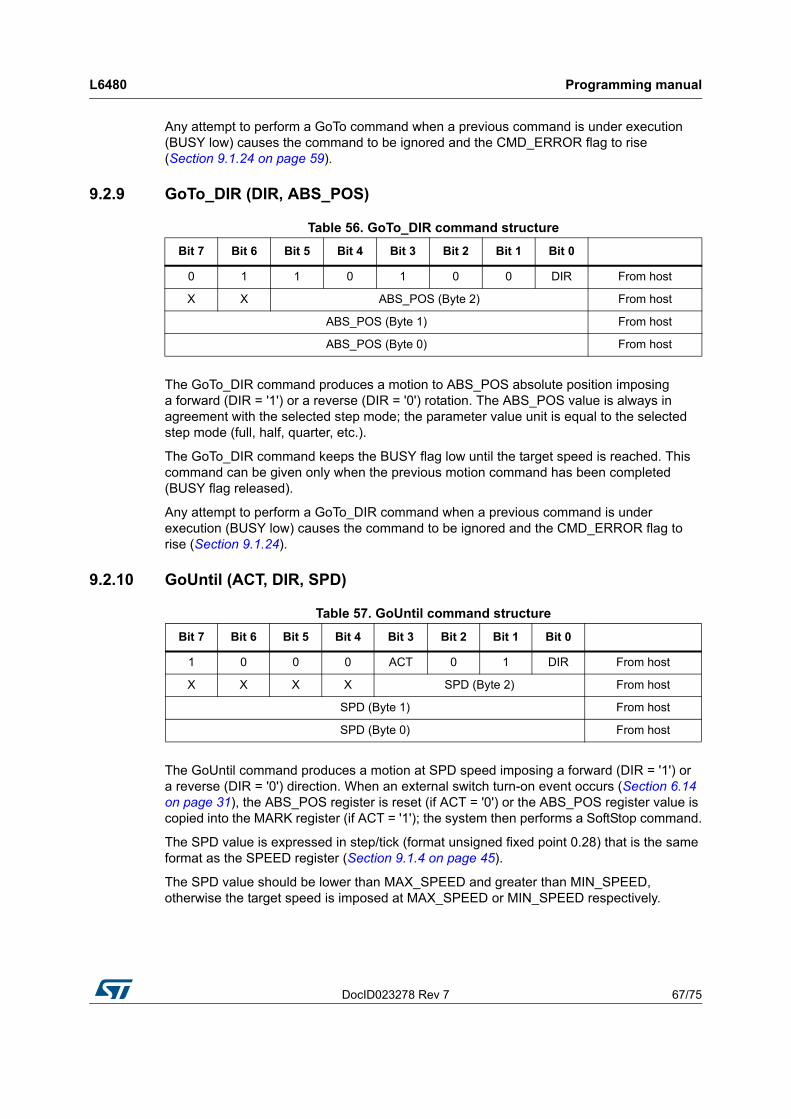
DocID023278 Rev 7 67/75
L6480 Programming manual
75
Any attempt to perform a GoTo command when a previous command is under execution (BUSY low) causes the command to be ignored and the CMD_ERROR flag to rise (Section 9.1.24 on page 59).
9.2.9 GoTo_DIR (DIR, ABS_POS)
The GoTo_DIR command produces a motion to ABS_POS absolute position imposing a forward (DIR = '1') or a reverse (DIR = '0') rotation. The ABS_POS value is always in agreement with the selected step mode; the parameter value unit is equal to the selected step mode (full, half, quarter, etc.).
The GoTo_DIR command keeps the BUSY flag low until the target speed is reached. This command can be given only when the previous motion command has been completed (BUSY flag released).
Any attempt to perform a GoTo_DIR command when a previous command is under execution (BUSY low) causes the command to be ignored and the CMD_ERROR flag to rise (Section 9.1.24).
9.2.10 GoUntil (ACT, DIR, SPD)
The GoUntil command produces a motion at SPD speed imposing a forward (DIR = '1') or a reverse (DIR = '0') direction. When an external switch turn-on event occurs (Section 6.14 on page 31), the ABS_POS register is reset (if ACT = '0') or the ABS_POS register value is copied into the MARK register (if ACT = '1'); the system then performs a SoftStop command.
The SPD value is expressed in step/tick (format unsigned fixed point 0.28) that is the same format as the SPEED register (Section 9.1.4 on page 45).
The SPD value should be lower than MAX_SPEED and greater than MIN_SPEED, otherwise the target speed is imposed at MAX_SPEED or MIN_SPEED respectively.
Table 56. GoTo_DIR command structure
Bit 7 Bit 6 Bit 5 Bit 4 Bit 3 Bit 2 Bit 1 Bit 0
0 1 1 0 1 0 0 DIR From host
X X ABS_POS (Byte 2) From host
ABS_POS (Byte 1) From host
ABS_POS (Byte 0) From host
Table 57. GoUntil command structure
Bit 7 Bit 6 Bit 5 Bit 4 Bit 3 Bit 2 Bit 1 Bit 0
1 0 0 0 ACT 0 1 DIR From host
X X X X SPD (Byte 2) From host
SPD (Byte 1) From host
SPD (Byte 0) From host
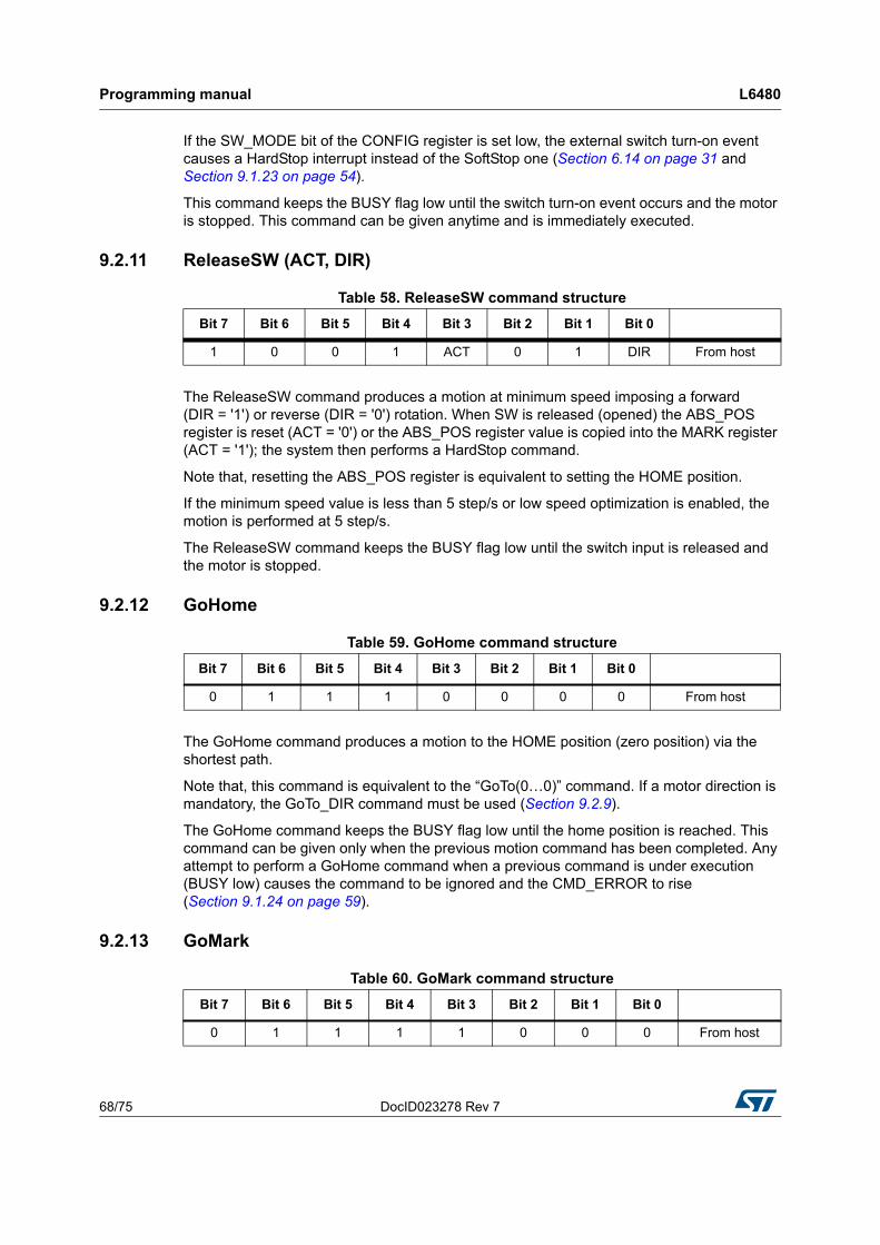
Programming manual L6480
68/75 DocID023278 Rev 7
If the SW_MODE bit of the CONFIG register is set low, the external switch turn-on event causes a HardStop interrupt instead of the SoftStop one (Section 6.14 on page 31 and Section 9.1.23 on page 54).
This command keeps the BUSY flag low until the switch turn-on event occurs and the motor is stopped. This command can be given anytime and is immediately executed.
9.2.11 ReleaseSW (ACT, DIR)
The ReleaseSW command produces a motion at minimum speed imposing a forward (DIR = '1') or reverse (DIR = '0') rotation. When SW is released (opened) the ABS_POS register is reset (ACT = '0') or the ABS_POS register value is copied into the MARK register (ACT = '1'); the system then performs a HardStop command.
Note that, resetting the ABS_POS register is equivalent to setting the HOME position.
If the minimum speed value is less than 5 step/s or low speed optimization is enabled, the motion is performed at 5 step/s.
The ReleaseSW command keeps the BUSY flag low until the switch input is released and the motor is stopped.
9.2.12 GoHome
The GoHome command produces a motion to the HOME position (zero position) via the shortest path.
Note that, this command is equivalent to the “GoTo(0…0)” command. If a motor direction is mandatory, the GoTo_DIR command must be used (Section 9.2.9).
The GoHome command keeps the BUSY flag low until the home position is reached. This command can be given only when the previous motion command has been completed. Any attempt to perform a GoHome command when a previous command is under execution (BUSY low) causes the command to be ignored and the CMD_ERROR to rise (Section 9.1.24 on page 59).
9.2.13 GoMark
Table 58. ReleaseSW command structure
Bit 7 Bit 6 Bit 5 Bit 4 Bit 3 Bit 2 Bit 1 Bit 0
1 0 0 1 ACT 0 1 DIR From host
Table 59. GoHome command structure
Bit 7 Bit 6 Bit 5 Bit 4 Bit 3 Bit 2 Bit 1 Bit 0
0 1 1 1 0 0 0 0 From host
Table 60. GoMark command structure
Bit 7 Bit 6 Bit 5 Bit 4 Bit 3 Bit 2 Bit 1 Bit 0
0 1 1 1 1 0 0 0 From host
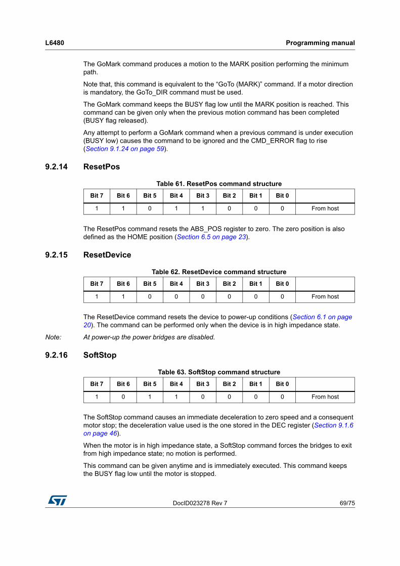
DocID023278 Rev 7 69/75
L6480 Programming manual
75
The GoMark command produces a motion to the MARK position performing the minimum path.
Note that, this command is equivalent to the “GoTo (MARK)” command. If a motor direction is mandatory, the GoTo_DIR command must be used.
The GoMark command keeps the BUSY flag low until the MARK position is reached. This command can be given only when the previous motion command has been completed (BUSY flag released).
Any attempt to perform a GoMark command when a previous command is under execution (BUSY low) causes the command to be ignored and the CMD_ERROR flag to rise (Section 9.1.24 on page 59).
9.2.14 ResetPos
The ResetPos command resets the ABS_POS register to zero. The zero position is also defined as the HOME position (Section 6.5 on page 23).
9.2.15 ResetDevice
The ResetDevice command resets the device to power-up conditions (Section 6.1 on page 20). The command can be performed only when the device is in high impedance state.
Note: At power-up the power bridges are disabled.
9.2.16 SoftStop
The SoftStop command causes an immediate deceleration to zero speed and a consequent motor stop; the deceleration value used is the one stored in the DEC register (Section 9.1.6 on page 46).
When the motor is in high impedance state, a SoftStop command forces the bridges to exit from high impedance state; no motion is performed.
This command can be given anytime and is immediately executed. This command keeps the BUSY flag low until the motor is stopped.
Table 61. ResetPos command structure
Bit 7 Bit 6 Bit 5 Bit 4 Bit 3 Bit 2 Bit 1 Bit 0
1 1 0 1 1 0 0 0 From host
Table 62. ResetDevice command structure
Bit 7 Bit 6 Bit 5 Bit 4 Bit 3 Bit 2 Bit 1 Bit 0
1 1 0 0 0 0 0 0 From host
Table 63. SoftStop command structure
Bit 7 Bit 6 Bit 5 Bit 4 Bit 3 Bit 2 Bit 1 Bit 0
1 0 1 1 0 0 0 0 From host
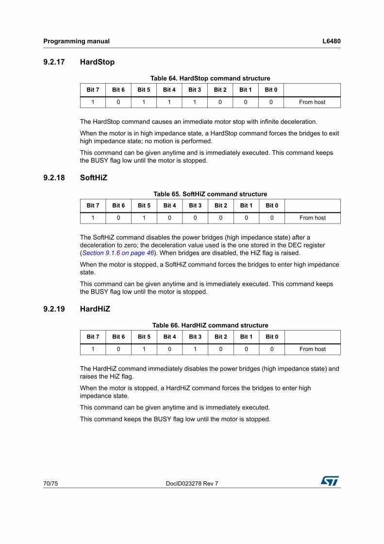
Programming manual L6480
70/75 DocID023278 Rev 7
9.2.17 HardStop
The HardStop command causes an immediate motor stop with infinite deceleration.
When the motor is in high impedance state, a HardStop command forces the bridges to exit high impedance state; no motion is performed.
This command can be given anytime and is immediately executed. This command keeps the BUSY flag low until the motor is stopped.
9.2.18 SoftHiZ
The SoftHiZ command disables the power bridges (high impedance state) after a deceleration to zero; the deceleration value used is the one stored in the DEC register (Section 9.1.6 on page 46). When bridges are disabled, the HiZ flag is raised.
When the motor is stopped, a SoftHiZ command forces the bridges to enter high impedance state.
This command can be given anytime and is immediately executed. This command keeps the BUSY flag low until the motor is stopped.
9.2.19 HardHiZ
The HardHiZ command immediately disables the power bridges (high impedance state) and raises the HiZ flag.
When the motor is stopped, a HardHiZ command forces the bridges to enter high impedance state.
This command can be given anytime and is immediately executed.
This command keeps the BUSY flag low until the motor is stopped.
Table 64. HardStop command structure
Bit 7 Bit 6 Bit 5 Bit 4 Bit 3 Bit 2 Bit 1 Bit 0
1 0 1 1 1 0 0 0 From host
Table 65. SoftHiZ command structure
Bit 7 Bit 6 Bit 5 Bit 4 Bit 3 Bit 2 Bit 1 Bit 0
1 0 1 0 0 0 0 0 From host
Table 66. HardHiZ command structure
Bit 7 Bit 6 Bit 5 Bit 4 Bit 3 Bit 2 Bit 1 Bit 0
1 0 1 0 1 0 0 0 From host
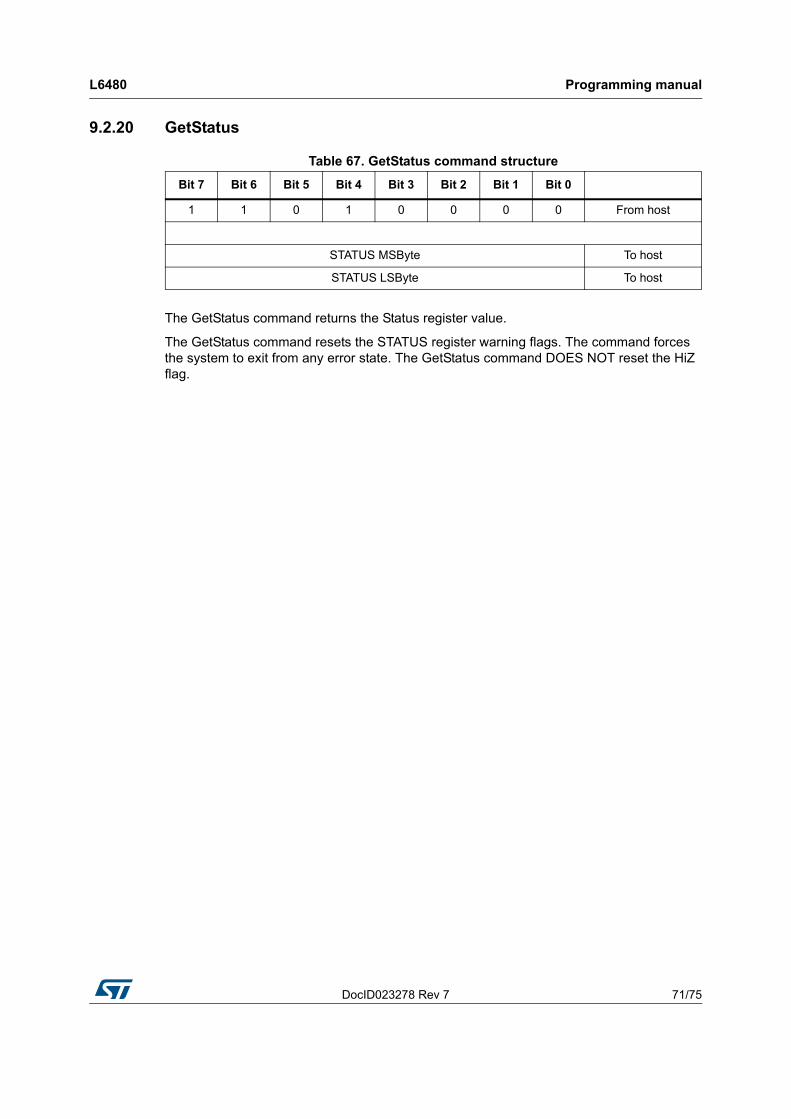
DocID023278 Rev 7 71/75
L6480 Programming manual
75
9.2.20 GetStatus
The GetStatus command returns the Status register value.
The GetStatus command resets the STATUS register warning flags. The command forces the system to exit from any error state. The GetStatus command DOES NOT reset the HiZ flag.
Table 67. GetStatus command structure
Bit 7 Bit 6 Bit 5 Bit 4 Bit 3 Bit 2 Bit 1 Bit 0
1 1 0 1 0 0 0 0 From host
STATUS MSByte To host
STATUS LSByte To host
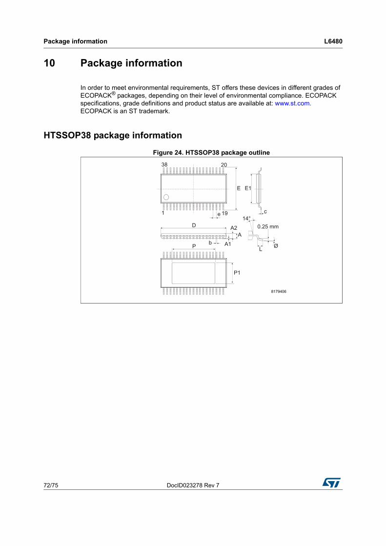
Package information L6480
72/75 DocID023278 Rev 7
10 Package information
In order to meet environmental requirements, ST offers these devices in different grades of ECOPACK® packages, depending on their level of environmental compliance. ECOPACK specifications, grade definitions and product status are available at: www.st.com. ECOPACK is an ST trademark.
HTSSOP38 package information
Figure 24. HTSSOP38 package outline
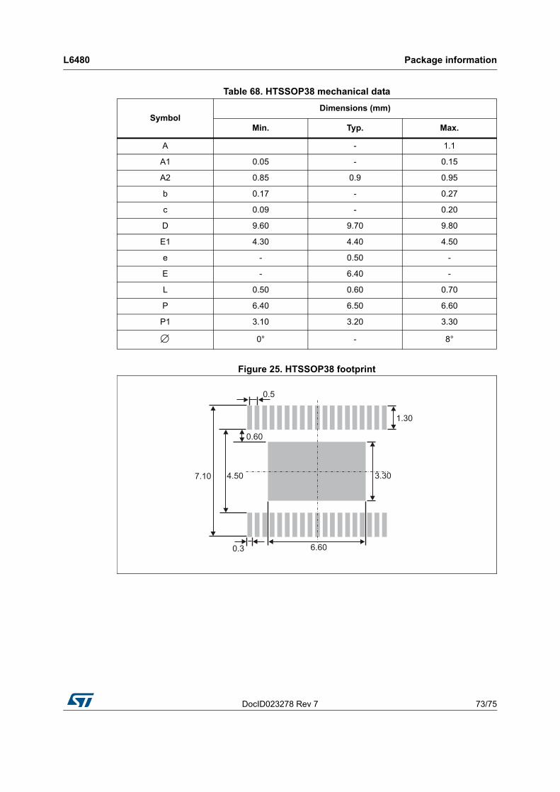
DocID023278 Rev 7 73/75
L6480 Package information
75
Figure 25. HTSSOP38 footprint
Table 68. HTSSOP38 mechanical data
SymbolDimensions (mm)
Min. Typ. Max.
A - 1.1
A1 0.05 - 0.15
A2 0.85 0.9 0.95
b 0.17 - 0.27
c 0.09 - 0.20
D 9.60 9.70 9.80
E1 4.30 4.40 4.50
e - 0.50 -
E - 6.40 -
L 0.50 0.60 0.70
P 6.40 6.50 6.60
P1 3.10 3.20 3.30
0° - 8°
Revision history L6480
74/75 DocID023278 Rev 7
11 Revision history
FLAG output
Table 69. Document revision history
Date Revision Changes
13-Jun-2012 1 Initial release.
04-Oct-2012 2
Updated Table 2, Table 5, Table 6, Table 9, Table 31, Table 36.
Update Figure 8, Figure 9, Figure 10.
Minor text changes.
19-Dec-2012 3
Changed the title.
Inserted footnote in Table 2 and in Table 4.
Updated Table 18 and Table 19.
12-Dec-2013 4
Updated Section 6.3, (replaced “integrated MOSFETs” by “gate drivers”).
Updated Section 6.9 to Section 6.13, Section 7.2 (replaced “gates” by “MOSFETs”).
Added cross-references to Section 9.
Updated Section 9.1.22 (replaced “TCC parameter” by “TDT parameter”).
Updated Section 9.2.15 (Added “The command can be performed only when the device is in high impedance state”).
Updated Section 10 (reversed order of Figure 24 and Table 68, updated titles).
Minor modifications throughout document.
19-May-2014 5
Updated Table 2 on page 10 [added (VBOOT - VS) to VBOOT].
Updated Table 5 on page 12 (updated values of thigh,STCK, tlow,STCK, and thigh).
Updated Table 7 on page 19 (replaced STD25NF10 by STD25N10F7).
Updated Section 6.1 on page 20 (removed VCC and VBOOT, added FLAG output...).
Updated Section 6.4 on page 21 (replaced “the first microstep” by “zero”).
Replaced NOTPERF_CMD and WRONG_CMD flag by CMD_ERROR flag throughout document.
Updated Section 9.1.5 on page 45 (replaced sentence: “When the ACC value is set to 0xFFF, the device works in infinite acceleration mode.” by “The 0xFFF value of the register is reserved and it should never be used.”).
Updated Section 9.1.6 on page 46 (removed sentence: “When the device is working in infinite acceleration mode this value is ignored.”).
Updated Table 44 on page 59 (replaced TH_SD by TH_STATUS).
Updated title of Table 47 on page 61 (replaced MOT_STATE by MOT_STATUS).
Updated cross-references throughout document.
05-Mar-2015 6Updated main title on page 1 (removed cSPIN™).
Updated Table 11 on page 43 (h15 - Len. [bit]: replaced 10 by 11).
23-Mar-2015 7Updated Table 14 on page 47 (“Bit 11” removed).
Minor modifications throughout document.
DocID023278 Rev 7 75/75
L6480
75
IMPORTANT NOTICE – PLEASE READ CAREFULLY
STMicroelectronics NV and its subsidiaries (“ST”) reserve the right to make changes, corrections, enhancements, modifications, and improvements to ST products and/or to this document at any time without notice. Purchasers should obtain the latest relevant information on ST products before placing orders. ST products are sold pursuant to ST’s terms and conditions of sale in place at the time of order acknowledgement.
Purchasers are solely responsible for the choice, selection, and use of ST products and ST assumes no liability for application assistance or the design of Purchasers’ products.
No license, express or implied, to any intellectual property right is granted by ST herein.
Resale of ST products with provisions different from the information set forth herein shall void any warranty granted by ST for such product.
ST and the ST logo are trademarks of ST. All other product or service names are the property of their respective owners.
Information in this document supersedes and replaces information previously supplied in any prior versions of this document.
© 2015 STMicroelectronics – All rights reserved