Microscopic Light-Beam Induced Current Measurement for High … · 2018-01-08 · Microscopic...
17
© Fraunhofer-Center für Silizium-Photovoltaik CSP Microscopic Light-Beam Induced Current Measurement for High-Resolution Solar Cell Characterization Susanne Richter, Stephan Großer, Tabea Luka, Marko Turek, Martina Werner, Christian Hagendorf Fraunhofer Center for Silicon Photovoltaics CSP Otto-Eißfeldt-St. 12 06120 Halle (Saale) [email protected] 28.09.2016
Transcript of Microscopic Light-Beam Induced Current Measurement for High … · 2018-01-08 · Microscopic...

© Fraunhofer-Center für Silizium-Photovoltaik CSP
Microscopic Light-Beam Induced Current Measurement for High-Resolution Solar Cell Characterization
Susanne Richter, Stephan Großer, Tabea Luka, Marko Turek, Martina Werner, Christian Hagendorf
Fraunhofer Center for Silicon Photovoltaics CSP Otto-Eißfeldt-St. 12 06120 Halle (Saale) [email protected]
28.09.2016

© Fraunhofer-Center für Silizium-Photovoltaik CSP
Content
Motivation
Principle of µLBIC
Results of new devloped application
Comparison of EBIC and µLBIC measurements
Correlative LBIC measurements from macroscopic to microscopic scale
Conclusion

© Fraunhofer-Center für Silizium-Photovoltaik CSP
Motivation
Quality control from module to cell level Non-destructive failure analysis, inline diagnostics on module and cell level
Information of local structural, optical and electrical properties needed
Current systems of electrical characterization on solar cell level limited in spatial resolution
correlation between structural and electrical properties
Separate measurement of 2D photo current images and topography and/or light microscopic images
Non-destructive investigation of degradation mechanism
Alternative method to EBIC
EL
© Fraunhofer-Center für Silizium-Photovoltaik CSP
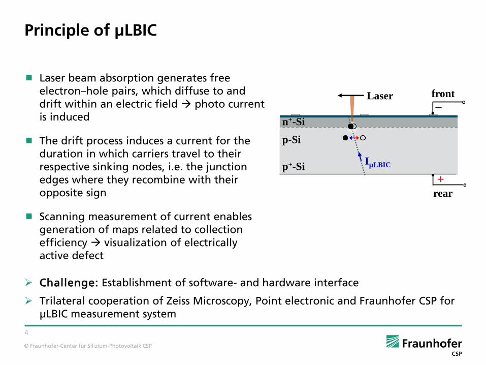
Principle of µLBIC Laser beam absorption generates free
electron–hole pairs, which diffuse to and drift within an electric field photo current is induced
The drift process induces a current for the duration in which carriers travel to their respective sinking nodes, i.e. the junction edges where they recombine with their opposite sign
Scanning measurement of current enables generation of maps related to collection efficiency visualization of electrically active defect
n+-Si
p-Si
p+-Si IµLBIC
+
– front
rear
Laser
Challenge: Establishment of software- and hardware interface
Trilateral cooperation of Zeiss Microscopy, Point electronic and Fraunhofer CSP for µLBIC measurement system

© Fraunhofer-Center für Silizium-Photovoltaik CSP
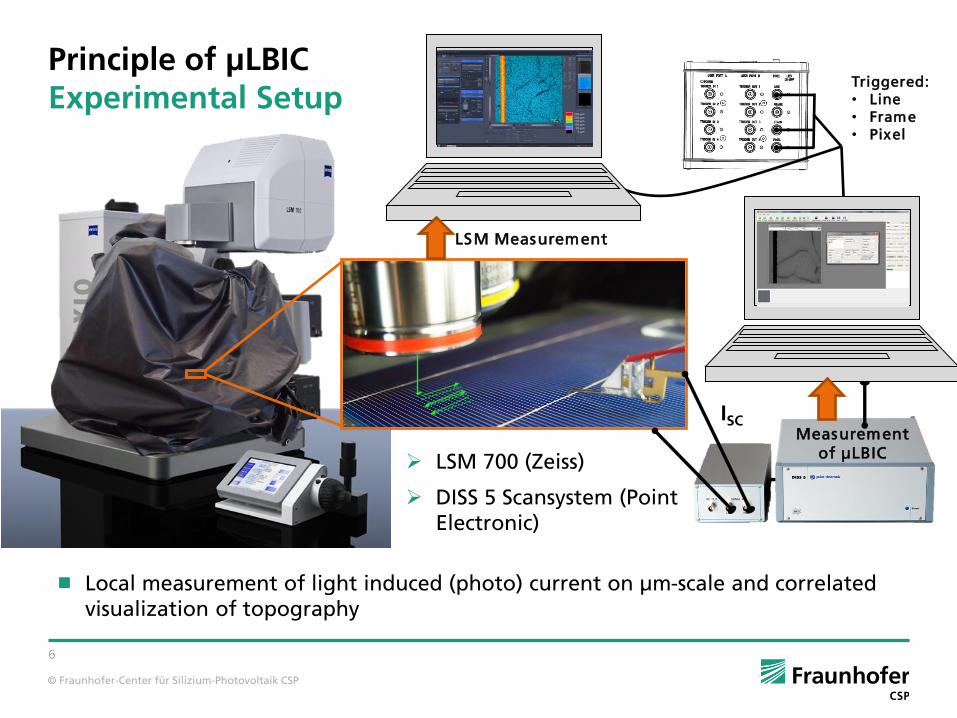
Principle of µLBIC Experimental Setup
Local measurement of light induced (photo) current on µm-scale and correlated visualization of topography
LSM 700 (Zeiss)
DISS 5 Scansystem (Point Electronic)
© Fraunhofer-Center für Silizium-Photovoltaik CSP
Principle of µLBIC Experimental Setup
Local measurement of light induced (photo) current on µm-scale and correlated visualization of topography
LSM 700 (Zeiss)
DISS 5 Scansystem (Point Electronic)
Measurement of µLBIC
ISC
LSM Measurement
Triggered: • Line • Frame • Pixel

© Fraunhofer-Center für Silizium-Photovoltaik CSP
405 nm
555 nm
639 nm
Physical background - absorption depth
Absorption depth (1/α) corresponds to intensity drop of 1/e (~36%)
Choice of wavelength influences information depth and power density
IR UV visible range
3,3 µm
1,6 µm
0,1 µm
639 555 405
1/α (S i)
[1] Data source: http://pveducation.org/pvcdrom/materials/optical-properties-of-silicon
[1]
Wavelength [µm]
Po
we
r d
en
sity
[W
m- ²
µm
-1]

© Fraunhofer-Center für Silizium-Photovoltaik CSP
Comparison of EBIC and µLBIC measurement
200 µm 200 µm
REM / SE-contrast EBIC
n+-Si
p-Si
p+-Si IEBIC
+
– front
rear
e--beam
µLBIC @405 nm µLBIC @555 nm µLBIC @639 nm
200 µm 200 µm 200 µm
A – optical inactive/shadowed region B – range with good life time
C – electrical volume losses due to grain boundaries D – surface losses due to contaminations
Contrast and current values (in nA range) vary for different wavelengths
Results of EBIC and µLBIC correlate

© Fraunhofer-Center für Silizium-Photovoltaik CSP
Standard electrical characterization on cell level
EL on Si solar cell Detail of EL image LBIC measurement on solar cell level (LOANA)
Different methods of electrical chararacterization on solar cell level (EL, LBIC,…)
Spatial resolution of LBIC system (LOANA) >100 µm
Microstructural analys is on µm-scale without sample preparation by µLBIC on the example of light induced degradation (LID) test
5 mm

© Fraunhofer-Center für Silizium-Photovoltaik CSP
EL & LBIC detail of solar cell
Standard electrical characterization on cell level before and after LID test
EL & LBIC detail of solar cell - after 19 h LID test
980 nm 980 nm
Carrier life time decreases after LID test
Some grain boundaries appear brighter compared to volume due to different degradation effects
Effects on µm-scale?

© Fraunhofer-Center für Silizium-Photovoltaik CSP
Correlative LBIC measurements on µm-scale
500 µm
980 nm
µLBIC @ 555 nm (LSM700 / DISS 5)
LBIC @ 980 nm (LOANA)
Positions of LBIC can be found and remeasured by µLBIC for 405 nm, 555 nm and 639 nm in a higher spatial resolution (< 2,5…5,5 µm)
LBIC (LOANA) uses also higher wavelengths with higher absorption depths
90°

© Fraunhofer-Center für Silizium-Photovoltaik CSP
Correlative measurements on µm-scale
200 µm 200 µm
µLBIC @ 639 nm light microscopy topography (height map) topography (3D view)
µLBIC@639 nm (scaled)
Correlation of different material properties:
Electrical characterization by µLBIC
Optical information by light microscopy
Structural/topographic analysis by LSM
nA

© Fraunhofer-Center für Silizium-Photovoltaik CSP
µLBIC without and after LID test (neighbor cells)
405 nm 555 nm 639 nm
405 nm 555 nm 639 nm
After 19 h LID test
undegradated
µLBIC measurement with equal parameters on neighbor cells
Comparison of electrical properties for different wavelengths
Data evaluation of photo current values

© Fraunhofer-Center für Silizium-Photovoltaik CSP
µLBIC without and after LID test (neighbor cell)
200 µm 200 µm
After 19 h LID test undegradated (neighbor cell)
Analyzed Grain structure in two neighbored cells
Quantitative comparison of electrical properties on µm-scale

© Fraunhofer-Center für Silizium-Photovoltaik CSP
Quantitative comparison of µLBIC without & after LID test
0 20 40 60 80 100 120
1000
1100
1200
1300
1400
1500
1600
1700
1800
undegradated
LB
IC c
urr
ent [n
A]
position [a.u.]
line 1
line 2
line 3
line 4
1670
1510
1400
0 20 40 60 80 100 120
1000
1200
1400
1600
1800
after 19 h LID test
LB
IC c
urr
en
t [n
A]
position [a.u.]
line 1
line 2
line 3
1600
1470
nA nA
undegradated (neighbor cell) After 19 h LID test

© Fraunhofer-Center für Silizium-Photovoltaik CSP
Conclusion
New developed µLBIC system shows good correlation to EBIC measurements
No sample preparation necessary
No vacuum condition needed
Possibility of measurement of complete solar cells enables defect analysis on µm-scale e.g. for investigation of degradation mechanisms
Quantitative (photo) current values in nA-range
Correlation of different material properties (optical, structural and electrical)

© Fraunhofer-Center für Silizium-Photovoltaik CSP
Acknowledgement
Financial support in project „Fidelitas“ Contract no. 0325735C
Grigore Moldovan Uwe Grauel
Jörg Steinbach Stefan Groß Martin Beck Andreas Lutter
Thank you for your attention!