Micros 1 - Homepage of Professor Ivan A. Escobar Broitman interfacing.pdf · Micros 1 Hardware...
34
Msc. Ivan Escobar Microprocessors 1 1 Micros 1 Hardware Interfacing
-
Upload
nguyencong -
Category
Documents
-
view
219 -
download
2
Transcript of Micros 1 - Homepage of Professor Ivan A. Escobar Broitman interfacing.pdf · Micros 1 Hardware...
Msc. Ivan EscobarMicroprocessors 1 1
Micros 1
Hardware Interfacing

Msc. Ivan EscobarMicroprocessors 1 2
8051 Pin-out• Power - Vcc, Vss• Reset - RST• Crystal - XTAL[1,2]• External device interfacing
– EA, ALE, PSEN, WR, RD• I/O Port
– P0[7;0], P1[7:0], P2[7:0], P3• P3 is shared with control lines
– Serial I/O RxD, TxD,– external interrupts INT0, INT1– Counter control T0, T1
• P0 and P2 are multiplexed with Address and Data bus

Msc. Ivan EscobarMicroprocessors 1 3
8051 Clock • 8051 has an on-chip oscillator• It needs an external crystal• Standard connection as shown• Crystal decides the operating frequency of the
8051

Msc. Ivan EscobarMicroprocessors 1 4
8051 Reset• RESET is an active High
input• When RESET is set to High,
8051 goes back to the poweron state
• Power-On Reset– Push PB and active High is
applied on RST input.– Release PB, Capacitor
discharges and RST goes low.
• RST must stay high for a min of 2 machine cycles

Msc. Ivan EscobarMicroprocessors 1 5
8051 – Address Bus De-mutiplexing• ALE – Address Latch
Enable• 8051 drives it high
when address is available on AD[7,0]
• ALE is used as the “Enable” signal for an external latch (74LS573 or 373)
• P0 and P2 unavailable

Msc. Ivan EscobarMicroprocessors 1 6
8051 External Code Memory Access• 8051 devices can have either on-chip or external
code ROM• Input pin EA decides which is used and PSEN is
used to enable it.• EA is an active low input to 8051
– EA connected to GND (Low) means 8051 uses external memory for code
– EA connected to Vcc (High) means 8051 uses on-chip ROM for code memory
• PSEN – Program Store Enable, active low– Connect this to the OE (output enable) of external
ROM device
Msc. Ivan EscobarMicroprocessors 1 7
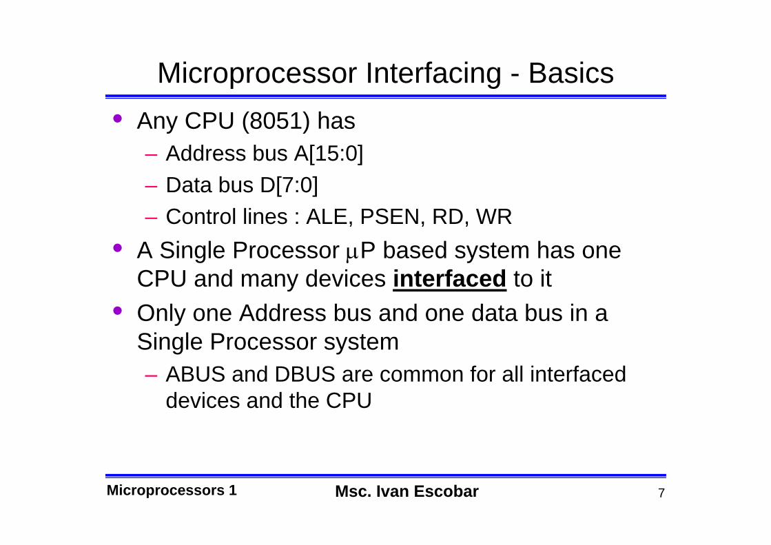
Microprocessor Interfacing - Basics• Any CPU (8051) has
– Address bus A[15:0]– Data bus D[7:0]– Control lines : ALE, PSEN, RD, WR
• A Single Processor µP based system has one CPU and many devices interfaced to it
• Only one Address bus and one data bus in a Single Processor system– ABUS and DBUS are common for all interfaced
devices and the CPU

Msc. Ivan EscobarMicroprocessors 1 8
Microprocessor Interfacing (contd.)• All Microprocessor compatible devices have
enable lines (CE - Chip Enable or CS – Chip Select)– A function of the address bus f(A[15:0]) is
connected to the CE of every device interfaced– This function is unique for every interfaced device
• The CPU accesses each interfaced device by way of this unique function– This function is commonly referred to as the
address of the device

Msc. Ivan EscobarMicroprocessors 1 9
Microprocessor Interfacing (contd.)• Interfaced devices either READ or WRITE or do
BOTH on the DBUS.– Only one device has “exclusive access”– Achieved by using Tri-State buses
• Devices that WRITE to DBUS have CE and RD/OE only– Read Cycle: Assert CE and then assert RD/OE
• Devices that READ and WRITE to DBUS have CE, RD/OE and WR– Write Cycle: Assert CE and then assert WR
Msc. Ivan EscobarMicroprocessors 1 10
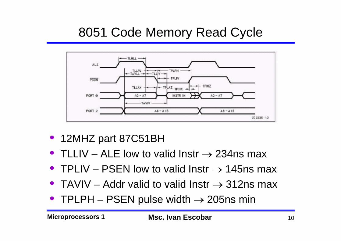
8051 Code Memory Read Cycle
• 12MHZ part 87C51BH• TLLIV – ALE low to valid Instr → 234ns max• TPLIV – PSEN low to valid Instr → 145ns max• TAVIV – Addr valid to valid Instr → 312ns max• TPLPH – PSEN pulse width → 205ns min

Msc. Ivan EscobarMicroprocessors 1 11
8051 Data Memory Read Cycle
• TRLDV – RD Low to valid Data → 252ns max• TAVDV – Addr valid to valid Data → 585ns max• TLLDV – ALE low to valid Data → 517ns max• TRLRH – RD pulse width → 400ns min

Msc. Ivan EscobarMicroprocessors 1 12
8051 – Address Generation• Address Generator
is a piece of hardware that produces unique addresses to each interfaced device
• Example– F1 = A15 . A14– F2 = A15 . A14– F3 = A15 . A14

Msc. Ivan EscobarMicroprocessors 1 13
What is needed ?• Need to know the following for all the devices
before address generator can be designed– Base address of each device
• Where it starts in the address map
– Size of the device• How much of the address space it uses up

Msc. Ivan EscobarMicroprocessors 1 14
Example –1 : 2K Memory at 0x0000• Pins : address – A10 to A0, Data – D7 to D0, RD,
WR, CE• Base address = 0x0000• Size = 2k (2 *1024 = 2048 bytes = 0x0800)• Address Map occupancy
– 0x0000 to 0x07FF that is,– 0000 - 0000 - 0000 - 0000 binary to– 0000 - 0111 - 1111 - 1111 binary
• 11 lowest address bits A10 to A0 have to be connected to the address pins on the memory

Msc. Ivan EscobarMicroprocessors 1 15
Example –1 : (contd.)• Unused address bits are
– A15 to A11• Base address is 0x0000• CE has to be generated if
all the unused address bits are logic-0– CE is active low
• CE = A15 + A14 + A13 + A12 + A11
• Then connect RD and WR1XXXX1
1XXX1X
1XX1XX
1X1XXX
11XXXX
000000
CEA11A12A13A14A15

Msc. Ivan EscobarMicroprocessors 1 16
Example 2: Same Memory at 0x4000• Base address is
0x4000– 0100 0000 0000 0000
• Size is 2K• Unused address bits
– A15 to A11• CE has to be
generated as per the truth-table
• Expression is:
onsoand
1X1X1X
1X0X1X
11XX1X
10XX1X
000010
1XXX0X
CEA11A12A13A14A15
11.12.13.14.15 AAAAACE =

Msc. Ivan EscobarMicroprocessors 1 17
Complete vs. Partial Address Decoding• Complete address decoding:
– Use all unused address bits to generate CE• Partial addressing decoding
– Use a sub-set of the unused address bits– Used to reduce the address generator complexity– Produces address mirrors (same device at multiple
addresses)• Example
– 2K memory at 0x0000, we used A15 to A11– Instead just connect A11 to CE– Same 2K memory device will then be mirrored for all values
of A15 to A12• 0x0000, 0x1000, 0x2000, 0x3000, …. , 0xF000
– Address generator became very simple, but we lost a lot of address space
Msc. Ivan EscobarMicroprocessors 1 18
74138 Decoder for Address Generation• 3 to 8 decoder, available in a single DIP
package.• Takes 3 address lines and generates complete
addressing among those• Example
– Connect A15, A14, A13 to the decoder inputs– Decoder outputs give base addresses for
• 0x0000, 0x2000, 0x4000, 0x6000,0x8000, 0xA000, 0xC000, 0xE000
• For more complicated address decoding:– Play tricks with 74138 enable connections.– Use programmable devices like PALs, PLDs or
FPGAs
Msc. Ivan EscobarMicroprocessors 1 19
External Pure Code Memory• Could be RAM or ROM• Address generation as per standard procedure• Connect PSEN to the OE of the memory device
– RD and WR are ignored• Connect Data bits D7-D0 of the memory and the
8051

Msc. Ivan EscobarMicroprocessors 1 20
External Code + Data Memory• Address generation as per standard procedure• Logically AND PSEN and RD and then connect
to the OE of the memory• Connect WR from the 8051 to WR of the memory• Connect Data bits D7-D0 of the memory and the
8051
Msc. Ivan EscobarMicroprocessors 1 21
External I/O Devices• Same procedure as for interfacing memory• Only difference is that these devices have
smaller sizes and use smaller portions of the address space
• Example:– 8 LEDS connected to an 8-bit latch. The latch is
address mapped to 0xF000. Size is 1byte– 8255 I/O device memory mapped at 0xD000. Size
is 4 bytes
Msc. Ivan EscobarMicroprocessors 1 22
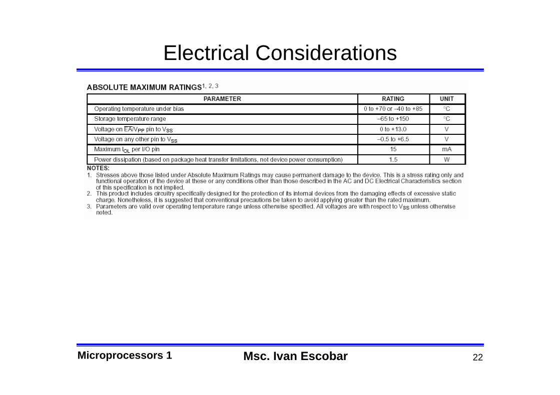
Electrical Considerations

Msc. Ivan EscobarMicroprocessors 1 23
Electrical Characteristics (Contd.)

Msc. Ivan EscobarMicroprocessors 1 24
8051 - Switch On IO Ports• Case-1:
– Gives a logic 0 on switch close
– Current is 0.5ma on switch close
• Case-2:– Gives a logic 1 on
switch close– High current on
switch close• Case-3:
– Can damage port if 0 is output
Msc. Ivan EscobarMicroprocessors 1 25
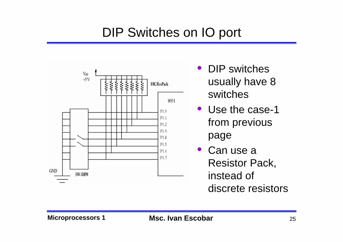
DIP Switches on IO port
• DIP switches usually have 8 switches
• Use the case-1 from previous page
• Can use a Resistor Pack, instead of discrete resistors
Msc. Ivan EscobarMicroprocessors 1 26
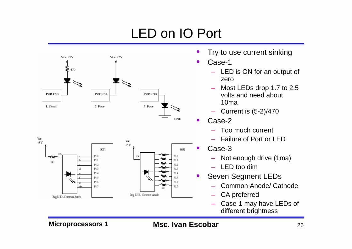
LED on IO Port• Try to use current sinking• Case-1
– LED is ON for an output of zero
– Most LEDs drop 1.7 to 2.5 volts and need about 10ma
– Current is (5-2)/470• Case-2
– Too much current– Failure of Port or LED
• Case-3– Not enough drive (1ma)– LED too dim
• Seven Segment LEDs– Common Anode/ Cathode– CA preferred– Case-1 may have LEDs of
different brightness

Msc. Ivan EscobarMicroprocessors 1 27
8051 Interfacing with the 8255• 8255 - Widely used I/O chip
– 40 pins– Provides 3 eight bit ports PA, PB and PC– Port PC can be used as two 4 bit ports PCL and
PCU– Ports have handshaking ability– Two address lines A0, A1 and a Chip select CS
• Address space of 4 bytes• 00b selects Port A• 01b selects Port B• 10b selects Port C• 11b selects an internal control register
– Read only.

Msc. Ivan EscobarMicroprocessors 1 28
8255 Functional Diagram• CS is used to interface with 8051• If CS is generated from lets say
Address lines A15:A12 as follows,A15:A12 = 1000
• Base address of 8255 is– 1000 xxxx xxxx xx00b– 8000H
• Address of the registers– PA = 8000H– PB = 8001H– PC = 8002H– CR = 8003H

Msc. Ivan EscobarMicroprocessors 1 29
8255 Operating Modes• Mode 0 : Simple I/O
– Any of A, B, CL and CU can be programmed as input or output
• Mode 1: I/O with Handshake– A and B can be used for I/O– C provides the handshake signals
• Mode 2: Bi-directional with handshake– A is bi-directional with C providing handshake signals– B is simple I/O (mode-0) or handshake I/O (mode-1)
• BSR (Bit Set Reset) Mode– C alone is available for bit mode access
• Allows single bit manipulation for control applications.
Msc. Ivan EscobarMicroprocessors 1 30
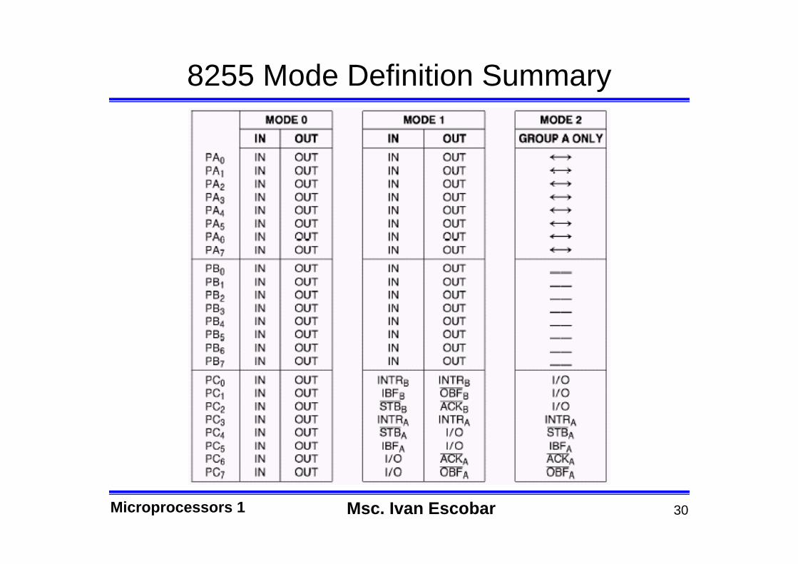
8255 Mode Definition Summary

Msc. Ivan EscobarMicroprocessors 1 31
8255 Configuration• Configured by writing a control-word in CR register• CR definition
– D7 : 1→I/O mode, 0 → BSR– D6,D5 : Mode selection for A and CU
• 00 → Mode0, 01 → Mode1, 1x → Mode2– D4 : Port A control
• 1 → A input, 0 → A output– D3 : Port CU control
• 1 → CU input, 0 → CU output– D2 : Port B Mode selection
• 0 → B is in mode 0, 1 → B is in mode 1– D1 : Port B control
• 1 → B input, 0 → B output– D0 : Port CL control
• 1 → CL input, 0 → CL output• Refer to 8255 datasheet for additional options

Msc. Ivan EscobarMicroprocessors 1 32
8255 Control Word

Msc. Ivan EscobarMicroprocessors 1 33
8255 Usage: Simple Example• 8255 memory mapped to 8051 at address 8000H base
– PA = 8000H, PB = 8001H, PC = 8002H, CR = 8003H• Control word for all ports as outputs in mode0
– CR : 1000 0000b = 80H• Code segment
test: mov A, #80H ; control wordmov DPTR, #8003H ; address of CRmovx @DPTR, A ; write control wordmov A, #55h ; will try to write 55 and AA alternatively
repeat: mov DPTR, #8000H ; address of PAmovx @DPTR, A ; write 55H to PAinc DPTR ; now DPTR points to PBmovx @DPTR, A ; write 55H to PBinc DPTR ; now DPTR points to PCmovx @DPTR, A ; write 55H to PCcpl A ; toggle A (55→AA, AA→55)acall MY_DELAY ; small delay subroutinesjmp repeat ; for (1)

Msc. Ivan EscobarMicroprocessors 1 34
BSR Mode• If used in BSR mode, then the bits of port C can
be set or reset individually.


![Micros Folder 10-2010 - nsc-ksa.comnsc-ksa.com/catalogue/NSC CATALOGUES/Microscopes/Micros/MC300serie.pdfhijgYn XdchigjXi^dc VcY ZVhn ]VcYa^c\ ^i ... micros micros micros micros micros](https://static.fdocuments.in/doc/165x107/5b1c97d97f8b9a2d258ff7ed/micros-folder-10-2010-nsc-ksacomnsc-ksacomcataloguensc-cataloguesmicroscopesmicros.jpg)