Micro-programmable State Machine Design · PDF filePM-based State Machine Implementation Mealy...
54
Micro-programmable State Machine Design Dr. Shoab A Khan
Transcript of Micro-programmable State Machine Design · PDF filePM-based State Machine Implementation Mealy...

Micro-programmable State Machine Design
Dr. Shoab A Khan
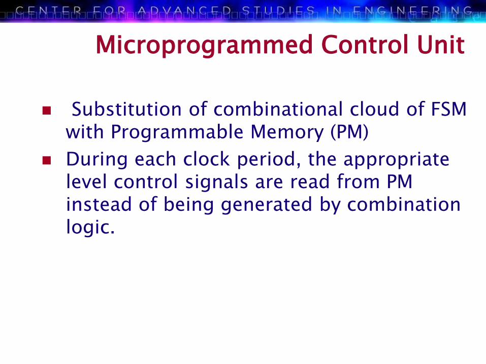
Microprogrammed Control Unit
Substitution of combinational cloud of FSM with Programmable Memory (PM)
During each clock period, the appropriate level control signals are read from PM instead of being generated by combination logic.

PM-based State Machine Implementation
Mealy machine: ROM address bits A0-A5 are function
of Input x1 and x2 and current states S0-S3
A0A1
A2
A3
A4
A5
X1
X2
D Q
D Q
D Q
D Q
S0
S1
S2
S3
D0D1
D3D2
D4
Z1
Z2
Z3Z4
Z5
OUTPUTSINPUTS
D5D6
D8D7
State register
AddressLines
NEXT STATE
clk
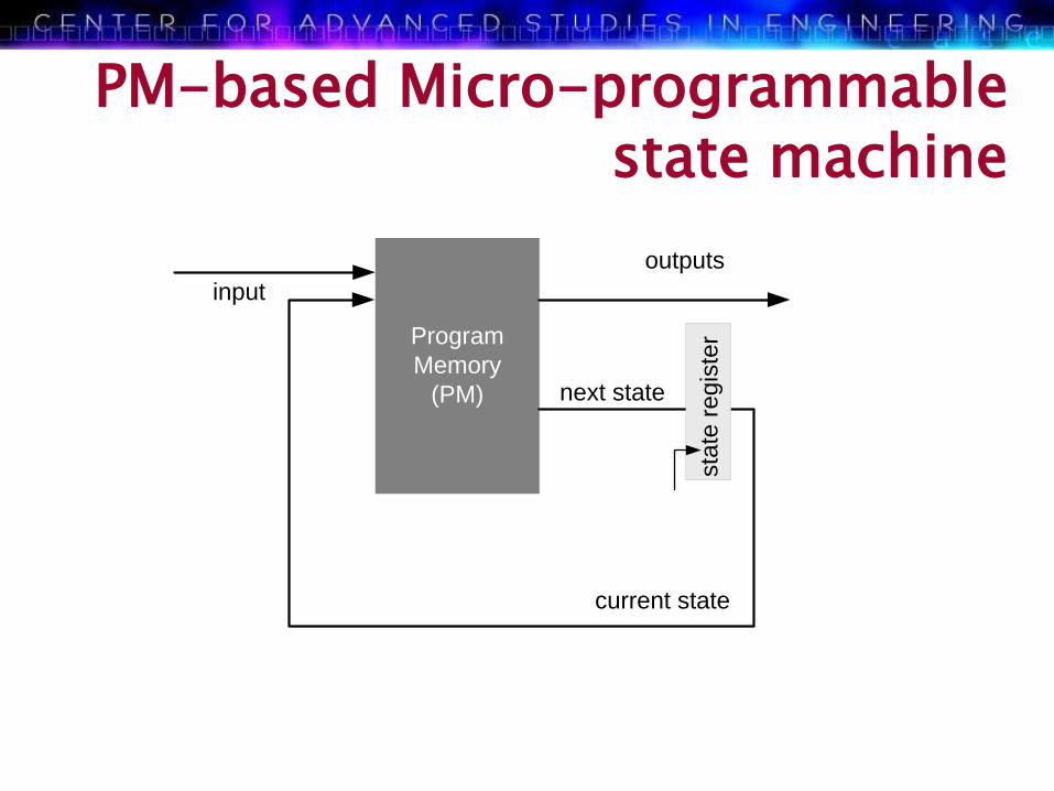
PM-based Micro-programmable state machine
Program
Memory
(PM)
outputs
next state
current state
sta
te r
eg
iste
r
input

Example Design
PM
current state
2
addr
6
9 5
data cntr
4
4 next state
rst_n
input

Micro-programmed Sate Machine Implementation
in
out=0
out=0
in
out=0
out=0
in
out=0
out=0
in
out=0 out=1
2'b00S0
0
1
2'b01S1
0
1
2'b10S2
0
0 1
1
2'b11S3
next_state out
input
current_state
00 0
00 1
01
01
10
10
11
11
1
0
0
1
0
1
addr
0 0 0
0 1 0
0 1
1 0
1 1
0
0
0
0
0
Program Memory
1 0
1 1
0 0 1
input
clk
current_state outrst_n
(a) (b)

Moore Machineout=0
in
out=0
in
out=0
in
out=0
in
3'b000S0
0
1
3'b001S1
0
1
3'b010S2
0
0
1
1
3'b011
out=1
S3
3'b100S4
in1
0
000 0
000 1
001
001
010
010
011
011
100
100
1
0
0
1
0
1
0
1
state register
000
001
001
010
010
011
011
100
001
000
0
0
0
0
1
x
output
14
next state3
addr
input
current state
3
addr PM-I PM-II
3x
x
x
x
do
n’t c
are
(a) (b)
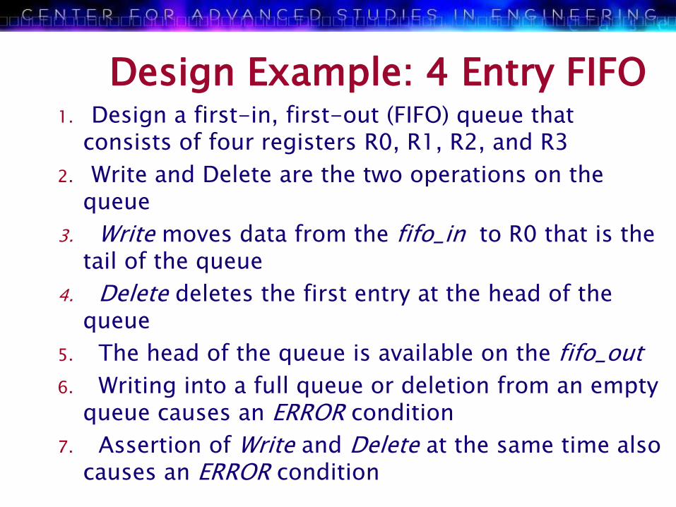
Design Example: 4 Entry FIFO1. Design a first-in, first-out (FIFO) queue that
consists of four registers R0, R1, R2, and R3
2. Write and Delete are the two operations on the queue
3. Write moves data from the fifo_in to R0 that is the tail of the queue
4. Delete deletes the first entry at the head of the queue
5. The head of the queue is available on the fifo_out
6. Writing into a full queue or deletion from an empty queue causes an ERROR condition
7. Assertion of Write and Delete at the same time also causes an ERROR condition
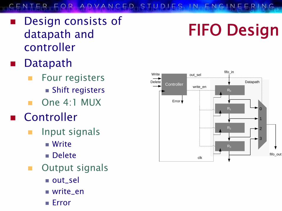
FIFO Design Design consists of
datapath and controller
Datapath
Four registers
Shift registers
One 4:1 MUX
Controller
Input signals
Write
Delete
Output signals
out_sel
write_en
Error
Controller
out_sel
write_en
Write
Delete
fifo_in
fifo_out
R0
R1
R2
R3
Error
0
1
2
3
clk
Datapath

Controller
FSM based design
Mealy machine
Five states
Idle
One entry
Two entries
Three entries
Full
Empty
DelWrite
(fifo_in → R0)
write_en = 1
(R0 → fifo_out)
out_sel = 0
Error
S0 3'b000
0
01
S13'b001
WriteDel
0
0 1Del
11
Error
(R1 → fifo_out)
out_sel = 1
WriteDel
Error
S2 3'b010
0
0 1
0
1
(fifo_in → R0)
(R0 → R1)
write_en = 1
Del
1
(fifo_in → R0)
(R0 → R1)
(R1 → R2)
write_en = 1
(R2 → fifo_out)
out_sel = 2
WriteDel
Error
S3 3'b011
0
0 11
Del
1
(fifo_in → R0)
(R0 → R1)
(R1 → R2)
(R2 → R3)
write_en = 1
0
1
(R3 → fifo_out)
out_sel = 3
WriteDel
Error
S43'b100
0
0 1
0
1
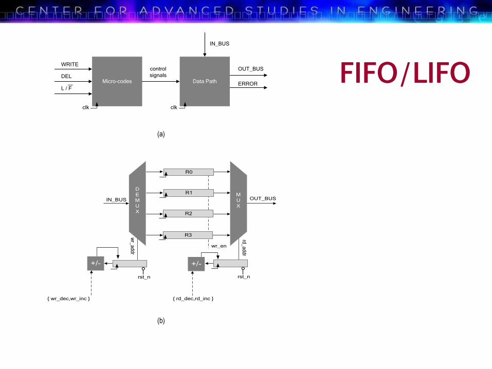
FIFO/LIFOData PathMicro-codes
control
signals
IN_BUS
OUT_BUSWRITE
DEL
L / FERROR
clk clk
(a)
+/- +/-
IN_BUS OUT_BUS
D
E
M
U
X
M
U
X
wr_enrd_addr
wr_addr
{ rd_dec,rd_inc }{ wr_dec,wr_inc }
R0
R1
R2
R3
rst_n rst_n
(b)
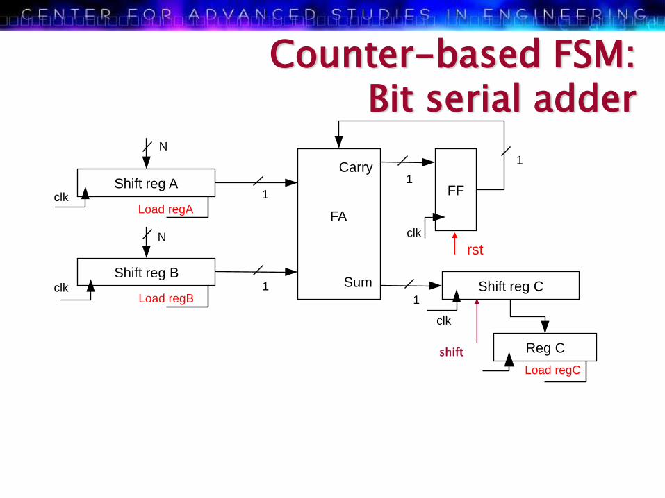
rst
Carry
FA
Sum
Shift reg A
Shift reg B
FF
Shift reg C
Reg C
N
N
Load regA
Load regB
1
1
1
1
1
Load regC
clk
clk
clk
clk
Counter-based FSM:Bit serial adder
shift

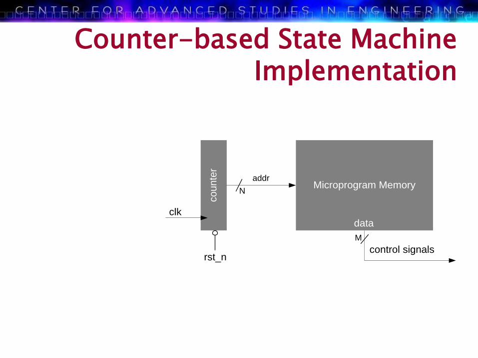
Counter-based State Machine Implementation
Machine useful only in generating sequence of control
Signals without any input
CLR
CO
UN
TE
R
Q0Q1
Qk
A0
A1
Ak
MICROPROGRAM MEMORY(ROM, PROM, EPROM or EEPROM)
CONTROL BITS (DATA Out)
Dm-0
To Architecture
rst_n
clk
Counter-based State Machine Implementation
Microprogram Memory
co
un
ter
rst_n
clkdata
control signals
addr
N
M

Modifications to Counter-based Microcontrollers 1
Mechanism for changing count sequence
Begin another sequence under control of micro-program memory
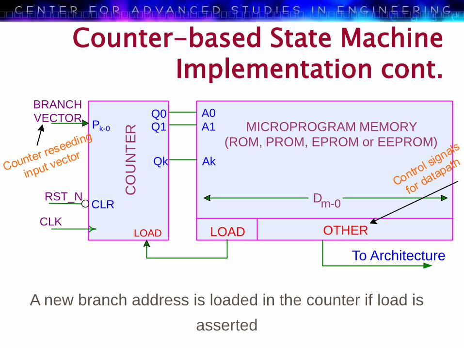
Counter-based State Machine Implementation cont.
A new branch address is loaded in the counter if load is
asserted
PC
OU
NT
ER
Q0Q1
Qk
A0
A1
Ak
MICROPROGRAM MEMORY
(ROM, PROM, EPROM or EEPROM)
To Architecture
BRANCH
VECTOR
CLK
k-0
Dm-0
LOAD OTHER
RST_NCLR
LOAD
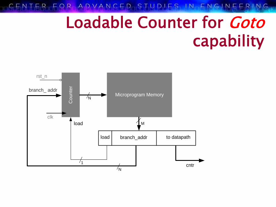
Loadable Counter for Gotocapability
Microprogram Memory
Co
un
ter
rst_n
clk
cntr
load branch_addr to datapath
branch_ addr
N
M
N
1
load

MEMORY
DATAPATH
CONTROL
INP
UT
-OU
TP
UT
A Generic Computing Architecture
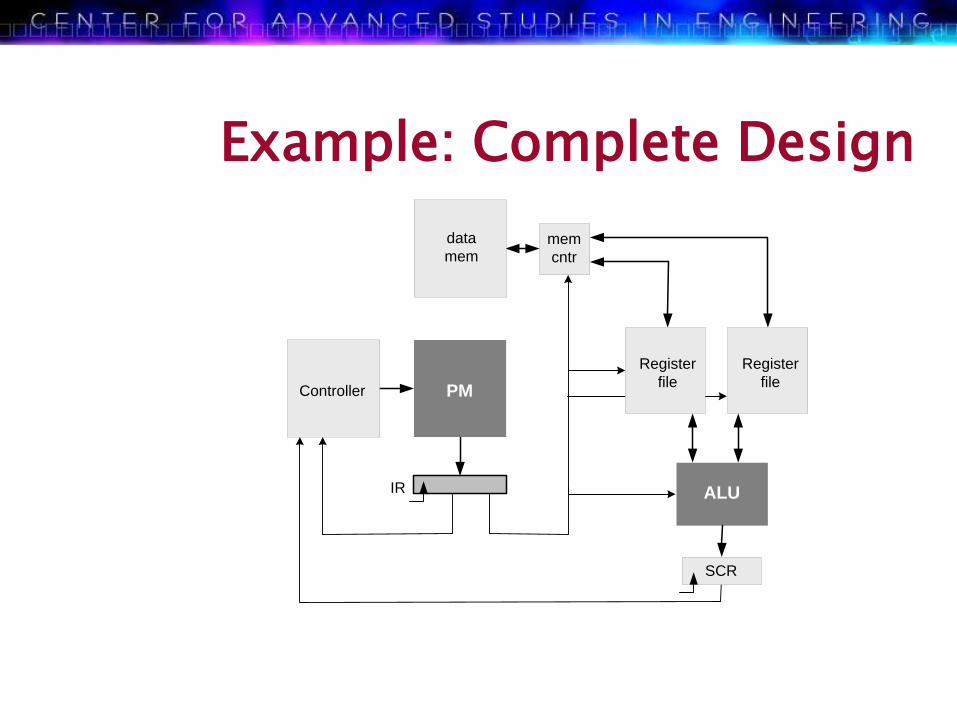
Example: Complete Design
mem
cntr
IR
Register
file
Register
file
ALU
SCR
data
mem
PMController

Modifications to Control-based Microcontrollers 2
Introduction of decision-making capabilities
to microcontroller implementation
Incorporating the branch address in the instruction
The counter loads the branch address if the signal load is asserted

Counter-based ASM with Conditional Branching
When CONDITION =1 counter is reset with branch address
value
LOAD
CO
UN
TE
R
Q0Q1
Qk
A0A1
Ak
MICROPROGRAM MEMORY
To Architecture
SYSCLK
Dm-0
BRANCH ADDRESS LOAD OTHER
RESETCLR
LOAD
Pk-0
2 Words of m+1 bitsK+1
CONDITION
BRANCHVECTOR

Blocking Condition Testing Conditional execution
2-bit control allowing on selection of two conditional inputs and two signals true and false
The conditions come from the status register in the data path
Example: zero and positive flags are used for providing
conditional execution
if (r1 > r2) jump label3; // compute r1-r2 jump if result is positive
if (r1 == r2) jump label1; // compute r1-r2, jump if result is zero
jump label 2 // unconditional jump
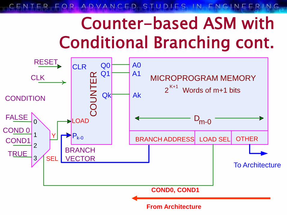
Counter-based ASM with Conditional Branching cont.
CO
UN
TE
R
Q0Q1
Qk
A0
A1
Ak
MICROPROGRAM MEMORY
To Architecture
CLK
Dm-0
BRANCH ADDRESS OTHER
RESETCLR
LOAD
Pk-0
2 Words of m+1 bitsK+1
CONDITION
BRANCH
VECTOR
LOAD SEL
0
1
2
3
FALSE
COND 0
COND1
TRUESEL
Y
From Architecture
COND0, COND1

Conditional Branching Capability
load
0
1
cond_0
cond_1
Microprogram Memory
Co
un
ter
rst_n
clk
cntr
load
selbranch_addr to datapath
branch_addr
N
M
N
2
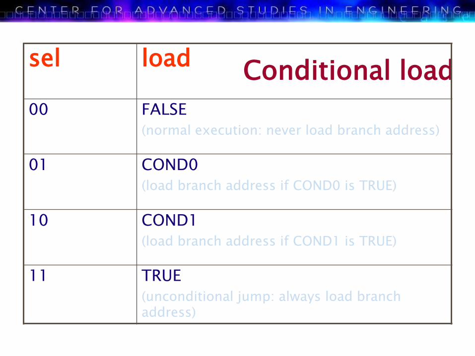
Conditional load sel load
00 FALSE
(normal execution: never load branch address)
01 COND0
(load branch address if COND0 is TRUE)
10 COND1
(load branch address if COND1 is TRUE)
11 TRUE
(unconditional jump: always load branch address)
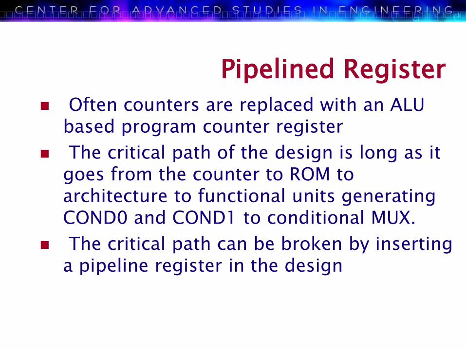
Pipelined Register
Often counters are replaced with an ALU based program counter register
The critical path of the design is long as it goes from the counter to ROM to architecture to functional units generating COND0 and COND1 to conditional MUX.
The critical path can be broken by inserting a pipeline register in the design
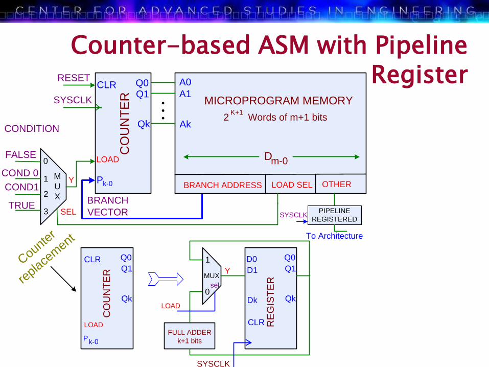
Counter-based ASM with Pipeline Register
CO
UN
TE
R
Q0Q1
Qk
A0
A1
Ak
MICROPROGRAM MEMORYSYSCLK
Dm-0
BRANCH ADDRESS OTHER
RESETCLR
LOAD
Pk-0
2 Words of m+1 bitsK+1
CONDITION
BRANCH
VECTOR
LOAD SEL
0
1
2
3
FALSE
COND 0
COND1
TRUESEL
Y
CO
UN
TE
R
Q0
Q1
Qk
CLR
LOAD
Pk-0
M
U
X
0
1
MUXR
EG
IST
ER
Q0
Q1
Qk
CLR
D0
D1
DkLOAD
sel
FULL ADDER
k+1 bits
Y
SYSCLK
Counter
repla
cem
ent
PIPELINE
REGISTERED
To Architecture
SYSCLK

Micro PC Based Controller
+
1
Microprogram Memory
cond
sel
branch
addrcntr
signals
0
1
cond 0cond 1
to datapath
from datapath
ne
xt a
dd
r mux
mic
ro P
Ccon
d m
ux
addr bus
data bus
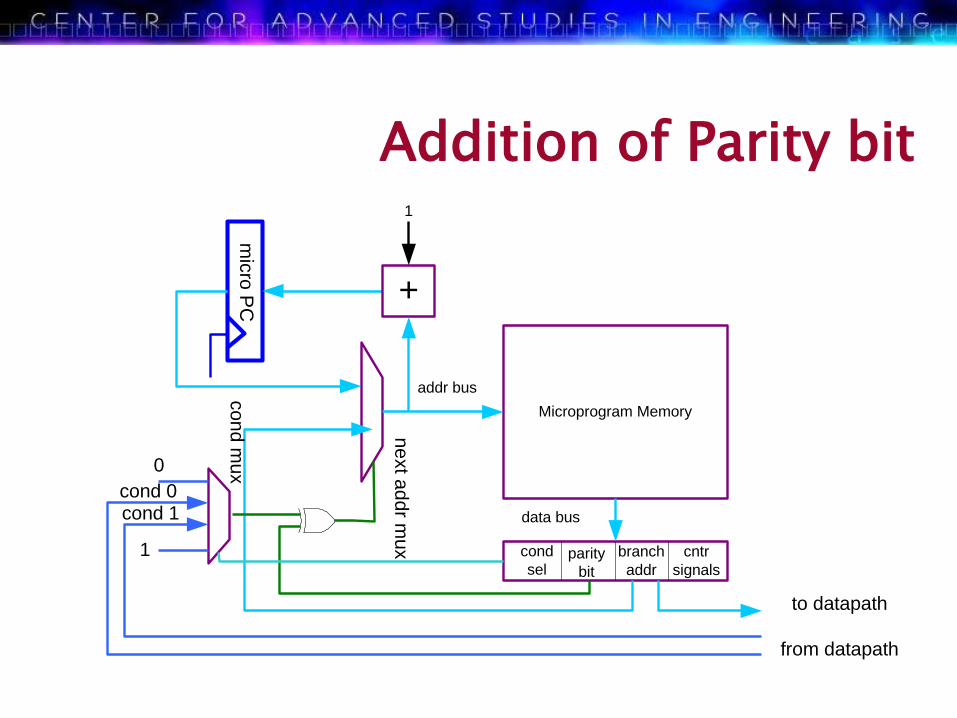
Addition of Parity bit
+
1
Microprogram Memory
cond
sel
branch
addr
cntr
signals
0
1
cond 0cond 1
to datapath
from datapath
ne
xt a
dd
r mux
mic
ro P
Ccon
d m
ux
addr bus
data bus
parity
bit

Controller with data path
+
1
Microprogram Memory
cond
sel
branch
addr
cntr
signals
0
1
cond 0cond 1
to datapath
from datapath
ne
xt a
dd
r mux
mic
ro P
Cco
nd
mu
x
addr bus
data bus
parity
bit
ALU
Z N
ALU status
R0
R1
register file

Instruction word design
cond sel parity label out sel src 1 src 2 dst
2 1 2 3 3 3
22
8
(a)
type
sellabel
src 1 src 2 dst
1 2 8
12
cond sel
out sel
parity
2 3 3 3
1
(b)

Conditional Braching Conditional execution
2-bit control allowing on selection of two conditional inputs and two signals true and false.
A parity bit for inverse selection of the condition
Example: zero and positive flags are used for providing conditional
execution
Inverse selection is provided by parity bit
if (r1 > r2) jump label3; // compute r1-r2 jump if result is positive
if (r1 < r2) jump label3; // compute r1-r2 jump if result is negative (positive flag 0 and polarity bit is set)
if (r1 = r2) jump label1; // compute r1-r2, jump if result is zero
if (r1 != r2) jump label1; // compute r1-r2, jump if result is not zero (zero flag is 0 and polarity bit is set)
jump label 2 // unconditional jump

micro PC-based ASM with Condition Multiplexer
+
1
Microprogram Memory
cond
sel
branch
addr
cntr
signals
0
1
cond 0cond 1
to datapath
from datapath
ne
xt a
dd
r mux
mic
ro P
C
addr bus
data bus
parity
bit
branch addr 0
branch addr 1
next
addr
selnext
addr sel

Subroutine Execution
Temporary storage location added for the copy of contents of mPC register
Register referred to as Subroutine Return Address Register
Address kept in register allows on returning to next address of microprogram execution after complete subroutine call

Register-based Controller with Subroutine Capability
+
1
Microprogram Memory
cond
sel
branch
addr
cntr
signals
0
1
cond 0cond 1
to datapath
from datapath
ne
xt a
dd
r mux
mic
ro P
C
addr bus
data bus
parity
bit
branch addr 0branch addr 1
next
addr
selnext
addr sel
su
b re
trun a
ddr re
g

Design Problem Opcode Instruction Description
0000
0011
0010
0001
1101
1100
1011
1010
1001
1000
0111
0110
0101
0100
cRACC i
ji RRACC
kji RRRACC
cRRRACC kji
ji RRACC *
LoadiR
iRStore
Load n
Branch if Acc = 0
Branch if Acc < 0
Always Branch
Call Subroutine
Return
Acc = <<>> niR
Signed addition of two registers
Signed addition of three registers
Addition of three registers and a constant
Multiplication of 8 LSBs of two registers
Load register into accumulator
Store the contents of the accumulator to register
Load an integer into accumulator
Branch if accumulator is zero
Branch if accumulator is negative
Unconditional branch
Jump to subroutine address
Return from a subroutine call
Right or left shift a register by 16, result inAccumulator
Add a constant into iR

MEMORY
Decode
Combination cloud
xxxx xxx xx xx xx
OpcodeSign
bits Ri R j Rk
PC
++
Su
bre
g
Subreg
PC
Jump
4 to 2
Comp
0
1
2
3
Mul
8 Bit
Logic
Shifter
R0
R1
R2
R3
R i
R j
Rk
CPA
ACC
0
0
0
Store Ri
8 8
Shift
Load Ri
LDI

Arithmetic Insts
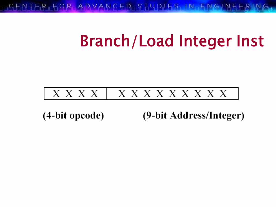
Branch/Load Integer Inst

Storing ACC in a register

Nested Subroutine Nested Subroutine Execution
Subroutine Return Address Register replaced by Subroutine Return Address Memory of stack structure
Possibility to store more than one return address – necessity in implementing nested subroutine calls
Up/down counter (TOP OF STACK) added for stack pointer manipulations

Micro-PC Controller with Nested Subroutine Capability
+
1
Microprogram Memory
cond
sel
branch
addr
cntr
signals
0
1
cond 0cond 1
to datapath
from datapath
ne
xt a
dd
r mu
x
mic
ro P
C
addr bus
data bus
parity
bit
branch addr 0branch addr 1
next
addr
selnext
addr sel
Su
b ro
utin
e
retu
rn
ad
dr s
tack
Top of stack pointer
updown

Nested Subroutine Support
Stack Pointer logic
call
sub
Return Address
Stack
from PC
return
incremented
rst_n
clk
current2
write_en
N
1
write_lifo_addr
read_lifo_addr
to next_address_mux
push
4 levels of nesting
1 stack
Stack Pointer Reg.
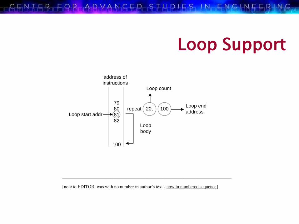
Loop Support
79
80
81
82
100
address of
instructions
Loop start addrrepeat
Loop
body
10020,
Loop count
Loop end
address
__________________________________________________________________________
[note to EDITOR: was with no number in author’s text - now in numbered sequence]
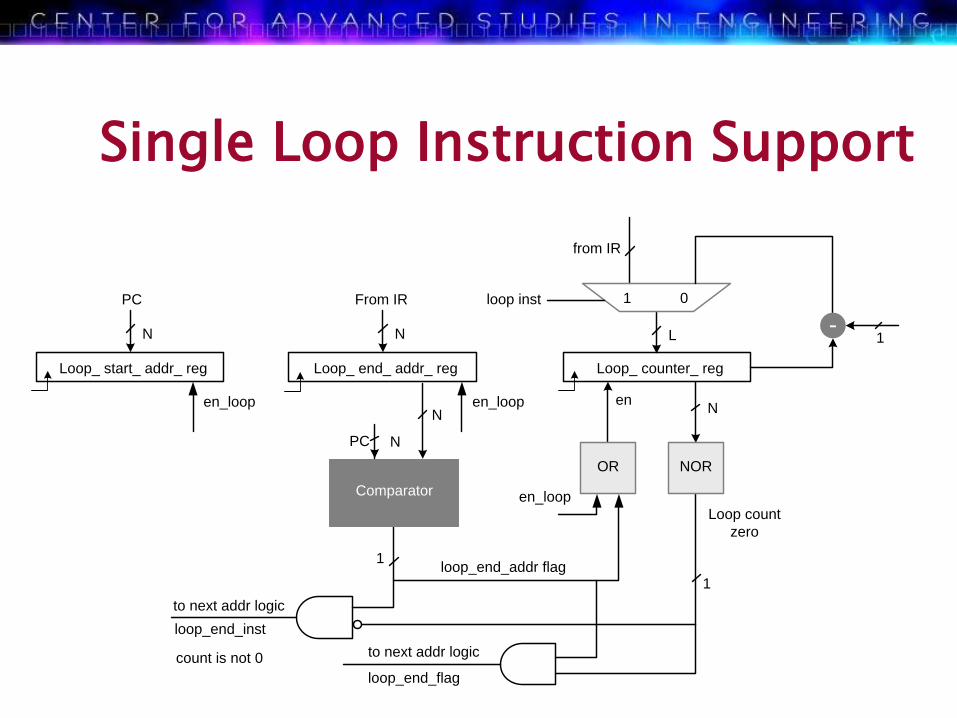
Single Loop Instruction Support
Comparator
Loop_ start_ addr_ reg Loop_ end_ addr_ reg Loop_ counter_ reg
PC
N
From IR
N L
1 0
from IR
loop inst
en_loopN
NPC
OR NOR
Nen
Loop count
zero
loop_end_addr flag1
-1
en_loop
en_loop
1
loop_end_inst
to next addr logic
loop_end_flag
to next addr logiccount is not 0

Nested Loop Support
2324 repeat (5) 352526 repeat (10) 35272829 repeat (20) 343031 repeat (12) 3332333435
25
27
30
32
Loop start
addr
35
35
34
33
Loop end
addr
5
10
20
12
Loop count
(a) (b)

Loop Machine
rst_n
write_en
incremented
Start Address
Stack
From
PC
To Next Address
Generation Unit
N
End Address
Stack
from
Microcode
current
2
N
N
Loop Count
Stack
current2
Push SP OR
Loop End Flag
L
end_addr fields
comparator
PCN
Down Counter clk
L
L
NORZero
Check
Logic
Loop_Count
fields from micro-
code
loop instr
current2
2
2
Stack Pointer logic
rst_n
clk1
1
1
To Next Address
Generation Unit
1
pu
sh
dec
N
loop-end-flag loop-end-instr-flag
0
1
2
3
loop count not 0


4x4bit
register file
64-deep
program ROM
IR
Combinational
logic
Register file read ports
Arithmatic unit Logical unitMultiplication
unti
Selection between
datapath unit outputs
controls
4-bit wide 64-
deep Data
ROM
address
input datar_
ou
t
output data
output data valid
Combinational
logic
PC
address
controls
Loop
machine
Subroutine
stackcontrols
Ovf, Z, P flags
IR


ref_frames( i+k, j+l)
data
movement
target_frame
...
. . .
......
..
.
..
.
.
Loop
machine
tx
ty
controller
SAD
extended register cloumnref_blk_reg_file
extended register row
r (k,l)
acc
_
min_SAD x y
min_flag
rst_n
Example: Motion Estimation

next columncurrent block
next row
Last target block in first row
daisy
chain
search
target