Methodology for Electromigration Signoff in the … degradation and timing failures. Even as modern...
7
Methodology for Electromigration Signoff in the Presence of Adaptive Voltage Scaling Wei-Ting Jonas Chan t , Andrew B. Kahng H and Siddhartha Nath + T ECE and + CSE Departments, UC San Diego, La Jolla, CA 92093 { wechan, abk, sinath } @ucsd.edu Abstct-Electromigration (EM) is a growing reliability concern in sub-22nm technology. Design teams must apply guardbands to meet EM lifetime requirements, at the cost of performance and power. However, EM lifetime analysis cannot ignore front-end reliability mechanisms such as bias temperature instability (BTl). Although the gate delay degradation due to BTl can be compensated by adaptive voltage scaling (AVS), any elevated supply voltage will accelerate EM degradation and reduce lifetime. Since the degradation of BTl is front-loaded, AVS can increase electrical stress on metal wires relatively early during Ie lifetime, which can significantly decrease electromigration reliability. In this paper, we study the "chicken-egg" interlock among BTl, AVS and EM and quantify timing and power costs of meeting EM lifetime requirements with full consideration of BTl and AVS mechanisms. By applying existing statistical and physical EM models, we demonstrate that without such considerations, the inaccuracy (reduction) of EM lifetime due to improper guardband against BTl at signoff can be as high as 30% in a 28nm FDSOI foundry technology. Furthermore, we provide signoff guidelines which suggest that the lifetime penalty can be compensated by paying a penalty of up to 1.6% in area and 6% in power. We also demonstrate that suboptimal choice of voltage step size and scheduling strategy can result in up to 1.5 years of decreased EM lifetime. I. INTRODUCTION Reliability signoff is critical in modern sub-22nm technology nodes to guarantee that an IC product operates at a minimum acceptable performance through out its lifetime [14]. Recently, the most important reliability mechanisms for IC design teams are bias temperature instability (BTl) and electromigration (EM) [14] [30] [31]. BTl degrades chip performance by slowing down device switching speeds in critical paths. EM can increase wire resistance, which can cause voltage drop resulting in device slowdown; it can also cause permanent failures in circuits due to shorts or opens. To meet performance requirements, design teams overcome performance degradation due to BTl by applying adaptive Permission to make digital or hard copies of all or part of this work for personal or classroom use is granted without fee provided that copies are not made or distributed for profit or commercial advantage and that copies bear this notice and the full citation on the first page. Copyrights for components of this work owned by others than ACM must be honored. Abstracting with credit is permitted. To copy otherwise, or republish, to post on servers or to redistribute to lists, requires prior specific permission and/or a fee. Request permissions om [email protected]. SLIP 14, June 01 - 02 2014, San Francisco, CA, USA Copyright 2014 ACM 978-1-4503-3053- 4114/06 $15.00. http://dx.doi.orgllO.1145/2633948.2633950 voltage scaling (AVS) [8]. To meet lifetime requirements, design teams overcome mean time to failure (MTTF) with respect to EM-induced interconnect voids and shorts by applying design guardbands [19] [l3] [24] [21]. Sometimes, design teams can try to make interconnects 'immortal' by limiting segment lengths to be less than or equal to the Blech length [7]. However, recent analysis shows that immortality is not guaranteed under all operating conditions [21]. The authors of [21] demonstrate that under long-time electrical stress, all power and ground interconnects suffer om EM degradation which results in larger wire resistances and can cause supply voltage drop (IR drop). IR drop can result in delay degradation and timing failures. Even as modern designs use AVS to compensate the delay degradation, the higher supply voltages can accelerate EM failures [14]. Hence, design teams are forced to use larger margins to guardband against delay degradation, that is, sign off at either a lesser lifetime or lesser performance. This dilemma induces a "chicken-and-egg" loop in the signoff flow as shown in Figure 1. To our best understanding, the interaction between BTl-induced AVS and EM in the context of this chicken-and-egg loop has not been studied in previous works. This motivates us to study EM-aware signoff for systems that use AVS. ) Derated Llbranes Fig. 1. Illustration of the chicken-and-egg loop for circuit signoff with EM and AVS to compensate for performance degradation due to BTl. In this work, we study the effects of EM on both signal and power/ground interconnects using recent models [21]. We quantify impact on circuit performance, power and lifetime in a system that uses AVS. We empirically demonstrate that EM-awareness can change power and area tradeoffs when designers choose corners for AVS signoff. Furthermore,
Transcript of Methodology for Electromigration Signoff in the … degradation and timing failures. Even as modern...

Methodology for Electromigration Signoff in the Presence of Adaptive Voltage Scaling
Wei-Ting Jonas Chant, Andrew B. KahngH and Siddhartha Nath+
TECE and +CSE Departments, UC San Diego, La Jolla, CA 92093 {wechan, abk, sinath} @ucsd.edu
Abstract-Electromigration (EM) is a growing reliability concern in sub-22nm technology. Design teams must apply guard bands to meet EM lifetime requirements, at the cost of performance and power. However, EM lifetime analysis cannot ignore front-end reliability mechanisms such as bias temperature instability (BTl). Although the gate delay degradation due to BTl can be compensated by adaptive voltage scaling (AVS), any elevated supply voltage will accelerate EM degradation and reduce lifetime. Since the degradation of BTl is front-loaded, AVS can increase electrical stress on metal wires relatively early during Ie lifetime, which can significantly decrease electromigration reliability. In this paper, we study the "chicken-egg" interlock among BTl, AVS and EM and quantify timing and power costs of meeting EM lifetime requirements with full consideration of BTl and AVS mechanisms. By applying existing statistical and physical EM models, we demonstrate that without such considerations, the inaccuracy (reduction) of EM lifetime due to improper guard band against BTl at signoff can be as high as 30% in a 28nm FDSOI foundry technology. Furthermore, we provide signoff guidelines which suggest that the lifetime penalty can be compensated by paying a penalty of up to 1.6% in area and 6% in power. We also demonstrate that suboptimal choice of voltage step size and scheduling strategy can result in up to 1.5 years of decreased EM lifetime.
I. INTRODUCTION
Reliability signoff is critical in modern sub-22nm technology nodes to guarantee that an IC product operates at a minimum acceptable performance through out its lifetime [14]. Recently, the most important reliability mechanisms for IC design teams are bias temperature instability (BTl) and electromigration (EM) [14] [30] [31]. BTl degrades chip performance by slowing down device switching speeds in critical paths. EM can increase wire resistance, which can cause voltage drop resulting in device slowdown; it can also cause permanent failures in circuits due to shorts or opens. To meet performance requirements, design teams overcome performance degradation due to BTl by applying adaptive
Permission to make digital or hard copies of all or part of this work for personal or classroom use is granted without fee provided that copies are not made or distributed for profit or commercial advantage and that copies bear this notice and the full citation on the first page. Copyrights for components of this work owned by others than ACM must be honored. Abstracting with credit is permitted. To copy otherwise, or republish, to post on servers or to redistribute to lists, requires prior specific permission and/or a fee. Request permissions from [email protected]. SLIP 14, June 01 -02 2014, San Francisco, CA, USA Copyright 2014 ACM 978-1-4503-3053-4114/06 $15.00. http://dx.doi.orgllO.1145/2633948.2633950
voltage scaling (AVS) [8]. To meet lifetime requirements, design teams overcome mean time to failure (MTTF) with respect to EM-induced interconnect voids and shorts by applying design guardbands [19] [l3] [24] [21]. Sometimes, design teams can try to make interconnects 'immortal' by limiting segment lengths to be less than or equal to the Blech length [7]. However, recent analysis shows that immortality is not guaranteed under all operating conditions [21]. The authors of [21] demonstrate that under long-time electrical stress, all power and ground interconnects suffer from EM degradation which results in larger wire resistances and can cause supply voltage drop (IR drop). IR drop can result in delay degradation and timing failures.
Even as modern designs use AVS to compensate the delay degradation, the higher supply voltages can accelerate EM failures [14]. Hence, design teams are forced to use larger margins to guardband against delay degradation, that is, sign off at either a lesser lifetime or lesser performance. This dilemma induces a "chicken-and-egg" loop in the signoff flow as shown in Figure 1. To our best understanding, the interaction between BTl-induced AVS and EM in the context of this chicken-and-egg loop has not been studied in previous works. This motivates us to study EM-aware signoff for systems that use AVS.
) Derated Llbranes
Fig. 1. Illustration of the chicken-and-egg loop for circuit signoff with EM and AVS to compensate for performance degradation due to BTl.
In this work, we study the effects of EM on both signal and power/ground interconnects using recent models [21]. We quantify impact on circuit performance, power and lifetime in a system that uses AVS. We empirically demonstrate that EM-awareness can change power and area tradeoffs when designers choose corners for AVS signoff. Furthermore,
we demonstrate that different AVS strategies have different impacts on EM lifetimes. We conduct our experiments with a 28nm FDSOI foundry technology and commercial tool flows.
Our contributions are sununarized as follows.
(1) We analyze interactions between EM degradation, and AVS signoff and scheduling, in a 28nm foundry FDSOI technology using commercial EDA tool flows. We address the three-way interactions between EM, BTl and AVS, and demonstrate that these interactions are significant at 28nm and beyond.
(2) We study the incremental cost of design to prevent EM relative to ignoring EM at signoff. We perform our analyses, with both modeling as well as ignoring of AVS signoff and scheduling.
(3) We demonstrate that the inaccuracy (penalty) of EM lifetime due to improper guardband against BTl at signoff can be as high as 30% in a 28nm technology. Furthermore, we demonstrate that choice of AVS voltage step size and scheduling strategies can result in up to 1.5 years of decreased EM lifetime.
(4) We provide signoff guidelines which suggest that the EM lifetime penalty can be compensated by paying an area penalty of up to 1.6% and a power penalty of up to 6%.
The remainder of the paper is organized as follows. In Section II, we review related works on AVS and EM signoff. In Section III, we study implications of a recent statistical EM model in AVS systems, and in Section IV, we describe our design of experiments and present results. In Section V, we describe future works and conclude the paper.
II. REL ATED WORKS ON AVS SIGNOFF
Several previous works address different aspects of EM. We taxonomize these works into three categories. (a) Models for lifetime and wire degradation due to
EM. Black proposes an empirical mean time to failure (MTTF) model of wires [6], which is the well-known Black's Equation. Arnaud et al. [4] and Federspiel et al. [11] study the failure processes in copper wires and extend Black's Equation. While previous works focused on developing physical models, Mishra et al. [21] propose a statistical model of the process of EM degradation. They demonstrate that their modeling approach can reduce the pessimism in Black's Equation-based EM signoff criteria. (b) Approaches for EM evaluation and signoff. EM evaluations and optimizations in EDA tools rely on CPUintensive computations and layout optimizations to constrain current densities that satisfy EM lifetime requirements. [28] [38] [36]. As technology advances, more physical design factors such as temperature [10], process variation [24], and growing dominance of BTl and AVS must be considered in order to achieve accurate EM evaluation and signoff. (c) Physical design approaches for EM-durable circuits. In this category, we include wire-sizing and wire segmentation methods for the design of EM-durable circuits. Adler et al. [1] [2], Jiang et al. [12], Lienig et al. [19] and Yan et al. [26] develop wire-sizing algorithms for current-aware
routers that avoid high current densities in circuits. They guarantee lifetime by ensuring that their algorithms always deliver current densities that are within the limits specified in technology files. Li et al. [18] develop wire segmentation and via insertion algorithms to create immortal wires by constraining interconnect segment lengths to be less than the Blech length [18].
Previous works on BTl in AVS systems [5] [9] [15] [16] [17] [20] [23] focus on the interactions between behaviors of AVS and BTl while ignoring EM degradation. Recently, Chan et al. [8] study sign off strategies that consider interactions between AVS and BTl, but do not consider EM in their work.
Our work falls at the intersection of categories (b) and (c), building on that of [8]. We consider EM signoff strategies in the presence of BTl and AVS, and we investigate approaches to the design of EM-durable circuits. To the best of our knowledge, we are the first to address the three-way interactions between EM, BTl and AVS, and to demonstrate that these interactions are significant at 28nm and beyond.
III. IMPLIC ATIONS OF A RECENT STATISTIC AL EM MODEL
We now study the implications of a recent statistical EM model [21] on system performance. The model is a function of wire geometry, electric field due to the supply voltage VDD, and ambient temperature, and estimates degradation due to increased resistance on wires. We first verify correctness of the model in a 28nm foundry FDSOI technology and then quantify the delay impact due to EM on AVS systems. In our evaluations in Section IV, we use both the statistical as well as the traditional lifetime model using Black's Equation [6].
A. Characterization of EM Model In previous works, such as [4] and [11], circuit
measurements and empirical models demonstrate that the failure of wires due to EM has two stages. In the first stage (nucleation), height of void is less than the thickness of copper layer, so the wire resistance does not change significantly. Once the void occupies the whole cross-section of the wire, the degradation enters the second stage (growth) and the resistance of the wire suddenly jumps since the liner layer (tantalum), which has relatively higher resistance than copper, below the copper layer becomes the only conducting path in the void region. The jump in resistance occurs when the void height reaches the thickness of the copper layer. After this, the resistance increases linearly and finally causes defects in the wire. We model the time to reach the growth stage and the corresponding void lengths as random variables. We then apply the model in [21] to evaluate the impact of EM on circuit performance.
We use similar EM parameters as in [21] and apply the model to a 28nm technology BEOL process with W =
100nm (2X minimum width to avoid pessimism) and L =
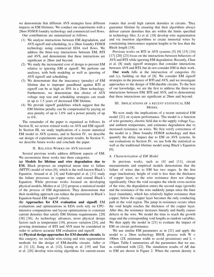
150,um. Table I summarizes all the parameters that we use, as confirmed with [22]. The simulation results of M due to EM are shown in Figure 2. When the current density is
l 0 a:
a: <1
120 ,,==���===o,",----�------, -+- J = 0.1 MAlcm2 : 1 -f)- J = 0.05MAlcm2
100 ...... J = 0.01 MAlcm2
80
60
40
20
- , 10 15 Observation Time (year)
Fig. 2. Interconnect resistance increase in percentage due to different current densities in 28nm BEOL technology.
TABLE I EM AND BEOL PARAMETERS.
Definition Value Units PCu Resistivity of copper 2.50xI0-' D.lm PTa Resistivity of Tantalum liner 3.IOx10 D.lm
T Temperature 125 °C
Gc Effective critical stress for void nucleation 4.lOx 10 Pa G,h T hreshold for thermal stress 0 Pa
Z;rr Effective charge number 5 Do Diffusivity constant in Arrhenius' relation 9.80x 10-" mL Isec kB Boltzmann constant 1.38x 10 -L.' .11K
e Charge of single electron 1.60 x 10 C nell Atomic volume of copper 1.18x10-LY Ill'
B Effective bulk modulus lOY Pa ilEa Mean of activation energy 7.52xI0-LU .I GEa Standard deviation of activation energy 8.00x 10-LL .I
W Copper wire width 100 nm L Copper wire length 150 pm
�vire T hickness of (Cu + Ta) 100 nm TTa T hickness of Ta 5 nm
low (O.OlMA/ cm2), then the wire is inunortal because the process of nucleation is too slow to form voids in copper wires. When the current density is high (0.lMA/cm2), the process of nucleation is fast, and the resistivity increases rapidly and results in significant delay degradation. When the current density is in between the low and high values (0.05MA/cm2), nucleation starts later than, but degrades at a similar rate as, when the current density is O.lMA / cm2.
B. Impact of EM-Induced Performance Degradat ion in AVS
Systems
We now assess the impact of EM degradation on wires for logic and clock signals and for power and ground distribution.
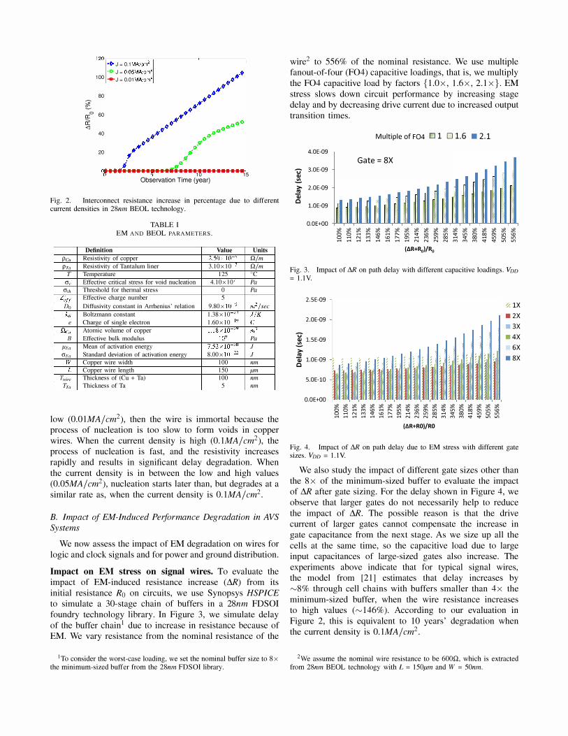
Impact on EM stress on signal wires. To evaluate the impact of EM-induced resistance increase (M) from its initial resistance Ro on circuits, we use Synopsys HSPICE
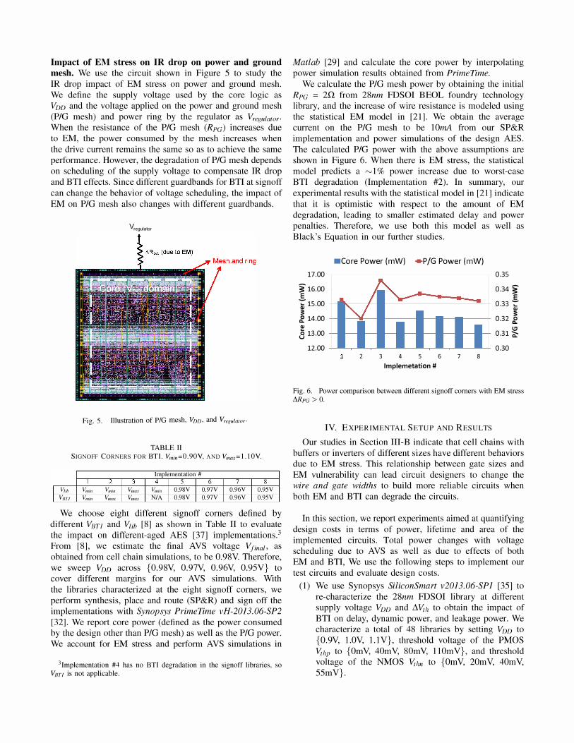
to simulate a 30-stage chain of buffers in a 28nm FDSOI foundry technology library. In Figure 3, we simulate delay of the buffer chain! due to increase in resistance because of EM. We vary resistance from the nominal resistance of the
ITo consider the worst-case loading, we set the nominal buffer size to 8x the minimum-sized buffer from the 28nm FDSOI library.
wire2 to 556% of the nominal resistance. We use multiple fanout-of-four (F04) capacitive loadings, that is, we multiply the F04 capacitive load by factors {l.0 x , l.6 x , 2.1 x } . EM stress slows down circuit performance by increasing stage delay and by decreasing drive current due to increased output transition times.
4.0E-09
i 3.0E-09
� � 2.0E-09 Qj C
1.0E-09
O.OE+OO *- *-0 0 0 .-< .-< .-<
Multiple of F04 D 1 D 1.6 .2.1
Gate = 8X
*- *- *- *- *- *- *- *- *- *- *- *- *- *- *- *- *-.-< '" <D .-< r-- '" ..,. <D '" '" ..,. '" 0 00 '" '" <D N '" ..,. <D r-- '" .-< '" '" 00 .-< ..,. 00 .-< '" 0 '" .-< .-< .-< .-< .-< .-< N N N N '" '" '" ..,. ..,. '" '" {IIR+Rol/Ro
Fig. 3. Impact of M on path delay with different capacitive loadings. Voo = 1.1 V.
2.SE-09
2.0E-09
'U � 1.SE-09
> <tI Qj 1.0E-09 C
S.OE-lO
O.OE+OO *- *-0 0 0 .-< .-< .-<
*- *- *- *- *- *-.-< '" <D .-< r-- '" N '" ..,. <D r-- '" .-< .-< .-< .-< .-< .-< *- *- *- *- *-..,. <D '" '" ..,. .-< '" '" 00 .-< N N N N '"
{IIR+ROl/RO
*- *- *- *-'" 0 00 '" ..,. 00 .-< '" '" '" ..,. ..,. *-'" 0 '"
*-<D '" '"
� IX .2X � 3X .4X m6X .8X
Fig. 4. Impact of M on path delay due to EM stress with different gate sizes. Voo = 1.1 Y.
We also study the impact of different gate sizes other than the 8 x of the minimum-sized buffer to evaluate the impact of M after gate sizing. For the delay shown in Figure 4, we observe that larger gates do not necessarily help to reduce the impact of M. The possible reason is that the drive current of larger gates cannot compensate the increase in gate capacitance from the next stage. As we size up all the cells at the same time, so the capacitive load due to large input capacitances of large-sized gates also increase. The experiments above indicate that for typical signal wires, the model from [21] estimates that delay increases by rv8% through cell chains with buffers smaller than 4x the minimum-sized buffer, when the wire resistance increases to high values (rv 146%). According to our evaluation in Figure 2, this is equivalent to lO years' degradation when the current density is O.lMA / cm2.
2We assume the nominal wire resistance to be 600Q, which is extracted from 28nm BEOL technology with L = 150,um and W = 50nm.
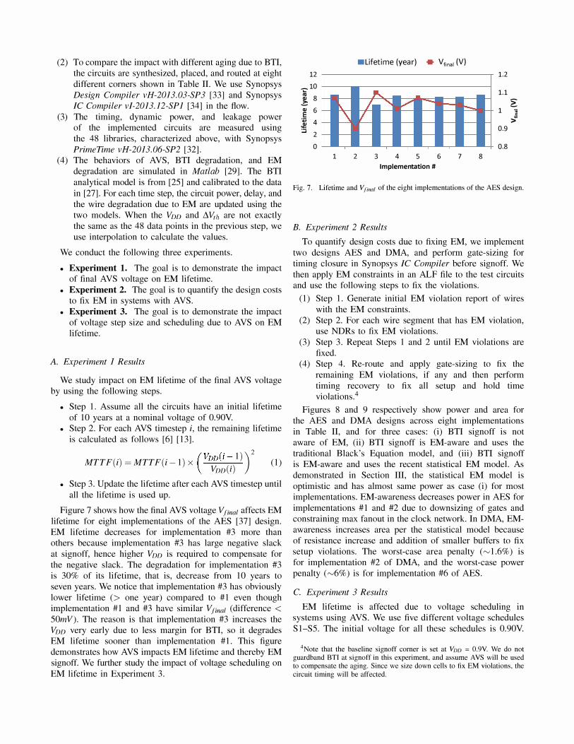
Impact of EM stress on IR drop on power and ground
mesh. We use the circuit shown in Figure 5 to study the IR drop impact of EM stress on power and ground mesh. We define the supply voltage used by the core logic as Voo and the voltage applied on the power and ground mesh (PIG mesh) and power ring by the regulator as Vregulalor. When the resistance of the PIG mesh (Rpc) increases due to EM, the power consumed by the mesh increases when the drive current remains the same so as to achieve the same performance. However, the degradation of PIG mesh depends on scheduling of the supply voltage to compensate IR drop and BTl effects. Since different guardbands for BTl at signoff can change the behavior of voltage scheduling, the impact of EM on PIG mesh also changes with different guardbands.
I Vlih I VB'n
Vregulator
Fig. 5. Illustration of PIG mesh, VDD, and Vreglllalor.
TABLE II SIGNOFF CORNERS FOR BTL V;lIin=0.90Y, AND V;nax=l.lOV.
Implementation # I I 2 I 3 I 4 I 5 I 6 I 7 I 8
'0nin I V,"in I v,,,,u I V,"in I O.98V I O.97V I O.96V I O.95V '0nin I V,M' I V,M' I N/A I O.98V I O.97V I O.96V I O.95V
We choose eight different signoff corners defined by different VBT/ and Vlib [S] as shown in Table II to evaluate the impact on different-aged AES [37] implementations.3
From [S], we estimate the final AVS voltage Vjinal, as obtained from cell chain simulations, to be O.9SV. Therefore, we sweep Voo across {O.9SV, O.97V, O.96V, O.95V} to cover different margins for our AVS simulations. With the libraries characterized at the eight signoff corners, we perform synthesis, place and route (SP&R) and sign off the implementations with Syno psys Prime Time vH-2013. 06-SP2
[32]. We report core power (defined as the power consumed by the design other than PIG mesh) as well as the PIG power. We account for EM stress and perform AVS simulations in
3lmplementation #4 has no BTl degradation in the signoff libraries, so VBTI is not applicable.
Matlab [29] and calculate the core power by interpolating power simulation results obtained from PrimeTime.
We calculate the PIG mesh power by obtaining the initial Rpc = 2Q from 2Snm FDSOI BEOL foundry technology library, and the increase of wire resistance is modeled using the statistical EM model in [21]. We obtain the average current on the PIG mesh to be 10rnA from our SP&R implementation and power simulations of the design AES. The calculated PIG power with the above assumptions are shown in Figure 6. When there is EM stress, the statistical model predicts a rv 1 % power increase due to worst-case BTl degradation (Implementation #2). In summary, our experimental results with the statistical model in [21] indicate that it is optimistic with respect to the amount of EM degradation, leading to smaller estimated delay and power penalties. Therefore, we use both this model as well as Black's Equation in our further studies.
.Core Power (mW) +P/G Power (mW) 17.00 -,-----------------,- 0. 35
i 16.00 0. 34 i E E � 15.00 0. 3 3 -;:-� � � 14.00 0. 32 � � � 8 1 3.00 0. 31 �
12.00 2 3 4 5 6
lmplemetation #
0. 30 7 8
Fig. 6. Power comparison between different signoff corners with EM stress MpG >0.
IV. EXPERIMENTAL SETUP AND RESULTS
Our studies in Section III-B indicate that cell chains with buffers or inverters of different sizes have different behaviors due to EM stress. This relationship between gate sizes and EM vulnerability can lead circuit designers to change the wire and gate widths to build more reliable circuits when both EM and BTl can degrade the circuits.
In this section, we report experiments aimed at quantifying design costs in terms of power, lifetime and area of the implemented circuits. Total power changes with voltage scheduling due to AVS as well as due to effects of both EM and BTl, We use the following steps to implement our test circuits and evaluate design costs.
(1) We use Synopsys SiliconSmart v2013. 06-SPl [35] to re-characterize the 2Snm FDSOI library at different supply voltage Voo and �Yth to obtain the impact of BTl on delay, dynamic power, and leakage power. We characterize a total of 4S libraries by setting Voo to {O.9V, l.OV, 1.1 V}, threshold voltage of the PMOS Ythp to {OmV, 40mV, SOmV, llOmV}, and threshold voltage of the NMOS Ythn to {OmV, 20mV, 40mV, 55mV}.
(2) To compare the impact with different aging due to BTl, the circuits are synthesized, placed, and routed at eight different corners shown in Table II. We use Synopsys Design Compiler vH-2013. 03-SP3 [33] and Synopsys IC Compiler vI-20I3. J2-SP 1 [34] in the flow.
(3) The timing, dynamic power, and leakage power of the implemented circuits are measured using the 48 libraries, characterized above, with Synopsys PrimeTime vH-20I3. 06-SP2 [32].
(4) The behaviors of AVS, BTl degradation, and EM degradation are simulated in Matlab [29]. The BTl analytical model is from [25] and calibrated to the data in [27]. For each time step, the circuit power, delay, and the wire degradation due to EM are updated using the two models. When the VDD and �V;h are not exactly the same as the 48 data points in the previous step, we use interpolation to calculate the values.
We conduct the following three experiments.
• Experiment 1. The goal is to demonstrate the impact of final AVS voltage on EM lifetime.
• Experiment 2. The goal is to quantify the design costs to fix EM in systems with AVS.
• Experiment 3. The goal is to demonstrate the impact of voltage step size and scheduling due to AVS on EM lifetime.
A. Experiment 1 Results
We study impact on EM lifetime of the final AVS voltage by using the following steps.
• Step 1. Assume all the circuits have an initial lifetime of lO years at a nominal voltage of 0.90V.
• Step 2. For each AVS timestep i, the remaining lifetime is calculated as follows [6] [13].
MTTF ( i) =MTTF ( i-1) x ( VDD(i� 1) ) 2
(1) VDD(I)
• Step 3. Update the lifetime after each AVS timestep until all the lifetime is used up.
Figure 7 shows how the final AVS voltage Vjinal affects EM lifetime for eight implementations of the AES [37] design. EM lifetime decreases for implementation #3 more than others because implementation #3 has large negative slack at sign off, hence higher VDD is required to compensate for the negative slack. The degradation for implementation #3 is 30% of its lifetime, that is, decrease from lO years to seven years. We notice that implementation #3 has obviously lower lifetime (> one year) compared to #1 even though implementation #1 and #3 have similar Vjinal (difference < 50mV ). The reason is that implementation #3 increases the VDD very early due to less margin for BTl, so it degrades EM lifetime sooner than implementation #l. This figure demonstrates how AVS impacts EM lifetime and thereby EM signoff. We further study the impact of voltage scheduling on EM lifetime in Experiment 3.
.Lifetime (year) • Vlinal (V) 12 -,--------------------,- 1.2
-;:-10 +--ra ! 8 � 6
� 4 ::; 2
o 1 2 3 4 5 6 7
Implementation # 8
1.1 �
1 � ;;;
0.9
0.8
Fig. 7. Lifetime and Vjinal of the eight implementations of the AES design.
B. Experiment 2 Results
To quantify design costs due to fixing EM, we implement two designs AES and DMA, and perform gate-sizing for timing closure in Synopsys lC Compiler before signoff. We then apply EM constraints in an ALF file to the test circuits and use the following steps to fix the violations.
(1) Step l. Generate initial EM violation report of wires with the EM constraints.
(2) Step 2. For each wire segment that has EM violation, use NDRs to fix EM violations.
(3) Step 3. Repeat Steps 1 and 2 until EM violations are fixed.
(4) Step 4. Re-route and apply gate-sizing to fix the remaining EM violations, if any and then perform timing recovery to fix all setup and hold time violations.4
Figures 8 and 9 respectively show power and area for the AES and DMA designs across eight implementations in Table II, and for three cases: (i) BTl signoff is not aware of EM, (ii) BTl signoff is EM-aware and uses the traditional Black's Equation model, and (iii) BTl signoff is EM-aware and uses the recent statistical EM model. As demonstrated in Section III, the statistical EM model is optimistic and has almost same power as case (i) for most implementations. EM-awareness decreases power in AES for implementations #1 and #2 due to downsizing of gates and constraining max fanout in the clock network. In DMA, EMawareness increases area per the statistical model because of resistance increase and addition of smaller buffers to fix setup violations. The worst-case area penalty (rv 1.6%) is for implementation #2 of DMA, and the worst-case power penalty (rv6%) is for implementation #6 of AES.
C. Experiment 3 Results
EM lifetime is affected due to voltage scheduling in systems using AVS. We use five different voltage schedules Sl-S5. The initial voltage for all these schedules is 0.90V.
4Note that the baseline signoff corner is set at Voo = O.9Y. We do not guard band BTl at signoff in this experiment, and assume AVS will be used to compensate the aging. Since we size down cells to fix EM violations, the circuit timing will be affected.
• Non-EM Aware • After Fixing (Mishra) 6 After Fixing (Black's) 32 AES 30
�28 E ':'26 3 '3
*2 • 2 2
QI � 24 3 66 77 Q.
22 6 '.IIIL.78 55-'-;' 81 5 4 1 20 +-----,-----,-�--_,----_,----_,----_,
10000 12000 14000 16000 18000 20000 22000 Area (",m2)
Fig. 8. Power and area due to EM fixes on AVS systems using both Black's Equation and [21] models for the AES design .
� E
• Non-EM Aware - After Fixing (Mishra) 6 After Fixing (Black's) 5.5 DMA
5 3 -.3 -4 -8 ':' 4.5 63 6 ' 4 8 6 _ +s it s
6* 4-QI ;: 0 Q.
.7 7 *2 -2 6� 1 2 4 7 I 1 1
3.5 +------,-------,--------,-----,-----,---�----_,_--___, 2850 2900 2950 3000 3050 3100 3150 3200 3250
Area (",m2)
Fig. 9. Power and area due to EM fixes on AVS systems using both Black's Equation and [21] models for the DMA design.
The steps by which each schedule is increased is shown as the tuple (schedule, voltage step): (SI, 8mV), (S2, 1OmV), (S3, 15mV), (S4, 18mV) and (S5, 20mV), The voltage step is made whenever delay is higher than target due to EM degradation. We conduct the experiment as follows.
• Step 1. Signoff the AES and DMA designs at O.90V with no guardband for EM and assume that AVS will compensate aging due to BTl.
• Step 2. Simulate the delay degradation with BTl [25] and EM [21] models. To compensate delay degradation, increase the supply voltage VDD to a higher value in each timestep according to the schedule that is being used.
• Step 3. Update remaining lifetime using Equation (1) and repeat Steps 1 and 2 until the entire lifetime is consumed.
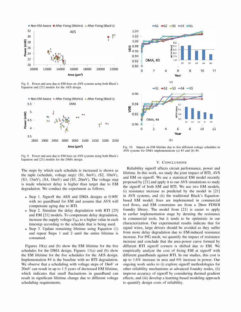
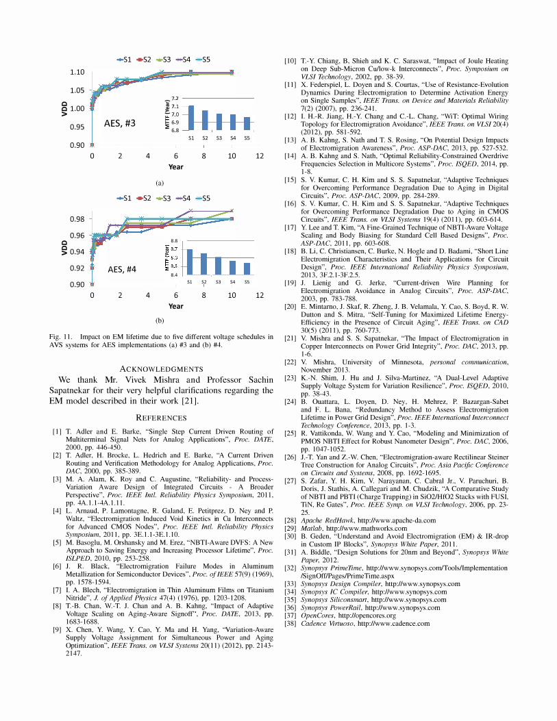
Figures 1O(a) and (b) show the EM lifetime for the five schedules for the DMA design. Figures l1(a) and (b) show the EM lifetime for the five schedules for the AES design. Implementation #4 is the baseline with no BTl degradation. We observe that a scheduling with voltage steps of 18mV or 20mV can result in up to 1.5 years of decreased EM lifetime, which indicates that small fluctuations in guardband can result in significant lifetime change due to different voltage scheduling requirements.
(b)
Fig. 10. Impact on EM lifetime due to five different voltage schedules in AVS systems for DMA implementations (a) #3 and (b) #4.
V. CONCLUSIONS
Reliability signoff affects circuit performance, power and lifetime. In this work, we study the joint impact of BTl, AVS and EM on signoff. We use a statistical EM model recently proposed by [21] and apply it to our AVS simulations to study the signoff of both EM and BTL We use two EM models, (i) resistance increase as predicted by the model in [21] in AVS systems, and (ii) the traditional Black's Equationbased EM model; fixes are implemented in commercial tool flows, and EM constraints are from a 28nm FDSOI foundry library. The model from [21] is easier to apply in earlier implementation stage by derating the resistance in commercial tools, but it tends to be optimistic in our characterization. Our experimental results indicate that for signal wires, large drivers should be avoided as they suffer from more delay degradation due to EM-induced resistance increase. For PIG mesh, we quantify the impact of resistance increase and conclude that the area-power curve formed by different BTl signoff corners is shifted due to EM. We empirically analyze the cost of fixing EM at signoff with different guard bands against BTL In our studies, this cost is up to 1.6% increase in area and 6% increase in power. Our ongoing work seeks to (i) explore sign off methodologies for other reliability mechanisms at advanced foundry nodes, (ii) improve accuracy of signoff by considering thermal gradient effects, and (iii) develop a learning-based modeling approach to quantify design costs of reliability.
1.10
1.05
§ 1.00 >
0.95
0.90 0
0.98
0.96 c §! 0.94
0.92
0.90 0
�Sl �S2 �S3 �S4 �S5
AES,#3
2 4
�Sl �S2
AES,#4
2 4
-" E til : I I
Sl S2 S3
6 8 Year
(a)
�S3 �S4 ...,.S5
.. � f : : ] 11 8.4 , 51 52 53
6 8 Year
(b)
I I S4 S5
10 12
I , I ,
54 55
10 12
Fig. II. Impact on EM lifetime due to five different voltage schedules in AVS systems for AES implementations (a) #3 and (b) #4.
ACKNOW LEDGMENTS
We thank Mr. Vivek Mishra and Professor Sachin Sapatnekar for their very helpful clarifications regarding the EM model described in their work [21].
REFERENCES
[1] T Adler and E. Barke, "Single Step Current Driven Routing of Multiterminal Signal Nets for Analog Applications", Proc. DATE, 2000, pp. 446-450.
[2] T Adler, H. Brocke, L. Hedrich and E. Barke, "A Current Driven Routing and Verification Methodology for Analog Applications, Proc. DAC, 2000, pp. 385-389.
[3] M. A. Alam, K. Roy and C. Augustine, "Reliability- and ProcessVariation Aware Design of Integrated Circuits - A Broader Perspective", Proc. IEEE Inti. Reliability Physics Symposium, 2011, pp. 4A. 1.1-4A. 1.1 I.
[4] L. Arnaud, P. Lamontagne, R. Galand, E. Petitprez, D. Ney and P. Waltz, "Electro migration Induced Void Kinetics in Cu Interconnects for Advanced CMOS Nodes", Proc. IEEE IntI. Reliability Physics Symposium, 2011, pp. 3E.1.1-3E.1.10.
[5] M. Basoglu, M. Orshansky and M. Erez, "NBTl-Aware DVFS: A New Approach to Saving Energy and Increasing Processor Lifetime", Proc. ISLPED, 2010, pp. 253-258.
[6] J. R. Black, "Electromigration Failure Modes in Aluminum Metallization for Semiconductor Devices", Proc. of IEEE 57(9) (1969), pp. 1578-1594.
[7] I. A. Blech, "Electromigration in Thin Aluminum Films on Titanium Nitride", 1. of Applied Physics 47(4) (1976), pp. 1203-1208.
[8] T-B. Chan, W-T J. Chan and A. B. Kahng, "Impact of Adaptive Voltage Scaling on Aging-Aware Signoff", Proc. DATE, 2013, pp. 1683-1688.
[9] X. Chen, Y. Wang, Y. Cao, Y. Ma and H. Yang, "Variation-Aware Supply Voltage Assignment for Simultaneous Power and Aging Optimization", IEEE Trans. on VLSI Systems 20(11) (2012), pp. 2143-2147.
[10]
[11]
[l2]
[13]
[l4]
[lS]
[16]
[17]
[l8]
[l9]
[20]
[21]
T-Y. Chiang, B, Shieh and K. C. Saraswat, "Impact of Joule Heating on Deep Sub-Micron Cullow-k Interconnects", Proc. Symposium on VLSI Technology, 2002, pp. 38-39. X. Federspiel, L. Doyen and S. Courtas, "Use of Resistance-Evolution Dynamics During Electromigration to Determine Activation Energy on Single Samples", IEEE Trans. on Device and Materials Reliability 7(2) (2007), pp. 236-241. I. H.-R. Jiang, H.-Y. Chang and c.-L. Chang, "WiT: Optimal Wiring Topology for Electromigration Avoidance", IEEE Trans. on VLSI20(4) (2012), pp. 581-592. A. B. Kahng, S. Nath and T S. Rosing, "On Potential Design Impacts of Electromigration Awareness", Proc. ASP-DAC, 2013, pp. 527-532. A. B. Kahng and S. Nath, "Optimal Reliability-Constrained Overdrive Frequencies Selection in Multicore Systems", Proc. ISQED, 2014, pp. 1-8. S. V. Kumar, C. H. Kim and S. S. Sapatnekar, "Adaptive Techniques for Overcoming Performance Degradation Due to Aging in Digital Circuits", Proc. ASP-DAC, 2009, pp. 284-289. S. V. Kumar, C. H. Kim and S. S. Sapatnekar, "Adaptive Techniques for Overcoming Performance Degradation Due to Aging in CMOS Circuits", IEEE Trans. on VLSI Systems 19(4) (2011), pp. 603-614. Y. Lee and T Kim, "A Fine-Grained Technique of NBTI-Aware Voltage Scaling and Body Biasing for Standard Cell Based Designs", Proc. ASP-DAC, 2011, pp. 603-608. B. Li, C. Christiansen, C. Burke, N. Hogle and D. Badami, "Short Line Electromigration Characteristics and Their Applications for Circuit Design", Proc. IEEE International Reliability Physics Symposium, 2013, 3F.2.1-3F.2.5. J. Lienig and G. Jerke, "Current-driven Wire Planning for Electromigration Avoidance in Analog Circuits", Proc. ASP-DAC, 2003, pp. 783-788. E. Mintarno, J. Skaf, R. Zheng, J. B. Velamala, Y. Cao, S. Boyd, R. W Dutton and S. Mitra, "Self-Tuning for Maximized Lifetime EnergyEfficiency in the Presence of Circuit Aging", IEEE Trans. on CAD 30(5) (2011), pp. 760-773. V. Mishra and S. S. Sapatnekar, "The Impact of Electromigration in Copper Interconnects on Power Grid Integrity", Proc. DAC, 2013, pp. 1-6.
[22] V. Mishra, University of Minnesota, personal communication, November 2013.
[23] K.-N. Shim, J. Hu and J. Silva-Martinez, "A Dual-Level Adaptive Supply Voltage System for Variation Resilience", Proc. ISQED, 2010, pp. 38-43.
[24] B. Ouattara, L. Doyen, D. Ney, H. Mehrez, P. Bazargan-Sabet and F. L. Bana, "Redundancy Method to Assess Electromigration Lifetime in Power Grid Design", Proc. IEEE International Interconnect Technology Coriference, 2013, pp. 1-3.
[25] R. Vattikonda, W Wang and Y. Cao, "Modeling and Minimization of PMOS NBTl Effect for Robust Nanometer Design", Proc. DAC, 2006, pp. 1047-1052.
[26] J.-T Yan and Z.-W. Chen, "Electromigration-aware Rectilinear Steiner Tree Construction for Analog Circuits", Proc. Asia Pacific Coriference on Circuits and Systems, 2008, pp. 1692-1695.
[27] S. Zafar, Y. H. Kim, V. Narayanan, C. Cabral Jr., V. Paruchuri, B. Doris, J. Stathis, A. Callegari and M. Chudzik, "A Comparative Study of NBTI and PBTl (Charge Trapping) in Si02/Hf02 Stacks with FUSI, TiN, Re Gates", Proc. IEEE Symp. on VLSI Technology, 2006, pp. 23-25.
[28] Apache RedHawk, http://www.apache-da.com [29] Matlab, http://www.mathworks.com [30] B. Geden, "Understand and Avoid Electromigration (EM) & IR-drop
in Custom IP Blocks", Synopsys White Paper, 2011. [31] A. Biddle, "Design Solutions for 20nm and Beyond", Synopsys White
Paper, 2012. [32] Synopsys PrimeTime, http://www.synopsys.comlTools/Implementation
ISignOfflPages/PrimeTime.aspx [33] Synopsys Design Compiler, http://www.synopsys.com [34] Synopsys IC Compiler, http://www.synopsys.com [35] Synopsys Siliconsmart, http://www.synopsys.com [36] Synopsys PowerRail, http://www.synopsys.com [37] Open Cores, http://opencores.org [38] Cadence Virtuoso, http://www.cadence.com