
High frequency pulsed electromigration
202
HIGH FREQUENCY PULSED ELECTROMIGRATION By DAVID WAYNE MALONE A DISSERTATION PRESENTED TO THE GRADUATE SCHOOL OF THE UNIVERSITY OF FLORIDA IN PARTIAL FULFILLMENT OF THE REQUIREMENTS FOR THE DEGREE OF DOCTOR OF PHILOSOPHY UNIVERSITY OF FLORIDA 1997
Transcript of High frequency pulsed electromigration
HIGH FREQUENCY PULSED ELECTROMIGRATION
By
DAVID WAYNE MALONE
A DISSERTATION PRESENTED TO THE GRADUATE SCHOOLOF THE UNIVERSITY OF FLORIDA IN PARTIAL FULFILLMENT
OF THE REQUIREMENTS FOR THE DEGREE OFDOCTOR OF PHILOSOPHY
UNIVERSITY OF FLORIDA
1997

ACKNOWLEDGMENTS
First and foremost, I must thank my wife, Ming Rong. I have relied upon
her support and sacrifice above all else over the past four years, while our family
life has been on hold. Together with our daughter, Lili, we can finally proceed.
I thank my mother, Judy, and my father, Wayne, for their endless support.
It was my fortune to have, in addition to great parents, a father who is an expert
in rf design. His help in the design and construction of the electromigration test
apparatus was invaluable, as was the generosity of Skydata, Inc.
Dr. Rolf Hummel has been a consistent source of confidence. It was my
contact with him as an undergraduate that led to my return to the University of
Florida for graduate work, and many of his philosophies will go with me after I
leave. I thank him for his guidance and for his belief in me.
Funding for this work was provided by Motorola, Inc., through their
Advanced Products Research and Development Laboratory at Austin, TX. I
gratefully acknowledge their support. Several people at Motorola should be
mentioned by name. At the top of the list is H. Kawasaki, who directed our
relationship with Motorola. Test samples were provided by M. Fernandes,
C. Lee, M. Gall, and R. Hernandez. R. Hernandez also performed SEM work.
Finally, I acknowledge Drs. R. T. DeHoff, R. M. Park, R. K. Singh, and
T. J. Anderson for their service on my faculty committee.
ii

TABLE OF CONTENTS
ACKNOWLEDGMENTS ii
ABSTRACT v
INTRODUCTION 1
Overview 1
The Integrated Circuit and Electromigration 4
Motivation 1
1
BACKGROUND 13
Foundations 13
Groundwork and Prior Research 34
Modern Implications 60
Pulsed Electromigration 61
Summary 77
SETUP AND PROCEDURE 79
Overview 79
Test Apparatus Performance Goals 79
Design Issues 81
Summary of Test Apparatus 84
Test Stripes 88
Test Procedure 90Data Gathering and Analysis 90
Test Conditions 92
RESULTS AND DISCUSSION 94
Overview 94Resistance Plots and Optical Micrographs 95Lifetime Data 126Relationships Between Lifetime, Pulse Frequency and Duty Cycle .. 147Further Discussion 157
SUMMARY AND CONCLUSION 1 65

SUGGESTIONS FOR FUTURE WORK 169
APPENDIX 171
Test Apparatus 171
Further Discussion of Design and Procedure 183
REFERENCES 186
BIOGRAPHICAL SKETCH 194
Abstract of Dissertation Presented to the Graduate School
of the University of Florida in Partial Fulfillment of the
Requirements for the Degree of Doctor of Philosophy
HIGH FREQUENCY PULSED ELECTROMIGRATION
By
DAVID WAYNE MALONE
May, 1997
Chairman: Dr. Rolf E. HummelMajor Department: Materials Science and Engineering
Electromigration life tests were performed on copper-alloyed aluminum
test structures that were representative of modern CMOS metallization schemes,
complete with Ti/TiN cladding layers and a tungsten-plug contact at the cathode.
A total of 18 electrical stress treatments were applied. One was a DC current of
15 mA. The other 17 were pulsed currents, varied according to duty cycle and
frequency. The pulse amplitude was 15 mA (-2.7 x 10⁶A/cm
2
) for all treatments.
Duty cycles ranged from 33.3% to 80%, and frequencies fell into three rough
ranges - 100 KHz, 1 MHz, and 100 MHz. The ambient test temperature was
200 °C in all experiments. Six to 9 samples were subjected to each treatment.
Experimental data were gathered in the form of test stripe resistance
versus time, R(t). For purposes of lifetime analysis, "failure" was defined by the
criterion R(t)/R(0) = 1.10, and the median time to failure, tso, was used as the
primary basis of comparison between test groups.
v

It was found that the dependence of t5o on pulse duty cycle conformed
rather well to the so-called "average current density model" for duty cycles of
50% and higher. Lifetimes were less enhanced for a duty cycle of 33.3%, but
they were still considerably longer than an "on-time" model would predict. No
specific dependence of tso on pulse frequency was revealed by the data, that is,
reasonably good predictions of tso could be made by recognizing the dominant
influence of duty cycle.
These findings confirm that IC miniaturization can be more aggressively
pursued than an on-time prediction would allow. It is significant that this was
found to be true for frequencies on the order of 100 MHz, where many present
day digital applications operate.
Post-test optical micrographs were obtained for each test subject in order
to determine the location of electromigration damage. The pulse duty cycle was
found to influence the location. Most damage occurred at the cathode contact,
regardless of treatment conditions, but there was an increased incidence of
damage farther downwind with decreasing duty cycle. This tendency and the
deviation from the average current density model for small duty cycles were
explained in terms of the Blech length, its dependence on microstructure and
duty cycle, and its impact on the relative rates of damage and recovery.
vi
INTRODUCTION
Overview
Electromigration, a process whereby an electric current "erodes" the
conductor that carries it, is commonly recognized as a failure mechanism in
integrated circuits. The on-chip interconnections of an integrated circuit are
particularly vulnerable to such a process because they are microscopic in size,
and failure occurs if one of them becomes excessively resistive or discontinuous
at some point because of localized thinning or voiding. Although it was not
immediately identified as electromigration, this mode of failure was discovered
shortly after the inception of the integrated circuit (IC) in the early 1960s, and it
has continued to be a reliability issue with IC manufacturers ever since.
Recent interest in electromigration research is closely related to the
incessant drive to place more circuit functions on a chip. This drive, which seeks
to increase device packing densities, has been carried out largely by reducing
the sizes of circuit features. For example, it has been a common practice to
reduce the widths of interconnections whenever process technologies allow it.
Such practice often endangers reliability, though, because when the widths of
interconnections are scaled down, it is not always possible to scale the current
down in proportion. Those interconnections must then carry a larger amount of
current per unit of interconnect cross section, that is, they must carry a larger
1
2
current density. Electromigration is then more likely. Future battles with
electromigration are likely to be a by-product of IC miniaturization.
In practice, the ability of a particular IC interconnect structure to resist
electromigration is predicted by performing experiments on specially prepared
test structures. A group of test structures is subjected to some steady DC
current, and the temperature is elevated in order to accelerate the damage
process. Some measure of electromigration damage is monitored and is
reported for all appropriate variations of conditions.
The traditional reliability test employs a steady DC current as the primary
treatment variable. It is important, however, to realize that a steady DC current
may not be particularly relevant. Many of the interconnections on a typical
integrated circuit might, in actual operation, carry pulsed currents, alternating
currents, or other less destructive current waveforms. The reliability of these
interconnections will be underestimated if no adjustment is made to the DC test
or its interpretation. This is acceptable if the prediction falls within specifications
anyway, but if it does not, the true reliability of these interconnections must be
further investigated.
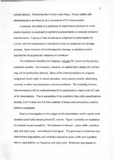
Such an investigation is the subject of this dissertation, which reports work
directed specifically toward pulsed DC current. Figure 1 provides an illustration
of a pulsed current waveform. The features of interest ~ pulse width, repetition
rate, and duty cycle - are defined in the figure. The goal was to determine how
interconnect degradation and reliability depend on pulse width and repetition
rate or, equivalently, on frequency and duty cycle. Emphasis was placed on
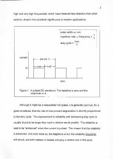
3
high and very high frequencies, which have received less attention from other
workers, despite their practical significance to modern applications.
pulse width => t-on
repetition rate => frequency =
duty cycle =t-on
currentperiod, T
At-on —
»
t-off
o i 1 1 —I 1 1 >
time
Figure 1 . A pulsed DC waveform. The baseline is zero and the
amplitude is A.
Although it might be a reasonable first guess, it is generally not true, for a
given amplitude, that the rate of interconnect degradation is directly proportional
to the duty cycle. The improvement in reliability with decreasing duty cycle is
usually found to be larger than such a relation would predict. The reliability is
said to be "enhanced" when the current is pulsed. The reason that the reliability
is enhanced, and even more so, the degree to which the reliability should be
enhanced, are both matters of debate and play a central role in this work.

4
The Integrated Circuit and Electromigration
An integrated circuit (IC) is that special type of electronic circuit commonly
known as a "microchip." The computer chip is a familiar example. True to its
name, an IC is, in fact, an electronic circuit that is consolidated (integrated) onto
a thin substrate such that it appears to be a small piece (chip) of solid material.
The circuitry on a chip is microscopic, a feat which is made possible by the thin
film techniques that are used to fabricate it. Although it is this microscopic size
that makes an IC such a marvel of computing power, it is also responsible for the
vulnerability of an IC to the effects of electromigration.
The microscopic thin film "wires" that connect the components on a chip
are usually called "interconnections" or "interconnects." Sometimes, the term
"metallization" is used, not only in reference to the interconnections themselves,
but also in reference to the process of fabricating them. Most interconnections
are, in fact, made of metallic alloys or compounds, and any metal film that is
deposited during the course of IC fabrication is likely done so for this purpose.
Copper-alloyed aluminum is the predominant material used for interconnections,
but other metals, primarily titanium and tungsten, serve important supplementary
roles in most metallization schemes.
Electromigration can be viewed roughly as an electronic form of erosion,
because it takes place when the current running through any particular part of a
circuit is large enough to push atoms down the length of an interconnect. Just
as wind blows sand from one portion of a beach and piles it up in other locations
downwind, the flowing electrons that comprise an electric current may push

5
material away from some portions of an IC interconnect and pile it up in other
regions "downwind." The rough nature of this analogy does not detract from the
introductory picture that it provides, but it will need some clarification later.
Nonetheless, a segment of interconnect may be broken open at a spot upwind,
where material is depleted by the current. Conduction is lost, and the result is
failure of the circuit. Downwind accumulation of material can be a problem, as
well. It often appears as a mound called a "hillock." Sometimes, when enough
compression is built up downwind, material may be extruded out from the bulk of
the interconnect, to form what is called an "extrusion" or a "whisker." If a hillock
or whisker is large enough that it makes contact with an adjacent interconnect
line, then the resulting electrical short will likely constitute a failure of the circuit.
A depiction of electromigration damage is presented in Figure 2. The
figure depicts a conductor with a (-) terminal, a (+) terminal, and the resulting
direction of electron flow. It could be taken to be an IC interconnect or a test
structure. An electromigration-induced void is shown at the upwind end of the
conducting strip, and hillocks are shown at the downwind end.
Figure 2. Electromigration-induced degradation of an interconnect.

6
Because of the analogy to erosion, and because the electric current is a
flow of electrons, the force that causes electromigration is sometimes called the
"electron wind" force. An electron wind force is present, and electromigration is
possible, in any wire or material that is made to pass an electric current. For
example, it has been observed in DC-powered light bulb filaments, and it has
been observed in liquid metals. In fact, it is a potentially useful phenomenon for
purifying metals. In the microelectronics industry, electromigration is a detriment
to business, and its prevention has been an issue for about three decades.
Even though it is just one of many reliability issues associated with
integrated circuits, electromigration is particularly relevant with regard to long
term reliability. This "electronic erosion" process is normally quite slow, and it is
usually noticed only after years of device operation. Electromigration failure
cannot be screened-out by inspection or burn-in before delivery the way that
some processing defects can. The only way to avoid electromigration-related
failures in the field is to eliminate the occurrence of electromigration or to slow it
down enough that its effects are not likely to be seen before the product is
discarded. This effort starts with an understanding of why electromigration
occurs and how its occurrence depends on the materials properties of a given
interconnection and the conditions to which the interconnection is subjected.
Research has placed special emphasis on the following variables:
1 . Current density
2. Temperature
3. Chemical composition
4. Microstructure
5. Macrostructure

7
The first two of these variables, current density and temperature, are the
conditions to which the interconnect may be subjected. They are the true
"variables" per se. Since electric current is the erosive agent responsible for
electromigration, it is certainly the critical variable. The rate of electromigration
is expected to increase as the magnitude of the current density increases. The
temperature should be important, as well, because it determines how vigorous
the atomic vibrations are, and therefore how mobile the atoms are, in a solid.
Higher temperatures should encourage faster migration rates.
The final three variables in the above list are chemical composition,
microstructure, and macrostructure, which are those physical attributes of the
interconnect that influence the manner and extent of atom migration, given some
current density and temperature. The effort to produce reliable interconnects
has been concentrated largely on these factors.
Chemical composition is important presumably because such properties as
density, atomic weight, and bond strength determine how well the atoms of a
material resist displacement from their positions. The more dense and strongly
bound a material is, the more resistant one might expect it to be to disruption by
the electron wind force.
The rate at which atoms are pushed by the electron wind should, it seems,
be determined by the degree to which the given chemical composition can
oppose the active influences of current density and temperature. This is
essentially correct, but the rate of migration, by itself, does not determine the
rate of damage . It was stated earlier that the electron wind damages an

8
interconnect by pushing material away from some regions upwind and by piling
material up in other regions downwind. So, damage shows itself as localized
depletions or accumulations of material. In order for material to be depleted
from or accumulated at a particular location, there must be a discontinuity or
divergence in the migration rate at that location. Such a divergence could be
caused by a local variation of the current density or temperature. Even when the
current density and temperature are uniform, however, rate divergences will
certainly exist, because virtually all materials have a microstructure, which is the
fourth variable in the above list.
The microstructure of a material is derived from such structural features as
grain size, grain size distribution, and phase distribution, which affect the interior
uniformity of a piece of material. If a microstructure contains some distribution of
a second phase, for example, then it is not uniform chemically. Migration should
proceed more readily in the less dense, less strongly bound phase than it does
in the other, so long as the current density is uniform throughout. The resulting
variation in migration rate from one phase to the next requires that material be
depleted from or accumulated at the boundary between those differing regions.
That boundary thus becomes a site of electromigration damage. Voids may be
formed at boundaries where material is depleted, and hillocks or whiskers may
be formed where material is accumulated. Another microstructural feature, the
grain boundary, is not such an obvious example of chemical inhomogeneity as is
a second phase, but it is chemically different from the interior of a grain. A grain
boundary is less dense and less strongly bound. So, electromigration should
occur more readily in a grain boundary than it does within the grains that it
separates. Localized depletion or accumulation is again the likely result. In
practice, grain boundary migration is the primary mode of damage.
So, if an interconnect does not contain such microstructural nonuniformities
as second phases or grain boundaries, no damage is expected, so long as the
current density and temperature are uniform. According to this reasoning, no
damage should occur within a single crystal interconnect, regardless of the
migration rate. Of course, there must be an infinite source of atoms at the
upwind end and an infinite sink at the downwind end in order to maintain the
steady state migration over time.
Normally, an interconnect configuration provides neither an infinite upwind
source of atoms nor an infinite downwind sink. This reality is related to the final
item in the above list - macrostructure. The macrostructure of an interconnect
includes such factors as size and shape, as well as the composite structure and
composition of the entire metallization scheme. For example, any interconnect,
on both ends, will ultimately make contact to a dissimilar material, such as an
electrode, or some kind of a splice along the way. There will always be at least
two sites, then, at which the migration rate is discontinuous, even when the
interconnect itself happens to be a single crystal.
The size and shape of an interconnect may also influence its susceptibility
to electromigration damage. For example, a void of some given size should be
more detrimental to a narrow, thin interconnect than it is to a wide, thick
interconnect. This is just a statistical effect, but geometry can also influence

10
damage kinetics by affecting the uniformity of current density and temperature.
For a given current, if the cross-sectional area is not uniform over the length of
an interconnect, then the current density is not uniform, either. A divergence in
current density produces a local divergence in migration rate. In addition, a
nonuniform current density is likely to produce a local temperature gradient,
which aggravates the rate divergence even further.
Studies of electromigration generally involve a systematic variation of some
or all of these five variables, where each variation is applied to a small group of
identical samples. Each sample is a specially designed test structure that is
chemically and structurally similar to an actual segment of interconnect. Even
though special considerations do go into the design of a test structure, it is
usually not much more than a microscopic strip of metal built onto a chip. It is
often called a "test stripe."
In order to monitor the electromigration behavior of a group of test stripes,
some appropriate measure is needed. A commonly utilized in situ measure is
electrical resistance. As material is redistributed during the course of
electromigration, the electrical resistance of a given test stripe will probably
change. If the stripe becomes thinner, or if it experiences localized depletions of
material, the resistance will increase. If the stripe ultimately breaks completely
open, then conduction is completely lost, and the resistance becomes infinite.
It has been mentioned that reliability tests must be accelerated by
subjecting test stripes to current densities and temperatures that are higher than
normal. The first order of business, then, in early work, was to determine the

11
dependence of electromigration on current density and temperature. A model
was needed to extrapolate test results for application in the field. With such a
model in hand, the other three variables - chemical composition, microstructure,
and macrostructure - could be more easily evaluated, as well.
Motivation
With the miniaturization afforded by recent IC metallization technologies,
electromigration is increasingly a significant reliability issue. The emerging
relevance of electromigration is mostly due to falling interconnection linewidths
and the elimination of contact overlap, in conjunction with the continued use of
aluminum-based interconnections. A key feature of present technologies, the
tungsten-filled contact via, seems to be an open invitation to electromigration
damage. Interconnect reliability is determined conclusively at this structural
discontinuity by the ability of the aluminum-copper alloy to endure an electron
wind. It seems advisable to avoid the use of such a structure, but the "tungsten
plug" is a key to producing "ultra high" levels of integration. In addition, it is not
possible to eliminate all similarly unfavorable structural features, anyway. A
compositional discontinuity is always present at the end of an interconnect,
whether that end is contacted to a tungsten plug or to a silicon device. This
vulnerability is unavoidable, so the adoption of sufficiently robust interconnect
materials is the surest way to minimize concerns about electromigration.
Industry is hesitant or unprepared to abandon copper-alloyed aluminum as
the primary constituent of IC interconnections. It is not certain when this fact will
12
become the downfall of efforts for miniaturization, but significant ground may be
gained in the meantime by ensuring that test models are as realistic as possible.
Specifically, it is preferable to utilize electromigration models that are tailored for
AC operation or pulsed DC operation whenever these more accurately represent
true circuit conditions. With regard to pulsed DC applications, such an effort is
based upon the dependence of interconnect reliability on pulse length and pulse
repetition rate. The accurate determination of this dependence will give circuit
engineers the opportunity to more fully utilize the limits of present metallization
schemes. Given the limitation of aluminum-copper alloys, the need for such
knowledge is great.
This study is most significant from a technological viewpoint, because the
information that it reveals is particularly relevant for IC designers who need to
predict the reliability of circuits that will carry pulsed currents. The practical
need for such information has been discussed.
The dependence of the rate of electromigration damage on the pulse duty
cycle and frequency is a reflection of the time-dependences of the associated
diffusion processes. This is fundamentally a scientific consideration, but it is
also inherently relevant in light of the computer industry's constant push for
faster processing speeds. As such, the high frequency regime is of particular
interest, but little work is reported in the literature for pulse frequencies greater
than 1 MHz. These issues were motivation for the present work.

BACKGROUND
Foundations
An introduction to the integrated circuit and electromigration was
presented in the previous chapter. The discussion included, in addition to basic
introductory remarks, a rather complete qualitative description of the significant
variables that determine electromigration behavior. Quantitative discussion is
saved for later. Further, the motivation for this work was revealed by identifying
the challenges associated with IC miniaturization and the resulting need for
accurate models when assessing the reliability of circuits that will carry pulsed
currents. Next is a discussion of the scientific basis for electromigration.
As a start to understanding why electromigration might occur in the first
place, it is helpful to consider the process of electrical conduction. This is a
reasonable starting point for revealing why electromigration is possible, and it
provides a basis for speculating on the form of any fundamental model that might
describe the process.
When an electric current is made to flow through a conductive material
under the force of an applied voltage, the charge carriers of which the current is
composed cannot avoid interaction with the atoms of the conducting material.
This interaction causes some resistance to the flow of current, and the
magnitude of the resistance determines the amount of current that can flow.
13

14
Electrical resistance can be viewed as a frictional force that opposes the
motion of electrons as they try to accelerate through a metal conductor under the
force of an applied voltage. At steady state, the accelerating force imposed by
the voltage and the resistive frictional force are equal in magnitude and opposite
in direction. There is no net acceleration of the conduction electrons as they
appear to attain some uniform terminal velocity similar to the manner in which a
skydiver reaches a terminal velocity when the force of the wind resistance
becomes equal to the force of gravity. This analogy appears to be reasonable,
but it works only when the electrons are viewed for their average motion. Taken
individually, the motions of electrons within a conductor, even those participating
in conduction, cannot be considered to be so uniform or so laminar as the
motion of a skydiver. Any given free electron can be moving in any direction,
and, according to the wave theory for electrons, the manner in which it interacts
with nearby atoms depends, at any moment, on the instantaneous positioning
and periodicity of those atoms. This much is true regardless of the external
conditions to which the conducting material is subjected. The electrons and
nearby atoms interact constantly in a random give and take fashion, and, at
thermal equilibrium, there is no net velocity displayed by either component in the
homogeneous system. The sum of all the individual electron velocities resolved
in any given direction is balanced by an equal sum resolved in the opposite
direction, so long as no voltage or other external force is imposed.
The effect of an applied voltage and the associated electrical force field is
just to divert the path of some electrons very slightly toward the direction of the

electrical force. This diversion is very small compared to the otherwise random
motions of electrons, but it represents, nonetheless, some net component of
velocity directed down the conductor. This is the apparent terminal velocity
mentioned earlier for steady state. The term "apparent" is used because this
velocity consists only of the small drift component that is superimposed on the
total electron velocity field, and, even though the magnitude of the drift velocity
of any particular electron is actually several orders of magnitude smaller than its
total speed, it is only the drift component that is observable. It is observed as an
electric current, and it delivers the electron wind force.
The friction-like resistance is not so uniform on the atomic scale, either. It
is associated not only with the simple physical impediment that the atoms of the
conductor present by their presence in the path of electron flow, but also with the
vibrational thermal energy that is distributed among the atoms. In fact, quantum
theory says that the simple physical barrier that the atoms seem to present will
not exist if the atoms remain stationary in a perfectly periodic arrangement. The
fact that the atoms of a solid are not stationary, but rather vibrate about some
equilibrium lattice position, in addition to the fact that they probably would not be
perfectly periodic even if they were stationary, accounts for the failure of an
electric current to flow unimpeded. The distribution of possible electron/atom
interactions is determined by the temperature-dependent distribution of lattice
vibrational energies.
Because of electrical resistance, then, a conduction electron cannot reach
the same drift speed in a piece of matter as it can if it is accelerated through the

16
same voltage in a vacuum. This deficit in speed shows up as a quantity of
energy dissipated among those interfering atoms that cause the deficit. That is,
if atoms exert an interference force on conduction electrons, then it must be that
those electrons exert a force on the atoms - the electron wind force. The drift
velocity represents a balance of these forces.
It is clear that the electron wind force delivers energy to the atoms of a
conducting medium. In fact, it can deliver enough energy to heat the material
considerably, even to its melting point. A more important consideration in the
present context, however, is what happens when the current is not so large as to
cause extreme heating, and the temperature is therefore far below the melting
point. Can atoms be pushed down the conductor by the electron wind at normal
circuit operating conditions? The answer is certainly "yes," but a consideration
of some quantitative facts might lead one to initially doubt such a claim. For this
purpose, consider the following quantities for an aluminum conductor, held at a
temperature of 100 °C and carrying a current density of 1x1
0
6A/cm
2:
1 . Energy required to move an atom: ~ 0.2 to 1 eV2. Thermal energy of an average atom: ~ 0.04 eV
3. "Wind" energy per electron/atom interaction: < 1 x 1
0~5 eV
It does not seem that there is any chance for a conduction electron to push an
aluminum atom to a new position in the crystal. The typical drift content of a
conduction electron carries less than 1x10"5 eV of energy into an electron/atom
interaction, and it takes about 0.2 eV to 1 eV to move an atom to an adjacent
position, depending on the nature of that position.

17
So, how can electromigration occur? The answer lies in the knowledge
that atoms already contain some quantity of thermal energy anyway, and they
may migrate through bulk crystals quite readily by the process of diffusion. At
first glance, this also appears to be questionable, because the average thermal
energy per aluminum atom in this example is only about 0.04 eV. It is not the
average atom, however, that moves by diffusion. The thermally induced
vibrational energy in a crystal is distributed quite broadly among the atoms, and,
although the average atom possesses an energy of only 0.04 eV, there is some
fraction of atoms whose energy will equal or exceed 1 eV. So, this fraction, at
any moment, can move to adjacent locations if those locations are vacant.
The primary requirements for an atom to move to a neighboring location
within a piece of matter are that it obtain the appropriate energy and that there
be a space for it there. Within the bulk of a crystal grain, such a space may be
provided by a lattice vacancy. There is also space on free surfaces, interfaces,
and boundaries between individual crystal grains. When the moving species is
substantially smaller than the atoms of the host lattice, room may be available
between regular lattice sites. There is always some quantity of vacant lattice
sites, there is always some number of interfaces or free surfaces, and there is
almost always an ample number of grain boundaries within a piece of matter.
This is certainly true of the aluminum thin films of which integrated circuit
interconnect is composed.
At normal temperatures, then, diffusion always occurs. Any given atom,
or even more assuredly, any given vacancy, may move a considerable distance

through the lattice over time. This movement has no real effect on the apparent
condition of a piece of material, however, if the material is homogeneous and
there is no other influence, because for whatever direction and distance any
particular atom migrates through a crystal, there will be, on average, another
atom that migrates an equal distance in the opposite direction. Diffusion causes
some net change in the arrangement of atoms only if there is some bias imposed
on the apparent direction of the diffusive process. That is, there must be some
so-called "driving force."
The most commonly treated driving force results from a concentration
gradient, on which the traditional study of diffusion is based. For example, the
science of diffusion and simple intuition will predict that if a piece of material is
somehow made to have most of its vacancies located toward one of its ends at a
given moment, then over time the vacancies will redistribute toward a more
uniform arrangement. The influence that causes this rearrangement is not really
a force in the physical sense, rather it is derived from the statistical bias
associated with the vacancy concentration gradient that was set up. The end
with most of the vacancies can "send" more vacancies to the other end than the
other end can "give" back. So, the vacancy concentration tends to even out.
The effect of the concentration gradient is equivalent to a driving force, so it is
considered as such.
Other driving forces are commonly encountered as well. A temperature
gradient provides a kind of directional bias in which atoms tend to move from
hotter regions toward cooler regions. A stress gradient will assist migration
19
away from regions of compression and toward regions of tension. The driving
force for electromigration is provided by the electron wind. It is important to
stress, however, that none of these driving forces cause diffusion, they only
impose a bias on the apparent direction of the basic diffusive process. They
only influence the direction toward which the net change will occur. Diffusion is
caused by "thermal activation." This distinction requires that the comparison
made earlier between electromigration and erosion not be taken too literally.
The thermal content of a piece of material causes each of its atoms to
vibrate about some average position, its lattice position, at a frequency between
1012and 10
13per second. The period of a lattice vibration is thus 10"13 to 10"12
seconds, and the smallest moment during which a thermally induced event may
occur is about this length of time. For example, an atom that hops from its lattice
position to a vacant position next to it does so because it has gained sufficient
kinetic energy to make such a hop, and it has gained that energy during a
moment that is roughly 10~13 to 10"12 seconds long. Each successive interval of
time of this approximate length provides a new chance for an atom to obtain the
kinetic energy to engage in some process, such as lattice hopping or chemical
reaction. Since it is this period of time during which an atom "attempts" to do
something, the reciprocal of this time period is sometimes called the attempt
frequency. In mathematical terms, the fraction of attempts that are successful is
equivalent to the probability that any given attempt is successful. There is also
an equivalence between probability and concentration. For example, the
probability that some lattice position is vacant will be reflected directly by the

concentration of vacant lattice sites in the material. The terms "fraction,"
"concentration," and "probability" are interchangeable concepts.
A discussion of thermal activation can be attempted with reference to
Figure 3. This figure is a two-dimensional depiction of several atoms in a close-
packed arrangement. Atom A is chosen as a candidate to move to the adjacent
vacant site of Figure 3(a). In order for this atom to move to the vacant site, it
must push past the repulsion of the two shaded atoms and escape the attraction
of the other three neighbors. The inherent thermal content of the material may,
at some moment, randomly provide the required kinetic energy. If the atom, on
some given attempt, gains just enough momentarily directed thermal energy that
it just reaches the so-called "saddle point" halfway between its starting position
and the vacant position, as depicted in Figure 3(b), it is said to be "thermally
activated" for diffusion. The quantity of energy required for this activation is
called the "activation energy." If this quantity of energy, this quantity exactly, is
gained by the atom, so that it just reaches the saddle point, then it has a 50%
chance of dropping back to where it was and a 50% chance of continuing
(a) (b)
Figure 3. Activation of an atom for diffusion.
(a) Atoms surrounding a vacancy.
(b) Atom A is activated and sits at the saddle point.

21
forward into the originally vacant site if there is no other driving influence. The
same type of consideration applies to atom B and all other atoms next to the
vacancy if any happen to reach the activated state at any moment. With no
other influence, the average vacancy has an equally good chance of exchanging
positions with any one of its neighbor atoms as it does with any other.
When an electric current is passed through the material, there is another
influence - the electron wind. There is some chance that while an atom is in the
saddle position a conduction electron will deliver a push. As small as this push
is, the atom is nonetheless rendered more likely to move parallel to the electron
flow than it is to move the opposite way. For example, the activated atom A in
Figure 4(a) is biased slightly toward position 2. Likewise, the activated atom B
in Figure 4(b) is biased toward position 3.
(a) (b)
Figure 4. Activated atoms in the presence of an electron current.
(a) Atom A will most likely settle into position 2.
(b) Atom B will most likely settle into position 3.
The activated atom is apparently the focus of directionally biased diffusive
processes such as electromigration. In fact, it is the focus of the basic diffusion
mechanism itself. This is so because an atom that receives more than the

22
activation energy as it approaches the saddle point wiH pass through that point
and into the associated vacancy. An atom that receives less than the activation
energy will drop back into its starting position. The activated state is the pivotal
condition for an atom. This is true with or without an electron wind, but the
electron wind influences the outcome.
The rate of electromigration (or any diffusive process) is thus related to
the quantity of activated atoms at any moment, because this quantity determines
how many pivotal candidates there are for migration at that moment. It is widely
accepted that the fraction of atoms that possesses the energy required for
activation is proportional to exp(-Ea/kT), where Ea is the activation energy, T is
the temperature, and k is a constant known as Boltzmann's constant.
Implicit in the discussion so far has been the assumption that there is a
vacancy adjacent to the candidate atom. For most atoms in the bulk, however,
there is not a neighboring vacancy. An atom can be activated for diffusion only if
it gains sufficient energy and there is room for it to move, so the concentration of
vacancies is important in this analysis. This concentration is proportional to
exp(-Hv/kT), where Hv is the enthalpy for the formation of a vacancy. The
probability that an atom will gain sufficient energy for activation and have a
neighboring vacancy is the product of the probabilities for each condition alone.
This probability, rA , thus follows the proportionality given by
(1)

23
The quantity (Ea + Hv) is usually given a new symbol, Q, which is taken as the
activation energy for diffusion that accounts for both the energy requirement and
the neighboring vacancy requirement. The rate at which atoms are activated for
diffusion is thus proportional to exp(-Q/kT). The activation energy, Q, depends
on the material.
With respect to electromigration, the rate of activation is just part of the
story. Another part is related to the degree of directional bias, that is, the driving
force, imposed by the electron wind. The probability that a conduction electron
will interact with an atom while it is activated is expected to be proportional to the
rate at which electrons are conducted past any given point in the material, which
is equivalent to saying that this probability is proportional to the magnitude of the
electric current. The rate of electromigration should then be proportional to the
magnitude of the current for a specific piece of material and proportional to the
amount of current per unit of cross-sectional area (the current density) in the
general case.
An expression that relates current density and temperature to the rate of
electromigration can be proposed with the results of the preceding discussion.
The probability that a particular atom will become activated for migration at a
particular moment and will receive a push from a conduction electron while it is
activated, is given by the product of the probabilities for each event alone. The
probability of the former, as already mentioned, is proportional to exp(-Q/kT).
The probability of the latter is proportional to the current density, j. So, the total
24
probability that an atom migrates by an electron wind-assisted mechanism, rem,
is given by the proportionality
rem <x j-exp (2)
The rate of atomic migration should be directly proportional to rem , so this
expression is likely to be present, in some form, in any model that predicts the
rate of electromigration as a function of temperature and current density.
Some basics about the electron wind force, diffusion, and how the two
combine to create the phenomenon known as electromigration have now been
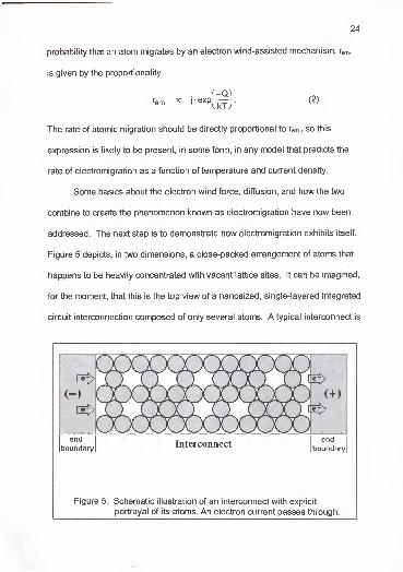
addressed. The next step is to demonstrate how electromigration exhibits itself.
Figure 5 depicts, in two dimensions, a close-packed arrangement of atoms that
happens to be heavily concentrated with vacant lattice sites. It can be imagined,
for the moment, that this is the top view of a nanosized, single-layered integrated
circuit interconnection composed of only several atoms. A typical interconnect is
(-)
aXXXXX(+)
end
boundaryInterconnect
endboundary
Figure 5. Schematic illustration of an interconnect with explicit
portrayal of its atoms. An electron current passes through.
25
really about one micrometer wide, one micrometer thick, and many micrometers
long, so this overly small picture is used only for demonstration.
The gray area on each end of the interconnect in Figure 5 can represent
some kind of a terminal, such as a contact pad, a contact to a device, or a splice
of some type. It may or may not be composed of the same material as the
interconnect. The atoms are not explicitly depicted in these regions because the
specific nature of the boundaries is left unknown for the moment. Various types
of boundaries can be considered. The interconnect itself is assumed to be any
good conductor. It is also indicated in the diagram that an electron current flows
from the negative contact toward the positive contact. The figure represents an
atom arrangement at time zero, when current has just been applied and no
electromigration has yet taken place.
Electromigration damage, we know, is not caused so much by the atomic
migration itself as it is by the presence of some nonuniformity or divergence in
the rate of migration. If the rate of migration varies from one region to the next,
then material will either be accumulated or depleted at a point between the two
regions. This is what produces the observable damage. So, in the situation
depicted by Figure 5, the electromigration behavior of the interconnect is
dependent to a large extent on whether the end boundaries are good sources
and/or sinks for atoms and vacancies. If they happen to be highly resistant to
electron wind-induced migration, then they act neither as sources nor sinks. The
interconnect can then be treated as an isolated entity, because its atoms and
vacancies are confined to the area between the two boundaries. If the
26
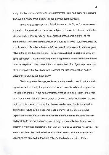
interconnect itself is not so resistant to electromigration, then the atoms will tend
to drift toward the positive end, and the vacancies will drift toward the negative
end. Since atoms cannot pass into the positive end boundary and vacancies
cannot pass into the negative end boundary for this particular scenario, the
drifting vacancies accumulate at the negative end and atoms accumulate at the
positive end of the interconnect. The accumulation of vacancies will likely
produce a void. Figure 6, depicts such a result.
(-) void (^t^][)i](^j(^](. X AJ? (+)
Figure 6. The interconnect of Figure 5 after electromigration has
caused a redistribution of atoms. The accumulation of
vacancies at the negative end has led to a void.
When either or both of the end boundaries are good sinks or sources for
atoms and/or vacancies, then the behavior of the interconnect may be different.
The susceptibility of the end boundaries to electromigration, relative to that for
the interconnect, will ultimately determine the outcome. Suppose that the
negative boundary region is some type of contact area that happens to be
reasonably susceptible to electromigration, which may be the case, for example,
if it is made of aluminum or copper. If the positive end boundary is still resistant
to electromigration and therefore does not accept atoms or provide vacancies,

27
then atoms will still accumulate at that end, but there will now be an additional
supply of atoms fed from the negative contact region by the electron wind. This
is depicted in Figure 7(a) for some intermediate arrangement of atoms after a
short time into the course of electromigration. Figure 7(b) shows a possible
arrangement at a later time. The darker shaded atoms are those that have been
fed in from the negative end boundary. So long as this region provides atoms
(a)
(") OC02020jGOGO (+)
UUUUUUUUUUUUiatom fed from (\ Interconnect
^
—
/ (-) contact \ ^ Al atom
(b)
(-) OCXXXXXXXXXjO (+)
Figure 7. Electromigration behavior when the (-) boundary is a goodsource of atoms and the (+) boundary is not a good sink.
(a) Some short time into the electromigration process.
(b) Some time later.
and accepts vacancies as fast as these species drift through the interconnect,
the result is quite different from the behavior shown in Figure 6. The vacancies

28
will eventually be swept out through the left end as they are replaced by atoms
drifting to the right. There is no atom depletion, so the interconnect may show
no apparent damage, even though there has been significant migration of
material. This says nothing, of course, about what is occurring farther upstream.
There is probably not an infinite source of atoms there. Further, in this and all
cases that involve an accumulation of material at the positive end, it is possible,
although it has not been depicted here, that the accumulation there will take the
form of hillocks or extrusions.
The discussions that accompany Figures 6 and 7 make reference to the
rate divergence that results when electromigration proceeds in one or both of the
end boundaries at a rate that is different from the rate in the interconnect itself.
This type of discontinuity is present, for example, when the boundary is made of
one material and the interconnect is made of another material. Contacts are
sometimes made of tungsten and interconnects are often made of aluminum or
some other composite composition, so such situations are common in practice.
The interfaces between dissimilar materials are blatant examples of
structural discontinuities that can lead to divergences in the atomic migration
rate. Such extremes are not necessary, however, to promote electromigration
damage. A typical piece of material, we know, even for a pure element, is not
perfectly homogeneous. It is normally a heterogeneous mix of crystal grains and
grain boundaries. This is certainly true for the typical interconnect. As a result,
rate divergences are likely to exist not only at such structural features as contact
interfaces, but also just about anywhere within the interconnect itself. An
29
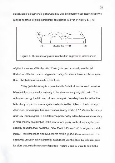
illustration of a segment of polycrystalline thin film interconnect that includes the
explicit portrayal of grains and grain boundaries is given in Figure 8. The
(— ) electron flow (+ )
Figure 8. Illustration of grains in a thin film segment of interconnect.
segment contains several grains. Each grain can be seen to run the full
thickness of the film, which is typical in reality, because interconnects are quite
thin. The thickness is usually 0.5 to 1 |j,m.
Every grain boundary is a potential site for hillock and/or void formation
because it produces a discontinuity in the atom/vacancy migration rate. The
activation energy for diffusion is lower on a grain boundary than it is within the
bulk of a grain, so the atom migration rate should be higher on the boundary.
Aluminum, for example, has an activation energy of about 0.5 eV on a boundary
and 1 eV inside a grain. This difference presumably arises because a boundary
is more loosely packed than is the interior of a grain, so its atoms may be less
strongly bound to their positions. Also, there is more space for migration to take
place. The extra space acts as a source for the generation of vacancies. The
interfaces between grains and their boundaries will therefore be potential sites
for atom accumulation or atom depletion. Figure 9 can be used to see that a

30
grain/grain boundary discontinuity is equivalent to the contact/interconnect
discontinuity discussed previously. The upper part of the figure shows an
interconnect with two end boundaries that can be taken to be contacts of some
kind, and below that is a magnified view of a small region of the interconnect that
includes part of grain 1 ,part of grain 2, and the boundary between them. Since
electromigration occurs more readily in the grain boundary than it does in grain 1
and grain 2, a migration rate divergence is expected. It can be reasoned that
grain 1, the grain boundary, and grain 2 are analogous to the negative contact,
the interconnect, and the positive contact, respectively. Figure 9(b) depicts the
material depletion that might result. The figure does not necessarily give an
contact interconnect contact
grain 1/ grain2\(-)
m
(— ) grain 1 grain2(+)
boundary
Before Electromigration
(a)
contact interconnect contact
-> (-) grainlM grain2(+)
I
boundary
After Electromigration
(b)
Figure 9. Comparison of a grain/grain boundary interface to a
contact/interconnect interface.
(a) Structural equivalence - before electromigration.
(b) Similarity of damage features - after electromigration.

31
accurate portrayal of the relative amounts of depletion (or the absolute amounts,
either). It only illustrates the equivalence of the structural discontinuities and the
similar damage behavior that might be expected.
It would appear then, simply because a grain boundary is so small, that
less depletion is possible there than is possible in the bulk of the interconnect.
The effect of grain boundaries would seem to be relatively insignificant. This
might be true if the electron wind force were exerted only in the direction parallel
to the length of the interconnect, which has apparently been the assumption so
far. It is true that the drift current is directed parallel to the length of the
interconnect, and the electron wind force will certainly be maximum in this
direction. Also, the relatively isotropic nature of a grain renders no need to
consider any other direction. A grain boundary is different. It is relatively
anisotropic, so it would be natural to consider the component of the electron
wind force resolved in its plane. This is especially true in light of the lower
activation energy that is associated with a grain boundary. If the plane of a
boundary is seen as a directed pathway for atom migration, then the lower
activation energy and the vacancy-generating nature of boundaries may more
than negate the apparent insignificance of the boundary size. The extent to
which this is true depends on just how much lower the activation energy is and
on the magnitude of the appropriately resolved component of the electron wind
force. The effective wind force along a grain boundary depends on the angle at
which the boundary is inclined to the downwind direction. The activation energy
for migration on the grain boundary depends on chemical composition and the

32
degree of lattice misorientation between the grains that the boundary separates.
Figure 10 illustrates the way that the electron wind force can be projected onto a
grain boundary to determine the effective force along it. If the length of the
vector Fp represents the magnitude of the wind force parallel to the interconnect
length, then the vector F r represents the force that is directed along a grain
Figure 10. Effective electron wind force, Fr ,
along a grain boundary.
boundary inclined at an angle, a, and
The force F r is the effective driving force for electromigration along the
boundary. Figure 1 1 illustrates what is meant by the "degree of misorientation"
between grains. The figure depicts a two-dimensional arrangement of atoms for
F r= F p cos(cc)
.
(3)
Figure 11. Grains, grain boundary, and misorientation angle, 9.

33
which there appears to be two distinct grain-like domains whose rows are
misaligned by an angle of 9 degrees. The angle, 9, is the misorientation angle
for this two-dimensional case. The transitional region between the ordered
domains illustrates the nature of a grain boundary. It is less ordered and has
extra space. The degree of order and the amount of extra space depend,
somewhat, on the angle, 9. It follows, then, that the activation energy for
migration on this boundary also depends on the value of 9.
Since diffusion, as we have said, occurs more readily on grain boundaries
than it does within the bulk of a grain, and since some component of the electron
wind force acts down the plane of any grain boundary whose angle of inclination
is not 90 degrees, most electromigration damage is, in fact, associated with
grain boundaries. Exceptions to this generality may arise when an interconnect
has very few grains, especially when the associated grain boundaries lay
perpendicular to the length of the interconnect, and when the upwind terminal of
the interconnect is highly resistant to electromigration. In such cases, damage
may occur primarily at the upwind terminal/interconnect interface, similar to that
portrayed in Figure 6, or it may occur at the top and bottom surfaces or the
edges of the interconnect, where the activation energy for diffusion is also
relatively low compared to that for the bulk.
Grain boundary-related damage is frequently associated with so-called
"triple junctions." Figure 12 provides a view of this. The symbols Ji, J2 , and J3
are the atom flux rates that the electron wind force induces on the respectively
indicated grain boundaries. If Ji is smaller than the sum of J2 and J3 , then

34
(-) (+) (-) (+)
Figure 12. Electromig ration at a grain boundary triple junction.
(a) At time zero - Ji < J 2 + J3-
(b) After some time, a void opens up at the triple junction.
material is depleted at the junction of the three boundaries. A void will open.
This is a common way for electromigration damage to show itself when an
interconnect is small-grained and thus has many grain boundaries.
The preceding discussions have dealt with the founding principles of
electromigration - why it occurs and how it exhibits itself. The groundwork laid
by past researchers in this field has been directed toward these two questions.
To reveal why it occurs, theorists have developed descriptions of the electron
wind driving force. To determine how it exhibits itself, work has been devoted to
experimental studies that reveal the importance of certain variables on atomic
migration rate, damage rate, and damage morphology.
There have been several review articles written over the years [1-7].
Some early works are devoted heavily to theory, especially with regard to the
nature of the electromigration driving force [1-3]. In more recent works, attention
is paid primarily, but not entirely, to experimental findings [4-7].
Groundwork and Prior Research

The pure nature of the electromigration driving force can never be truly
determined. But, knowing something of electrical conduction and the actions of
charged particles in an electric field, a reasonable description of the force can
be formulated. A simple treatment in this regard [1] begins by asserting that a
metal is a lattice of positively charged ions that is host to a "gas" of negatively
charged, freely roaming electrons. On average, there is no net charge on a
piece of metal, so the total negative charge associated with the electrons is
equal to the total positive charge of the ions. If an electric field is applied to
such a system of charged particles, represented by a piece of pure, unalloyed
metal, the resultant force, F, on that system can be expressed as
F = njeZjE - neeE , (4)
where
nj is the number density of ions on the lattice,
e is the unit electronic charge,
Zj is the valence of an ion,
E is the magnitude of the electric field,
ne is the number density of free electrons.
The electric field should exert a force on the ions, expressed by the first term of
Equation (4), and on the electrons, expressed by the second term. The resulting
steady state drift of free electrons - the electric current -- is moderated by a
resistance, or friction-like drag force, associated with the interfering ion matrix.
The drag force, Fdrag , associated with the average ion can be expressed as
Fdrag = 8 • E, (5)
where 5 is a coefficient of friction, and the drag force is assumed to be
proportional to the electric field, E. If the drag arises solely as a reaction force

36
associated with the collisions of drifting electrons with the ion matrix, then it is
equal to the force exerted on the ion matrix by the electrons. At steady state, the
total drag force is equal to the total force exerted on the conduction electrons by
the electric field, so it can be resolved that
The summation is included in Equation (6) in appreciation for the fact that every
ion does not contribute equally, at any moment, to the frictional drag. It may be
expected that an activated ion presents a different interference cross section to
a conduction electron than does a normally positioned ion. So, at any moment,
a migrating ion likely makes a different, perhaps larger, contribution to the drag.
The electron wind driving force is associated strictly with the activated ion, so it
should be the center of attention with regard to electromig ration. This being the
case, a different symbol, 8d , will be designated as the friction coefficient to be
associated strictly with migrating ions.
The net force on a migrating ion, Fi , is the sum of the electric field force
and the drag force, that is,
In addition to Fj , this equation contains two quantities which are not known - the
valence of the ion, Zj , and the friction coefficient, 8d . Since an experiment could
be conceived in which the electromigration-related ion velocity is measured, it
neeE = £sk E = nj8E.k=1
(6)
(7)
37
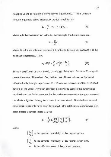
would be useful to relate the ion velocity to Equation (7). This is possible
through a quantity called mobility, Bi , which is defined as
d _ vi
B|"F
(8)
where Vi is the measured ion velocity. According to the Einstein relation,
Di(9)
where Dj is the ion diffusion coefficient, k is the Boltzmann constant and T is the
absolute temperature. Now,
Vi=Bfi = ^e 7\T e;
(10)
Since Vi and Di can be determined, knowledge of the value for either Z\ or 5d will
reveal the value of the other. But, neither one of these values can be found
independently through experiment, so a theoretical estimate must be developed
for one or the other. Any such estimate is unlikely to capture the true physics
involved, and this belief accounts for the earlier statement that the pure nature of
the electromigration driving force cannot be determined. Nonetheless, several
theoretical treatments have been developed. One relatively straightforward and
often-quoted estimate [8] for 8d gives
5h = 4eZ Pd
vNd y v pj y
m(11)
where
Pd
vNd yis the specific "resistivity" of the migrating ions,
is the specific "resistivity" of the normal lattice ions,
m* is the effective mass of the current carriers.

38
Equation (11) implies that the magnitude of the electron wind force, 8dE,
can be represented as a multiple of the electrostatic force, eEZi , where the
factor of multiplication includes the ratio of the "resistivity" contributed by the
migrating ions to the "resistivity" contributed by normally positioned ions. The
term "resistivity" is given in quotes because, in true terms, resistivity is a concept
developed for crystals, not individual atoms. The ratio |m* l/m* is included so that
the direction of the force will be correctly indicated whether the current carriers
happen to be electrons or holes.
i
For convenience, the quantity Zj -—J
is assigned its own name. This
name is "effective valence," and it is given the symbol Z . The value of Z* can be
determined by experiment and the use of Equation (10). Since Z(is part of the
electric field force term and 8d/e is part of the electron wind force (drag force)
term in Equation (7), the sign of Z* indicates which component is larger. If Z* is
positive, then the electric field force is larger than the electron wind force. Ions
will migrate toward the negative terminal. If Z* is negative, then the electron
wind force dominates. Ions will migrate toward the positive terminal. Usually, Z*
is negative. For good metallic conductors, such as the aluminum interconnects
that are the subject here, Z* is negative, and its magnitude is greater than 10.
As such, the electrostatic force is considered a negligible component of the total
electromigration driving force. Electron shielding is probably the cause of its
weak role. This is the reason that the introductory discussion leading up to
Equation (2) conveniently made no mention of the electrostatic force.

39
Another way of presenting the electromigration-induced ion velocity starts
by inserting Z* back into Equation (10). The result is
^4eEZ"4 F- <12 >
The diffusion coefficient, Di , can be expressed as
Dj=D0 exp[—J, (13)
where D0 is a constant and Q is the self-diffusion activation energy. Putting this
into Equation (12) yields
Vi4D° exp(kf)-(14)
In practice, it is customary to express a migration rate as a flux rather than a
velocity, where flux is defined as the quantity of material that passes a plane of
unit cross section per unit time. The ion flux, ^ , is then
where N(is the number of ions per unit volume. Equation (1 5) is a form of the
Nernst-Einstein equation. Equations (12) and (14) are equivalent expressions,
as well. Whatever the form, this relationship is presented in almost any
introductory description of electromigration.
Equation (15) is reminiscent of the relation expressed by Equation (2).
This can be revealed by substituting Fi = eEZ* back into Equation (15) and
replacing E with pj, where p is the resistivity of the conductor and j is the current
density. The result is

40
4»i=
NjepjZ
kT—kT,
' (16)
The ratio of the resistivity to the absolute temperature, ^ , is approximately
constant for a given piece of material over normal temperature ranges. If it is
NeZDreasonable to take — ^ as a constant also, then the two can be combined
k
into one constant called A. Then, Equation (16) becomes
which is effectively the same as Equation (2). The relationship of Equation (17)
was shown, early on, to be quite valid [8]. This suggests that the consolidation
of quantities that led to the constant, A, was not unreasonable.
The primary detriment that electromigration poses to IC interconnects is
the formation of voids or some other type of material depletion. So, ion flux is
not itself the quantity of most concern. This has been discussed in some detail.
Most measurements of electromigration, in engineering practice, are aimed at
damage rate, not ion flux rate. The two should be related, but they are not one
and the same. A standard engineering test for electromigration is the lifetime
test. This is an accelerated test in which a group of test structures is powered
until all of the specimens "fail," where "failure" is identified as a complete loss of
conduction, or, short of such complete failure, some critical increase in electrical
resistance. The distribution of times to failure for the group is examined and the
estimated median of these times is the measure of interest. The median time to
41
failure becomes, then, the measure by which the electromigration reliability of a
particular metallization scheme is compared to another for a given set of test
conditions, or, conversely, the dependence of electromigration reliability on test
conditions is determined for a given metallization scheme. The test conditions of
interest are current density and temperature. The important characteristics of a
given metallization scheme are chemical composition, microstructure, and
macrostructure. These factors were stressed on page 6 in the INTRODUCTION.
It is reasonable to guess that the median time to failure is inversely
related to the rate of damage inflicted by the electron wind. Although ion flux
rate and damage rate are not one and the same, a commonly used model for the
median time to failure, tso , is
which, except for the exponent n, is effectively the reciprocal of Equation (17).
Equation (18) is a generalized form of what has become known as "Black's
Equation." Black popularized the use of such a model in electromigration work,
and he supported a value of n = 2 in an early paper [9].
Equation (18) includes j and T in explicit form. The other major factors -
chemical composition, microstructure, and macrostructure - are implicit in the
quantities A and Q. The activation energy, Q, is of particular interest, because,
being in the exponential, it exerts a heavy influence on tso. The following review
will address each of the primary factors in turn.
(18)
42
Current Density
The exponent, n, of Equation (18), is usually the center of discussion
regarding the role of current density. An early study on bulk metals suggested
that a value of n = 1 is quite appropriate [8], and most have agreed that this is
the correct theoretical value. Studies on thin films, however, have not yielded a
consistent result. Early experimental work [9-12] revealed values of n between
2 and 3, and a value of 1 .5 was found in a later attempt to clarify the matter [13].
Theoretical arguments have given support to n=1 [14,15] and n=2 [9,16,17]. The
dependence of energy dissipation on f is one possible basis for believing n=2,
but the energy that is actually dissipated per electron/ion interaction is negligible
compared to the activation energy. The electric current, in its role as a driving
force for migration, should be viewed only as a biasing influence on the basic
diffusion process. In this view, such bias should be proportional to j. Support for
n=1 is generally accompanied by arguments that an apparent value of n larger
than 1 arises when the temperature is not accurately characterized throughout
the test. This is believable, because it is practically impossible to follow the
temperature throughout the entire failure process. As electromigration damage
proceeds, the current density and temperature increase at the damage site.
Such a phenomenon is difficult to account for experimentally. When a test is run
with the smallest practical initial current density and the test structure makes use
of good thermal management, n is probably between 1 and 2. It is very common
to see the use of n=2.
43
Temperature
There is apparently no questioning the placement of T in an exponential
term, as presented in Equation (18). This so-called Arrhenius dependence is
well entrenched as a part of all models that incorporate thermal activation. The
variable, T, is sometimes placed as a pre-exponential component, as well. This
is apparently done in appreciation for the fact that it may not be strictly correct to
consider the pre-exponential quantity of Equation (16), especially the factor Z,
to be independent of temperature [4]. So, a slightly modified expression for tso
may appear as
t50 =^expf£l. (19)j" "VkT
And, an equation of the form
AT3 f Q\tso=— exp £1 (20)
has been offered as an appropriate option when temperature gradients
contribute heavily to the driving force for damage [18]. In any case, the
dominance of the exponential factor makes the choice of including or excluding
the extra T factor in Equations (19) and (20) somewhat moot in light of normal
experimental error. Equation (18) is usually acceptable.
Chemical Composition
Such physical properties as atomic mass and inter-atom bond strength,
which vary with chemical identity, determine how well any atom in a given piece
of material resists a diffusive hop from its position. This barrier is essentially a

44
measure of the activation energy, Q. So, chemical composition affects tso largely
through Q. It also has a strong role in determining A, but again, the exponential
factor exerts a dominant influence.
Much of the early work on electromigration was directed at determining Q
for various metals and alloys. Heavy attention was placed on gold [8,12,19-22],
silver [19], copper [23], and especially aluminum [10,24-29]. Determination of Q
usually involves the measurement of tso or ion velocity for several different test
temperatures with other conditions held constant. An Arrhenius plot is made,
that is, Iog(t5o), log(Vj) or log(Vj/j) is plotted versus 1/T, and Q is extracted from
the slope of the resulting straight line fit.
The activation energy that is commonly observed for pure aluminum is
about 0.5 eV [10,24,25]. For gold, it is about 0.9 eV [19-22], and for copper it is
about 0.8 eV [23]. The importance of knowing these values lies in the huge
effect that they have on tso. At a temperature of 350 K, the value of exp(Q/kT) for
aluminum (Q = 0.5 eV) is 1.6x10⁷
. The value of exp(Q/kT) for gold (Q = 0.9 eV)
is 9.7x1
0
12at the same temperature. The choice of material is certainly a pivotal
issue, but before making any conclusions, it is important to note that the Q
values quoted here happen to be those for migration on grain boundaries. This
detail will be addressed in the next section.
Microstructure
The chemical identity of a conductor is not all that determines Q. Just as
important is its microstructure, because atomic migration may proceed not only
through the bulk, but it may also follow an easier course on free surfaces, grain

45
boundaries and other types of interfaces, the presence of which help to define
the "microstructure" of a given piece of material. The values of Q quoted in the
last section were found under conditions for which grain boundary migration was
dominant. This is a critical detail. Using aluminum as an example, and staying
with T = 350 K, the activation energy for lattice migration (which is about 1.1 eV)
leads to a value for exp(Q/kT) of 7.4x1
0
15, which is far different from the value of
1 .6x107that was obtained above for migration on grain boundaries. The value
of Q on grain boundaries is smaller than it is on the lattice presumably because
atoms are less densely packed on grain boundaries and less strongly bound. A
similar reasoning leads to the conclusion that Q on free surfaces is even smaller
than it is on grain boundaries.
The apparent activation energy will depend on the temperature and the
availability of the various types of migration pathways. At high temperatures,
perhaps 350 °C and above, lattice migration occurs readily, and the apparent
activation energy will be that for bulk migration. At intermediate temperatures,
perhaps 150 °C to 350 °C, the lattice may not contribute much as a pathway.
The apparent activation energy will likely be that for grain boundary migration if
grain boundaries are available in sufficient quantity. At lower temperatures, it
might be that even grain boundaries do not provide a good means of migration.
In these cases the apparent activation energy may be that for migration on a free
surface if one or more is available. The transitions between these cases need
not be abrupt, that is, a mixture of diffusion modes may be apparent whenever
the temperature and the availability of a particular pathway are marginal. For

example, in an experiment on aluminum [24] it was found that films with a small
grain size displayed a Q of 0.51 eV, whereas films with a larger grain size
displayed a Q of 0.73 eV. The films with small grains presumably contained a
plentiful supply of grain boundaries and therefore showed an activation energy
that is accepted to be that for grain boundary migration. The large-grained films
had fewer grain boundaries, perhaps a marginal quantity, such that a relevant
fraction of the damage occurred by lattice migration. So, in the temperature
range used for that particular test, the large-grained films appeared to have an
activation energy between that for grain boundary migration (-0.5 eV) and lattice
migration (-1.1 eV).
The traditionally heavy attention paid to grain boundaries as pathways for
electromigration is fueled by the reality that, until recently, any particular IC
interconnection was likely to have a plentiful supply of them. The tendency for
damage to occur along grain boundaries was observed in situ during an early
TEM experiment [27]. Observations were made on large-grained samples and
small-grained samples of Al. It was particularly revealing that the voids which
formed on the small-grained samples were irregular in shape, whereas those
formed on the large-grained samples consistently had straight edges. This was
taken as evidence that voids propagate on the boundaries rather than through
the grains.
Evidence that grain boundary triple junctions provide natural sites for the
formation of voids was also obtained early on in another in situ TEM study [28].
This study, performed on Al, showed not only that voids form preferentially at
47
triple junctions, but also showed that the propagation of a given void will proceed
down the outgoing grain boundary that is most favorably oriented relative to the
electron wind. That is, the boundary with the largest resolved force component
becomes the preferred pathway for propagation beyond the triple junction. See
Figure 10 in this regard. A grain boundary triple junction is a natural site for void
formation when two of its three associated grain boundaries are arranged as
outgoing pathways and the other is arranged as an incoming pathway. In such a
configuration, the outgoing grain boundaries, in combination, will likely (but not
necessarily) carry material away from the junction at a faster rate than material
can be brought in by the single incoming grain boundary. This scenario was
illustrated in Figure 12. Of course, the converse arrangement of boundaries
should encourage hillock formation at the junction.
Certainly, the number of grain boundaries that will be found in a given
width of interconnect is inversely related to the average size of its grains, so it is
not surprising to find consistent results in studies of tso versus grain size. The
median time to failure invariably increases as grain size is increased. Some
have reported this dependence to be nearly linear [30-33]. The observation that
an increase in grain size may be accompanied by an apparent increase in
activation energy [10,24,34] suggests that a reduction in the number of grain
boundaries available for migration sometimes allows lattice migration to play a
noticeable role.
The effect of the grain size distribution on tso is based on a principle
similar to that applied in explaining why triple junctions are prone to damage.

48
With a mixture of grain sizes, there are bound to be some regions in which the
number of grain boundaries is different from the number in adjoining regions.
The transitional zone between each region is equivalent, on a larger scale, to a
grain boundary triple junction, and damage may occur preferentially in such a
zone. Such a structural gradient represents a vulnerability beyond that which is
already contributed by the triple junctions themselves. So, tso should decrease
as the standard deviation of the grain size is increased. Experiments have
confirmed that it does [35]. A large standard deviation in the grain size may,
itself, magnify the vulnerability to void formation, even if there is no bias in the
location of any given grain according to its size. It could happen, however, that
there is such a bias. For example, if the larger grains are all located more
toward the upwind end, and the smaller grains are all located more toward the
downwind end of the interconnect, then void formation should be encouraged
most strongly where the transition in grain size is the sharpest. Again, such
behavior has been verified by experiment [24,36].
It was mentioned, in connection with the two-dimensional illustration of
Figure 1 1 , that the activation energy for migration on a grain boundary is related
to the angle of misorientation between the grains that it separates. A universally
applicable characterization of such a dependence in three dimensions is difficult.
At least one effect associated with crystallographic orientation has been clearly
demonstrated, though. Thin films with a large degree of {1 1 1} fiber texture have
been shown to exhibit larger median times to failure [24,34,37-42]. Presumably,
when the {111} plane of all grains is aligned parallel to the substrate surface, the

resulting grain boundaries are largely tilt boundaries. Cohesion may be stronger
on these boundaries than it is on randomly obtained boundaries. The superior
mechanical strength displayed by the {111} plane relative to other planes [43]
lends support to this view. In addition, tilt boundaries are composed of steps
and ledges, where the steps are essentially dislocations whose lengths are
aligned normal to the film plane. With this alignment, the steps might act as
blockades against in-plane migration [37]. It seems, then, that the activation
energy on such grain boundaries should be larger than it is for boundaries
between randomly oriented grains.
An empirical relationship has been proposed for the dependence of tso on
the microstructural characteristics just discussed - grain size, grain size
distribution, and {111} texture [42]. It is given as
*50 *a2
1(111)
^'(200);
(21)
where
S is the median grain size,
a is the standard deviation of the grain size distribution,
'(111)
0(200);
is a measure of the {111} texture based on x-ray intensities.
The ratio of x-ray intensities, l(m/l(2oo) , is obtained from an x-ray diffractometer
measurement. According to the JCPDS files for Al, this ratio is about 2 for a
powder sample, which is assumed to have randomly oriented grains. If the ratio
measured for a thin film is much larger than 2, then, it is considered to display a
{111} texture. Films deposited by some techniques, particularly ion-assisted
techniques, can be so highly textured that l (2oo) is almost unmeasurable [34].
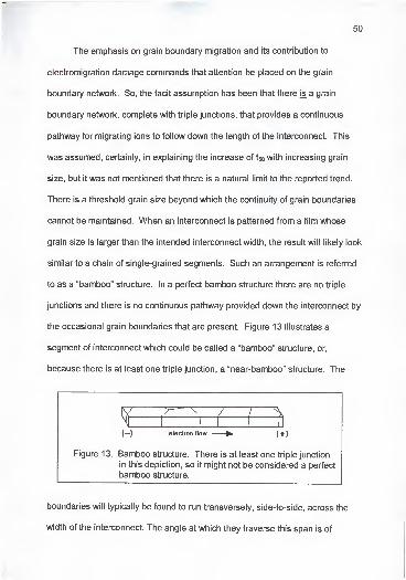
50
The emphasis on grain boundary migration and its contribution to
electromigration damage commands that attention be placed on the grain
boundary network. So, the tacit assumption has been that there is a grain
boundary network, complete with triple junctions, that provides a continuous
pathway for migrating ions to follow down the length of the interconnect. This
was assumed, certainly, in explaining the increase of t5o with increasing grain
size, but it was not mentioned that there is a natural limit to the reported trend.
There is a threshold grain size beyond which the continuity of grain boundaries
cannot be maintained. When an interconnect is patterned from a film whose
grain size is larger than the intended interconnect width, the result will likely look
similar to a chain of single-grained segments. Such an arrangement is referred
to as a "bamboo" structure. In a perfect bamboo structure there are no triple
junctions and there is no continuous pathway provided down the interconnect by
the occasional grain boundaries that are present. Figure 13 illustrates a
segment of interconnect which could be called a "bamboo" structure, or,
because there is at least one triple junction, a "near-bamboo" structure. The
(+)
Figure 13. Bamboo structure. There is at least one triple junction
in this depiction, so it might not be considered a perfect
bamboo structure.
boundaries will typically be found to run transversely, side-to-side, across the
width of the interconnect. The angle at which they traverse this span is of

51
importance. If the traversing boundary is inclined at any angle other than 90
degrees with respect to the downwind direction, then there will likely be some
migration on that boundary. A void may form on the edge of the interconnect at
the upwind end of that grain boundary segment. The tendency for this to
happen will be greater the smaller the inclination angle and the longer the
traversing grain boundary, because the resolved component of the electron wind
force is larger with decreasing angle and there is more downwind room, that is, a
larger sink, for migrating atoms on longer segments. In any case, the absence
or near absence of triple junctions and the lack of a continuous network of
pathways should lead to larger tso values for interconnections with bamboo and
near-bamboo grain structures. It might also be estimated that the location and
mode of failure is more unpredictable with these structures, and especially with
near-bamboo structures, because those interconnects that just happen to
contain a triple junction might fail long before those that do not. Concern for this
complication was expressed quite early on [44], but the predicted increase in tso
has indeed been confirmed by experiment [45,46].
The idea of reducing the number of grain boundaries can certainly be
taken to the extreme case by considering their total elimination. Single crystal
interconnects should be the most reliable of all. Indeed, they were observed to
be nearly immune to electromigration damage [47], but the production of single
crystal interconnects as routine procedure has not been possible. It is routinely
possible to obtain bamboo structures, however.

52
Another structure absent of grain boundaries is the amorphous structure.
Prompted by the knowledge that amorphous alloys often make good diffusion
barriers, an experimental comparison of electromigration lifetime was made
between films composed of an amorphous Cu-Ti alloy and crystallized films of
the same composition [48]. The amorphous films showed about a ten-fold
improvement in lifetime. There was no comment made on the resistivity of the
amorphous films compared to that of the crystalline films.
In unalloyed metals, grains and grain boundaries are certainly the most
significant microstructural features with regard to electromigration. This can
probably be said for alloys as well, but the addition of alloying elements does
bring on an additional set of considerations. These considerations consist, at
least, of the migration behavior of the solute, the effect of the solute on the
migration behavior of the solvent, and the effect of any additional phases that
precipitate out.
Aluminum has enjoyed the most attention as a base metal in the study of
alloying effects, since it is the predominant interconnect material. The most
heavily considered alloying additions have probably been silicon and copper.
Both improve the electromigration resistance of aluminum [11,49-51], but copper
is especially effective and has made the biggest impact. The addition of copper
has proved to be one of the most significant defenses against electromigration.
The mechanism by which copper additions improve the reliability of Al
interconnections was vigorously debated and studied early on. New doubts are
raised on occasion, but an integral part of most explanations is related to the

precipitation of CuAI2 on grain boundaries. Copper moves quite well on Al grain
boundaries, but the self-diffusion of Al on those same boundaries seems to be
inhibited by the presence of the Cu [1 1 ,37,52-54]. If the copper is eventually
depleted, void formation follows quickly, but such depletion is prevented or
significantly slowed so long as CuAI2 particles are present. Presumably, the
precipitates are a replenishing source of Cu atoms.
The measured activation energy for the failure of AI(Cu) thin films is
sometimes as high as 0.8 eV [55]. Since failure seems to depend on the
depletion of Cu atoms from Al grain boundaries, the activation energy should be
associated not only with the diffusion of Cu on those boundaries, but also with
the mechanism by which the boundaries are replenished with Cu atoms in the
presence of CuAI2 . Such quantities as the heat of solution of Cu atoms in Al and
the heat of adsorption of Cu atoms on Al grain boundaries should play a role in
determining the overall activation energy [55].
Of course, copper and silicon are not the only alloying additions that have
been considered. Gold, silver, magnesium, and nickel (to name a few) have
also been investigated. Magnesium [56] and nickel [57] are beneficial additions.
Gold and silver are not [1 1].
Macrostructure
The term "macrostructure," as it is meant here, may encompass just about
any defining characteristic of an interconnection that is not an inherent part of
the microscopic world. It includes size, shape, and other macroscopic features
of construction.

54
Although macrostructure is a property that is inherently independent of
microstructure, the reverse is not strictly true. For example, the grain boundary
network that happens to be captured when an interconnect is patterned from a
thin film depends on the length and width of the pattern taken. A larger number
of unfavorable structural features, such as triple junctions, is captured along the
length of a patterned interconnect as that length is increased. Also, the chance
that such unfavorable sites will turn up in the "upwind portion" of the interconnect
is better with increasing line length. It is not very surprising, then, that tso has
been found to decrease with increasing interconnect line length [58-60].
A similar reasoning can be applied when considering the interconnect
width. With increasing width, the probability of capturing damage prone
structural features should increase. With this reasoning alone, it appears that tso
should decrease with increasing linewidth. It is important to realize, however,
that the length of an interconnect is usually much greater than the width, so void
propagation across the width is usually the ultimate cause of failure. As the
width is increased, then, a given void must expand farther to cause failure. Also,
with linewidths that are large enough to capture several triple junctions, it is less
likely with increasing linewidth that all of the triple junctions in a randomly
chosen side-to-side span will void and link together. Apparently, then, it may
also be reasoned that tso should increase as linewidth is increased. The two
lines of reasoning are in contradiction, but experimentation has shown the
second approach to be more appropriate. That is, tso increases with increasing
55
linewidth [58]. An empirical relationship was constructed for tso versus line
length and linewidth [58]. It was reported as
t5o=A-w-exp^-J , (22)
where
A is a constant,
w is the linewidth,
a is a constant that depends on w,
t is the line length.
This equation indicates that tso increases linearly with linewidth. The
dependence on length is one in which tso first decreases rather quickly with
increasing line length, but eventually appears to level out as the rate of
decrease becomes negligibly small.
It should be noted that the smallest linewidth tested in the experimental
determination of Equation (22) was 5 ^m, and the grain size was reported to be
equal to or less than 2 urn. Equation (22) indicates that tso decreases linearly as
linewidth is decreased, but, if a linewidth of, say 1 ^m, had been tested, it is
likely that the tso for that line would have been larger than the tso for the 5 urn
line. This is because a 1 line would likely have a bamboo structure. This
effect was mentioned earlier in the context of increasing grain size. There are
two ways, then, to arrive at a bamboo structure. One way is to increase the
grain size until the average grain is larger than the interconnect is wide. The
other way is to reduce the linewidth until it is smaller than the size of the average
grain. Now, an increase in tso was reported [45,46] in the context of increasing
grain size, so a similar increase is reported [61-65] in the context of decreasing

56
linewidth. The critical width below which tso increases depends, of course, on
the grain size of the film from which the interconnect is patterned. The critical
width appears to be 1-2 urn in practice.
In addition to size, the macrostructure of an interconnect is defined by its
terminations and the other purposeful or incidental types of contact that it makes
with other materials on the chip. Certainly, an interconnection must lay on top of
another material, and it is also routine that other materials are placed over it.
For example, it is standard practice to "passivate" IC chips, that is, encapsulate
them with a protective coating. If any particular passivation coating might
improve electromigration lifetime, all the better. Of course, this is mentioned
because some coatings do seem to be beneficial.
Early reports on the effect of coatings claimed that the activation energy
of 0.84 eV for large-grained, uncoated Al films was increased to 1 .2 eV when the
films were coated with Si02 glass [9,10]. Another study showed an improvement
in lifetime for aluminum films that were coated with an alumina-silicate glass [26].
The explanation by the authors in both cases was that surface diffusion was
inhibited by the coatings. This explanation was challenged [66] by pointing to a
study [47] that had shown films of uncoated, single-crystal Al to be essentially
immune to electromigration. In addition, it was noted that the native oxide that
forms on the surface of Al should inhibit surface migration just as well as any
additional coating would, anyway. An alternative proposal was that coatings
might be capable of suppressing the formation of hillocks, which in turn, it was
thought, should prevent the formation of voids. Calculations of the strengths of

57
coatings and the forces that might be produced by electromigration led to the
conclusion that coatings would have to be very strong to be effective, possibly
stronger than can practically be obtained [66]. It was suggested that the
proposed mechanism could be effective only for very thin films and relatively
thick coatings.
Later work, in which aluminum films were coated with silicon nitride,
indicated again that the coating slows the drift of atoms [67]. It was commented,
in addition, that the strength of a coating does not have to be so high as was
calculated in the earlier work. This statement was based on the notion that
electromigration-induced compressive stresses are built up locally across each
point of atom depletion and its associated point of accumulation just downwind,
and this source-sink distance is often quite small compared to the total length of
long conductors. Back-diffusion is encouraged by the local stress gradient
between the source and sink.
Overcoatings of doped glass and/or silicon nitride are, in fact, commonly
used in the construction of an IC. Also, being that IC circuitry is built up in a
multilayered arrangement, dielectric materials are necessary between each
layer. These may be composed of Si02 , as well.
In addition to passivations and dielectrics, it is also fairly routine to find
the use of interconnect cladding layers, which are used for various purposes,
such as the prevention of interdiffusion or the promotion of adhesion between
layers. Materials commonly found in these roles are Ti, TiN, W, and TiW. Such
claddings are usually significantly thinner than the interconnect itself, so any

58
influence that they exert on electromigration behavior is associated with
interdiffusion or crystallographic effects on the deposition of the aluminum film.
Finally, any segment of interconnect must eventually make contact to a
silicon device or an interlevel splice of some kind. Being that the sole purpose
of an interconnection is to make connections between silicon-based devices on
a chip, the Al/Si contact interface has a long research history. The reliability
concerns associated with this interface are largely related to its metallurgy and
the interdiffusion of Si and Al. With respect to electromigration specifically, a
silicon device can essentially be disassembled one atom at a time by an electron
wind. Even when barrier materials are successfully introduced to avoid the loss
of silicon and the invasion of aluminum, the macrostructural discontinuity that
must inherently be associated with the interface is sure to be a favorable site for
aluminum depletion when the interconnect carries a sufficiently large current.
Such a scenario was discussed in connection with Figures 5 and 6.
Another type of contact concern is a more recent arrival. The multilevel
arrangement of today's IC designs requires a means of connecting the circuitry
on any given level to that on other levels. Such connections are made through
small openings etched through the dielectric that separates the layers. An
illustration of such a contact arrangement is given in Figure 14. The figure
depicts a portion of two metallization layers. The two segments of aluminum
interconnect, one on the lower layer and the other on the next layer up, are
connected by way of a small segment of tungsten. The surrounding matrix area
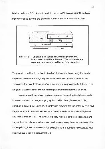
59
is taken to be an Si02 dielectric, and the so-called "tungsten plug" fills a hole
that was etched through the dielectric during a previous processing step.
;"A1
J
sio2
1 M
w Si02
\ Al e= * Al\
Figure 14. "Tungsten plug" splice between segments of Al
interconnect on different levels. The two levels are
separated and surrounded by an Si02 dielectric.
Tungsten is used for this splice instead of aluminum because tungsten can be
deposited into very narrow, deep via holes more readily than aluminum can.
This opens the door for the use of very narrow interconnections (< 0.3 |j.m). The
tungsten process also allows for a more planarized arrangement of levels.
Again, as with the silicon contact, a severe macrostructural discontinuity
is associated with the tungsten plug splice. With a flow of electrons in the
direction indicated by Figure 14, the interface between the top of the W plug and
the upper level Al interconnect will be a prime location for aluminum depletion
and void formation [68]. The tungsten is very resistant to the electron wind and
stays intact, but aluminum atoms are readily swept away from the interface. It is
not surprising, then, that electromigration failures are frequently associated with
this interface when it is present [69-73].

Modern Implications
The preceding discussion of fundamentals and founding research is all
pertinent and contributory to the state of the art applications of today. That is,
the description of electromigration and the characterization of its effects are
essentially no different today than they were after the first decade or so of
research. Challenges of recent years are largely associated with the drive for
increased IC packing density, which has led to the use of multilevel structures
and very small interconnect linewidths. The following list summarizes the most
pertinent features of modern IC interconnects:
1. Composition: alloy of aluminum (1- 4% Cu). Claddings may be included.
2. Local operating temperature: may approach 100 °C.
3. Current density: may approach 1x1
0
6A/cm
2.
4. Linewidth: < 1 ^m.
5. Thickness: < 1 (am.
6. Grain structure: near-bamboo or bamboo.
7. Interconnect architecture: multileveled, with W plug interlevel splices.
It might be estimated, in light of previous discussions, that an interconnect
with these specifications is reasonably resistant to electromigration. Although
the tungsten plug is unfavorable, the bamboo or near-bamboo grain structure
and the copper alloying should prevent the electron wind from sweeping copper
and aluminum away from the plug.

61
In reality, a temperature of 100 °C and a current density of 1x10⁶A/cm
2
are quite severe by traditional standards, so the advantage that is gained from
the bamboo or near-bamboo grain structure is minimized. Interestingly, the
reduction in linewidths that brought in the bamboo structure is also the reason
that current densities are increasingly severe. Ultimately, the absence or near
absence of grain boundaries does not preclude the migration of Cu and Al along
other paths. In traditional polycrystalline interconnects, these alternate routes
were relatively insignificant compared to the plentiful supply of grain boundaries
that was typically present, but with increasingly narrow interconnects (0.25 ?)
and more severe current densities, they can no longer be ignored. Recent
studies have revealed, for example, that significant degradation can result from
lattice migration and edge migration, in addition to grain boundary migration
within the polycrystalline segments that sometimes appear alongside the single
crystal segments in near-bamboo interconnects [70-72,74,75].
Black's equation was introduced earlier as the most popular model of
electromigration lifetime. It is repeated now for further consideration.
The current density, j, is apparently taken to be constant during the course of an
experiment, but if a time varying current is employed, some modification should
be made to the equation.
Pulsed Electromigration
(18)

62
Any ordinary current variation could be considered, but, in keeping with
the subject of this work, let us consider a unidirectional pulsed current of the
type that was depicted in Figure 1 . Assume, for the moment, that tso is known for
a group of test stripes that was subjected to a constant current of magnitude A.
If a second group of identical test stripes is subjected to a pulsed current, where
the amplitude is A and the duty cycle is 50%, what is the expected tso for this
group? Of course, the temperature is assumed to be the same for both tests.
As a first estimate, it might be assumed that normal electromigration
occurs for the duration of each pulse and that nothing happens between pulses.
If this is true, tso for the second group is expected to be twice the known tso of the
first group. That is, Black's equation might be modified to read
where d is the duty cycle expressed as a fraction and j is the pulse amplitude.
Another way to state this relationship, if it is correct, is to say that the median
number of on-time hours to failure for the second group is equal to the median
number of hours to failure for the first group. Equation (23) is therefore said to
express an "on-time" dependence.
Another approach may be to consider the existence of an effective dc
current density that might be equivalent to the given pulsed current density. The
first obvious candidate for such a quantity is the average of the pulsed current
density waveform, which is just d j for the square pulses considered. So, if j is
replaced by d •j , then Black's equation would become
(23)
t50 =A
(24)
(dj)'n•exp
KkJJ'
This relation is known as the "average current density" model.
Recall, from earlier discussions, that the "correct" value of n in Black's
equation is not known. Estimates generally fall between 1 and 3, but much
larger values (as high as 15) have been reported. So, it may be useful to
separate the duty cycle dependence from the uncertainty associated with the
value of n. The result might be
Of course, this expression represents an average current density dependence
only when m = n.
A value of m = 1 produces the on-time model. A larger value indicates a
larger tso, and in such a case the lifetime is said to be "enhanced." The average
current density model predicts enhanced lifetimes, because it is defined by m=n,
and n is normally taken to be 2.
Neither the on-time model nor the average current density model makes
explicit mention of the pulse repetition rate (frequency). The assumption that
leads to an on-time model is that "normal" electromigration begins immediately
at the start of a pulse, proceeds in the same way that it would for a constant DC
current of the same magnitude, then ceases immediately at the end of the pulse.
In addition, the time between pulses is treated as though it has no effect on the
process. Such an assumption seems to exclude any consideration of frequency
(25)
64
from the start. However, implicit in the average current density model must be
an assumption that something does happen between pulses or a pulse is not
equivalent to an equal interval of time in a DC experiment or both. This is an
implicit recognition that additional transients might exist, just none that are
altered according to frequency. In the end, the role of frequency is not so easy
to speculate on, but it is quite apparent that duty cycle should affect tso.
No wide range, continuous dependence of tso on pulse frequency has
been identified with any conclusive experimental evidence or by any compelling
theoretical argument. Any observed dependence on frequency has been limited
to a low frequency critical point transition that is apparently associated with the
response times of thermal transients. Except for this, the frequency seems to be
a minor influence compared to duty cycle. Nonetheless, frequency is given
continued consideration, in view of the possibility that another critical point or
perhaps a continuous dependence of some sort exists at high frequencies. In
addition, even the dominant influence of duty cycle has been difficult to
characterize. There is considerable disagreement about how it should be
incorporated into a quantitative model. Although it is common to see use of a
model like Equation (25), the fitted value of m is not consistent.
The first experimental study of electromigration under pulsed current
conditions was carried out by English, Tai, and Turner on Ti-Au thin films [76].
They compared the effects of several different sets of pulse conditions, ranging
in frequency from 1CT4Hz to 10
4Hz, and in duty cycle from 10% to 70%. Each
pulse treatment was applied for 100 on-time hours, that is, the total "exposure"
65
was the same for every test. The post-test condition of the films was observed
by SEM, and it was found that the samples exhibited heavy damage, moderate
damage, or no damage, depending on the pulse frequency and duty cycle that
had been applied.
The authors' explanation began with the common assumption that
electromigration damage is the ultimate result of a local buildup of vacancy
concentration at some point of flux divergence. The buildup was assumed to
take place rapidly at first, but to eventually slow down while approaching some
maximum level of local supersatu ration. Under pulsed powering, it was figured
that this level of supersaturation might be reachable during the time span of a
sufficiently long pulse, but the level was expected to decay somewhat during the
off time between pulses. The idea was then introduced that some critical level of
supersaturation had to be maintained or exceeded for a sufficient length of time,
called the "incubation" time, in order for damage to nucleate in the form of voids.
Unlike the vacancy supersaturation, voids were considered to be stable against
any relaxation effects associated with the time between pulses.
This reasoning appeared to be particularly effective in the analysis of low
frequency behavior, where the pulses were presumed to be long enough that
stable voids may be formed within the duration of one pulse. In such a regime,
the off time between pulses would be of little significance, and the duty cycle
would be unimportant, except to lengthen the total time to failure. An on-time
dependence would then be exhibited. Some critical pulse length should define
the edge of this regime, but its exact value is difficult to predict. It was estimated

66
by Rosenberg and Ohring [77] that the supersaturation rise time is on the order
of 100 seconds in aluminum (T = 125 °C and J = 106A/cm
2), but they did not
offer any estimate of an incubation time.
The analysis was continued by considering the possible response to
pulse lengths that happen to be shorter than the critical time period for void
nucleation, but long enough to produce a large supersaturation of vacancies on
one pulse cycle. It was reasoned that the build up of vacancy supersaturation,
because it would be large enough to produce a considerable driving force for
recovery, could be nearly eliminated during the off time if it was about equal to
the on time. Very long, highly enhanced lifetimes could then be the result. The
actual response in this intermediate regime was expected to be a function of the
pulse duty cycle and frequency.
The likely response to very short on times and off times was said to be
different. For such conditions, each pulse was assumed to produce a relatively
small increase in the vacancy supersaturation, and each following off time was
assumed to allow little recovery. The supersaturation was expected to increase
in small increments with each pulse cycle, to eventually reach the critical level,
and to stay above that level for a sufficient length of time for void nucleation.
According to the authors, the required number of cycles would depend mostly on
the duty cycle and not so much on the frequency. They contended that the rise
and fall of supersaturation could each be adequately approximated as a linear
function of time for arbitrarily small pulse lengths and pulse separations, so the

relative lengths of the on times and off times would determine the behavior, not
the individual times themselves.
The concept of vacancy supersaturation has remained a commonly used
tool in modeling and/or explaining pulsed electromigration behavior. However,
instead of requiring a void incubation period, many treatments just follow the
assumption that the time to failure is inversely proportional to the threshold level
of supersaturation. In any event, the electromigration damage mechanism is
probably more complicated than either approach implies. In addition to excess
vacancies, other types of defects probably form along the way, and these may
have different implications regarding the kinetics of damage formation and the
enhancement of lifetime. In addition, it is known that a downwind compressive
stress may be built up during the course of electromigration [67,78]. When this
is the case, lifetime enhancement should be associated somewhat with stress
driven recovery of damage between pulses. Finally, if it happens that the pulse
length is too short for the temperature of the test stripe to attain its steady state
DC level, then lifetime should be enhanced. In fact, this consideration received
heavy attention in the earliest studies. These issues have been considered in
various forms [15,79-117] since the initial study of English, Tai, and Turner.
The first treatment of temperature and thermal response effects was
offered by Sigsbee [15]. He considered the electromigration-induced growth of a
crack across the width of a test stripe in conjunction with the pulsating Joule
heat dissipated by a pulsed current. He attributed lifetime enhancement to the
lower average temperature that results when the current is pulsed. He noted, in

addition, that there is some minimum frequency (around 1 KHz in his modeled
system) below which the pulse length is long enough that the temperature is
able to reach its steady state DC value for much of the pulse duration and the off
time is long enough for the temperature to return to ambient for much of the time
between pulses. An on-time dependence was then expected.
Davis [79] also presented a thermal treatment, but he contended that the
average temperature is not a useful quantity and that the temperature has to be
followed over the whole course of a pulse cycle. He demonstrated a variation in
the degree of lifetime enhancement with frequency for fixed duty cycle over the
range 4 KHz to 300 KHz, even though the average stripe temperature was the
same in each case.
Miller [80] found that the duty cycle was the primary factor in a range of
frequencies from 20 KHz to 250 KHz. He made a temperature correction to his
data and concluded that lifetime enhancement was caused largely by some type
of damage relaxation process, and not only by thermal enhancement of the type
treated by Sigsbee and Davis. The lifetime with a 50% duty cycle was found to
be 20 times larger than the DC lifetime. Miller's data followed the empirical
relationship
t50 = Bexp(-Md), (26)
where tso was given in on-time hours, B and M were constants, and d was the
duty cycle. He attempted to justify this relationship by invoking the concept of
excess vacancy concentration and by postulating that this concentration rises
during each pulse and falls during each off time between pulses according to an

69
exponential time dependence. Schoen [82] also developed a model that was
based on an exponential decay of damage between pulses, in addition to a
decrease in temperature, and found that Miller's data could be readily explained.
These findings caused excitement in the research community, but such highly
enhanced lifetimes have not been found by others without the presence of
severe thermal effects.
Wu and McNutt [84] confirmed the role of thermal effects in producing
extremely large lifetime enhancements, by extending the work of Miller. Their
analysis was based on a quantity, similar to the vacancy supersaturation, which
they called the "microscopic damage concentration." This quantity was assumed
to attain some asymptotic value, which was said to depend on the pulse duty
cycle and on the temperature-dependent characteristic rise and fall times of the
damage concentration. By requiring that tso be inversely proportional to the
asymptotic damage concentration, the following expression was developed:
where d is the duty cycle and F r was called the "damage relaxation factor." The
damage relaxation factor was defined as
where xd is the damage generation time constant and x r is the damage relaxation
time constant. These expressions were later re-examined by Suehle and Schafft
and were found to be useful in explaining the current density dependences of
pulsed electromigration [97].
(27)
(28)
70
In an attempt to clear up what they perceived as confusion in the research
community over the roles of duty cycle and damage relaxation, English and
Kinsbron [85] carried out a study in which the electromigration ion velocity was
measured as a function of pulse duty cycle and frequency. They sought to avoid
temperature excursions by keeping current densities below 2x10⁶A/cm
2, and
they employed test frequencies from 0.01 Hz to 100 KHz and duty cycles from
1 .5% to 100%. Their test temperature was 362 °C. Oddly enough, their results
indicated that the ion velocity, in terms of on-time, was the same regardless of
frequency and duty cycle. They concluded that there was no damage recovery
associated with the time between pulses.
It was already mentioned that some critical frequency might exist, below
which the behavior observed by English and Kinsbron should occur. That is, an
on-time dependence may be exhibited when the duration of each pulse exceeds
the time necessary to produce unrecoverable damage. The transition frequency
should be well below 100 KHz. An on-time dependence might also be favored
whenever Joule heating is a factor and the pulse width is much larger than the
thermal time constant of the test structure. The transition frequency in this case
could be as high as 100 KHz, but English and Kinsbron conducted their study
with the specific intention of avoiding thermal influences. The implications of
their results are unclear.
The first demonstration of an average current density dependence was
reported by Towner and van de Ven [86], who observed such a relationship at a
frequency of 1 KHz with duty cycles of 25%, 50%, and 75%. They offered the

71
explanation that the aluminum atoms "experienced" only an average of the
pulsed waveform rather than the individual pulses. Brooke [87] supported this
view and also found an average current density dependence for aluminum alloy
films stressed with a pulse frequency of 500 KHz.
It is not common to find explicit support of the idea that atoms do not
experience each individual pulse, but the average current density model is
widely supported by theoretical and experimental work. The research group
headed by Cheung and Hu has published several papers [92,96,98,99,103,109,
1 15,1 16] on electromigration under conditions of pulsed current, AC current, and
arbitrary current waveforms. They have developed a model based on vacancy
generation and recombination, which predicts a 1/d2dependence for pulsed
stress currents. Of course, a 1/d2dependence is essentially an average current
density dependence if the current exponent, n, in Black's equation is equal to 2,
as it is normally assumed to be. Their experimental data was in agreement with
such a dependence, as well. Others who have developed theoretical predictions
of a 1/d2 dependence are Maiz [93], Clement [101,102], and Dwyer [117]. Maiz
also presented supporting experimental data for a frequency around 1 MHz.
Hatanaka et al. also sought to use a relation like Equation (25). They
obtained pulsed electromigration data for a frequency of 1 KHz, a current density
of 7.5x1
0
5A/cm
2, and variable duty cycle. They compared their data with that of
other researchers, who had utilized different current densities, and concluded
that the exponent, m, in Equation (25) is a function of current density, j. Their
own data yielded an m value of about 1 .5, and they extracted m values from the
72
data of others as follows: m = 2 for j= 1 .7x10
6A/cm
2 (Wu and McNutt), m = 2 for
j= 2x10
6A/cm
2(Towner and van de Ven), m = 3 for j
= 4x10⁶A/cm
2(Miller), and
m = 7.5 for j= 1x10
7A/cm
2(Miller). The authors did not indicate whether they
believed the current density dependence arose from thermal effects or damage
recovery between pulses.
A numerical simulation was developed by Harrison [90]. He validated the
simulation by comparing the results that it produced for various DC tests to those
from well known experimental studies. Finding that the agreement was quite
good, he then ran the simulation for pulsed current stressing. The simulation
was run to generate resistance versus time plots for various combinations of
duty cycle (d) and peak pulse current density(jP) such that
jp=
jdc/d, where jdc was
equal to 1x1
0
6A/cm
2. The pulse frequency was not included explicitly in the
model, but other factors, such as the thermal response, were formulated with the
assumption that the frequency was higher than 1 MHz. Since the duty cycles
and pulse amplitudes were chosen such thatjp=
jdc/d, the simulation would have
been expected to produce resistance curves that fell on top of one another if the
predicted behavior happened to follow an average current density dependence.
This was not the case, however. Although the curve for a 50% duty cycle was
quite nearly the same as the DC curve, an increasing deviation toward shorter
lifetime was found with decreasing duty cycle below 50%. The implication of the
results was that a pulsed current cannot be adequately represented by a DC
current equal to the pulsed waveform average, especially for small duty cycles
less than 50%.
73
Hummel and Hoang [95] chose to modify Black's equation in a manner
that was different from that attempted by most others. Instead of looking for an
appropriate value for m in Equation (25), they added a second term to account
for damage relaxation between pulses. The resulting equation therefore had two
terms, one for damage generation during on times and the other for damage
recovery during off times. They assumed that damage recovery took place by
normal diffusion of vacancies. The expression appeared as
«50 =^expQ
v kT0 exp(pd)y+BD^p
, (29)
where
T0 is the ambient temperature,
P is a constant which is determined from a DC experiment,
B is an adjustable constant,
D is the diffusion coefficient for the given material,
f is the pulse repetition rate or frequency,
and the other quantities have their usual meaning. The quantity T0exp(pd) was
supposed to approximate the test stripe temperature in view of possible Joule
heating. It is instructive to realize that the quantity (1-d)/f is just the off time
between pulses. Hummel and Hoang were able to demonstrate that this model
approximated their data quite well for a frequency of 10 KHz and duty cycles of
50% and 75%, but the proposed frequency dependence was not investigated.
The idea that "damage" can be partially recovered during the off times
between pulses is not universally accepted. Whether those differing opinions
are based on the belief that an on-time dependence is followed exclusively and
any lifetime enhancement is due to reduced Joule heating or the belief that the
atoms only experience an average of the pulsed waveform is not always clear.
74
Disputes may sometimes be due simply to a lack of agreement on the language
to be used. For example, it is common to hear interchangeable use of the terms
"recovery," "relaxation," and "healing," even though these may be thought of as
different concepts by some researchers. Also, a vacancy concentration gradient
may not be called "damage" by some. Several papers have appeared with the
primary goal of revealing just what types of recovery, relaxation, and/or healing
may actually occur [88,89,104,105,107,111,114]. Typically, such studies have
involved the observation of test stripe resistance after the removal of a stress
current which had previously induced some level of resistance increase.
Lloyd and Koch [88,89] performed a study of resistance increase and
decay. They found that the resistance increase during current stressing was
essentially linear in time, and, when the current was interrupted, the resistance
was seen to decrease exponentially. This decrease seemed to reflect more than
one time constant ~ one on the order of seconds or minutes and several others
on the order of hours. Lloyd and Koch offered a qualitative explanation for the
behavior. They contended that the resistance increase was due to the formation
of various defects at a rate proportional to the level of vacancy supersatu ration.
The damage kinetics were said to depend only on this supersatu ration. The
resistance decrease, however, was said to be more complex. They attributed
the small time constant to the decay of vacancy supersaturation and the other,
longer time constants, to various processes, such as void coalescence and the
relaxation of dislocation loops.

75
Li et al. [104] also performed resistance studies. They based their
analysis on the mechanical stresses which are known to arise during current
stressing. They maintained that the resistance increases as a result of the voids
that must form when mechanical stresses rise above the yield stress of the given
material (aluminum alloy in their study). Some portion of the resistance increase
was said to be recovered by stress relaxation when the stressing current was
interrupted, and, if the resistance increase was very small (on the order of 0.1%)
the resistance could return completely to its pre-stress value. An interesting
conclusion posed by the authors was that the speed of these stress related
processes are such that "healing" behavior would not be exhibited during pulsed
current stressing unless the frequencies were quite low (about 103Hz). They
said that any apparent healing effects at higher frequencies must be due to
"unusual microstructural conditions."
Hinode et al. [105] reported an exponential decay of resistance upon
removal of the stressing current, just as Lloyd and Koch had, and also noted that
the decay appeared to contain more than one characteristic time. The authors
discounted the concept of vacancy supersatu ration, however, and attributed the
resistance decay to stress relaxation.
Baldini et al. [107] addressed the concept that only an increase in the
residual resistivity can decay upon removal of the stressing current. Any
resistance increases that happened to be related to geometrical changes were
said to be permanent. They assumed that the decay of residual resistivity was
driven by stress relaxation.

76
Experiments performed by Ohfuji and Tsukada [111] revealed that
resistance decay was the result of several processes, whose activation energies
ranged from 0.5 to 1 .1 eV. They cited, in addition to the decay of vacancy
supersaturation, such processes as the relief of mechanical stress, the motion of
dislocations, and the dissociation of vacancy-hydrogen complexes.
An interesting study related to stress driven recovery was performed by
Frankovic et al. [1 12,1 13]. Their work was based on the critical length - current
density concept originated by Blech [67,78]. Blech demonstrated experimentally
that compressive stresses are built up by the accumulation of material in the
downwind portion of an interconnect during the course of electromigration. This
stress is the driving force for a backflow of material. It was determined, for a
given length of conductor, that there is some minimum current density below
which the backflow will prevent any net forward flow. The shorter the conductor
length the larger is this critical current density. In fact, is was found that the
product of the length and the critical current density was a constant, other things
being equal. Of course, it is equivalent to say, for a given current density, j, that
there is some critical length below which a net flow does not occur. This critical
length, lc , has become known as the "Blech length." The work of Frankovic et al.
revealed, for a pulse frequency of 100 KHz, that the jlc product increases as the
pulse duty cycle is decreased. That is, for a given current density, the Blech
length becomes larger with decreasing duty cycle. It was suggested that this
renders more of the interconnects of an IC immune to electromigration damage.
77
Studies of pulsed electromigration have generally been performed for
frequencies no higher than 1 MHz, and most have not exceeded 100 KHz.
There are two exceptions to this rule. Kwok et al. [100] investigated frequencies
up to 200 MHz, and Pierce et al. [110] employed frequencies up to 500 MHz.
Both investigations were performed on aluminum test structures. The work of
Kwok et al. covered only a narrow range of frequencies from 50 to 200 MHz.
They found no clear dependence of tso on frequency in this range. In the range
from 50 to 100 MHz, they found that tso increased as (t-off)2 2
and decreased as
(t-on)"07
. At a fixed frequency of 50 MHz, tso exhibited a 1/d27
dependence.
Pierce et al. investigated the frequency dependence from DC to 500 MHz for a
duty cycle of 50%. The temperature for their test was 412 °C and the peak
current density was 4x10⁶A/cm
2. They observed a transition from an on-time
dependence to an average current density dependence at a frequency of about
1 to 10 MHz. The behavior was attributed to anomalous thermal effects rather
than a characteristic vacancy relaxation time. They also studied duty cycle
effects for two frequencies - 10 KHz and 200 MHz. The data at 200 MHz
followed a 1/d2dependence down to the lowest duty cycle tested, which was
25%. At 10 KHz, an on-time dependence was exhibited down to a duty cycle of
50%, but some enhancement (less than that at 200 MHz) was observed at lower
duty cycles. The difference in the results for 200 MHz and 10 KHz were again
attributed to anomalous thermal effects.

78
Summary
A foundation has been laid in this chapter, which serves as a reference
for the remainder of the dissertation. The essential principles of electromigration
were discussed, and, in that context, a comprehensive review of prior research
was presented.
The unfinished nature of pulsed electromigration research has been
revealed. The duty cycle dependence, in particular, is not consistently reported
in the literature. The interpretation of many studies is probably complicated by
the difficulty in discerning the effects of damage recovery processes and thermal
effects. Dependences on duty cycle, reported in the literature, range from 1/d to
1/d75
. In addition, most studies have been limited to pulse frequencies no higher
than 1 MHz. Today's digital circuits are pushing into the hundreds of megahertz
range, so there is a technological need to investigate such frequencies. Two
previous studies have been devoted to very high frequencies, but the study of
Kwok et al. was limited to a narrow range of frequencies, and the study of Pierce
et al. was affected by thermal anomalies. Further, the results of the two studies
were not in agreement. Kwok et al. reported a 1/d2 7
dependence on duty cycle,
and Pierce et al. reported a 1/d2dependence.
The present study was performed to clarify the effects of frequency and
duty cycle on pulsed current electromigration. The intention was to contribute to
the body of scientific knowledge and to meet a technological need. The next
chapter proceeds with a discussion of the experimental setup and procedure.

SETUP AND PROCEDURE
Overview
This work was performed to expand the understanding of pulsed current
electromigration in the regime of very high frequency. Experimentation toward
this end required the selection of appropriate methods to induce and measure
the electromigration process, the construction and use of appropriate test
samples, and the selection of useful means to analyze the results.
Test Apparatus Performance Goals
The first stage of the work was the design and construction of an
apparatus for subjecting test samples to the desired range of treatments. Since
the goal was to conduct accelerated lifetests, the apparatus had to be capable of
subjecting samples to very high current densities at elevated temperatures. The
most important aspect of the design process was the need for delivering currents
pulsed at very high frequencies and small duty cycles. Consideration of these
requirements led to the following design goals:
1. Pulse current density: up to 1x10⁷A/cm
2
2. Pulse repetition rate: DC to 200 MHz3. Pulse duty cycle: 15% to 85%, 100%4. Stripe temperature: up to 220 °C
It was found that these goals are not trivial. The design and construction of the
apparatus was a significant task.
79
For any set of treatment conditions, it was necessary to measure the
response of each sample. The test apparatus had to provide for any such
measurements to be made in situ. Other post-test measurements or analyses
could be considered separately. The in situ response of the following sample
properties was monitored:
1 . Electrical resistance
2. Life status (has the sample "failed"?)
Again, the type of reliability test that was used in this work was essentially a life
test. In this context, the electrical resistance was monitored as a measure of
electromigration damage, and "failure" could be identified by any agreed upon
increase in resistance.
Electromigration-induced damage morphology was also a measurement
of interest. The test apparatus provided no means of making such observations
in situ, but they could be made at some later time, after the test samples were
removed from the apparatus.
The test apparatus required, therefore, a means for generating a pulsed
current waveform whose attributes (frequency, amplitude, etc.) could be varied
across the desired test range. The waveform had to be transmitted to and
distributed among multiple test samples, each sample being held at an elevated
temperature. An in situ measurement of the electrical resistance of each sample
was required, and, for purposes of lifetime analysis, it was necessary to provide
some means for identifying and recording failures. A full description of the test
apparatus circuitry is deferred to the APPENDIX, but some comments about the
design philosophy are presented in the next section.

81
Design Issues
One of the most basic requirements in RF/microwave circuit design is
good impedance matching. This demands that the load impedance seen along
all branches of the circuit, including the input/output impedance of any pulse
generators, amplifiers or other active devices in the wave path, be the same as
the characteristic impedance of the transmission lines comprising those
branches. If any load seen by the waveform is not impedance-matched to the
transmission line, then the pulse power is not fully dissipated in the load and a
reflection is sent back up the line. In addition to the partial loss of power
delivered to the load, this will often cause a distortion of the waveform along the
line as multiply reflected waves interfere. A standing wave is set up on the
transmission line, and the measured waveform will depend on the position of the
measurement along the line. This latter point is especially critical in the present
application because the test stripes must be held at an elevated temperature
inside a furnace, so the waveform cannot be measured directly at the stripe. A
measurement has to be taken somewhere along the transmission line outside
the oven, and the only condition for which this remote measurement will provide
an accurate account of the waveform across the test stripe itself is if reflections
are avoided.
The characteristic impedance for an ideal transmission line is normally
taken to be real, even though, in general, impedance is a complex quantity
composed of a resistive part (real) and a reactive part (imaginary). The reactive
quantity (composed of inductance and capacitance) is frequency-dependent, but

82
the resistive quantity is not. The simplest case to handle, therefore, is that in
which the load is purely resistive, with the resistance being equal to the
characteristic impedance of the transmission line. For this case, frequency is
not an issue. In real cases, however, the load is not perfectly resistive. It will
always have some inductance associated with its length, for example, and the
resulting frequency-dependent reactance becomes more significant with
increasing frequency. This increasingly significant reactance leads to increasing
mismatch, so it is more difficult to faithfully distribute a waveform the higher its
frequency.
Because of this frequency-sensitive matching issue, the task of delivering,
to a load, a current waveform pulsed at repetition rates as high as 200 MHz, with
duty cycles down to 15%, is not a simple task. Microwave design techniques
must be employed. This generally involves laying circuits out on good printed
wiring boards and paying close attention to all inductance, capacitance and
resistance which will affect the accurate delivery of the waveform to the load.
Signals are carried on printed wiring boards by microstrip distribution lines and
between boards by good coaxial cable. Surface mount components are
employed in order to keep lead lengths short.
Impedance matching can generally be accomplished if, in addition to
good circuit design, the appropriate components are available and sufficient
care is given to the layout to reduce stray effects. The primary impediment to
achieving a matched system in this work was the load, that is, the test sample
itself. The sample consists of a patterned thin film metal stripe, called a test

83
stripe, which is integrated onto a silicon chip using standard IC lithography
techniques. When the test chip was mounted in a standard dual-in-line package
(DIP) and wired-up with bondwires of typical length, the series inductance due to
the bondwires introduced enough of a reactive component to cause a significant
mismatch for frequencies on the order of 100 MHz. Lower frequency waveforms,
perhaps less than 10 MHz, were not seriously affected. It was eventually found
that when the chip was mounted in a special power DIP as close as possible to
the lead-outs, so that the bondwires could be very short, then the waveform was
acceptable even at 100 MHz, so long as the DC resistance was close to 50 Q at
test temperature, which corresponds to the characteristic impedance of the
transmission cables. The problem of sample-induced mismatch is noted here,
because a different sample packaging scheme will probably be required if test
frequencies approaching 1 GHz are eventually desired. An alternative route is
to put the pulse generating circuitry on the chip with the test stripe. This has
been tried by others, but with erratic success.
Keeping the pervasive requirement of impedance-matching in mind, it was
then possible to select a strategy for producing a current pulse, delivering it to
several samples held at high temperature, and monitoring the response of those
samples. It was decided that the current waveforms would be generated with a
commercial function generator and that the test samples would be held inside a
temperature-regulated furnace. The methods of waveform distribution and test
stripe monitoring are the heart of the design. The next section summarizes the
essential features of this design, and full details are provided in the APPENDIX.

84
Summary of Test Apparatus
The test apparatus was designed to run 24 samples at a time. The flow
chart of Figure 15 depicts, in basic form, the major functional blocks comprising
the circuitry for one sample. It is shown that the test current waveform originates
from a pulse generator and is then divided into N branches (channels) with a
resistive power divider. In the case that all 24 samples are run off of one pulse
generator, N is equal to 24. The system makes use of three pulse generators,
however, so the samples were placed in groups of 9, 9, and 6. Only one of the
groups is depicted in Figure 15, but the flow chart is applicable to any of the
three groups. After the power divider breaks the signal into the appropriate
number of branches, the pulse amplitude is adjusted on each individual channel
with a voltage variable attenuator. The power lost in the divider and attenuator
is recovered through one or more amplifiers before the pulse is delivered to the
test stripe fixture. Since the pulse path is AC coupled to the test stripe, a DC
offset circuit must be included if anything other than a bidirectional pulse is
desired. For example, when the duty cycle is 50%, a positive DC voltage equal
to one-half the peak-to-peak AC voltage must be added in order to produce a
positive pulse train. A computer-based data acquisition system monitors the
resistance (actually it monitors a pair of voltages which are used to calculate the
resistance) and life status of the test stripes. This system was added as a
second generation modification, and the original method of monitoring the
samples was kept in place. This method relies on a comparator-switched
elapsed time indicator circuit which senses the DC voltage across the test stripe.

85
PULSE GENERATOR
RESISTIVE POWER DIVIDER
1 I ...Hi
VARIABLE ATTENUATOR
low power amp
AMPLIFIER
high power amp
rf in
TEST STRIPE FIXTUREdc voltage probe
dc in
DC OFFSET CIRCUIT COMPARATOR CIRCUIT
COMPUTER ACQUISITION
Figure 15. Flowchart depicting the essential functional blocks of
the electromig ration test apparatus.
86
Since this voltage depends on the stripe resistance, the circuit can be used as a
sensor for the stripe resistance and can be set to "turn off' when it senses a
resistance at or above the predefined "failure" resistance. The elapsed time
indicator thus records the stripe "lifetime." The comparator/elapsed time
indicator circuit only records the lifetime, it does not log the resistance versus
time as the computer-based data acquisition system does.
The test stripes were kept at the desired ambient temperature by holding
them in a temperature-regulated furnace. All circuitry remained outside the
furnace, so the pulsed current had to be carried to the test stripes by way of
coaxial cable. The cable was fed through the front panel of the furnace.
The RF amplifiers that are used to regain power on each branch do not
operate as constant current sources or as constant voltage sources, so the pulse
amplitude changes as stripe resistance changes. Figure 16 illustrates the
effective circuit by which an AC-coupled squarewave and a DC offset are
delivered to a test stripe so as to obtain a positive pulse train of peak voltage VT .
RF AMPLIFIER
50 g
L R
"dc-<DC IN
|test stripe, r
l
Figure 16. Equivalent circuit for delivery of a pulse train to a test stripe.
The test stripe is represented by the resistor, RL . The output of the RF amplifier
behaves as though it is derived from a squarewave of constant peak-to-peak
87
voltage, Vsq ,applied to a 50 Q output resistor. So, the squarewave that appears
across the test stripe has a peak-to-peak voltage VT , where
pi
VT =—^— xVsq. (30)RL + 50
This squarewave arrives at RL through the capacitor, C, so it is bidirectional.
The DC offset circuit serves to raise the squarewave by an appropriate DC
voltage to produce the desired unidirectional pulse. The DC offset voltage is
derived from a constant voltage, VdC ,applied to an output resistance (composed
of an inductor and a resistor) of 50 Q. This design keeps the baseline at zero as
the stripe resistance changes during the course of a test. Since the peak pulse
current changes over the course of a test, quoted test currents refer to current at
time zero.
It is noteworthy that the peak pulse current does not remain constant as
electromigration damage proceeds in the present test apparatus. It is more
common, in practice, to apply a constant current. With a constant current, the
areas of the test stripe that remain undamaged at any given moment experience
the same current density that they experienced at the start of the test. Those
localized areas where damage has occurred at any given moment probably
show that damage in the form of decreased cross-sectional area. So, the
current density increases at these locations quite severely. With the system
used here, such a localized increase in current density still takes place, and the
magnitude of this effect is expected to be significantly greater than the effect of

88
the decreasing current density in nondamaged areas. This issue is discussed
more in the APPENDIX.
Test Stripes
This work was meant to have implications directly applicable to industry.
The electromigration test structure was therefore designed to be representative
of an IC interconnection that could be found in practice. It was constructed by a
leading U.S. manufacturer of integrated circuits, using standard CMOS process
technologies. In addition to the standard AI(Cu) alloy, which was the primary
conductive component, the test stripe incorporated a Ti/TiN barrier layer and a
TiN anti-reflective coating. The cathode end of the stripe was contacted to an
n+-doped silicon well by way of a tungsten plug. Such a contact structure was
discussed in the BACKGROUND, where it was characterized as a structure with
important reliability implications for modern technologies.
The test stripe configuration is illustrated in Figure 17. It was 0.9 wide
and 300 ^m long. The thickness of the AI(Cu) layer was 0.6 urn. The Ti/TiN
barrier layer, which was placed below the AI(Cu) layer, was 0.07 jxm thick. The
TiN anti-reflective coating, which was placed on top of the AI(Cu) layer, was less
than 0.05 urn thick.
Each test stripe was integrated, in conventional form, onto a silicon chip,
which was then mounted in a dual in-line package (DIP). Each DIP was plugged
into a panel on the inside of a temperature-regulated furnace. The pulsed test
current was delivered through the panel to the DIP, and on to the test stripe by

89
way of standard IC bondwires attached to large bond pads at the ends of the
stripe. The bond pads are depicted in Figure 17, as is the pulse polarity.
(a)
test
oil ipc
electron flow>
(-)I
/ /n+silicon /
jAI(Cu)
I bond pad
(+)
AI(Cu)
bond pad
(b)
(c)
n+silicon
W plug contact
lug contact (not visible).
<
SiOz^ AI(Cu)
Si02 Si02
<
n+silicon jSi
substrate
TiN
Ti/TiN
Figure 17. Test stripe construction.
(a) Top view.
(b) Top view -- magnified cathode contact area.
(c) Cross-section of contact area.

90
Test Procedure
After loading a group of test stripes into the furnace, the temperature was
raised to 100 °C. A program was then run whereby the temperature was raised
further in 10 degree intervals, with resistance measurements being made at
each interval, up to a final temperature of 200 °C. The resulting resistance
versus temperature data could then be used to estimate any Joule heating that
arises under test powering. After this preliminary step, the desired pulse
conditions, as measured with a 6 GHz digitizing oscilloscope, were set up on the
test stripes at 200 °C. A program was then started to take and log resistance
measurements at 12-minute intervals for the duration of the test. This
accumulated resistance versus time data forms the basis for all subsequent
analysis and comparison. The lifetime of a test stripe can be defined as the test
time needed for its resistance to increase by a certain percentage. Any such
percentage may be agreed upon, so long as it is used consistently throughout all
comparisons.
Data Gathering and Analysis
The raw data was gathered in the form of stripe resistance (R) versus
time, but its interpretation as lifetime data requires that "failure" be defined as
some percentage increase in stripe resistance. Such a percentage increase is
more readily identifiable on a graph if the resistance divided by the starting
resistance (R/Ro) is plotted versus time rather than the resistance itself, so the

91
DAQ system was made to generate an R/Ro versus time file in addition to an R
versus time file for each test stripe.
Any value of R/Ro can be used to define failure. Since an R/Ro versus
time file was available for each sample at the conclusion of a test, the failure
criterion could be defined at any time before or afterward. It was only necessary
to make sure that any given test was run for a sufficient length of time that any
particular R/Ro value that was likely to be decided on afterward was actually
recorded in the R/Ro versus time file of every sample (or most of them).
Having the R/Ro versus time files in hand for a given test run, and having
decided on a failure criterion, the time to failure could be determined for each
test stripe of that run. The median of these failure times, tso, was then estimated.
This quantity was discussed in the BACKGROUND as a commonly used
measure of electromigration reliability and basis of comparison between test
variations.
The expected median time to failure can be estimated graphically. This
starts by assuming (because it is usually true) that stripe failure times obey a
lognormal distribution. With this assumption in mind, the failure times are
ranked in ascending order and plotted according to rank on a probability axis.
The time axis can be logarithmic, or it can be linear if the log-times are plotted.
If a straight line is fitted to this plotted data, then tso is given by the intersection of
this line with the 50th percentile on the probability axis.
If it is true, however, that the failure times are distributed lognormally, the
mean of the log-times is equal to the median of the log-times. So, if the mean of
92
the log-times is determined, tso is the inverse log of that value. This is also a
legitimate method for estimating t^.
Test Conditions
For all tests, the samples were held at an ambient temperature of 200 °C
inside a temperature-regulated furnace. The starting pulse amplitude was 15 mA
(j= 2.7x1
0
6A/cm
2) for all duty cycles and frequencies, and it was also 15 mA for
the DC test. It was found that Joule heating causes an apparent temperature
rise of ~ 5 degrees. The term "apparent" is used here because the estimated
temperature rise was based on the current-induced increase of the total stripe
resistance. This resistance rise was tacitly assumed to be uniform, even though
it may very well be localized, and if it is localized, then the local increase in
temperature is more than 5 degrees.
One way that a pulse train may be characterized is by frequency and duty
cycle. Another is by pulse length (on-time) and pulse separation (off-time). One
is equivalent to the other. A nomenclature was devised to identify each set of
test conditions used in this work. This is illustrated through example, as follows,
for the set of conditions labeled P133M50:
"P" indicates pulsed current,
"133M" indicates a frequency of 133 MHz,"50" indicates a duty cycle of 50%.
Table 1 is a list of the pulse treatments that were studied. A look at this
table reveals that the test frequency was divided into three distinct ranges. The
highest of these was on the order of 100 MHz. The middle range was on the

93
order of 1 MHz, and the lowest range was roughly 100 KHz. Duty cycles ranged
from 33.3% to 100%. The duration of a test run depended heavily on the duty
cycle. The shortest test was two weeks and the longest exceeded three months.
Table 1 . Pulse treatments used for this study. Pulse trains are
characterized by their frequency and duty cycle or by their
pulse length (ton) and pulse separation (toff).
LABEL FREQUENCY DUTY CYCLE ton toff
P133M77 133 MHz 77% 5 775 ns 1 725 ns
P133M67 133 MHz 66.7% 5 ns 2.5 ns
P133M50 133 MHz 50% 3.75 ns 3.75 ns
P133M33 133 MHz 33.3% 2.5 ns 5 ns
P067M67 66.7 MHz 66.7% 10 ns 5 ns
P050M50 50.0 MHz 50% 10 ns 10 ns
P1_60M80 1.60 MHz 80% 500 ns 125 ns
P1_33M67 1.33 MHz 66.7% 500 ns 250 ns
P001M50 1 MHz 50% 500 ns 500 ns
P667K33 667 KHz 33.3% 500 ns 1000 ns
P667K67 667 KHz 66.7% 1000 ns 500 ns
P500K50 500 KHz 50% 1000 ns 1000 ns
P160K80 160 KHz 80% 5000 ns 1250 ns
P133K67 133 KHz 66.7% 5000 ns 2500 ns
P100K50 100 KHz 50% 5000 ns 5000 ns
P133K33 133 KHz 33.3% 2500 ns 5000 ns
P050K50 50 KHz 50% 10000 ns 10000 ns
DC DC 100% always on never off
RESULTS AND DISCUSSION
Overview
The experiments that were performed in this study center primarily around
the acquisition of electrical resistance data. Resistance change can be used as
a convenient in situ indicator of the morphological progressions experienced by
a test stripe during the course of an electromigration test. There are at least two
possible approaches in the use of such data. The most common is to treat the
stripe resistance as a measure of life status, for which a particular value of R/Ro
indicates "failure." The median time to failure, tso, is determined for each group
of test subjects, and tso becomes the measure by which various test treatments
are compared. This is a common approach and is relied on heavily in this work.
Another approach may be to evaluate the whole course of resistance change for
each test stripe as it evolves over the duration of a test. In other words, the
whole resistance versus time plot may be evaluated as a unit. If any particular
feature in the plot can be correlated to specific morphological progressions, it
may be used as a basis of comparison.
Correlation of specific damage features with R/Ro behavior and/or
treatment conditions requires some kind of physical inspection of the test
subjects. The goal may be visual evaluation, chemical analysis, or structure
94

95
analysis. The goal in this work was visual inspection, which was provided by
optical microscopy and scanning electron microscopy (SEM).
Resistance Plots and Optical Micrographs
Electrical resistance was monitored in situ only as a means to determine
when a test had progressed sufficiently. The R/Ro information was downloaded
and optical micrography was performed after the completion of each test run.
In evaluating the optical micrographs, the location of void formation is the
most readily obtainable piece of information. It has been suggested by others
that the tungsten plug contact will be the weak link in any interconnect structure
that incorporates it. So, it is natural to look for any confirmation of this. Before
expecting any such confirmation, however, it is useful to recall other relevant
features of the test stripe that may influence failure behavior. In part, Figure 18
will be utilized for this purpose. The test stripes were 0.9 wide and 0.6 urn
W-plug contact
(not visible) a
(-)I 1
\
(+)
single
grain
segments
polygrain segmentsingle
grain
segments
polygrain
segment
direction of electron flow
Figure 18. Near-bamboo microstructure with W-plug contact (top view).

96
thick. They likely have near-bamboo grain structures similar to that depicted in
Figure 18. This estimate was made in consideration of the stripe thickness and
width, along with the knowledge that the grain size of a thin film is approximately
equal to the thickness of the film.
A near-bamboo structure consists of a mixture of single grain segments
and polygrain segments. If a test stripe would just happen to have a single grain
segment over the tungsten contact, like that depicted in Figure 18, then material
would have to migrate through the lattice of that segment for damage to occur at
the contact. Such migration would be relatively slow, but the flux divergence at
the contact interface would be severe and would encourage void formation. Of
course, a polygrain segment may lay above the contact and might promote faster
void formation. Significant structural gradients also exist at the upwind edges of
the two polygrained segments (marked "a" and "b" in the figure). Grain boundary
migration might lead to material depletion at these locations, as well, so it can be
reasoned that damage need not be confined to the tungsten plug. The outcome
should be determined by the sizes of the polygrain segments and the densities
of grain boundaries in those segments, and whether a single grain segment or a
polygrain segment lay above the contact.
Figure 19 is a top view, low magnification (-500X) optical micrograph of a
test stripe. Its appearance is essentially the same as the depiction of Figure 17.
It is included here as a frame of reference to the more highly magnified post-test
micrographs that are presented shortly. The stripe is covered with a passivation
coating, but it was not necessary to deprocess the chip in order to make optical
97
observations. Visible in Figure 19 are the serpentine test stripe, the n+-silicon
well to which the stripe makes contact, the two bond pads, and the foot of each
bond wire lead. Recall that the n+well is on a level below that of the stripe, and
the stripe makes contact to it by way of a tungsten plug, which passes through a
via in the dielectric (Figure 17(c)). In concurrence with Figure 17(a), the polarity
of the applied current pulses was such that electron flow was from left to right in
all experiments. Electromigration damage was therefore expected to take place
somewhere near the left end of the stripe, near the tungsten contact.
Figure 19. Low magnification micrograph of the integrated test stripe.
Figure 20 presents a number of histograms that depict the frequency of
void occurrence according to position on the test stripe. The data for this figure
were extracted from Figures 21 through 38, which contain, for each combination
of pulse frequency and duty cycle, the post-test optical micrographs (-1000X)
and the corresponding R/Ro versus time plots for all of the tested stripes. Only

98
the cathode end of the test stripe is within the field of view in each micrograph,
and the damage is pointed out by arrows. Occasionally, a tested stripe was not
observable for one reason or another, so a few micrographs are missing. The
damage histograms were generated by counting, for each predefined increment
of distance from the cathode end, the number of test stripes for which damage
was observed within that increment. Part (a) of Figure 20 defines the increments
used, and Part (b) presents a cumulative count for all test stripes, from all stress
treatments.
Figure 20(b) reveals that damage occurred most frequently within the 1st
and 2nd increments. Evidently, the contact interface is, indeed, a limiting factor.
Even so, some damage was observed several increments away from the contact.
Parts (c) - (h) of Figure 20 display the normalized damage count versus distance
from the cathode end for each of the test duty cycles -- 33%, 50%, 66.7%, 77%,
80%, and 100% (DC). The normalized count is, for each increment of distance,
the number of damage counts registered in that increment divided by the total
number of counts registered for the specified duty cycle, multiplied by 100 to
obtain a percentage.
Two regimes are evident in Figure 20. Parts (f) - (h) show that damage is
confined almost exclusively to the 1st and 2nd increments for duty cycles equal
to and greater than 77%. Parts (c) - (e) show that the damage was more broadly
distributed for duty cycles equal to and less than 66.7%. Every occurrence of
damage beyond the 9th increment was found in the groups of stripes tested with
a pulse duty cycle of 33%.

99
etc.
cathode
end of
test
stripe
(a)
i 1 i 1 i
0 12 3 4
8
7
6
5
distance intervals
used for indicating
damage location
CDQ.'C
c/5
CD-Q
E
100
90
80
70
60 -I
50
40
30
20 -
10
0
Cumulative count of
damage locations for
all tested stripes
"—
r
(b)
0123456789 1011121314151617181920
Distance From Cathode End (units from Part a)
Figure 20. Location of test stripe damage.(a) Depiction of the cathode end of a test stripe and the
distance intervals used to define damage location.
(b) Cumulative count of damage observations for all tested
stripes.

100
(c)
(d)
(e)
12 3 4 5 6 7 8 9 1011121314151617181920
Distance From Cathode End (units from Part a)
50
40 -
6 30
1 20
| 10
50% duty
i i i i r i i r
0123456789 1011121314151617181920
Distance From Cathode End (units from Part a)
"i i i i i i—i—i—i—i—
r
2 3 4 5 6 7 8 9 1011121314151617181920
Distance From Cathode End (units from Part a)
Figure 20 - continued.
(c) Distribution of damage vs. position - 33% duty cycle.
(d) Distribution of damage vs. position - 50% duty cycle.
(e) Distribution of damage vs. position - 66.7% duty cycle.
101
(f)
(g)
77% duty
i i i i i i i i i i i i i—i—i—i—i—
r
012345678 9 1011121314151617181920
Distance From Cathode End (units from Part a)
Co 50
c 40
8 30
<D onN ^u
aj
E 10c
2 0
80% duty
i i i i i i—i—i—
r
i—i—
r
0123456789 1011121314151617181920
Distance From Cathode End (units from Part a)
(h)
100
coO"OCD
N16
E
DC
i i r i—i—
r
23456789 1011121314151617181920
Distance From Cathode End (units from Part a)
Figure 20 - continued.
(f) Distribution of damage vs. position - 77% duty cycle.
(g) Distribution of damage vs. position - 80% duty cycle.
(h) Distribution of damage vs. position - DC.

102
Figure 21 . R/Ro vs. time (h) plots and optical micrographs for each test
stripe of test lot P133K33 - 133 KHz, 33.3% duty.

103
Figure 22. R/Ro vs. time (h) plots and optical micrographs for each test
stripe of test lot P667K33 - 667 KHz, 33.3% duty.

104
1.60-
1.40
1 .20
1 00-
0.80--\ ii i i | rr-mr t i i i | rr i tti -
1.60-
1.40
120-1
1.00
0.80
500 ioOO 1500 2000 2500
1 .60
1 00
030
i—0 500 1000 1500 2000 2500
1 .60-
1 .40-
0.80-
1.20:_
1 .00- —0
I 1 1 1 1 I 1 1I 1 1 I 1 1
11 I
I
500 1000 1500 2000 2500
1 .60-
1.40:
1.20:
1.00
0.80
0
1 1 i 1 1 i rn jin > \ i » ' ' f' '
50 100 150 200 250
1.60-
1.40:
1.20
' 00
0.80J1
1
i H i i i i | i n i p rt-rfi t i't \
0 500 1000 1500 2000 2500
1 .60
I.40:
1.20:
I I.00
0.8QJ
0^500 1000 1500 2000 2500
r \ i i i qi i i i j- 1 i i i | i i i i [
500 1000 1500 2000 2500
1.60-
1.40:
1.20:
1.00
0.50
0 500 1000 1500 2000 2500
Figure 23. R/Ro vs. time (h) plots and optical micrographs for each test
stripe of test lot P133M33 -- 133 MHz, 33.3% duty.
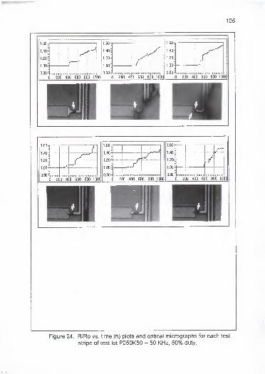
105
1 .60-
1.40-
1.20-3
1.00
0.80 TTrrriipmm jiinin^iiTmT|mrm|
0 200 400 600 800 1000
0.60 ~Vfm mt) 1 1 n iii] timii | m u ii 1 1m ii i
0 200 400 600 800 1000
0.80 mni ipn in rymiiiTjmT ii r|rrnriT|
0 200 400 600 800 1000
1 .60-
1.40-
1 20-
1 .00-
0.80-
f
J
—r 1 1 1 1 ri TiriTIT
0 200 400 600 800 1000
1.60-
1.40-
1.20-
1.00-
0.80" M fTM l TTTTriT m in i irrrrr r TltTli r
0 200 400 600 800 1000
I w
Figure 24. R/Ro vs. time (h) plots and optical micrographs for each test
stripe of test lot P050K50 - 50 KHz, 50% duty.
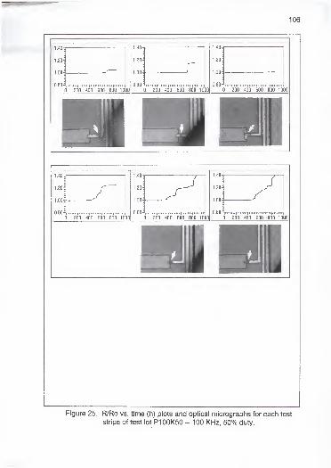
1.40'
1 .20-E
1.00 \
0.80=1 11
1 1 | 1 1 ii m 1 1 1 1 1 1 1 ii | itinn
0 200 400 S00 800 1000
1 .40
1 .20-=
1 .00-=
0.80=,
r1 1 1 1
11 1 1 1 1 1
11 it i i i j 1 1 1 1 1 npiii 1 1
1
1
0 200 400 600 800 1000
1.40-
1.20=
1.00-
0.80= , iimifi n i rr | 1 1 in ii 1 1 1 1 r i 11
1
0 200 400 600 800 1000
1.40ti
1.20-E
1.00=
0.80 = n it 1 1 1 1 1 1 11
1 in t •• IJ
1 1 1 1 1 111
0 200 400 600 800 1000
1.40-a
1.20=
1.00
0.80 T 'I"" 1 "! 1 1 1 1 1 1 i| im 1 1
1
0 200 400 600 800 1000
1.40^
1.20
1.00
0.80=1 11
1 1 t| 1 1 1 1 1 1 1 1 1 1
1
1
0 200 400 600 -800 1000
Figure 25. R/Ro vs. time (h) plots and optical micrographs for each test
stripe of test lot P100K50 - 100 KHz, 50% duty.
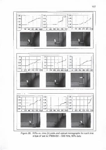
107
Figure 26. R/Ro vs. time (h) plots and optical micrographs for each test
stripe of test lot P500K50 -- 500 KHz, 50% duty.
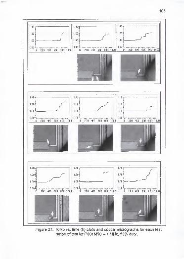
1.40
1.20-3
1.00
0.80-
1in i| 1 1 1 1 1 1
11 1 1 1 1 1 1 1 1 1 r |l M 1 1 1 1 (
0 200 400 600 800 1000
1.40
1.20
1 00-|
0.80-= n i 1 1 11
1 1 1 1 1 1 1 1[ 1 1 1 1 1 1 1 1 1 1 1 1 1 1
11 1 1 i iii
0 200 400 500 800 1000
1.40-
1.20^
1 on-;
0.80^,,,
0 200 400 600 800 1000
I 1 1 I II
I 1 1 I t 11
1 I I I 1 1 I I | I I I I I • I • • I I I 1 I 0.80 ~\ I II MMI
I I II II IIIIIIIM
|I 1 | Il|
0 200 400 600 800 1000 0 200 400 600 800 1000|
1 1 1 11
1 1 1 ii in | in n 11
1 1 1 1 1 1 1
1
1
0 200 400 600 -800 10001
1.40-
1.20|
1.00
0.80 I 0.80 1 1 1 1 1 1 11
1 1 1 1 1 1 11
1 mi ii i 1 1 m 1 1 it pill 1 1 1) 1 U.UW ~1 ii i itii|i 1 1 1 1 1 fii ii i n 1 1 1 1 ii 1
1
1
0 200 400 600 800 1000 0 200 400 600 800 1000 0 200 400 600 800 10001
Figure 27. R/Ro vs. time (h) plots and optical micrographs for each test
stripe of test lot P001M50 - 1 MHz, 50% duty.
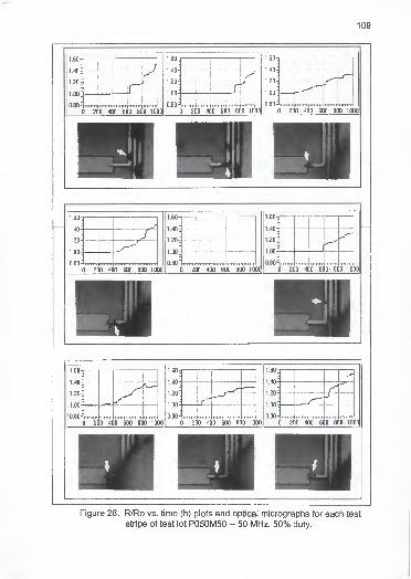
109
Figure 28. R/Ro vs. time (h) plots and optical micrographs for each test
stripe of test lot P050M50 - 50 MHz, 50% duty.

110
Figure 29. R/Ro vs. time (h) plots and optical micrographs for each test
stripe of test lot P133M50 - 133 MHz, 50% duty.
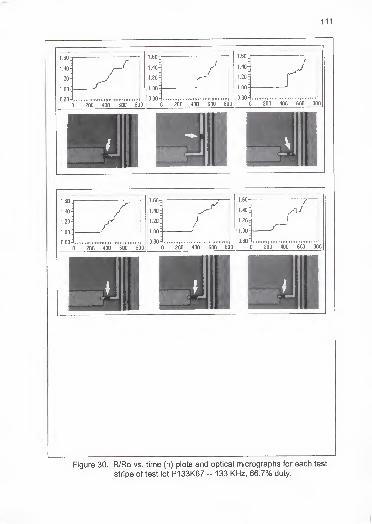
Figure 30. R/Ro vs. time (h) plots and optical micrographs for each test
stripe of test lot P133K67 -- 133 KHz, 66.7% duty.

112
Figure 31. R/Ro vs. time (h) plots and optical micrographs for each test
stripe of test lot P667K67 -- 667 KHz, 66.7% duty.
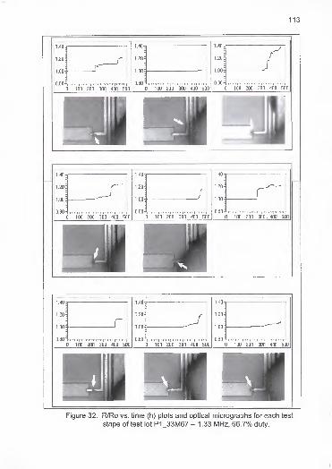
113
Figure 32. R/Ro vs. time (h) plots and optical micrographs for each test
stripe of test lot P1_33M67 -- 1.33 MHz, 66.7% duty.
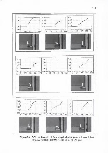
114
1.60-
1.40-
1.20:
1.00
I
0.80- ni irrm 11 1 ri 1 1 m|m 1 1 m 1 1 1 1 »tm t 1 1
1
0 200 400 600 800
1 .60-
1.40-3
1.20
1.00
0.80
0
trm-fiitTm-ir
400 600 800
1.60'
1.403
1.20
1.00
0.80 -tt imm | n it n Tir| i ii TTrTTT p fiin i n
0 200 400 600 800
1.60
1 00-
0.80-
1
i _ —4 -
tt rrvn ii-jn ttti ttt i i i mrn jnrnn 1
1
1.60-
1.40-
1 20
1.00:
0.80
j :
rr|-' n *T 'r~r n~rj i i f i | i r i
50 100 150 200 250
1.60-
1.40-
1.203
1.00
0.80- i rrm i rpni tit T 1 irn I inn qiimi rrr
200 400 600 800
1.60:
MO-
1.20:
1.00-
0.80
0 200 400 600 800
O.8O-1iTrirmrpi hitmin i itt n r| iti ittti
0 200 400 600 800
0.80 ^ • i niini frrri » i iti |t*ittttittittt it
t
t i ^
0 200 400 600 800
Figure 33. R/Ro vs. time (h) plots and optical micrographs for each test
stripe of test lot P067M67 - 67 MHz, 66.7% duty.

115
MO-
1.204
1.00
0.804
100 200 300 40CM500
1.40
1.20=
1.00
0.80
0 100 200 300 400 500
1.40-
120-f
1.00-f
(0.80 =
0 100 200 300 400 500
1.40
1.201
1.00
0.80-
ff I I 1 | 1 I I I | I i I | I I I l*| I I I 1 i
0 100 200 300 400 500
1.40
1.20
1.004-
0.80-=
I
i r t i - i i i i | i i i
0 50 100 150 200 250
1.40-
1 20-E
1 .00-=
0.80 =
:
0 100 200 300 -400 500
1.40-
1 20-
1.00-
0.80-
0 100 200 300 400 500
1 .40
1.20-
0.80
_ ! _ i :
0 100 200 300 400 500
1.40-
1.20-j
1.00=
0.80
0 1Q0 200 300 400 500
Figure 34. R/Ro vs. time (h) plots and optical micrographs for each test
stripe of test lot P133M67 - 133 MHz, 66.7% duty.
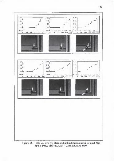
200' 300
' 400 500
1.60
100 200 300 400 '500
1.60
100 200 300 400 500
Figure 35. R/Ro vs. time (h) plots and optical micrographs for each test
stripe of test lot P160K80 -- 160 KHz, 80% duty.
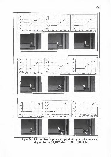
117
CD
/|
] 100 200 3(
1 1
1
)0 4(
rr 1
1
0 5C
0.80 ~\ 1 TT1 t"T T 1 r T ' 1 T-1T0 100 200 300 400 500
n| n r ipT it r | i rti |i i
0 100 200 300 400 500
J
1.60-
1.40-
1.20-
1 .00-
0.80J1 1
i
"' i
1 1 1 1'
' i'
0 100 200 300 400 500
r i t ft rn j i i i ryi-i i f | i'i tt
0 100 200 300 400 500 0 100 200 30Q 400 500
1.60'
1.40
: 20
1.00
0.80 i t i i | m-iT' i ri | i t f—r—f i i * r
0 100 200 300 400 500
1.60-
1.40-;
1.20t
1.00
0.80-
h
" rp ' ' ''H -i'ti n j rrrr fri n 1
0 100 200 300 400 500
1 .60
1.40:
1.20t
1.00
il
i i i "iir i~r i ft r~n~f
0 100 200 300 400 500
Figure 36. R/Ro vs. time (h) plots and optical micrographs for each test
stripe of test lot P1_60M80 -- 1.60 MHz, 80% duty.
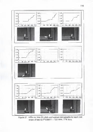
118
Figure 37. R/Ro vs. time (h) plots and optical micrographs for each test
stripe of test lot P133M77 -- 133 MHz, 77% duty.

119
1.40;
1.204
1.00
0.80 l i iJ
i i l i|
l i i l|
i l l i|
i i i r|
0 50 100 150 200 250
1.40-
1.204
1.0O-E
0.80-
0 50 100 150 200 250
1.40-
1.20-=
1.00- t.
0.80-
0 50 100 150 200 250
1.40-
1.20'
1.00-=
0.80J
50 100 150 200 250
1.40'
1.20
1.00
0.80'
0 500 1000 1500 2000 2500
1 .40-
1.20-
i ,oo-:
0.80
0 SO 100 150.200 250
1.40-
1.20-
1.004
0.80- 1 1 1 1 1 1 1 1 1 rt p n n -nm-J
0 50 100 150 200 250
1.40-
1.20
1.0O€
0.80-
0 50" ioO 150 "2OO 250
1 .40-
1.204
- 00
0.80
50 "l00 150 200 250
Figure 38. R/Ro vs. time (h) plots and optical micrographs for each test
stripe of test lot DC - DC.
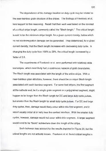
120
The dependence of the damage location on duty cycle may be related to
the near-bamboo grain structure of the stripes. The findings of Frankovic et al.
lend support to this reasoning. Recall that their work was based on the concept
of a critical stripe length, commonly called the "Blech length." The critical length
is said to be the minimum stripe length, for a given current density, below which
no net electromigration damage can be generated. They determined, for a given
current density, that the Blech length increases with decreasing duty cycle. In
changing the duty cycle from 100% to 25%, the critical length increased by a
factor of 2.6.
The experiments of Frankovic et al. were performed with relatively wide
test stripes, which most likely had a continuous network of grain boundaries.
The Blech length was associated with the length of the entire stripe. With a
near-bamboo grain structure, however, there should be a unique Blech length
associated with each bamboo segment. For some test stripes, the first segment
at the cathode end, be it a single grain segment or a polygrained segment, might
happen to be longer than the Blech length for DC and large duty cycle pulses,
but shorter than the Blech length for small duty cycle pulses. For DC and large
duty cycles, then, damage would likely occur within this first segment, and it
would usually occur at or very near the contact interface. With the smaller duty
cycles, however, damage would not occur within this segment. A larger segment
would need to be "found" somewhere down the length of the stripe.
Such behavior may account for the results depicted in Figure 20, but the
critical lengths are not actually known. Frankovic et al. found critical lengths in

121
their experiments on the order of tens of micrometers. The current densities
used in that study were around 5x10⁵A/cm
2. The pulse amplitude of 15 mA
used in the present work is equal to a current density of about 2.7x1
0
6A/cm
2in
the stripe and about 4x10⁶A/cm
2at the tungsten plug contact interface (the plug
cross section was 0.6 fam x 0.6 jam). Since jl c is constant, other things being
equal, a Blech length on the order of a few micrometers would not be out of the
question for the present work, and the length increments defined in Figure 20
are about 2.5 ^im. Admittedly, it is not strictly correct to assume that other things
are equal in comparing the two studies. For example, the test stripes used by
Frankovic et al. were pure aluminum, whereas an aluminum-copper alloy was
used in the present study. Their test temperature was the same (200 °C). In
any case, the above discussion offers a reasonable explanation for the results
and reveals an interesting topic for future work.
The time that was required for post-test deprocessing of the samples for
cross-sectional inspection prohibited such analysis on all stripes. Scanning
electron micrographs were obtained in cross-section for a few stripes, however,
and two are presented in Figure 39. The orientation of these micrographs is
opposite to that of Figures 21 through 38, that is, the downwind direction is from
right to left. The magnification was about 12000X.
Figure 39(a) reveals voiding above the tungsten contact, damage which
would have been assigned to the 1st increment in Figure 20. In Figure 39(b), no
damage can be seen at the tungsten plug, but some is evident farther downwind,
within the 2nd and 3rd increments. An interesting feature of the depleted areas

Figure 39. Cross-sectional SEMs of two tested stripes. The pulse
duty cycle was 80%.

123
is their blocked appearance. Three such blocked areas are evident in Part (b),
and their close spacing invites speculation on the Blech length. If the righthand
edge of any given block is the upwind end of a bamboo segment, then it might
be estimated that the length of the bamboo segment is equal to or less than the
distance from its upwind edge to the upwind edge of the next block to the left.
The Blech length, in turn, must be equal to or less than this measured distance,
which is about 1 for the distance, L, in Figure 39(b). The stripes pictured in
Figure 39 were tested with a pulse duty cycle of 80%, a value for which the
Blech length would be relatively small.
Two more cross-sectional SEMs are presented in Figure 40. These are
more highly magnified (-35000X) and center on the tungsten plug contact. The
test current was DC, and it flowed from left to right in these pictures. In addition
to the SEM, the corresponding top view optical micrograph and R/Ro versus time
plot are included in each of Parts (a) and (b).
Part (a) reveals damage above the contact, and the R/Ro plot indicates
an increase in resistance of about 7%. The optical micrograph shows a dark
region just at the contact area, in agreement with the SEM. It is interesting to
note the voiding that occurred at the left end of the test stripe, to the left of the
current path. The migration of material from this region was not caused by the
electron wind. Apparently, it was caused by the concentration gradient created
by the electromigration-induced depletion of material directly above the contact.
Part (b) of Figure 40 shows a test stripe for which powering was shut
down before the damage could proceed past the contact. The corresponding

124
Figure 40. Cross-sectional SEMs of two tested stripes. The test
current was DC.
(a) Damage above the tungsten contact.
(b) Damage at the leftmost edge, but not above the contact.
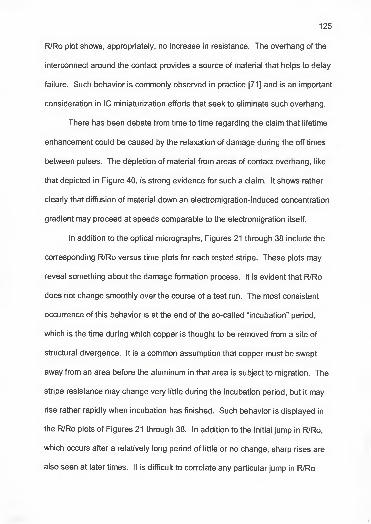
125
R/Ro plot shows, appropriately, no increase in resistance. The overhang of the
interconnect around the contact provides a source of material that helps to delay
failure. Such behavior is commonly observed in practice [71] and is an important
consideration in IC miniaturization efforts that seek to eliminate such overhang.
There has been debate from time to time regarding the claim that lifetime
enhancement could be caused by the relaxation of damage during the off times
between pulses. The depletion of material from areas of contact overhang, like
that depicted in Figure 40, is strong evidence for such a claim. It shows rather
clearly that diffusion of material down an electromigration-induced concentration
gradient may proceed at speeds comparable to the electromigration itself.
In addition to the optical micrographs, Figures 21 through 38 include the
corresponding R/Ro versus time plots for each tested stripe. These plots may
reveal something about the damage formation process. It is evident that R/Ro
does not change smoothly over the course of a test run. The most consistent
occurrence of this behavior is at the end of the so-called "incubation" period,
which is the time during which copper is thought to be removed from a site of
structural divergence. It is a common assumption that copper must be swept
away from an area before the aluminum in that area is subject to migration. The
stripe resistance may change very little during the incubation period, but it may
rise rather rapidly when incubation has finished. Such behavior is displayed in
the R/Ro plots of Figures 21 through 38. In addition to the initial jump in R/Ro,
which occurs after a relatively long period of little or no change, sharp rises are
also seen at later times. It is difficult to correlate any particular jump in R/Ro

126
with any particular damage site, but it might be estimated that the common
observation of more than one damage site is evidence that each jump in R/Ro
indicates the end of incubation at a different structural gradient.
Lifetime Data
The standard quantitative basis for comparing electromigration behavior
is tso. It is this quantity that most models strive to predict. The concern here is
the dependence of tso on the frequency and the duty cycle of a pulsed stress
current for a given temperature and pulse amplitude.
Figures 41 through 58 contain the raw data, extracted failure times, and
lognormal failure plots for each of the 18 electrical stress treatments. Part (a) of
each figure contains 6 to 9 R/Ro versus time plots, one for each test stripe in
that treatment lot. These plots are the same ones that were included with the
optical micrographs, earlier. Part (b) of each figure is a table of the failure times,
listed in ascending order for two failure criteria -- R/Ro = 1.10 and R/Ro = 1 .20.
These times were extracted from the plots of Part (a). The last column of the
table, headed "tso (h)," contains the median failure time for each failure criterion.
This median time was calculated by taking the logarithm of every failure time,
finding the mean of these log-times, and computing the inverse logarithm of this
mean. Such a method assumes, of course, that the failure times adhere to a
lognormal distribution. Part (c) of each figure is a plot of the Part (b) failure
times on a logarithmic time axis versus cumulative failure probability in percent.
Because failure times are assumed to be distributed lognormally, the plots
given in Part (c) of each figure should indicate linearity. In fact, it is common to

127
estimate tso for a group of failures by fitting a straight line to the given failure plot
and finding the intersection of this line with the 50th percentile on the probability
scale. Excellent linearity is often evident in Figures 41 through 58, but there are
also many cases in which it would be difficult to fit, with confidence, a straight
line to the data. The lack of consistent linearity is one reason that tso was not
estimated with this method, in addition to the fact that such a method does not
provide the best estimate, anyway. The best estimate is given by the calculation
described above.
The sometimes discontinuous behavior of the R/Ro data is reflected in the
failure plots. It can be seen in many of the plots that the apparent slope for one
R/Ro failure criterion is different from that for the other criterion. The data tend
to merge at larger failure times, which reflects a tendency for the discontinuous
jumps in R/Ro to be smaller for early failures than for late failures. Whenever a
sample "lives" for a relatively long time, it is more likely to eventually experience
a large jump in R/Ro. In such an instance, the failure time that is found using an
R/Ro failure criterion of 10% may be essentially the same as that which is found
using a criterion of 20%. Depending on whether one is primarily interested in
early failures, median failures, or late failures, this behavior may be of significant
practical concern regarding the selection of a failure criterion.
The apparent slope exhibited by a failure plot is essentially the standard
deviation of the failure times. An estimate of the standard deviation, which can
be performed graphically, is given by logftWtie), but it is more appropriate to
calculate it from its definition. It is normal practice to report the sample standard
128
(a) R/Ro versus Time in Hours P133K331.60-
"~5o6" VoVo" YsOO 200o' 2500
1.60
[(111 i~f-i~r 1 1 1 r 1 1 1 1 1 1 1
500 1000 1500 2000 2500
1 .60
1.40-]
1.20
1.00
0.80-v 1 1 r 1 1 1 1 1 1 1 1
0 500 1000 1500 2000 2500
1 r 1 1 1 1 1 1 1 1 1 1 1
0 500 1000 1500 2000 2500
1.60-
^.A0-
1.20:
1.00
0.60 Tin in 1 • mn 1 1niiiir|Tiiii iifriTi it
0 200 400 600 800 1000
1.60-
1.40:
1.20
1.00
0.80- mitit [in 1 nijin 1 1 n
0 200 400 600 800 1000 400 600 800 1000
(b)
Criterion Failure Times in Hours t»(h)
R/Ro=1.10 665 671 1078 1268 1317 1552 1038
R/Ro=1.20 916 1022 1317 1330 1331 1553 1225
Failure Time Distribution » P133K331600
1400
1200
_1000& 900
I 800
H 700
600
•
• 8 •
R/F 1.20• O
• R 'Ro=1 )
O O
(c)
5 10 20 30 50 70 80 90 95 99Cumulative Failures (%)
Figure 41 . Data for sample lot P1 33K33 - 1 33 KHz, 33.3% duty cycle.
a) R/Ro versus time plots for each of the 6 samples.
b) Failure times for the failure criteria R/Ro=1.10 and R/Ro=1.20.c) Log-normal plot of failure times for each criterion.
129
(a) R/Ro versus Time in Hours P667K33
'500 10001 1 1 1
1
f
1500 2000 2500» T I T II I I I TTT I fill
1000 1500 2000 2500
ri r~i |~nx t f~t 1 1 1 | 1 1 1 1 1 1 1 1 1 f
500 1000 1500 2000 2500]
1500 2000 2500' 1 • 1 1 '
• '' 1 " 1
1000 1500 2000 2500
1 1 up ill I 1 n 1 [i 1 r ? f ri~
500 1000 1500 2000 2500
1.60
1.403
1.20
1.00}
0.80
1.60
1
BOoTooV 1500 2000 2500
1.00
J0 500 1000 1500 2000 2500 10 2000 2500
(b)
Criterion Failure Times in Hours t5o(h)
R/Ro=1.10 836 861 873 876 920 958 1063 1072 1565 984R/Ro=1.20 975 1026 1068 1087 1138 1170 1287 1305 1565 1169
Failure Time Distribution - P667K3316001500
1400
_ 1300
£ 1200CD
E 1100H
1000
900
800
i •
R/R0= 1.20
>•
•• D O
•__ C
)°
D O O R/R0= 1.10
(c)
1 5 10 20 30 50 70 80 90 95 99Cumulative Failures (%)
Figure 42. Data for sample lot P667K33 - 667 KHz, 33.3% duty cycle.
a) R/Ro versus time plots for each of the 9 samples.b) Failure times for the failure criteria R/Ro=1.10 and R/Ro=1.20.c) Log-normal plot of failure times for each criterion.
130
(a) R/Ro versus Time in Hours P133M331.60
0.80 —\ 1 1 i 1 1 n i 1 1 r iTTp i i r i t t 1 1-
0 500 1000 1500 2000 2500
1.60
1.40-
1.20-E
1.00
0.80" T i I I ^ i i rrfrr i I | I I I I | I I I I
0 500 1000 1500 2000 2500
O.BO^'i ttt"| 1 1 n | n i i1
1 i 1 1 | n ii|
0 500 1000 1500 2000 2500
1 60
1.40
1.20
1.00-
0.80-
1.60
1.40:
1.20:
1 00
0 500 1000 1500 2000 2500
0.80 riTrfiTrrfn i i p'T iT fi i 1
1
0 500 1000 1500 2000 2500
1.60
500 1000 1500 2000 2500
0.80*^ n n | i i i i | i i i i | i i n f-rn0 500 1000 1500 2000 2500
1.60 1.60
0.80 -y-r i 1 1 inn500 1000 1500 2000 2500
1.00
0.80
y
0 500 1000 1500 2000 2500
Criterion Failure Times in H ours tso(h)
R/Ro=1.10 596 724 799 833 1120 1150 1244 1547 959R/Ro=1.20 890 915 1065 1140 1270 1305 1445 1585 1180
Failure Time Distribution ~ P133M331600
1400
1200
_1000S 900® 800
P 700
600
500
*/Rc =1 20 V»»
f '
—
R/R()=1 .10
c(
>
o
(c)
1 5 10 20 30 50 70 80 90 95 99Cumulative Failures (%)
Figure 43. Data for sample lot P1 33M33 - 1 33 MHz, 33.3% duty cycle.
a) R/Ro versus time plots for each of the 8 samples.b) Failure times for the failure criteria R/Ro=1.10 and R/Ro=1.20.c) Log-normal plot of failure times for each criterion.
131
(a) R/Ro versus Time in Hours P050K501.60
J 1 I I I ITfTfTlTrrtlf IIIIIITf TIT11 I1|T1I1 1TI
0 200 400 600 800 1000
1.B0-
1.40-
1 20
1.00-
0.80- III 1 1 1
1
i mriT II Dili 0.80- ,„„ pTTiiTlpifiiii jtitiinjTiinii]
0 200 400 600 800 1000
1 60
0 2Qr
0 400 eoT'so'ir'i'oOO
rrrr|t f ? i rn] trmnpiirnTp-inri r
0 200 400 600 800 1000
1.60
030 ~yi ttTTfT|TiTrtTrprrrtrrrptrrr tt|tiirrn
0 200 400 600 800 1000
1.60
1.40 :
1.20:
1.00:
0.80 miff mrnfnrim jiiui iqimrrr
0 200 400 600 800 1000
1.60-1-
1.40:
1.20:
1.00:
0.8o4..
1.60-
0 200
(Tirtrii|ttttt i rfiiii in]
400 600 800 1000
1.40:
1.20:
1.00
0.80J nriiitp mum] iiiiiii pun ii f i|
0 200 400 600 800 1000
(b)
Criterion Fai ure Times in Hours tso(h)
R/Ro=1.10 437 440 515 537 538 595 507R/Ro=1.20 525 550 565 627 650 692 598
Failure Time Distribution - P050K50700
650
600
— 550o
p 500
450
400
•
VRo=1.
•
••
—
F
20•
o
• OoR/R(
O)=1 ,10
O O
(c)
5 10 20 30 50 70 80 90 95 99Cumulative Failures (%)
Figure 44. Data for sample lot P050K50 - 50 KHz, 50% duty cycle.
a) R/Ro versus time plots for each of the 6 samples.
b) Failure times for the failure criteria R/Ro=1.10 and R/Ro=1.20.c) Log-normal plot of failure times for each criterion.

132
(a) R/Ro versus Time in Hours P100K501.40-
1.201
ami
0.80 ni mi|immf mini piin iipiii ittj
0 200 400 S00 800 1000
1.40tt
r^riTTITTlIlium Tniin i 1 1 1 1 1 1 nTTfi
\
0 200 400 600 800 1000
1.40-j
1.201
1.00-=
0.80-1 titiiii |i i him 1 1111111 1 1 nt i Ti]rntTii(
0 200 400 600 800 1000
1.40
1.20
1.00
0.80
o Hao
1.40^
vmi
1.00
1 1
1
1 1 1I 1
1 1 1
400 600 800 1000
1 40
0.80~^m in iinun t|mrinpm i min im
0 200 400 600 800 1000
1.201
1.00
0.80
1.40-
1201
1.001
0.80
0 200
miput ii 1 1 1 1m Trfnrrrrri
400 600 800 1000
1.40
1.201
1.001
Q.80~Vrr inr|TTinu [ limn |t mi
0 200 400 600 800 1000
tTflf i n
1
1 [ i
r
u in prm rtpTir
0 200 400 600 800 1000
1.40tt
0.80-
0 200 400 600 800 1000
(b)
Criterion Failure Times in H ours t5o(h)
R/Ro=1.10 514 540 570 718 640R/Ro=1.20
Failure Time Distribution - P100K50750
700
— 650
<D
E 600i-
550
500
o
o R/Rc)=1 .10
oo
(c)
1 5 10 20 30 50 70 80 90 95 99Cumulative Failures (%)
Figure 45. Data for sample lot P1 00K50 - 1 00 KHz, 50% duty cycle.
a) R/Ro versus time plots for each of the 6 samples.b) Failure times for the failure criteria R/Ro=1.10 and R/Ro=1.20.c) Log-normal plot of failure times for the criterion R/Ro=1.10.
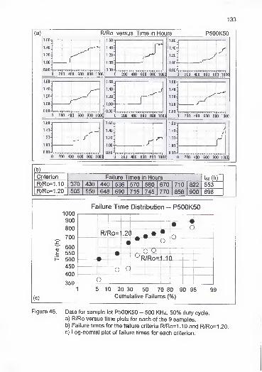
133
(a) R/Ro versus Time in Hours P500K501.60
1.40-j
1.20
1.00
0.80 i n mn ii niTu im iitHttti i iipun rff
0 200 400 GOO 800 1000
1.60-
0.80-i„ rriiiji irrnT|TTTTm~fi itttn|n rr ri i \
0 200 400 600 800 1000
0.80- ITfl 1 1 1 1 1 1 1 IIIITI1 [IIIII 11|TlirTT
T
0 200 400 600 800 1000
1 60
1.40-]
1.20
1.00
0.80
1.60
iTn|i mil 1 1 inrirrr itiii ufiiirni
|
0 200 400 600 800 1000
Q.8Q ~^tii nnpTTi rn ; n itiii
0 200 400 600 800 1000
1.60
1.40
1.00
0.80-1 fill II Mill
0 200 400 600 800 1000
1.60 :
1.40:
1.20:
1.00-
0-80 ~) tnmrp-
| inn | nmn0 200 400 600 800 1000
1.60- 1.60
1.40:
1.20
1.00
n i tin)rrmr rfT iTTTTrpTiTTTTfinnn0 200 400 600 800 1000
0.80- tiTfvnmiT inmiintrr ii|irn ur
0 200 400 600 800 1000
(b)
Criterion Failure Times in Hours tso(h)
R/Ro=1.10 370 430 440 536 570 580 670 710 822 553R/Ro=1.20 505 550 648 690 715 745 770 858 900 698
Failure Time Distribution - P500K50
<D
E
1000
900
800
700
600550500
450
400
350
• rR/Ro=1 .2()
i^• O
• 0
• ) o< /Ro='L1(1
O—
3
(c)
1 5 10 20 30 50 70 80 90 95Cumulative Failures (%)
99
Figure 46. Data for sample lot P500K50 - 500 KHz, 50% duty cycle.
a) R/Ro versus time plots for each of the 9 samples.b) Failure times for the failure criteria R/Ro=1.10 and R/Ro=1.20.c) Log-normal plot of failure times for each criterion.
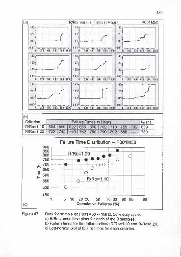
134
(a) R/Ro versus Time in Hours P001M501.40-
1.20-|
1.004
0.B0 *"imiiii|i Hiiii|iintrr|ii i rrn 1 1 1 1 in
0 200 400 600 800 1000
1.40q
1.20
1.00-E
0.80-1,,,.,. « ] « I l i t Iimi in |TTTTT1I
II 1 1 I I I I
i
0 200 400 600 800 1000
1.00-
0.80^I" 1
1 1 1 1 1 1 1 inriTTi mi in
1.40
1.20
1.00
0.80
/""1 ""1rTTTTTTTl
1.40-
1.20
1.00-
0-80 — ti 1 1
1
n |i im rt [ 7it 1
1
ntttt ruft»n rrn j
0 200 400 600 800 1000
1.40
1.20
1.00
0.80 ' ni fnnru t M i| i iiiiii pun njiirn r
0 200 400 600 800 1000
1.40-
1.20|
1.00
1.40
0-80 \%\\ 1 1 11
1 1 Tirrii| rmiM i ui 1 1 iipi fi or
0 200 400 600 800 1000
1.40-
0 200 400 600 800 1000
1.00-j-
O.BO^n [linn 1(111mi | T 1 1 1 1 ||
0 200 400 600 800 1000
(b)
Criterion Fai ure Times in Hours tso(h)
R/Ro=1.10 504 550 622 665 690 702 710 755 792 659R/Ro=1.20 702 742 749 762 765 790 802 858 780
Failure Time Distribution - P001M50900850800750
p 700
© 650
j| 600
550
500
450
R/Ro=1J2Q
o--I• 0
C
O R/Ro==1.10
r
(c)
1 5 10 20 30 50 70 80 90 95Cumulative Failures (%)
99
Figure 47. Data for sample lot P001 M50 -- 1 MHz, 50% duty cycle.
a) R/Ro versus time plots for each of the 9 samples.
b) Failure times for the failure criteria R/Ro=1.10 and R/Ro=1.20.c) Log-normal plot of failure times for each criterion.
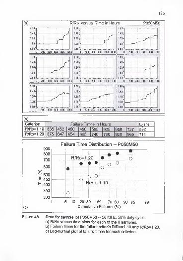
135
(a) R/Ro versus Time in Hours P050M501.60
1.40-
1 20^
1.00
0.80 rTTTI |1 1 1 111 1 1 1111111 [IITTTIIpIII TTT
200 400 600 800 1000
1.60-
1.20
1.00
0.80i„ti i iiiip iiitii) ii mil |irrrrti|iitiTTii
0 200 400 600 800 1000
1.60-
1.00
0.80-1, 1 1 II1T|T ITT111
1
0 200 400
rrrrtrn i ttiii 1
1
600 800 1000
1 60
1.40
1.20-
1.00-
200 400 600 800 1000
0.80 1 1 1 1 1 1 1 1 1 1 1 1 1
1
0 200 400 600 800 1000
1.60
0.80- > | I M I l I I | 1 I I I I
200 400 1000
1.60-
TT|"TTTTITF JVTT1 I Tl|FIfTITT
200 400 600 800 10000.80 ~~\ni iiiif i ii pi ii| mini jTiiTnijiTii in
0 200 400 600 800 1000
1.60
0.80-Vrrrr
0 200 400 600 800 1000
(b)
Criterion Failure Times in H ours tso(h)
R/Ro=1.10 335 452 480 490 595 635 658 727 532
R/Ro=1.20 575 647 654 665 740 790 820 865 714
Failure Time Distribution - P050M50900
800
700
600
f 500
E 450F 400
350
300
>
1ft 1
*'
FVRo =1. 20 o1 • <1 •
o c>1
•
C/Ro=1.10
O
(c)
1 5 10 20 30 50 70 80 90 95Cumulative Failures (%)
99
Figure 48. Data for sample lot P050M50 - 50 MHz, 50% duty cycle.
a) R/Ro versus time plots for each of the 8 samples.b) Failure times for the failure criteria R/Ro=1.10 and R/Ro=1.20.c) Log-normal plot of failure times for each criterion.
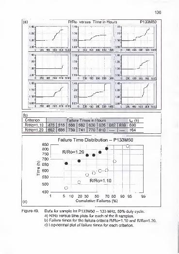
136
(a) R/Ro versus Time in Hours P133M501.40-
1.20-1
imh
0.80- > > 1 11
1 i | 11
1 1
1
0 200 400 600 800 10001
1.40|
1.20 4
1.004
0 .8
0
~\n titirfnTTTiTf iiiiiii (inn iF|rnTTT
0 200 400 600 800 1000
1.204
1 .00-=
0.80-v..t,t,tp 1 1 1 iir
| iiiiiii|
0 200 400 600 800 1000
1.40
1.20
1.00-
0.80-
I
1.40
1.20^
1.004
0.80
0 200 400 600 800 1000
IIII M I| |IU T IM |III I 1
0 200 400 600 800 1000
I.4O-3
1.204
1.00-E
0.80** ni i ni |i ii u i > | n i i Tu [m ii npn i
0 200 400 600 800 1000
1.40
1.20-=
1.004
0.80~\TTI 1 1 1 1 IT| ITinTT J1TTTTII|TI 1 1 TIT
0 200 400 600 800 1000
0.80^ii. nii|iriiiii | ii |min i|mmit0 200 400 600 800 1000
1.40
1.204
i.oo4-
0.80-1
0 200 400 600 800 1000
(b)
Criterion Failure Times in Hours tso(h)
R/Ro=1.10 475 515 568 582 600 605 682 838 600R/Ro=1.20 662 685 739 741 770 810 764
Failure Time Distribution - P133M50850
800
750
700
650
E 600i-
550
500
450
i— -oF )=1.; •
i •
• ip
o c)
—
c\>
°
c R/R 0=1/10
O
(c)
5 10 20 30 50 70 80 90 95Cumulative Failures (%)
99
Figure 49. Data for sample lot P1 33M50 - 1 33 MHz, 50% duty cycle.
a) R/Ro versus time plots for each of the 8 samples.
b) Failure times for the failure criteria R/Ro=1.10 and R/Ro=1.20.c) Log-normal plot of failure times for each criterion.
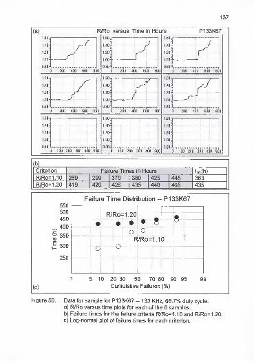
137
(a) R/Ro versus Time in Hours P133K671.60
200 400 600 800
ISO
\M-
1.20-j
1.00
0.80-1 i p tin rnipiirtiiir f 1 1
1
ittin
0 200 400 600 800
1.60-
1.40
1.20
1.00
0.80"" MTiiiiii pimrtirpn mni ptim irij
0 200 400 600 800
1 GO
1.40-
1.20-
1.00-
1.60
0.80~ riimm |
t
urn nnnnm in im iiiii
0 200 400 600 800 0 200 400 600 800 200 400 600 800
1.60-
0.80-
1.60
0 100 200 300 400 500
1.B0
1.40-;
1.20^
1.00^
0.80+,0 100 200 300 400 500
1.40^
1.20
1.009
0.80-1
0 100 200 300 400 500
(b)
Criterion Fai ure Times in Hours tso(h)
R/Ro=1.10 289 299 370 380 425 445 363
R/Ro=1.20 419 420 426 435 448 465 435
Failure Time Distribution - P133K67550
500
450
_ 400
f- 350
|| 300
250
K/ =1.20ft
• • • •
O OFJRo= 1.1 0
o O
(c)
5 10 20 30 50 70 80 90 95 99
Cumulative Failures (%)
Figure 50. Data for sample lot P1 33K67 -- 1 33 KHz, 66.7% duty cycle.
a) R/Ro versus time plots for each of the 6 samples.
b) Failure times for the failure criteria R/Ro=1.10 and R/Ro=1.20.c) Log-normal plot of failure times for each criterion.

138
(a) R/Ro versus Time in Hours P667K671.60
1 1 1 1 1 1 1 1 1 i
600 800
1.60-
0.80- „,,in 1 1 1 1 11
1
ii iriTinfmmm piiiir
200 400 600 800
1.60-
1 .40^1
1.20
1.00
0.80 "~^riTTnTTrfTTTrii iii|tii iimi |iiiiit ni|
0 200 400 600 800
1.60;
1.00-
0.80-
1
"1"" MIMUIIII in 1 1 n
n
fTTlTTT n ri
1.60
1.40-
1.20-3
1.00
200 400 600 800
0.80 ~V TT1 TITU I [I I II H IH |mTTtT1
0 200 400 600
rrrrf
800
1.60
1.40^
1.20^
1.00
0.80 iii n i l 11 1mi fl i rt]
200 400 600 800
1.60
TTTT
200
1.60-
nrmrrrpiun nipii 1 1 uTrpMfrnn
200 400 600 800
1.60
1.40-^
1.20^
1.00
0.80 rnimqTii in m[uiniin pimi it i
200 400 600 800
(b)
Criterion Failure Times in Hours tsofh)
R/Ro=1.10 245 259 274 349 372 378 394 413 475 343R/Ro=1.20 294 328 371 386 396 412 470 474 512 399
Failure Time Distribution - P667K67
550
500
450
400
350EH 300
250
200
Ro=• • c
Ri 1.20 o•
O
• R/Ro =1. 10
O C
I
(c)
10 20 30 50 70 80 90 95Cumulative Failures (%)
99
Figure 51. Data for sample lot P667K67 - 667 KHz, 66.7% duty cycle.
a) R/Ro versus time plots for each of the 9 samples.b) Failure times for the failure criteria R/Ro=1.10 and R/Ro=1.20.c) Log-normal plot of failure times for each criterion.
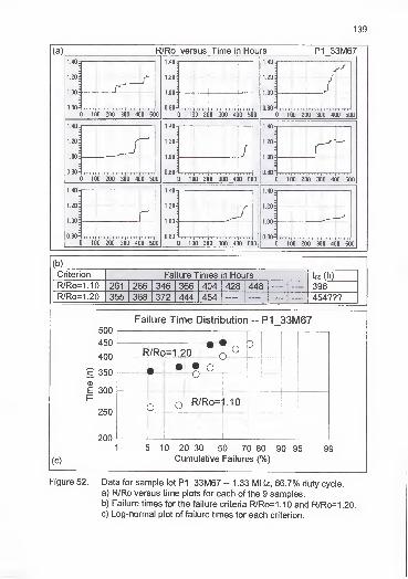
139
(a) R/Ro versus Time in Hours P1 33M671.40-
0.80" ii i i'| r itt] i i i i | r i 111 i it
0 100 200 300 400 500
1.40
1.203
1.00
0.80-Wi-rl I 'InnTTTi | I
|
0 100 200 300 400 500
0.80-^ , I 1 1 I i I i |n100 200 300 400 500
•j in l | i i i i f-rn T | i~i i i | i i i i
0 100 200 300 400 500
1.40
1.20
1.00
0.80 - -t
j
1.40
1.203
1.00
0.80
0 100 300 400 500
i i 1 1 t i r i-| n t i | i i i i | i i i
0 100 200 300 400 500
1.40-
1.00- r.
1.40
0 100 200 300 400 500
1.20-E
1.00
0.80
0 100 20C
I
'
300' 400 500
1.40
1.20-=
1.00
0.80 rTTTj1 " II II 1
Criterion Failure Times in Hours Wo (h)
R/Ro=1.10 261 266 346 366 404 428 448 396R/Ro=1.20 355 368 372 444 454 454???
Failure Time Distribution - P1 33M67500
450
400
g 350
E 300i-
250
200
F =1.2 0 •to >-
• • oc _
O R/Ro='1.10
(c)
1 5 10 20 30 50 70 80 90 95 99Cumulative Failures (%)
Figure 52. Data for sample lot P1_33M67 - 1 .33 MHz, 66.7% duty cycle.
a) R/Ro versus time plots for each of the 9 samples.b) Failure times for the failure criteria R/Ro=1.10 and R/Ro=1.20.c) Log-normal plot of failure times for each criterion.

140
(a) R/Ro versus Time in Hours P067M67I.BO-x
\A0-_
1.2*
\m\-
.BO- n rrrfTir] 1TI T1 I I I II
I Ii
] 200 400 600 800
1.60-
1.20
1.00
0.80 irrmrryrn 1 1 1 m|iii ii tin (iiim )i
0 200 400 600 800
1.60-
1.00
0.80-1,,, nun 1 1 imrffifiiin 1 1 11 |iiiui i ii|
0 200 400 600 800
1.60
140:
1.20:
1.00
0.80 ~i n iin ii
|ttt tti iTi|mu irii [iTiru Tr
0 200 400 600 800
1.60
1.40-
1.20:
1.00-j
0.80" tiii riT>r]T
i
h it iii[ 1 1 1 1 1m ilium
m
/
0 200 400 600 800
1.60
1.40
1.20-3
1.00
0.80" m riTiii | ii 1 1 1 1 n i ( iii mn rfiiii ii ii
0 200 400 600 800
1.60
1.40-
1.20:
1.00
0.80 Hn |in | mi0 200 400 600 800
1.60-
1.40^
1.20
1.00
0.80-1 1111 1 |HITnTTT1
0 200 400 600 800
1.60-
1.40-
1.20
1.00-
0.80"" in i iiiii 1
1
hi 1 1 iii|iiniiiir|Tiiiirnf
0 200 400 600 800
(b)
Criterion Failure Times in Hours feo(h)
R/Ro=1.10 238 254 272 303 352 377 388 520 328
R/Ro=1.20 341 356 360 385 429 429 447 534 406
Failure Time Distribution - P067M67550
500
450
_400— 350
|| 300
250
200
i
Ri Ro=1.2•
—
i
> • •rO
-C(
>
3 R/f*0=1. 10
o
(c)
1 5 10 20 30 50 70 80 90 95 99Cumulative Failures (%)
Figure 53. Data for sample lot P067M67 - 66.7 MHz, 66.7% duty cycle.
a) R/Ro versus time plots for each of the 8 samples.b) Failure times for the failure criteria R/Ro=1.10 and R/Ro=1.20.c) Log-normal plot of failure times for each criterion.

141
(a) R/Ro versus Time in Hours P133M67
1.00-E
III
III
1
1
0.80" n-rrr-i i i i | iri i | i i r i | i Tix-y
0 100 200 300 400 500
1.40
1.20
1
1.00
0.80 *"T nTi| 1 1 » i | i i t if r ri i 1 1 titj
0 100 200 300 400 500
1.40'
1.20-3
1.00
0.80" ii i i| r i i i f i i r i [ i n i nr0 100 200 300 400 500
1 40
1.20
1.00-
1.40 -j
0.80 i i i i| 1 1 np-i i i
ii i i i 1 1 i ii
0 100 200 300 400 500
1.00^
0.80 tttt rn ti fm tt r 1 11
1 1 1 1
1
1 1 1 1 1| r
0 200 400 600 BOO
1.40^f
1.20-3
1.00
0.80
0 100 200 300 400 500
1.40-
1.20|
1.00
0.80
1
1.40ri
"l n m | i i i rpjT T-7-TT t t |t t n~0 100 200 300 400 500
1.20|
1.00
0.80
1.40-
1.20-
1.00-
0 100 200 300 " 40o" 500
0.80 "\m t f il l i | 1 1 1 1l
1 in |i r r
0 100 200 300 400 500
(b)
Criterion Failure Times in HoursR/Ro=1.10 261 338 367 390 405 462 405R/Ro=1.20
Failure Time Distribution - P133M67500 r
450
400
Q)
E 350
h-
300
250
C)
O(
0p
cr RirRo=1 .1C)
0
(c)
5 10 20 30 50 70 80 90 95Cumulative Failures (%)
99
Figure 54. Data for sample lot P1 33M67 - 1 33 MHz, 66.7% duty cycle.
a) R/Ro versus time plots for each of the 8 samples.b) Failure times for the failure criteria R/Ro=1.10 and R/Ro=1.20.c) Log-normal plot of failure times for the criterion R/Ro=1.10.

142
(a) R/Ro versus Time in Hours P160K801.60-
1.00
0.80-
ii
iii
n
1 n •
.
rnrtl1
* ' < 1» 1 • 1
1
TTTT
1.60-
\.m*
1.20:
1.00
0.80-1 - I| II I I { I I I 1 p TI I"|TI'
100 200 300 400 500
1.60-
1.20:
1.00
0.80 J I I I I I I I I I I 1 I I II
I I > II
0 100 200 300 400 500
t i i i | r i r i | ii i I | T i i i fi i m100 200 300 400 500
1.60
1.40:
1.20:
1.00:
0.80 rrr|TrrqT ri i |i i ii |i i it
100 200 300 400 500 0 100 200 300 400 500
Till |TI 1 1|
100 200 300 400 500
(b)
Criterion Fai ure Times in Hours tso(h)
R/Ro=1.10 226 237 247 282 318 325 270
R/Ro=1.20 274 291 306 375 378 387 332
Failure Time Distribution - P160K80
450
400
350
© 300
250
200
• • •
R/Ro=1.2 0•l o O
•• o
R/Rci=1.1 0
Oo o
(c)
5 10 20 30 50 70 80 90 95 99
Cumulative Failures (%)
Figure 55. Data for sample lot P160K80 - 160 KHz, 80% duty cycle.
a) R/Ro versus time plots for each of the 6 samples.
b) Failure times for the failure criteria R/Ro=1.10 and R/Ro=1.20.
c) Log-normal plot of failure times for each criterion.

143
(a) R/Ro versus Time in Hours P1 60M801.60-
1.40-
1.20^
1.00
0.80" 1 1 rtfit iTfn t~rj rrnl rin0 100 200 300 400 500
0 .8
0
—\
- 1 1 1 1 1 1 1 1 1 1 1 1 1 1 1 1 » ii ji i ii
0 100 200 300 400 500
1.60
1"TT TTpi r i | i ii i | i i r | i ii {
0 100 200 300 400 500
1.60
1.40
1.20-]
1.00
0.80 ^ t i t i~pT~i T~i Ti-rrnryr tt rfnn0 100 200 300 400 500
0.80 -i i i i 1 1 * i i j 1 1 1 1 1 1 1 1 1 1 1 1
1
0 100 200 300 400 500
0.80 I I I I | I I I' I | I I I I | ITTT |TT~T1 1
0 100 200 300 400 500
1.60
1.40-3
1.20
1.00
0.80-
1.60-
1.40-]
1.20
1.00
_
in i| ii i i | r in ] rm0 100 200 300 400 500
0.80-
1.60
1.40
1.20
1.00-
TTT<
0 100 200 300 400 500
0.80J n i i r 1 1 t rj'n'Ti 1 1 i n0 100 200 300 400 500
(b)
Criterion Failure Times in Hours tso (h)
R/Ro=1.10 218 232 234 242 243 245 255 275 380 255
R/Ro=1.20 244 262 272 276 286 296 304 338 380 293
Failure Time Distribution - P1 60M80
Ei-
400
350
300
250
200
•
R/Fto=1.20
•
• •1•
oo
I
iO c oc) CJ
Ro=1 ,c
(c)
5 10 20 30 50 70 80 90 95 99
Cumulative Failures (%)
Figure 56. Data for sample lot P1_60M80 - 1 .60 MHz, 80% duty cycle.
a) R/Ro versus time plots for each of the 9 samples.
b) Failure times for the failure criteria R/Ro=1.10 and R/Ro=1.20.
c) Log-normal plot of failure times for each criterion.
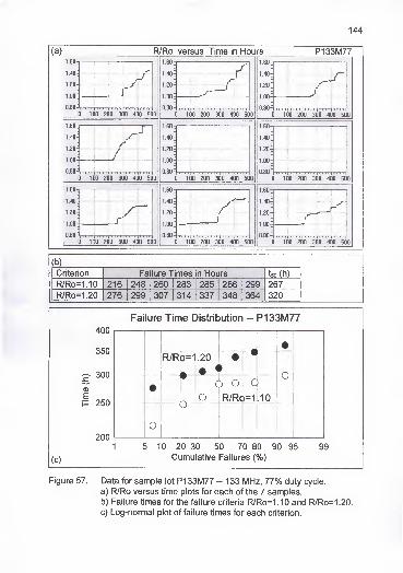
(a) R/Ro versus Time in Hours P133M771.60
1.40:
1.20^
1.00
0.80-1 n |tt i i | i
100 200
III J T T
300
i i 1 1 rrr
400 500
1.60
1.40^
1 20
1.00-
O.8O-1
,
100 200
iijii
300 400 500
1.60
1.40
1.20
1.00
0.80 1 1 r t|tttt"!" t~i r i | rrn 1 1 r i i
0 100 200 300 400 500
1.60
1.40
1.20-]
1.00
0.80 • i • i
100 200 300 400 500
1.60-
1.40
1.20-]
1.00-
0.80 -w0
r|'TT
100
1.60
1.40
1.20
1.00
0.80
200 300 400 500 0 100 200 300 400 500
100 200
TT| IT
100
1 1 1 I I
200 300 400 500
1.60
1.40
1.20
1.00
0.80 rrf i r rr\ ni i yvr i r p rrr
0 100 200 300 400 500
(b)
Criterion Failure Times in Hours
R/Ro=1.10 216 248 260 283 285 286 299 267
R/Ro=1.20 276 299 307 314 337 348 364 320
Failure Time Distribution - P133M77
E
400
350
300
250
200
•R/Ri .20
• <
4 i
•1
bo R/RC
C
)=1
1
.10
o
o
<
(c)
5 10 20 30 50 70 80 90 95
Cumulative Failures (%)
99
Figure 57. Data for sample lot P1 33M77 -- 1 33 MHz, 77% duty cycle.
a) R/Ro versus time plots for each of the 7 samples.
b) Failure times for the failure criteria R/Ro=1.10 and R/Ro=1.20.
c) Log-normal plot of failure times for each criterion.
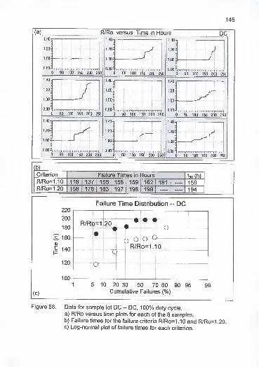
145
(a). R/Ro versus Time in Hours1.40-,
1.204
1.00
0.80" 1 1 i i ( n i 1 1 i 1 1 i 1
1
i 1 1 1 1 i 1 1 I
0 50 100 150 200 250
DC1.40-q
1.201
1.00
0.80" i !tt) ? m-| i i i i | i i rrfn it]
0 50 100 150 200 250
1.40
1.204
1.00
0.80^ i r it| 1 1 i 1 1 h i i 1 1 n 1 1n n0 50 100 150 200 250
1.40t
1.2041
1.00
0.80^..,,
.
, « rl
0 50 100 150 200 250
1.40
1.204
1.004
0-80 —1 1' 1 1 1 1 1 1
1
1
0 50 100 150 200 250
1.40t
1.40
1.20
1.00-
0-80" ii n|
i
n i | i i r i | i i i i )i i it-]
0 50 100 150 200 250
1.40-
1.204
1.00
I'-I'ili-'I |.f,| Hlll'l0.80~ -TTTTfn IT) 1 TTT|1 I I I j T I
0 50 100 150 200 250
0.80 i i i 1
1
1 1
1
[ 1 1
1
1 1 1 1 11
1 1
1
1 1
0 50 100 150 200 250
1.40
0 50 100 150' 200' 250
(b)
Criterion Failure Times in Hours tsoth)
R/Ro=1.10 118 137 155 158 159 162 181 159R/Ro=1.20 168 178 183 197 198 198 194
Failure Time Distribution - DC220
200
180
£. 160
I 140I-
120
100
,
1
R/R()=1 201 -A
•-«
0 c
0=1/
)
p-
(D OR/R 0
C>
Cr
(c)
1 5 10 20 30 50 70 80 90 95 99Cumulative Failures (%)
Figure 58. Data for sample lot DC - DC, 1 00% duty cycle.
a) R/Ro versus time plots for each of the 8 samples.b) Failure times for the failure criteria R/Ro=1.10 and R/Ro=1.20.c) Log-normal plot of failure times for each criterion.
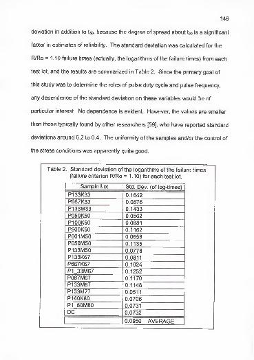
deviation in addition to tso, because the degree of spread about tso is a significant
factor in estimates of reliability. The standard deviation was calculated for the
R/Ro = 1.10 failure times (actually, the logarithms of the failure times) from each
test lot, and the results are summarized in Table 2. Since the primary goal of
this study was to determine the roles of pulse duty cycle and pulse frequency,
any dependence of the standard deviation on these variables would be of
particular interest. No dependence is evident. However, the values are smaller
than those typically found by other researchers [59], who have reported standard
deviations around 0.2 to 0.4. The uniformity of the samples and/or the control of
the stress conditions was apparently quite good.
Table 2. Standard deviation of the logarithms of the failure times
(failure criterion R/Ro = 1.10) for each test lot.
Sample Lot Std. Dev. (of log-times)
P133K33 0.1642
P667K33 0.0876
P133M33 0.1433
P050K50 0.0562
P100K50 0.0881
P500K50 0.1162
P001M50 0.0658
P050M50 0.1135
P133M50 0.0778
P133K67 0.0811
P667K67 0.1024
P1 33M67 0.1252
P067M67 0.1170
P133M67 0.1148
P133M77 0.0511
P160K80 0.0706
P1 60M80 0.0731
DC 0.0732
0.0956 AVERAGE

147
Relationships Between Lifetime. Pulse Frequency and Duty Cycle
We want to know how pulse frequency and duty cycle (or ton and toff) affect
the life of an interconnect when it is subjected to a pulsed stress current. In this
work, test stripe life has been characterized by the median time to failure, tso, for
a group of test structures. The data that were detailed in Figures 41 through 58
included, for 18 treatments, the individual times to failure and the median times
to failure for each of two failure criteria, R/Ro=1.10 and R/Ro=1.20. Figures 59
through 66 present those tso data (R/Ro = 1.10) with respect to the various pulse
treatments. The error bars in these figures indicate 90% confidence intervals.
Again, the furnace temperature (200 °C) and the pulse amplitude (15 mA) were
the same for all tests.
Figure 59, which displays tso versus duty cycle for the fixed frequency of
133 MHz, shows, as expected, an increasing lifetime with decreasing duty cycle.
Since tso from the DC experiment was 159 hours (Figure 58), the on-time model
predicts that tso = 159/d, where d is the duty cycle expressed as a fraction. The
average current density model predicts that tso = 159/d2
. These relationships are
displayed in the figure. Recall that the use of the name "average current density
model" in connection with a 1/d2dependence involves a tacit assumption that tso
is proportional to 1/j2where j is the current density. It is seen that the average
current density model is a reasonably appropriate predictor of tso for duty cycles
equal to and greater than 50%. For a duty cycle of 33.3%, however, the actual
tso was somewhat less than that predicted by the average current density model.
The model predicts more lifetime enhancement than was actually observed. The

148
observed tso is still significantly enhanced, however. It is almost a factor of two
larger than the tso that is predicted by the on-time model.
Median Time to Failure versus Duty Cycle
I OUU -
1600-E
1400-=
\ Free
Faili
uenq
ire Cr
t = 1
iterio
33 M Hz
Ro = 1 .10
1200-E\ Average Current Density Mode
'•I
t 50 1000j
(h) 80oj
600-=
400-j
200-=
3t
On-Time Model;
< 1 1 •i
« * 1 1 1 11
1 1 1 11
1
.0 35.0 40.0 45.0 5C
• • f >
.0 55
i i i i | i i i i | i i i i | i i i j | i i i i
.0 60.0 65.0 70.0 75.0 8D
Duty Cycle (%)
III'!
.0 BE .0 90.0 95.0 100.0
Figure 59 . Median Time to Failure versus Duty Cycle. The frequency wasfixed at 133 MHz. The failure criterion was R/Ro = 1.10.
Figure 60 is similar in nature to Figure 59, but it shows the response of tso
when the pulse on time (pulse length) was held constant at 500 ns and the off
time (the time between pulses) was varied from 125 ns to 1000 ns. This range
of on/off times is equivalent to a range of duty cycles from 80% to 33.3%, and an
approximate frequency of 1 MHz. Again, the experimental data are seen to fall
rather close to the prediction of the average current density model, except for
the point at an off time of 1000 ns, where there is a significant deviation toward a
less enhanced lifetime. This data point represents a duty cycle of 33.3%, so the
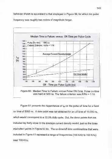
149
behavior shown is equivalent to that displayed in Figure 59, for which the pulse
frequency was roughly two orders of magnitude larger.
^50
(h)
Median Time to Failure versus Off-Time per Pulse Cycle
1600
1500
1400
1300
1200
1100
1000
900
800
700
600
500'
400
300
200-
100
Pulse On-time = 50C ns
Failuri3 Criterion: R/F to = 1.1D
oujc iwuiiciii Lyoiiaiiy iyiuuci|
On-Time Model
1 1
100 200 300 400 500 600 700 800
Off - Time per Pulse Cycle (ns)
900 1000 1100
Figure 60. Median Time to Failure versus Pulse Off-Time. Pulse on-time
was held at 500 ns. The failure criterion was R/Ro = 1.10.
Figure 61 presents the dependence of tso on the pulse off time for a fixed
on time of 5000 ns. A data point was not obtained for an off time of 10,000 ns,
which would correspond to a 33.3% duty cycle. But, the three points that are
included lay fairly close to the average current density model, just as the three
equivalent points in Figure 60 do. The on-time/off-time combinations that were
included in Figure 61 represent a range of frequencies (100 KHz to 160 KHz)
near 100 KHz.
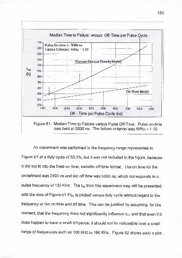
150
*50
<h)
Median Time to Failure versus Off-Time per Pulse Cycle
700
650-
600-
550
500-
150-
Pulse On-time [= 5000 ns
Failure Criterion: R/Ro = 1.10
Average Current Density Model
Model
1000 1500 2000 2500 3000 3500 4000 4500 5000 5500
Off - Time per Pulse Cycle (ns)
Figure 61 . Median Time to Failure versus Pulse Off-Time. Pulse on-time
was held at 5000 ns. The failure criterion was R/Ro = 1.10.
An experiment was performed in the frequency range represented in
Figure 61 at a duty cycle of 33.3%, but it was not included in the figure, because
it did not fit into the fixed on time, variable off time format. The on time for the
experiment was 2500 ns and the off time was 5000 ns, which corresponds to a
pulse frequency of 133 KHz. The tso from this experiment may still be presented
with the data of Figure 61 if tso is plotted versus duty cycle without regard to the
frequency or the on time and off time. This can be justified by assuming, for the
moment, that the frequency does not significantly influence tso, and that even if it
does happen to have a small influence, it should not be noticeable over a small
range of frequencies such as 100 KHz to 160 KHz. Figure 62 shows such a plot.
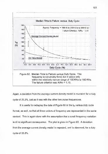
151
Median Time to Failure versus Duty Cycle
1800-
1600-j
1400-j
1200^
t 50 ioooi
(h) 800
Approx. Frequency = 100 KHz (100 KHz to 160 KHz)
Failure Criterion: R/Ro = 1.10
Average Current Density Model
(p"* rTTTTTT f -T'l'.r i n i i fn tt 'Itttt i TTTiTrTrrp T~t "r^ titttttt i p r i i| i i i i | n i i |i i i i j
30.0 35.0 40.0 45.0 50.0 55.0 60.0 65.0 70.0 75.0 80.0 85.0 90.0 95.0 100.0
Duty Cycle (%)
Figure 62. Median Time to Failure versus Duty Cycle. Thefrequency is not strictly fixed, but it varies only
within the relatively narrow range of 100 KHz to 160 KHz.
The failure criterion was R/Ro = 1.10.
Again, a deviation from the average current density model is revealed for a duty
cycle of 33.3%, just as it was with the other two pulse frequencies.
It is useful to redisplay the data of Figure 60 in the tso versus duty cycle
format, as well, so that all three orders of frequency are represented in the same
context. This is again done with the assumption that a small frequency variation
is of no significant consequence. The plot is given in Figure 63. A deviation
from the average current density model is expected, and is observed, for a duty
cycle of 33.3%.
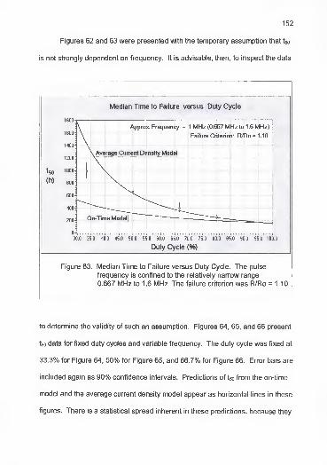
152
Figures 62 and 63 were presented with the temporary assumption that tso
is not strongly dependent on frequency. It is advisable, then, to inspect the data
*50
(h)
Median Time to Failure versus Duty Cycle
1800
1600-
400-
tpprox. Frequent7 = 1 MHz (0.667 MHz to 1.6 MHz)
\Ave
Failu re Criterio i: R/l = 1 .10
rage Current Density Modelj
1
1
\\
-
j On-Time Model
30.0 35.0 40.0 45.0 50.0 55.0 60.0 65.0 70.0 75.0 80.0 85.0 90.0 95.0 100.0
Duty Cycle (%)
Figure 63. Median Time to Failure versus Duty Cycle. The pulse
frequency is confined to the relatively narrow range
0.667 MHz to 1 .6 MHz. The failure criterion was R/Ro =1.10.
to determine the validity of such an assumption. Figures 64, 65, and 66 present
tso data for fixed duty cycles and variable frequency. The duty cycle was fixed at
33.3% for Figure 64, 50% for Figure 65, and 66.7% for Figure 66. Error bars are
included again as 90% confidence intervals. Predictions of tso from the on-time
model and the average current density model appear as horizontal lines in these
figures. There is a statistical spread inherent in these predictions, because they
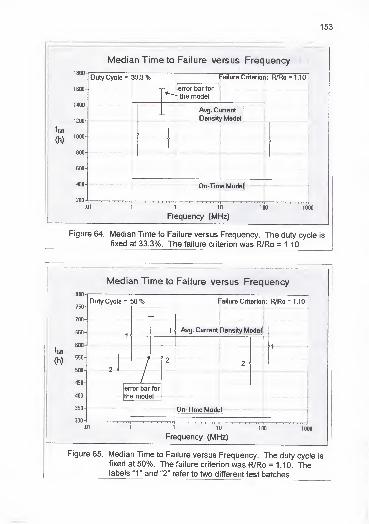
153
*50
(h)
Median Time to Failure versus Frequency
1800
1600
1400
1200
1000
800
600-
400-
200
Duty Cycle = 33.3%
01
error bar for
the model
Failure Criterion: R/Ro = 1.10
Avg. Current
Density Model
I
On-Time Model
' "I> ' I M| 1 1 1 I I I I 1 1 1 1 1 I I I | l| 1 1
|
1 1 10 100 1000
Frequency (MHz)
Figure 64. Median Time to Failure versus Frequency. The duty cycle is
fixed at 33.3%. The failure criterion was R/Ro = 1.10.
*50
(h)
Median Time to Failure versus Frequency
800
650
600
550
500
450
400
350
300
Duty Cycle = 50% frailure Criterion: R/Ro = 1.10
-
1'
1 Avg. Current Density Model
1
2 i
/
22 <
error bar for
the model
On-Time Mode l!
~1 1 r V 1 1 1TT| i • i-t -t-i-rri —i—i 1 1 1 n 1—i— 1 1 1 1
1
»- r- i i i 1 1|
Frequency (MHz)
Figure 65. Median Time to Failure versus Frequency. The duty cycle is
fixed at 50%. The failure criterion was R/Ro =1.10. Thelabels "1
" and "2" refer to two different test batches.
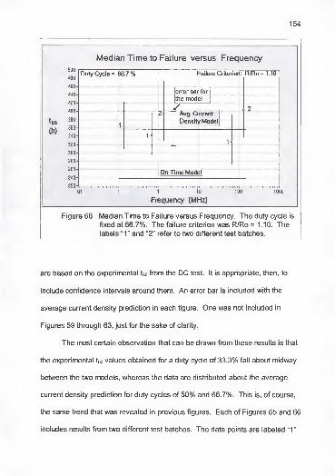
154
Median Time to Failure versus Frequency
(h)
500
480
460
440
420
400
380
360
340
320
300
280
260
240
220
01
Duty Cycle = I36.7% Failure Criterion: R/Ro = 1.10
-
• —
—
error bar for
bthe mod(;l
/ 22 Avg. Current
1,Density Model
1 <
On-Time Modei
10 100 1000
Frequency (MHz)
Figure 66. Median Time to Failure versus Frequency. The duty cycle is
fixed at 66.7%. The failure criterion was R/Ro = 1.10. Thelabels
u 1" and "2" refer to two different test batches.
are based on the experimental tso from the DC test. It is appropriate, then, to
include confidence intervals around them. An error bar is included with the
average current density prediction in each figure. One was not included in
Figures 59 through 63, just for the sake of clarity.
The most certain observation that can be drawn from these results is that
the experimental tso values obtained for a duty cycle of 33.3% fall about midway
between the two models, whereas the data are distributed about the average
current density prediction for duty cycles of 50% and 66.7%. This is, of course,
the same trend that was revealed in previous figures. Each of Figures 65 and 66
includes results from two different test batches. The data points are labeled "1"
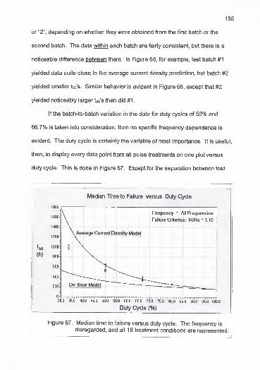
155
or "2", depending on whether they were obtained from the first batch or the
second batch. The data within each batch are fairly consistent, but there is a
noticeable difference between them. In Figure 65, for example, test batch #1
yielded data quite close to the average current density prediction, but batch #2
yielded smaller Ws. Similar behavior is evident in Figure 66, except that #2
yielded noticeably larger Ws than did #1
.
If the batch-to-batch variation in the data for duty cycles of 50% and
66.7% is taken into consideration, then no specific frequency dependence is
evident. The duty cycle is certainly the variable of most importance. It is useful,
then, to display every data point from all pulse treatments on one plot versus
duty cycle. This is done in Figure 67. Except for the separation between test
Median Time to Failure versus Duty Cycle
1800
t 50 1000i
(h) 8Q0
Frequency = All Frequencies
1 1
1
i1 1
i 1i
» » ' i i i ii
i 1 1 i i i 1 1 1 1 ii
i i i i ) i i i i i i i 1 1 | i i » i[ 1 1 i i j
30.0 35.0 40.0 45.0 50.0 55.0 60.0 65.0 70.0 75.0 80.0 85.0 90.0 95.0 100.0
Duty Cycle (%)
Figure 67. Median time to failure versus duty cycle. The frequency is
disregarded, and all 18 treatment conditions are represented.
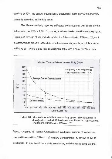
batches at 50%, the data are quite tightly clustered at each duty cycle and vary
primarily according to the duty cycle.
The lifetime analysis reported in Figures 59 through 67 was based on the
failure criterion R/Ro = 1.10. Of course, another criterion could have been used.
Figures 41 through 58 did include tso's for the failure criterion R/Ro = 1.20, so it
is worthwhile to present these data as a function of duty cycle, and this is done
in Figure 68. There is one less data point at 50%, and also at 66.7%, in this
Median Time to Failure versus Duty Cycle
2200-t
Duty Cycle (%)
Figure 68. Median time to failure versus duty cycle. The frequency is
disregarded, and all 18 treatment conditions are represented.The failure criterion was R/Ro = 1 .20.
figure, compared to Figure 67, because an insufficient number of test stripes
reached the condition R/Ro = 1 .20 to make an estimate of tso for two of the 18
treatments. In any event, the results are similar, and the conclusions are the
157
same as those connected with Figure 67. The test stripe lifetime was enhanced
significantly over the prediction of an on-time model for every pulse treatment,
enhancement was more pronounced the lower the duty cycle, and the average
current density model was a good predictor of tso for duty cycles greater than
50%. At 50%, the results from one test batch agreed well with this model, but
those of a second batch indicated less enhancement. The Ws for a duty cycle
of 33.3% were somewhat less enhanced than the average current density
prediction.
Further Discussion
It has been demonstrated that the on-time model does not provide an
accurate picture of pulsed current electromigration behavior in the range of
frequencies from 100 KHz to 133 MHz. The consistent observation of lifetime
enhancement confirms that either less damage is inflicted during each current
pulse than would be inflicted by an equal length of DC time and/or some sort of
damage recovery occurs during the time between pulses. The view of Towner
and van de Ven, and that of Brooke, as well, suggested the former. That is, they
believed that the atoms "experience" an average of the pulsed stressing current.
The findings of their work, as well as the frequent reports in the literature that the
average current density model is an accurate predictor of tso, might lend support
to this view. Other reports in the literature and the results of this work suggest,
however, that deviations from the average current density model are common.
The models of Clement, Maiz, and Dwyer predict a 1/d2dependence,
which is usually considered to be one and the same as an average current
density dependence, but they are based on idealized treatments of vacancy
supersaturation and relaxation rather than an "experienced" current concept.
These models include various simplifications, such as the assumption of a
uniform matrix or an infinite test stripe length, in order to render a tractable
treatment. There is no reason, without such simplifications, to expect a 1/d2
dependence in all practical circumstances.
The treatment given by Wu and McNutt acknowledges this fact through a
more generalized assessment. Recall that they developed the expression
t5o(pulsed) = ^)t5o(DC), (27)
where d was the duty cycle and F r was called the "damage relaxation factor."
The damage relaxation factor was defined as
Fr =1+ — • -7- 1
• (28
)Kd J
where xd was a characteristic time constant associated with the rate of damage
generation by a DC stressing current and xr was an equivalent time constant for
damage relaxation. Both xd and x r were assumed to be much larger than the on
and off times of the pulsed current. Combination of these equations gives
t50 (pulsed) d = t50 (DC) .(l-l) + t50 (DC) . (31)x
rd
The degree of lifetime enhancement is associated with the ratio Xd/xr , and Xd/xr is
probably affected by several influences, such as the local microstructure, the
local composition, current density [97], and thermal transients, to name a few.

159
With id/xr being a constant, a plot of[ t5o(pulsed) x d ] versus [ (1/d) - 1 ] should
produce a straight line according to this relation, and xjxr can be extracted from
its slope. Equation (31) expresses a 1/d2dependence when xjx r happens to be
equal to one and a 1/d dependence when Xd/xr is equal to zero.
Figure 69 is a plot of [ tso x d ] versus [ (1/d) - 1 ] for the 133 MHz results.
Each point is labeled with its corresponding duty cycle. If the data points are
340
0.0 0.2 0.4 0.6 0.8 1.0 1.2 1.4 1.6 1.8 2.0
(1/d) -
1
Figure 69. Plot of t^ x d versus (1/d) - 1 . The pulse frequency was133 MHz and the failure criterion was R/Ro =1.10.
160
assumed to reflect a continuous functional dependence, then the solid curve
may represent such a dependence. This curve has no meaning in the present
context, however, because x<j/xr is defined as a constant, and the associated
straight line must go through the DC data point. It is apparent that Figure 69
reveals at least two regimes. One of these is displayed by the data points for
duty cycles of 77%, 66.7%, and 50%, because it could be estimated that these
fall around the dashed line for a id/ir ratio equal to one. The other is associated
with the data point for 33%, which falls on the dashed line for a Xd/x r equal to 0.5.
This analysis is not meant to suggest that Equation (31) can represent
two different straight lines at the same time. The interpretation is that the 33%
point lay on a line that represents a DC-referenced xjxx of 0.5, and the other
points fall about a line that represents a DC-referenced x<j/x r of 1 . The failure of
the data to fall along a single straight line just means that some additional factor
is at work, and this factor apparently undergoes a transition somewhere between
duty cycles of 50% and 33%.
The usefulness of Figure 69 is derived from its explicit quantification of
the degree of lifetime enhancement in terms of the relative rates of damage and
recovery. For example, the data of Figure 59 indicate that tso is halfway between
the on-time prediction and the average current density prediction for a duty cycle
of 33%. In the context of Figure 69, Xd/xr= 0.5 is also halfway between these two
predictions, that is, 0.5 is halfway between zero and one.
The deviation from Xd/xr = 1 that is exhibited for a duty cycle of 33.3%
could arise from any physical influence that changes xd> xr, or both xd and x r .

161
One readily envisioned example of such an influence involves the temperature
excursions that are often associated with pulsed current stressing. When the
pulse amplitude is large enough and the pulse on times are long enough, a
significant rise in the stripe temperature may be experienced on each pulse, and
the temperature might even reach the steady state DC value. In addition, the
temperature might be allowed to drop back to that of the ambient during the off
times between pulses if they are long enough. If the amount of Joule heating is
severe, then the temperature fluctuation may be quite large. The relatively low
temperature during the off times, compared to that during the on times, would
result in a value of xjxf that is smaller than it would be if there were no
temperature fluctuations. In fact, xji, may approach zero, which is the value for
an on-time dependence of tso on duty cycle.
The experiments that were performed in this study did not involve extreme
Joule heating, and, in addition, the pulse frequencies were too high to allow any
significant temperature fluctuations. This latter contention is especially true for
the pulse frequency of 133 MHz, which is why it was chosen for Figure 69.
Some other effect was operating in these experiments.
Other possible sources of influence on Xd/xr are current density, local
microstructure, and local chemical composition, but the pulse amplitude was the
same and the samples were presumed to be identical for all pulse treatments.
There is no fundamental correlation between these factors and the pulse duty
cycle or frequency. But, a possible effective correlation between duty cycle and
microstructure was identified earlier. It was suggested that an increase in the

162
Blech length with decreasing duty cycle sometimes causes the electromigration
damage process to "select" an alternate site away from the cathode contact if the
first bamboo segment at the contact happens to be too short. So, it might be
said that the local microstructure does effectively depend on the duty cycle.
With this reasoning, it could be contended that damage occurs in bamboo
segments that are, on average, longer for small duty cycles than they are for
large duty cycles. A given accumulation of damage produces a damage gradient
that depends inversely on the segment length. Since the rate of recovery should
be proportional to the damage gradient, recovery should be slower (larger x r) for
longer segments. If so, the effective value of the ratio Xd/x r would be smaller for
small duty cycles than it is for large duty cycles, and this is just the type of
behavior displayed in Figure 69.
The possible relationship between damage location and the amount of
lifetime enhancement (or x<j/x r) can be further investigated by examining all of the
results for d = 50%. Recall that there was a noticeable spread in tso between the
two separate groups of data points that were gathered from the two different test
batches (Figure 65). The tso data for one group, batch #1 , fell about the average
current density model, but the data for the second group, batch #2, were shifted
toward less enhancement. The connection between lifetime enhancement and
damage location may be further assessed, then, independent of the duty cycle.
The histograms of Figure 70 present the normalized damage count versus
distance from the cathode for a duty cycle of 50%. These data are the same as
those that were presented in Figure 20 (d), except that they have been divided

163
(a)
(b)
(c)
6 30
I20
E 10
50% duty,
Test batch #1
i i i i i i i i r i—i—
r
012345678 9 1011121314151617181920
Distance From Cathode End (units from Fig. 20a)
50% duty,
Test batch #2
i—i—
r
i i r
2 3 4 5 6 7 8 9 1011121314151617181920
Distance From Cathode End (units from Fig. 20a)
350
13
O
Xo
batch #1
Td/tr = 1 .0
batch #2
Td/Tr = 0.7
0.0 0.5 1.0
(1/d)-
1
1.5
Figure 70. Distribution of damage versus position - 50% duty cycle.
(a) Test batch #1.
(b) Test batch #2.
(c) Estimation of id/ir for each batch.
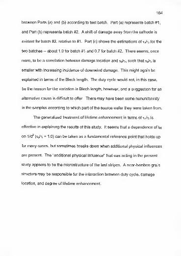
164
between Parts (a) and (b) according to test batch. Part (a) represents batch #1,
and Part (b) represents batch #2. A shift of damage away from the cathode is
evident for batch #2, relative to #1 . Part (c) shows the estimations of xjxr for the
two batches - about 1 .0 for batch #1 and 0.7 for batch #2. There seems, once
more, to be a correlation between damage location and xjxr, such that Xd/xr is
smaller with increasing incidence of downwind damage. This might again be
explained in terms of the Blech length. The duty cycle would not, in this case,
be the reason for the variation in Blech length, however, and a suggestion for an
alternative cause is difficult to offer. There may have been some nonuniformity
in the samples according to which part of the source wafer they were taken from.
The generalized treatment of lifetime enhancement in terms of xjx, is
effective in explaining the results of this study. It seems that a dependence of tso
on 1/d2
(xd/ir = 1.0) can be taken as a fundamental reference point that holds up
for many cases, but sometimes breaks down when additional physical influences
are present. The "additional physical influence" that was acting in the present
study appears to be the microstructure of the test stripes. A near-bamboo grain
structure may be responsible for the interaction between duty cycle, damage
location, and degree of lifetime enhancement.
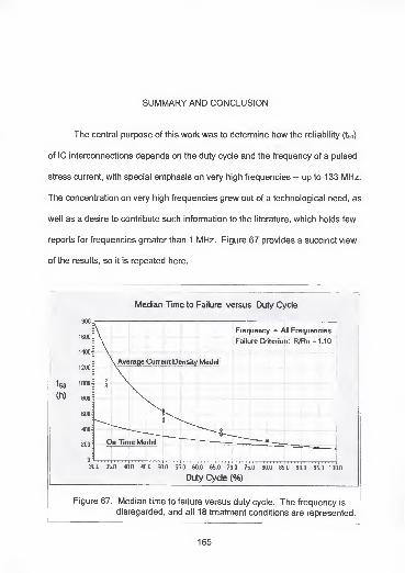
SUMMARY AND CONCLUSION
The central purpose of this work was to determine how the reliability (tso)
of IC interconnections depends on the duty cycle and the frequency of a pulsed
stress current, with special emphasis on very high frequencies - up to 133 MHz.
The concentration on very high frequencies grew out of a technological need, as
well as a desire to contribute such information to the literature, which holds few
reports for frequencies greater than 1 MHz. Figure 67 provides a succinct view
of the results, so it is repeated here.
Median Time to Failure versus Duty Cycle
1800
t 50 10001
C1) 800^
Frequency = All Frequencies
Failure Criterion: R/Ro = 1.10
30.0 35.0 40.0 45.0 50.0 55.0 60.0 65.0 70.0 75.0 80.0 85.0 90.0 95.0 100.0
Duty Cycle (%)
Figure 67. Median time to failure versus duty cycle. The frequency is
disregarded, and all 18 treatment conditions are represented.
165

166
It was found that lifetime enhancement was substantial over the entire
range of frequencies and did not depend on the frequency in any specific way.
Enhancement was more pronounced, in absolute terms, the smaller the duty
cycle, but the widely touted average current density model overestimated the
lifetime somewhat at the smallest duty cycle tested -- 33.3%. Whenever pulsed
currents are in consideration, IC miniaturization can certainly be pursued more
aggressively than an on-time prediction would allow, but care should be taken in
extending the average current density model to low duty cycles. Unique factors
related to the specific metallization scheme in question may ultimately determine
the actual behavior.
One possible "unique factor" that was identified in the present study was
the increased incidence of damage at downwind locations for small duty cycles.
By referencing the work of Frankovic et al., it was suggested that a Blech length
effect could be the cause of this behavior if it were assumed, as it often is, that a
unique Blech length is associated with each segment of a near-bamboo grain
structure. The segment over the tungsten plug contact might sometimes be too
short for any net damage to occur there, and such a condition would arise more
frequently the larger the Blech length, that is, the smaller the duty cycle. When
damage is prevented at the tungsten contact, it must "find" a longer segment
farther downwind.
A correlation was also noted between the amount of tso enhancement and
the incidence of downwind damage. This would appear, on the surface, to be a
direct reflection of the duty cycle dependence described above, but it was not

167
observed exclusively with duty cycle variations. It was also observed between
two different batches of samples tested with a duty cycle of 50%. The batch for
which tso enhancement was smaller revealed an increased incidence of damage
downwind, compared to the other, for which enhancement was larger. The
explanation was again given in terms of Blech lengths, along with the use of a
generic construct (xd/xr) from Wu and McNutt. The ratio, Xd/xr , was introduced,
where Xd/xr = 1 .0 corresponded to the average current density model and Td/xr= 0
corresponded to the on-time model. Presumably, xr increases with the length of
the bamboo segment being damaged, which is larger, on average, the larger the
Blech length. The estimated value of Xd/xr was about 0.5 for a 33.3% duty cycle
and about 1 .0 for duty cycles above 50%. At 50%, Xd/x r was about 0.7 for one
test batch (less enhancement) and about 1.0 for the other (more enhancement).
The use of a concept such as Xd/xr relies on the assumption that lifetime
enhancement is caused by a backflow of material (or vacancies) during the off
times between pulses. This is contrary to an "experienced" current view, that
has been supported by some researchers. It was seen, however, through direct
experimental observation (Figure 40), that diffusion of material may proceed
down an electromigration-induced concentration gradient at a speed comparable
to the electromigration itself.
Several models (e.g. those of Maiz, Clement, and Dwyer) predict that tso
should fundamentally be proportional to 1/d2
. This may be correct, other things
being equal, but additional influences can play a role. A microstructure-induced
Blech length effect might be the additional influence in the present work.

168
Other observations were worth noting. First, the R/Ro versus time plots
showed that the test stripe resistance often increased in discontinuous bursts
rather than one gradual rise. This was assumed to be evidence of multiple
damage sites, each requiring a different incubation period. Multiple damage
sites were indeed observed in the micrographs. Second, their was no apparent
dependence of the standard deviation of the failure times on pulse duty cycle or
frequency. The standard deviations were smaller, however, than those normally
found by other researchers.
Some of the conclusions that were offered here are a simple reflection of
the data. Others are based on additional analysis, which provided reasonable
explanations for the results, but also revealed interesting topics for future work.
The next chapter addresses this thought.

SUGGESTIONS FOR FUTURE WORK
While a number of interesting conclusions were derived from this study,
further investigations would be worthwhile. For example, there is room to
expand the range and the quantity of stress conditions tested. Such an effort
would represent a simple continuation of the path followed here. An alternate
direction could be taken as well, by pursuing other topics that are suggested by
the present findings.
It was determined that lifetime enhancement is a pervasive element of
pulsed electromigration at all high and very high frequencies up to 133 MHz.
This is an important finding, but it would be useful to push toward even higher
frequencies, possibly as high as 1 GHz. The primary obstacle would be the
difficulty of delivering a 1 GHz pulse waveform to a test stripe and faithfully
monitoring the electromigration response.
The dependence of tso on the duty cycle was not predicted well by the
average current density model at the smallest duty cycle tested - 33.3%. An
explanation was offered for this finding, but it is still necessary to investigate
smaller duty cycles, perhaps as small as 5%. Long test times would be required
to perform these experiments, however, and this may discourage such efforts.
The Blech length effect that was offered as a reason for the increased
incidence of downwind damage at small duty cycles should be confirmed with a
169

170
systematic study. Such work might involve the fabrication of special test stripes,
which have a bamboo grain structure with precisely controlled segment lengths.
First, the association of a unique Blech length with each bamboo segment could
be confirmed by determining whether the threshold current density depends on
the segment length for a constant total stripe length. The segment lengths could
then be systematically varied in an attempt to identify any possible effect on the
location of damage. The duty cycle - Blech length relationship introduced by
Frankovic et al. might also be investigated.
Any dependence of tso on the bamboo segment length could be identified
in the same setup. A decreasing tso with increasing segment length would justify
the explanation that was given for the deviations of tso from the average current
density prediction.
It would be useful to visually observe the damage process as it occurs.
The discontinuous progression of R/Ro might be more thoroughly explained from
the results. In situ chemical analysis would provide even more information,
particularly with respect to the movement of copper and its role in the behavior
of R/Ro versus time. However, such work would probably be outside the arena
of pulsed electromigration concerns, unless the pulse duty cycle or frequency
would happen to affect the mode by which R/Ro changes.
Suggestions for future work are a natural outgrowth of any research
project. They may sometimes be as important as the conclusions themselves.

APPENDIX
Test Apparatus
Summary
The purpose of this appendix is to provide specific details of the circuitry
that was constructed for this work. It is included as a documentation of circuit
schematics and to provide more detailed descriptions of circuit functions than
those provided in the main body of the dissertation. Figure 15 is presented
again, on the next page, as a guide to the major circuit functional blocks. Each
block is now discussed.
Pulse Generator
Test waveforms originate from a commercial pulse generator whose
output can be controlled with regard to frequency, duty cycle, and pulse
amplitude. It was not possible, however, to design a single distribution circuit to
accommodate the full range of test frequencies specified in this work, partly
because the gain bandwidth of a given amplifier is usually limited to some
frequency range and partly because the selection of such components as
coupling capacitors and blocking inductors depends on the frequency. As such,
the full range of frequencies which may be available from any given pulse
generator is not necessarily deliverable to the sample on any given channel.
171
172
PULSE GENERATOR
RESISTIVE POWER DIVIDER
VARIABLE ATTENUATOR
low power amp
AMPLIFIER
high power amp
dc in
rf in
TEST STRIPE FIXTUREdc voltage probe
DC OFFSET CIRCUIT COMPARATOR CIRCUIT
COMPUTER ACQUISITION
Figure 15. Flowchart depicting the essential functional blocks of
the electromigration test apparatus.
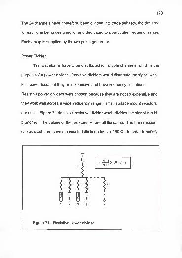
The 24 channels have, therefore, been divided into three subsets, the circuitry
for each one being designed for and dedicated to a particular frequency range.
Each group is supplied by its own pulse generator.
Power Divider
Test waveforms have to be distributed to multiple channels, which is the
purpose of a power divider. Reactive dividers would distribute the signal with
less power loss, but they are expensive and have frequency limitations.
Resistive power dividers were chosen because they are not so expensive and
they work well across a wide frequency range if small surface mount resistors
are used. Figure 71 depicts a resistive divider which divides the signal into N
branches. The values of the resistors, R, are all the same. The transmission
cables used here have a characteristic impedance of 50 Q. In order to satisfy
Figure 71 . Resistive power divider.
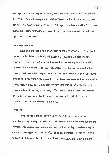
the impedance-matching requirement, then, the value of R must be chosen so
that 50 Q is "seen" looking into the divider from both directions, assuming that
the "OUT" of each branch feeds into a 50 Q input impedance and the "IN" comes
from a 50 Q output impedance. Power losses can be recovered later with the
appropriate amplifiers.
Variable Attenuator
Each channel has a voltage variable attenuator, which is used to adjust
the amplitude of the waveform on that channel, independent from the other
channels. This is needed, even in the case that the same pulse amplitude is
desired on every channel, because it is unlikely that the signals on all of the
channels will reach their respective test stripes with identical amplitudes. Each
branch will likely differ slightly from the other branches because the transmission
line lengths will not be identical and the amplifier gain will vary slightly from
branch to branch, among other things. The variable attenuator is also required,
of course, in the case that a different pulse magnitude is desired on each
channel. The circuit is shown in Figure 72.
Amplifier
Power is lost in the resistive divider and in the attenuator, so an
amplifier(s) may be required to deliver a waveform of sufficient magnitude to the
sample. Operational amplifiers, because of their versatility, would be a logical
choice for this application. A 1x10⁷A/cm
2pulse repeated at a rate of 100 MHz
with a 15% duty factor is difficult to achieve, however, with any but the most

expensive op-amps, so a wideband RF amplifier (Motorola, CA5915) was found
to handle this part of the job. The associated circuit is presented in Figure 73.
This particular amplifier has a maximum output power of 1W and a gain of
+15dB with a bandwidth up to 1200 MHz on the high end. The low end of the
Figure 72. Variable attenuator circuit.
gain bandwidth occurs at about 50 MHz, however, so a different amplifier
(Motorola, MHW591) is used from this frequency down to about 1 MHz. The
frequency range at and below 1 MHz can be handled with inexpensive
operational amplifiers (Analog Devices, AD846). It is useful in some cases to
first recover just that power which was lost in the power dividers and the
attenuators before sending the signal on to the high power amplifiers. Low
power MMIC amplifiers (Avantek, MSA -1 105) are used for this purpose, so the
"AMPLIFIER" box of Figure 15 contains this "low power amp" in addition to one
of the other three "high power amps" (CA5915, MHW591 , or AD846). Each of
the three frequency ranges just mentioned is assigned to its own dedicated
group of channels, as described earlier in the "Pulse Generator" section.
AF002N2-32
[RF IN > H( 1 RF OUT)0.1 uF

176
(a)
CA5915 or MHW591
I RF IN >-i<-nj.01 MF ^
1 2 3*56789
ormf
JYYYY. JYYY\ormf
<7 <7
.01 mF
RF OUT )
.01
< +isv pi:i
(b)
l*15V >
100
I RF IN >-*\/V^
.1uF
2 *
-15V.1pF-
1.5K
-I RF OUT >
Figure 73. Amplifier circuits.
(a) Amplifier circuit for the CA5915 and MHW591
.
(b) Operational amplifier (AD846) circuit.
(c) Low power amplifier (MSA-1 105) circuit.
DC Offset Circuit
The RF amplifier circuits and the attenuator circuits used in this system
provide an AC coupled output, that is, they do not transmit any DC component
which may have been present on the input waveform. The output is
bidirectional, so, if a unidirectional, positive current pulse is desired, for
example, then a DC offset current must be added to the output of the amplifier.
A circuit is provided for this purpose, and the schematic is given in Figure 74. It
is essentially an adjustable constant voltage source, and there is one of these
"voltage sources" for each channel. The circuit drives a DC current through a
1.5K
5K 2N22134
Figure 74. DC offset circuit.
-|/2N2219A
-TWO
series resistor, a series inductance, and into the test stripe, which are all part of
the so-called "test stripe fixture," depicted in Figure 75. The "OUT" terminal of
Figure 74 feeds into the "DC OFFSET" terminal of the test stripe fixture. It also
feeds the "dc in" line of Figure 15. More about the test stripe fixture will be
discussed shortly. The DC offset current is added to the bidirectional pulse

178
waveform coming from the amplifier ("RF in," Figs. 15 and 75), and, by changing
the sign and the magnitude of the DC current, the waveform can be shifted up or
down to produce a positive pulse train, a negative pulse train, or anything in
between.
R, L4 L3
I DC OFFSET)
yp. .01 mF
I RF IN >
(TO COMPARATOR 15.6 K
01mF
Figure 75. Test stripe fixture.
CABLE
TESTSTRIPE
Comparator Circuit
This circuit is revealed in Figure 76, and is part of the first generation
failure detection scheme. One of the inputs to the LM339A comparator is
connected to the test stripe fixture through a 5.6 KQ current-blocking resistor,
and acts to sample the DC level on the stripe, which is just equal to the offset
voltage. Since the offset voltage is produced (see the previous section) by
dividing the output of a constant voltage source between a series resistance
(resistor plus inductor) and the test stripe, the offset voltage depends on, and
changes with, the resistance of the stripe. Specifically, the offset voltage rises

179
as the stripe resistance rises. The other input to the LM339A is connected to
another adjustable voltage source. The offset voltage is "compared" to this "trip
voltage" by the comparator. The result of this comparison determines the
comparator's output voltage, which is 5 V so long as the offset voltage is less
than the trip voltage, and is zero if the offset voltage exceeds the trip voltage.
Using the fact that the offset voltage depends on the stripe resistance, the trip
voltage can be set equal to that offset voltage which corresponds to the failure
ISAMPLD-
2N2219A
Lll
F270
LED
Figure 76. Comparator circuit for failure detection.
resistance as determined from the failure criterion (a 10% increase in resistance,
for example). The pre-failure 5 V output of the comparator is used to light an

180
LED and to drive an elapsed time indicator (ETI). When the offset voltage
exceeds the trip voltage, that is, when the sample "fails," the comparator output
voltage goes to zero. The LED goes out, providing quick visual confirmation of a
failure, and the ETI stops running, thus recording the lifetime.
Computer acquisition
With the appropriate voltage measurements, a calculation of the sample
stripe resistance can be made while the stripe is under test. If these voltages
are logged periodically over the course of the test, a plot of resistance versus
time may be obtained, and this is exactly what is done with the computer-based
data acquisition (DAQ) system. A 64 channel plug-in board with DC voltage
inputs is used in conjunction with a personal computer. Under the direction of
an appropriate program, the 48 voltages which are required to calculate the
resistances of the 24 test stripes are acquired by the board at short intervals, the
resistances are calculated, and a resistance versus time file is generated. The
file can later be manipulated and plotted for display.
The determination of test stripe resistance can be made in situ while the
stripes are under test by making use of the offset circuit arrangement. The
method can be described with reference to Figure 77, which shows the test
stripe fixture together with the offset circuit. The current that goes through the
5.6 KQ resistor to the comparator circuit is negligible compared to the offset
current. Also, no DC goes through the RF coupling capacitor. It is essentially
true, then that all of the current supplied by the offset circuit goes through the
test stripe. If the total resistance of Rs, L4, L3, L2, and L1 is known (call it

181
Rseries), and if it is known that this resistance stays constant during the test (the
variability is very small, in fact), then the resistance of the test stripe, RT , can be
calculated from VT,V0 , and Rsenes- The voltages VT and V0 can, of course, be
measured with a digital voltmeter if a quick check is needed, but most data
Figure 77. DC offset circuit with the test stripe fixture.
acquisition (DAQ) is done automatically through the computer interface. The
DAQ system makes the required voltage measurements at regular time intervals,
and it automatically calculates and logs the stripe resistances at these intervals.
The calculation of stripe resistance, RT , is given by
RT -Vw
RswrieS inQ
- (32)vQ - vT
The series resistance, Rsenes, although its variation is small, is not strictly
constant. It varies slightly with the local temperature, so a simple means of
compensating for this variation was devised by calibrating the temperature

182
dependence of Rsenes for each channel to that of a reference resistance. The
DAQ program incorporates this calibration into the voltage measurements.
Test stripe fixture
The test stripe, which is akin to an integrated circuit interconnect, is
patterned onto a silicon chip by methods used in standard IC lithography and
wafer processing, the chip is mounted in a dual in-line package (DIP) and each
end of the test stripe is wired to a pin on the DIP. For testing, the DIP is plugged
into one of the specially constructed high-temperature receptacles that are
arranged on a panel inside a temperature-regulated furnace. Each receptacle
connects a DIP-packaged test stripe to the external circuitry via a 50 Q coaxial
cable. Again, the test stripe fixture was depicted in Figure 75, and it contains
the series inductors and the series resistor into which the offset circuitry is
driven, as well as the current-blocking, high-valued resistor to which the
comparator circuit is connected.
Use of the Comparator
The life status of the test stripes may be continuously indicated and the
eventual time to failure may be recorded through the comparator-based
detection scheme. This function was introduced earlier. Although the computer
DAQ system, which was added as an upgrade, makes the use of this feature
unnecessary, it can be useful when quick visual checks of the test status may be
desired during the course of a test.
183
The use of this feature goes as follows. The starting DC offset voltage VT)
and the starting stripe resistance are first determined for each test channel. It is
assumed that V0 stays constant during the test (a fairly accurate assumption),
and a calculation is made to determine that value of VT which corresponds, for
example, to a 10% increase in stripe resistance or whatever increase has been
chosen as the failure criterion. The comparator "trip" voltage is set to this value
in order to record the time of failure with the ETI. The LEDs will stay on so long
as VT is less than the trip voltage, that is, so long as the test stripes have not yet
failed.
Further Discussion of Design and Procedure
It has already been explained that this apparatus uses a constant DC
voltage, V0 , to drive the offset current to the test stripe through a series
resistance. The resulting dependence of the offset voltage, VT , on the stripe
resistance is the basis for the stripe resistance calculation. The resistance could
be monitored just as well, however, by maintaining a constant offset current,
because the DC voltage across the stripe would depend on the stripe resistance
in this case, also. The main reason for choosing the present design relates back
to the primary purpose of the offset circuit, which is to shift the AC coupled RF
pulse waveform up or down, so as to obtain a pulse train of the desired polarity.
The RF amplifiers employed here, and also the pulse generators for that matter,
have a 50 Q output impedance and therefore are intended to drive a 50 Q load.
This situation is depicted in Figure 78. V0 is the open circuit output voltage of
the amplifier, and VT is the voltage across the load.
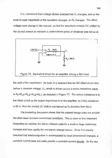
184
It is determined from voltage divider analysis that VT changes, and so the
peak-to-peak magnitude of the waveform changes, as RL changes. The offset
voltage must change in like manner, so that the waveform remains DC shifted by
the correct amount to maintain a unidirectional pulse or whatever was set up at
Figure 78. Equivalent circuit for an amplifier driving a 50Q load.
the start of the experiment. As such, it is required that the DC offset circuit also
deliver a constant voltage, V0 , which is driven across a series resistance equal
to Rs+RL4+RL3+RL2+R|_1, as depicted in Figure 77. The series resistance is to
the offset circuit as the output impedance is to the amplifier, so if this resistance
is 50 Q, then the correct DC shift is maintained as RL deviates from 50 Q.
The preceding discussion shows that the present design does not provide
the often used constant current test conditions. This is more or less important
depending on whether the failure criterion calls for a small or large resistance
increase and how rapidly the resistance change occurs. Since it is usually
assumed that electromigration is accompanied by local dimensional changes, a
constant current does not really provide a constant current density . So the use

185
of a constant current is not particularly consistent with the usual models (Black's
equation) that are employed, anyway. A constant voltage provides a constant
current density if the change in resistance is due solely to a uniform change in
the cross-section and the resistivity remains constant. It may not be fair to
assume that the local resistivity remains constant, however, and electromigration
damage does not typically show as a uniform change in cross-section. It most
often shows up as small, localized changes. When the test stripes are very long
compared to the damage area, the local changes in cross-section are much
greater than the change in resistance would indicate under the assumption that
these changes are actually taking place uniformly over the length of the test
stripe. The present setup provides something in between constant current and
constant voltage, but even so, the local current density rises severely during the
damage process. The current density in the nondamaged areas will decrease,
but this decrease is fairly small relative to the increase at the damage sites. In
the end, it is probably unimportant whether the electrical stress condition is
constant current, constant voltage, or something in between.

REFERENCES
1. Verhoeven, J., Metallurgical Reviews, 8(31), 311 (1963).
2. Huntington, H. B. in Diffusion in Solids: Recent Developments , edited by
A. S. Nowick, and J. J. Burton (Academic Press, New York, NY, 1975)
pp. 303-352.
3. Sorbello, R. S. in Electro- and Thermo-transport in Metals and Alloys ,
edited by R. E. Hummel and H. B. Huntington (AIME, New York, NY, 1977)
pp. 2-19.
4. d'Heurle, F. M. and Ho, P. S. in Thin Films: Interdiffusion and Reactions ,
edited by J. M. Poate, K. N. Tu, and J. W. Mayer (Wiley-lnterscience, NewYork, NY, 1978) pp. 243-303.
5. Kwok, T. and Ho, P. S. in Diffusion Phenomena in Thin Films andMicroelectronic Materials , edited by D. Gupta and P. S. Ho (Noyes, Park
Ridge, NJ, 1988) pp. 369-431.
6. Christou A. (editor), Electromiqration and Electronic Device Degradation
(Wiley-lnterscience, New York, NY, 1994) all pp.
7. Hummel, R. E., International Materials Reviews, 39(3), 97 (1994).
8. Huntington, H. B. and Grone, A. R., J. Phys. Chem. Solids, 20, 76 (1961).
9. Black, J. R., Proc. IEEE, 57(9), 1587 (1969).
10. Black, J. R., IEEE Trans. Electron Dev., ED-16(4), 338 (1969).
11. d'Heurle, F. M., Metallurgical Transactions, 2, 683 (1971).
12. Agarwala, B. N. in Proc. 13th Int. Reliability Physics Svmp. (IEEE, 1975)p. 107.
13. Schafft, H. A, Grant, T. C, Saxena, A. N., and Kao, C. in Proc. 23rd Int.
Reliability Physics Svmp. (IEEE, 1985) p. 93.
186
187
14. Venables, J. D. and Lye, R. G. in Proc. 10th Int. Reliability Physics Svmp.(IEEE, 1972) p. 159.
15. Sigsbee, R. A. in Proc. 11th Int. Reliability Physics Svmp. (IEEE, 1973)
p. 301.
16. Shatzkes, M. and Lloyd, J. R., J. Appl. Phys., 59(1 1), 3890 (1986).
17. Hummel, R. E., Physica Status Solidi (a), 107, K175 (1988).
18. Black, J. R. in Proc. 12th Int. Reliability Physics Svmp. (IEEE, 1974)
p. 142.
19. Hummel, R. E. and Geier, H. J., Thin Solid Films, 25, 335 (1975).
20. Blech, I. A. and Kinsbron, E., Thin Solid Films, 25, 327 (1975).
21 . Tai, K. L. and Ohring, M., J. Appl. Phys., 48, 36 (1977).
22. Gangulee, A. and d'Heurle, F. M., Scripta Met., 7, 1027 (1973).
23. Park, C. W. and Vook, R. W., Appl. Phys. Lett., 59, 175 (1991).
24. Attardo, M. J. and Rosenberg, R., J. Appl. Phys., 41, 2381 (1970).
25. Hummel, R. E., DeHoff, R. T., and Geier, H. J., J. Phys. Chem. Solids, 37,
73 (1976).
26. Spitzer, S. M. and Schwartz, S. S., IEEE Trans. Electron Dev., 16, 348(1969).
27. Blech, I. A. and Meieran, E. S., J. Appl. Phys., 40, 485 (1969).
28. Berenbaum, L., J. Appl. Phys., 42, 880 (1971).
29. Weise, J., Thin Solid Films, 13, 169 (1972).
30. Black, J. R. in Proc. 6th Int. Reliability Physics Svmp. (IEEE, 1968) p. 148.
31.
Oliver, C. B. and Bower, D.E. in Proc. 8th Int. Reliability Physics Svmp(IEEE, 1970) p. 116.
32. Learn, A. J., Appl. Phys. Lett., 19, 272 (1971).
33. Gangulee, A., J. Appl. Phys., 45, 3749 (1974).
188
34. Hummel, R. E. and Malone, D. W. in Materials Reliability Issues in
Microelectronics , edited by J. R. Lloyd, F. G. Yost, and P. S. Ho (Mater.
Res. Soc. Proc. 225, Pittsburgh, PA, 1991) p. 67.
35. Agarwala, B. N., Patnaik, B., and Schnitzel, R., J. Appl. Phys., 39, 1487
(1972).
36. Hummel, R. E. in Electro- and Thermo-transport in Metals and Alloys ,
edited by R. E. Hummel and H. B. Huntington (AIME, New York, NY, 1977)
p. 93.
37. Rosenberg, R., J. Vac. Sci. Technol., 9(1), 263 (1972).
38. Li, P., Yapsir, A. S., Rajan, K., and Lu, T-M., Appl. Phys. Lett., 54, 2443(1989).
39. Knorr, D. B., Rodbell, K. P., and Tracy, D. P. in Materials Reliability Issues
in Microelectronics , edited by J. R. Lloyd, F. G. Yost, and P. S. Ho (Mater.
Res. Soc. Proc. 225, Pittsburgh, PA, 1991) p 21.
40. Rodbell, K. P., Knorr, D. B., and Tracy, D. P. in Materials Reliability in
Microelectronics II . edited by C. V. Thompson and J. R. Lloyd (Mater. Res.
Soc. Proc. 265, Pittsburgh, PA, 1992) p. 107.
41. Knorr, D. B., Rodbell, K. P. in Materials Reliability in Microelectronics II .
edited by C. V. Thompson and J. R. Lloyd (Mater. Res. Soc. Proc. 265,Pittsburgh, PA, 1992) p. 113.
42. Vaidya, S. and Sinha, A. S., Thin Solid Films, 75, 253 (1981).
43. Nix, W. D., Metallurgical Transactions, 20A, 2217 (1989).
44. Blair, J. C, Ghate, P. B., Haywood, C. T., Appl. Phys. Lett., 17(7), 281
(1970).
45. Gangulee, A. and d'Heurle, F. M., Thin Solid Films, 16, 227 (1973).
46. Pierce, J. M. and Thomas, M. E., Appl. Phys. Lett., 39(2), 165 (1981).
47. d'Heurle, F. M. and Ames, I., Appl. Phys. Lett., 16, 80 (1970).
48. Chisholm, M. F., Aaron, D. B., Wiley, J. D., and Perepezko, J. H., Appl.Phys. Lett., 53(2), 102 (1988).
189
49. Ames, I., d'Heurle, F. M., and Horstmann, R. E., IBM J. Res. Develop. 14,
461 (1970).
50. Learn, A. J., J. Electronic Materials, 3, 531 (1974).
51. van Gurp, G. J., Appl. Phys. Lett., 19, 476 (1971).
52. Agarwala, B. N., Berenbaum, L, and Peressini, P., J. Electronic Materials,
3, 137(1974).
53. Agarwala, B. N., Digiacomo, G., and Joseph, R. R., Thin Solid Films, 34,
165 (1976).
54. Berenbaum, L. and Rosenberg, R. in Proc. 9th Int. Reliability Physics
Svmp. (IEEE. 1971) p. 136.
55. d'Heurle, F. M., Ainslie, N. G., Gangulee A., and Shine, M. C, J. Vac Sci.
Technol.,9, 289(1972).
56. d'Heurle, F. M., Gangulee, A., Aliotta, C. F., and Ranieri, V. A.,
J. Electronic Materials, 4, 497 (1975).
57. d'Heurle, F. M., Gangulee, A., Aliotta, C. F., and Ranieri, V. A.,
J. Appl. Phys., 46, 4845 (1975).
58. Agarwala, B. N., Attardo, M. J., and Ingraham, A. P., J. Appl. Phys., 41,
3954 (1970).
59. Schafft, H. A., Staton, T. C, Mandel, J., and Shott, J. D., IEEE Trans.
Electron Dev., ED-34, 673 (1987).
60. English, A. T., Tai, K. A., and Turner, P. A., J. Appl. Phys., 45, 3757(1974).
61. Scoggan, G. A., Agarwala, B. N., Peressini, P. P., and Brouillard, A. in
Proc. 13th Int. Reliability Physics Svmp. (IEEE, 1975) p. 151.
62. Kwok, T. in Proc. 26th Int. Reliability Physics Svmp. (IEEE, 1988) p. 185.
63. Kinsbron, E., Appl. Phys. Lett., 36(12), 968 (1980).
64. Iyer, S. S. and Ting, C. Y., IEEE Trans. Electron Dev., ED-31, 1468(1984).
65. Vaidya, S., Sheng, T. T., and Sinha, A. K., Appl. Phys. Lett., 36(6), 464(1980).

190
66. Ainslie, N. G., d'Heurle, F. M., and Wells, O. C, Appl. Phys. Lett., 20(4),
173(1972).
67. Blech, I. A., J. Appl. Phys., 47(4), 1203 (1976).
68. Matsuoka, F., Iwai, H., Hama, K., Itoh, H., Nakata, R., Nakakubo, T.,
Maeguchi, K., and Kanzaki, K., IEEE Trans. Electron Dev., 37, 562 (1990).
69. Tao, J., Young, K. K., Pico, C. A., Cheung, N. W., and Hu, C, IEEE Trans.
Electron Dev., 12(12), 646 (1991).
70. Hu, C.-K., Small, M. B., Rodbell, K. P., Stanis, C, Mazzeo, N., Blauner, P.,
Rosenberg, R., and Ho, P. S. in Materials Reliability in Microelectronics III
edited by K.P. Rodbell, W.F. Filter, H. J. Frost, and P. S. Ho (Mater. Res.
Soc. Proc. 309, Pittsburgh, PA, 1993) p. 111.
71. Kawasaki, H., Lee, C, and Yu, T.-K., Thin Solid Films, 253, 508 (1994).
72. Hu, C.-K., Thin Solid Films, 260, 124 (1995).
73. Shacham-Diamand, Y., MRS Bulletin, XX(1 1), 78 (1995).
74. Kim, C, Selister, S. I., Morris, Jr., J. W. in Materials Reliability in
Microelectronics III , edited by K.P. Rodbell, W.F. Filter, H. J. Frost, andP. S. Ho (Mater. Res. Soc. Proc. 309, Pittsburgh, PA, 1993) p. 127.
75. Oates, A. S. and Barr, D. L, J. Electronic Materials, 23(1), 63 (1994).
76. English, A. T., Tai, K. L., and Turner, P. A., Appl. Physics Letters, 21, 397(1972).
77. Rosenberg, R. and Ohring, M., J. Appl. Phys., 42(13), 5671 (1971).
78. Blech, I. A. and Herring, C, Appl. Phys. Lett., 29(3), 131 (1976).
79. Davis, J. R., Proc. IEE, 123(11), 1209 (1976).
80. Miller, R. J. in Proc. 16th Int. Reliability Physics Svmp. (IEEE, 1978)p. 241.
81. Kinsbron, E., Melliar-Smith, C. M., and English, A. T., IEEE Trans.Electron Dev., ED-26(1), 22 (1979).
82. Schoen, J. M., J. Appl. Physics, 51(1), 508 (1980).

191
83. Arzigian, J. S. in Proc. 21st Int. Reliability Physics Svmp. (IEEE, 1983)
p. 32.
84. Wu, C. J. and McNutt, M. J. in Proc. 21st Int. Reliability Physics Svmp.(IEEE, 1983) p. 24.
85. English, A. T. and Kinsbron, E., J. Appl. Phys., 54(1), 275 (1983).
86. Towner, J. M. and van de Ven, E. P. in Proc. 21st Int. Reliability Physics
Svmp. (IEEE. 1983) p. 36.
87. Brooke, L. in Proc. 25th Int. Reliability Physics Svmp. (IEEE, 1987) p. 136.
88. Lloyd, J. R. and Koch, R. H. in Proc. 25th Int. Reliability Physics Svmp.(IEEE, 1987) p. 161.
89. Lloyd, J. R. and Koch, R. H., Appl. Phys. Lett. 52(3), 194 (1988).
90. Harrison, J. W., IEEE Trans. Electron Dev., 35(12), 2170 (1988).
91 . Suehle, J. S. and Schafft, H. A. in Proc. 27th Int. Reliability Physics Svmp.(IEEE, 1989) p. 229.
92. Liew, B. K., Cheung, N. W., and Hu, C. in Proc. 27th Int. Reliability
Physics Svmp. (IEEE, 1989) p. 215.
93. Maiz, J. A. in Proc. 27th Int. Reliability Physics Svmp. (IEEE, 1989) p. 220.
94. Hatanaka, K., Noguchi, T., and Maeguchi, K. in Symposium on VLSITechnology: Digest of Technical Papers (IEEE and JSAP, 1989) p. 19.
95. Hummel, R. E. and Hoang, H. H., J. Appl. Physics, 65(5), 1929 (1989).
96. Liew, B. K., Cheung, N. W., and Hu, C, IEEE Trans. Electron Dev. 37(5),1343 (1990).
97. Suehle, J. S. and Schafft, H. A. in Proc. 28th Int. Reliability Physics Svmp(IEEE, 1990) p. 106.
98. Liew, B. K., Fang, P., Cheung, N. W., and Hu, C. in Proc. 28th Int.
Reliability Physics Svmp. (IEEE, 1990) p. 111.
99. Tao, J., Young, K. K., Pico, C. A., Cheung, N. W., and Hu, C, IEEEElectron Dev. Lett., 12(12), 646 (1991).

192
100. Kwok, T., Kaufman, R., and Davari, B. in Materials Reliability Issues in
Microelectronics , edited by J. R. Lloyd, F. G. Yost, and P. S. Ho (Mater.
Res. Soc. Proc. 225, Pittsburgh, PA, 1991) pp. 85-89.
101. Clement, J. J., J. Appl. Phys. 71(9), 4264 (1992).
102. Clement, J. J. in Materials Reliability in Microelectronics II . edited by C. V.
Thompson and J. R. Lloyd (Mater. Res. Soc. Proc. 265, Pittsburgh, PA,
1992) pp. 57-63.
103. Tao, J., Young, K., Cheung, N., and Hu, C. in Proc. 30th Int. Reliability
Physics Svmp. (IEEE, 1992) p. 338.
104. Li, Z., Bauer, C. L., Mahajan, S, and Milnes, A. G., J. Appl. Phys., 72(5),
1821 (1992).
105. Hinode, K., Furusawa, T., and Homma, Y. in Proc. 30th Int. Reliability
Physics Svmp. (IEEE, 1992) p. 205.
106. Castano, E. and Maiz, J., Microelectron. and Reliab., 33(8), 1189 (1993).
107. Baldini, G. L., Scorzoni, A., and Tamarri, F., Microelectron. and Reliab.,
33(11/12), 1841 (1993).
108. Ting, L. M., May, J. S., Hunter, W. R., and McPherson, J. W. in Proc. 31st
Int. Reliability Physics Svmp. (IEEE, 1 993) p. 31 1
.
109. Tao, J., Cheung, N., and Hu, C, IEEE Trans. Electron Dev., 41(4), 539(1994).
110. Pierce, D. G., Snyder, E. S., Swanson, S. E., and Irwin, L. W. in Proc.
32nd Int. Reliability Physics Svmp. (IEEE, 1994) p. 198.
111. Ohfuji, S. and Tsukada, M., J. Appl. Phys, 78(6), 3769 (1995).
112. Frankovic, R., Bernstein, G. H., and Clement, J. J. in Materials Reliability
in Microelectronics VI . edited by W. F. Filter, J. J. Clement, A. S. Oates,R. Rosenberg, and P. M. Lenahan (Mater. Res. Soc. Proc. 428,Pittsburgh, PA, 1996) p. 109.
113. Frankovic, R., Bernstein, G. H., and Clement, J. J., IEEE Electron DevLett., 17(5), 244(1996).

193
1 14. Verbruggen, A. H., van den Homberg, M. J. C, Kalkman, A. J.,
Kraayeveld, J. R., Willemsen, A. W.-J., and Radelaar, S. in Materials
Reliability in Microelectronics VI , edited by W. F. Filter, J. J. Clement, A.
S. Oates, R. Rosenberg, and P. M. Lenahan (Mater. Res. Soc. Proc. 428,Pittsburgh, PA, 1996) p. 121.
115. Tao J., Chen, J. F., Cheung, N. W., and Hu, C, IEEE Trans. Electron
Dev., 43(5), 800(1996).
1 16. Tao J., Chen, J. F., Cheung, N. W., and Hu, C. in Proc. 34th Int. Reliability
Physics Svmp. (IEEE, 1996) p. 180.
117. Dwyer, V. M., IEEE Trans. Electron Dev., 43(6), 877 (1996).
BIOGRAPHICAL SKETCH
David Wayne Malone was born on May 30, 1962, in Cincinnati, Ohio, and
was raised in Melbourne, Florida. He attended Melbourne High School from
1977 to 1980, and upon graduation, he pursued further education in the field of
engineering. While in attendance at the University of Florida, David obtained
practical experience with Occidental Chemical Company, White Springs, FL, and
Harris Corporation, Melbourne, FL, through the Cooperative Education program.
He received his bachelor's degree in materials science and engineering from the
University of Florida in May of 1987. David returned to the University of Florida
in 1988 to pursue graduate studies and to perform research under the
supervision of Professor Rolf E. Hummel. He investigated novel techniques of
thin film deposition, as well as pulsed current electromigration. He received his
master's degree in May of 1992 and his doctoral degree in May of 1997.
194

I certify that I have read this study and that in my opinion it conforms to
acceptable standards of scholarly presentation and is fully adequate, in scopeand quality, as a dissertation for the degree of Doctor of Philosophy.
Rolf E. Hummel, Chairman
Professor of Materials Science
and Engineering
I certify that I have read this study and that in my opinion it conforms to
acceptable standards of scholarly presentation and is fully adequate, in scopeand quality, as a dissertation for the degree of Doctor of Philosophy.
Robert T. DeHoff
Professor of Materials Science
and Engineering
I certify that I have read this study and that in my opinion it conforms to
acceptable standards of scholarly presentation and is fully adequate, in scopeand quality, as a dissertation for the degree of Doctor of Philosophy.
Robert M. Park
Professor of Materials Science
and Engineering
I certify that I have read this study and that in my opinion it conforms to
acceptable standards of scholarly presentation and is fully adequate, in scopeand quality, as a dissertation for the degree of Doctor of Philosophy.
Rajiv K. Singh
Associate Professor of Materials
Science and Engineering

I certify that I have read this study and that in my opinion it conforms to
acceptable standards of scholarly presentation and is fully adequate, in scope
and quality, as a dissertation for the degree of Doctor of Philosophy.
Timothy ^. Anderson
Professor of Chemical
Engineering
This dissertation was submitted to the Graduate Faculty of the College of
Engineering and to the Graduate School and was accepted as partial fulfillment
of the requirements for the degree of Doctor of Philosophy.
May, 1997
Winfred M. Phillips
Dean, College of Engineering
Karen A. Holbrook
Dean, Graduate School


