Metal Width Variation (Type 1 and Type 2) _VLSI Concepts
5
5/ 24/2016 Metal Wi dt h V ariation (Type 1 and Type 2) |VLSI Concepts ht tp: //www.vl si-expert.com/2015/10/met al -wi dth-vari at i on-type- 1-and-t ype-2.ht ml 1/ 5 A online information Center for all who have Interest in Semiconductor Industry. VLSI Concepts Select Langu age Powered Translate page Max Life Term Plan 1 Cr Lumpsum + Rs 40000 Monthly Income @ Just Rs. 22/day*. Buy Now! Search Search This Blog Sunday, October 4, 2015 Metal Width Variation (Type 1 and Type 2) In the previous articles, we have discussed a lot about the Etching, CMP, Lithography and their effects. Now it’s the time to know 1. How these variations are modeled in real? 2. How foundry provide the corresponding data? 3. How to read that one and provide the info to different tools? Let’s start with the Summary figures of last post. Note: Blue is what we need ideally and brown is what we will get actually/practically. As we have disc ussed in last few post that t here are basically 3 parameters w hich are affected a lot. Width of metal Thickness of Dielectric and Thickness of Metal. Metal Width Variation (Part 1) CONT ACT ME (vlsi.exper t@gmail. co RELATED POST Job Opportunity Points to Remember for Preparing a Relat ed Art icles: 5 Steps to Build Ca VLSI Industry Reluctant to Hire ... Featured Post How to Prepare Good Resum Follow by Email Email address... Be the first of your friends to like Vlsi expert 4.2k li Like Page VLSI EXPERT (vlsi EG) google.com/+Vlsi-expert Bridging Gap Between Acdamia and Industry 103 followers Follow 1 More Next Blog»
-
Upload
sumanth-varma -
Category
Documents
-
view
216 -
download
0
Transcript of Metal Width Variation (Type 1 and Type 2) _VLSI Concepts
7/26/2019 Metal Width Variation (Type 1 and Type 2) _VLSI Concepts
http://slidepdf.com/reader/full/metal-width-variation-type-1-and-type-2-vlsi-concepts 1/5
5/24/2016 Metal Width Variation (Type 1 and Type 2) |VLSI Concepts
http://www.vlsi-expert.com/2015/10/metal-width-variation-type-1-and-type-2.html
A online information Center for all who have Interest in Semiconductor Industry.
VLSI Concepts Select Language Pow
Translate page
Max Life Term Plan1 Cr Lumpsum + Rs 40000 Monthly Income @ Just Rs. 22/day*. Buy Now!
Search
Search This Blog
Sunday, October 4, 2015
Metal Width Variation (Type 1 and Type 2)
In the previous articles, we have discussed a lot about the Etching, CMP, Lithography and their effects. Now it’s the time to know
1. How these variations are modeled in real?
2. How foundry provide the corresponding data?
3. How to read that one and provide the info to different tools?
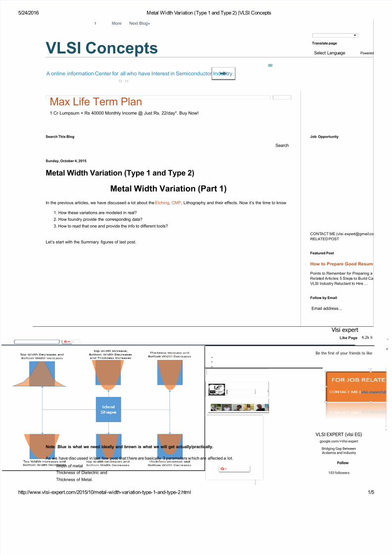
Let’s start with the Summary figures of last post.
Note: Blue is what we need ideally and brown is what we will get actually/practically.
As we have disc ussed in last few post that t here are basically 3 parameters w hich are affected a lot.
Width of metal
Thickness of Dielectric and
Thickness of Metal.
Metal Width Variation (Part 1)
CONTACT ME (vlsi.expert@gma
RELATED POST
Job Opportunity
Points to Remember for Preparin
Related Articles: 5 Steps to Build
VLSI Industry Reluctant to Hire ..
Featured Post
How to Prepare Good Res
Follow by Email
Email address...
Be the first of your friends to
Vlsi expert4.2Like Page
VLSI EXPERT (vlsi EG)
google.com/+Vlsi-expert
Bridging Gap BetweenAcdamia and Industry
103 followers
Follow
1 More Next Blog»

7/26/2019 Metal Width Variation (Type 1 and Type 2) _VLSI Concepts
http://slidepdf.com/reader/full/metal-width-variation-type-1-and-type-2-vlsi-concepts 2/5
5/24/2016 Metal Width Variation (Type 1 and Type 2) |VLSI Concepts
http://www.vlsi-expert.com/2015/10/metal-width-variation-type-1-and-type-2.html
From the above figure and also from statement, you can easily conclude that there are 2 mainly type of variation – In width and In
height. Let’s start one by one.
There are different ways to model variation information of this parameter. Different EDA vendors code this info in different way (I will
summarize this in the last of this Article series). Similarly, Foundries also provide this info in different way.
Most common and simpler form of variation is “variation in percentage” or “absolute numbers” in the form of table.
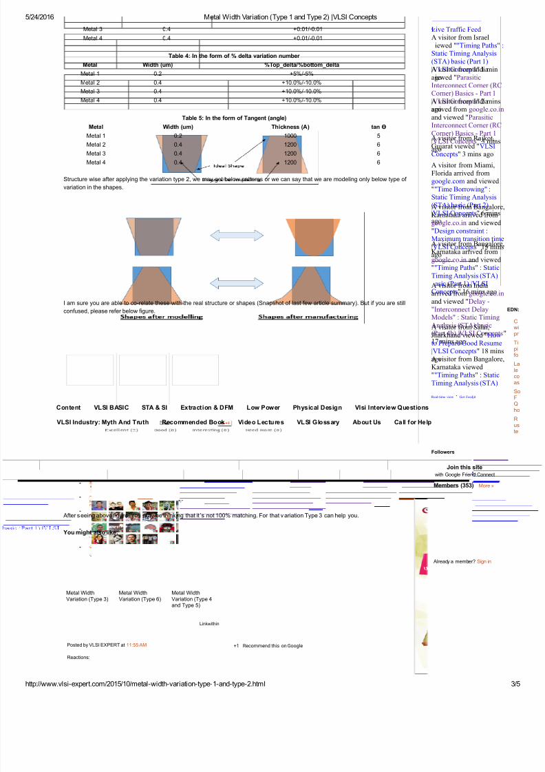
Table 1: In the form of variation %
Metal Width (um) variation in % (+/-)Metal 1 0.02 8
Metal 2 0.04 8
Metal 3 0.04 9
Metal 4 0.04 10
Structure wise after applying the variation type 1, we may get below patterns or we can say that we are modeling only below type of
variation in the shapes.
In this type of variation, we assume that width variation is same from top to bottom OR if there is any difference, their effect in
Capacitance and Resistance are negligible. I have just used 2 words, CAPACITANCE and RESISTANCE, so it’s my moral duty to
ask this question- “How, above type of width variation impact the CAP and RES of the Circuit?” :)
I would say – think and if you forget then please refer Parasitic Interconnect Corner article. It will help you to refresh your concept
And don’t worry I will also s ummarize this later on.
In this we will remove the restriction of Type 1 (same bottom and top width variation). It’s now more closure toward the practical
shape. And foundry consider this for 180nm and below nodes.
Ideal Width of Metal = W (Rectangle shape)
Because of several fabrication steps (already discussed in last few Articles of this series), final shape of the Metal is not
rectangular. It’s trapezoidal, so we have to define 2 widths.
Top_width = W+2A
Bottom_Width = W-2A
Note:
Here we are considering that “bottom delta” = “top delta”.
In case, top_width_delta=bottom_width_delta, we can model this by using the angle Ɵ also. Where tan Ɵ = 2B/2A
and known as Tangent.
So, in all the above case the table (or say info provided by Foundry) can be any of the following.
Table 2: In the form of absolute Numbers (final width)
Metal Width (um) Top_width/bottom_width
Metal 1 0.2 0.21/0.19
Metal 2 0.4 0.41/0.39
Metal 3 0.4 0.41/0.39
Metal 4 0.4 0.41/0.39
Table 3: In the form of absolute variation number
Metal Width (um) Top_delta/bottom_delta
Metal 1 0.2 +0.01/-0.01
Metal 2 0.4 +0.01/-0.01
Width Of Metal:
Width Variation Type 1:
Width Variation Type 2:
3,296,803
Total Pageviews
Subscribe To VLSI EXPERT
Posts
Comments
Basic of Timing Analysis in Physi calDesign
"Timing Paths" : StaticTiming Analysis (STA)basic (Part 1)
Delay - "Wire LoadModel" : Static Timing
Analysis (STA) basi c(Part 4c)
Delay - "InterconnectDelay Models" : StaticTiming Analysis (STA)basic (Part 4b)
"Setup and Hold Time": Static Timing Analysis(STA) basic (Part 3a)
"Setup and Hold TimeViolation" : StaticTiming Analysis (STA)basic (Part 3b)
"Examples Of Setupand Hold time" : StaticTiming Analysis (STA)basic (Part 3c)
"Time Borrowing" :Static Timing Analysis(STA) basic (Part 2)
Effect of Wire LengthOn the Slew: Static
Timing Analysis (STA)Basic (Part-7a)
Effect of Thresholdvoltage: Static Timing
Analysis (STA) Basic(Part-7c)
Popular Posts
Recent Visitors
►
▼
►
►
►
►
►
►
B
7/26/2019 Metal Width Variation (Type 1 and Type 2) _VLSI Concepts
http://slidepdf.com/reader/full/metal-width-variation-type-1-and-type-2-vlsi-concepts 3/5
5/24/2016 Metal Width Variation (Type 1 and Type 2) |VLSI Concepts
http://www.vlsi-expert.com/2015/10/metal-width-variation-type-1-and-type-2.html
Posted by VLSI EXPERT at 11:55 AM
Reactions:
Metal WidthVariation (Type 3)
Metal WidthVariation (Type 6)
Metal WidthVariation (Type 4and Type 5)
Metal 3 0.4 +0.01/-0.01
Metal 4 0.4 +0.01/-0.01
Table 4: In the form of % delta variation number
Metal Width (um) %Top_delta/%bottom_delta
Metal 1 0.2 +5%/-5%
Metal 2 0.4 +10.0%/-10.0%
Metal 3 0.4 +10.0%/-10.0%
Metal 4 0.4 +10.0%/-10.0%
Table 5: In the form of Tangent (angle)
Metal Width (um) Thickness (A) tan Ɵ
Metal 1 0.2 1000 5
Metal 2 0.4 1200 6
Metal 3 0.4 1200 6
Metal 4 0.4 1200 6
Structure wise after applying the variation type 2, we may get below patterns or we can say that we are modeling only below type of
variation in the shapes.
I am sure you are able to co-relate these with the real structure or shapes (Snapshot of last few article summary). But if you are still
confused, please refer below figure.
After s eeing above figure, you may be thinking that it ’s not 100% matching. For that v ariation Type 3 can help you.
You might also like:
Linkwithin
+1 Recommend this on Google
Live Traffic Feed
Real-time view · Get Feedjit
A visitor from Israeliewed ""Timing Paths" :
Static Timing Analysis(STA) basic (Part 1)|VLSI Concepts" 1 minagoA visitor fr om India
iewed "ParasiticInterconnect Corner (RCCorner) Basics - Par t 1|VLSI Concepts" 2 minsagoA visitor fr om Indiaarrived from google.co.inand viewed "ParasiticInterconnect Corner (RC
Corner) Basics - Part 1|VLSI Concepts" 3 minsago
A visitor from Ra jkot,Gujarat viewed "VLSIConcepts" 3 mins ago
A visitor from Miami,Florida arrived fromgoogle.com and viewed""Time Borrowing" :Static Timing Analysis(STA) basic (Part 2)|VLSI Concepts" 6 minsago
A visitor from Bangalore,Karnataka arrived fromgoogle.co.in and viewed"Design constraint :Maximum transition time|VLSI Concepts" 15 minsago
A visitor from Bangalore,Karnataka arrived fromgoogle.co.in and viewed
""Timing Paths" : StaticTiming Analysis (STA)asic (Part 1) |VLSI
Concepts" 16 mins agoA visitor from Indiaarrived from google.co.inand viewed "Delay -"Interconnect DelayModels" : Static TimingAnalysis (STA) basic(Part 4b) |VLSI Concepts"17 mins ago
A visitor from Salai,Jharkhand viewed "Howto Prepare Good Resume|VLSI Concepts" 18 minsagoA visitor from Bangalore,Karnataka viewed""Timing Paths" : StaticTiming Analysis (STA)
E
Join this site
with Google Friend Connect
Members (353) More »
Already a member? Sign in
Followers
Content VLSI BASIC STA & SI Extraction & DFM Low Power Physical Design Vlsi Interview Questions
VLSI Industry: Myth And Truth Recommended Bo ok Vi de o L ec tu re s VL SI G lo ss ary Ab ou t Us Ca ll for He lp
7/26/2019 Metal Width Variation (Type 1 and Type 2) _VLSI Concepts
http://slidepdf.com/reader/full/metal-width-variation-type-1-and-type-2-vlsi-concepts 4/5
5/24/2016 Metal Width Variation (Type 1 and Type 2) |VLSI Concepts
http://www.vlsi-expert.com/2015/10/metal-width-variation-type-1-and-type-2.html
Newer Post Older PostHome
Subscribe to: Post Comments (Atom)
Enter your comment...
Comment as: Google Accou
Publish
Preview
Create a Link
No comments:
Post a Comment
Links to this post
Must Read Articles
Design constraint :
Maximum transitio...
www.vlsi-expert.com
Clock
Reconvergence P...
www.vlsi-expert.com
Effect of Wire
Length On the Sle...
www.vlsi-expert.com
10 Ways to fix
SETUP and HOLD...
www.vlsi-expert.com
"Setup and Hold
Time Violation" : S...
www.vlsi-expert.com

7/26/2019 Metal Width Variation (Type 1 and Type 2) _VLSI Concepts
http://slidepdf.com/reader/full/metal-width-variation-type-1-and-type-2-vlsi-concepts 5/5
5/24/2016 Metal Width Variation (Type 1 and Type 2) |VLSI Concepts
http://www.vlsi-expert.com/2015/10/metal-width-variation-type-1-and-type-2.html
Add This
Synopsys Design
Constraints (SDC)...
www.vlsi-expert.com
"Examples Of Setup
and Hold time" : St...
www.vlsi-expert.com
"Delay - Timing path
Delay" : Static Timi...
www.vlsi-expert.com
Delay - "Wire Load
Model" : Static Tim...
www.vlsi-expert.com
Why VLSI Industry
Reluctant to Hire F...
www.vlsi-expert.com
Vlsi expert group. Simple template. Powered by Blogger .