Metal “Gate” Insulator Semiconductor - users-new.ece...
63
ECE 3040 - Dr. Alan Doolittle Georgia Tech MOS Capacitor Metal “Gate” Insulator Semiconductor “MOS” = Metal- Oxide- Semiconductor “MOS” actually refers to “Metal”– Silicon Dioxide – Silicon Other material systems have similar “MIS” structures formed by Metal – Insulator – Semiconductor The capacitor itself forms the basis of digital logic circuits, and DRAM storage units (storing charge) or can simply supply a capacitance for an analog integrated circuit. It will also be the building block for the most common transistor produced – the MOS transistor. The substrate is normally taken to be grounded and the “Gate” electrode can be biased with a voltage, V G
Transcript of Metal “Gate” Insulator Semiconductor - users-new.ece...
ECE 3040 - Dr. Alan DoolittleGeorgia Tech
MOS Capacitor
Metal “Gate”Insulator
Semiconductor
“MOS” = Metal- Oxide- Semiconductor
“MOS” actually refers to “Metal”– Silicon Dioxide – Silicon
Other material systems have similar “MIS” structures formed by Metal –Insulator – Semiconductor
The capacitor itself forms the basis of digital logic circuits, and DRAM storage units (storing charge) or can simply supply a capacitance for an analog integrated circuit. It will also be the building block for the most common transistor produced – the MOS transistor.
The substrate is normally taken to be grounded and the “Gate” electrode can be biased with a voltage, VG

ECE 3040 - Dr. Alan DoolittleGeorgia Tech
Key assumptions:1) Metal is an equipotential region.2) Oxide is a perfect insulator with zero current flow.3) Neither oxide nor oxide-semiconductor interface have charge centers.4) Semiconductor is uniformly doped.5) An ohmic contact has been established on the back side of thewafer.6) Analysis will be one-dimensional.7) The semiconductor is thick enough to have a quasi-neutral region (where electric field is zero and all energy bands are flat).8) Certain energy relationships exist:
ΦM = ΦS = χ + (EC - EF )FB (terms defined in next few slides)
MOS Capacitor

ECE 3040 - Dr. Alan DoolittleGeorgia Tech
MOS Capacitor
EO= Vacuum Energy Level. The minimum energy an electron must have to free itself from the material.
ΦM = “Work function” of the metal. This is the energy difference from the fermi energy (average energy) of an electron in the metal to the vacuum energy level.
ΦS = “Work function” of the semiconductor. This is the energy difference from the fermi energy (average energy) of an electron in the semiconductor to the vacuum energy level. Note that this energy depends on doping since EF depends on doping
χ = Electron Affinity of the semiconductor. This is the energy difference from the conduction band minimum in the semiconductor to the vacuum energy level. Note that this energy does NOT depend on doping
(EC - EF )FB= ΦS – χ in the quasi-neutral region where the bands are not bent or are in “flat band”

ECE 3040 - Dr. Alan DoolittleGeorgia Tech
The insulator is simply a very wide bandgap, intrinsically doped semiconductor characterized by an electron affinity, χi .
The semiconductor can have an electric field near the insulator that forces the energy bands to bend near the insulator-semiconductor interface.
MOS Capacitor

ECE 3040 - Dr. Alan DoolittleGeorgia Tech
MOS Capacitor
Since the insulator prevents any current from flowing, when we bring the materials together, the fermi-energy must be flat.
Likewise, if no charges are stored on the “plates” (metal and semiconductor regions near the insulator) of the capacitor, the bands are not bent in the insulator nor semiconductor. Note the assumption of an equipotential surface in the metal simply states that a perfect conductor can not support and electric field (electrostatics).
ECE 3040 - Dr. Alan DoolittleGeorgia Tech
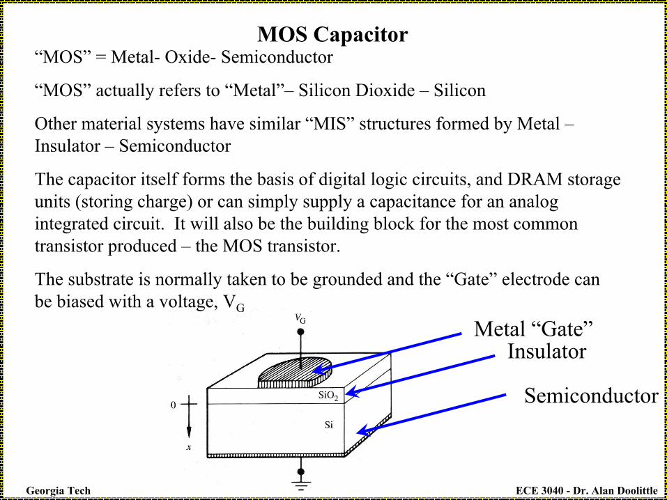
MOS CapacitorCapacitor under bias
A positive voltage on the gate puts positive charge on the gate electrode. Gauss’s law forces an equal negative charge to form near the semiconductor-insulator interface.
Charge separated by a distance implies an electric field across the insulator.

ECE 3040 - Dr. Alan DoolittleGeorgia Tech
If VG = bias voltage applied to the gate (metal).
For all VG the Fermi level in the each layer remains flat due to zero current through the structure.
The applied bias separates the Fermi levels at the metal and semiconductor ends by qVG
EF(metal) - EF(semiconductor) = -qVG
If the semiconductor is grounded (fixed at any constant potential we can call ground):
•metal side Fermi level moves downward if VG > 0
•metal side Fermi level moves upward if VG < 0
Applying Poisson’s equation to the oxide, since there are no charges in the oxide,
bandsenergy thedoes so ith x,linearly w variespotential theSince
ith xlinearly w varies
tan0
PotentialdxEV
tConsEdx
dE
oxide
oxideoxide
⇒=
=⇒==
∫
ρ
MOS CapacitorCapacitor under bias

ECE 3040 - Dr. Alan DoolittleGeorgia Tech
MOS CapacitorCapacitor under bias
For an n-type semiconductor.•When VG > 0 the metal fermi-energy is lowered (E=-qV), the insulator has an electric field across it that terminates almost immediately in the near perfectly conducting metal, but terminates over a finite distance in the semiconductor of “finite resistivity”.•The charge model indicates that negative charge must be created in the semiconductor near the interface. This charge is in the form of electrons.•Since n = niexp[(EF - Ei)/ kT], the electron concentration in the semiconductor near interface increases.•This is called accumulation

ECE 3040 - Dr. Alan DoolittleGeorgia Tech
MOS CapacitorCapacitor under bias
For an n-type semiconductor.•When VG < 0 the metal fermi-energy is raised (E=-qV), the insulator has an electric field across it that terminates almost immediately in the near perfectly conducting metal, but terminates over a finite distance in the semiconductor of “finite resistivity”.•The charge model indicates that positive charge must be created in the semiconductor near the interface. This charge is in the form of ionized donors.•Since n = niexp[(EF - Ei)/ kT], the electron concentration in the semiconductor near interface decreases.•This is called depletion.

ECE 3040 - Dr. Alan DoolittleGeorgia Tech
MOS CapacitorCapacitor under bias
For an n-type semiconductor.•For higher magnitudes of bias (VG < 0) the fermi-energy near the interface crosses-the intrinsic energy and the “type” of material swaps from n-type to p-type (only locally near the interface).•The charge model indicates that positive charge must be created in the semiconductor near the interface. This charge is in the form of ionized donors and holes.
Inversion continued on next slide…

ECE 3040 - Dr. Alan DoolittleGeorgia Tech
MOS CapacitorCapacitor under bias
Inversion Continued…•The hole concentration near the interface must equal the donor concentration. Thus,
pinterface = NDpinterface = niexp[(Ei-INTERFACE -EF)/ kT] = niexp[(EF – Ei-BULK)/ kT]
•This is called inversion.•The onset of inversion occurs for a voltage called the threshold voltage VT (not thermal voltage)•Detailed calculations taking into account the charge distribution as a function of position in the semiconductor indicates that inversion occurs when,
Ei-INTERFACE - Ei-BULK = 2 (EF - Ei-BULK)

ECE 3040 - Dr. Alan DoolittleGeorgia Tech
MOS CapacitorCapacitor under bias
For an n-type semiconductor.•For still higher magnitudes of bias (VG < 0) the hole concentration continues to increase resulting in a very high concentration of holes near the interface.•This is known as strong inversion.
Strong Inversion(VG < VT)

ECE 3040 - Dr. Alan DoolittleGeorgia Tech
MOS CapacitorCapacitor under bias for P-type material
ECE 3040 - Dr. Alan DoolittleGeorgia Tech
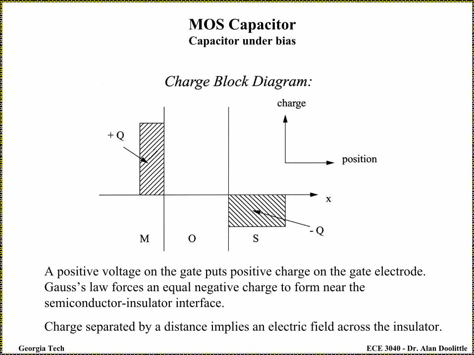
MOS CapacitorCapacitor under bias Summary
Inversion Depletion Accumulation
VT 0VG
InversionDepletionAccumulation
VT0VG
N-type material
P-type material

ECE 3040 - Dr. Alan DoolittleGeorgia Tech
Let φ(x) = electrostatic potential inside the semiconductor at a depth x (measured from the oxide interface)
( ) ( )[ ]
[ ]
[ ]FBULKiF
INTERFACEiBULKiS
iBULKi
EEq
withalong
potentialsurfaceEEq
xEEq
x
−=
≡−=
≡−=
−
−−
−
1,
1and
potential ticelectrosta 1
φ
φ
φ
MOS CapacitorQuantitative Solution
P-type Example
ECE 3040 - Dr. Alan DoolittleGeorgia Tech
MOS CapacitorQuantitative Solution
( ) ( )
TG
BULKBULK
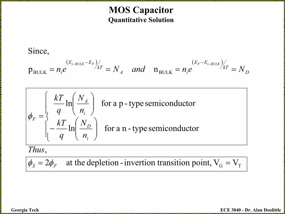
VV point, transitioninvertion -depletion at the2,
torsemiconduc type-n afor ln
torsemiconduc type-p afor ln
np
Since,
==
−
=
====−− −−
FS
i
D
i
A
F
DkT
EE
iAkT
EE
i
Thus
nN
qkT
nN
qkT
NenandNenBULKiFFBULKi
φφ
φ

ECE 3040 - Dr. Alan DoolittleGeorgia Tech
MOS CapacitorQuantitative Solution
Since the MOS-Capacitor is symmetric (equal charge on metal as is in the semiconductor) and has no charge in the oxide, we can solve for the electrostatic variables using only the semiconductor section of material.
Things to note:
Charge due to accumulation bias and inversion bias results in a very narrow charge distribution near the interface.
Charge due to depletion bias results in a wide “depletion width”, W

ECE 3040 - Dr. Alan DoolittleGeorgia Tech
MOS CapacitorQuantitative Solution
Once again, if we apply the “Depletion Region Approximation” (neglect all charges but those due to ionized dopants) and assume p-type material,
( ) widthdepletion theis W whereW)x(0for ≤≤−≅−+−= AAD qNNNnpqρ
And from Poisson’s equation using a boundary condition that the electric field goes to zero at the depletion region edge,
( )xWKqN
dxdxE
KqN
dxdE
oS
A
oS
A −=−=⇒−
=ε
φε
)(
And finally, the electrostatic potential can be found by integrating using a boundary condition that the electrostatic potential goes to zero at the depletion region edge,
( )2
2xW
KqN
oS
A −=ε
φ

ECE 3040 - Dr. Alan DoolittleGeorgia Tech
MOS CapacitorQuantitative Solution
The depletion width, W, can be found by noting that φ=φS at x=0
SA
oS
qNK
W φε
=
The depletion width at the inversion-depletion transition, WT, can be found by noting that 2φF=φS
==
i
A
A
oSF
A
oST n
NNq
kTKqNKW ln22 2
εφε
NOTE: To obtain the equations for n-type substrates, we simply repeat the above procedure replacing NA with -ND

ECE 3040 - Dr. Alan DoolittleGeorgia Tech
MOS CapacitorQuantitative Solution
How is the gate voltage VG distributed throughout the structure?
VG=φS +φoxide (no drop in the metal)
From before, we said,
( )
oxide theandtor semiconduc in the constants dielectric relative theare K and K where
Thus,interface. the tonormaldirection in the continuous bemust ED
nt,displaceme electric that thestates Law sGauss' But,
tan0
oxS
0
ox
S
oox
oS
InterfacetheattorSemiconduc
oxide
oxidethicknessoxidex
oxideoxide
oxideoxide
oxide
KK
KK
EE
ExdxE
dxd
tConsEdx
dE
thicknessoxide
==
=
==
−==⇒==
∫−
εε
ε
φ
φρ
ECE 3040 - Dr. Alan DoolittleGeorgia Tech
MOS CapacitorQuantitative Solution
Thus,
( ) InterfacetheattorSemiconducthicknessoxideox
Soxide Ex
KK
=φ
And using the previous expressions,
( )
( )
( ) FSSoS
Athicknessoxide
ox
SSG
SoS
AInterfacetheattorSemiconduc
oS
AS
A
oS
InterfacetheattorSemiconducthicknessoxideox
SSG
KqNx
KK
V
ThusKqNE
xWKqNxEand
qNK
W
ExKK
V
φφφε
φ
φε
εφ
ε
φ
20for 2
,
2
0at x)(usingbut
≤≤+=
=
=−==
+=
Relates the applied gate voltage to the surface potential!

ECE 3040 - Dr. Alan DoolittleGeorgia Tech
MOS CapacitorQuantitative Solution
But what about in inversion and accumulation?
For inversion and accumulation we can not invoke the depletion approximation due to a significant amount of charge near the interface due to sources other than just ionized dopants (these charges are the electrons and holes).
In inversion and accumulation , the vast majority of the gate voltage is dropped across the oxide
In inversion, the depletion width remains ~ constant
Thus, φS can not be much less (greater) than 0 for p-type (n-type)
Thus, φS can not be much greater (less) than 2φF for p-type (n-type)
See discussion centered around figure 16.10 in Pierret if interested in more detail.

ECE 3040 - Dr. Alan DoolittleGeorgia Tech
Flow of current from “Source” to “Drain” is controlled by the “Gate” voltage.
Control by the Gate voltage is achieved by modulating the conductivity of the semiconductor region just below the gate. This region is known as the channel
MOS TransistorQualitative Description

ECE 3040 - Dr. Alan DoolittleGeorgia Tech
G
S
D
B
VGS
VBS
VDS
+
+
+
-
n-channel MOS Transistor
G=Gate, D=Drain, S=Source, B=Body (substrate, but to avoid confusion with substrate, B is used)
G
S
D
B
VSG
VSB
VSD
-
-
-
+
p-channel MOS Transistor
Note: All voltages are shown in their “positive “ direction. Obviously, VYX=-VXY for any voltage
MOS TransistorQualitative Description
ECE 3040 - Dr. Alan DoolittleGeorgia Tech
P-type
MOS TransistorQualitative Description
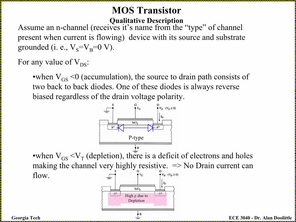
Assume an n-channel (receives it’s name from the “type” of channel present when current is flowing) device with its source and substrate grounded (i. e., VS=VB=0 V).
For any value of VDS:
•when VGS <0 (accumulation), the source to drain path consists of two back to back diodes. One of these diodes is always reverse biased regardless of the drain voltage polarity.
•when VGS <VT (depletion), there is a deficit of electrons and holes making the channel very highly resistive. => No Drain current can flow.
High ρ due to Depletion

ECE 3040 - Dr. Alan DoolittleGeorgia Tech
MOS TransistorQualitative Description
Consider now the Inversion case:
First, VDS = 0:
•when VGS > VT , an induced n- type region, an “inversion layer”, forms in the channel and “electrically connects” the source and drain.
P-type
Inversion layer (n-type)

ECE 3040 - Dr. Alan DoolittleGeorgia Tech
MOS TransistorQualitative Description
Inversion case, VGS > VT(continued):
When VDS >0 , the induced n- type region allows current to flow between the source and drain. The induced channel astlike a simple resistor. Thus, this current, ID, depends linearly on the Drain voltage VD. This mode of operation is called the linear or “triode”* region.
P-type
Inversion layer (n-type)
* “Triode” is a historical term from vacuum tube technology.

ECE 3040 - Dr. Alan DoolittleGeorgia Tech
Inversion case, VGS > VT(continued):
Drain current verses drain voltage when in the linear or “triode”* region.
MOS TransistorQualitative Description

ECE 3040 - Dr. Alan DoolittleGeorgia Tech
MOS TransistorQualitative Description
Inversion case, VGS > VT(continued):
When VDS increases a few tenths of a volt (>0):
•The depletion region near the drain widens (N+ drain is positively biased – I.e. reverse biased with respect to the substrate).
•The electron concentration in the inversion layer near the drain decreases as they are “sucked out” by the Drain voltage.
•Channel conductance decreases resulting in a drop in the slope of the ID-VD curve.
P-type
Reduced electron concentration in the Inversion layer near the drain

ECE 3040 - Dr. Alan DoolittleGeorgia Tech
Inversion case, VGS > VT(continued):
Drain current verses drain voltage for increasing VDS (still in the “linear” or triode region).
MOS TransistorQualitative Description

ECE 3040 - Dr. Alan DoolittleGeorgia Tech
MOS TransistorQualitative Description
Inversion case, VGS > VT(continued):
The inversion layer eventually vanishes near the drain end of the channel.
This is called “Pinch-Off” and results in a Flat ID-VDS curve

ECE 3040 - Dr. Alan DoolittleGeorgia Tech
Inversion case, VGS > VT(continued):
ID-VDS curve for the “Saturation Region”The drain-source voltage, VDS, at which this occurs is called the saturation voltage, Vsat while the current is called the saturation current, IDsat.
MOS TransistorQualitative Description
IDsat

ECE 3040 - Dr. Alan DoolittleGeorgia Tech
MOS TransistorQualitative Description
Inversion case, VGS > VT(continued):
For VDS>Vsat the channel length, L, effectively changes by a value ∆L.
The region of the channel, ∆L is depleted and thus, is high resistivity. Accordingly, almost all voltage increases in VDS>Vsat are “dropped across” this portion of the channel.
High electric fields in this region act similarly to the collector-base junction in a BJT in active mode, “stripping” or “collecting” carriers from the channel.

ECE 3040 - Dr. Alan DoolittleGeorgia Tech
MOS TransistorQualitative Description
Inversion case, VGS > VT(continued):
If ∆L<<L, the voltage at the end of the channel will be constant (Vsat ) for all VDS>Vsat. ID will be constant.
If ∆L~L, the voltage dropped across the the channel (VSAT) varies greatly with VDS due to large modulations in the electric field across the pinched off region ( E=[VDS-VSAT]/[∆L]). In this case, ID increases slightly with VDS.

ECE 3040 - Dr. Alan DoolittleGeorgia Tech
MOS TransistorQualitative Description
Finally,
ID-VDS curves for various VGS:
VDsat depends on VG

ECE 3040 - Dr. Alan DoolittleGeorgia Tech
MOS Transistor I-V Derivation
With our expression relating the Gate voltage to the surface potential and the fact that φS=2φF we can determine the value of the threshold voltage
( )
( )
areaunit per ecapacitanc oxide theis
where,
devices) channel-p(for 222
devices) channel-n(for 22
2
ox
oxox
FS
D
ox
SFT
FS
A
ox
SFT
xC
qNC
V
qNC
V
ε
φε
εφ
φε
εφ
=
−−=
+=
Where we have made use of the use of the expression,
oSS K εε =

ECE 3040 - Dr. Alan DoolittleGeorgia Tech
MOS Transistor I-V Derivation
Coordinate Definitions for our “NMOS” Transistor
x=depth into the semiconductor from the oxide interface.
y=length along the channel from the source contact
z=width of the channel
xc(y) = channel depth (varies along the length of the channel).
n(x,y)= electron concentration at point (x,y)
µn(x,y)=the mobility of the carriers at point (x,y)
Device width is Z
Channel Length is L
Assume a “Long Channel” device (for now do not worry about the channel length modulation effect)

ECE 3040 - Dr. Alan DoolittleGeorgia Tech
MOS Transistor I-V DerivationConcept of Effective mobilityThe mobility of carriers near the interface is significantly lower than carriers in the semiconductor bulk due to interface scattering.
Since the electron concentration also varies with position, the average mobility of electrons in the channel, known as the effective mobility, can be calculated by a weighted average,
[ ]
∫
∫
∫∫
=
=
=
=
=
=
=
=
−=
−=
=
)(
0
2)(
0
)(
0
)(
0
),(),()(
/arg),()(
,
),(
),(),(
yxx
x nN
n
yxx
xN
yxx
x
yxx
x nn
c
c
c
c
dxyxnyxyQ
q
cmechdxyxnqyQ
definingor
dxyxn
dxyxnyx
µµ
µµ
Empirically
( )constants are ,
1θµ
θµµ
andwhereVV
o
TGS
on −+
=

ECE 3040 - Dr. Alan DoolittleGeorgia Tech
MOS Transistor I-V Derivation
Drain Current-Voltage RelationshipIn the Linear Region, VGS>VT and 0<VDS<Vdsat
dydnqnEqJJ
nqDnEqJ
nynNyN
NnN
φµµ
µ
−≅≅≅
∇+=
Neglecting the diffusion current, and recognizing the current isonly in the y-direction,

ECE 3040 - Dr. Alan DoolittleGeorgia Tech
MOS Transistor I-V Derivation
Drain Current-Voltage RelationshipIn the Linear Region, VGS>VT and 0<VDS<Vdsat
∫
∫
∫∫
∫
∫ ∫∫
=
=
=
=
=
=
=
=
=
=
=
=
−=
−=
−=
−=
−
−=
=−=
DS
DS
DS
c
c
V
Nn
D
V
NnD
V
Nn
Ly
y D
Nn
yxx
x n
yxx
x NyNyD
dQLZI
dQZLI
dQZdyI
dydQZ
dxyxnyxqdydZ
dxJZdxdzJI
φ
φ
φ
φ
φ
φ
φµ
φµ
φµ
φµ
µφ
0
0
00
)(
0
)(
0
),(),(
To find ID, we need an expression relating φ and QN

ECE 3040 - Dr. Alan DoolittleGeorgia Tech
MOS Transistor I-V Derivation“Capacitor-Like” Model for QNAssumptions:•Neglect all but the mobile inversion charge•For the MOSFET, the charge in the semiconductor is a linear function of position along the semiconductor side of the plate. Thus, φ varies from 0 to VDS
MOS Capacitor MOS Transistor
( ) TGS VVfor ≥−−≅ TGSoxN VVCQ( )
TGS VVfor ≥−−−≅ φTGSoxN VVCQ
Source Drain
,dVdQCSince ox =
Neglect the depletion region chargeNote: Assuming a linear variation of potential along the channelleads to an underestimation of current but is a good estimate for hand calculations.
Only voltages above threshold create inversion charge

ECE 3040 - Dr. Alan DoolittleGeorgia Tech
MOS Transistor I-V Derivation
Using “Capacitor-Like” Model for QN we can estimate ID as:
( )
( ) TGSDsatDSDS
DSTGSoxn
D
V
TGoxn
D
V
Nn
D
VVandVVV
VVVLCZ
I
dVVCLZ
I
dQLZ
I
DS
DS
≥≤≤
−−=
−−−−
=
−=
∫
∫=
=
=
=
02
2
0
0
µ
φφµ
φµ
φ
φ
φ
φ
This is known as the “square law” describing the Current-Voltage characteristics in the “Linear” or
“Triode” region.Note the linear behavior for small VDS (can neglect VDS
2 term). Note the negative parabolic dependence for larger VDS but still VDS<VDsat(can NOT neglect VDS
2 term).

ECE 3040 - Dr. Alan DoolittleGeorgia Tech
MOS Transistor I-V Derivation
“Capacitor-Like” Model for QN
For VDS>Vdsat the voltage drop across our channel is VDsat with the remaining voltage (VDS-VDsat) dropped across the pinch-off region
( ) DSDsatDsat
DsatTGSoxn
DsatD VVV
VVVLCZ
II ≤
−−==
2
2µ
But the charge at the end of the channel is zero due to the pinched off channel,
( )
DsatTGS
DsatTGSoxN
VVVor
VVVCLyQ
=−
=−−−≅= 0)(
Thus,
( )[ ] DSDsatTGSoxn
DsatD VVVVLCZ
II ≤−== 2
2µ
But what about the saturation region?

ECE 3040 - Dr. Alan DoolittleGeorgia Tech
MOS Transistor I-V Derivation
TGSDsat VVV −=
( )[ ] DSDsatTGSoxn
DsatD VVVVLCZ
II ≤−== 2
2µ
( )
TGSDsatDS
DSDSTGS
oxnD
VVandVV
VVVV
LCZ
I
≥≤≤
−−=
02
2µ
Summary of MOSFET IV Relationship

ECE 3040 - Dr. Alan DoolittleGeorgia Tech
MOS Transistor Applications
Voltage variable ResistorAn n-channel MOSFET has a gate width to length ratio of Z/L=100, un=200 cm2/Vsec, Cox=0.166 uF/cm2 and VT=1V. We want to develop a resistor that has a resistance that is controlled by an external voltage. Such a device would be used in “variable gain amplifiers”, “automatic gain control devices”, “compressors” and many other electronic devices. Define what range of VDS must be maintained to achieve proper “voltage variable resistance” operation. Find the “On-resistance”(VDS/ID) of the transistor from 1.5V<VGS<4Vfor small VDS .
First, to achieve voltage variable resistance operation, we must operate in the linear region. Otherwise, the current is either a constant regardless of drain voltage (saturation region) or is approximately zero (accumulation and depletion).
Thus, VGS -VT>VDS. Given the values above, 0<VDS<0.5V
Continued...

ECE 3040 - Dr. Alan DoolittleGeorgia Tech
MOS Transistor Applications
Voltage variable ResistorUsing the linear region ID equation:
( ) ( )[ ]
( )[ ] ( )[ ]
( ) ( )[ ]
Ω≤≤Ω
−−=
−=
−==
−≈
−−=
600100,
1/6166.020001.0
V smallfor 2
2
DS
2
DS
GSDS
TGSoxnDSTGS
oxn
DS
D
DSDS
DSTGSoxnDS
DSTGSoxn
D
RThus
VcmFeR
VVCZ
L
VVVLCZ
VI
VR
VVVLCZV
VVVLCZ
I
µµ
µµ
ECE 3040 - Dr. Alan DoolittleGeorgia Tech
MOS Transistor Applications
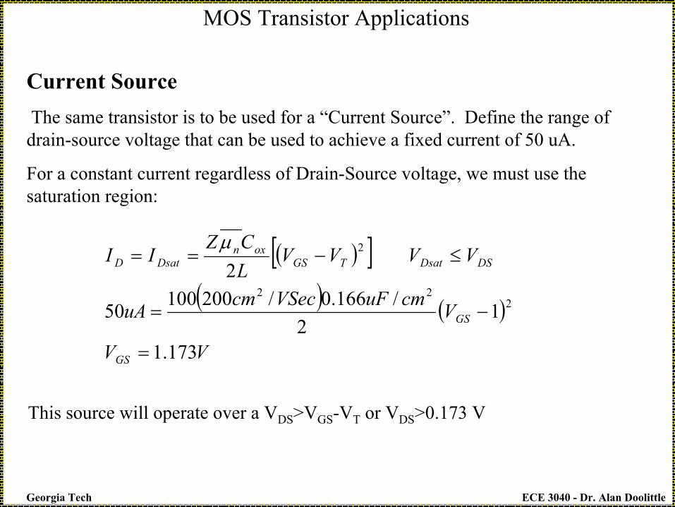
Current SourceThe same transistor is to be used for a “Current Source”. Define the range of
drain-source voltage that can be used to achieve a fixed current of 50 uA.
For a constant current regardless of Drain-Source voltage, we must use the saturation region:
( )[ ]( ) ( )
VV
VcmuFVSeccmuA
VVVVLCZ
II
GS
GS
DSDsatTGSoxn
DsatD
173.1
12
/166.0/20010050
22
22
2
=
−=
≤−==µ
This source will operate over a VDS>VGS-VT or VDS>0.173 V

ECE 3040 - Dr. Alan DoolittleGeorgia Tech
MOS Transistor: Deviations From IdealChannel Length Modulation Effect
Above “pinch-off” (when VDS>VDsat=VGS-VT) the channel length reduces by a value ∆L.
Thus, the expression for drain current,
Becomes,
( )[ ] DSDsatTGSoxn
DsatD VVVVLCZ
II ≤−== 2
2µ
( ) ( )[ ]
( )[ ] DSDsatTGSoxn
DsatD
DSDsatTGSoxn
DsatD
VVLLVV
LCZII
LL
LLL
VVVVLL
CZII
≤
∆
+−==
∆
+≅∆−
⟨⟨∆
≤−∆−
==
12
111 L,L *sinceor
2
2
2
µ
µ
*In many modern devices, this assumption does not hold. Thus, the channel length modulation parameter we are deriving does not describe the IV expressions well.

ECE 3040 - Dr. Alan DoolittleGeorgia Tech
MOS Transistor: Deviations From IdealChannel Length Modulation Effect
DSVLL λ=
∆
But the fraction of the channel that is pinched off depends linearly on VDS because the voltage across the pinch-off region is (VDS-VDsat) so,
( )[ ]( ) DSDsatDSTGSoxn
DsatD VVVVVLCZ
II ≤+−== λµ
12
2
where λ is known as the Channel-Length Modulation parameter and is typically: 0.001 V-1 < λ <0.1 V−1
Channel Length Modulation causes the dependence of drain current on the drain voltage in saturation.

ECE 3040 - Dr. Alan DoolittleGeorgia Tech
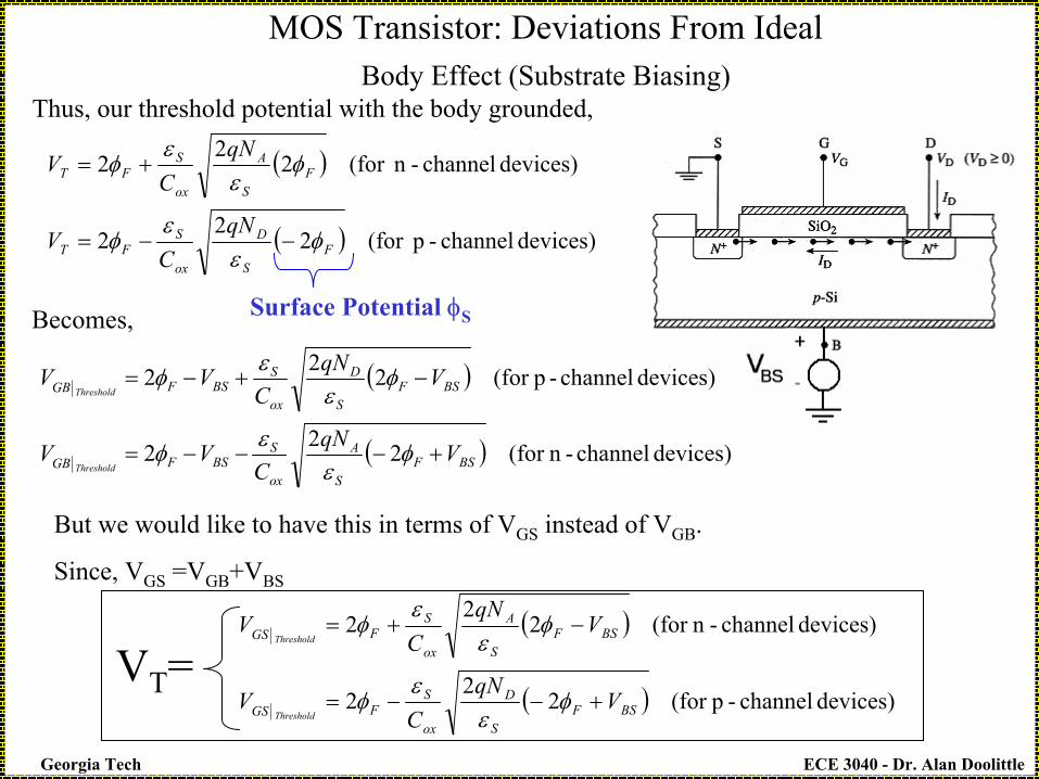
MOS Transistor: Deviations From IdealBody Effect (Substrate Biasing)
Until now, we have only considered the case where the substrate (Body) has been grounded….
…but the substrate (Body) is often intentionally biased such that the Source-Body and Drain-Body junctions are reversed biased.
The body bias, VBS, is known as the backgate bias and can be used to modify the threshold voltage.
Note that now our channel potential has an offset equal to VBS, ….
ECE 3040 - Dr. Alan DoolittleGeorgia Tech
( )
( ) devices) channel-p(for 22
2
devices) channel-n (for222
FS
D
ox
SFT
FS
A
ox
SFT
qNC
V
qNC
V
φε
εφ
φε
εφ
−−=
+=
MOS Transistor: Deviations From IdealBody Effect (Substrate Biasing)
Thus, our threshold potential with the body grounded,
Becomes,
( )
( ) devices) channel-n(for 222
devices) channel-p(for 222
BSFS
A
ox
SBSFGB
BSFS
D
ox
SBSFGB
VqNC
VV
VqNC
VV
Threshold
Threshold
+−−−=
−+−=
φε
εφ
φε
εφ
But we would like to have this in terms of VGS instead of VGB.
Since, VGS =VGB+VBS
( )
( ) devices) channel-p(for 22
2
devices) channel-n(for 222
BSFS
D
ox
SFGS
BSFS
A
ox
SFGS
VqN
CV
VqNC
V
Threshold
Threshold
+−−=
−+=
φε
εφ
φε
εφ
Surface Potential φS
VT=
ECE 3040 - Dr. Alan DoolittleGeorgia Tech
MOS Transistor: Deviations From IdealBody Effect (Substrate Biasing)
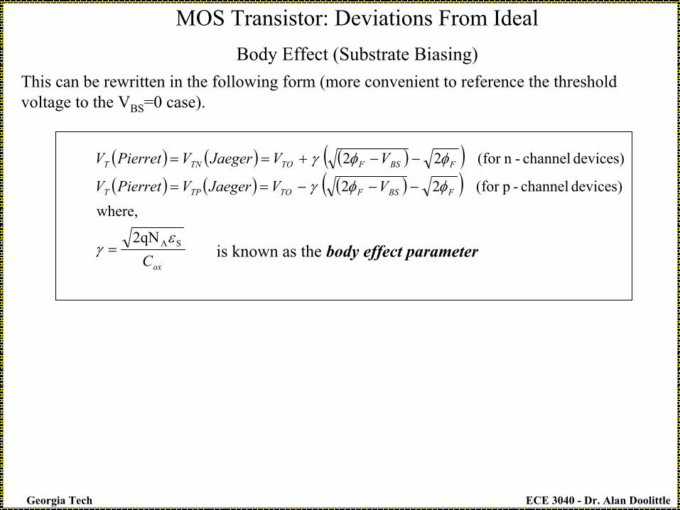
( ) ( ) ( )( )( ) ( ) ( )( )
ox
FBSFTOTPT
FBSFTOTNT
C
VVJaegerVPierretV
VVJaegerVPierretV
SA2qN
where,devices) channel-p(for 22
devices) channel-n(for 22
εγ
φφγ
φφγ
=
−−−==
−−+==
This can be rewritten in the following form (more convenient to reference the threshold voltage to the VBS=0 case).
is known as the body effect parameter

ECE 3040 - Dr. Alan DoolittleGeorgia Tech
MOS Transistor:
Enhancement Mode verses Depletion Mode MOSFET
We have been studying the “enhancement mode” MOSFET (Metal-Oxide-Semiconductor Field Effect Transistor). It is called “enhancement” because conduction occurs only after the channel conductance is “improved” or “enhanced”. In this case,
VTN>0 and VTP<0
Transistors can be fabricated such that:
These transistors have conduction for VGS=0 due to a channel already existing without the need to “invert the near surface region”. To modulate currents, a field must applied to the gate that depletes the channel. Thus, transistors of this nature arecalled “Depletion mode MOSFETs”.
0V and 0V TPTN ≥≤
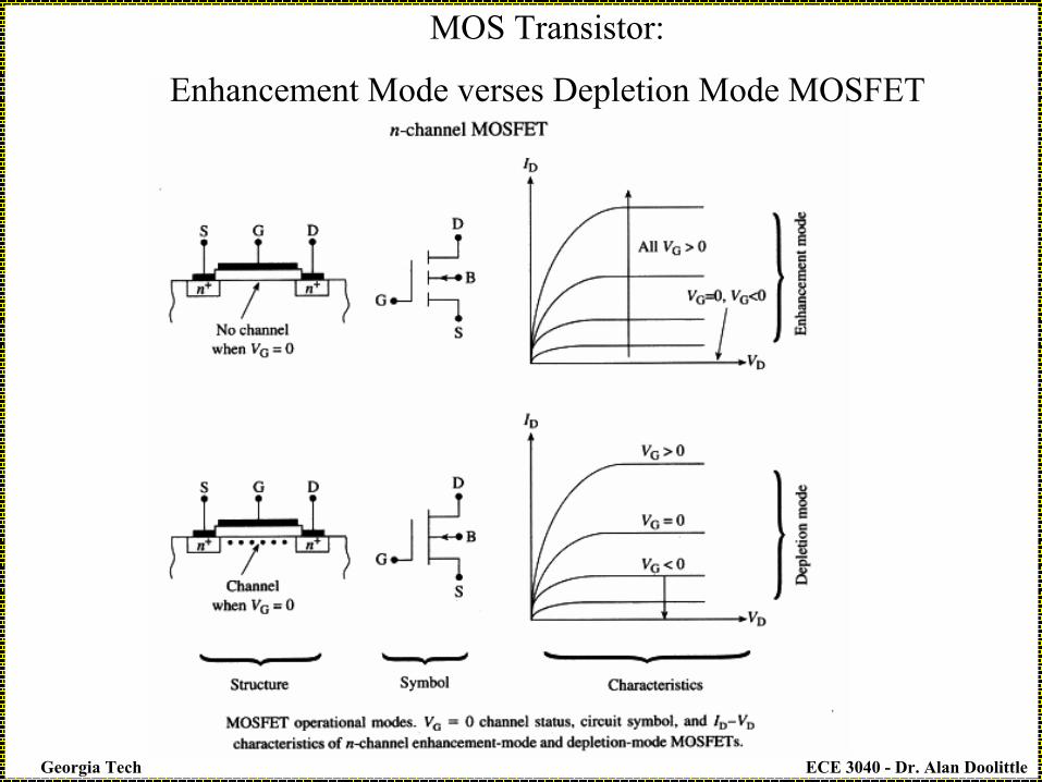
ECE 3040 - Dr. Alan DoolittleGeorgia Tech
MOS Transistor:
Enhancement Mode verses Depletion Mode MOSFET

ECE 3040 - Dr. Alan DoolittleGeorgia Tech
MOS Transistor: Summary
Jaeger uses the notation:
Pierret)in (Z Width Gate theis W where
PMOS
Pierret)in (Z Width Gate theis W where
'
'
LWC
LWKK
LWC
LWKK
NMOS
oxnpp
oxnnn
µ
µ
==
==
4-Terminal 3-Terminal
NMOS(n-channel)
PMOS(p-channel)
Enhancement EnhancementDepletion Depletion

ECE 3040 - Dr. Alan DoolittleGeorgia Tech
MOS Transistor: Summary
VT for Depletion Mode
VT for Enhancement Mode
Threshold Voltage
Saturation
Linear
Cutoff
Regardless of Mode
PMOSNMOS
Pierret)in Z W:(Note ' ===L
WCL
WKK oxnnn µ Pierret)in Z W:(Note ' ===L
WCL
WKK oxnpp µ
TNGSDS Vvfori ≤= 0 TPSGDS Vvfori −≤= 0
( )[ ]( )
0
12
2
≥−≥
+−=
TNGSDS
DSTNGSoxn
DS
Vvvfor
vVvLCZ
i λµ ( )[ ]( )
0
12
2
≥+≥
++=
TPSGSD
SDTPSGoxn
DS
Vvvfor
vVvLCZi λµ
( )
02
2
≥≥−
−−=
DSTNGS
DSDSTNGS
oxnDS
vVv
vvVv
LCZ
iµ ( )
02
2
≥≥+
−−=
SDTPSG
SDSDTPSG
oxnSD
vVv
vvVv
LCZ
iµ
0>TNV
0≤TNV
0<TPV
0≥TPV
( )( )FBSFTOTP vVV φφγ 22 −+−=( )( )FBSFTOTN vVV φφγ 22 −−+=

ECE 3040 - Dr. Alan DoolittleGeorgia Tech
MOSFET Small Signal Model and Analysis
•Just as we did with the BJT, we can consider the MOSFET amplifier analysis in two parts:
•Find the DC operating point
•Then determine the amplifier output parameters for very small input signals.

ECE 3040 - Dr. Alan DoolittleGeorgia Tech
MOSFET Small Signal Model and Analysis
Linear Two Port Network
+V1
-
i1 i2+V2
-
I1=y11V1 + y12V2
I2=y21V1 + y22V2
General “y-parameter” Network
Non-Linear I-V relationship
(BJT, MOSFET,
etc…)
+V1
-
i1 i2+V2
-
Linearizeover “small
signal range”
IGS=y11VGS + y12VDS
IDS=y21VGS + y22VDS
MOSFET “y-parameter” Network
vGS
vDS
iDS
iGS

ECE 3040 - Dr. Alan DoolittleGeorgia Tech
IGS=y11VGS + y12VDS
IDS=y21VGS + y22VDS
[ [ [IGS y11 y12 VGS
IDS y21 y22 VDS
[[[
=QVQVi
jij
DSGSVI
y,,,
∂
∂=
Derivative of current-voltage equation evaluated at the Quiescent Point
MOSFET Small Signal Model and Analysis
( )[ ]( ) TNGSDSDSTNGSn
DS VVVforVVVK
I −≥+−= λ12
2
MOSFET Amplifiers are biased into Saturation (or Active Mode)
1.) Input Conductance
2.) Output Conductance
3.) Transconductance
00000 1211 ==⇒=∂∂
=∂∂
⇒= yandyVI
andVI
IDS
GS
GS
GSGS
( )222 2 TGS
n
DS
DS VVK
yVI
−==∂∂ λ
( )( )DSTGSnGS
DS VVVKyVI
λ+−==∂∂
121

ECE 3040 - Dr. Alan DoolittleGeorgia Tech
MOSFET Small Signal Model and AnalysisCompare with BJT Results
( )DS
DSTGS
no
V
IVV
Kgy
+=−==
λ
λ12
222
( )( )
−
=+−==
2
121TNGS
DSDSTGSnm VV
IVVVKgy λ
CEA
C
VVI
y+
=22
T
C
VI
y =21
MOSFET BJT
There is a large amount of symmetry between the MOSFET and the BJT
Each of these parameters act in the
same manner
ECE 3040 - Dr. Alan DoolittleGeorgia Tech
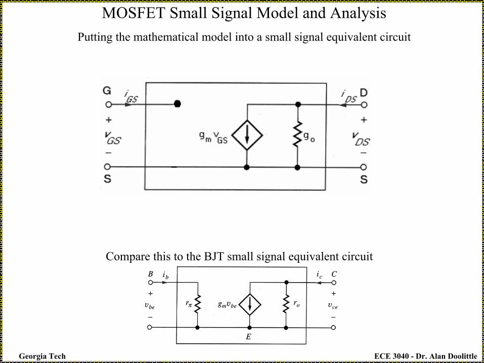
MOSFET Small Signal Model and AnalysisPutting the mathematical model into a small signal equivalent circuit
Compare this to the BJT small signal equivalent circuit
ECE 3040 - Dr. Alan DoolittleGeorgia Tech
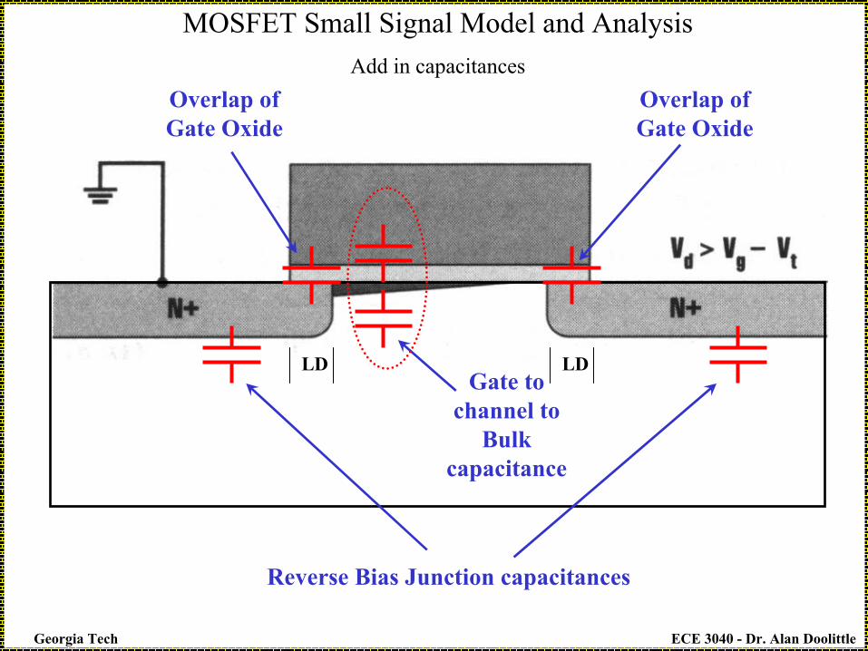
MOSFET Small Signal Model and AnalysisAdd in capacitances
Reverse Bias Junction capacitances
Overlap of Gate Oxide
Gate to channel to
Bulk capacitance
Overlap of Gate Oxide
LD LD

ECE 3040 - Dr. Alan DoolittleGeorgia Tech
MOSFET Small Signal Model and AnalysisComplete Model of a MOSFET
Reverse Bias Junction capacitances
Overlap of Gate Oxide and Gate to
channel capacitance
Overlap of Gate Oxide
Gate to channel to
Bulk capacitance
FSBmmb V
ggφ
γ22 +
=Due to effective modulation of the threshold voltage.