
Measuring System Mass and Material Density of MEMS by ...
4
Measuring System Mass and Material Density of MEMS by Measuring Capacitance and Resonant Frequency: Simulated Experiment Aarti Chigullapalli 1 , Jason V. Clark 1,2 1 School of Mechanical Engineering, 2 School of Electrical and Computer Engineering, Discovery Park, Purdue University, West Lafayette, Indiana, USA ABSTRACT In this paper we present a method to measure the system mass and material density of MEMS with comb drives by measuring resonant frequency and the changes in capacitance to close two asymmetric gaps. To measure mass we (1) determine the change in geometry in going from layout to fabrication to characterize displacement, (2) characterize the comb drive force to determine stiffness, and (3) divide stiffness by resonance frequency to measure system mass. To measure material density we divide system mass by system volume, which we determine by our modified Raleigh-Ritz method. We validate our measurement using a method we call simulated experiment. A simulated experiment involves simulating the kind of measurements that would only be available in a true experiment to characterize the device. It then becomes a trivial matter to compare our results to actual properties of the device, which is otherwise difficult to do in a true experiment due to a lack of precise measurement standards for MEMS. Our results are less than 1% of our computer model. Keywords: mass, density, simulated experiment, electro micro metrology, EMM 1. INTRODUCTION For dynamical microelectromechanical systems (MEMS), performance depends highly on system mass. By measuring system mass, the response of a device might be better understood. And by measuring material density, the quality of fabrication might be better controlled. For MEMS accelerometers and gyroscopes, knowledge of system mass is useful for measuring applied forces or accelerations [1]. There have been several efforts to measure system mass by others. For instance, in [2] and [3] mass was measured by measuring the frequency shift caused by depositing 500nm latex spheres onto a MEMS resonator. In [4] they compared the difference in cantilever resonance before and after the deposition chromium on an atomic force microscope (AFM) cantilever. Additional uncertainty arises when system stiffness is used in the analysis because conventional methods to measure stiffness are uncertain by 5% to 40% [5] [6]. In most conventional measurement methods, the uncertainty is often greater than 10% and the accuracy is often unknown. Conversely, it appears that very little research has been conducted on local measurements of density of commonly used MEMS materials. However, global (or averaged) measurements of density can be done by performing macroscale measurements of geometry and mass of bulk material. However, it is expected that the density of many MEMS materials varies between facilities, between runs, between wafers, and may possibly vary about the wafer itself. In this paper we propose a method to measure system mass and material density of MEMS with comb drives. MEMS without comb drives may benefit from such measurements if they are fabricated within close proximity to the test structures, such that they would be likely to share much of the same material properties and overcut errors. Our method facilitates electronic probing for industrial-scale batch fabrication, or post-packaged on-chip measurements for self-calibration. Our method includes measuring the change in capacitance to close two asymmetric gaps and measuring the resonant frequency. Measurements of the gaps are used to determine geometry, system volume, displacement, comb drive force, and stiffness. The measurement of frequency is used to determine system mass. We NSTI-Nanotech 2012, www.nsti.org, ISBN 978-1-4665-6275-2 Vol. 2, 2012 196
Transcript of Measuring System Mass and Material Density of MEMS by ...

Measuring System Mass and Material Density of MEMS by Measuring Capacitance and Resonant Frequency: Simulated Experiment
Aarti Chigullapalli1, Jason V. Clark1,2
1School of Mechanical Engineering, 2School of Electrical and Computer Engineering, Discovery Park, Purdue University, West Lafayette, Indiana, USA
ABSTRACT
In this paper we present a method to measure the system mass and material density of MEMS with comb drives by measuring resonant frequency and the changes in capacitance to close two asymmetric gaps. To measure mass we (1) determine the change in geometry in going from layout to fabrication to characterize displacement, (2) characterize the comb drive force to determine stiffness, and (3) divide stiffness by resonance frequency to measure system mass. To measure material density we divide system mass by system volume, which we determine by our modified Raleigh-Ritz method. We validate our measurement using a method we call simulated experiment. A simulated experiment involves simulating the kind of measurements that would only be available in a true experiment to characterize the device. It then becomes a trivial matter to compare our results to actual properties of the device, which is otherwise difficult to do in a true experiment due to a lack of precise measurement standards for MEMS. Our results are less than 1% of our computer model.
Keywords: mass, density, simulated experiment, electro micro metrology, EMM
1. INTRODUCTION
For dynamical microelectromechanical systems (MEMS), performance depends highly on system mass. By measuring system mass, the response of a device might be better understood. And by measuring material density, the quality of fabrication might be better controlled. For MEMS accelerometers and gyroscopes, knowledge of system mass is useful for measuring applied forces or accelerations [1].
There have been several efforts to measure system mass by others. For instance, in [2] and [3] mass was measured by measuring the frequency shift caused by depositing 500nm latex spheres onto a MEMS resonator. In [4] they compared the difference in cantilever resonance before and after the deposition chromium on an atomic force microscope (AFM) cantilever. Additional uncertainty arises when system stiffness is used in the analysis because conventional methods to measure stiffness are uncertain by 5% to 40% [5] [6]. In most conventional measurement methods, the uncertainty is often greater than 10% and the accuracy is often unknown.
Conversely, it appears that very little research has been conducted on local measurements of density of commonly used MEMS materials. However, global (or averaged) measurements of density can be done by performing macroscale measurements of geometry and mass of bulk material. However, it is expected that the density of many MEMS materials varies between facilities, between runs, between wafers, and may possibly vary about the wafer itself.
In this paper we propose a method to measure system mass and material density of MEMS with comb drives. MEMS without comb drives may benefit from such measurements if they are fabricated within close proximity to the test structures, such that they would be likely to share much of the same material properties and overcut errors. Our method facilitates electronic probing for industrial-scale batch fabrication, or post-packaged on-chip measurements for self-calibration. Our method includes measuring the change in capacitance to close two asymmetric gaps and measuring the resonant frequency. Measurements of the gaps are used to determine geometry, system volume, displacement, comb drive force, and stiffness. The measurement of frequency is used to determine system mass. We
NSTI-Nanotech 2012, www.nsti.org, ISBN 978-1-4665-6275-2 Vol. 2, 2012196
virtually validate our method by using a simulated experiment, in which we emulate experimental methods by simulation to extract the mass and density of our computer model and compare the results against the models true parameters. True experimental validation is presently difficult due to a lack of accurate and precise ASTM measurement standards for microscale mass and material density.
The rest of the paper is organized as follows. In Section 2 we describe our method for measuring system mass and density. In Section 3 we describe our simulated experiment. Results are provided in Section 4. We conclude our findings in Section 5.
2. MASS AND DENSITY
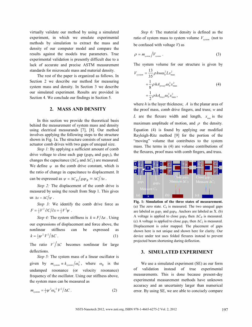
In this section we provide the theoretical basis behind the measurement of system mass and density using electrical measurands [7], [8]. Our method involves applying the following steps to the structure shown in Fig. 1a. The structure consists of sensor and actuator comb drives with two gaps of unequal size.
Step 1: By applying a sufficient amount of comb drive voltage to close each gap (gapR and gapL), the changes the capacitance (CR and CL) are measured. We define as the comb drive constant, which is the ratio of change in capacitance to displacement. It can be expressed as R RC gap C x .
Step 2: The displacement of the comb drive is measured by using the result from Step 1. This gives us x C .
Step 3: We identify the comb drive force as 2 21 1
2 2F V C x V .
Step 4: The system stiffness is k F x . Using our expressions of displacement and force above, the nonlinear stiffness can be expressed as
2 212k V C . (1)
The ratio 2V C becomes nonlinear for large deflections.
Step 5: The system mass of a linear oscillator is given by
20system systemm k , where 0 is the
undamped resonance (or velocity resonance) frequency of the oscillator. Using our stiffness above, the system mass can be measured as
2 2 2102systemm V C . (2)
Step 6: The material density is defined as the ratio of system mass to system volume systemV (not to
be confused with voltage V) as
system systemm V . (3)
The system volume for our structure is given by
2 20 max
2 20 max
2 20 max
1335181 ,2
system
proof
truss
V hw Lx
hA x
hA x
(4)
where h is the layer thickness; A is the planar area of the proof mass, comb drive fingers, and truss; w and L are the flexure width and length, maxx is the
maximum amplitude of motion, and the density. Equation (4) is found by applying our modified Rayleigh-Ritz method [9] for the portion of the “moving” volume that contributes to the system mass. The terms in (4) are volume contributions of the flexures, proof mass with comb fingers, and truss.
Fig. 1: Simulation of the three states of measurement. (a) The zero state. C0 is measured. The two unequal gaps are labeled as gapL and gapR. Anchors are labeled as X. (b) A voltage is applied to close gapR then ∆CR is measured. (c) A voltage is applied to close gapL then ∆CL is measured. Displacement is color mapped. The placement of gaps shown here is not unique and shown here for clarity. Our device under test uses folded flexures instead to prevent projected beam shortening during deflection.
3. SIMULATED EXPERIMENT
We use a simulated experiment (SE) as our form of validation instead of true experimental measurements. This is done because present-day experimental measurement methods have unknown accuracy and an uncertainty larger than numerical error. By using SE, we are able to concisely compare
NSTI-Nanotech 2012, www.nsti.org, ISBN 978-1-4665-6275-2 Vol. 2, 2012 197
the predicted system mass and density of our metrology method against that of our computer model. We emulate the experimental measurements of capacitance and resonance frequency, which are commonly electrically-probed measurements in true experiments.
We use a finite element analysis tool to model the mechanical and electrical physics. As discussed in Section 2, we measure geometry by closing 2 unequal gaps, measure the comb drive constant, and measure resonant frequency as would be done in a real experiment. By substituting values in (2) and (3), we are able to predict the system mass and material density of our model, and validate it against our model’s true parameters.
4. RESULTS
Comb drive constant. To maximize precision
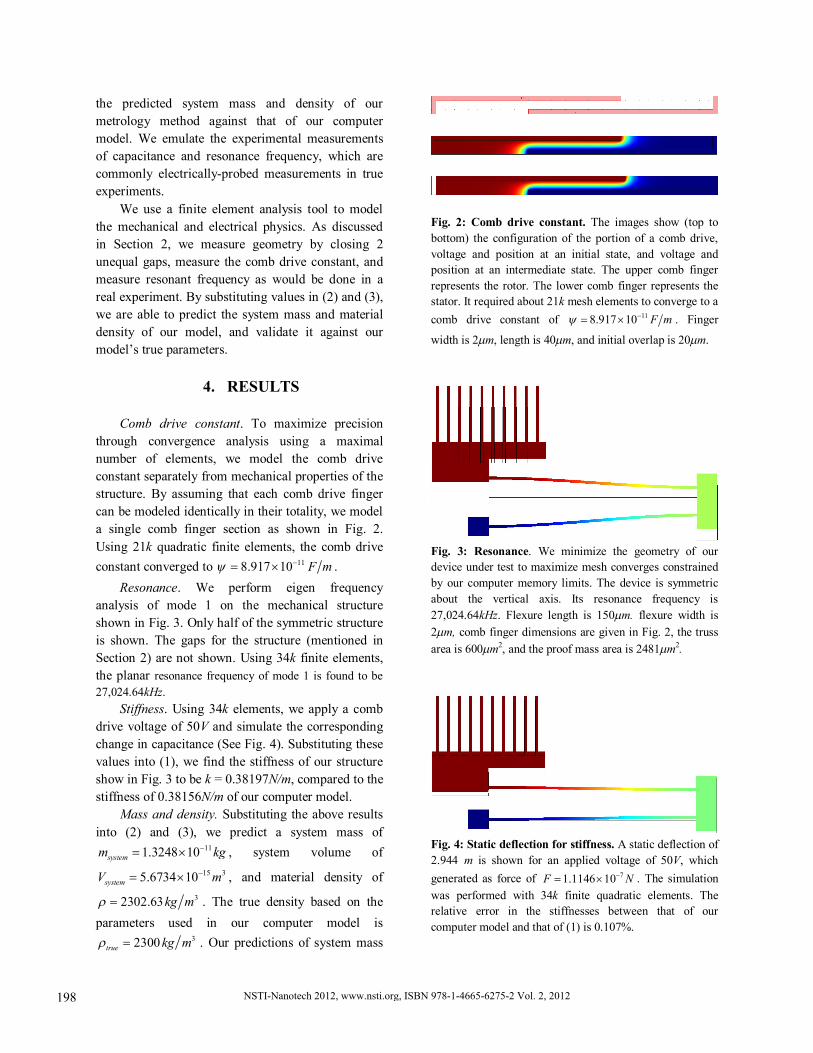
through convergence analysis using a maximal number of elements, we model the comb drive constant separately from mechanical properties of the structure. By assuming that each comb drive finger can be modeled identically in their totality, we model a single comb finger section as shown in Fig. 2. Using 21k quadratic finite elements, the comb drive constant converged to 118.917 10 F m .
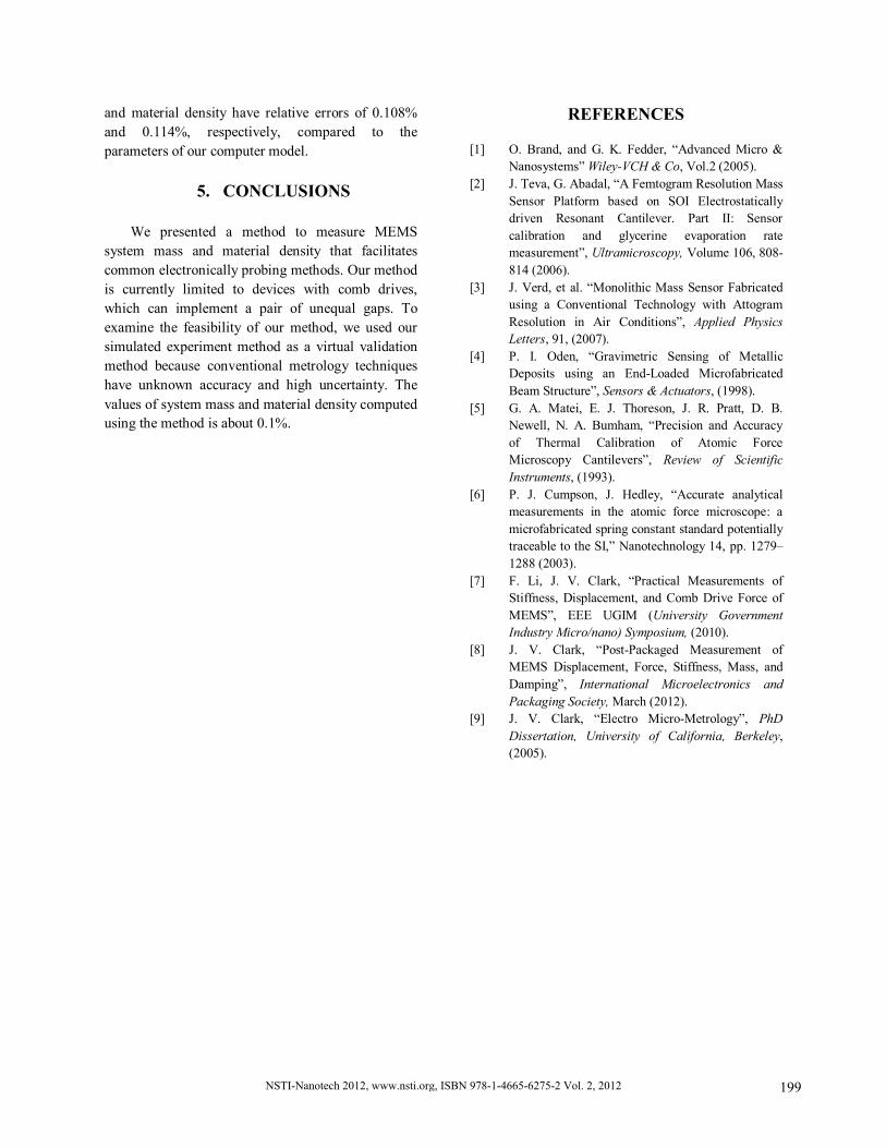
Resonance. We perform eigen frequency analysis of mode 1 on the mechanical structure shown in Fig. 3. Only half of the symmetric structure is shown. The gaps for the structure (mentioned in Section 2) are not shown. Using 34k finite elements, the planar resonance frequency of mode 1 is found to be 27,024.64kHz.
Stiffness. Using 34k elements, we apply a comb drive voltage of 50V and simulate the corresponding change in capacitance (See Fig. 4). Substituting these values into (1), we find the stiffness of our structure show in Fig. 3 to be k = 0.38197N/m, compared to the stiffness of 0.38156N/m of our computer model.
Mass and density. Substituting the above results into (2) and (3), we predict a system mass of
111.3248 10systemm kg , system volume of 15 35.6734 10systemV m , and material density of
32302.63kg m . The true density based on the parameters used in our computer model is
32300true kg m . Our predictions of system mass
Fig. 2: Comb drive constant. The images show (top to bottom) the configuration of the portion of a comb drive, voltage and position at an initial state, and voltage and position at an intermediate state. The upper comb finger represents the rotor. The lower comb finger represents the stator. It required about 21k mesh elements to converge to a comb drive constant of 118.917 10 F m . Finger
width is 2m, length is 40m, and initial overlap is 20m.
Fig. 3: Resonance. We minimize the geometry of our device under test to maximize mesh converges constrained by our computer memory limits. The device is symmetric about the vertical axis. Its resonance frequency is 27,024.64kHz. Flexure length is 150m. flexure width is 2m, comb finger dimensions are given in Fig. 2, the truss area is 600m2, and the proof mass area is 2481m2.
Fig. 4: Static deflection for stiffness. A static deflection of 2.944µm is shown for an applied voltage of 50V, which generated as force of 71.1146 10F N . The simulation was performed with 34k finite quadratic elements. The relative error in the stiffnesses between that of our computer model and that of (1) is 0.107%.
NSTI-Nanotech 2012, www.nsti.org, ISBN 978-1-4665-6275-2 Vol. 2, 2012198
and material density have relative errors of 0.108% and 0.114%, respectively, compared to the parameters of our computer model.
5. CONCLUSIONS
We presented a method to measure MEMS
system mass and material density that facilitates common electronically probing methods. Our method is currently limited to devices with comb drives, which can implement a pair of unequal gaps. To examine the feasibility of our method, we used our simulated experiment method as a virtual validation method because conventional metrology techniques have unknown accuracy and high uncertainty. The values of system mass and material density computed using the method is about 0.1%.
REFERENCES
[1] O. Brand, and G. K. Fedder, “Advanced Micro & Nanosystems” Wiley-VCH & Co, Vol.2 (2005).
[2] J. Teva, G. Abadal, “A Femtogram Resolution Mass Sensor Platform based on SOI Electrostatically driven Resonant Cantilever. Part II: Sensor calibration and glycerine evaporation rate measurement”, Ultramicroscopy, Volume 106, 808-814 (2006).
[3] J. Verd, et al. “Monolithic Mass Sensor Fabricated using a Conventional Technology with Attogram Resolution in Air Conditions”, Applied Physics Letters, 91, (2007).
[4] P. I. Oden, “Gravimetric Sensing of Metallic Deposits using an End-Loaded Microfabricated Beam Structure”, Sensors & Actuators, (1998).
[5] G. A. Matei, E. J. Thoreson, J. R. Pratt, D. B. Newell, N. A. Bumham, “Precision and Accuracy of Thermal Calibration of Atomic Force Microscopy Cantilevers”, Review of Scientific Instruments, (1993).
[6] P. J. Cumpson, J. Hedley, “Accurate analytical measurements in the atomic force microscope: a microfabricated spring constant standard potentially traceable to the SI,” Nanotechnology 14, pp. 1279–1288 (2003).
[7] F. Li, J. V. Clark, “Practical Measurements of Stiffness, Displacement, and Comb Drive Force of MEMS”, EEE UGIM (University Government Industry Micro/nano) Symposium, (2010).
[8] J. V. Clark, “Post-Packaged Measurement of MEMS Displacement, Force, Stiffness, Mass, and Damping”, International Microelectronics and Packaging Society, March (2012).
[9] J. V. Clark, “Electro Micro-Metrology”, PhD Dissertation, University of California, Berkeley, (2005).
NSTI-Nanotech 2012, www.nsti.org, ISBN 978-1-4665-6275-2 Vol. 2, 2012 199


![MEASURING WOOD DENSITY FOR TROPICAL FOREST TREES …1].pdf · Measuring wood density for tropical forest trees field manual ... as well as its exact dbh. ... Measuring wood density](https://static.fdocuments.in/doc/165x107/5a8f0aea7f8b9a085a8d8bee/measuring-wood-density-for-tropical-forest-trees-1pdfmeasuring-wood-density.jpg)