MCRF250 125 kHz microID™ Passive RFID Device with...
24
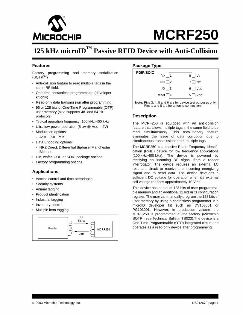
2003 Microchip Technology Inc. DS21267F-page 1 MCRF250 Features Factory programming and memory serialization (SQTP SM ) • Anti-collision feature to read multiple tags in the same RF field. • One-time contactless programmable (developer kit only) • Read-only data transmission after programming • 96 or 128 bits of One-Time Programmable (OTP) user memory (also supports 48- and 64-bit protocols) • Typical operation frequency: 100 kHz-400 kHz • Ultra low-power operation (5 µA @ VCC = 2V) • Modulation options: - ASK, FSK, PSK • Data Encoding options: - NRZ Direct, Differential Biphase, Manchester Biphase • Die, wafer, COB or SOIC package options • Factory programming options Applications • Access control and time attendance • Security systems • Animal tagging • Product identification • Industrial tagging • Inventory control • Multiple item tagging Package Type Description The MCRF250 is equipped with an anti-collision feature that allows multiple tags in the same field to be read simultaneously. This revolutionary feature eliminates the issue of data corruption due to simultaneous transmissions from multiple tags. The MCRF250 is a passive Radio Frequency Identifi- cation (RFID) device for low frequency applications (100 kHz-400 kHz). The device is powered by rectifying an incoming RF signal from a reader interrogator. The device requires an external LC resonant circuit to receive the incoming energizing signal and to send data. The device develops a sufficient DC voltage for operation when it’s external coil voltage reaches approximately 10 VPP. This device has a total of 128 bits of user programma- ble memory and an additional 12 bits in its configuration register. The user can manually program the 128 bits of user memory by using a contactless programmer in a microID developer kit such as DV103001 or PG103001. However, in production volume the MCRF250 is programmed at the factory (Microchip SQTP - see Technical Bulletin TB023).The device is a One-Time Programmable (OTP) integrated circuit and operates as a read-only device after programming. MCRF250 Reader RF Signal Data PDIP/SOIC VA VB 1 2 3 4 8 7 6 5 NC I/O Reset NC VSS VCC Note: Pins 3, 4, 5 and 6 are for device test purposes only. Pins 1 and 8 are for antenna connection. 125 kHz microID ™ Passive RFID Device with Anti-Collision
Transcript of MCRF250 125 kHz microID™ Passive RFID Device with...
MCRF250125 kHz microID™ Passive RFID Device with Anti-Collision
Features
Factory programming and memory serialization(SQTPSM)
• Anti-collision feature to read multiple tags in the same RF field.
• One-time contactless programmable (developer kit only)
• Read-only data transmission after programming• 96 or 128 bits of One-Time Programmable (OTP)
user memory (also supports 48- and 64-bit protocols)
• Typical operation frequency: 100 kHz-400 kHz• Ultra low-power operation (5 µA @ VCC = 2V)
• Modulation options:- ASK, FSK, PSK
• Data Encoding options:
- NRZ Direct, Differential Biphase, Manchester Biphase
• Die, wafer, COB or SOIC package options• Factory programming options
Applications
• Access control and time attendance• Security systems
• Animal tagging• Product identification• Industrial tagging
• Inventory control• Multiple item tagging
Package Type
Description
The MCRF250 is equipped with an anti-collisionfeature that allows multiple tags in the same field to beread simultaneously. This revolutionary featureeliminates the issue of data corruption due tosimultaneous transmissions from multiple tags.
The MCRF250 is a passive Radio Frequency Identifi-cation (RFID) device for low frequency applications(100 kHz-400 kHz). The device is powered byrectifying an incoming RF signal from a readerinterrogator. The device requires an external LCresonant circuit to receive the incoming energizingsignal and to send data. The device develops asufficient DC voltage for operation when it’s externalcoil voltage reaches approximately 10 VPP.
This device has a total of 128 bits of user programma-ble memory and an additional 12 bits in its configurationregister. The user can manually program the 128 bits ofuser memory by using a contactless programmer in amicroID developer kit such as DV103001 orPG103001. However, in production volume theMCRF250 is programmed at the factory (MicrochipSQTP - see Technical Bulletin TB023).The device is aOne-Time Programmable (OTP) integrated circuit andoperates as a read-only device after programming.
MCRF250Reader
RFSignal
Data
PDIP/SOICVA VB1
2
3
4
8
7
6
5
NC
I/O
Reset
NC
VSS
VCC
Note: Pins 3, 4, 5 and 6 are for device test purposes only.Pins 1 and 8 are for antenna connection.
2003 Microchip Technology Inc. DS21267F-page 1
MCRF250
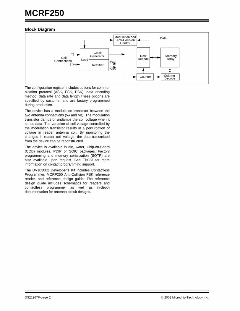
Block Diagram
The configuration register includes options for commu-nication protocol (ASK, FSK, PSK), data encodingmethod, data rate and data length.These options arespecified by customer and are factory programmedduring production.
The device has a modulation transistor between thetwo antenna connections (VA and VB). The modulationtransistor damps or undamps the coil voltage when itsends data. The variation of coil voltage controlled bythe modulation transistor results in a perturbation ofvoltage in reader antenna coil. By monitoring thechanges in reader coil voltage, the data transmittedfrom the device can be reconstructed.
The device is available in die, wafer, Chip-on-Board(COB) modules, PDIP or SOIC packages. Factoryprogramming and memory serialization (SQTP) arealso available upon request. See TB023 for moreinformation on contact programming support.
The DV103002 Developer’s Kit includes ContactlessProgrammer, MCRF250 Anti-Collision FSK referencereader, and reference design guide. The referencedesign guide includes schematics for readers andcontactless programmer as well as in-depthdocumentation for antenna circuit designs.
Column
Memory Array
VCC
VSS
Rectifier
ClockGenerator
CoilConnections
Decode
RowDecode
Modulation and Anti-Collision
Counter
Data
Load
Control
DS21267F-page 2 2003 Microchip Technology Inc.
MCRF250
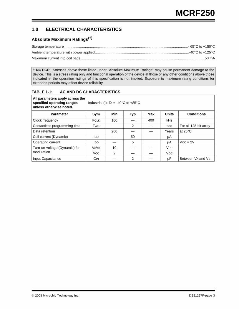
1.0 ELECTRICAL CHARACTERISTICS
Absolute Maximum Ratings(†)
Storage temperature .............................................................................................................................. - 65°C to +150°C
Ambient temperature with power applied................................................................................................-40°C to +125°C
Maximum current into coil pads ..............................................................................................................................50 mA
TABLE 1-1: AC AND DC CHARACTERISTICS
† NOTICE: Stresses above those listed under "Absolute Maximum Ratings" may cause permanent damage to thedevice. This is a stress rating only and functional operation of the device at those or any other conditions above thoseindicated in the operation listings of this specification is not implied. Exposure to maximum rating conditions forextended periods may affect device reliability.
All parameters apply across the specified operating ranges unless otherwise noted.
Industrial (I): TA = -40°C to +85°C
Parameter Sym Min Typ Max Units Conditions
Clock frequency FCLK 100 — 400 kHz
Contactless programming time TWC — 2 — sec For all 128-bit array
Data retention 200 — — Years at 25°C
Coil current (Dynamic) ICD — 50 µA
Operating current IDD — 5 µA VCC = 2V
Turn-on-voltage (Dynamic) for modulation
VAVB 10 — — VPP
VCC 2 — — VDC
Input Capacitance CIN — 2 — pF Between VA and VB
2003 Microchip Technology Inc. DS21267F-page 3
MCRF250
2.0 FUNCTIONAL DESCRIPTION
The device contains three major building blocks. Theyare RF front-end, configuration and control logic, andmemory sections. The Block Diagram is shown onpage 1.
2.1 RF Front-End
The RF front-end of the device includes circuits forrectification of the carrier, VDD (operating voltage), andhigh-voltage clamping to prevent excessive voltagefrom being applied to the device. This section alsogenerates a system clock from the incoming carriersignal and modulates the carrier signal to transmit datato the reader.
2.1.1 RECTIFIER – AC CLAMP
The rectifier circuit rectifies RF voltage on the externalLC antenna circuit. Any excessive voltage on the tunedcircuit is clamped by the internal circuitry to a safe levelto prevent damage to the IC.
2.1.2 POWER-ON RESET
This circuit generates a Power-on Reset when the tagfirst enters the reader field. The Reset releases whensufficient power has developed on the VDD regulator toallow correct operation.
2.1.3 CLOCK GENERATOR
This circuit generates a clock based on the carrierfrequency from the reader. This clock is used to deriveall timing in the device, including the baud rate andmodulation rate.
2.1.4 IRQ DETECTOR
This circuitry detects an interrupt in the continuouselectromagnetic field of the interrogator. An IRQ(interrupt request) is defined as the absence of theelectromagnetic field for a specific number of clockcycles. Detection of an IRQ will trigger the device toenter the Anti-collision mode. This mode is discussedin detail in Section 5.0 “Anti-Collision”.
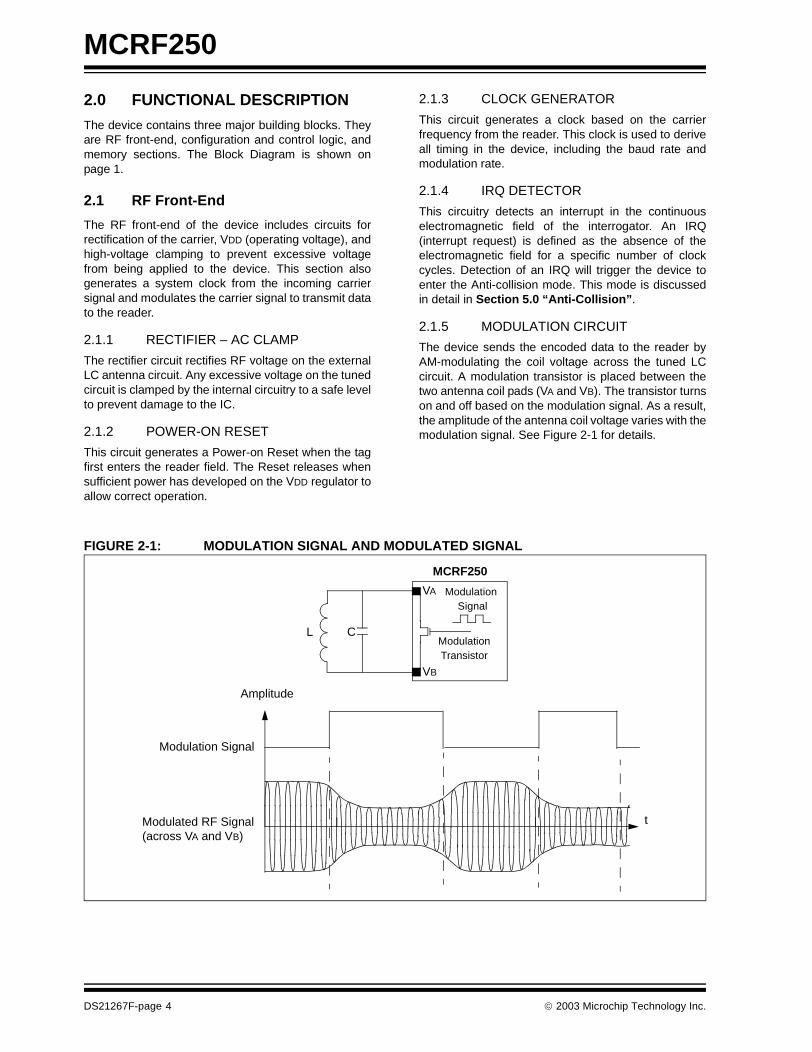
2.1.5 MODULATION CIRCUIT
The device sends the encoded data to the reader byAM-modulating the coil voltage across the tuned LCcircuit. A modulation transistor is placed between thetwo antenna coil pads (VA and VB). The transistor turnson and off based on the modulation signal. As a result,the amplitude of the antenna coil voltage varies with themodulation signal. See Figure 2-1 for details.
FIGURE 2-1: MODULATION SIGNAL AND MODULATED SIGNAL
MCRF250
Modulation Signal
VA
VB
Modulation
Modulation Signal
Modulated RF Signal(across VA and VB)
L C
Amplitude
t
Transistor
DS21267F-page 4 2003 Microchip Technology Inc.

MCRF250
2.2 Configuration Register and Control Logic
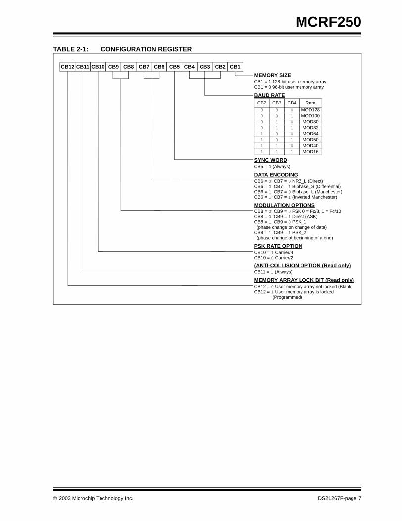
The configuration register determines the operationalparameters of the device. The configuration registercan not be programmed contactlessly; it isprogrammed during wafer probe at the Microchip fac-tory. CB11 is always a one; CB12 is set when success-ful contact or contactless programming of the dataarray has been completed. Once CB12 is set, deviceprogramming and erasing is disabled. Table 2-1contains a description of the bit functions of the controlregister.
2.2.1 BAUD RATE TIMING OPTION
The chip will access data at a baud rate determined bybits CB2, CB3, and CB4 of the configuration register.For example, MOD32 (CB2 = 0, CB3 = 1, CB4 = 1) has32 RF cycles per bit. This gives the data rate of 4 kHzfor the RF carrier frequency of 128 kHz.
The default timing is MOD 128 (FCLK/128), and thismode is used for contact and contactless program-ming. Once the array is successfully programmed, thelock bit CB12 is set. When the lock bit is set, program-ming and erasing the device becomes permanentlydisabled. The configuration register has no effect ondevice timing until the EEPROM data array isprogrammed (CB12 = 1).
2.2.2 DATA ENCODING OPTION
This logic acts upon the serial data being read from theEEPROM. The logic encodes the data according to theconfiguration bits CB6 and CB7. CB6 and CB7determine the data encoding method. The availablechoices are:
• Non-return to zero-level (NRZ_L)• Biphase_S (Differential)• Biphase_L (Manchester)
• Inverted Manchester
2.2.3 MODULATION OPTION
CB8 and CB9 determine the modulation protocol of theencoded data. The available choices are:
• ASK• FSK
• PSK_1• PSK_2
When ASK (direct) option is chosen, the encoded datais fed into the modulation transistor without change.
When FSK option is chosen, the encoded data isrepresented by:
a) Sets of 10 RF carrier cycles (first 5 cycles →higher amplitude, the last 5 cycles → loweramplitude) for logic “high” level.
b) Sets of 8 RF carrier cycles (first 4 cycles →higher amplitude, the last 4 cycles → loweramplitude) for logic “low” level.
For example, FSK signal for MOD40 is represented:
a) 4 sets of 10 RF carrier cycles for data ‘1’.
b) 5 sets of 8 RF carrier cycles for data ‘0’.
Refer to Figure 2-2 for the FSK signal with MOD40option.
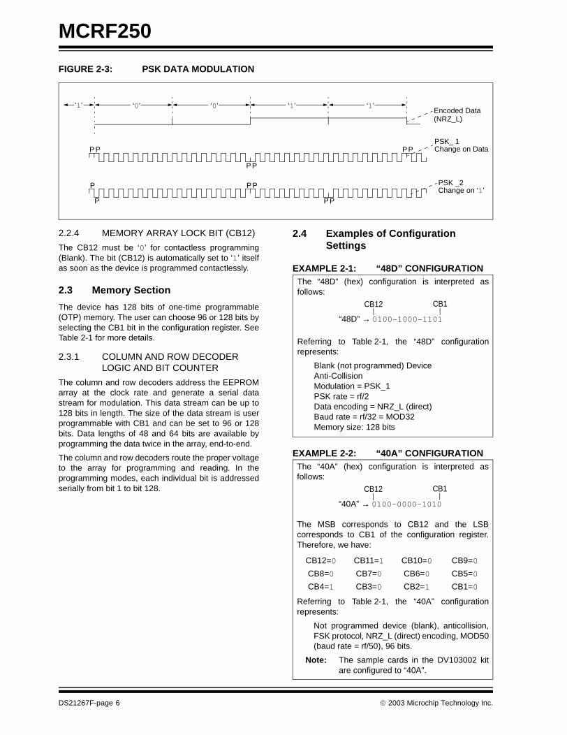
The PSK_1 represents change in the phase of themodulation signal at the change of the encoded data.For example, the phase changes when the encodeddata is changed from ‘1’ to ‘0’, or from ‘0’ to ‘1’.
The PSK_2 represents change in the phase at thechange on ‘1’. For example, the phase changes whenthe encoded data is changed from ‘0’ to ‘1’, or from ‘1’to ‘1’.
FIGURE 2-2: ENCODED DATA AND FSK OUTPUT SIGNAL FOR MOD40 OPTION
Encoded Data ‘1’ Encoded Data ‘0’
40 RF cycles 40 RF cycles
5 cycles (HI)
5 cycles (LO)4 cycles (HI)
4 cycles (LO)
2003 Microchip Technology Inc. DS21267F-page 5
MCRF250
FIGURE 2-3: PSK DATA MODULATION
2.2.4 MEMORY ARRAY LOCK BIT (CB12)
The CB12 must be ‘0’ for contactless programming(Blank). The bit (CB12) is automatically set to ‘1’ itselfas soon as the device is programmed contactlessly.
2.3 Memory Section
The device has 128 bits of one-time programmable(OTP) memory. The user can choose 96 or 128 bits byselecting the CB1 bit in the configuration register. SeeTable 2-1 for more details.
2.3.1 COLUMN AND ROW DECODER LOGIC AND BIT COUNTER
The column and row decoders address the EEPROMarray at the clock rate and generate a serial datastream for modulation. This data stream can be up to128 bits in length. The size of the data stream is userprogrammable with CB1 and can be set to 96 or 128bits. Data lengths of 48 and 64 bits are available byprogramming the data twice in the array, end-to-end.
The column and row decoders route the proper voltageto the array for programming and reading. In theprogramming modes, each individual bit is addressedserially from bit 1 to bit 128.
2.4 Examples of Configuration Settings
EXAMPLE 2-1: “48D” CONFIGURATION
EXAMPLE 2-2: “40A” CONFIGURATION
P
P
P P
PP
PP
PP
PP
‘0’ ‘0’ ‘1’‘1’Encoded Data
PSK_ 1Change on Data
PSK _2Change on ‘1’
(NRZ_L)
‘1’
The “48D” (hex) configuration is interpreted asfollows:
Referring to Table 2-1, the “48D” configurationrepresents:
Blank (not programmed) DeviceAnti-CollisionModulation = PSK_1PSK rate = rf/2Data encoding = NRZ_L (direct)Baud rate = rf/32 = MOD32Memory size: 128 bits
“48D” → 0100-1000-1101
CB12 CB1
The “40A” (hex) configuration is interpreted asfollows:
The MSB corresponds to CB12 and the LSBcorresponds to CB1 of the configuration register.Therefore, we have:
Referring to Table 2-1, the “40A” configurationrepresents:
Not programmed device (blank), anticollision,FSK protocol, NRZ_L (direct) encoding, MOD50(baud rate = rf/50), 96 bits.
Note: The sample cards in the DV103002 kitare configured to “40A”.
CB12=0 CB11=1 CB10=0 CB9=0
CB8=0 CB7=0 CB6=0 CB5=0
CB4=1 CB3=0 CB2=1 CB1=0
“40A” → 0100-0000-1010
CB12 CB1
DS21267F-page 6 2003 Microchip Technology Inc.
MCRF250
TABLE 2-1: CONFIGURATION REGISTER
CB12 CB11 CB10 CB9 CB8 CB7 CB6 CB5 CB4 CB3 CB2 CB1
MEMORY SIZECB1 = 1 128-bit user memory arrayCB1 = 0 96-bit user memory array
BAUD RATE
SYNC WORDCB5 = 0 (Always)
DATA ENCODINGCB6 = 0; CB7 = 0 NRZ_L (Direct)CB6 = 0; CB7 = 1 Biphase_S (Differential)CB6 = 1; CB7 = 0 Biphase_L (Manchester)CB6 = 1; CB7 = 1 (Inverted Manchester)
MODULATION OPTIONSCB8 = 0; CB9 = 0 FSK 0 = Fc/8, 1 = Fc/10CB8 = 0; CB9 = 1 Direct (ASK)CB8 = 1; CB9 = 0 PSK_1(phase change on change of data)
CB8 = 1; CB9 = 1 PSK_2(phase change at beginning of a one)
PSK RATE OPTIONCB10 = 1 Carrier/4CB10 = 0 Carrier/2
(ANTI-COLLISION OPTION (Read only)CB11 = 1 (Always)
MEMORY ARRAY LOCK BIT (Read only)CB12 = 0 User memory array not locked (Blank)CB12 = 1 User memory array is locked
(Programmed)
CB2 CB3 CB4 Rate
0 0 0 MOD1280 0 1 MOD1000 1 0 MOD800 1 1 MOD321 0 0 MOD641 0 1 MOD501 1 0 MOD401 1 1 MOD16
2003 Microchip Technology Inc. DS21267F-page 7
MCRF250
3.0 MODES OF OPERATION
The device has two basic modes of operation: NativeMode and Read Mode.
3.1 Native Mode
Every unprogrammed blank device (CB12 = 0)operates in Native mode, regardless of configurationregister settings:
Baud rate = FCLK/128, FSK, NRZ_L (direct)
Once the user memory is programmed, the lock bit isset (CB12 = 1) which causes the MCRF250 to switchfrom Native mode to Communication mode defined bythe configuration register.
Refer to Figure 4-1 for contactless programmingsequence. Also see the microID™ 125 kHz RFIDSystem Design Guide (DS51115) for more information.
3.2 Read Mode
After the device is programmed (CB12 = 1), the deviceis operated in the Read-only mode. The devicetransmits its data according to the protocol in theconfiguration register.
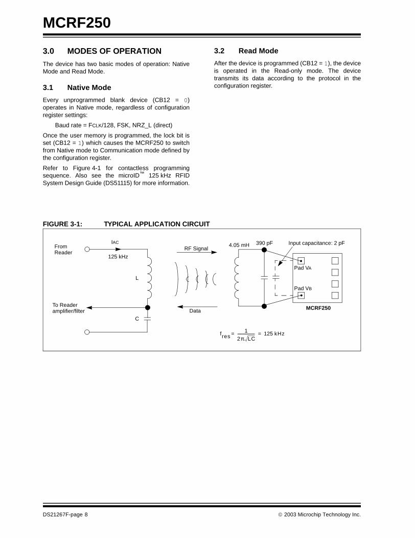
FIGURE 3-1: TYPICAL APPLICATION CIRCUIT
Pad VB
Pad VA
Input capacitance: 2 pFRF Signal
Data
C
To Readeramplifier/filter
From Reader
IAC
L
4.05 mH 390 pF
fres1
2π LC------------------- 125 kHz= =
125 kHz
MCRF250
DS21267F-page 8 2003 Microchip Technology Inc.
MCRF250
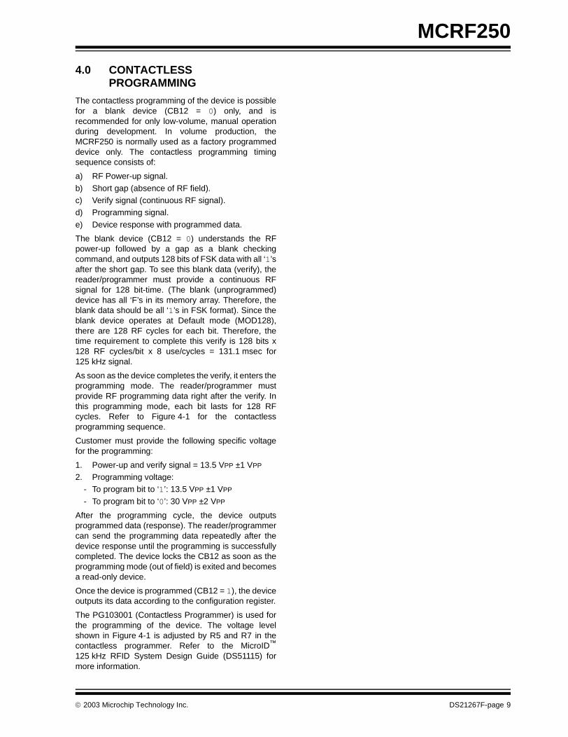
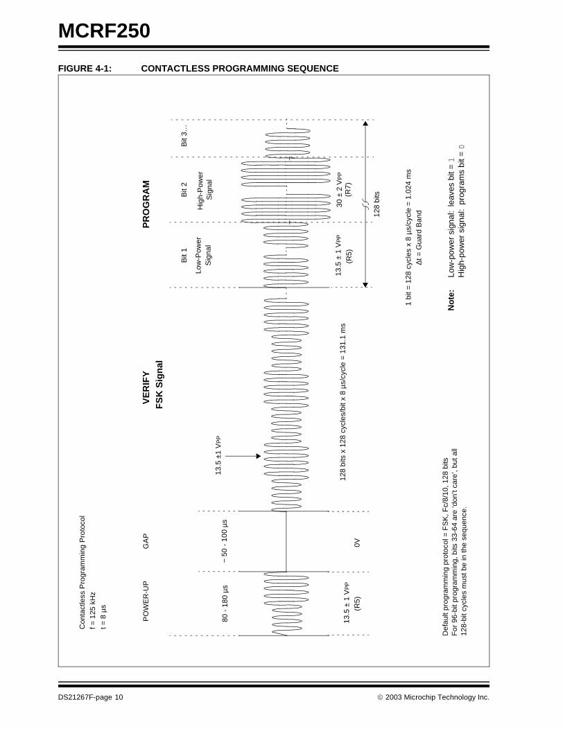
4.0 CONTACTLESS PROGRAMMING
The contactless programming of the device is possiblefor a blank device (CB12 = 0) only, and isrecommended for only low-volume, manual operationduring development. In volume production, theMCRF250 is normally used as a factory programmeddevice only. The contactless programming timingsequence consists of:
a) RF Power-up signal.
b) Short gap (absence of RF field).c) Verify signal (continuous RF signal).d) Programming signal.
e) Device response with programmed data.
The blank device (CB12 = 0) understands the RFpower-up followed by a gap as a blank checkingcommand, and outputs 128 bits of FSK data with all ‘1’safter the short gap. To see this blank data (verify), thereader/programmer must provide a continuous RFsignal for 128 bit-time. (The blank (unprogrammed)device has all ‘F’s in its memory array. Therefore, theblank data should be all ‘1’s in FSK format). Since theblank device operates at Default mode (MOD128),there are 128 RF cycles for each bit. Therefore, thetime requirement to complete this verify is 128 bits x128 RF cycles/bit x 8 use/cycles = 131.1 msec for125 kHz signal.
As soon as the device completes the verify, it enters theprogramming mode. The reader/programmer mustprovide RF programming data right after the verify. Inthis programming mode, each bit lasts for 128 RFcycles. Refer to Figure 4-1 for the contactlessprogramming sequence.
Customer must provide the following specific voltagefor the programming:
1. Power-up and verify signal = 13.5 VPP ±1 VPP
2. Programming voltage:- To program bit to ‘1’: 13.5 VPP ±1 VPP
- To program bit to ‘0’: 30 VPP ±2 VPP
After the programming cycle, the device outputsprogrammed data (response). The reader/programmercan send the programming data repeatedly after thedevice response until the programming is successfullycompleted. The device locks the CB12 as soon as theprogramming mode (out of field) is exited and becomesa read-only device.
Once the device is programmed (CB12 = 1), the deviceoutputs its data according to the configuration register.
The PG103001 (Contactless Programmer) is used forthe programming of the device. The voltage levelshown in Figure 4-1 is adjusted by R5 and R7 in thecontactless programmer. Refer to the MicroID™
125 kHz RFID System Design Guide (DS51115) formore information.
2003 Microchip Technology Inc. DS21267F-page 9
MCRF250
FIGURE 4-1: CONTACTLESS PROGRAMMING SEQUENCE
PO
WE
R-U
PG
AP
~ 5
0 -
100
µs13
.5 ±
1 V
PP
Hig
h-P
ower
30 ±
2 V
PP
Bit
1B
it 2
128
bits
x 1
28 c
ycle
s/bi
t x 8
µs/c
ycle
= 1
31.1
ms
13.5
± 1
VP
P
Con
tact
less
Pro
gram
min
g P
roto
col
f = 1
25 k
Hz
t = 8
µs
Bit
3…
PR
OG
RA
M
1 bi
t = 1
28 c
ycle
s x
8µs
/cyc
le =
1.0
24m
s
80 -
180
µs
VE
RIF
YF
SK
Sig
nal
(R5)
128
bits
∆t =
Gua
rd B
and
0V
13.5
± 1
VP
P
(R5)
Low
-Pow
erS
igna
lS
igna
l
(R7)
No
te:
Low
-pow
er s
igna
l:le
aves
bit
= 1
Hig
h-po
wer
sig
nal:
prog
ram
s bi
t = 0
Def
ault
prog
ram
min
g pr
otoc
ol =
FS
K, F
c/8/
10, 1
28 b
itsF
or 9
6-bi
t pro
gram
min
g, b
its 3
3-64
are
‘don
’t ca
re’,
but a
ll 12
8-bi
t cyc
les
mus
t be
in th
e se
quen
ce.
DS21267F-page 10 2003 Microchip Technology Inc.

MCRF250
5.0 ANTI-COLLISION
The anti-collision feature is enabled after the array lockbit (CB12) is set. This feature relies on internal randomnumber oscillator/counter and special gap pulses(= turn off RF field) provided by a reader. Figure 5-1shows the anti-collision flowchart.
The MCRF250 works with the following anti-collisionfeatures:
1. The device does not output data until it sees thefirst gap. (no RF field for about 60 µsec.)
2. When the device sees the first gap, the internalrandom number oscillator starts clockingimmediately after the gap.
3. At the same time, the internal random numbercounter starts counting the random numberclocks.
4. The device waits for 5 bit times (about 5 msec.for MOD128 configuration).
Example: 1 bit time=RF/128=1 msec for 128 kHzfor MOD128
5. After the 5 bit times, the device sends data.6. At this time, the random number counter is still
running. If multiple tags in the field send data atthe same time, the reader will see a datacollision.
7. When the reader sees the data collision, it sendsthe second gap pulse. (no RF field for about60 µsec.)
8. After the second gap pulse, there is a chancethat the random number counter of each tagmay have a different value due to a randomvariation in the oscillator’s starting time, etc.
9. After the second gap, the random numberoscillator stops and the random number counterwill decrement at each subsequent gap.
10. The device will transmit data when its randomnumber counter reaches ‘0’.
11. The device repeats this sequence (as shown inthe flowchart in Figure 5-1) according to theproper gap pulses provided by the reader.
FIGURE 5-1: ANTI-COLLISION FLOWCHART
Note: Each device will output data indifferent time frames since eachrandom number counter will arrive at‘0’ at different times. As a result, thereader can receive clean data from adifferent tag in each time frame.
Begin
Provide Gap*
Wait 5-bit times
Is
Read Tag
Isonly one tagmodulating?
modulationpresent?
Provide gap in thefirst half of the firstbit time to make
tag stop transmitting
No
No
Yes
Yes
Note: *Gap = lack of RF carrier signal = 60 µs ± 20%.
2003 Microchip Technology Inc. DS21267F-page 11
MCRF250
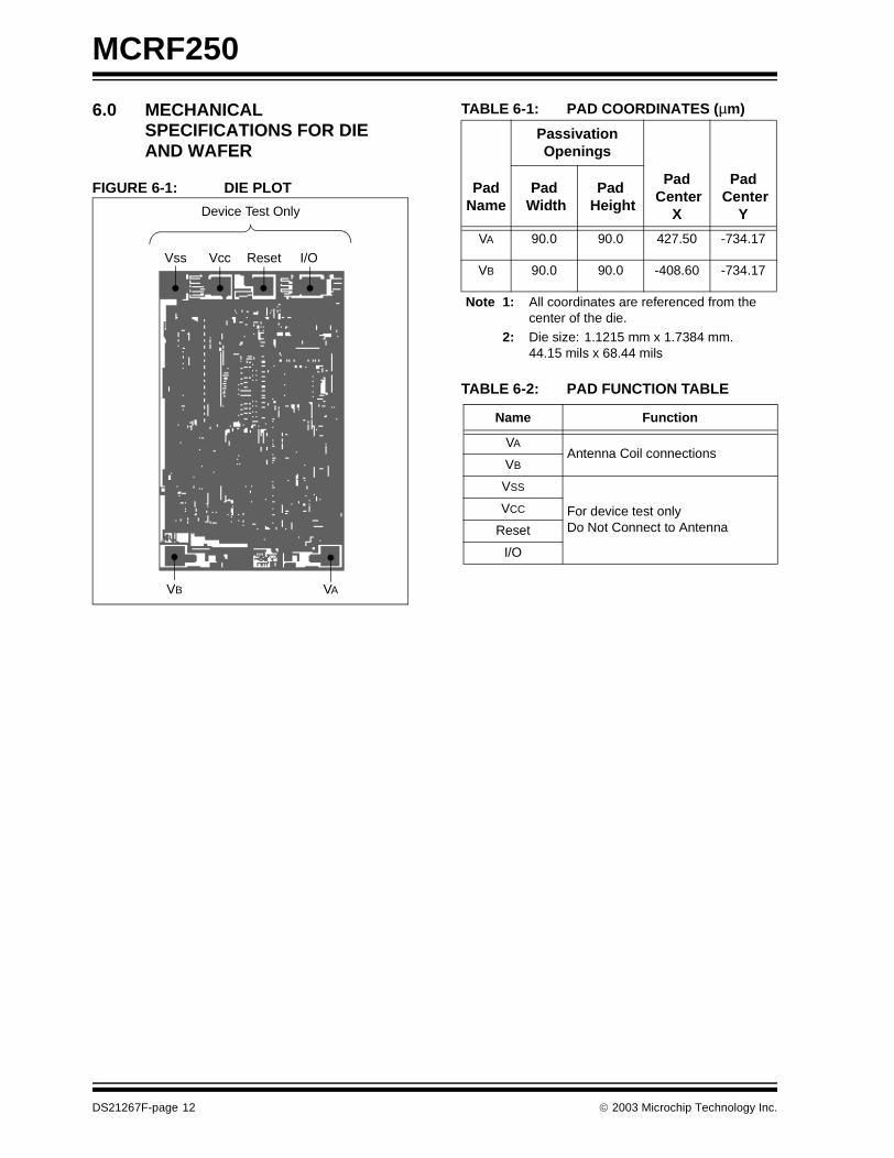
6.0 MECHANICAL SPECIFICATIONS FOR DIE AND WAFER
FIGURE 6-1: DIE PLOT
TABLE 6-1: PAD COORDINATES (µm)
TABLE 6-2: PAD FUNCTION TABLE
VB VA
Vss Vcc I/OReset
Device Test Only
Passivation Openings
PadName
Pad Width
Pad Height
Pad Center
X
Pad Center
Y
VA 90.0 90.0 427.50 -734.17
VB 90.0 90.0 -408.60 -734.17
Note 1: All coordinates are referenced from the center of the die.
2: Die size: 1.1215 mm x 1.7384 mm.44.15 mils x 68.44 mils
Name Function
VAAntenna Coil connections
VB
VSS
For device test onlyDo Not Connect to Antenna
VCC
Reset
I/O
DS21267F-page 12 2003 Microchip Technology Inc.
MCRF250
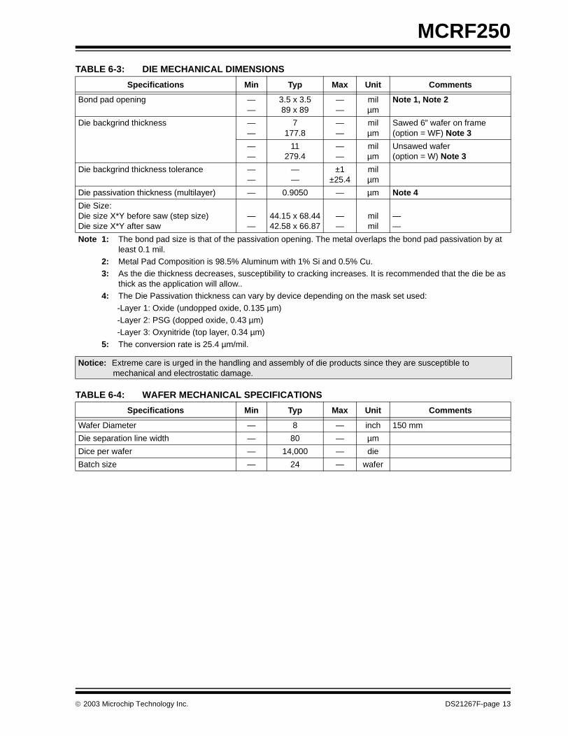
TABLE 6-3: DIE MECHANICAL DIMENSIONS
TABLE 6-4: WAFER MECHANICAL SPECIFICATIONS
Specifications Min Typ Max Unit Comments
Bond pad opening ——
3.5 x 3.589 x 89
——
milµm
Note 1, Note 2
Die backgrind thickness ——
7177.8
——
milµm
Sawed 6” wafer on frame (option = WF) Note 3
——
11279.4
——
milµm
Unsawed wafer(option = W) Note 3
Die backgrind thickness tolerance ——
——
±1±25.4
milµm
Die passivation thickness (multilayer) — 0.9050 — µm Note 4
Die Size:Die size X*Y before saw (step size)Die size X*Y after saw
——
44.15 x 68.4442.58 x 66.87
——
milmil
——
Note 1: The bond pad size is that of the passivation opening. The metal overlaps the bond pad passivation by at least 0.1 mil.
2: Metal Pad Composition is 98.5% Aluminum with 1% Si and 0.5% Cu.3: As the die thickness decreases, susceptibility to cracking increases. It is recommended that the die be as
thick as the application will allow..4: The Die Passivation thickness can vary by device depending on the mask set used:
-Layer 1: Oxide (undopped oxide, 0.135 µm)-Layer 2: PSG (dopped oxide, 0.43 µm)-Layer 3: Oxynitride (top layer, 0.34 µm)
5: The conversion rate is 25.4 µm/mil.
Notice: Extreme care is urged in the handling and assembly of die products since they are susceptible to mechanical and electrostatic damage.
Specifications Min Typ Max Unit Comments
Wafer Diameter — 8 — inch 150 mm
Die separation line width — 80 — µm
Dice per wafer — 14,000 — die
Batch size — 24 — wafer
2003 Microchip Technology Inc. DS21267F-page 13
MCRF250
7.0 FAILED DIE IDENTIFICATION
Every die on the wafer is electrically tested accordingto the data sheet specifications and visually inspectedto detect any mechanical damage such as mechanicalcracks and scratches.
Any failed die in the test or visual inspection is identifiedby black colored inking. Therefore, any die coveredwith black ink should not be used.
The ink dot specification:
• Ink dot size: minimum 20 µm x 20 µm• Position: central third of die
• Color: black
8.0 WAFER DELIVERY DOCUMENTATION
Each wafer container is marked with the followinginformation:
• Microchip Technology Inc. MP Code• Lot Number
• Total number of wafer in the container• Total number of good dice in the container• Average die per wafer (DPW)
• Scribe number of wafer with number of good dice.
9.0 NOTICE ON DIE AND WAFER HANDLING
The device is very susceptible to ElectrostaticDischarge (ESD). ESD can cause critical damage tothe device. Special attention is needed during thehandling process.
Any ultraviolet (UV) light can erase the memory cellcontents of an unpackaged device. Fluorescent lightsand sun light can also erase the memory cell althoughit takes more time than UV lamps. Therefore, keep anyunpackaged devices out of UV light and also avoiddirect exposure from strong fluorescent lights and sunlight.
Certain integrated circuit (IC) manufacturing, chip-on-board (COB) and tag assembly operations may use UVlight. Operations such as backgrind, de-tape, certaincleaning operations, epoxy or glue cure should be donewithout exposing the die surface to UV light.
Using x-ray for die inspection will not harm the die, norerase memory cell contents.
DS21267F-page 14 2003 Microchip Technology Inc.
MCRF250
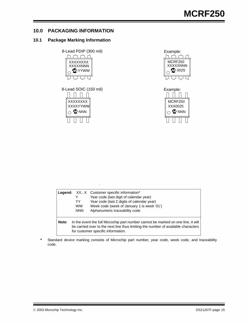
10.0 PACKAGING INFORMATION
10.1 Package Marking Information
XXXXXXXXXXXXXNNN
YYWW
8-Lead PDIP (300 mil) Example:
8-Lead SOIC (150 mil) Example:
XXXXXXXXXXXXYYWW
NNN
MCRF250XXXXXNNN
0025
Legend: XX...X Customer specific information*Y Year code (last digit of calendar year)YY Year code (last 2 digits of calendar year)WW Week code (week of January 1 is week ‘01’)NNN Alphanumeric traceability code
Note: In the event the full Microchip part number cannot be marked on one line, it willbe carried over to the next line thus limiting the number of available charactersfor customer specific information.
* Standard device marking consists of Microchip part number, year code, week code, and traceabilitycode.
MCRF250XXX0025
NNN
2003 Microchip Technology Inc. DS21267F-page 15
MCRF250
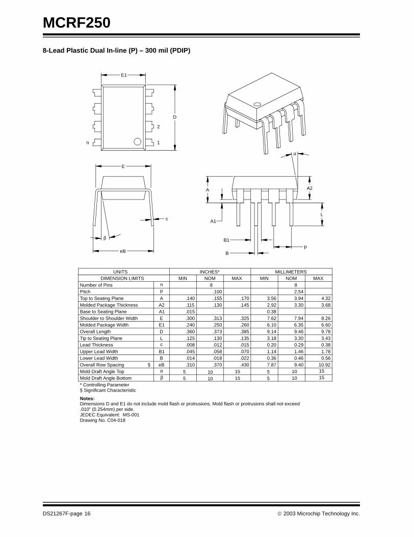
8-Lead Plastic Dual In-line (P) – 300 mil (PDIP)
B1
B
A1
A
L
A2
p
α
E
eB
β
c
E1
n
D
1
2
UNITS INCHES* MILLIMETERSDIMENSION LIMITS MIN NOM MAX MIN NOM MAX
Number of Pins n 8 8Pitch p .100 2.54Top to Seating Plane A .140 .155 .170 3.56 3.94 4.32Molded Package Thickness A2 .115 .130 .145 2.92 3.30 3.68Base to Seating Plane A1 .015 0.38Shoulder to Shoulder Width E .300 .313 .325 7.62 7.94 8.26Molded Package Width E1 .240 .250 .260 6.10 6.35 6.60Overall Length D .360 .373 .385 9.14 9.46 9.78Tip to Seating Plane L .125 .130 .135 3.18 3.30 3.43Lead Thickness c .008 .012 .015 0.20 0.29 0.38Upper Lead Width B1 .045 .058 .070 1.14 1.46 1.78Lower Lead Width B .014 .018 .022 0.36 0.46 0.56Overall Row Spacing § eB .310 .370 .430 7.87 9.40 10.92Mold Draft Angle Top α 5 10 15 5 10 15
Mold Draft Angle Bottom β 5 10 15 5 10 15
* Controlling Parameter
Notes:Dimensions D and E1 do not include mold flash or protrusions. Mold flash or protrusions shall not exceed
JEDEC Equivalent: MS-001Drawing No. C04-018
.010” (0.254mm) per side.
§ Significant Characteristic
DS21267F-page 16 2003 Microchip Technology Inc.
MCRF250
8-Lead Plastic Small Outline (SN) – Narrow, 150 mil (SOIC)
Foot Angle φ 0 4 8 0 4 8
1512015120βMold Draft Angle Bottom
1512015120αMold Draft Angle Top
.51.42.33.020.017.013BLead Width
.25.23.20.010.009.008cLead Thickness
.76.62.48.030.025.019LFoot Length
.51.38.25.020.015.010hChamfer Distance
5.004.904.80.197.193.189DOverall Length
3.993.913.71.157.154.146E1Molded Package Width
6.206.025.79.244.237.228EOverall Width
.25.18.10.010.007.004A1Standoff §
1.551.421.32.061.056.052A2Molded Package Thickness
1.751.551.35.069.061.053AOverall Height1.27.050pPitch
88nNumber of PinsMAXNOMMINMAXNOMMINDIMENSION LIMITS
MILLIMETERSINCHES*UNITS
2
1
D
n
p
B
E
E1
h
Lβ
c
45°
φ
A2
α
A
A1
* Controlling Parameter
Notes:Dimensions D and E1 do not include mold flash or protrusions. Mold flash or protrusions shall not exceed .010” (0.254mm) per side.JEDEC Equivalent: MS-012Drawing No. C04-057
§ Significant Characteristic
2003 Microchip Technology Inc. DS21267F-page 17
MCRF250
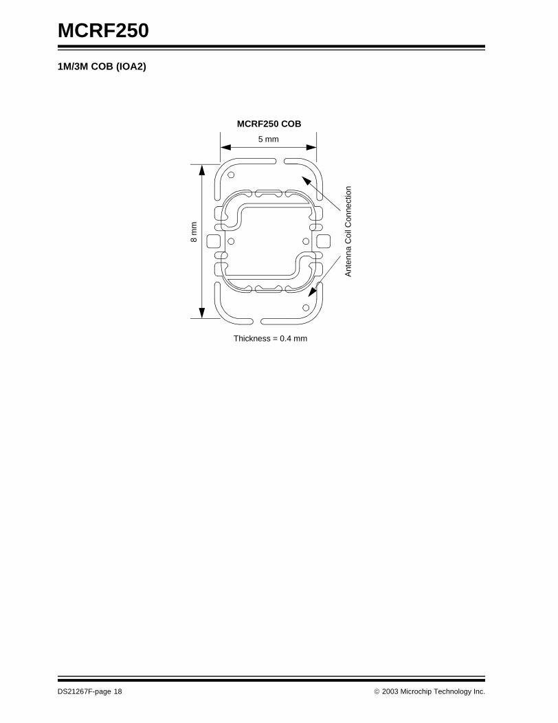
1M/3M COB (IOA2)
5 mm
8m
m
Thickness = 0.4 mmA
nten
na C
oil C
onne
ctio
n
MCRF250 COB
DS21267F-page 18 2003 Microchip Technology Inc.

MCRF250
ON-LINE SUPPORT
Microchip provides on-line support on the MicrochipWorld Wide Web site.
The web site is used by Microchip as a means to makefiles and information easily available to customers. Toview the site, the user must have access to the Internetand a web browser, such as Netscape® or Microsoft®
Internet Explorer. Files are also available for FTPdownload from our FTP site.
Connecting to the Microchip Internet Web Site
The Microchip web site is available at the followingURL:
www.microchip.com
The file transfer site is available by using an FTPservice to connect to:
ftp://ftp.microchip.com
The web site and file transfer site provide a variety ofservices. Users may download files for the latestDevelopment Tools, Data Sheets, Application Notes,User's Guides, Articles and Sample Programs. Avariety of Microchip specific business information isalso available, including listings of Microchip salesoffices, distributors and factory representatives. Otherdata available for consideration is:
• Latest Microchip Press Releases• Technical Support Section with Frequently Asked
Questions • Design Tips
• Device Errata• Job Postings• Microchip Consultant Program Member Listing
• Links to other useful web sites related to Microchip Products
• Conferences for products, Development Systems, technical information and more
• Listing of seminars and events
SYSTEMS INFORMATION AND UPGRADE HOT LINE
The Systems Information and Upgrade Line providessystem users a listing of the latest versions of all ofMicrochip's development systems software products.Plus, this line provides information on how customerscan receive the most current upgrade kits. The Hot LineNumbers are:
1-800-755-2345 for U.S. and most of Canada, and
1-480-792-7302 for the rest of the world.
042003
2003 Microchip Technology Inc. DS21267F-page 19

MCRF250
READER RESPONSE
It is our intention to provide you with the best documentation possible to ensure successful use of your Microchip prod-uct. If you wish to provide your comments on organization, clarity, subject matter, and ways in which our documentationcan better serve you, please FAX your comments to the Technical Publications Manager at (480) 792-4150.
Please list the following information, and use this outline to provide us with your comments about this document.
To: Technical Publications Manager
RE: Reader Response
Total Pages Sent ________
From: Name
Company
Address
City / State / ZIP / Country
Telephone: (_______) _________ - _________
Application (optional):
Would you like a reply? Y N
Device: Literature Number:
Questions:
FAX: (______) _________ - _________
DS21267FMCRF250
1. What are the best features of this document?
2. How does this document meet your hardware and software development needs?
3. Do you find the organization of this document easy to follow? If not, why?
4. What additions to the document do you think would enhance the structure and subject?
5. What deletions from the document could be made without affecting the overall usefulness?
6. Is there any incorrect or misleading information (what and where)?
7. How would you improve this document?
DS21267F-page 20 2003 Microchip Technology Inc.
MCRF250
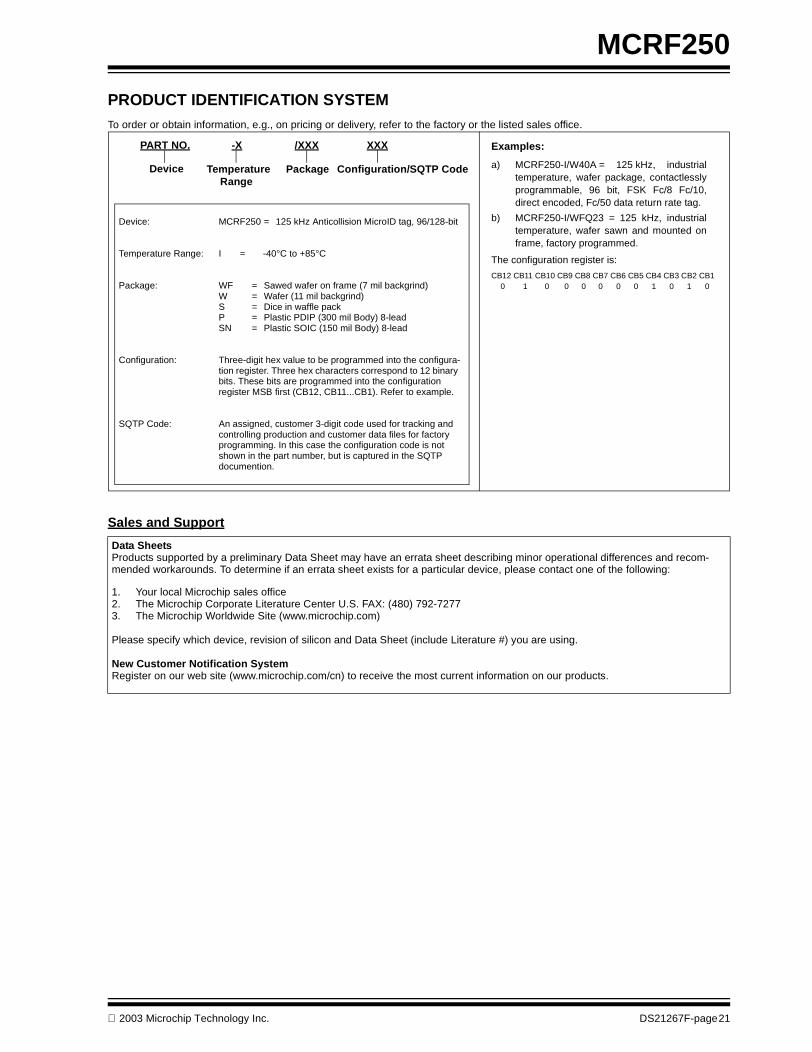
PRODUCT IDENTIFICATION SYSTEMTo order or obtain information, e.g., on pricing or delivery, refer to the factory or the listed sales office.
Sales and Support
Data SheetsProducts supported by a preliminary Data Sheet may have an errata sheet describing minor operational differences and recom-mended workarounds. To determine if an errata sheet exists for a particular device, please contact one of the following:
1. Your local Microchip sales office2. The Microchip Corporate Literature Center U.S. FAX: (480) 792-72773. The Microchip Worldwide Site (www.microchip.com)
Please specify which device, revision of silicon and Data Sheet (include Literature #) you are using.
New Customer Notification SystemRegister on our web site (www.microchip.com/cn) to receive the most current information on our products.
PART NO. -X /XXX
PackageTemperatureRange
Device
Device: MCRF250 = 125 kHz Anticollision MicroID tag, 96/128-bit
Temperature Range: I = -40°C to +85°C
Package: WF = Sawed wafer on frame (7 mil backgrind)W = Wafer (11 mil backgrind)S = Dice in waffle packP = Plastic PDIP (300 mil Body) 8-leadSN = Plastic SOIC (150 mil Body) 8-lead
Configuration: Three-digit hex value to be programmed into the configura-tion register. Three hex characters correspond to 12 binary bits. These bits are programmed into the configuration register MSB first (CB12, CB11...CB1). Refer to example.
SQTP Code: An assigned, customer 3-digit code used for tracking and controlling production and customer data files for factory programming. In this case the configuration code is not shown in the part number, but is captured in the SQTP documention.
Examples:
a) MCRF250-I/W40A = 125 kHz, industrialtemperature, wafer package, contactlesslyprogrammable, 96 bit, FSK Fc/8 Fc/10,direct encoded, Fc/50 data return rate tag.
b) MCRF250-I/WFQ23 = 125 kHz, industrialtemperature, wafer sawn and mounted onframe, factory programmed.
The configuration register is:
CB12 CB11 CB10 CB9 CB8 CB7 CB6 CB5 CB4 CB3 CB2 CB10 1 0 0 0 0 0 0 1 0 1 0
XXX
Configuration/SQTP Code
2003 Microchip Technology Inc. DS21267F-page21
MCRF250
NOTES:
DS21267F-page22 2003 Microchip Technology Inc.
Note the following details of the code protection feature on Microchip devices:
• Microchip products meet the specification contained in their particular Microchip Data Sheet.
• Microchip believes that its family of products is one of the most secure families of its kind on the market today, when used in the intended manner and under normal conditions.
• There are dishonest and possibly illegal methods used to breach the code protection feature. All of these methods, to our knowledge, require using the Microchip products in a manner outside the operating specifications contained in Microchip's Data Sheets. Most likely, the person doing so is engaged in theft of intellectual property.
• Microchip is willing to work with the customer who is concerned about the integrity of their code.
• Neither Microchip nor any other semiconductor manufacturer can guarantee the security of their code. Code protection does not mean that we are guaranteeing the product as “unbreakable.”
Code protection is constantly evolving. We at Microchip are committed to continuously improving the code protection features of ourproducts. Attempts to break microchip’s code protection feature may be a violation of the Digital Millennium Copyright Act. If such actsallow unauthorized access to your software or other copyrighted work, you may have a right to sue for relief under that Act.
Information contained in this publication regarding deviceapplications and the like is intended through suggestion onlyand may be superseded by updates. It is your responsibility toensure that your application meets with your specifications.No representation or warranty is given and no liability isassumed by Microchip Technology Incorporated with respectto the accuracy or use of such information, or infringement ofpatents or other intellectual property rights arising from suchuse or otherwise. Use of Microchip’s products as critical com-ponents in life support systems is not authorized except withexpress written approval by Microchip. No licenses are con-veyed, implicitly or otherwise, under any intellectual propertyrights.
2003 Microchip Technology Inc.
Trademarks
The Microchip name and logo, the Microchip logo, Accuron, dsPIC, KEELOQ, MPLAB, PIC, PICmicro, PICSTART, PRO MATE and PowerSmart are registered trademarks of Microchip Technology Incorporated in the U.S.A. and other countries.
AmpLab, FilterLab, microID, MXDEV, MXLAB, PICMASTER, SEEVAL, SmartShunt and The Embedded Control Solutions Company are registered trademarks of Microchip Technology Incorporated in the U.S.A.
Application Maestro, dsPICDEM, dsPICDEM.net, dsPICworks, ECAN, ECONOMONITOR, FanSense, FlexROM, fuzzyLAB, In-Circuit Serial Programming, ICSP, ICEPIC, microPort, Migratable Memory, MPASM, MPLIB, MPLINK, MPSIM, PICkit, PICDEM, PICDEM.net, PICtail, PowerCal, PowerInfo, PowerMate, PowerTool, rfLAB, rfPIC, Select Mode, SmartSensor, SmartTel and Total Endurance are trademarks of Microchip Technology Incorporated in the U.S.A. and other countries.
Serialized Quick Turn Programming (SQTP) is a service mark of Microchip Technology Incorporated in the U.S.A.
All other trademarks mentioned herein are property of their respective companies.
© 2003, Microchip Technology Incorporated, Printed in the U.S.A., All Rights Reserved.
Printed on recycled paper.
DS21267F-page 23
Microchip received ISO/TS-16949:2002 quality system certification for its worldwide headquarters, design and wafer fabrication facilities in Chandler and Tempe, Arizona and Mountain View, California in October 2003 . The Company’s quality system processes and procedures are for its PICmicro® 8-bit MCUs, KEELOQ® code hopping devices, Serial EEPROMs, microperipherals, non-volatile memory and analog products. In addition, Microchip’s quality system for the design and manufacture of development systems is ISO 9001:2000 certified.
DS21267F-page 24 2003 Microchip Technology Inc.
AMERICASCorporate Office2355 West Chandler Blvd.Chandler, AZ 85224-6199Tel: 480-792-7200 Fax: 480-792-7277Technical Support: 480-792-7627Web Address: http://www.microchip.com
Atlanta3780 Mansell Road, Suite 130Alpharetta, GA 30022Tel: 770-640-0034 Fax: 770-640-0307
Boston2 Lan Drive, Suite 120Westford, MA 01886Tel: 978-692-3848 Fax: 978-692-3821
Chicago333 Pierce Road, Suite 180Itasca, IL 60143Tel: 630-285-0071 Fax: 630-285-0075
Dallas4570 Westgrove Drive, Suite 160Addison, TX 75001Tel: 972-818-7423 Fax: 972-818-2924
DetroitTri-Atria Office Building 32255 Northwestern Highway, Suite 190Farmington Hills, MI 48334Tel: 248-538-2250Fax: 248-538-2260
Kokomo2767 S. Albright Road Kokomo, IN 46902Tel: 765-864-8360Fax: 765-864-8387
Los Angeles18201 Von Karman, Suite 1090Irvine, CA 92612Tel: 949-263-1888 Fax: 949-263-1338
Phoenix2355 West Chandler Blvd.Chandler, AZ 85224-6199Tel: 480-792-7966 Fax: 480-792-4338
San Jose1300 Terra Bella AvenueMountain View, CA 94043Tel: 650-215-1444
Toronto6285 Northam Drive, Suite 108Mississauga, Ontario L4V 1X5, CanadaTel: 905-673-0699 Fax: 905-673-6509
ASIA/PACIFICAustraliaSuite 22, 41 Rawson StreetEpping 2121, NSWAustraliaTel: 61-2-9868-6733 Fax: 61-2-9868-6755China - BeijingUnit 706BWan Tai Bei Hai Bldg.No. 6 Chaoyangmen Bei Str. Beijing, 100027, ChinaTel: 86-10-85282100 Fax: 86-10-85282104China - ChengduRm. 2401-2402, 24th Floor, Ming Xing Financial TowerNo. 88 TIDU StreetChengdu 610016, ChinaTel: 86-28-86766200 Fax: 86-28-86766599China - FuzhouUnit 28F, World Trade PlazaNo. 71 Wusi RoadFuzhou 350001, ChinaTel: 86-591-7503506 Fax: 86-591-7503521China - Hong Kong SARUnit 901-6, Tower 2, Metroplaza223 Hing Fong RoadKwai Fong, N.T., Hong KongTel: 852-2401-1200 Fax: 852-2401-3431China - ShanghaiRoom 701, Bldg. BFar East International PlazaNo. 317 Xian Xia RoadShanghai, 200051Tel: 86-21-6275-5700 Fax: 86-21-6275-5060China - ShenzhenRm. 1812, 18/F, Building A, United PlazaNo. 5022 Binhe Road, Futian DistrictShenzhen 518033, ChinaTel: 86-755-82901380 Fax: 86-755-8295-1393China - ShundeRoom 401, Hongjian BuildingNo. 2 Fengxiangnan Road, Ronggui TownShunde City, Guangdong 528303, ChinaTel: 86-765-8395507 Fax: 86-765-8395571China - QingdaoRm. B505A, Fullhope Plaza,No. 12 Hong Kong Central Rd.Qingdao 266071, ChinaTel: 86-532-5027355 Fax: 86-532-5027205IndiaDivyasree Chambers1 Floor, Wing A (A3/A4)No. 11, O’Shaugnessey RoadBangalore, 560 025, IndiaTel: 91-80-2290061 Fax: 91-80-2290062JapanBenex S-1 6F3-18-20, ShinyokohamaKohoku-Ku, Yokohama-shiKanagawa, 222-0033, JapanTel: 81-45-471- 6166 Fax: 81-45-471-6122
Korea168-1, Youngbo Bldg. 3 FloorSamsung-Dong, Kangnam-KuSeoul, Korea 135-882Tel: 82-2-554-7200 Fax: 82-2-558-5932 or 82-2-558-5934Singapore200 Middle Road#07-02 Prime CentreSingapore, 188980Tel: 65-6334-8870 Fax: 65-6334-8850TaiwanKaohsiung Branch30F - 1 No. 8Min Chuan 2nd RoadKaohsiung 806, TaiwanTel: 886-7-536-4818Fax: 886-7-536-4803TaiwanTaiwan Branch11F-3, No. 207Tung Hua North RoadTaipei, 105, TaiwanTel: 886-2-2717-7175 Fax: 886-2-2545-0139
EUROPEAustriaDurisolstrasse 2A-4600 WelsAustriaTel: 43-7242-2244-399Fax: 43-7242-2244-393DenmarkRegus Business CentreLautrup hoj 1-3Ballerup DK-2750 DenmarkTel: 45-4420-9895 Fax: 45-4420-9910FranceParc d’Activite du Moulin de Massy43 Rue du Saule TrapuBatiment A - ler Etage91300 Massy, FranceTel: 33-1-69-53-63-20 Fax: 33-1-69-30-90-79GermanySteinheilstrasse 10D-85737 Ismaning, GermanyTel: 49-89-627-144-0 Fax: 49-89-627-144-44ItalyVia Quasimodo, 1220025 Legnano (MI)Milan, Italy Tel: 39-0331-742611 Fax: 39-0331-466781NetherlandsP. A. De Biesbosch 14NL-5152 SC Drunen, NetherlandsTel: 31-416-690399 Fax: 31-416-690340United Kingdom505 Eskdale RoadWinnersh TriangleWokingham Berkshire, England RG41 5TUTel: 44-118-921-5869Fax: 44-118-921-5820
11/24/03
WORLDWIDE SALES AND SERVICE