microID® 125 kHz RFID System Design Guide
210
2004 Microchip Technology Inc. DS51115F microID ® 125 kHz RFID System Design Guide
Transcript of microID® 125 kHz RFID System Design Guide

2004 Microchip Technology Inc. DS51115F
microID® 125 kHz RFIDSystem Design Guide

DATA SHEET MARKINGS
Microchip uses various data sheet markings to designate each document phase as it relates to the product develop-ment stage. The markings appear at the bottom of the data sheet, between the copyright and document and pagenumbers. The definitions for each marking are provided below for your use.
Marking Description
Advance Information The information is on products in the design phase. Your designs should not be finalized with this information as revised information will be published when the product becomes available.
Preliminary This is preliminary information on new products in production but not yet fully characterized. The specifications in these data sheets are subject to change without notice. Before you finalize your design, please ensure that you have the most current revision of the data sheet by contacting your Microchip sales office.
No Marking Information contained in the data sheet is on products in full production.
Information contained in this publication regarding deviceapplications and the like is provided only for your convenienceand may be superseded by updates. It is your responsibility toensure that your application meets with your specifications.MICROCHIP MAKES NO REPRESENTATIONS OR WAR-RANTIES OF ANY KIND WHETHER EXPRESS OR IMPLIED,WRITTEN OR ORAL, STATUTORY OR OTHERWISE,RELATED TO THE INFORMATION, INCLUDING BUT NOTLIMITED TO ITS CONDITION, QUALITY, PERFORMANCE,MERCHANTABILITY OR FITNESS FOR PURPOSE.Microchip disclaims all liability arising from this information andits use. Use of Microchip’s products as critical components inlife support systems is not authorized except with expresswritten approval by Microchip. No licenses are conveyed,implicitly or otherwise, under any Microchip intellectual propertyrights.
DS51115F-page ii
Trademarks
The Microchip name and logo, the Microchip logo, Accuron, dsPIC, KEELOQ, microID, MPLAB, PIC, PICmicro, PICSTART, PRO MATE, PowerSmart, rfPIC, and SmartShunt are registered trademarks of Microchip Technology Incorporated in the U.S.A. and other countries.
AmpLab, FilterLab, Migratable Memory, MXDEV, MXLAB, PICMASTER, SEEVAL, SmartSensor and The Embedded Control Solutions Company are registered trademarks of Microchip Technology Incorporated in the U.S.A.
Analog-for-the-Digital Age, Application Maestro, dsPICDEM, dsPICDEM.net, dsPICworks, ECAN, ECONOMONITOR, FanSense, FlexROM, fuzzyLAB, In-Circuit Serial Programming, ICSP, ICEPIC, MPASM, MPLIB, MPLINK, MPSIM, PICkit, PICDEM, PICDEM.net, PICLAB, PICtail, PowerCal, PowerInfo, PowerMate, PowerTool, rfLAB, rfPICDEM, Select Mode, Smart Serial, SmartTel and Total Endurance are trademarks of Microchip Technology Incorporated in the U.S.A. and other countries.
SQTP is a service mark of Microchip Technology Incorporated in the U.S.A.
All other trademarks mentioned herein are property of their respective companies.
© 2004, Microchip Technology Incorporated, Printed in the U.S.A., All Rights Reserved.
Printed on recycled paper.
2004 Microchip Technology Inc.
Microchip received ISO/TS-16949:2002 quality system certification for its worldwide headquarters, design and wafer fabrication facilities in Chandler and Tempe, Arizona and Mountain View, California in October 2003. The Company’s quality system processes and procedures are for its PICmicro® 8-bit MCUs, KEELOQ® code hopping devices, Serial EEPROMs, microperipherals, nonvolatile memory and analog products. In addition, Microchip’s quality system for the design and manufacture of development systems is ISO 9001:2000 certified.

M
PAGE
Table of Contents
AN680 PASSIVE RFID BASICS
Introduction........................................................................................................................................ 1Definitions.......................................................................................................................................... 2System Handshake ........................................................................................................................... 4Backscatter Modulation..................................................................................................................... 4Data Encoding................................................................................................................................... 4Data Modulation for 125 kHz devices (MCRF2XX) ........................................................................... 6Anti-Collision ..................................................................................................................................... 7
MCRF200 DATA SHEET
Features ............................................................................................................................................. 9Application.......................................................................................................................................... 91.0 Electrical Characteristics .......................................................................................................... 112.0 Function Description................................................................................................................. 12
2.1 RF Front-End..................................................................................................................... 122.2 Configuration Register and Control Logic ......................................................................... 132.3 Memory Section ................................................................................................................ 142.4 Examples of Configuration Settings .................................................................................. 14
3.0 Modes Of Operation ................................................................................................................. 163.1 Native Mode ...................................................................................................................... 163.2 Read Mode........................................................................................................................ 16
4.0 Contactless Programming ........................................................................................................ 175.0 Mechanical Specifications For Die And Wafer ......................................................................... 196.0 Failed Die Identification ............................................................................................................ 217.0 Wafer Delivery Documentation................................................................................................. 218.0 Notice On Die And Wafer Handling.......................................................................................... 219.0 Packaging Information.............................................................................................................. 22
9.1 Package Marking Information............................................................................................ 22
MCRF250 DATA SHEET
1.0 Electrical Characteristics .......................................................................................................... 292.0 Functional Description.............................................................................................................. 30
2.1 RF Front-End..................................................................................................................... 302.2 Configuration Register and Control Logic ......................................................................... 312.3 Memory Section ................................................................................................................ 322.4 Examples of Configuration Settings .................................................................................. 32
3.0 Modes of Operation.................................................................................................................. 343.1 Native Mode ...................................................................................................................... 343.2 Read Mode........................................................................................................................ 34
4.0 Contactless Programming ........................................................................................................ 355.0 Anti-Collision ............................................................................................................................ 376.0 Mechanical Specifications for Die and Wafer........................................................................... 387.0 Failed Die Identification ............................................................................................................ 408.0 Wafer Delivery Documentation................................................................................................. 409.0 Notice on Die and Wafer Handling ........................................................................................... 4010.0 Packaging Information............................................................................................................ 41
10.1 Package Marking Information.......................................................................................... 41
2004 Microchip Technology Inc. DS51115F-page iii

M
PAGE
Table of Contents (Continued)
TB023 CONTACT PROGRAMMING SUPPORT
Introduction...................................................................................................................................... 47Definitions......................................................................................................................................... 47File Specifications ............................................................................................................................ 47
AN710 ANTENNA CIRCUIT DESIGN FOR RFID APPLICATION
Introduction....................................................................................................................................... 49Review of a Basic Theory for RFID Antenna Design ....................................................................... 49Induced Voltage in an Antenna Coil ................................................................................................ 51Wire Types and Ohmic Losses ....................................................................................................... 54Inductance of Various Antenna Coils .............................................................................................. 57Configuration of Antenna Circuits.................................................................................................... 67Consideration on Quality Factor Q and Bandwidth of Tuning Circuit .............................................. 69Resonant Circuits ............................................................................................................................ 70Tuning Method ................................................................................................................................ 73Read Range of RFID Devices......................................................................................................... 74References ...................................................................................................................................... 95
FSK READER REFERENCE DESIGN
Introduction...................................................................................................................................... 97Reader Circuits................................................................................................................................ 971.0 Transmitting Section................................................................................................................. 982.0 Receiving Section..................................................................................................................... 983.0 microID FSK Reader ................................................................................................................ 994.0 FSK Reader Schematic.......................................................................................................... 1015.0 FSK Reader Bill of Materials .................................................................................................. 1026.0 FSK Source Code for the PICmicro® MCU ............................................................................ 104
PSK READER REFERENCE DESIGN
1.0 Introduction.............................................................................................................................. 1132.0 Reader Circuits........................................................................................................................ 113
2.1 Transmitting Section........................................................................................................ 1142.2 Receiving Section............................................................................................................ 114
3.0 microID PSK Reader............................................................................................................... 1154.0 PSK Reader Schematic.......................................................................................................... 1175.0 PSK Reader Bill of Materials .................................................................................................. 1186.0 PSK Source Code for the PICmicro® MCU............................................................................ 121
ASK READER REFERENCE DESIGN
1.0 Introduction............................................................................................................................. 1312.0 Reader Circuits....................................................................................................................... 131
2.1 Transmitting Section........................................................................................................ 1322.2 Receiving Section............................................................................................................ 132
3.0 microID ASK Reader.............................................................................................................. 1334.0 ASK Reader Schematic.......................................................................................................... 1345.0 ASK Reader Bill of Materials .................................................................................................. 1356.0 ASK Reader Source Code for the PICmicro® MCU ............................................................... 137
DS51115F-page iv 2004 Microchip Technology Inc.

M
PAGE
Table of Contents
FSK ANTI-COLLISION READER REFERENCE DESIGN
1.0 Introduction............................................................................................................................. 1532.0 Reader Circuits....................................................................................................................... 1543.0 Anti-Collision Reader Schematic............................................................................................ 1564.0 Anti-collision Reader Bill of Materials ..................................................................................... 1575.0 FSK Anti-Collision Source Code for the PICmicro® MCU ....................................................... 159
USING THE microID® PROGRAMMER
1.0 Introduction.............................................................................................................................. 1712.0 Programming Signal Waveform ............................................................................................. 172
2.1 Power-up, Gap and Verification Signals.......................................................................... 1722.2 Programming Sequence.................................................................................................. 172
3.0 Calibration of Programming Voltage ...................................................................................... 1744.0 Programming Procedure ........................................................................................................ 176
4.1 Error Conditions .............................................................................................................. 1764.2 Programming Precautions............................................................................................... 176
5.0 Programming in a Standard Terminal Mode .......................................................................... 1785.1 Programmer Wake-up ..................................................................................................... 1785.2 Blank Check .................................................................................................................... 1785.3 Program and Verify the Device ....................................................................................... 1785.4 Error Conditions .............................................................................................................. 178
6.0 microID® Programmer Schematic ......................................................................................... 1817.0 microID® Programmer Bill of Materials .................................................................................. 1828.0 Programmer Source Code for PIC16C73............................................................................... 184
WORLDWIDE SALES AND SERVICE
2004 Microchip Technology Inc. DS51115F-page v

MTable of Contents
DS51115F-page vi © 2004 Microchip Technology Inc.

AN680Passive RFID Basics
INTRODUCTION
Radio Frequency Identification (RFID) systems useradio frequency to identify, locate and track people,assets and animals. Passive RFID systems arecomposed of three components – a reader (interroga-tor), passive tag and host computer. The tag is com-posed of an antenna coil and a silicon chip thatincludes basic modulation circuitry and non-volatilememory. The tag is energized by a time-varyingelectromagnetic radio frequency (RF) wave that istransmitted by the reader. This RF signal is called acarrier signal. When the RF field passes through anantenna coil, there is an AC voltage generated acrossthe coil. This voltage is rectified to result in a DC volt-age for the device operation. The device becomesfunctional when the DC voltage reaches a certain level.The information stored in the device is transmitted backto the reader. This is often called backscattering. Bydetecting the backscattering signal, the informationstored in the device can be fully identified.
There are two classes of RFID device depending ontype of memory cell : (a) read only device and (b) readand write device. The memory cell can be made ofEEPROM or FRAM. EEPROM is based on CMOS sili-con and FRAM is based on ferroelectric memory.Since CMOS process technology has been matured,the EEPROM can be produced relatively at lower costthan the FRAM device. However, FRAM based RFIDdevice consumes less power which is desirable for lowpower device. Therefore, it is known as a good candi-date for the future RFID device, if its manufacturingcost becomes compatible to that of the CMOS technol-ogy.
Because of its simplicity for use, the passive RFIDsystem has been used for many years in various RFremote sensing applications. Specifically in accesscontrol and animal tracking applications.
In recent years, there have been dramatic increases inapplication demands. In most cases, each applicationsuses a unique packaging form factor, communicationprotocol, frequency, etc. Because the passive tag isremotely powered by reader’s RF signal, it deals withvery small power (~ µw). Thus, the read range (com-munication distance between reader and tag) is typi-cally limited within a proximity distance. The read rangevaries with design parameters such as frequency, RFpower level, reader’s receiving sensitivity, size ofantenna, data rate, communication protocol, currentconsumptions of the silicon device, etc.
Low frequency bands (125 kHz-400 kHz) were tradi-tionally used in RFID applications. This was because ofthe availability of silicon devices. Typical carrierfrequency (reader’s transmitting frequency) in today’sapplications range from 125 kHz-2.4 GHz.
In recent years, the applications with high frequency(4-20 MHz) and microwave (2.45 GHz) bands haverisen with the advent of new silicon devices. Each fre-quency band has advantages and disadvantages. The4-20 MHz frequency bands offer the advantages of low(125 kHz) frequency and microwave (2.4 GHz) bands.Therefore, this frequency band becomes the mostdominant frequency band in passive RFID applications.
FIGURE 1: SIMPLE CONFIGURATION OF RFID SYSTEMS
Author: Youbok Lee and Pete SorrellsMicrochip Technology Inc.
Reader(Interrogator)
RF
SignalEnergizing/Command
BackscatteringData Signal
PassiveRFIDTag
HostComputer
RS-232
2001 Microchip Technology Inc. DS00680C-page 1

microID® 125 kHz Design Guide
DEFINITIONS
READER, INTERROGATOR
RFID reader is used to activate passive tag with RFenergy and to extract information from the tag.
For this function, the reader includes RF transmission,receiving and data decoding sections. In addition, thereader includes a serial communication (RS-232) capa-bility to communicate with the host computer. Depend-ing on the complexity and purpose of applications, thereader’s price range can vary from ten dollars to a fewthousand dollar worth of components and packaging.
The RF transmission section includes an RF carriergenerator, antenna and a tuning circuit. The antennaand its tuning circuit must be properly designed andtuned for the best performance. See Application NoteAN710 (DS00710) for the antenna circuit design.
Data decoding for the received signal is accomplishedusing a microcontroller. The firmware algorithm in themicrocontroller is written in such a way to transmit theRF signal, decode the incoming data and communi-cate with the host computer.
Typicall, reader is a read only device, while the readerfor read and write device is often called interrogator.Unlike the reader for read only device, the interrogatoruses command pulses to communicate with tag forreading and writing data.
TAG
Tag consists of a silicon device and antenna circuit.
The purpose of the antenna circuit is to induce an ener-gizing signal and to send a modulated RF signal. Theread range of tag largely depends upon the antennacircuit and size.
The antenna circuit of tag is made of LC resonantcircuit or E-field dipole antenna, depending on thecarrier frequency. The LC resonant circuit is used forthe frequency of less than 100 MHz. In this frequencyband, the communication between the reader and tagtakes place with magnetic coupling between the twoantennas through the magnetic field. The antennautilizing the inductive coupling is often called magneticdipole antenna.
The antenna circuit must be designed such a way tomaximize the magnetic coupling between them. Thiscan be achieved with the following parameters:
a) LC circuit must be tuned to the carrier frequencyof the reader
b) Maximize Q of the tuned circuit
c) Maximize antenna size within physical limit ofapplication requirement.
See Application Note AN710 for more details.
When the frequency goes above 100 MHz, the require-ment of LC values for its resonant frequency becomestoo small to realize with discrete L and C components.As frequency increases, the wavelength is gettingshorter. In this case, a true E-field antenna can bemade of a simple conductor that has linear dimensionless than or equivalent to half (½) the wavelength of thesignal. The antenna that is made of a simple conductoris called electric dipole antenna. The electric dipoleantenna utilizes surface current that is generated by anelectric field (E-Field). The surface current on theconductor produces voltage at load. This voltage isused to energize the silicon device. Relatively simpleantenna structure is formed for the higher frequencycompared to the lower frequency.
READ-ONLY DEVICE, READ/WRITE DEVICE:
For the read only device, the information that is in thememory can’t be changed by RF command once it hasbeen written.
Read only devices are programmed as follows: (a) inthe factory as a part of manufacturing process, (b) con-tactlessly programmed one time after the manufactur-ing (MCRF200 and MCRF250) or (c) can beprogrammed and also reprogrammed in contact mode(MCRF355 and MCRF360).
A device with memory cells that can be reprogrammedby RF commands is called read/write device. Theinformation in the memory can be reprogrammed byInterrogator command.
Memory in today’s RFID device is made of (a) CMOSor (b) FRAM array. The CMOS memory cell needshigher voltage for writing than reading. In the passiveread/write device, the programming voltage is gener-ated by multiplying the rectified voltage. The voltagemultiplier circuit is often called a charge pumper. Inaddition to the programming voltage, the read/writedevice needs command decoder and other controllerlogics. As a result, the read/write device needs morecircuit building blocks than that of the read only device.Therefore, the device size is larger and cost more thana read only device. The FRAM device needs the samevoltage for reading and writing. However, its manufac-turing cost is much higher than CMOS technology.Most of RFID device available today’s market place areCMOS based device.
DS00680C-page 2 2001 Microchip Technology Inc.

AN680
READ/WRITE RANGE
Read/write range is a communication distancebetween the reader (Interrogator) and tag. Specifically,the read range is a maximum distance to read data outfrom the tag and write range is a maximum distance towrite data from interrogator to tag.
The read/write range is related to:
(1) Electromagnetic coupling of the reader (interroga-tor) and tag antennas, (2) RF Output power level ofreader (interrogator), (3) Carrier frequency bands, (4)Power consumption of device, etc.
The electromagnetic coupling of reader and tag anten-nas increases using similar size of antenna with higherQ in both sides. The read range is improved by increas-ing the carrier frequency. This is due to the gain in theradiation efficiency of the antenna as the frequencyincreases. However, the disadvantage of highfrequency (900 MHz-2.4 GHz) application are shallowskin depth and narrower antenna beam width. Thesecause less penetration and more directional problem,respectively. Low frequency application, on the otherhand, has advantage in the penetration and directional,but a disadvantage in the antenna performance.
The read range increases by reducing the currentconsumptions in the silicon device. This is becauseadditional radiating power is available by reducing thepower dissipation in the silicon device.
MODULATION PROTOCOL
The passive RFID tag uses backscattering of thecarrier frequency for sending data from the tag toreader. The amplitude of backscattering signal is mod-ulated with modulation data of the tag device. Themodulation data can be encoded in the form of ASK(NRZ or Manchester), FSK or PSK. Therefore, themodulation signal from the tag is Amplitude-Amplitude,Amplitude-FSK and Amplitude-PSK. See MicroID 125kHz Design Guide for Amplitude, Amplitude-FSK andAmplitude-PSK reader.
CARRIER
Carrier is the transmitting radio frequency of reader(interrogator). This RF carrier provides energy to thetag device, and is used to detect modulation data fromthe tag using backscattering. In read/write device, thecarrier is also used to deliver interrogator’s commandand data to the tag.
Typical passive RFID carrier frequencies are:
a) 125 kHz-400 kHzb) 4 MHz-24 MHzc) 900 MHz-2.45 GHz.
The frequency bands must be selected carefully forapplications because each one has its own advantagesand disadvantages. Table 1 shows the characteristic ofeach frequency bands.
TABLE 1:
Frequency BandsAntenna
Components
Read Range
(typical)
Penertration (skin depth)
Orientation(Directionality)
Usability in metal or humid
environment
Applications(typical)
Low Frequency(125 - 400) kHz
Coil (> 100 turns) and capacitor
Proximity (8”)
Best Least Possible Proximity
Medium Frequency(4 MHz - 24 MHz)
Coil (< 10 turns) and capacitor
Medium (15”)
Good Not much Possible Low cost and high volume
High Frequency(>900 MHz)
E-field dipole(a piece of conductor)
Long ( > 1 m)
Poor Very high Difficult Line of sight with long
range
2001 Microchip Technology Inc. DS00680C-page 3

microID® 125 kHz Design Guide
SYSTEM HANDSHAKE
Typical handshake of a tag and reader (interrogator) isas follows:
A. Read Only Tag
1. The reader continuously transmits an RF signaland watches always for modulated backscatter-ing signal.
2. Once the tag has received sufficient energy tooperate correctly, it begins clocking its data to amodulation transistor, which is connectedacross the antenna circuit.
3. The tag’s modulation transistor shorts theantenna circuit, sequentially corresponding tothe data which is being clocked out of the mem-ory array.
4. Shorting and releasing the antenna circuitaccordingly to the modulation data causesamplitude fluctuation of antenna voltage acrossthe antenna circuit.
5. The reader detects the amplitude variation of thetag and uses a peak-detector to extract the mod-ulation data.
B. Read and Write Tag
(Example: MCRF45X devices with FRR and ReaderTalks First mode)
1. The interrogator sends a command to initiatecommunication with tags in the fields. This com-mand signal is also used for energizing the pas-sive device.
2. Once the tag has received sufficient energy andcommand, it responses back with its ID foracknowledgment.
3. The interrogator now knows which tag is in thefield. The interrogator sends a command to theidentified tag for what to do next: processing(read or write) or sleep.
4. If the tag receive processing and reading com-mands, it transmits a specified block data andwaits for the next command.
5. If the tag receives processing and writing com-mands along with block data, it writes the blockdata into the specified memory block, and trans-mits the written block data for verification.
6. After the processing, the interrogator sends an“end” command to send the tag into the sleep(“silent”) mode.
7. If the device receives “end” command after pro-cessing, it sends an acknowledgement (8-bitpreamble) and stays in sleep mode. During thesleep mode, the device remains in non-modulat-ing (detuned) condition as long as it remains inthe power-up. This time the handshake is over.
8. The interrogator is now looking for the next tagfor processing, establishes an handshake andrepeats the processing.
9. See Fig.4-1 in MCRF45x Data sheet for moredetails.
BACKSCATTER MODULATION
This terminology refers to the communication methodused by a passive RFID tag to send data to the readerusing the same reader’s carrier signal. The incomingRF carrier signal to the tag is transmitted back to thereader with tag’s data.
The RF voltage induced in the tag’s antenna is ampli-tude-modulated by the modulation signal (data) of tagdevice. This amplitude-modulation can be achieved byusing a modulation transistor across the LC resonantcircuit or partially across the resonant circuit.
The changes in the voltage amplitude of tag’s antennacan affect on the voltage of the reader antenna. Bymonitoring the changes in the reader antenna voltage(due to the tag’s modulation data), the data in the tagcan be reconstructed.
The RF voltage link between reader and tag antennasare often compared to a weakly coupled transformercoils; as the secondary winding (tag coil) is momen-tarily shunted, the primary winding (reader coil) experi-ences a momentary voltage drop.
DATA ENCODING
Data encoding refers to processing or altering the databitstream in-between the time it is retrieved from theRFID chip’s data array and its transmission back to thereader. The various encoding algorithms affect errorrecovery, cost of implementation, bandwidth, synchro-nization capability and other aspects of the systemdesign. Entire textbooks are written on the subject, butthere are several popular methods used in RFIDtagging today:
1. NRZ (Non-Return to Zero) Direct. In thismethod no data encoding is done at all; the 1’sand 0’s are clocked from the data array directlyto the output transistor. A low in thepeak-detected modulation is a ‘0’ and a high isa ‘1’.
2. Differential Biphase. Several different forms ofdifferential biphase are used, but in general thebitstream being clocked out of the data array ismodified so that a transition always occurs onevery clock edge, and 1’s and 0’s are distin-guished by the transitions within the middle ofthe clock period. This method is used to embedclocking information to help synchronize thereader to the bitstream. Because it always has atransition at a clock edge, it inherently providessome error correction capability. Any clock edgethat does not contain a transition in the datastream is in error and can be used to reconstructthe data.
DS00680C-page 4 2001 Microchip Technology Inc.

AN680
3. Biphase_L (Manchester). This is a variation ofbiphase encoding in which there is not always atransition at the clock edge. The MCRF355/360and MCRF45X devices use this encodingmethod.
FIGURE 2: VARIOUS DATA CODING WAVEFORMS
Data
NRZ_L
Biphase_L(Manchester)
DifferentialBiphase_S
SIGNAL WAVEFORM DESCRIPTION
Digital Data
Non-Return to Zero – Level
‘1’ is represented by logic high level.‘0’ is represented by logic low level.
Biphase – Level (Split Phase)A level change occurs at middle of every bit clock period.
‘1’ is represented by a high to low level change at midclock.‘0’ is represented by a low to high
level change at midclock.
Differential Biphase – Space
‘1’ is represented by a change in level at start of clock.‘0’ is represented by no change in
Bit Rate Clock Signal
(Direct)
CLK
A level change occurs at middle ofevery bit clock period.
level at start of clock.
1 0 1 1 0 0 0 1 1 0 1 0
Note: Manchester coding is used for the MCRF355/360 and MCRF45X
2001 Microchip Technology Inc. DS00680C-page 5

microID® 125 kHz Design Guide
DATA MODULATION FOR 125 kHz DEVICES (MCRF2XX)
Although all the data is transferred to the host byamplitude-modulating the carrier (backscatter modula-tion), the actual modulation of 1’s and 0’s is accom-plished with three additional modulation methods:
1. Direct. In direct modulation, the AmplitudeModulation of the backscatter approach is theonly modulation used. A high in the envelope isa ‘1’ and a low is a ‘0’. Direct modulation canprovide a high data rate but low noise immunity.
2. FSK (Frequency Shift Keying). This form ofmodulation uses two different frequencies fordata transfer; the most common FSK mode isFC/8/10. In other words, a ‘0’ is transmitted asan amplitude-modulated clock cycle with periodcorresponding to the carrier frequency dividedby 8, and a ‘1’ is transmitted as anamplitude-modulated clock cycle period corre-sponding to the carrier frequency divided by 10.The amplitude modulation of the carrier thusswitches from FC/8 to FC/10 corresponding to
0’s and 1’s in the bitstream, and the reader hasonly to count cycles between the peak-detectedclock edges to decode the data. FSK allows fora simple reader design, provides very strongnoise immunity, but suffers from a lower datarate than some other forms of data modulation.In Figure 3, FSK data modulation is used withNRZ encoding.
3. PSK (Phase Shift Keying). This method of datamodulation is similar to FSK, except only onefrequency is used, and the shift between 1’s and0’s is accomplished by shifting the phase of thebackscatter clock by 180 degrees. Two commontypes of PSK are:
• Change phase at any ‘0’, or • Change phase at any data change
(0 to 1 or 1 to 0).
PSK provides fairly good noise immunity, amoderately simple reader design, and a fasterdata rate than FSK. Typical applications utilize abackscatter clock of FC/2, as shown in Figure 4.
FIGURE 3: FSK MODULATED SIGNAL, FC/8 = 0, FC/10 = 1
8 cycles = 0 8 cycles = 0 10 cycles = 1 10 cycles = 1 8 cycles = 0
DS00680C-page 6 2001 Microchip Technology Inc.

AN680
FIGURE 4: PSK MODULATED SIGNAL
ANTI-COLLISION
In many existing applications, a single-read RFID tag issufficient and even necessary: animal tagging andaccess control are examples. However, in a growingnumber of new applications, the simultaneous readingof several tags in the same RF field is absolutely criti-cal: library books, airline baggage, garment and retailapplications are a few.
In order to read multiple tags simultaneously, the tagand reader must be designed to detect the conditionthat more than one tag is active. Otherwise, the tagswill all backscatter the carrier at the same time and theamplitude-modulated waveforms shown in Figure 3and Figure 4 would be garbled. This is referred to as acollision. No data would be transferred to the reader.The tag/reader interface is similar to a serial bus, eventhough the “bus” travels through the air. In a wiredserial bus application, arbitration is necessary to pre-vent bus contention. The RFID interface also requiresarbitration so that only one tag transmits data over the“bus” at one time.
A number of different methods are in use and indevelopment today for preventing collisions; most arepatented or patent pending. Yet, all are related tomaking sure that only one tag “talks” (backscatters) atany one time. See the MCRF250 (DS21267),MCRF355/360 (DS21287) and MCRF45X (DS40232)data sheets for various anti-collision algorithms.
PhaseShift
PhaseShift
PhaseShift
PhaseShift
2001 Microchip Technology Inc. DS00680C-page 7

microID® 125 kHz Design Guide
NOTES:
DS00680C-page 8 2001 Microchip Technology Inc.

MCRF200125 kHz microID® Passive RFID Device
Features:
• Factory programming and memory serialization (SQTPSM)
• One-time contactless programmable (developer kit only)
• Read-only data transmission after programming
• 96 or 128 bits of One-Time Programmable (OTP) user memory (also supports 48 and 64-bit protocols)
• Typical operation frequency: 100 kHz-400 kHz
• Ultra low-power operation (5 µA @ VCC = 2V)• Modulation options:
- ASK, FSK, PSK
• Data Encoding options: - NRZ Direct, Differential Biphase, Manchester
Biphase• Die, wafer, COB, PDIP or SOIC package options• Factory programming options
Application:
• Low-cost alternative for existing low-frequency RFID devices
• Access control and time attendance
• Security systems• Animal tagging• Product identification
• Industrial tagging• Inventory control
Package Type
Description:
The microID® 125 kHz Design Guide is a passive RadioFrequency Identification (RFID) device for low-fre-quency applications (100 kHz-400 kHz). The device ispowered by rectifying an incoming RF signal from thereader. The device requires an external LC resonantcircuit to receive the incoming RF signal and to senddata. The device develops a sufficient DC voltage foroperation when its external coil voltage reachesapproximately 10 VPP.
This device has a total of 128 bits of user programmablememory and an additional 12 bits in its configurationregister. The user can manually program the 128 bits ofuser memory by using a contactless programmer in amicroID developer kit such as DV103001 or PG103001.However, in production volume the MCRF200 isprogrammed at the factory (Microchip SQTP – seeTechnical Bulletin TB023). The device is a One-TimeProgrammable (OTP) integrated circuit and operates asa read-only device after programming.
MCRF200Reader
RFSignal
Data
PDIP/SOICVA VB1
2
3
4
8
7
6
5
NC
I/O
RESET
NC
VSS
VCC
Note: Pins 3, 4, 5 and 6 are for device test purposes only.Pins 1 and 8 are for antenna connections.DO NOT ground pin 5.
2003 Microchip Technology Inc. DS21219H-page 9

microID® 125 kHz Design Guide
Block Diagram
The configuration register includes options for commu-nication protocol (ASK, FSK, PSK), data encodingmethod, data rate, and data length.These options arespecified by customer and factory programmed duringassembly. Because of its many choices of configurationoptions, the device can be easily used as an alternativeor second source for most of the existing low frequencypassive RFID devices available today.
The device has a modulation transistor between thetwo antenna connections (VA and VB). The modulationtransistor damps or undamps the coil voltage when itsends data. The variation of coil voltage controlled bythe modulation transistor results in a perturbation ofvoltage in reader antenna coil. By monitoring thechanges in reader coil voltage, the data transmittedfrom the device can be reconstructed.
The device is available in die, wafer, Chip-on-Board(COB) modules, PDIP, or SOIC packages. Factoryprogramming and memory serialization (SQTP) arealso available upon request. See TB023 for moreinformation on contact programming support.
The DV103001 developer’s kit includes ContactlessProgrammer, ASK, FSK, PSK reference readers, andreference design guide. The reference design guideincludes schematics for readers and contactlessprogrammer as well as in-depth document for antennacircuit designs.
Column
Memory Array
VCC
VSS
Rectifier
ClockGenerator
CoilConnections
Decode
RowDecode
Modulation Control
Counter
Data
Mod
ulat
ion
Circ
uit
DS21219H-page 10 2003 Microchip Technology Inc.

MCRF200
1.0 ELECTRICAL CHARACTERISTICS
Absolute Maximum Ratings (†)
Storage temperature .............................................................................................................................. - 65°C to +150°C
Ambient temperature with power applied................................................................................................-40°C to +125°C
Maximum current into coil pads ..............................................................................................................................50 mA
TABLE 1-1: AC AND DC CHARACTERISTICS
† NOTICE: Stresses above those listed under “Absolute Maximum Ratings” may cause permanent damage tothe device. This is a stress rating only and functional operation of the device at those or any other conditionsabove those indicated in the operational listings of this specification is not implied. Exposure to maximum ratingconditions for extended periods may affect device reliability.
All parameters apply across the specified operating ranges unless otherwise noted.
Industrial (I): TA = -40°C to +85°C
Parameter Sym Min Typ Max Units Conditions
Clock frequency FCLK 100 — 400 kHz
Contactless programming time TWC — 2 — sec For all 128-bit array
Data retention 200 — — Years at 25°C
Coil current (Dynamic) ICD — 50 µA
Operating current IDD — 5 µA VCC = 2V
Turn-on-voltage (Dynamic) for modulation
VAVB 10 — — VPP
VCC 2 — — VDC
Input Capacitance CIN — 2 — pF Between VA and VB
2003 Microchip Technology Inc. DS21219H-page 11

microID® 125 kHz Design Guide
2.0 FUNCTION DESCRIPTION
The device contains three major building blocks. Theyare RF front-end, configuration and control logic, andmemory sections. The Block Diagram is shown onpage 1.
2.1 RF Front-End
The RF front-end of the device includes circuits forrectification of the carrier, VDD (operating voltage) andhigh-voltage clamping. This section also includes aclock generator and modulation circuit.
2.1.1 RECTIFIER – AC CLAMP
The rectifier circuit rectifies RF voltage on the externalLC antenna circuit. Any excessive voltage on the tunedcircuit is clamped by the internal circuitry to a safe levelto prevent damage to the IC.
2.1.2 POWER-ON RESET
This circuit generates a Power-on Reset when the tagfirst enters the reader field. The Reset releases whensufficient power has developed on the VDD regulator toallow correct operation.
2.1.3 CLOCK GENERATOR
This circuit generates a clock based on the carrierfrequency from the reader. This clock is used to deriveall timing in the device, including the baud rate andmodulation rate.
2.1.4 MODULATION CIRCUIT
The device sends the encoded data to the reader byAM-modulating the coil voltage across the tuned LCcircuit. A modulation transistor is placed between thetwo antenna coil pads (VA and VB). The transistor turnson and off based on the modulation signal. As a result,the amplitude of the antenna coil voltage varies with themodulation signal. See Figure 2-1 for details.
FIGURE 2-1: MODULATION SIGNAL AND MODULATED SIGNAL
MCRF200
Modulation Signal
VA
VB
Modulation
Modulation Signal
Modulated RF Signal(across VA and VB)
L C
Amplitude
t
Transistor
DS21219H-page 12 2003 Microchip Technology Inc.

MCRF200
2.2 Configuration Register and Control Logic
The configuration register determines the operationalparameters of the device. The configuration registercan not be programmed contactlessly; it isprogrammed during wafer probe at the Microchipfactory. CB11 is always a zero; CB12 is set whensuccessful contact or contactless programming of thedata array has been completed. Once CB12 is set,device programming and erasing is disabled. Table 2-4contains a description of the bit functions of the controlregister.
2.2.1 BAUD RATE TIMING OPTION
The chip will access data at a baud rate determined bybits CB2, CB3 and CB4 of the configuration register.For example, MOD32 (CB2 = 0, CB3 = 1, CB4 = 1) has32 RF cycles per bit. This gives the data rate of 4 kHzfor the RF carrier frequency of 128 kHz.
The default timing is MOD128 (FCLK/128), and thismode is used for contact and contactless program-ming. Once the array is successfully programmed, thelock bit CB12 is set. When the lock bit is set, program-ming and erasing the device becomes permanentlydisabled. The configuration register has no effect ondevice timing until the EEPROM data array isprogrammed (CB12 = 1).
2.2.2 DATA ENCODING OPTION
This logic acts upon the serial data being read from theEEPROM. The logic encodes the data according to theconfiguration bits CB6 and CB7. CB6 and CB7determine the data encoding method. The availablechoices are:
• Non-return to zero-level (NRZ_L)• Biphase Differential, Biphase Manchester• Inverted Manchester
2.2.3 MODULATION OPTION
CB8 and CB9 determine the modulation protocol of theencoded data. The available choices are:
• ASK• FSK
• PSK_1• PSK_2
When ASK (direct) option is chosen, the encoded datais fed into the modulation transistor without change.
When FSK option is chosen, the encoded data isrepresented by:
a) Sets of 10 RF carrier cycles (first 5 cycles →higher amplitude, the last 5 cycles → loweramplitude) for logic “high” level.
b) Sets of 8 RF carrier cycles (first 4 cycles →higher amplitude, the last 4 cycles → loweramplitude) for logic “low” level.
For example, FSK signal for MOD40 is represented:
a) 4 sets of 10 RF carrier cycles for data ‘1’.
b) 5 sets of 8 RF carrier cycles for data ‘0’.
Refer to Figure 2-2 for the FSK signal with MOD40option.
The PSK_1 represents change in the phase of themodulation signal at the change of the encoded data.For example, the phase changes when the encodeddata is changed from ‘1’ to ‘0’, or from ‘0’ to ‘1’.
The PSK_2 represents change in the phase at thechange on ‘1’. For example, the phase changes whenthe encoded data is changed from ‘0’ to ‘1’, or from ‘1’to ‘1’.
FIGURE 2-2: ENCODED DATA AND FSK OUTPUT SIGNAL FOR MOD40 OPTION
Encoded Data ‘1’ Encoded Data ‘0’
40 RF cycles 40 RF cycles
5 cycles (HI)
5 cycles (LO)4 cycles (HI)
4 cycles (LO)
2003 Microchip Technology Inc. DS21219H-page 13

microID® 125 kHz Design Guide
FIGURE 2-3: PSK DATA MODULATION
2.2.4 MEMORY ARRAY LOCK BIT (CB12)
The CB12 must be ‘0’ for contactless programming(Blank). The bit (CB12) is automatically set to ‘1’ assoon as the device is programmed contactlessly.
2.3 Memory Section
The device has 128 bits of one-time programmable(OTP) memory. The user can choose 96 or 128 bits byselecting the CB1 bit in the configuration register. SeeTable 2-4 for more details.
2.3.1 COLUMN AND ROW DECODER LOGIC AND BIT COUNTER
The column and row decoders address the EEPROMarray at the clock rate and generate a serial datastream for modulation. This data stream can be up to128 bits in length. The size of the data stream is userprogrammable with CB1 and can be set to 96 or 128bits. Data lengths of 48 and 64 bits are available byprogramming the data twice in the array, end-to-end.
The column and row decoders route the proper voltageto the array for programming and reading. In theprogramming modes, each individual bit is addressedserially from bit 1 to bit 128.
2.4 Examples of Configuration Settings
EXAMPLE 2-1: “08D” CONFIGURATION
EXAMPLE 2-2: “00A” CONFIGURATION
EXAMPLE 2-3: MCRF200 CONFIGURATION FOR FDX-B ISO ANIMAL STANDARD PROTOCOL (ASP)
P
P
P P
PP
PP
PP
PP
‘0’ ‘0’ ‘1’‘1’Encoded Data
PSK_ 1Change on Data
PSK _2Change on ‘1’
(NRZ_L)
‘1’
The “08D” (hex) configuration is interpreted asfollows:
“08D” → 0000-1000-1101
Referring to Table 2-4, the “08D” configurationrepresents:
Modulation = PSK_1PSK rate = rf/2Data encoding = NRZ_L (direct)Baud rate = rf/32 = MOD32Memory size 128 bits
CB12 CB1
The “00A” (hex) configuration is interpreted asfollows:
“00A” → 0000-0000-1010
The MSB corresponds to CB12 and the LSBcorresponds to CB1 of the configuration register.Therefore, we have:
Referring to Table 2-4, the “00A” configurationrepresents:
Not programmed device (blank), anti-collision:disabled, FSK protocol, NRZ_L (direct) encod-ing, MOD50 (baud rate = rf/50), 96 bits.
CB12=0 CB11=0 CB10=0 CB9=0
CB8=0 CB7=0 CB6=0 CB5=0
CB4=1 CB3=0 CB2=1 CB1=0
CB12 CB1
The FDX-B ISO Specification is:
Modulation = ASKData encoding = Differential biphaseBaud rate = rf/32 = 4 Kbits/sec for 128 kHzMemory size = 128 bits
Referring to Table 2-4, the equivalent MCRF200configuration is: “14D”.
DS21219H-page 14 2003 Microchip Technology Inc.

MCRF200
TABLE 2-4: CONFIGURATION REGISTER
CB12 CB11 CB10 CB9 CB8 CB7 CB6 CB5 CB4 CB3 CB2 CB1
MEMORY SIZECB1 = 1 128-bit user memory arrayCB1 = 0 96-bit user memory array
BAUD RATE
SYNC WORDCB5 = 0 (Always)
DATA ENCODINGCB6 = 0; CB7 = 0 NRZ_L (Direct)CB6 = 0; CB7 = 1 Biphase_S (Differential)CB6 = 1; CB7 = 0 Biphase_L (Manchester)CB6 = 1; CB7 = 1 (Inverted Manchester)
MODULATION OPTIONSCB8 = 0; CB9 = 0 FSK 0 = Fc/8, 1 = Fc/10CB8 = 0; CB9 = 1 Direct (ASK)CB8 = 1; CB9 = 0 PSK_1(phase change on change of data)
CB8 = 1; CB9 = 1 PSK_2(phase change at beginning of a one)
PSK RATE OPTIONCB10 = 1 Carrier/4CB10 = 0 Carrier/2
(ANTI-COLLISION OPTION (Read-only)CB11 = 0 Disabled (Always)
MEMORY ARRAY LOCK BIT (Read-only)CB12 = 0 User memory array not locked (Blank)CB12 = 1 User memory array is locked
(Programmed)
CB2 CB3 CB4 Rate
0 0 0 MOD1280 0 1 MOD1000 1 0 MOD800 1 1 MOD321 0 0 MOD641 0 1 MOD501 1 0 MOD401 1 1 MOD16
2003 Microchip Technology Inc. DS21219H-page 15

microID® 125 kHz Design Guide
3.0 MODES OF OPERATION
The device has two basic modes of operation: Nativemode and Read mode.
3.1 Native Mode
Every unprogrammed blank device (CB12 = 0)operates in Native mode, regardless of configurationregister settings:
FCLK/128, FSK, NRZ_L (direct)
Once the user memory is programmed, the lock bit isset (CB12 = 1) which causes the MCRF200 to switchfrom Native mode to the Communication mode definedby the configuration register.
Refer to Figure 4-1 for contactless programmingsequence. Also see the microID® 125 kHz RFIDSystem Design Guide (DS51115) for more information.
3.2 Read Mode
After the device is programmed (CB12 = 1), the deviceis operated in the Read-only mode. The devicetransmits its data according to the protocol in theconfiguration register.
FIGURE 3-1: TYPICAL APPLICATION CIRCUIT
Pad VB
Pad VA
Input capacitance: 2 pFRF Signal
Data
C
To Readeramplifier/filter
From Reader
IAC
L
2.5 mH 648 pF
fres1
2π LC------------------- 125 kHz= =
125 kHz
MCRF200
L C
DS21219H-page 16 2003 Microchip Technology Inc.

MCRF200
4.0 CONTACTLESS PROGRAMMING
The contactless programming of the device is possiblefor blank devices (CB12 = 0) only and is recommendedfor only low-volume, manual operation during develop-ment. In volume production, the MCRF200 is normallyused as a factory programmed device only. Thecontactless programming timing sequence consists of:
a) RF power-up signal.b) Short gap (absence of RF field).c) Verify signal (continuous RF signal).
d) Programming signal.e) Device response with programmed data.
The blank device (CB12 = 0) understands the RFpower-up followed by a gap as a blank checkingcommand, and outputs 128 bits of FSK data with all ‘1’safter the short gap. To see this blank data (verify), thereader/programmer must provide a continuous RFsignal for 128 bit-time. (The blank (unprogrammed)device has all ‘F’s in its memory array. Therefore, theblank data should be all ‘1’s in FSK format). Since theblank device operates at Default mode (MOD128),there are 128 RF cycles for each bit. Therefore, thetime requirement to complete this verify is 128 bits x128 RF cycles/bit x 8 use/cycles = 131.1 msec for125 kHz signal.
As soon as the device completes the verify, it enters theprogramming mode. The reader/programmer mustprovide RF programming data right after the verify. Inthis programming mode, each bit lasts for 128 RFcycles. Refer to Figure 4-1 for the contactless program-ming sequence.
Customer must provide the following specific voltagefor the programming:
1. Power-up and verify signal = 13.5V ±1 VPP
2. Programming voltage:
- To program bit to ‘1’: 13.5V ±1 VPP
- To program bit to ‘0’: 30V ±2 VPP
After the programming cycle, the device outputsprogrammed data (response). The reader/programmercan send the programming data repeatedly after thedevice response until the programming is successfullycompleted. The device locks the CB12 as soon as theprogramming mode (out of field) is exited and becomesa read-only device.
Once the device is programmed (CB12 = 1), the deviceoutputs its data according to the configuration register.
The PG103001 (Contactless Programmer) is used forthe programming of the device. The voltage levelshown in Figure 4-1 is adjusted by R5 and R7 in thecontactless programmer. Refer to the MicroID®
125 kHz RFID System Design Guide (DS51115) formore information.
2003 Microchip Technology Inc. DS21219H-page 17

microID® 125 kHz Design Guide
FIGURE 4-1: CONTACTLESS PROGRAMMING SEQUENCE
Pow
er-u
pG
ap
~ 5
0 -
100
µs13
.5 ±
1 V
PP
Hig
h-P
ower
30 ±
2 V
PP
Bit
1B
it 2
128
bits
x 1
28 c
ycle
s/bi
t x 8
µs/c
ycle
= 1
31.1
ms
13.5
± 1
VP
P
Con
tact
less
Pro
gram
min
g P
roto
col
f = 1
25 k
Hz
t = 8
µs
Bit
3…
Pro
gra
m
1 bi
t = 1
28 c
ycle
s x
8µs
/cyc
le =
1.0
24m
s
80 -
180
µs
Ver
ify
FS
K S
ign
al
(R5)
128
bits
∆t =
Gua
rd B
and
0V
13.5
± 1
VP
P
(R5)
Low
-Pow
erS
igna
lS
igna
l
(R7)
No
te:
Low
-pow
er s
igna
l:le
aves
bit
= 1
Hig
h-po
wer
sig
nal:
prog
ram
s bi
t = 0
Def
ault
prog
ram
min
g pr
otoc
ol =
FS
K, F
c/8/
10, 1
28 b
itsF
or 9
6-bi
t pro
gram
min
g, b
its 3
3-64
are
“do
n’t c
are”
, but
all
128-
bit c
ycle
s m
ust b
e in
the
sequ
ence
.
DS21219H-page 18 2003 Microchip Technology Inc.

MCRF200
5.0 MECHANICAL SPECIFICATIONS FOR DIE AND WAFER
FIGURE 5-1: DIE PLOT
TABLE 5-1: PAD COORDINATES (µm)
TABLE 5-2: PAD FUNCTION TABLE
VB VA
VSS VCC RESET I/O
Device Test Only
Passivation Openings
PadName
Pad Width
Pad Height
Pad Center X
Pad Center Y
VA 90.0 90.0 427.50 -734.17
VB 90.0 90.0 -408.60 -734.17
Note 1: All coordinates are referenced from the center of the die.
2: Die size: 1.1215 mm x 1.7384 mm44.15 mils x 68.44 mils
Name Function
VA Antenna Coil connection
VB
VSS For device test onlyDo Not Connect to AntennaVCC
RESET
I/O
2003 Microchip Technology Inc. DS21219H-page 19

microID® 125 kHz Design Guide
TABLE 5-3: DIE MECHANICAL DIMENSIONS
TABLE 5-4: WAFER MECHANICAL SPECIFICATIONS
Specifications Min Typ Max Unit Comments
Bond pad opening ——
3.5 x 3.589 x 89
——
milµm
Note 1, Note 2
Die backgrind thickness ——
7177.8
——
milµm
Sawed 6” wafer on frame (option = WF) Note 3
——
11279.4
——
milµm
Unsawed wafer(option = W) Note 3
Die backgrind thickness tolerance ——
——
±1±25.4
milµm
Die passivation thickness (multilayer) — 0.9050 — µm Note 4
Die Size:Die size X*Y before saw (step size)Die size X*Y after saw
——
44.15 x 68.4442.58 x 66.87
——
milmil
——
Note 1: The bond pad size is that of the passivation opening. The metal overlaps the bond pad passivation by at least 0.1 mil.
2: Metal Pad Composition is 98.5% Aluminum with 1% Si and 0.5% Cu.3: As the die thickness decreases, susceptibility to cracking increases. It is recommended that the die be as
thick as the application will allow.4: The Die Passivation thickness (0.905 µm) can vary by device depending on the mask set used. The
passivation is formed by:- Layer 1: Oxide (undoped oxide 0.135 µm)
- Layer 2: PSG (doped oxide, 0.43 µm)- Layer 3: Oxynitride (top layer, 0.34 µm)
5: The conversion rate is 25.4 µm/mil.
Notice: Extreme care is urged in the handling and assembly of die products since they are susceptible to mechanical and electrostatic damage.
Specifications Min Typ Max Unit Comments
Wafer Diameter — 8 — inch 150 mm
Die separation line width — 80 — µm
Dice per wafer — 14,000 — die
Batch size — 24 — wafer
DS21219H-page 20 2003 Microchip Technology Inc.

MCRF200
6.0 FAILED DIE IDENTIFICATION
Every die on the wafer is electrically tested accordingto the data sheet specifications and visually inspectedto detect any mechanical damage such as mechanicalcracks and scratches.
Any failed die in the test or visual inspection is identifiedby black colored ink. Therefore, any die covered withblack ink should not be used.
The ink dot specification:
• Ink dot size: minimum 20 µm x 20 µm• Position: central third of die
• Color: black
7.0 WAFER DELIVERY DOCUMENTATION
Each wafer container is marked with the followinginformation:
• Microchip Technology Inc. MP Code• Lot Number
• Total number of wafers in the container• Total number of good dice in the container• Average die per wafer (DPW)
• Scribe number of wafers with number of good dice
8.0 NOTICE ON DIE AND WAFER HANDLING
The device is very susceptible to ElectrostaticDischarge (ESD). ESD can cause critical damage tothe device. Special attention is needed during thehandling process.
Any untraviolet (UV) light can erase the memory cellcontents of an unpackaged device. Flourescent lightsand sun light can also erase the memory cell althoughit takes more time than UV lamps. Therefore, keep anyunpackaged devices out of UV light and also avoiddirect exposure from strong flourescent lights and sunlight.
Certain integrated circuit (IC) manufacturing, chip-on-board (COB) and tag assembly operations may use UVlight. Operations such as backgrind, de-tape, certaincleaning operations, epoxy or glue cure should be donewithout exposing the die surface to UV light.
Using x-ray for die inspection will not harm the die, norerase memory cell contents.
2003 Microchip Technology Inc. DS21219H-page 21

microID® 125 kHz Design Guide
9.0 PACKAGING INFORMATION
9.1 Package Marking Information
XXXXXXXXXXXXXNNN
YYWW
8-Lead PDIP (300 mil) Example:
8-Lead SOIC (150 mil) Example:
XXXXXXXXXXXXYYWW
NNN
MCRF200XXXXXNNN
0025
Legend: XX...X Customer specific information*Y Year code (last digit of calendar year)YY Year code (last 2 digits of calendar year)WW Week code (week of January 1 is week ‘01’)NNN Alphanumeric traceability code
Note: In the event the full Microchip part number cannot be marked on one line, it willbe carried over to the next line thus limiting the number of available charactersfor customer specific information.
* Standard device marking consists of Microchip part number, year code, week code, and traceabilitycode.
MCRF200XXX0025
NNN
DS21219H-page 22 2003 Microchip Technology Inc.

MCRF200
8-Lead Plastic Dual In-line (P) – 300 mil (PDIP)
B1
B
A1
A
L
A2
p
α
E
eB
β
c
E1
n
D
1
2
UNITS INCHES* MILLIMETERSDIMENSION LIMITS MIN NOM MAX MIN NOM MAX
Number of Pins n 8 8Pitch p .100 2.54Top to Seating Plane A .140 .155 .170 3.56 3.94 4.32Molded Package Thickness A2 .115 .130 .145 2.92 3.30 3.68Base to Seating Plane A1 .015 0.38Shoulder to Shoulder Width E .300 .313 .325 7.62 7.94 8.26Molded Package Width E1 .240 .250 .260 6.10 6.35 6.60Overall Length D .360 .373 .385 9.14 9.46 9.78Tip to Seating Plane L .125 .130 .135 3.18 3.30 3.43Lead Thickness c .008 .012 .015 0.20 0.29 0.38Upper Lead Width B1 .045 .058 .070 1.14 1.46 1.78Lower Lead Width B .014 .018 .022 0.36 0.46 0.56Overall Row Spacing § eB .310 .370 .430 7.87 9.40 10.92Mold Draft Angle Top α 5 10 15 5 10 15
Mold Draft Angle Bottom β 5 10 15 5 10 15
* Controlling Parameter
Notes:Dimensions D and E1 do not include mold flash or protrusions. Mold flash or protrusions shall not exceed
JEDEC Equivalent: MS-001Drawing No. C04-018
.010” (0.254mm) per side.
§ Significant Characteristic
MIN
2003 Microchip Technology Inc. DS21219H-page 23

microID® 125 kHz Design Guide
8-Lead Plastic Small Outline (SN) – Narrow, 150 mil (SOIC)
Foot Angle φ 0 4 8 0 4 8
1512015120βMold Draft Angle Bottom
1512015120αMold Draft Angle Top
.51.42.33.020.017.013BLead Width
.25.23.20.010.009.008cLead Thickness
.76.62.48.030.025.019LFoot Length
.51.38.25.020.015.010hChamfer Distance
5.004.904.80.197.193.189DOverall Length
3.993.913.71.157.154.146E1Molded Package Width
6.206.025.79.244.237.228EOverall Width
.25.18.10.010.007.004A1Standoff §
1.551.421.32.061.056.052A2Molded Package Thickness
1.751.551.35.069.061.053AOverall Height
1.27.050pPitch88nNumber of Pins
MAXNOMMINMAXNOMMINDIMENSION LIMITSMILLIMETERSINCHES*UNITS
2
1
D
n
p
B
E
E1
h
Lβ
c
45°
φ
A2
α
A
A1
* Controlling Parameter
Notes:Dimensions D and E1 do not include mold flash or protrusions. Mold flash or protrusions shall not exceed .010” (0.254mm) per side.JEDEC Equivalent: MS-012Drawing No. C04-057
§ Significant Characteristic
DS21219H-page 24 2003 Microchip Technology Inc.

MCRF200
1M/3M COB (IOA2)
5 mm
8m
m
Thickness = 0.4 mm
Ant
enna
Coi
l Con
nect
ion
MCRF200 COB
2003 Microchip Technology Inc. DS21219H-page 25

microID® 125 kHz Design Guide
PRODUCT IDENTIFICATION SYSTEM
To order or obtain information, e.g., on pricing or delivery, refer to the factory or the listed sales office.
Sales and Support
PART NO. X /XX XXX
Configuration/SQTP codePackageTemperatureRange
Device
Device MCRF200 = 125 kHz Contactless Programmable MicroID® tag, 96/128-bit
Temperature Range I = -40°C to +85°C (Industrial)
Package WF = Sawed wafer on frame (7 mil backgrind)W = Wafer (11 mil backgrind)S = Dice in waffle packP = Plastic PDIP (300 mil Body) 8-leadSN = Plastic SOIC (150 mil Body) 8-lead1M = 0.40 mm (I0A2 package) COB Module w/1000 pF
capacitor3M = 0.40 mm (I0A2 package) COB Module with 330
pF capacitor
Configuration Three-digit HEX value to be programmed into the configura-tion register. Three HEX characters correspond to 12 binary bits. These bits are programmed into the configuration register MSB first (CB12, CB11...CB1). Refer to example.
SQTP Code An assigned custom, 3-digit code used for tracking and controlling production and customer data files for factory programming. In this case the configuration code is not shown in the part number, but is captured in the SQTP documentation.
Examples:
a) MCRF200-I/W00A = 125 kHz, industrial temperature, wafer package, contactlessly programmable, 96 bit, FSK Fc/8 Fc/10, direct encoded, Fc/50 data return rate tag.
b) MCRF200-I/WFQ23 = 125 kHz, industrial temperature, wafer sawn and mounted on frame, factory programmed.
The configuration register is:
CB12 CB11 CB10 CB9 CB8 CB7 CB6 CB5 CB4 CB3 CB2 CB10 0 0 0 0 0 0 0 1 0 1 0
Data SheetsProducts supported by a preliminary Data Sheet may have an errata sheet describing minor operational differences and recommended workarounds. To determine if an errata sheet exists for a particular device, please contact one of the following:
1. Your local Microchip sales office2. The Microchip Corporate Literature Center U.S. FAX: (480) 792-72773. The Microchip Worldwide Site (www.microchip.com)
Please specify which device, revision of silicon and Data Sheet (include Literature #) you are using.
New Customer Notification SystemRegister on our web site (www.microchip.com/cn) to receive the most current information on our products.
DS21219H-page 26 2003 Microchip Technology Inc.

MCRF250125 kHz microID® Passive RFID Device with Anti-Collision
Features:
Factory programming and memory serialization(SQTPSM)
• Anti-collision feature to read multiple tags in the same RF field.
• One-time contactless programmable (developer kit only)
• Read-only data transmission after programming• 96 or 128 bits of One-Time Programmable (OTP)
user memory (also supports 48- and 64-bit protocols)
• Typical operation frequency: 100 kHz-400 kHz• Ultra low-power operation (5 µA @ VCC = 2V)
• Modulation options:- ASK, FSK, PSK
• Data Encoding options:
- NRZ Direct, Differential Biphase, Manchester Biphase
• Die, wafer, COB or SOIC package options• Factory programming options
Applications:
• Access control and time attendance• Security systems
• Animal tagging• Product identification• Industrial tagging
• Inventory control• Multiple item tagging
Package Type
Description:
The MCRF250 is equipped with an anti-collisionfeature that allows multiple tags in the same field to beread simultaneously. This revolutionary featureeliminates the issue of data corruption due tosimultaneous transmissions from multiple tags.
The microID® 125 kHz Design Guide is a passive RadioFrequency Identification (RFID) device for low fre-quency applications (100 kHz-400 kHz). The device ispowered by rectifying an incoming RF signal from areader interrogator. The device requires an external LCresonant circuit to receive the incoming energizingsignal and to send data. The device develops asufficient DC voltage for operation when it’s externalcoil voltage reaches approximately 10 VPP.
This device has a total of 128 bits of user programma-ble memory and an additional 12 bits in its configurationregister. The user can manually program the 128 bits ofuser memory by using a contactless programmer in amicroID developer kit such as DV103001 orPG103001. However, in production volume theMCRF250 is programmed at the factory (MicrochipSQTP – see Technical Bulletin TB023).The device is aOne-Time Programmable (OTP) integrated circuit andoperates as a read-only device after programming.
MCRF250Reader
RFSignal
Data
PDIP/SOICVA VB1
2
3
4
8
7
6
5
NC
I/O
Reset
NC
VSS
VCC
Note: Pins 3, 4, 5 and 6 are for device test purposes only.Pins 1 and 8 are for antenna connection.
2003 Microchip Technology Inc. DS21267F-page 27

microID® 125 kHz Design Guide
Block Diagram
The configuration register includes options for commu-nication protocol (ASK, FSK, PSK), data encodingmethod, data rate and data length.These options arespecified by customer and are factory programmedduring production.
The device has a modulation transistor between thetwo antenna connections (VA and VB). The modulationtransistor damps or undamps the coil voltage when itsends data. The variation of coil voltage controlled bythe modulation transistor results in a perturbation ofvoltage in reader antenna coil. By monitoring thechanges in reader coil voltage, the data transmittedfrom the device can be reconstructed.
The device is available in die, wafer, Chip-on-Board(COB) modules, PDIP or SOIC packages. Factoryprogramming and memory serialization (SQTP) arealso available upon request. See TB023 for moreinformation on contact programming support.
The DV103002 Developer’s Kit includes ContactlessProgrammer, MCRF250 Anti-Collision FSK referencereader, and reference design guide. The referencedesign guide includes schematics for readers andcontactless programmer as well as in-depthdocumentation for antenna circuit designs.
Column
Memory Array
VCC
VSS
Rectifier
ClockGenerator
CoilConnections
Decode
RowDecode
Modulation and Anti-Collision
Counter
Data
Load
Control
DS21267F-page 28 2003 Microchip Technology Inc.

MCRF250
1.0 ELECTRICAL CHARACTERISTICS
Absolute Maximum Ratings(†)
Storage temperature ............................................................................................................................... -65°C to +150°C
Ambient temperature with power applied................................................................................................-40°C to +125°C
Maximum current into coil pads ..............................................................................................................................50 mA
TABLE 1-1: AC AND DC CHARACTERISTICS
† NOTICE: Stresses above those listed under “Absolute Maximum Ratings” may cause permanent damage to thedevice. This is a stress rating only and functional operation of the device at those or any other conditions above thoseindicated in the operation listings of this specification is not implied. Exposure to maximum rating conditions forextended periods may affect device reliability.
All parameters apply across the specified operating ranges unless otherwise noted.
Industrial (I): TA = -40°C to +85°C
Parameter Sym Min Typ Max Units Conditions
Clock frequency FCLK 100 — 400 kHz
Contactless programming time TWC — 2 — sec For all 128-bit array
Data retention 200 — — Years at 25°C
Coil current (Dynamic) ICD — 50 µA
Operating current IDD — 5 µA VCC = 2V
Turn-on-voltage (Dynamic) for modulation
VAVB 10 — — VPP
VCC 2 — — VDC
Input Capacitance CIN — 2 — pF Between VA and VB
2003 Microchip Technology Inc. DS21267F-page 29

microID® 125 kHz Design Guide
2.0 FUNCTIONAL DESCRIPTION
The device contains three major building blocks. Theyare RF front-end, configuration and control logic, andmemory sections. The Block Diagram is shown onpage 1.
2.1 RF Front-End
The RF front-end of the device includes circuits forrectification of the carrier, VDD (operating voltage), andhigh-voltage clamping to prevent excessive voltagefrom being applied to the device. This section alsogenerates a system clock from the incoming carriersignal and modulates the carrier signal to transmit datato the reader.
2.1.1 RECTIFIER – AC CLAMP
The rectifier circuit rectifies RF voltage on the externalLC antenna circuit. Any excessive voltage on the tunedcircuit is clamped by the internal circuitry to a safe levelto prevent damage to the IC.
2.1.2 POWER-ON RESET
This circuit generates a Power-on Reset when the tagfirst enters the reader field. The Reset releases whensufficient power has developed on the VDD regulator toallow correct operation.
2.1.3 CLOCK GENERATOR
This circuit generates a clock based on the carrierfrequency from the reader. This clock is used to deriveall timing in the device, including the baud rate andmodulation rate.
2.1.4 IRQ DETECTOR
This circuitry detects an interrupt in the continuouselectromagnetic field of the interrogator. An IRQ(interrupt request) is defined as the absence of theelectromagnetic field for a specific number of clockcycles. Detection of an IRQ will trigger the device toenter the Anti-collision mode. This mode is discussedin detail in Section 5.0 “Anti-Collision”.
2.1.5 MODULATION CIRCUIT
The device sends the encoded data to the reader byAM-modulating the coil voltage across the tuned LCcircuit. A modulation transistor is placed between thetwo antenna coil pads (VA and VB). The transistor turnson and off based on the modulation signal. As a result,the amplitude of the antenna coil voltage varies with themodulation signal. See Figure 2-1 for details.
FIGURE 2-1: MODULATION SIGNAL AND MODULATED SIGNAL
MCRF250
Modulation Signal
VA
VB
Modulation
Modulation Signal
Modulated RF Signal(across VA and VB)
L C
Amplitude
t
Transistor
DS21267F-page 30 2003 Microchip Technology Inc.

MCRF250
2.2 Configuration Register and Control Logic
The configuration register determines the operationalparameters of the device. The configuration registercan not be programmed contactlessly; it isprogrammed during wafer probe at the Microchip fac-tory. CB11 is always a one; CB12 is set when success-ful contact or contactless programming of the dataarray has been completed. Once CB12 is set, deviceprogramming and erasing is disabled. Table 2-1contains a description of the bit functions of the controlregister.
2.2.1 BAUD RATE TIMING OPTION
The chip will access data at a baud rate determined bybits CB2, CB3, and CB4 of the configuration register.For example, MOD32 (CB2 = 0, CB3 = 1, CB4 = 1) has32 RF cycles per bit. This gives the data rate of 4 kHzfor the RF carrier frequency of 128 kHz.
The default timing is MOD 128 (FCLK/128), and thismode is used for contact and contactless program-ming. Once the array is successfully programmed, thelock bit CB12 is set. When the lock bit is set, program-ming and erasing the device becomes permanentlydisabled. The configuration register has no effect ondevice timing until the EEPROM data array isprogrammed (CB12 = 1).
2.2.2 DATA ENCODING OPTION
This logic acts upon the serial data being read from theEEPROM. The logic encodes the data according to theconfiguration bits CB6 and CB7. CB6 and CB7determine the data encoding method. The availablechoices are:
• Non-return to zero-level (NRZ_L)• Biphase_S (Differential)• Biphase_L (Manchester)
• Inverted Manchester
2.2.3 MODULATION OPTION
CB8 and CB9 determine the modulation protocol of theencoded data. The available choices are:
• ASK• FSK
• PSK_1• PSK_2
When ASK (direct) option is chosen, the encoded datais fed into the modulation transistor without change.
When FSK option is chosen, the encoded data isrepresented by:
a) Sets of 10 RF carrier cycles (first 5 cycles →higher amplitude, the last 5 cycles → loweramplitude) for logic “high” level.
b) Sets of 8 RF carrier cycles (first 4 cycles →higher amplitude, the last 4 cycles → loweramplitude) for logic “low” level.
For example, FSK signal for MOD40 is represented:
a) 4 sets of 10 RF carrier cycles for data ‘1’.
b) 5 sets of 8 RF carrier cycles for data ‘0’.
Refer to Figure 2-2 for the FSK signal with MOD40option.
The PSK_1 represents change in the phase of themodulation signal at the change of the encoded data.For example, the phase changes when the encodeddata is changed from ‘1’ to ‘0’, or from ‘0’ to ‘1’.
The PSK_2 represents change in the phase at thechange on ‘1’. For example, the phase changes whenthe encoded data is changed from ‘0’ to ‘1’, or from ‘1’to ‘1’.
FIGURE 2-2: ENCODED DATA AND FSK OUTPUT SIGNAL FOR MOD40 OPTION
Encoded Data ‘1’ Encoded Data ‘0’
40 RF cycles 40 RF cycles
5 cycles (HI)
5 cycles (LO)4 cycles (HI)
4 cycles (LO)
2003 Microchip Technology Inc. DS21267F-page 31

microID® 125 kHz Design Guide
FIGURE 2-3: PSK DATA MODULATION
2.2.4 MEMORY ARRAY LOCK BIT (CB12)
The CB12 must be ‘0’ for contactless programming(Blank). The bit (CB12) is automatically set to ‘1’ itselfas soon as the device is programmed contactlessly.
2.3 Memory Section
The device has 128 bits of one-time programmable(OTP) memory. The user can choose 96 or 128 bits byselecting the CB1 bit in the configuration register. SeeTable 2-1 for more details.
2.3.1 COLUMN AND ROW DECODER LOGIC AND BIT COUNTER
The column and row decoders address the EEPROMarray at the clock rate and generate a serial datastream for modulation. This data stream can be up to128 bits in length. The size of the data stream is userprogrammable with CB1 and can be set to 96 or 128bits. Data lengths of 48 and 64 bits are available byprogramming the data twice in the array, end-to-end.
The column and row decoders route the proper voltageto the array for programming and reading. In theprogramming modes, each individual bit is addressedserially from bit 1 to bit 128.
2.4 Examples of Configuration Settings
EXAMPLE 2-1: “48D” CONFIGURATION
EXAMPLE 2-2: “40A” CONFIGURATION
P
P
P P
PP
PP
PP
PP
‘0’ ‘0’ ‘1’‘1’Encoded Data
PSK_ 1Change on Data
PSK _2Change on ‘1’
(NRZ_L)
‘1’
The “48D” (hex) configuration is interpreted asfollows:
Referring to Table 2-1, the “48D” configurationrepresents:
Blank (not programmed) DeviceAnti-CollisionModulation = PSK_1PSK rate = rf/2Data encoding = NRZ_L (direct)Baud rate = rf/32 = MOD32Memory size: 128 bits
“48D” → 0100-1000-1101
CB12 CB1
The “40A” (hex) configuration is interpreted asfollows:
The MSB corresponds to CB12 and the LSBcorresponds to CB1 of the configuration register.Therefore, we have:
Referring to Table 2-1, the “40A” configurationrepresents:
Not programmed device (blank), anti-collision,FSK protocol, NRZ_L (direct) encoding, MOD50(baud rate = rf/50), 96 bits.
Note: The sample cards in the DV103002 kitare configured to “40A”.
CB12=0 CB11=1 CB10=0 CB9=0
CB8=0 CB7=0 CB6=0 CB5=0
CB4=1 CB3=0 CB2=1 CB1=0
“40A” → 0100-0000-1010
CB12 CB1
DS21267F-page 32 2003 Microchip Technology Inc.

MCRF250
TABLE 2-1: CONFIGURATION REGISTER
CB12 CB11 CB10 CB9 CB8 CB7 CB6 CB5 CB4 CB3 CB2 CB1
MEMORY SIZECB1 = 1 128-bit user memory arrayCB1 = 0 96-bit user memory array
BAUD RATE
SYNC WORDCB5 = 0 (Always)
DATA ENCODINGCB6 = 0; CB7 = 0 NRZ_L (Direct)CB6 = 0; CB7 = 1 Biphase_S (Differential)CB6 = 1; CB7 = 0 Biphase_L (Manchester)CB6 = 1; CB7 = 1 (Inverted Manchester)
MODULATION OPTIONSCB8 = 0; CB9 = 0 FSK 0 = Fc/8, 1 = Fc/10CB8 = 0; CB9 = 1 Direct (ASK)CB8 = 1; CB9 = 0 PSK_1(phase change on change of data)
CB8 = 1; CB9 = 1 PSK_2(phase change at beginning of a one)
PSK RATE OPTIONCB10 = 1 Carrier/4CB10 = 0 Carrier/2
(ANTI-COLLISION OPTION (Read only)CB11 = 1 (Always)
MEMORY ARRAY LOCK BIT (Read only)CB12 = 0 User memory array not locked (Blank)CB12 = 1 User memory array is locked
(Programmed)
CB2 CB3 CB4 Rate
0 0 0 MOD1280 0 1 MOD1000 1 0 MOD800 1 1 MOD321 0 0 MOD641 0 1 MOD501 1 0 MOD401 1 1 MOD16
2003 Microchip Technology Inc. DS21267F-page 33

microID® 125 kHz Design Guide
3.0 MODES OF OPERATION
The device has two basic modes of operation: NativeMode and Read Mode.
3.1 Native Mode
Every unprogrammed blank device (CB12 = 0)operates in Native mode, regardless of configurationregister settings:
Baud rate = FCLK/128, FSK, NRZ_L (direct)
Once the user memory is programmed, the lock bit isset (CB12 = 1) which causes the MCRF250 to switchfrom Native mode to Communication mode defined bythe configuration register.
Refer to Figure 4-1 for contactless programmingsequence. Also see the microID® 125 kHz RFIDSystem Design Guide (DS51115) for more information.
3.2 Read Mode
After the device is programmed (CB12 = 1), the deviceis operated in the Read-only mode. The devicetransmits its data according to the protocol in theconfiguration register.
FIGURE 3-1: TYPICAL APPLICATION CIRCUIT
Pad VB
Pad VA
Input capacitance: 2 pFRF Signal
Data
C
To Readeramplifier/filter
From Reader
IAC
L
4.05 mH 390 pF
fres1
2π LC------------------- 125 kHz= =
125 kHz
MCRF250
DS21267F-page 34 2003 Microchip Technology Inc.

MCRF250
4.0 CONTACTLESS PROGRAMMING
The contactless programming of the device is possiblefor a blank device (CB12 = 0) only, and isrecommended for only low-volume, manual operationduring development. In volume production, theMCRF250 is normally used as a factory programmeddevice only. The contactless programming timingsequence consists of:
a) RF Power-up signal.
b) Short gap (absence of RF field).c) Verify signal (continuous RF signal).d) Programming signal.
e) Device response with programmed data.
The blank device (CB12 = 0) understands the RFpower-up followed by a gap as a blank checkingcommand, and outputs 128 bits of FSK data with all ‘1’safter the short gap. To see this blank data (verify), thereader/programmer must provide a continuous RFsignal for 128 bit-time. (The blank (unprogrammed)device has all ‘F’s in its memory array. Therefore, theblank data should be all ‘1’s in FSK format). Since theblank device operates at Default mode (MOD128),there are 128 RF cycles for each bit. Therefore, thetime requirement to complete this verify is 128 bits x128 RF cycles/bit x 8 use/cycles = 131.1 msec for125 kHz signal.
As soon as the device completes the verify, it enters theprogramming mode. The reader/programmer mustprovide RF programming data right after the verify. Inthis programming mode, each bit lasts for 128 RFcycles. Refer to Figure 4-1 for the contactlessprogramming sequence.
Customer must provide the following specific voltagefor the programming:
1. Power-up and verify signal = 13.5 VPP ±1 VPP
2. Programming voltage:- To program bit to ‘1’: 13.5 VPP ±1 VPP
- To program bit to ‘0’: 30 VPP ±2 VPP
After the programming cycle, the device outputsprogrammed data (response). The reader/programmercan send the programming data repeatedly after thedevice response until the programming is successfullycompleted. The device locks the CB12 as soon as theprogramming mode (out of field) is exited and becomesa read-only device.
Once the device is programmed (CB12 = 1), the deviceoutputs its data according to the configuration register.
The PG103001 (Contactless Programmer) is used forthe programming of the device. The voltage levelshown in Figure 4-1 is adjusted by R5 and R7 in thecontactless programmer. Refer to the MicroID®
125 kHz RFID System Design Guide (DS51115) formore information.
2003 Microchip Technology Inc. DS21267F-page 35

microID® 125 kHz Design Guide
FIGURE 4-1: CONTACTLESS PROGRAMMING SEQUENCE
PO
WE
R-U
PG
AP
~ 5
0 -
100
µs13
.5 ±
1 V
PP
Hig
h-P
ower
30 ±
2 V
PP
Bit
1B
it 2
128
bits
x 1
28 c
ycle
s/bi
t x 8
µs/c
ycle
= 1
31.1
ms
13.5
± 1
VP
P
Con
tact
less
Pro
gram
min
g P
roto
col
f = 1
25 k
Hz
t = 8
µs
Bit
3…
PR
OG
RA
M
1 bi
t = 1
28 c
ycle
s x
8µs
/cyc
le =
1.0
24m
s
80 -
180
µs
VE
RIF
YF
SK
Sig
nal
(R5)
128
bits
∆t =
Gua
rd B
and
0V
13.5
± 1
VP
P
(R5)
Low
-Pow
erS
igna
lS
igna
l
(R7)
No
te:
Low
-pow
er s
igna
l:le
aves
bit
= 1
Hig
h-po
wer
sig
nal:
prog
ram
s bi
t = 0
Def
ault
prog
ram
min
g pr
otoc
ol =
FS
K, F
c/8/
10, 1
28 b
itsF
or 9
6-bi
t pro
gram
min
g, b
its 3
3-64
are
“do
n’t c
are”
, but
all
128-
bit c
ycle
s m
ust b
e in
the
sequ
ence
.
DS21267F-page 36 2003 Microchip Technology Inc.

MCRF250
5.0 ANTI-COLLISION
The anti-collision feature is enabled after the array lockbit (CB12) is set. This feature relies on internal randomnumber oscillator/counter and special gap pulses(= turn off RF field) provided by a reader. Figure 5-1shows the anti-collision flow chart.
The MCRF250 works with the following anti-collisionfeatures:
1. The device does not output data until it sees thefirst gap. (no RF field for about 60 µsec.)
2. When the device sees the first gap, the internalrandom number oscillator starts clockingimmediately after the gap.
3. At the same time, the internal random numbercounter starts counting the random numberclocks.
4. The device waits for 5 bit times (about 5 msec.for MOD128 configuration).
Example: 1 bit time=RF/128=1 msec for 128 kHzfor MOD128
5. After the 5 bit times, the device sends data.6. At this time, the random number counter is still
running. If multiple tags in the field send data atthe same time, the reader will see a datacollision.
7. When the reader sees the data collision, it sendsthe second gap pulse. (no RF field for about60 µsec.)
8. After the second gap pulse, there is a chancethat the random number counter of each tagmay have a different value due to a randomvariation in the oscillator’s starting time, etc.
9. After the second gap, the random numberoscillator stops and the random number counterwill decrement at each subsequent gap.
10. The device will transmit data when its randomnumber counter reaches ‘0’.
11. The device repeats this sequence (as shown inthe flow chart in Figure 5-1) according to theproper gap pulses provided by the reader.
FIGURE 5-1: ANTI-COLLISION FLOW CHART
Note: Each device will output data indifferent time frames since eachrandom number counter will arrive at‘0’ at different times. As a result, thereader can receive clean data from adifferent tag in each time frame.
Begin
Provide Gap*
Wait 5-bit times
Is
Read Tag
Isonly one tagmodulating?
modulationpresent?
Provide gap in thefirst half of the firstbit time to make
tag stop transmitting
No
No
Yes
Yes
Note: *Gap = lack of RF carrier signal = 60 µs ± 20%.
2003 Microchip Technology Inc. DS21267F-page 37

microID® 125 kHz Design Guide
6.0 MECHANICAL SPECIFICATIONS FOR DIE AND WAFER
FIGURE 6-1: DIE PLOT
TABLE 6-1: PAD COORDINATES (µm)
TABLE 6-2: PAD FUNCTION TABLE
VB VA
Vss Vcc I/OReset
Device Test Only
Passivation Openings
PadName
Pad Width
Pad Height
Pad Center
X
Pad Center
Y
VA 90.0 90.0 427.50 -734.17
VB 90.0 90.0 -408.60 -734.17
Note 1: All coordinates are referenced from the center of the die.
2: Die size: 1.1215 mm x 1.7384 mm.44.15 mils x 68.44 mils
Name Function
VAAntenna Coil connections
VB
VSS
For device test onlyDo Not Connect to Antenna
VCC
Reset
I/O
DS21267F-page 38 2003 Microchip Technology Inc.

MCRF250
TABLE 6-3: DIE MECHANICAL DIMENSIONS
TABLE 6-4: WAFER MECHANICAL SPECIFICATIONS
Specifications Min Typ Max Unit Comments
Bond pad opening ——
3.5 x 3.589 x 89
——
milµm
Note 1, Note 2
Die backgrind thickness ——
7177.8
——
milµm
Sawed 6” wafer on frame (option = WF) Note 3
——
11279.4
——
milµm
Unsawed wafer(option = W) Note 3
Die backgrind thickness tolerance ——
——
±1±25.4
milµm
Die passivation thickness (multilayer) — 0.9050 — µm Note 4
Die Size:Die size X*Y before saw (step size)Die size X*Y after saw
——
44.15 x 68.4442.58 x 66.87
——
milmil
——
Note 1: The bond pad size is that of the passivation opening. The metal overlaps the bond pad passivation by at least 0.1 mil.
2: Metal Pad Composition is 98.5% Aluminum with 1% Si and 0.5% Cu.3: As the die thickness decreases, susceptibility to cracking increases. It is recommended that the die be as
thick as the application will allow..4: The Die Passivation thickness can vary by device depending on the mask set used:
- Layer 1: Oxide (undopped oxide, 0.135 µm)- Layer 2: PSG (dopped oxide, 0.43 µm)- Layer 3: Oxynitride (top layer, 0.34 µm)
5: The conversion rate is 25.4 µm/mil.
Notice: Extreme care is urged in the handling and assembly of die products since they are susceptible to mechanical and electrostatic damage.
Specifications Min Typ Max Unit Comments
Wafer Diameter — 8 — inch 150 mm
Die separation line width — 80 — µm
Dice per wafer — 14,000 — die
Batch size — 24 — wafer
2003 Microchip Technology Inc. DS21267F-page 39

microID® 125 kHz Design Guide
7.0 FAILED DIE IDENTIFICATION
Every die on the wafer is electrically tested accordingto the data sheet specifications and visually inspectedto detect any mechanical damage such as mechanicalcracks and scratches.
Any failed die in the test or visual inspection is identifiedby black colored inking. Therefore, any die coveredwith black ink should not be used.
The ink dot specification:
• Ink dot size: minimum 20 µm x 20 µm• Position: central third of die
• Color: black
8.0 WAFER DELIVERY DOCUMENTATION
Each wafer container is marked with the followinginformation:
• Microchip Technology Inc. MP Code• Lot Number
• Total number of wafer in the container• Total number of good dice in the container• Average die per wafer (DPW)
• Scribe number of wafer with number of good dice.
9.0 NOTICE ON DIE AND WAFER HANDLING
The device is very susceptible to ElectrostaticDischarge (ESD). ESD can cause critical damage tothe device. Special attention is needed during thehandling process.
Any ultraviolet (UV) light can erase the memory cellcontents of an unpackaged device. Fluorescent lightsand sun light can also erase the memory cell althoughit takes more time than UV lamps. Therefore, keep anyunpackaged devices out of UV light and also avoiddirect exposure from strong fluorescent lights and sunlight.
Certain integrated circuit (IC) manufacturing, chip-on-board (COB) and tag assembly operations may use UVlight. Operations such as backgrind, de-tape, certaincleaning operations, epoxy or glue cure should be donewithout exposing the die surface to UV light.
Using x-ray for die inspection will not harm the die, norerase memory cell contents.
DS21267F-page 40 2003 Microchip Technology Inc.

MCRF250
10.0 PACKAGING INFORMATION
10.1 Package Marking Information
XXXXXXXXXXXXXNNN
YYWW
8-Lead PDIP (300 mil) Example:
8-Lead SOIC (150 mil) Example:
XXXXXXXXXXXXYYWW
NNN
MCRF250XXXXXNNN
0025
Legend: XX...X Customer specific information*Y Year code (last digit of calendar year)YY Year code (last 2 digits of calendar year)WW Week code (week of January 1 is week ‘01’)NNN Alphanumeric traceability code
Note: In the event the full Microchip part number cannot be marked on one line, it willbe carried over to the next line thus limiting the number of available charactersfor customer specific information.
* Standard device marking consists of Microchip part number, year code, week code, and traceabilitycode.
MCRF250XXX0025
NNN
2003 Microchip Technology Inc. DS21267F-page 41

microID® 125 kHz Design Guide
8-Lead Plastic Dual In-line (P) – 300 mil (PDIP)
B1
B
A1
A
L
A2
p
α
E
eB
β
c
E1
n
D
1
2
UNITS INCHES* MILLIMETERSDIMENSION LIMITS MIN NOM MAX MIN NOM MAX
Number of Pins n 8 8Pitch p .100 2.54Top to Seating Plane A .140 .155 .170 3.56 3.94 4.32Molded Package Thickness A2 .115 .130 .145 2.92 3.30 3.68Base to Seating Plane A1 .015 0.38Shoulder to Shoulder Width E .300 .313 .325 7.62 7.94 8.26Molded Package Width E1 .240 .250 .260 6.10 6.35 6.60Overall Length D .360 .373 .385 9.14 9.46 9.78Tip to Seating Plane L .125 .130 .135 3.18 3.30 3.43Lead Thickness c .008 .012 .015 0.20 0.29 0.38Upper Lead Width B1 .045 .058 .070 1.14 1.46 1.78Lower Lead Width B .014 .018 .022 0.36 0.46 0.56Overall Row Spacing § eB .310 .370 .430 7.87 9.40 10.92Mold Draft Angle Top α 5 10 15 5 10 15
Mold Draft Angle Bottom β 5 10 15 5 10 15
* Controlling Parameter
Notes:Dimensions D and E1 do not include mold flash or protrusions. Mold flash or protrusions shall not exceed
JEDEC Equivalent: MS-001Drawing No. C04-018
.010” (0.254mm) per side.
§ Significant Characteristic
DS21267F-page 42 2003 Microchip Technology Inc.

MCRF250
8-Lead Plastic Small Outline (SN) – Narrow, 150 mil (SOIC)
Foot Angle φ 0 4 8 0 4 8
1512015120βMold Draft Angle Bottom
1512015120αMold Draft Angle Top
.51.42.33.020.017.013BLead Width
.25.23.20.010.009.008cLead Thickness
.76.62.48.030.025.019LFoot Length
.51.38.25.020.015.010hChamfer Distance
5.004.904.80.197.193.189DOverall Length
3.993.913.71.157.154.146E1Molded Package Width
6.206.025.79.244.237.228EOverall Width
.25.18.10.010.007.004A1Standoff §
1.551.421.32.061.056.052A2Molded Package Thickness
1.751.551.35.069.061.053AOverall Height1.27.050pPitch
88nNumber of PinsMAXNOMMINMAXNOMMINDIMENSION LIMITS
MILLIMETERSINCHES*UNITS
2
1
D
n
p
B
E
E1
h
Lβ
c
45°
φ
A2
α
A
A1
* Controlling Parameter
Notes:Dimensions D and E1 do not include mold flash or protrusions. Mold flash or protrusions shall not exceed .010” (0.254mm) per side.JEDEC Equivalent: MS-012Drawing No. C04-057
§ Significant Characteristic
2003 Microchip Technology Inc. DS21267F-page 43

microID® 125 kHz Design Guide
1M/3M COB (IOA2)
5 mm
8m
m
Thickness = 0.4 mmA
nten
na C
oil C
onne
ctio
n
MCRF250 COB
DS21267F-page 44 2003 Microchip Technology Inc.

MCRF250
PRODUCT IDENTIFICATION SYSTEMTo order or obtain information, e.g., on pricing or delivery, refer to the factory or the listed sales office.
Sales and Support
PART NO. -X /XXX
PackageTemperatureRange
Device
Device: MCRF250 = 125 kHz Anti-collision MicroID tag, 96/128-bit
Temperature Range: I = -40°C to +85°C
Package: WF = Sawed wafer on frame (7 mil backgrind)W = Wafer (11 mil backgrind)S = Dice in waffle packP = Plastic PDIP (300 mil Body) 8-leadSN = Plastic SOIC (150 mil Body) 8-lead
Configuration: Three-digit hex value to be programmed into the configura-tion register. Three hex characters correspond to 12 binary bits. These bits are programmed into the configuration register MSB first (CB12, CB11...CB1). Refer to example.
SQTP Code: An assigned, customer 3-digit code used for tracking and controlling production and customer data files for factory programming. In this case the configuration code is not shown in the part number, but is captured in the SQTP documention.
Examples:
a) MCRF250-I/W40A = 125 kHz, industrialtemperature, wafer package, contactlesslyprogrammable, 96 bit, FSK Fc/8 Fc/10,direct encoded, Fc/50 data return rate tag.
b) MCRF250-I/WFQ23 = 125 kHz, industrialtemperature, wafer sawn and mounted onframe, factory programmed.
The configuration register is:
CB12 CB11 CB10 CB9 CB8 CB7 CB6 CB5 CB4 CB3 CB2 CB10 1 0 0 0 0 0 0 1 0 1 0
XXX
Configuration/SQTP Code
Data SheetsProducts supported by a preliminary Data Sheet may have an errata sheet describing minor operational differences and recom-mended workarounds. To determine if an errata sheet exists for a particular device, please contact one of the following:
1. Your local Microchip sales office2. The Microchip Corporate Literature Center U.S. FAX: (480) 792-72773. The Microchip Worldwide Site (www.microchip.com)
Please specify which device, revision of silicon and Data Sheet (include Literature #) you are using.
New Customer Notification SystemRegister on our web site (www.microchip.com/cn) to receive the most current information on our products.
2003 Microchip Technology Inc. DS21267F-page 45

microID® 125 kHz Design Guide
NOTES:
DS21267F-page 46 2003 Microchip Technology Inc.

TB023Serialized Quick Turn ProgrammingSM (SQTPSM)
INTRODUCTION
Factory programming of MCRF200, MCRF202 orMCRF250 is performed by Microchip Technology Inc.upon customer request. The customer can choose anyID code suitable to the application subject to aminimum order quantity.
DEFINITIONS
First, the configuration register code must bedetermined in order to configure the following operationoptions of the MCRF200, MCRF202 and MCRF250(refer to individual data sheets DS21219, DS21308 andDS21267 respectively):
Second, the ID codes and series numbers must besupplied by the customer on floppy disk, CD or viaemail. The codes should conform to the SQTP formatbelow:
FILE SPECIFICATION
SQTP codes supplied to Microchip must comply withthe following format:
The ID code file is a plain ASCII text file on floppy disk,CD or email (no headers).
Please provide zipped (.zip) files, no self-extracting(.exe) files.
The code files are used in alphabetical order of their filenames (including letters and numbers).
Used (i.e., programmed) code files are discarded byMicrochip after use.
Each line of the code file must contain one ID code forone IC.
The code is in hexadecimal format.
The code line is exactly as long as the selected codelength (e.g., for a code length = 64, the ID code = 16hex characters = 64-bit number).
Each line must end with a carriage return.
Each hexadecimal ID code must be preceded by adecimal series number.
Series number and ID code must be separated by aspace.
The series number must be unique and ascending toavoid double programming.
The series numbers of consecutive files must alsoincrement serially for proper linking. The series numbermay contain five, six or seven digits.
FIGURE 1: EXAMPLE OF TWO CODE FILES, CODE LENGTH = 64 BITS
• Bit rate Defined as clocks per bit (e.g., Fc/16, Fc/32, Fc/40, Fc/50, Fc/64,Fc/80, Fc/100, and Fc/128)
• Modulation FSK, PSK1, PSK2, ASK Direct
• Encoding NRZ_L (Direct), Biphase_L(Manchester), DifferentialBiphase_S
• Code length 32, 48, 64, 96, and 128 bits
FILE0000.TXT0000001 A34953DBCA001F260000002 C4F55308B492A7830000003 38FAC359981200B7 " "1234567 9278256DCAFE8756
FILE0001.TXT1234568 EA43786937DCFB871234569 459724FCA487ED24 " " " "
Last Code
Series Number Carriage Return
Filename
Code File
Next Code
ID Code
Space Necessary
2003 Microchip Technology Inc. DS91023B-page 47

microID® 125 kHz Design Guide
NOTES:
DS91023B-page 48 2003 Microchip Technology Inc.

AN710Antenna Circuit Design for RFID Applications
INTRODUCTION
Passive RFID tags utilize an induced antenna coilvoltage for operation. This induced AC voltage isrectified to provide a voltage source for the device. Asthe DC voltage reaches a certain level, the devicestarts operating. By providing an energizing RF signal,a reader can communicate with a remotely locateddevice that has no external power source such as abattery. Since the energizing and communicationbetween the reader and tag is accomplished throughantenna coils, it is important that the device must beequipped with a proper antenna circuit for successfulRFID applications.
An RF signal can be radiated effectively if the lineardimension of the antenna is comparable with thewavelength of the operating frequency. However, thewavelength at 13.56 MHz is 22.12 meters. Therefore,it is difficult to form a true antenna for most RFID appli-cations. Alternatively, a small loop antenna circuit thatis resonating at the frequency is used. A currentflowing into the coil radiates a near-field magnetic fieldthat falls off with r-3. This type of antenna is called amagnetic dipole antenna.
For 13.56 MHz passive tag applications, a fewmicrohenries of inductance and a few hundred pF ofresonant capacitor are typically used. The voltagetransfer between the reader and tag coils is accom-plished through inductive coupling between the twocoils. As in a typical transformer, where a voltage in theprimary coil transfers to the secondary coil, the voltagein the reader antenna coil is transferred to the tagantenna coil and vice versa. The efficiency of thevoltage transfer can be increased significantly with highQ circuits.
This section is written for RF coil designers and RFIDsystem engineers. It reviews basic electromagnetictheories on antenna coils, a procedure for coil design,calculation and measurement of inductance, anantenna tuning method, and read range in RFIDapplications.
REVIEW OF A BASIC THEORY FOR RFID ANTENNA DESIGN
Current and Magnetic Fields
Ampere’s law states that current flowing in a conductorproduces a magnetic field around the conductor. Themagnetic field produced by a current element, asshown in Figure 1, on a round conductor (wire) with afinite length is given by:
EQUATION 1:
where:
In a special case with an infinitely long wire where:
Equation 1 can be rewritten as:
EQUATION 2:
FIGURE 1: CALCULATION OF MAGNETIC FIELD B AT LOCATION P DUE TO CURRENT I ON A STRAIGHT CONDUCTING WIRE
Author: Youbok Lee, Ph.D.Microchip Technology Inc.
I = current
r = distance from the center of wire
µ0 = permeability of free space and given as 4 π x 10-7 (Henry/meter)
α1 = -180°
α2 = 0°
BφµoI
4πr--------- α2cos α1cos–( )= Weber m
2⁄( )
BφµoI
2πr---------= Weber m
2⁄( )
Wire
dL
I
r0 B (into the page)
P
R
α2
α
α1
Ζ
X
2003 Microchip Technology Inc. DS00710C-page 49

microID®125 kHz Design Guide
The magnetic field produced by a circular loop antennais given by:
EQUATION 3:
where
The above equation indicates that the magnetic fieldstrength decays with 1/r3. A graphical demonstration isshown in Figure 3. It has maximum amplitude in theplane of the loop and directly proportional to both thecurrent and the number of turns, N.
Equation 3 is often used to calculate the ampere-turnrequirement for read range. A few examples thatcalculate the ampere-turns and the field intensitynecessary to power the tag will be given in the followingsections.
FIGURE 2: CALCULATION OF MAGNETIC FIELD B AT LOCATION P DUE TO CURRENT I ON THE LOOP
FIGURE 3: DECAYING OF THE MAGNETIC FIELD B VS. DISTANCE r
I = current
radius of loop
distance from the center of loop
a =
r =
µ0 = permeability of free space and given as 4 π x 10-7 (Henry/meter)
Bz
µoINa2
2 a2
r2
+( )3 2⁄----------------------------------=
µoINa2
2------------------ 1
r3
----- = for r
2>>a2 α
R
ry
Icoil
Bz
P
z
a
X
V Vo ωtsin=
r
r-3
B
DS00710C-page 50 2003 Microchip Technology Inc.

AN710
INDUCED VOLTAGE IN AN ANTENNA COIL
Faraday’s law states that a time-varying magnetic fieldthrough a surface bounded by a closed path induces avoltage around the loop.
Figure 4 shows a simple geometry of an RFID applica-tion. When the tag and reader antennas are in closeproximity, the time-varying magnetic field B that isproduced by a reader antenna coil induces a voltage(called electromotive force or simply EMF) in the closedtag antenna coil. The induced voltage in the coil causesa flow of current on the coil. This is called Faraday’slaw. The induced voltage on the tag antenna coil isequal to the time rate of change of the magnetic flux Ψ.
EQUATION 4:
where:
The negative sign shows that the induced voltage actsin such a way as to oppose the magnetic flux producingit. This is known as Lenz’s law and it emphasizes thefact that the direction of current flow in the circuit issuch that the induced magnetic field produced by theinduced current will oppose the original magnetic field.
The magnetic flux Ψ in Equation 4 is the total magneticfield B that is passing through the entire surface of theantenna coil, and found by:
EQUATION 5:
where:
The presentation of inner product of two vectors inEquation 5 suggests that the total magnetic flux ψ thatis passing through the antenna coil is affected by anorientation of the antenna coils. The inner product oftwo vectors becomes minimized when the cosine anglebetween the two are 90 degrees, or the two (B field andthe surface of coil) are perpendicular to each other andmaximized when the cosine angle is 0 degrees.
The maximum magnetic flux that is passing through thetag coil is obtained when the two coils (reader coil andtag coil) are placed in parallel with respect to eachother. This condition results in maximum induced volt-age in the tag coil and also maximum read range. Theinner product expression in Equation 5 also can beexpressed in terms of a mutual coupling between thereader and tag coils. The mutual coupling between thetwo coils is maximized in the above condition.
FIGURE 4: A BASIC CONFIGURATION OF READER AND TAG ANTENNAS IN RFID APPLICATIONS
N = number of turns in the antenna coil
Ψ = magnetic flux through each turn
V Ndψdt-------–=
B = magnetic field given in Equation 2
S = surface area of the coil
• = inner product (cosine angle between two vectors) of vectors B and surface area S
Note: Both magnetic field B and surface S are vector quantities.
ψ B· Sd∫=
Tag Coil V = V0sin(ωt)
Tag
B = B0sin(ωt)
Reader Coil
I = I0sin(ωt)
Tuning CircuitReader
Electronics
2003 Microchip Technology Inc. DS00710C-page 51

microID®125 kHz Design Guide
Using Equations 3 and 5, Equation 4 can be rewrittenas:
EQUATION 6:
where:
EQUATION 7:
The above equation is equivalent to a voltage transfor-mation in typical transformer applications. The currentflow in the primary coil produces a magnetic flux thatcauses a voltage induction at the secondary coil.
As shown in Equation 6, the tag coil voltage is largelydependent on the mutual inductance between the twocoils. The mutual inductance is a function of coilgeometry and the spacing between them. The inducedvoltage in the tag coil decreases with r-3. Therefore, theread range also decreases in the same way.
From Equations 4 and 5, a generalized expression forinduced voltage Vo in a tuned loop coil is given by:
EQUATION 8:
where:
In the above equation, the quality factor Q is a measureof the selectivity of the frequency of the interest. The Qwill be defined in Equations 43 through 59.
FIGURE 5: ORIENTATION DEPENDENCY OF THE TAG ANTENNA
The induced voltage developed across the loopantenna coil is a function of the angle of the arrivalsignal. The induced voltage is maximized when theantenna coil is placed in parallel with the incomingsignal where α = 0.
V = voltage in the tag coil
i1 = current on the reader coil
a = radius of the reader coil
b = radius of tag coil
r = distance between the two coils
M = mutual inductance between the tag and reader coils, and given by:
V N2 dΨ21
dt-------------– N2
ddt----- B∫ Sd⋅( )–= =
µoN1N2a
2 πb2( )
2 a2
r2
+( )3 2⁄-----------------------------------------
di1dt-------–=
M di1dt-------–=
N2 ddt-----
µoi1N1a2
2 a2
r2
+( )3 2⁄----------------------------------· Sd∫–=
MµoπN1N2 ab( )2
2 a2
r2
+( )3 2⁄--------------------------------------=
f = frequency of the arrival signal
N = number of turns of coil in the loop
S = area of the loop in square meters (m2)
Q = quality factor of circuit
Βo = strength of the arrival signal
α = angle of arrival of the signal
V0 2πfNSQBo αcos=
Tag
B-field
a
DS00710C-page 52 2003 Microchip Technology Inc.

AN710
EXAMPLE 1: CALCULATION OF B-FIELD IN A TAG COIL
EXAMPLE 2: NUMBER OF TURNS AND CURRENT (AMPERE-TURNS)
EXAMPLE 3: OPTIMUM COIL DIAMETER OF THE READER COIL
The above result shows a relationship between theread range versus optimum coil diameter. The optimumcoil diameter is found as:
EQUATION 12:
where:
The result indicates that the optimum loop radius, a, is1.414 times the demanded read range r.
The MCRF355 device turns on when the antennacoil develops 4 VPP across it. This voltage is rectifiedand the device starts to operate when it reaches 2.4VDC. The B-field to induce a 4 VPP coil voltage withan ISO standard 7810 card size (85.6 x 54 x 0.76mm) is calculated from the coil voltage equationusing Equation 8.
EQUATION 9:
and
where the following parameters are used in theabove calculation:
Tag coil size = (85.6 x 54) mm2 (ISO cardsize) = 0.0046224 m2
Frequency = 13.56 MHz
Number of turns = 4
Q of tag antenna coil
= 40
AC coil voltage to turn on the tag
= 4 VPP
cosα = 1 (normal direction, α = 0).
Vo 2πfNSQBo α 4=cos=
Bo 4 2( )⁄
2πfNSQ αcos----------------------------------- 0.0449== µwbm
2–( )
Assuming that the reader should provide a readrange of 15 inches (38.1 cm) for the tag given in theprevious example, the current and number of turnsof a reader antenna coil is calculated fromEquation 3:
EQUATION 10:
The above result indicates that it needs a 430 mAfor 1 turn coil, and 215 mA for 2-turn coil.
NI( )rms
2Bz a2
r2
+( )
µa2
-------------------------------
3 2⁄
=
2 0.0449 10 6–×( ) 0.12 0.38( )2+( )
4π 10 7–×( ) 0.12( )---------------------------------------------------------------------------------------
3 2⁄=
0.43 ampere - turns( )=
a = radius of coil
r = read range.
An optimum coil diameter that requires the minimumnumber of ampere-turns for a particular read rangecan be found from Equation 3 such as:
EQUATION 11:
NI Ka
2r2
+( )
32---
a2
-------------------------=
K2Bz
µo---------=where:
d NI( )da
-------------- K 3 2⁄ a2
r2
+( )1 2⁄
2a3( ) 2a a
2r2
+( )3 2⁄
–
a4
----------------------------------------------------------------------------------------------------=
By taking derivative with respect to the radius a,
Ka
2 2r2
–( ) a2
r2
+( )1 2⁄
a3
--------------------------------------------------------=
The above equation becomes minimized when:
a 2= r
2003 Microchip Technology Inc. DS00710C-page 53

microID®125 kHz Design Guide
WIRE TYPES AND OHMIC LOSSES
DC Resistance of Conductor and Wire Types
The diameter of electrical wire is expressed as theAmerican Wire Gauge (AWG) number. The gaugenumber is inversely proportional to diameter, and thediameter is roughly doubled every six wire gauges. Thewire with a smaller diameter has a higher DCresistance. The DC resistance for a conductor with auniform cross-sectional area is found by:
EQUATION 13: DC Resistance of Wire
where:
For a The resistance must be kept small as possible forhigher Q of antenna circuit. For this reason, a largerdiameter coil as possible must be chosen for the RFIDcircuit. Table 5 shows the diameter for bare andenamel-coated wires, and DC resistance.
AC Resistance of Conductor
At DC, charge carriers are evenly distributed throughthe entire cross section of a wire. As the frequencyincreases, the magnetic field is increased at the centerof the inductor. Therefore, the reactance near thecenter of the wire increases. This results in higherimpedance to the current density in the region. There-fore, the charge moves away from the center of thewire and towards the edge of the wire. As a result, thecurrent density decreases in the center of the wire andincreases near the edge of the wire. This is called askin effect. The depth into the conductor at which thecurrent density falls to 1/e, or 37% (= 0.3679) of itsvalue along the surface, is known as the skin depth andis a function of the frequency and the permeability andconductivity of the medium. The net result of skin effectis an effective decrease in the cross sectional area ofthe conductor. Therefore, a net increase in the ACresistance of the wire. The skin depth is given by:
EQUATION 14:
where:
EXAMPLE 4:
As shown in Example 4, 63% of the RF current flowingin a copper wire will flow within a distance of 0.018 mmof the outer edge of wire for 13.56 MHz and 0.187 mmfor 125 kHz.
The wire resistance increases with frequency, and theresistance due to the skin depth is called an ACresistance. An approximated formula for the ACresistance is given by:
l = total length of the wire
σ = conductivity of the wire (mho/m)
S = cross-sectional area = π r2
a = radius of wire
RDCl
σS------
l
σπa2
-------------= = Ω( )
f = frequency
µ = permeability (F/m) = µοµr
µo = Permeability of air = 4 π x 10-7 (h/m)
µr = 1 for Copper, Aluminum, Gold, etc
= 4000 for pure Iron
σ = Conductivity of the material (mho/m)
= 5.8 x 10⁷ (mho/m) for Copper
= 3.82 x 10⁷ (mho/m) for Aluminum
= 4.1 x 10⁷ (mho/m) for Gold
= 6.1 x 10⁷ (mho/m) for Silver
= 1.5 x 10⁷ (mho/m) for Brass
δ 1
πfµσ-----------------=
The skin depth for a copper wire at 13.56 MHz and125 kHz can be calculated as:
EQUATION 15:
δ 1
πf 4π 10 7–×( ) 5.8 107×( )------------------------------------------------------------------------=
0.0661
f------------------= m( )
0.018= mm( ) for 13.56 MHz
0.187= mm( ) for 125 kHz
DS00710C-page 54 2003 Microchip Technology Inc.

AN710
EQUATION 16:
The AC resistance increases with the square root of theoperating frequency.
For the conductor etched on dielectric, substrate isgiven by:
EQUATION 17:
where w is the width and t is the thickness of theconductor.
Resistance of Conductor with Low Frequency Approximation
When the skin depth is almost comparable to the radiusof conductor, the resistance can be obtained with a lowfrequency approximation[5]:
EQUATION 18:
The first term of the above equation is the DCresistance, and the second term represents the ACresistance.
l2a------
fµπσ-------= Ω( )
Racl
σAactive--------------------
l2πaδσ-----------------≈= Ω( )
Rdc( ) a2δ------= Ω( )
where the skin depth area on the conductor is,
Aactive 2πaδ≈
Racl
σ w t+( )δ------------------------
lw t+( )
----------------πfµσ
---------= = Ω( )
Rlow freql
σπa2
------------- 1 148------
aδ--- 2
+≈ Ω( )
2003 Microchip Technology Inc. DS00710C-page 55

microID®125 kHz Design Guide
TABLE 5: AWG WIRE CHART
Wire Size
(AWG)
Dia. in Mils
(bare)
Dia. in Mils
(coated)
Ohms/1000 ft.
1 289.3 — 0.126
2 287.6 — 0.156
3 229.4 — 0.197
4 204.3 — 0.249
5 181.9 — 0.313
6 162.0 — 0.395
7 166.3 — 0.498
8 128.5 131.6 0.628
9 114.4 116.3 0.793
10 101.9 106.2 0.999
11 90.7 93.5 1.26
12 80.8 83.3 1.59
13 72.0 74.1 2.00
14 64.1 66.7 2.52
15 57.1 59.5 3.18
16 50.8 52.9 4.02
17 45.3 47.2 5.05
18 40.3 42.4 6.39
19 35.9 37.9 8.05
20 32.0 34.0 10.1
21 28.5 30.2 12.8
22 25.3 28.0 16.2
23 22.6 24.2 20.3
24 20.1 21.6 25.7
25 17.9 19.3 32.4
26 15.9 17.2 41.0
27 14.2 15.4 51.4
28 12.6 13.8 65.3
29 11.3 12.3 81.2
30 10.0 11.0 106.0
31 8.9 9.9 131
32 8.0 8.8 162
33 7.1 7.9 206
34 6.3 7.0 261
35 5.6 6.3 331
36 5.0 5.7 415
37 4.5 5.1 512
38 4.0 4.5 648
39 3.5 4.0 847
40 3.1 3.5 1080
41 2.8 3.1 1320
42 2.5 2.8 1660
43 2.2 2.5 2140
44 2.0 2.3 2590
45 1.76 1.9 3350
46 1.57 1.7 4210
47 1.40 1.6 5290
48 1.24 1.4 6750
49 1.11 1.3 8420
50 0.99 1.1 10600
Note: mil = 2.54 x 10⁻³ cm
Wire Size
(AWG)
Dia. in Mils
(bare)
Dia. in Mils
(coated)
Ohms/1000 ft.
DS00710C-page 56 2003 Microchip Technology Inc.

AN710
INDUCTANCE OF VARIOUS ANTENNA COILS
An electric current element that flows through aconductor produces a magnetic field. This time-varyingmagnetic field is capable of producing a flow of currentthrough another conductor – this is called inductance.The inductance L depends on the physical characteris-tics of the conductor. A coil has more inductance thana straight wire of the same material, and a coil withmore turns has more inductance than a coil with fewerturns. The inductance L of inductor is defined as theratio of the total magnetic flux linkage to the current Ιthrough the inductor:
EQUATION 19:
where:
For a coil with multiple turns, the inductance is greateras the spacing between turns becomes smaller. There-fore, the tag antenna coil that has to be formed in alimited space often needs a multilayer winding toreduce the number of turns.
Calculation of Inductance
Inductance of the coil can be calculated in manydifferent ways. Some are readily available fromreferences[1-7]. It must be remembered that for RFcoils the actual resulting inductance may differ from thecalculated true result because of distributed capaci-tance. For that reason, inductance calculations aregenerally used only for a starting point in the finaldesign.
INDUCTANCE OF A STRAIGHT WOUND WIRE
The inductance of a straight wound wire shown inFigure 1 is given by:
EQUATION 20:
where:
EXAMPLE 6: INDUCTANCE CALCULATION FOR A STRAIGHT WIRE:
N = number of turns
I = current
Ψ = the magnetic flux
LNψ
I--------= (Henry)
l and a = length and radius of wire in cm, respectively.
L 0.002l loge2la-----
34---–= µH( )
The inductance of a wire with 10 feet (304.8cm) longand 2 mm in diameter is calculated as follows:
EQUATION 21:
L 0.002 304.8( ) 2 304.8( )0.1
----------------------- ln 3
4---– =
0.60967 7.965( )=
4.855 µH( )=
2003 Microchip Technology Inc. DS00710C-page 57

microID®125 kHz Design Guide
INDUCTANCE OF A SINGLE TURN CIRCULAR COIL
The inductance of a single turn circular coil shown inFigure 6 can be calculated by:
FIGURE 6: A CIRCULAR COIL WITH SINGLE TURN
EQUATION 22:
where:
INDUCTANCE OF AN N-TURN SINGLE LAYER CIRCULAR COIL
FIGURE 7: A CIRCULAR COIL WITH SINGLE TURN
EQUATION 23:
where:
INDUCTANCE OF N-TURN MULTILAYER CIRCULAR COIL
FIGURE 8: N-TURN MULTILAYER CIRCULAR COIL
Figure 8 shows an N-turn inductor of circular coil withmultilayer. Its inductance is calculated by:
EQUATION 24:
where:
a = mean radius of loop in (cm)
d = diameter of wire in (cm)
N = number of turns
l = length in cm
a = the radius of coil in cm
X da
L 0.01257 a( ) 2.303log1016a
d---------- 2– = µH( )
a
l
LaN( )2
22.9a 25.4l+-----------------------------------= µH( )
a = average radius of the coil in cm
N = number of turns
b = winding thickness in cm
h = winding height in cm
X
b
a
N-turns coil
a
b
h
L0.31 aN( )2
6a 9h 10b+ +------------------------------------= µH( )
DS00710C-page 58 2003 Microchip Technology Inc.

AN710
INDUCTANCE OF SPIRAL WOUND COIL WITH SINGLE LAYER
The inductance of a spiral inductor is calculated by:
EQUATION 25:
FIGURE 9: A SPIRAL COIL
where:
INDUCTANCE OF N-TURN SQUARE LOOP COIL WITH MULTILAYER
Inductance of a multilayer square loop coil is calculatedby:
EQUATION 26:
where:
FIGURE 10: N-TURN SQUARE LOOP COIL WITH MULTILAYER
a = (ri + ro)/2
b = ro – riri = Inner radius of the spiral
ro = Outer radius of the spiral
Note: All dimensions are in cm
L0.3937( ) aN( )2
8a 11b+--------------------------------------= µH( )
a
bri
ro
N = number of turns
a = side of square measured to the center of the rectangular cross section of winding
b = winding length
c = winding depth as shown in Figure 10
Note: All dimensions are in cm
L 0.008aN2
2.303log10a
b c+------------ 0.2235b c+
a------------ 0.726+ +
µH( )=
(a) Top View (b) Cross Sectional View
a
b
ca
2003 Microchip Technology Inc. DS00710C-page 59

microID®125 kHz Design Guide
INDUCTANCE OF N-TURN RECTANGULAR COIL WITH MULTILAYER
Inductance of a multilayer rectangular loop coil iscalculated by:
EQUATION 27:
where:
FIGURE 11: N-TURN SQUARE LOOP COIL WITH MULTILAYER
INDUCTANCE OF THIN FILM INDUCTOR WITH A RECTANGULAR CROSS SECTION
Inductance of a conductor with rectangular crosssection as shown in Figure 12 is calculated as:
FIGURE 12: A STRAIGHT THIN FILM INDUCTOR
EQUATION 28:
where:
N = number of turns
C = x + y + 2h
x = width of coil
y = length of coil
b = width of cross section
h = height (coil build up) of cross section
Note: All dimensions are in cm
L0.0276 CN( )2
1.908C 9b 10h+ +------------------------------------------------ µH( )=
(a) Top View
(b) Cross Sectional View
b
y
h
x
w = width in cm
t = thickness in cm
l = length of conductor in cm
t
w
l
L 0.002l2l
w t+------------ 0.50049 w t+
3l------------+ +ln
= µH( )
DS00710C-page 60 2003 Microchip Technology Inc.

AN710
INDUCTANCE OF A FLAT SQUARE COIL
Inductance of a flat square coil of rectangular crosssection with N turns is calculated by[2]:
EQUATION 29:
where:
FIGURE 13: SQUARE LOOP INDUCTOR WITH A RECTANGULAR CROSS SECTION
L 0.0467aN2 log10 2 a
2
t w+------------
log10 2.414a( )–
0.02032aN2
0.914 0.2235a
------------------ t w+( )+
+=
L = in µH
a = side length in inches
t = thickness in inches
w = width in inches
N = total number of turns
w a
2003 Microchip Technology Inc. DS00710C-page 61

microID®125 kHz Design Guide
EXAMPLE ON ONE TURN READER ANTENNA
If reader antenna is made of a rectangular loopcomposed of a thin wire or a thin plate element, itsinductance can be calculated by the following simpleformula [5]:
FIGURE 14: ONE TURN READER ANTENNA
EQUATION 30:
where
units are all in cm, and a = radius of wire in cm.
Example with dimension:
One-turn rectangular shape with la = 18.887 cm, lb =25.4 cm, width a = 0.254 cm gives 653 (nH) using theabove equation.
2 a
la
lb
[ ] )()(2)(
2ln
)(
2ln4 nHllla
lla
Al
lla
AlL bac
caa
cbb
+−++
+
+
+
=
lc la2
lb2
+=
A la lb×=
DS00710C-page 62 2003 Microchip Technology Inc.

AN710
INDUCTANCE OF N-TURN PLANAR SPIRAL COIL
Inductance of planar structure is well calculated inReference [4]. Consider an inductor made of straightsegments as shown in Figure 15. The inductance is thesum of self inductances and mutual inductances[4]:
EQUATION 31:
where:
The mutual inductance is the inductance that isresulted from the magnetic fields produced by adjacentconductors. The mutual inductance is positive whenthe directions of current on conductors are in the samedirection, and negative when the directions of currentsare opposite directions. The mutual inductancebetween two parallel conductors is a function of thelength of the conductors and of the geometric meandistance between them. The mutual inductance of twoconductors is calculated by:
EQUATION 32:
where l is the length of conductor in centimeter. F is themutual inductance parameter and calculated as:
EQUATION 33:
where d is the geometric mean distance between twoconductors, which is approximately equal to thedistance between the track center of the conductors.
Let us consider the two conductor segments shown inFigure 15:
FIGURE 15: TWO CONDUCTOR SEGMENTS FOR MUTUAL INDUCTANCE CALCULATION
j and k in the above figure are indices of conductor, andp and q are the indices of the length for the differencein the length of the two conductors.
The above configuration (with partial segments) occursbetween conductors in multiple turn spiral inductor. Themutual inductance of conductors j and k in the aboveconfiguration is:
EQUATION 34:
If the length of l1 and l2 are the same (l1 = l2), thenEquation 34 (d) is used. Each mutual inductance termin the above equation is calculated as follows by usingEquations 33 and 34:
EQUATION 35:
The following examples shows how to use the aboveformulas to calculate the inductance of a 4-turnrectangular spiral inductor.
LT = Total Inductance
Lo = Sum of self inductances of all straight segments
M+ = Sum of positive mutual inductances
M- = Sum of negative mutual inductances
LT Lo M +– M––= µH( )
M 2lF= nH( )
Fld--- 1 l
d--- 2
+1 2⁄
+
ln 1 ld--- 2
+1 2⁄
–dl--- +=
l1
l2
d
p q
j
k
Mj k,12--- Mk p+ Mk q++( ) Mp Mq+( )– =
12--- Mj Mk+( ) Mq– = for p 0=
12--- Mj Mk+( ) Mp– = for q 0=
Mk p+ Mp–= for p q=
Mk= for p q 0= =
(a)
(b)
(c)
(d)
Mk p+ 2lk p+ Fk p+=
where
Fk p+
lk p+dj k,
-------------
1lk p+dj k,
------------- 2
+1 2⁄
+
ln=
1dj k,
lk p+------------- 2
+1 2⁄
–dj k,
lk p+-------------
+
2003 Microchip Technology Inc. DS00710C-page 63

microID®125 kHz Design Guide
EXAMPLE 7: INDUCTANCE OFRECTANGULAR PLANAR SPIRAL INDUCTOR
1, 2, 3, ... ,16 are indices of conductor. For four full turninductor, there are 16 straight segments. s is the spac-ing between conductor, and δ (= s + w) is the distanceof track centers between two adjacent conductors. l1is the length of conductor 1, l2 is the length of conductor2, and so on. The length of conductor segments are:
l3 = l1 , l4 = l2 - δ , l5 = l1 - δ , l6 = l4 - δ ,
l7 = l5 - δ , l8 = l6 - δ , l9 = l7 - δ ,
l10 = l8 - δ , l11 = l9 - δ , l12 = l10 -δ ,
l13 = l11 - δ , l14 = l12 - δ , l15 = l13 - δ ,
l16 = l14 - δ
The total inductance of the coil is equal to the sum ofthe self inductance of each straight segment (L0 = L1 +L2 + L3 + L4 +.....+ L16) plus all the mutual inductancesbetween these segments as shown in Equation 31.
The self inductance is calculated by Equation (28), andthe mutual inductances are calculated by Equations(32) - (34).
For the four-turn spiral, there are both positive andnegative mutual inductances. The positive mutualinductance (M+) is the mutual inductance betweenconductors that have the same current direction. Forexample, the current on segments 1 and 5 are in thesame direction. Therefore, the mutual inductancebetween the two conductor segments is positive. On
the other hand, the currents on segments 1 and 15 arein the opposite direction. Therefore, the mutual induc-tance between conductors 1 and 15 is negative term.
The mutual inductance is maximized if the twosegments are in parallel, and minimum if they areplaced in orthogonal (in 90 degrees). Therefore themutual inductance between segments 1 and 2, 1 and 6,1 and 10, 1 and 14, etc, are negligible in calculation.
In Example 7, the total positive mutual inductanceterms are:
EQUATION 36:
The total negative mutual inductance terms are:
EQUATION 37:
See Appendix A for calculation of each individualmutual inductance term in Equations (36) - (37).
1
2
3
4
5
9
13
6 10 14
7
11
15
81216
s δ
l1
w
l4l2
l3
M + 2 M1 5, M1 9, M1 13,+ +( )=
+2 M5 9, M5 13, M9 13,+ +( )+2 M3 7, M3 11, M3 15,+ +( )
+2 M7 11, M7 15, M11 15,+ +( )
+2 M2 6, M2 10, M2 14,+ +( )
+2 M6 10, M6 14, M10 14,+ +( )
+2 M4 8, M4 12, M4 16,+ +( )
+2 M8 12, M8 16, M12 16,+ +( )
M– 2 M1 3, M1 7, M1 11, M1 15,+ + +( )=
+2 M5 3, M5 7, M5 11, M5 15,+ + +( )
+2 M9 3, M9 7, M9 11, M9 15,+ + +( )
+2 M2 4, M2 8, M2 12, M2 16,+ + +( )
+2 M6 4, M6 8, M6 12, M6 16,+ + +( )
+2 M10 4, M10 8, M10 12, M10 16,+ + +( )
+2 M14 4, M14 8, M14 12, M14 16,+ + +( )
+2 M13 15, M13 11, M13 7, M13 3,+ + +( )
DS00710C-page 64 2003 Microchip Technology Inc.

AN710
EXAMPLE 8: INDUCTANCE CALCULATION INCLUDING MUTUAL INDUCTANCE TERMS FOR A RECTANGULAR SHAPED ONE TURN READER ANTENNA
In the one turn rectangular shape inductor, there arefour sides. Because of the gap, there are a total of 5conductor segments. In one-turn inductor, the directionof current on each conductor segment is all oppositedirections to each other. For example, the direction ofcurrent on segment 2 and 4, 1 and 3, 1’ and 3 areopposite. There is no conductor segments that havethe same current direction. Therefore, there is nopositive mutual inductance.
From Equation 31, the total inductance is:
EQUATION 38:
Let us calculate the Inductance of one turn loopetched antenna on PCB board for reader antenna(for example, the MCRF450 reader antenna in theDV103006 development kit) with the followingparameters:
l2 = l4 = 10” = 25.4 cm
l3 = 7.436” = 18.887 cm
l1 = l1’ = 3” = 7.62
gap = 1.4536” = 3.692 cm
trace width (w) = 0.508 cm
trace thickness (t) = 0.0001 cm
Gap
l1
l2
l3
l4
l1’
LT Lo M + M––+= µH( )Lo M––= µH( )
where
Lo L1 L1 ′ L2 L3 L4+ + + +=
M– 2 M1 3, M1 ′ 3, M2 4,+ +( )=
M2 4, 2l2F2 4,=
M1 3,12--- M3 M1 M1 ′ +gap–+( )=
M1 ′ 3,12--- M3 M1 ′ M1+gap–+( )=
F2 4,l2
d2 4,------------ 1
l2d2 4,------------ 2
+
12---
+
ln= 1d2 4,
l2------------ 2
+
12---
–l2
d2 4,------------+
L1 L1 ′ 59.8= = nH( )
L2 L4 259.7= = nH( )
L3 182= nH( )
L0 821= nH( )
Negative mutual inductances are solved as follows:
F3
l3d1 3,------------ 1
l3d1 3,----------- 2
+
12---
+
ln= 1d1 3,l3
----------- 2
+
12---
–l3
d1 3,----------+
F1l1
d1 3,------------ 1
l1d1 3,----------- 2
+
12---
+
ln= 1d1 3,l1
----------- 2
+
12---
–l1
d1 3,----------+
F1 ′l1 ′
d1 ′ 3,-------------- 1
l1 ′d1 ′ 3,-------------- 2
+
12---
+
ln= 1d1 ′ 3,
l1 ′-------------- 2
+
12---
–l1 ′
d1 ′ 3,--------------+
M1 2l1F1=
M1 ′ 2l1 ′F1=
M1 ′ gap+ 2l1 ′ gap+ F1 ′ gap+=
F1 ′ gap+
l1 ′ gap+
d1 ′ gap+ 3,---------------------------- 1
l1 ′ gap+d1 ′ gap+ 3,--------------------------- 2
+
12---
+
ln=l1 ′
d1 ′ 3,------------+
1d1 ′ gap+ 3,l1 ′ gap+
--------------------------- 2
+
12---
–
By solving the self inductance using Equation (28),
M+ = 0 since the direction of current oneach segment is opposite with respect to the currents on other segments.
2003 Microchip Technology Inc. DS00710C-page 65

microID®125 kHz Design Guide
By solving the above equation, the mutual inductancebetween each conductor are:
Therefore, the total inductance of the antenna is:
It has been found that the inductance calculated usingEquation (38) has about 9% higher than the resultusing Equation (30) for the same physical dimension.The resulting difference of the two formulas iscontributed mainly by the mutual inductance terms.Equation (38) is recommended if it needs very accuratecalculation while Equation (30) gives quick answerswithin about 10 percent of error.
The computation software using Mathlab is shown inAppendix B.
The formulas for inductance are widely published andprovide a reasonable approximation for the relationshipbetween inductance and the number of turns for agiven physical size[1–7]. When building prototype coils,it is wise to exceed the number of calculated turns byabout 10% and then remove turns to achieve a rightvalue. For production coils, it is best to specify aninductance and tolerance rather than a specific numberof turns.
M2,4 = 30.1928 (nH),
M1,3 = 5.1818 (nH) = M1’,3
LT = Lo - M- = Lo - 2(M2,4 + M1,3) =
= 797.76 - 81.113 = 716.64 (nH)
DS00710C-page 66 2003 Microchip Technology Inc.

AN710
CONFIGURATION OF ANTENNA CIRCUITS
Reader Antenna Circuits
The inductance for the reader antenna coil for13.56 MHz is typically in the range of a fewmicrohenries (µH). The antenna can be formed by air-core or ferrite core inductors. The antenna can also beformed by a metallic or conductive trace on PCB boardor on flexible substrate.
The reader antenna can be made of either a single coil,that is typically forming a series or a parallel resonantcircuit, or a double loop (transformer) antenna coil.Figure 16 shows various configurations of readerantenna circuit. The coil circuit must be tuned to theoperating frequency to maximize power efficiency. Thetuned LC resonant circuit is the same as the band-passfilter that passes only a selected frequency. The Q ofthe tuned circuit is related to both read range and band-width of the circuit. More on this subject will bediscussed in the following section.
Choosing the size and type of antenna circuit dependson the system design topology. The series resonantcircuit results in minimum impedance at the resonancefrequency. Therefore, it draws a maximum current at
the resonance frequency. Because of its simple circuittopology and relatively low cost, this type of antennacircuit is suitable for proximity reader antenna.
On the other hand, a parallel resonant circuit results inmaximum impedance at the resonance frequency.Therefore, maximum voltage is available at the reso-nance frequency. Although it has a minimum resonantcurrent, it still has a strong circulating current that isproportional to Q of the circuit. The double loopantenna coil that is formed by two parallel antennacircuits can also be used.
The frequency tolerance of the carrier frequency andoutput power level from the read antenna is regulatedby government regulations (e.g., FCC in the USA).
FCC limits for 13.56 MHz frequency band are asfollows:
1. Tolerance of the carrier frequency: 13.56 MHz +/- 0.01% = +/- 1.356 kHz.
2. Frequency bandwidth: +/- 7 kHz.3. Power level of fundamental frequency: 10 mv/m
at 30 meters from the transmitter.4. Power level for harmonics: -50.45 dB down from
the fundamental signal.
The transmission circuit including the antenna coil mustbe designed to meet the FCC limits.
FIGURE 16: VARIOUS READER ANTENNA CIRCUITS
(a) Series Resonant Circuit (b) Parallel Resonant Circuit
L
C
C
L
(primary coil)
To reader electronics
(secondary coil)
C1
C2
(c) Transformer Loop Antenna
2003 Microchip Technology Inc. DS00710C-page 67

microID®125 kHz Design Guide
Tag Antenna Circuits
The MCRF355 device communicates data by tuningand detuning the antenna circuit (see AN707).Figure 17 shows examples of the external circuitarrangement.
The external circuit must be tuned to the resonant fre-quency of the reader antenna. In a detuned condition,a circuit element between the antenna B and VSS padsis shorted. The frequency difference (delta frequency)between tuned and detuned frequencies must beadjusted properly for optimum operation. It has beenfound that maximum modulation index and maximumread range occur when the tuned and detuned frequen-cies are separated by 3 to 6 MHz.
The tuned frequency is formed from the circuitelements between the antenna A and VSS pads withoutshorting the antenna B pad. The detuned frequency isfound when the antenna B pad is shorted. This detunedfrequency is calculated from the circuit betweenantenna A and VSS pads excluding the circuit elementbetween antenna B and VSS pads.
In Figure 17 (a), the tuned resonant frequency is:
EQUATION 39:
where:
and detuned frequency is:
EQUATION 40:
In this case, is higher than .
Figure 17(b) shows another example of the externalcircuit arrangement. This configuration controls C2 fortuned and detuned frequencies. The tuned anduntuned frequencies are:
EQUATION 41:
and
EQUATION 42:
A typical inductance of the coil is about a fewmicrohenry with a few turns. Once the inductance isdetermined, the resonant capacitance is calculatedfrom the above equations. For example, if a coil has aninductance of 1.3 µH, then it needs a 106 pF ofcapacitance to resonate at 13.56 MHz.
LT = L1 + L2 + 2LM = Total inductance between antenna A and VSS pads
L1 = inductance between antenna A and antenna B pads
L2 = inductance between antenna B and VSS pads
M = mutual inductance between coil 1 and coil 2
=
k = coupling coefficient between the two coils
C = tuning capacitance
fo1
2π LTC----------------------=
k L1L2
fdetuned1
2π L1C----------------------=
fdetuned ftuned
ftuned1
2πC1C2
C1 C2+-------------------- L
-----------------------------------------=
fdetuned1
2π LC1
----------------------=
DS00710C-page 68 2003 Microchip Technology Inc.

AN710
CONSIDERATION ON QUALITY FACTOR Q AND BANDWIDTH OF TUNING CIRCUIT
The voltage across the coil is a product of quality factorQ of the circuit and input voltage. Therefore, for a giveninput voltage signal, the coil voltage is directly propor-tional to the Q of the circuit. In general, a higher Q
results in longer read range. However, the Q is alsorelated to the bandwidth of the circuit as shown in thefollowing equation.
EQUATION 43:
FIGURE 17: VARIOUS EXTERNAL CIRCUIT CONFIGURATIONS
Qfo
B----=
Ant. Pad A
Ant. Pad B
VSS
MCRF355
C1 > C2
L1 > L2
L1 > L2
(a) Two inductors and one capacitor
(b) Two capacitors and one inductor
(c) Two inductors with one internal capacitor
ftuned 1
2π LTC----------------------=
fdetuned 1
2π L1C----------------------=
LT L1 L2 2Lm+ +=
ftuned 1
2π LCT
----------------------=
fdetuned 1
2π LC1
----------------------=
CT
C1C2C1 C2+--------------------=
L1
L2
MCRF355
C
C1
C2
L
Ant. Pad A
Ant. Pad B
VSS
Ant. Pad A
Ant. Pad B
VSS
L1
L2
MCRF360
C = 100 pF
where:
Lm = mutual inductance
=
K = coupling coefficient of two inductors
K L1L2
0 K 1≤ ≤
ftuned 1
2π LTC----------------------=
fdetuned 1
2π L1C----------------------=
LT L1 L2 2Lm+ +=
2003 Microchip Technology Inc. DS00710C-page 69

microID®125 kHz Design Guide
Bandwidth requirement and limit on circuit Q for MCRF355
Since the MCRF355 operates with a data rate of70 kHz, the reader antenna circuit needs a bandwidthof at least twice of the data rate. Therefore, it needs:
EQUATION 44:
Assuming the circuit is turned at 13.56 MHz, themaximum attainable Q is obtained from Equations 43and 44:
EQUATION 45:
In a practical LC resonant circuit, the range of Q for13.56 MHz band is about 40. However, the Q can besignificantly increased with a ferrite core inductor. Thesystem designer must consider the above limits foroptimum operation.
RESONANT CIRCUITS
Once the frequency and the inductance of the coil aredetermined, the resonant capacitance can becalculated from:
EQUATION 46:
In practical applications, parasitic (distributed)capacitance is present between turns. The parasiticcapacitance in a typical tag antenna coil is a few (pF).This parasitic capacitance increases with operatingfrequency of the device.
There are two different resonant circuits: parallel andseries. The parallel resonant circuit has maximumimpedance at the resonance frequency. It has a mini-mum current and maximum voltage at the resonancefrequency. Although the current in the circuit is mini-mum at the resonant frequency, there are a circulationcurrent that is proportional to Q of the circuit. Theparallel resonant circuit is used in both the tag and thehigh power reader antenna circuit.
On the other hand, the series resonant circuit has aminimum impedance at the resonance frequency. As aresult, maximum current is available in the circuit.Because of its simplicity and the availability of the highcurrent into the antenna element, the series resonantcircuit is often used for a simple proximity reader.
Parallel Resonant Circuit
Figure 18 shows a simple parallel resonant circuit. Thetotal impedance of the circuit is given by:
EQUATION 47:
where ω is an angular frequency given as .
The maximum impedance occurs when the denomina-tor in the above equation is minimized. This conditionoccurs when:
EQUATION 48:
This is called a resonance condition, and theresonance frequency is given by:
EQUATION 49:
By applying Equation 48 into Equation 47, the imped-ance at the resonance frequency becomes:
EQUATION 50:
where R is the load resistance.
FIGURE 18: PARALLEL RESONANT CIRCUIT
The R and C in the parallel resonant circuit determinethe bandwidth, B, of the circuit.
EQUATION 51:
The quality factor, Q, is defined by various ways suchas:
Bminimum 140 kHz=
Qmax
fo
B---- 96.8= =
C1
L 2πfo( )2----------------------=
Z jω( ) jωL
1 ω2LC–( ) j
ωLR
-------+--------------------------------------------- Ω( )=
ω 2πf=
ω2LC 1=
f01
2π LC-------------------=
Z R=
R LC
B1
2πRC---------------= Hz( )
DS00710C-page 70 2003 Microchip Technology Inc.

AN710
EQUATION 52:
where:
By applying Equation 49 and Equation 51 intoEquation 52, the Q in the parallel resonant circuit is:
EQUATION 53:
The Q in a parallel resonant circuit is proportional to theload resistance R and also to the ratio of capacitanceand inductance in the circuit.
When this parallel resonant circuit is used for the tagantenna circuit, the voltage drop across the circuit canbe obtained by combining Equations 8 and 53:
EQUATION 54:
The above equation indicates that the induced voltagein the tag coil is inversely proportional to the squareroot of the coil inductance, but proportional to thenumber of turns and surface area of the coil.
Series Resonant Circuit
A simple series resonant circuit is shown in Figure 19.The expression for the impedance of the circuit is:
EQUATION 55:
where:
EQUATION 56:
EQUATION 57:
The impedance in Equation 55 becomes minimizedwhen the reactance component cancelled out eachother such that . This is called a resonancecondition. The resonance frequency is same as theparallel resonant frequency given in Equation 49.
ω = = angular frequency
fo = resonant frequency
B = bandwidth
r = ohmic losses
QEnergy Stored in the System per One Cycle
Energy Dissipated in the System per One Cycle------------------------------------------------------------------------------------------------------------------------------=
f0B----=
reac cetanresis cetan-------------------------------=
ωLr
-------=
1ωcr---------= For capacitance
For inductance
2πf
Q RCL----=
r = a DC ohmic resistance of coil and capacitor
XL and XC = the reactance of the coil and capacitor, respectively, such that:
Vo 2πfoNQSBo αcos=
2πf0N RCL----
SB0 αcos=
Z jω( ) r j XL XC–( )+= Ω( )
XL 2πfoL= Ω( )
Xc1
2πfoC---------------= Ω( )
XL XC=
2003 Microchip Technology Inc. DS00710C-page 71

microID®125 kHz Design Guide
FIGURE 19: SERIES RESONANCE CIRCUIT
The half power frequency bandwidth is determined byr and L, and given by:
EQUATION 58:
The quality factor, Q, in the series resonant circuit isgiven by:
The series circuit forms a voltage divider, the voltagedrops in the coil is given by:
EQUATION 59:
When the circuit is tuned to a resonant frequency suchas XL = XC, the voltage across the coil becomes:
EQUATION 60:
The above equation indicates that the coil voltage is aproduct of input voltage and Q of the circuit. Forexample, a circuit with Q of 40 can have a coil voltagethat is 40 times higher than input signal. This isbecause all energy in the input signal spectrumbecomes squeezed into a single frequency band.
EXAMPLE 9: CIRCUIT PARAMETERS
C
Ein L
Eo
13.56 MHz
r
Br
2πL----------= Hz( )
Qf0B----
ωLr
-------1
rωC-----------= = =
Vo
jXL
r jXL jXc–+-------------------------------Vin=
Vo
jXL
r--------Vin=
jQVin=
If the DC ohmic resistance r is 5 Ω, then the L and Cvalues for 13.56 MHz resonant circuit with Q = 40 are:
EQUATION 61:
XL Qrs 200Ω= =
LXL
2πf---------
2002π 13.56MHz( )--------------------------------------- 2.347= = = µH( )
C1
2πfXL---------------
12π 13.56 MHz( ) 200( )-------------------------------------------------------- 58.7= = = (pF)
DS00710C-page 72 2003 Microchip Technology Inc.

AN710
TUNING METHOD
The circuit must be tuned to the resonance frequencyfor a maximum performance (read range) of the device.Two examples of tuning the circuit are as follows:
• Voltage Measurement Method:a) Set up a voltage signal source at the
resonance frequency.b) Connect a voltage signal source across the
resonant circuit.c) Connect an Oscilloscope across the
resonant circuit.d) Tune the capacitor or the coil while
observing the signal amplitude on theOscilloscope.
e) Stop the tuning at the maximum voltage.
• S-Parameter or Impedance Measurement Method using Network Analyzer:
a) Set up an S-Parameter Test Set (NetworkAnalyzer) for S11 measurement, and do acalibration.
b) Measure the S11 for the resonant circuit. c) Reflection impedance or reflection
admittance can be measured instead of theS11.
d) Tune the capacitor or the coil until amaximum null (S11) occurs at theresonance frequency, fo. For the impedancemeasurement, the maximum peak will occurfor the parallel resonant circuit, andminimum peak for the series resonantcircuit.
FIGURE 20: VOLTAGE VS. FREQUENCY FOR RESONANT CIRCUIT
FIGURE 21: FREQUENCY RESPONSES FOR RESONANT CIRCUIT
ffo
V
(a) (b) (c)
S11
ffo fo
Z
ffo
Z
f
Note 1: (a) S11 Response, (b) Impedance Response for a Parallel Resonant Circuit, and (c) Impedance Response for a Series Resonant Circuit.
2: In (a), the null at the resonance frequency represents a minimum input reflection atthe resonance frequency. This means the circuit absorbs the signal at the frequencywhile other frequencies are reflected back. In (b), the impedance curve has a peakat the resonance frequency. This is because the parallel resonant circuit has amaximum impedance at the resonance frequency. (c) shows a response for theseries resonant circuit. Since the series resonant circuit has a minimum impedanceat the resonance frequency, a minimum peak occurs at the resonance frequency.
2003 Microchip Technology Inc. DS00710C-page 73

microID®125 kHz Design Guide
READ RANGE OF RFID DEVICES
Read range is defined as a maximum communicationdistance between the reader and tag. In general, theread range of passive RFID products varies, dependingon system configuration and is affected by the followingparameters:
a) Operating frequency and performance ofantenna coils
b) Q of antenna and tuning circuit
c) Antenna orientationd) Excitation currente) Sensitivity of receiver
f) Coding (or modulation) and decoding (ordemodulation) algorithm
g) Number of data bits and detection (interpreta-tion) algorithm
h) Condition of operating environment (electricalnoise), etc.
The read range of 13.56 MHz is relatively longer thanthat of 125 kHz device. This is because the antennaefficiency increases as the frequency increases. With agiven operating frequency, the conditions (a – c) arerelated to the antenna configuration and tuning circuit.The conditions (d – e) are determined by a circuit topol-ogy of reader. The condition (f) is a communicationprotocol of the device, and (g) is related to a firmwaresoftware program for data detection.
Assuming the device is operating under a givencondition, the read range of the device is largelyaffected by the performance of the antenna coil. It isalways true that a longer read range is expected withthe larger size of the antenna with a proper antennadesign. Figures 22 and 23 show typical examples ofthe read range of various passive RFID devices.
FIGURE 22: READ RANGE VS. TAG SIZE FOR TYPICAL PROXIMITY APPLICATIONS*
FIGURE 23: READ RANGE VS. TAG SIZE FOR TYPICAL LONG RANGE APPLICATIONS*
Note: Actual results may be shorter or longer than the range shown, depending upon factors discussed above.
3 x 6 inchReader Antenna
Tag
Tag
Tag
Tag
~ 1.5 inches
4 inches
5 ~ 6 inches
6 ~ 7 inches
0.5-inch diameter
1-inch diameter
2-inch diameter
2-inch x 3.5-inch”(Credit Card Type)
Qtag 40≥
20 x 55 inchLong Range
0.5-inch diameter
7 ~ 9 inches
14 ~ 21 inches
25 ~ 30 inches
35 ~ 40 inches
Reader
2-inch diameter
2-inch” x 3.5-inch
Tag
Tag
Tag
Tag (Credit Card Type)
1-inch diameter
Qtag 40≥
DS00710C-page 74 2003 Microchip Technology Inc.

AN710
APPENDIX A: CALCULATION OF MUTUAL INDUCTANCE TERMS IN EQUATIONS 36 AND 37
Positive Mutual Inductance Terms:
EQUATION A.1 Mutual inductance between conductors 1 and 5
where d1,5 is the distance between track centers ofconductor l1 and l5. s is the interspacing betweenconductors l1 and l5, w is the width of track, δ is s + w.
F11,5 is the mutual inductance parameter between
conductor segments 1 and 5 by viewing from conductor1.
F51,5 is the mutual inductance parameter between
conductor segments 1 and 5 by viewing from conductor5.
Fδ1,5 is the mutual inductance parameter between
conductor segments 1 and 5 by viewing from the lengthdifference between the two conductors.
EQUATION A.2 Mutual inductance between conductors 1 and 9
M1 5,12--- M1
1 5,M5
1 5,+
Mδ1 5,
–
=
M11 5,
2l1F11 5,
=
F11 5, l1
d1 5,------------ 1
l1d1 5,------------ 2
+1 2⁄
+
1d1 5,
l1------------ 2
+1 2⁄
–d1 5,
l1------------
+ln=
M51 5,
2l5F51 5,
=
Mδ1 5,
2d1 5, Fδ1 5,
=
F51 5, l5
d1 5,------------ 1
l5d1 5,------------ 2
+1 2⁄
+
1d1 5,
l5------------ 2
+1 2⁄
–d1 5,
l5------------
+ln=
Fδ1 5, lδ
d1 5,------------ 1
lδd1 5,------------ 2
+1 2⁄
+
1d1 5,
lδ------------ 2
+1 2⁄
–d1 5,
lδ------------
+ln=
δ w s+=
where:
lδ δ=
M9 2δ+1 9,
2l9 2δ+ F9 2δ+1 9,
=
F9 2δ+1 9, l9 2δ+
d1 9,------------------ 1
l9 2δ+d1 9,
------------------ 2
+1 2⁄
+
1d1 9,
l9 2δ+------------------ 2
+1 2⁄
–ln=
M9 δ+1 9,
2l9 δ+ F9 δ+1 9,
=
M2δ1 9,
2d1 9, F2δ1 9,
=
F2δ1 9, l2δ
d1 9,------------ 1
l2δd1 9,------------ 2
+1 2⁄
+
1d1 9,l2δ
------------ 2
+1 2⁄
–d1 9,l2δ
------------
+ln=
M1 9,12--- M9 2δ+
1 9,M9 δ+
1 9,+
M2δ1 9,
Mδ1 9,
+ –
=
Mδ1 9,
2d1 9, Fδ1 9,
=
d1 9,l9 2δ+------------------
+
F9 δ+1 9, l9 δ+
d1 9,-------------- 1
l9 δ+d1 9,-------------- 2
+1 2⁄
+
1d1 9,l9 δ+-------------- 2
+1 2⁄
–ln=
d1 9,l9 δ+--------------
+
Fδ1 9, lδ
d1 9,------------ 1
lδd1 9,------------ 2
+1 2⁄
+
1d1 9,
lδ------------ 2
+1 2⁄
–d1 9,
lδ------------
+ln=
where:
2003 Microchip Technology Inc. DS00710C-page 75

microID®125 kHz Design Guide
EQUATION A.3 Mutual inductance between conductors 1 and 13
EQUATION A.4 Mutual inductance between conductors 5 and 9
EQUATION A.5 Mutual inductance between conductors 5 and 13
EQUATION A.6 Mutual inductance between conductors 9 and 13
M13 3δ+1 13,
2l13 3δ+ F13 3δ+1 13,
=
F13 3δ+1 13, l13 3δ+
d1 13,--------------------- 1
l13 3δ+d1 13,
--------------------- 2
+1 2⁄
+
ln=
M13 2δ+1 13,
2l13 2δ+ F13 δ+1 13,
=
M3δ1 13,
2d1 13, F3δ1 13,
=
F3δ1 13, l3δ
d1 13,---------------- 1
l3δd1 13,---------------- 2
+1 2⁄
+
1d1 13,
l3δ---------------- 2
+1 2⁄
–ln=
M2δ1 13,
2d1 13, F2δ1 13,
=
1d1 13,
l13 3δ+--------------------- 2
+1 2⁄
–d1 13,
l13 3δ+---------------------
+
F13 δ+1 13, l13 δ+
d1 13,----------------- 1
l13 δ+d1 13,----------------- 2
+1 2⁄
+
1d1 13,l13 δ+----------------- 2
+1 2⁄
–ln=
d1 13,l13 δ+-----------------
+
M1 13,12--- M13 3δ+
1 13,M13 2δ+
1 13,+
M3δ1 13,
M2δ1 13,
+ –
=
d1 13,l3δ
----------------
+
F2δ1 13, l2δ
d1 13,---------------- 1
l2δd1 13,---------------- 2
+1 2⁄
+
1d1 13,
l2δ---------------- 2
+1 2⁄
–ln=
d1 13,l2δ
----------------
+
where:
M9 δ+5 9,
2l1F9 δ+5 9,
=
F9 δ+5 9, l9 δ+
d5 9,-------------- 1
l9 δ+d5 9,-------------- 2
+1 2⁄
+
1d5 9,l9 δ+-------------- 2
+1 2⁄
–ln=
d5 9,l9 δ+--------------
+
where:
M5 9, M9 δ+5 9,
Mδ5 9,
–=
Mδ5 9,
2l1Fδ5 9,
=
Fδ5 9, lδ
d5 9,------------ 1
lδd5 9,------------ 2
+1 2⁄
+
1d5 9,
lδ------------ 2
+1 2⁄
–ln=
d5 9,lδ
------------
+
M13 2δ+5 13,
2l13 2δ+ F13 2δ+5 13,
=
F13 2δ+5 13, l13 2δ+
d5 13,--------------------- 1
l13 2δ+d5 13,
--------------------- 2
+1 2§
+
1d5 13,
l13 2δ+--------------------- 2
+1 2§
–ln=
d5 13,l13 2δ+---------------------
+
where:
M5 13, M13 2δ+5 13,
M2δ5 13,
–=
M2δ5 13,
2l2δF2δ5 13,
=
F2δ5 13, l2δ
d5 13,---------------- 1
l2δd5 13,---------------- 2
+1 2⁄
+
1d5 13,
l2δ---------------- 2
+1 2⁄
–ln=
d5 13,l2δ
----------------
+
M13 δ+9 13,
2l13 δ+ F13 δ+9 13,
=
F13 δ+9 13, l13 δ+
d9 13,----------------- 1
l13 δ+
d9 13,----------------- 2
+1 2⁄
+
1d9 13,l13 δ+----------------- 2
+1 2⁄
–ln=
d9 13,l13 δ+-----------------
+
where:
M9 13, M13 δ+9 13,
Mδ9 13,
–=
Mδ9 13,
2lδFδ9 13,
=
Fδ9 13, lδ
d9 13,----------------- 1
lδd9 13,----------------- 2
+1 2⁄
+
1d9 13,
lδ----------------- 2
+1 2⁄
–ln=
d9 13,lδ
----------------
+
DS00710C-page 76 2003 Microchip Technology Inc.

AN710
EQUATION A.7 Mutual inductance between conductors 3 and 7
EQUATION A.8 Mutual inductance between conductors 3 and 11
EQUATION A.9 Mutual inductance between conductors 3 and 15
EQUATION A.10 Mutual inductance between conductors 7 and 11
M7 δ+3 7,
2l7 δ+ F7 δ+3 7,
=
F7 δ+3 7, l7 δ+
d3 7,-------------- 1
l7 δ+d3 7,-------------- 2
+1 2⁄
+
1d3 7,l7 δ+-------------- 2
+1 2⁄
–ln=
d3 7,l7 δ+--------------
+
where:
M3 7, M7 δ+3 7,
Mδ3 7,
–=
Mδ3 7,
2lδFδ3 7,
=
Fδ3 7, lδ
d3 7,------------ 1
lδd3 7,------------ 2
+1 2⁄
+
1d3 7,
lδ------------ 2
+1 2⁄
–ln=
d9 13,lδ
----------------
+
M11 2δ+3 11,
2l11 2δ+ F11 2δ+3 11,
=
F11 2δ+3 11, l11 2δ+
d3 11,--------------------- 1
l11 2δ+d3 11,
--------------------- 2
+1 2⁄
+
1d3 11,
l11 2δ+--------------------- 2
+1 2⁄
–ln=
d3 11,l11 2δ+---------------------
+
where:
M3 11, M11 2δ+3 11,
M2δ3 11,
–=
M2δ3 11,
2l2δF2δ3 11,
=
F2δ3 11, l2δ
d3 11,---------------- 1
l2δd3 11,---------------- 2
+1 2⁄
+
1d3 11,
l2δ---------------- 2
+1 2⁄
–ln=
d3 11,l2δ
----------------
+
M15 3δ+3 15,
2l15 3δ+ F15 3δ+3 15,
=
F3 3δ+3 15, l15 3δ+
d3 15,--------------------- 1
l15 3δ+d3 15,
--------------------- 2
+1 2⁄
+
1d3 15,
l15 3δ+--------------------- 2
+1 2⁄
–ln=
d3 15,l15 3δ+---------------------
+
δ w s+=
where:
M3 15, M15 3δ+3 15,
M3δ3 15,
–=
M3δ3 15,
2l3δF3δ3 15,
=
F3δ3 15, l3δ
d3 15,---------------- 1
l3δd3 15,---------------- 2
+1 2⁄
+
1d3 15,
l3δ---------------- 2
+1 2⁄
–ln=
d3 15,l3δ
----------------
+
M11 δ+7 11,
2l11 δ+ F11 δ+7 11,
=
F11 δ+7 11, l11 δ+
d7 11,----------------- 1
l11 δ+
d7 11,----------------- 2
+1 2⁄
+
1d7 11,l11 δ+----------------- 2
+1 2⁄
–ln=
d7 11,l11 δ+-----------------
+
where:
M7 11, M11 δ+7 11,
Mδ7 11,
–=
Mδ7 11,
2lδFδ7 11,
=
Fδ7 11, lδ
d7 11,---------------- 1
lδd7 11,---------------- 2
+1 2⁄
+
1d7 11,
lδ---------------- 2
+1 2⁄
–ln=
d7 11,lδ
----------------
+
2003 Microchip Technology Inc. DS00710C-page 77

microID®125 kHz Design Guide
EQUATION A.11 Mutual inductance between conductors 7 and 15
EQUATION A.12 Mutual inductance between conductors 11 and 15
EQUATION A.13 Mutual inductance between conductors 2 and 6
EQUATION A.14 Mutual inductance between conductors 2 and 10
M15 2δ+7 15,
2l15 2δ+ F15 2δ+7 15,
=
F15 2δ+7 15, l15 2δ+
d7 15,--------------------- 1
l15 2δ+d7 15,
--------------------- 2
+1 2⁄
+
1d7 15,
l15 2δ+--------------------- 2
+1 2⁄
–ln=
d7 15,l15 2δ+---------------------
+
where:
M7 15, M15 2δ+7 15,
M2δ7 15,
–=
M2δ7 15,
2l2δF2δ7 15,
=
F2δ7 15, l2δ
d7 15,---------------- 1
l2δd7 15,---------------- 2
+1 2⁄
+
1d7 15,
l2δ---------------- 2
+1 2⁄
–ln=
d7 15,l2δ
----------------
+
M15 δ+11 15,
2l15 δ+ F15 δ+11 15,
=
F15 δ+11 15, l15 δ+
d11 15,------------------- 1
l15 δ+d11 15,------------------- 2
+1 2⁄
+
1d11 15,l15 δ+------------------- 2
+1 2⁄
–ln=
d11 15,l15 δ+-------------------
+
where:
M11 15, M15 δ+11 15,
Mδ11 15,
–=
Mδ11 15,
2lδFδ11 15,
=
Fδ11 15, lδ
d11 15,------------------- 1
lδd11 15,------------------- 2
+1 2⁄
+
1d11 15,
lδ------------------- 2
+1 2⁄
–ln=
d11 15,lδ
-------------------
+
M6 δ+2 6, 2l6 δ+ F6 δ+
2 6,=
F6 δ+2 6, l6 δ+
d2 6,-------------- 1
l6 δ+δ2 6,-------------- 2
+1 2⁄
+
1δ2 6,l6 δ+-------------- 2
+1 2⁄
–ln=
δ2 6,l6 δ+--------------
+
where:
M2 6, M6 δ+2 6,
Mδ2 6,
–=
Mδ2 6, 2lδFδ
2 6,=
Fδ2 6, lδ
δ2 6,------------ 1
lδd2 6,------------- 2
+1 2⁄
+
1d2 6,
lδ------------- 2
+1 2⁄
–ln=
d2 6,lδ
-------------
+
M10 2δ+2 10,
2l10 2δ+ F10 2δ+2 10,
=
F10 2δ+2 10, l10 2δ+
d2 10,--------------------- 1
l10 2δ+d2 10,
--------------------- 2
+1 2⁄
+
1d2 10,
l10 2δ+--------------------- 2
+1 2⁄
–ln=
d2 10,l10 2δ+---------------------
+
where:
M2 10, M10 2δ+2 10,
M2δ2 10,
–=
M2δ2 10,
2l2δF2δ2 10,
=
F2δ2 10, l2δ
d2 10,---------------- 1
l2δd2 10,---------------- 2
+1 2⁄
+
1d2 10,
l2δ---------------- 2
+1 2⁄
–ln=
d2 10,l2δ
----------------
+
DS00710C-page 78 2003 Microchip Technology Inc.

AN710
EQUATION A.15 Mutual inductance between conductors 2 and 14
EQUATION A.16 Mutual inductance between conductors 6 and 10
EQUATION A.17 Mutual inductance between conductors 6 and 14
EQUATION A.18 Mutual inductance between conductors 10 and 14
M14 3δ+2 14,
2l14 3δ+ F14 3δ+2 14,
=
F14 3δ+2 14, l14 3δ+
d2 14,--------------------- 1
l14 3δ+d2 14,
--------------------- 2
+1 2⁄
+
1d2 14,
l14 3δ+--------------------- 2
+1 2⁄
–ln=
d2 14,l14 3δ+---------------------
+
where:
M2 14, M14 3δ+2 14,
M3δ2 14,
–=
M3δ2 14,
2l3δF3δ2 14,
=
F3δ2 14, l3δ
d2 14,---------------- 1
l3δd2 14,---------------- 2
+1 2⁄
+
1d2 14,
l3δ---------------- 2
+1 2⁄
–ln=
d2 14,l3δ
----------------
+
M10 δ+6 10,
2l10 δ+ F10 δ+6 10,
=
F10 δ+6 10, l10 δ+
d6 10,----------------- 1
l10 δ+d6 10,----------------- 2
+1 2⁄
+
1d6 10,l10 δ+----------------- 2
+1 2⁄
–ln=
d6 10,l10 δ+-----------------
+
where:
M6 10, M10 δ+6 10,
Mδ6 10,
–=
Mδ6 10,
2lδFδ6 10,
=
Fδ6 10, lδ
d6 10,---------------- 1
lδd6 10,---------------- 2
+1 2⁄
+
1d6 10,
lδ---------------- 2
+1 2⁄
–ln=
d6 10,lδ
----------------
+
M14 2δ+6 14,
2l14 2δ+ F14 2δ+6 14,
=
F14 2δ+6 14, l14 2δ+
d6 14,--------------------- 1
l14 2δ+d6 14,
--------------------- 2
+1 2⁄
+
1d6 14,
l14 2δ+--------------------- 2
+1 2⁄
–ln=
d6 14,l14 2δ+---------------------
+
where:
M6 14, M14 2δ+6 14,
M2δ6 14,
–=
M2δ6 14,
2l2δF2δ6 14,
=
F2δ6 14, l2δ
d6 14,---------------- 1
l2δd6 14,---------------- 2
+1 2⁄
+
1d6 14,
l2δ---------------- 2
+1 2⁄
–ln=
d6 14,l2δ
----------------
+
M14 δ+10 14,
2l10 δ+ F10 δ+10 14,
=
F14 δ+10 14, l14 δ+
d10 14,------------------- 1
l14 δ+d10 14,------------------- 2
+1 2⁄
+
1d10 14,l14 δ+------------------- 2
+1 2⁄
–ln=
d10 14,l14 δ+-------------------
+
where:
M10 14, M14 δ+10 14,
Mδ10 14,
–=
Mδ10 14,
2lδFδ10 14,
=
Fδ10 14, lδ
d10 14,------------------- 1
lδd10 14,------------------- 2
+1 2⁄
+
1d10 14,
lδ------------------- 2
+1 2⁄
–ln=
d10 14,lδ
-------------------
+
2003 Microchip Technology Inc. DS00710C-page 79

microID®125 kHz Design Guide
EQUATION A.19 Mutual inductance between conductors 4 and 8
EQUATION A.20 Mutual inductance between conductors 4 and 12
EQUATION A.21 Mutual inductance between conductors 4 and 16
EQUATION A.22 Mutual inductance between conductors 8 and 12
M8 δ+4 8,
2l8 δ+ F8 δ+4 8,
=
F8 δ+4 8, l8 δ+
d4 8,-------------- 1
l8 δ+d4 8,-------------- 2
+1 2⁄
+
1d4 8,l8 δ+-------------- 2
+1 2⁄
–ln=
d4 8,l8 δ+--------------
+
where:
M4 8, M8 δ+4 8,
Mδ4 8,
–=
Mδ4 8,
2lδFδ4 8,
=
Fδ4 8, lδ
d4 8,------------ 1
lδd4 8,------------ 2
+1 2⁄
+
1d4 8,
lδ------------ 2
+1 2⁄
–ln=
d4 8,lδ
------------
+
M12 2δ+4 12,
2l12 2δ+ F12 2δ+4 12,
=
F12 2δ+4 12, l12 2δ+
d4 12,--------------------- 1
l12 2δ+d4 12,
--------------------- 2
+1 2⁄
+
1d4 12,
l12 2δ+--------------------- 2
+1 2⁄
–ln=
d4 12,l12 2δ+---------------------
+
where:
M4 12, M12 2δ+4 12,
M2δ4 12,
–=
M2δ4 12,
2l2δF2δ4 12,
=
F2δ4 12, l2δ
d4 12,---------------- 1
l2δd4 12,---------------- 2
+1 2⁄
+
1d4 12,
l2δ---------------- 2
+1 2⁄
–ln=
d4 12,l2δ
----------------
+
M16 3δ+4 16,
2l16 3δ+ F16 3δ+4 16,
=
F16 3δ+4 16, l16 3δ+
d4 16,--------------------- 1
l16 3δ+d4 16,
--------------------- 2
+1 2⁄
+
1d4 16,
l16 3δ+--------------------- 2
+1 2⁄
–ln=
d4 16,l16 3δ+---------------------
+
where:
M4 16, M16 3δ+4 16,
M3δ4 16,
–=
M3δ4 16,
2l3δF3δ4 16,
=
F3δ4 16, l3δ
d4 16,---------------- 1
l3δd4 16,---------------- 2
+1 2⁄
+
1d4 16,
l3δ---------------- 2
+1 2⁄
–ln=
d4 16,l3δ
----------------
+
M12 δ+8 12,
2l10 δ+ F12 δ+8 12,
=
F12 δ+8 12, l12 δ+
d8 12,----------------- 1
l12 δ+
d8 12,----------------- 2
+1 2⁄
+
1d8 12,l12 δ+----------------- 2
+1 2⁄
–ln=
d8 12,l12 δ+-----------------
+
where:
M8 12, M14 δ+8 12,
Mδ8 12,
–=
Mδ8 12,
2lδFδ8 12,
=
Fδ8 12, lδ
d8 12,---------------- 1
lδd8 12,---------------- 2
+1 2⁄
+
1d8 12,
lδ---------------- 2
+1 2⁄
–ln=
d8 12,lδ
----------------
+
DS00710C-page 80 2003 Microchip Technology Inc.

AN710
EQUATION A.23 Mutual inductance between conductors 8 and 16
EQUATION A.24 Mutual inductance between conductors 12 and 16
EQUATION A.25 Mutual inductance between conductors 1 and 3
EQUATION A.26 Mutual inductance between conductors 1 and 7
M16 2δ+8 16,
2l16 2δ+ F16 2δ+8 16,
=
F16 2δ+8 16, l16 2δ+
d8 16,--------------------- 1
l16 2δ+d8 16,
--------------------- 2
+1 2⁄
+
1d8 16,
l16 2δ+--------------------- 2
+1 2⁄
–ln=
d8 16,l16 2δ+---------------------
+
where:
M8 16, M14 2δ+8 16,
M2δ8 16,
–=
M2δ8 16,
2l2δF2δ8 16,
=
F2δ8 16, l2δ
d8 16,---------------- 1
l2δd8 16,---------------- 2
+1 2⁄
+
1d8 16,
l2δ---------------- 2
+1 2⁄
–ln=
d8 16,l2δ
----------------
+
M16 δ+12 16,
2l16 δ+ F16 δ+12 16,
=
F16 δ+12 16, l16 δ+
d12 16,------------------- 1
l16 δ+d12 16,------------------- 2
+1 2⁄
+
1d12 16,l16 δ+------------------- 2
+1 2⁄
–ln=
d12 16,l16 δ+-------------------
+
where:
M12 16, M14 δ+12 16,
Mδ12 16,
–=
Mδ12 16,
2lδFδ12 16,
=
Fδ12 16, lδ
d12 16,------------------- 1
lδd12 16,------------------- 2
+1 2⁄
+
1d12 16,
lδ------------------- 2
+1 2⁄
–ln=
d12 16,lδ
-------------------
+
F11 3, l1
d1 3,------------ 1
l1d1 3,------------ 2
+1 2⁄
+
1d1 3,
l1------------ 2
+1 2⁄
–ln=d1 3,
l1------------
+
where:
M1 3, M11 3,
M31 3,
2l1F11 3,
= = =
M7 δ+1 7,
2l7 δ+ F7 δ+1 7,
=
F7 δ+1 7, l7 δ+
d1 7,-------------- 1
l7 δ+d1 7,-------------- 2
+1 2⁄
+
1d1 7,l7 δ+-------------- 2
+1 2⁄
–ln=
d1 7,l7 δ+--------------
+
where:
M1 7, M7 δ+1 7,
Mδ1 7,
–=
Mδ1 7,
2lδFδ1 7,
=
Fδ1 7, lδ
d1 7,------------ 1
lδd1 7,------------ 2
+1 2⁄
+
1d1 7,
lδ------------ 2
+1 2⁄
–ln=
d1 7,lδ
------------
+
2003 Microchip Technology Inc. DS00710C-page 81

microID®125 kHz Design Guide
EQUATION A.27 Mutual inductance between conductors 1 and 11
EQUATION A.28 Mutual inductance between conductors 1 and 15
EQUATION A.29 Mutual inductance between conductors 5 and 3
EQUATION A.30 Mutual inductance between conductors 5 and 7
M11 2δ+1 11,
2l11 2δ+ F11 2δ+1 11,
=
F11 2δ+1 11, l11 2δ+
d1 11,--------------------- 1
l11 2δ+d1 11,
--------------------- 2
+1 2⁄
+
1d1 11,
l11 2δ+--------------------- 2
+1 2⁄
–ln=
d1 11,l11 2δ+---------------------
+
where:
M1 11, M11 2δ+1 11,
M2δ1 11,
–=
M2δ1 11,
2l2δF2δ1 11,
=
F2δ1 11, l2δ
d1 11,---------------- 1
l2δd1 11,---------------- 2
+1 2⁄
+
1d1 11,
l2δ---------------- 2
+1 2⁄
–ln=
d1 11,l2δ
----------------
+
M15 3δ+1 15,
2l15 3δ+ F15 3δ+1 15,
=
F15 3δ+1 15, l15 3δ+
d1 15,--------------------- 1
l15 3δ+d1 15,
--------------------- 2
+1 2⁄
+
1d1 15,
l15 3δ+--------------------- 2
+1 2⁄
–ln=
d1 15,l15 3δ+---------------------
+
where:
M1 15, M15 3δ+1 15,
M3δ1 15,
–=
M3δ1 15,
2l3δF3δ1 15,
=
F3δ1 15, l3δ
d1 15,---------------- 1
l3δd1 15,---------------- 2
+1 2⁄
+
1d1 15,
l3δ---------------- 2
+1 2⁄
–ln=
d1 15,l3δ
----------------
+
M5 3,12--- M5
5 3,M3
5 3,+
Mδ5 3,
–
=
M55 3,
2l5F55 3,
=
F55 3, l5
d5 3,------------ 1
l5d5 3,------------ 2
+1 2⁄
+
1d5 3,
l5------------ 2
+1 2⁄
–d5 3,
l5------------
+ln=
M55 3,
2l5F55 3,
=
Mδ5 3,
2lδFδ5 3,
=
F35 3, l3
d5 3,------------ 1
l3d5 3,------------ 2
+1 2⁄
+
1d5 3,
l3------------ 2
+1 2⁄
–d5 3,
l3------------
+ln=
Fδ5 3, lδ
d5 3,------------ 1
lδd5 3,------------ 2
+1 2⁄
+
1d5 3,
lδ------------ 2
+1 2⁄
–d5 3,
lδ------------
+ln=
where:
M5 7,12--- M5
5 7,M7
5 7,+
Mδ5 7,
–
=
M55 7,
2l5F55 7,
=
F55 7, l5
d5 7,------------ 1
l5d5 7,------------ 2
+1 2⁄
+
1d5 7,
l5------------ 2
+1 2⁄
–d5 7,
l5------------
+ln=
M75 7,
2l7F75 7,
=
Mδ5 7,
2lδFδ5 7,
=
F75 7, l7
d5 7,------------ 1
l7d5 7,------------ 2
+1 2⁄
+
1d5 7,
l7------------ 2
+1 2⁄
–d5 7,
l7------------
+ln=
Fδ5 7, lδ
d5 7,------------ 1
lδd5 7,------------ 2
+1 2⁄
+
1d5 7,
lδ------------ 2
+1 2⁄
–d5 7,
lδ------------
+ln=
where:
DS00710C-page 82 2003 Microchip Technology Inc.

AN710
EQUATION A.31 Mutual inductance between conductors 5 and 11
EQUATION A.32 Mutual inductance between conductors 2 and 4
M11 2δ+5 11,
2l11 2δ+ F11 2δ+5 11,
=
F11 2δ+5 11, l11 2δ+
d5 11,--------------------- 1
l11 2δ+d5 11,
--------------------- 2
+1 2⁄
+
ln=
M11 δ+5 11,
2l11 δ+ F11 δ+5 11,
=
M2δ5 11,
2l2δF2δ5 11,
=
F2δ5 11, 2δ
d5 11,---------------- 1 2δ
d5 11,---------------- 2
+1 2⁄
+
ln=
M5 11,12--- M11 2δ+
5 11,M11 δ+
5 11,+
M2δ5 11,
Mδ5 11,
+ –
=
Mδ5 11,
2lδFδ5 11,
=
1d5 11,
l11 2δ+--------------------- 2
+1 2⁄
–d5 11,
l11 2δ+---------------------
+
F11 δ+5 11, l11 δ+
d5 11,----------------- 1
l11 δ+d5 11,----------------- 2
+1 2⁄
+
ln=
1d5 11,l11 δ+----------------- 2
+1 2⁄
–d5 11,l11 δ+-----------------
+
Fδ5 11, δ
d5 11,---------------- 1 δ
d5 11,---------------- 2
+1 2⁄
+
ln=
where:
1d5 11,
δ----------------
2+
1 2⁄–
d5 11,δ
---------------- +
1d5 11,
l2δ---------------- 2
+1 2⁄
–d5 11,
l2δ----------------
+
M2 4,12--- M2
2 4,M4
2 4,+
Mδ2 4,
–
=
M22 4,
2l2F22 4,
=
F22 4, l2
d2 4,------------ 1
l2d2 4,------------ 2
+1 2⁄
+
ln=
M42 4,
2l4F42 4,
=
Mδ2 4,
2lδFδ2 4,
=
F42 4, l4
d2 4,------------ 1
l4d2 4,------------ 2
+1 2⁄
+
ln=
Fδ2 4, lδ
d2 4,------------ 1
lδd2 4,------------ 2
+1 2⁄
+
ln=
where:
1d2 4,
l2------------ 2
+1 2⁄
–d2 4,
l2------------
+
1d2 4,
l4------------ 2
+1 2⁄
–d2 4,
l4------------
+
1d2 4,
lδ------------ 2
+1 2⁄
–d2 4,
lδ------------
+
2003 Microchip Technology Inc. DS00710C-page 83

microID®125 kHz Design Guide
EQUATION A.33 Mutual inductance between conductors 5 and 15
EQUATION A.34 Mutual inductance between conductors 9 and 7
EQUATION A.35 Mutual inductance between conductors 9 and 3
EQUATION A.36 Mutual inductance between conductors 9 and 11
M15 3δ+5 15,
2l15 3δ+ F15 3δ+5 15,
=
F15 3δ+5 15, l15 3δ+
d5 15,--------------------- 1
l15 3δ+d5 15,
--------------------- 2
+1 2⁄
+
ln=
M15 2δ+5 15,
2l15 2δ+ F15 2δ+5 15,
=
M3δ5 15,
2l3δF3δ5 15,
=
F2δ5 15, 2δ
d5 15,---------------- 1 2δ
d5 15,---------------- 2
+1 2⁄
+
ln=
M5 15,12--- M15 3δ+
5 15,M15 2δ+
5 15,+
M3δ5 15,
M2δ5 15,
+ –
=
M2δ5 15,
2l2δFδ5 15,
=
1d5 15,
l15 3δ+--------------------- 2
+1 2⁄
–d5 15,
l15 3δ+---------------------
+
F15 2δ+5 15, l15 2δ+
d5 15,--------------------- 1
l15 2δ+d5 15,
--------------------- 2
+1 2⁄
+
ln=
1d5 15,
l15 2δ+--------------------- 2
+1 2⁄
–d5 15,
l15 2δ+---------------------
+
Fδ5 15, δ
d5 15,---------------- 1
δd5 15,---------------- 2
+1 2⁄
+
ln=
where:
1d5 15,
δ----------------
2+
1 2⁄–
d5 15,δ
---------------- +
1d5 15,
l2δ---------------- 2
+1 2⁄
–d5 15,
l2δ----------------
+
,
M9 7,12--- M9
9 7,M7
9 7,+
Mδ9 7,
–
=
M99 7,
2l9F99 7,
=
F99 7, l9
d9 7,------------ 1
l9d9 7,------------ 2
+1 2⁄
+
ln=
M79 7,
2l7F79 7,
=
Mδ9 7,
2lδFδ9 7,
=
F79 7, l7
d9 7,------------ 1
l7d9 7,------------ 2
+1 2⁄
+
ln=
Fδ9 7, lδ
d9 7,------------ 1
lδd9 7,------------ 2
+1 2⁄
+
ln=
where:
1d9 7,
l9------------ 2
+1 2⁄
–d9 7,
l9------------
+
1d9 7,
l7------------ 2
+1 2⁄
–d9 7,
l7------------
+
1d9 7,
lδ------------ 2
+1 2⁄
–d9 7,
lδ------------
+
M9 2δ+9 3,
2l9 2δ+ F9 2δ+9 3,
=
F9 2δ+9 3, l9 2δ+
d9 3,------------------ 1
l9 2δ+d9 3,
------------------ 2
+1 2⁄
+
ln=
M9 δ+9 3,
2l9 δ+ F9 δ+9 3,
=
M2δ9 3,
2l2δF2δ9 3,
=
F2δ9 3, 2δ
d9 3,------------ 1
2δd9 3,------------ 2
+1 2⁄
+
ln=
Mδ9 3,
2lδFδ9 3,
=
1d9 3,
l9 2δ+------------------ 2
+1 2⁄
–d9 3,
l9 2δ+------------------
+
F9 δ+9 3, l9 δ+
d9 3,-------------- 1
l9 δ+d9 3,-------------- 2
+1 2⁄
+
ln=
1d9 3,l9 δ+-------------- 2
+1 2⁄
–d9 3,l9 δ+--------------
+
Fδ9 3, δ
d9 3,------------ 1 δ
d9 3,------------ 2
+1 2⁄
+
ln=
where:
1d9 3,
δ------------
2+
1 2⁄–
d9 3,δ
------------ +
1d9 3,l2δ
------------ 2
+1 2⁄
–d9 3,l2δ
------------
+
M9 3,12--- M9 2δ+
9 3,M9 δ+
9 3,+
M2δ9 3,
Mδ9 3,
+ –
=
,
,
M9 11,12--- M9
9 11,M11
9 11,+
Mδ9 11,
–
=
M99 11,
2l9F99 11,
=
F99 11, l9
d9 11,---------------- 1
l9d9 11,---------------- 2
+1 2⁄
+
ln=
M79 11,
2l7F79 11,
=
Mδ9 11,
2lδFδ9 11,
=
F119 11, l11
d9 11,---------------- 1
l11d9 11,---------------- 2
+1 2⁄
+
ln=
Fδ9 11, lδ
d9 11,---------------- 1
lδd9 11,---------------- 2
+1 2⁄
+
ln=
where:
1d9 11,
l9---------------- 2
+1 2⁄
–d9 11,
l9----------------
+
1d9 11,
l11---------------- 2
+1 2⁄
–d9 11,
l11----------------
+
1d9 11,
lδ---------------- 2
+1 2⁄
–d9 11,
lδ----------------
+
DS00710C-page 84 2003 Microchip Technology Inc.

AN710
EQUATION A.37 Mutual inductance between conductors 9 and 15
EQUATION A.38 Mutual inductance between conductors 13 and 15
EQUATION A.39 Mutual inductance between conductors 13 and 11
EQUATION A.40 Mutual inductance between conductors 13 and 7
M15 2δ+9 15,
2l15 2δ+ F15 2δ+9 15,
=
F9 2δ+9 15, l9 2δ+
d9 15,------------------ 1
l9 2δ+d9 15,------------------ 2
+1 2⁄
+
ln=
M15 δ+9 15,
2l15 δ+ F15 δ+9 15,
=
M2δ9 15,
2l2δF2δ9 15,
=
F2δ9 15, 2δ
d9 15,---------------- 1
2δd9 15,---------------- 2
+1 2⁄
+
ln=
Mδ9 15,
2lδFδ9 15,
=
1d9 15,l9 2δ+------------------ 2
+1 2⁄
–d9 15,l9 2δ+------------------
+
F9 δ+9 15, l9 δ+
d9 15,---------------- 1
l9 δ+d9 15,---------------- 2
+1 2⁄
+
ln=
1d9 15,l9 δ+---------------- 2
+1 2⁄
–d9 15,l9 δ+----------------
+
Fδ9 15, δ
d9 15,---------------- 1 δ
d9 15,---------------- 2
+1 2⁄
+
ln=
where:
1d9 15,
δ----------------
2+
1 2⁄–
d9 15,δ
---------------- +
1d9 15,
l2δ---------------- 2
+1 2⁄
–d9 15,
l2δ----------------
+
M9 15,12--- M15 2δ+
9 15,M15 δ+
9 15,+
M2δ9 15,
Mδ9 15,
+ –
=
,
,
M13 15,12--- M13
13 15,M15
13 15,+
Mδ13 15,
–
=
M1313 15,
2l13F1313 15,
=
F1313 15, l13
d13 15,------------------- 1
l13d13 15,------------------- 2
+1 2⁄
+
ln=
M1513 15,
2l15F1513 15,
=
Mδ13 15,
2lδFδ13 15,
=
F1313 15, l15
d13 15,------------------- 1
l15d13 15,------------------- 2
+1 2⁄
+
ln=
Fδ13 15, lδ
d13 15,------------------- 1
lδd13 15,------------------- 2
+1 2⁄
+
ln=
where:
1d13 15,
l13------------------- 2
+1 2⁄
–d13 15,
l13-------------------
+
1d13 15,
l15------------------- 2
+1 2⁄
–d13 15,
l15-------------------
+
1d13 15,
lδ------------------- 2
+1 2⁄
–d13 15,
lδ-------------------
+
M13 11,12--- M13
13 11,M11
13 11,+
Mδ13 11,
–
=
M1313 11,
2l13F1313 11,
=
F1313 11, l13
d13 11,------------------- 1
l13d13 11,------------------- 2
+1 2⁄
+
ln=
M1113 11,
2l11F1113 11,
=
Mδ13 11,
2lδFδ13 11,
=
F1113 11, l11
d13 11,------------------- 1
l11d13 11,------------------- 2
+1 2⁄
+
ln=
Fδ13 11, lδ
d13 11,------------------- 1
lδd13 11,------------------- 2
+1 2⁄
+
ln=
where:
1d13 11,
l13------------------- 2
+1 2⁄
–d13 11,
l13-------------------
+
1d13 11,
l11------------------- 2
+1 2⁄
–d13 11,
l11-------------------
+
1d13 11,
lδ------------------- 2
+1 2⁄
–d13 11,
lδ-------------------
+
M13 2δ+13 7,
2l13 2δ+ F13 2δ+13 7,
=
F13 2δ+13 7, l13 2δ+
d13 7,--------------------- 1
l13 2δ+d13 7,
--------------------- 2
+1 2⁄
+
ln=
M13 δ+13 7,
2l13 δ+ F13 δ+13 7,
=
M2δ13 7,
2l2δF2δ13 7,
=
F2δ13 7, 2δ
d13 7,---------------- 1 2δ
d13 7,---------------- 2
+1 2⁄
+
ln=
Mδ13 7,
2lδFδ13 7,
=
1d13 7,
l13 2δ+--------------------- 2
+1 2⁄
–d13 7,
l13 2δ+---------------------
+
F13 δ+13 7, l13 δ+
d13 7,----------------- 1
l13 δ+d13 7,----------------- 2
+1 2⁄
+
ln=
1d13 7,l13 δ+----------------- 2
+1 2⁄
–d13 7,l13 δ+-----------------
+
Fδ13 7, δ
d13 7,---------------- 1
δd13 7,---------------- 2
+1 2⁄
+
ln=
where:
1d13 7,
δ----------------
2+
1 2⁄–
d13 7,δ
---------------- +
1d13 7,
l2δ---------------- 2
+1 2⁄
–d13 7,
l2δ----------------
+
M13 7,12--- M13 2δ+
13 7,M13 δ+
13 7,+
M2δ13 7,
Mδ13 7,
+ –
=
,
,
2003 Microchip Technology Inc. DS00710C-page 85

microID®125 kHz Design Guide
EQUATION A.41 Mutual inductance between conductors 13 and 3
EQUATION A.42 Mutual inductance between conductors 6 and 4
EQUATION A.43 Mutual inductance between conductors 2 and 8
EQUATION A.44 Mutual inductance between conductors 10 and 8
M13 3δ+13 3,
2l13 3δ+ F13 3δ+13 3,
=
F13 3δ+13 3, l13 3δ+
d13 3,--------------------- 1
l13 3δ+d13 3,
--------------------- 2
+1 2⁄
+
ln=
M13 2δ+13 3,
2l13 2δ+ F13 2δ+13 3,
=
M3δ13 3,
2l3δF3δ13 3,
=
F2δ13 3, 2δ
d13 3,---------------- 1 2δ
d13 3,---------------- 2
+1 2⁄
+
ln=
M13 3,12--- M13 3δ+
13 3,M13 2δ+
13 3,+
M3δ13 3,
M2δ13 3,
+ –
=
M2δ13 3,
2l2δFδ13 3,
=
1d13 3,
l13 3δ+--------------------- 2
+1 2⁄
–d13 3,
l13 3δ+---------------------
+
F13 2δ+13 3, l13 2δ+
d13 3,--------------------- 1
l13 2δ+d13 3,
--------------------- 2
+1 2⁄
+
ln=
1d13 3,
l13 2δ+--------------------- 2
+1 2⁄
–d13 3,
l13 2δ+---------------------
+
Fδ13 3, δ
d13 3,---------------- 1
δd13 3,---------------- 2
+1 2⁄
+
ln=
where:
1d13 3,
δ----------------
2+
1 2⁄–
d13 3,δ
---------------- +
1d13 3,
l2δ---------------- 2
+1 2⁄
–d13 3,
l2δ----------------
+
,
M6 4,12--- M6
6 4,M4
6 4,+
Mδ6 4,
–
=
M66 4,
2l6F66 4,
=
F66 4, l6
d6 4,------------ 1
l6d6 4,------------ 2
+1 2⁄
+
1d6 4,
l6------------ 2
+1 2⁄
–d6 4,
l6------------
+ln=
M46 4,
2l4F46 4,
=
Mδ6 4,
2lδFδ6 4,
=
F46 4, l4
d6 4,------------ 1
l4d6 4,------------ 2
+1 2⁄
+
1d6 4,
l4------------ 2
+1 2⁄
–d6 4,
l4------------
+ln=
Fδ6 4, lδ
d6 4,------------ 1
lδd6 4,------------ 2
+1 2⁄
+
1d6 4,
lδ------------ 2
+1 2⁄
–d6 4,
lδ------------
+ln=
where:
M8 2δ+2 8,
2l8 2δ+ F8 2δ+2 8,
=
F8 2δ+2 8, l8 2δ+
d2 8,------------------ 1
l8 2δ+d2 8,
------------------ 2
+1 2⁄
+
ln=
M8 δ+2 8,
2l8 δ+ F8 δ+2 8,
=
M2δ2 8,
2l2δF2δ2 8,
=
F2δ2 8, 2δ
d2 8,------------ 1
2δd2 8,------------ 2
+1 2⁄
+
ln=
Mδ2 8,
2lδFδ2 8,
=
1d2 8,
l8 2δ+------------------ 2
+1 2⁄
–d2 8,
l8 2δ+------------------
+
F8 δ+2 8, l8 δ+
d2 8,-------------- 1
l8 δ+d2 8,-------------- 2
+1 2⁄
+
ln=
1d2 8,l8 δ+-------------- 2
+1 2⁄
–d2 8,l8 δ+--------------
+
Fδ2 8, δ
d2 8,------------ 1 δ
d2 8,------------ 2
+1 2⁄
+
ln=
where:
1d2 8,
δ------------
2+
1 2⁄–
d2 8,δ
------------ +
1d2 8,l2δ
------------ 2
+1 2⁄
–d2 8,l2δ
------------
+
M2 8,12--- M8 2δ+
2 8,M8 δ+
2 8,+
M2δ2 8,
Mδ2 8,
+ –
=
,
,
M10 8,12--- M10
10 8,M8
10 8,+
Mδ10 8,
–
=
M610 8,
2l6F610 8,
=
F610 8, l6
d10 8,---------------- 1
l6d10 8,---------------- 2
+1 2⁄
+
ln=
M810 8,
2l8F810 8,
=
Mδ10 8,
2lδFδ10 8,
=
F810 8, l8
d10 8,---------------- 1
l8d10 8,---------------- 2
+1 2⁄
+
ln=
Fδ10 8, lδ
d10 8,---------------- 1
lδd10 8,---------------- 2
+1 2⁄
+
ln=
where:
1d10 8,
lδ---------------- 2
+1 2⁄
–d10 8,
lδ----------------
+
1d10 8,
l8---------------- 2
+1 2⁄
–d10 8,
l8----------------
+
1d10 8,
l6---------------- 2
+1 2⁄
–d10 8,
l6----------------
+
,
DS00710C-page 86 2003 Microchip Technology Inc.

AN710
EQUATION A.45 Mutual inductance between conductors 2 and 12
EQUATION A.46 Mutual inductance between conductors 6 and 8
EQUATION A.47 Mutual inductance between conductors 2 and 16
M12 3δ+2 12,
2l12 3δ+ F12 3δ+2 12,
=
F12 3δ+2 12, l12 3δ+
d2 12,--------------------- 1
l12 3δ+d2 12,
--------------------- 2
+1 2⁄
+
ln=
M12 2δ+2 12,
2l15 2δ+ F12 2δ+2 12,
=
M3δ2 12,
2l3δF3δ2 12,
=
F2δ2 12, 2δ
d2 12,---------------- 1 2δ
d2 12,---------------- 2
+1 2⁄
+
ln=
M2 12,12--- M12 3δ+
2 12,M12 2δ+
2 12,+
M3δ2 12,
M2δ2 12,
+ –
=
M2δ2 12,
2l2δF2δ2 12,
=
1d2 12,
l12 3δ+--------------------- 2
+1 2⁄
–d2 12,
l12 3δ+---------------------
+
F12 2δ+2 12, l12 2δ+
d2 12,--------------------- 1
l12 2δ+d2 12,
--------------------- 2
+1 2⁄
+
ln=
1d2 12,
l12 2δ+--------------------- 2
+1 2⁄
–d2 12,
l12 2δ+---------------------
+
F2δ2 12, δ
d2 12,---------------- 1
δd2 12,---------------- 2
+1 2⁄
+
ln=
where:
1d2 12,
δ----------------
2+
1 2⁄–
d2 12,δ
---------------- +
1d2 12,
l2δ---------------- 2
+1 2⁄
–d2 12,
l2δ----------------
+
,
M6 8,12--- M6
6 8,M4
6 8,+
Mδ6 8,
–
=
M66 8,
2l6F66 8,
=
F66 8, l6
d6 8,------------ 1
l6d6 8,------------ 2
+1 2⁄
+
1d6 8,
l6------------ 2
+1 2⁄
–d6 8,
l6------------
+ln=
M86 8,
2l8F86 8,
=
Mδ6 8,
2lδFδ6 8,
=
F86 8, l8
d6 8,------------ 1
l8d6 8,------------ 2
+1 2⁄
+
1d6 8,
l8------------ 2
+1 2⁄
–d6 8,
l8------------
+ln=
Fδ6 8, lδ
d6 8,------------ 1
lδd6 8,------------ 2
+1 2⁄
+
1d6 8,
lδ------------ 2
+1 2⁄
–d6 8,
lδ------------
+ln=
where:
M16 3δ+2 16,
2l16 3δ+ F16 3δ+2 16,
=
F16 3δ+2 16, l16 3δ+
d2 16,--------------------- 1
l16 3δ+d2 16,
--------------------- 2
+1 2⁄
+
ln=
M16 4δ+2 16,
2l16 4δ+ F16 4δ+2 16,
=
M3δ2 16,
2l3δF3δ2 16,
=
F2δ2 16, 2δ
d2 16,---------------- 1
2δd2 16,---------------- 2
+1 2⁄
+
ln=
M2 16,12--- M16 3δ+
2 16,M16 4δ+
2 16,+
M3δ2 16,
M4δ2 16,
+ –
=
M4δ2 16,
2l4δF4δ2 16,
=
1d2 16,
l16 3δ+--------------------- 2
+1 2⁄
–d2 16,
l16 3δ+---------------------
+
F16 4δ+2 16, l16 4δ+
d2 16,--------------------- 1
l16 4δ+d2 16,
--------------------- 2
+1 2⁄
+
ln=
1d2 16,
l16 4δ+--------------------- 2
+1 2⁄
–d2 16,
l16 4δ+---------------------
+
Fδ2 16, δ
d2 16,---------------- 1 δ
d2 16,---------------- 2
+1 2⁄
+
ln=
where:
1d2 16,
δ----------------
2+
1 2⁄–
d2 16,δ
---------------- +
1d2 16,
l2δ---------------- 2
+1 2⁄
–d2 16,
l2δ----------------
+
,
2003 Microchip Technology Inc. DS00710C-page 87

microID®125 kHz Design Guide
EQUATION A.48 Mutual inductance between conductors 14 and 16
EQUATION A.49 Mutual inductance between conductors 6 and 12
EQUATION A.50 Mutual inductance between conductors 10 and 12
M14 16,12--- M14
14 16,M12
14 16,+
Mδ14 16,
–
=
M1414 16,
2l14F1414 16,
=
F1414 16, l14
d14 16,------------------- 1
l14d14 16,------------------- 2
+1 2⁄
+
ln=
M1214 16,
2l12F1214 16,
=
Mδ14 16,
2lδFδ14 16,
=
F1614 16, l16
d14 16,------------------- 1
l16d14 16,------------------- 2
+1 2⁄
+
ln=
Fδ14 16, lδ
d14 16,------------------- 1
lδd14 16,------------------- 2
+1 2⁄
+
ln=
where:
1d14 16,
lδ------------------- 2
+1 2⁄
–d14 16,
lδ-------------------
+
1d14 16,
l16------------------- 2
+1 2⁄
–d14 16,
l16-------------------
+
1d14 16,
l14------------------- 2
+1 2⁄
–d14 16,
l14-------------------
+
,
M12 2δ+6 12,
2l12 2δ+ F12 2δ+6 12,
=
F12 2δ+6 12, l12 2δ+
d6 12,--------------------- 1
l12 2δ+d6 12,
--------------------- 2
+1 2⁄
+
ln=
M12 δ+6 12,
2l12 δ+ F12 δ+6 12,
=
M2δ6 12,
2l2δF2δ6 12,
=
F2δ6 12, 2δ
d6 12,---------------- 1 2δ
d6 12,---------------- 2
+1 2⁄
+
ln=
Mδ6 12,
2lδFδ6 12,
=
1d6 12,
l12 2δ+--------------------- 2
+1 2⁄
–d6 12,
l12 2δ+---------------------
+
F12 δ+6 12, l12 δ+
d6 12,----------------- 1
l12 δ+d6 12,----------------- 2
+1 2⁄
+
ln=
1d6 12,l12 δ+----------------- 2
+1 2⁄
–d6 12,l12 δ+-----------------
+
Fδ6 12, δ
d6 12,---------------- 1 δ
d6 12,---------------- 2
+1 2⁄
+
ln=
where:
1d6 12,
δ----------------
2+
1 2⁄–
d6 12,δ
---------------- +
1d6 12,
l2δ---------------- 2
+1 2⁄
–d6 12,
l2δ----------------
+
M6 12,12--- M12 2δ+
6 12,M12 δ+
6 12,+
M2δ6 12,
Mδ6 12,
+ –
=
,
,
M10 12,12--- M10
10 12,M12
10 12,+
Mδ10 12,
–
=
M1010 12,
2l10F1010 12,
=
F1010 12, l10
d10 12,------------------- 1
l10d10 12,------------------- 2
+1 2⁄
+
ln=
M1210 12,
2l12F1210 12,
=
Mδ10 8,
2lδFδ10 12,
=
F1210 12, l12
d10 12,------------------- 1
l12d10 12,------------------- 2
+1 2⁄
+
ln=
Fδ10 12, lδ
d10 12,------------------- 1
lδd10 12,------------------- 2
+1 2⁄
+
ln=
where:
1d10 12,
lδ------------------- 2
+1 2⁄
–d10 12,
lδ-------------------
+
1d10 12,
l12------------------- 2
+1 2⁄
–d10 12,
l12-------------------
+
1d10 12,
l10------------------- 2
+1 2⁄
–d10 12,
l10-------------------
+
,
DS00710C-page 88 2003 Microchip Technology Inc.

AN710
EQUATION A.51 Mutual inductance between conductors 6 and 16
EQUATION A.52 Mutual inductance between conductors 10 and 4
M16 3δ+6 16,
2l16 3δ+ F16 3δ+6 16,
=
F16 3δ+6 16, l16 3δ+
d6 16,--------------------- 1
l16 3δ+d6 16,
--------------------- 2
+1 2⁄
+
ln=
M16 2δ+6 16,
2l16 2δ+ F16 2δ+6 16,
=
M3δ6 16,
2l3δF3δ6 16,
=
F3δ6 16, l3δ
d6 16,---------------- 1
l3δd6 16,---------------- 2
+1 2⁄
+
ln=
M6 16,12--- M16 3δ+
6 16,M16 2δ+
6 16,+
M3δ6 16,
M2δ6 16,
+ –
=
M2δ6 16,
2l2δF2δ6 16,
=
1d6 16,
l16 3δ+--------------------- 2
+1 2⁄
–d6 16,
l16 3δ+---------------------
+
F16 2δ+6 16, l16 2δ+
d6 16,--------------------- 1
l16 2δ+d6 16,
--------------------- 2
+1 2⁄
+
ln=
1d6 16,
l16 2δ+--------------------- 2
+1 2⁄
–d6 16,
l16 2δ+---------------------
+
F2δ6 16, l2δ
d6 16,---------------- 1
l2δd6 16,---------------- 2
+1 2⁄
+
ln=
where:
1d6 16,
l2δ---------------- 2
+1 2⁄
–d6 16,
l2δ----------------
+
1d6 16,
l3δ---------------- 2
+1 2⁄
–d6 16,
l3δ----------------
+
,
M10 2δ+10 4,
2l10 2δ+ F10 2δ+10 4,
=
F10 2δ+10 4, l10 2δ+
d10 4,--------------------- 1
l10 2δ+
d10 4,--------------------- 2
+1 2⁄
+
ln=
M10 δ+10 4,
2l10 δ+ F10 δ+10 4,
=M2δ10 4,
2l2δF2δ10 4,
=
F2δ10 4, 2δ
d10 4,----------------- 1 2δ
d10 4,----------------- 2
+1 2⁄
+
ln=
Mδ10 4,
2lδFδ10 4,
=
1d10 4,
l10 2δ+--------------------- 2
+1 2⁄
–d10 4,
l10 2δ+---------------------
+
F10 δ+10 4, l10 δ+
d10 4,----------------- 1
l10 δ+
d10 4,----------------- 2
+1 2⁄
+
ln=
1d10 4,l10 δ+----------------- 2
+1 2⁄
–d10 4,l10 δ+-----------------
+
Fδ10 4, δ
d10 4,----------------- 1
δd10 4,----------------- 2
+1 2⁄
+
ln=
where:
1d10 4,
δ-----------------
2+
1 2⁄–
d10 4,δ
-----------------
+
1d10 4,
l2δ----------------- 2
+1 2⁄
–d10 4,
l2δ-----------------
+
M10 4,12--- M12 2δ+
10 4,M12 δ+
10 4,+
M2δ10 4,
Mδ10 4,
+ –
=
,
,
2003 Microchip Technology Inc. DS00710C-page 89

microID®125 kHz Design Guide
EQUATION A.53 Mutual inductance between conductors 10 and 8
EQUATION A.54 Mutual inductance between conductors 10 and 16
EQUATION A.55 Mutual inductance between conductor 1 and other conductors
M14 12,12--- M14
14 12,M12
14 12,+
Mδ14 12,
–
=
M1414 12,
2l14F1414 12,
=
F1414 12, l14
d14 12,------------------- 1
l14d14 12,------------------- 2
+1 2⁄
+
ln=
M1214 12,
2l12F1214 12,
=
Mδ14 12,
2lδFδ14 12,
=
F1214 12, l12
d10 8,---------------- 1
l12d14 12,------------------- 2
+1 2⁄
+
ln=
Fδ14 12, lδ
d14 12,------------------- 1
lδd14 12,------------------- 2
+1 2⁄
+
ln=
where:
1d14 12,
lδ------------------- 2
+1 2⁄
–d14 12,
lδ-------------------
+
1d14 12,
l12------------------- 2
+1 2⁄
–d14 12,
l12-------------------
+
1d14 12,
l14------------------- 2
+1 2⁄
–d14 12,
l14-------------------
+
,M16 2δ+
10 16,2l16 2δ+ F16 2δ+
10 16,=
F16 2δ+10 16, l16 2δ+
d10 16,--------------------- 1
l16 2δ+d10 16,--------------------- 2
+1 2⁄
+
ln=
M16 δ+10 16,
2l16 δ+ F16 δ+10 16,
=
M2δ10 16,
2l2δF2δ10 16,
=
F2δ10 16, l2δ
d10 16,------------------- 1
l2δd10 16,------------------- 2
+1 2⁄
+
ln=
Mδ10 16,
2lδFδ10 16,
=
1d10 16,l16 2δ+--------------------- 2
+1 2⁄
–d10 16,l16 2δ+---------------------
+
F16 δ+10 16, l16 δ+
d10 16,------------------- 1
l16 δ+d10 16,------------------- 2
+1 2⁄
+
ln=
1d10 16,l16 δ+------------------- 2
+1 2⁄
–d10 16,l16 δ+-------------------
+
Fδ10 16, δ
d10 16,------------------- 1 δ
d10 16,------------------- 2
+1 2⁄
+
ln=
where:
1d10 16,
δ-------------------
2+
1 2⁄–
d10 16,δ
------------------- +
1d10 16,
l2δ------------------- 2
+1 2⁄
–d10 16,
l2δ-------------------
+
M10 16,12--- M16 2δ+
10 16,M16 δ+
10 16,+
M2δ10 16,
Mδ10 16,
+ –
=
,
,
M1 3, M11 3,
M31 3, 2l1F1
1 3,= = =
M1 5,12--- M1
1 5,M5
1 5,+( ) Md
1 5,– =
M1 7, M7 d+1 7,
Md1 7,
–=
M1 9,12--- M9 2d+
1 9,M9 d+
1 9,+( ) M2d
1 9,Md
1 9,+( )– =
M1 11, M11 2d+1 11,
M2d1 11,
–=
M1 13,12--- M13 3d+
1 13,M13 2d+
1 13,+( ) M3d
1 13,M2d
1 13,+( )– =
M1 15, M15 3d+1 15,
M3d1 15,
–=
DS00710C-page 90 2003 Microchip Technology Inc.

AN710
EQUATION A.56 Mutual inductance between conductors 14 and 4
EQUATION A.57 Mutual inductance between conductor 2 and other conductors
EQUATION A.58 Mutual inductance between conductors 14 and 8
EQUATION A.59 Mutual inductance between conductor 5 and other conductors
M16 3δ+14 4,
2l16 3δ+ F16 3δ+14 4,
=
F14 3δ+14 4, l14 3δ+
d14 4,--------------------- 1
l14 3δ+d14 4,
--------------------- 2
+1 2⁄
+
ln=
M16 2δ+14 4,
2l16 2δ+ F16 2δ+14 4,
=
M3δ14 4,
2l3δF3δ14 4,
=
F2δ14 4, l2δ
d14 4,---------------- 1
l2δd14 4,---------------- 2
+1 2⁄
+
ln=
M14 4,12--- M14 3δ+
14 4,M14 2δ+
14 4,+
M3δ14 4,
M2δ14 4,
+ –
=
M2δ14 4,
2l2δF2δ14 4,
=
1d14 4,
l14 3δ+--------------------- 2
+1 2⁄
–d14 4,
l14 3δ+---------------------
+
F14 2δ+14 4, l14 2δ+
d14 4,--------------------- 1
l14 2δ+d14 4,
--------------------- 2
+1 2⁄
+
ln=
1d14 4,
l14 2δ+--------------------- 2
+1 2⁄
–d14 4,
l14 2δ+---------------------
+
F2δ14 4, l2δ
d14 4,---------------- 1
l2δd14 4,---------------- 2
+1 2⁄
+
ln=
where:
1d14 4,
l2δ---------------- 2
+1 2⁄
–d14 4,
l2δ----------------
+
1d14 4,
l2δ---------------- 2
+1 2⁄
–d14 4,
l2δ----------------
+
,
M2 4,12--- M2
2 4,M4
2 4,+( ) Md
2 4,– =
M2 6, M6 d+2 6,
Md2 6,
–=
M2 12,12--- M12 2d+
2 12,M12 3d+
2 12,+( ) M2d
2 12,M3d
2 12,+( )– =
M2 14, M14 3d+2 14,
M3d2 14,
–=
M2 16,12--- M16 3d+
2 16,M16 4d+
2 16,+( ) M3d
2 16,M2d
2 16,+( )– =
M2 10, M10 2d+2 10,
M2d2 10,
–=
M2 8,12--- M8 2δ+
2 8,M8 δ+
2 8,+( ) M2δ
2 8,Mδ
2 8,+( )– =
M14 2δ+14 8,
2l14 2δ+ F14 2δ+14 8,
=
F14 2δ+14 8, l14 2δ+
d14 8,--------------------- 1
l14 2δ+d14 8,
--------------------- 2
+1 2⁄
+
ln=
M14 δ+14 8,
2l14 δ+ F14 δ+14 8,
=
M2δ14 8,
2l2δF2δ14 8,
=
F2δ14 8, l2δ
d14 8,---------------- 1
l2δd14 8,---------------- 2
+1 2⁄
+
ln=
Mδ14 8,
2lδFδ14 8,
=
1d14 8,
l14 2δ+--------------------- 2
+1 2⁄
–d14 8,
l14 2δ+---------------------
+
F14 δ+14 8, l14 δ+
d14 8,----------------- 1
l14 δ+d14 8,----------------- 2
+1 2⁄
+
ln=
1d14 8,l14 δ+----------------- 2
+1 2⁄
–d14 8,l14 δ+-----------------
+
Fδ14 8, lδ
d14 8,---------------- 1
lδd14 8,---------------- 2
+1 2⁄
+
ln=
where:
1d14 8,
lδ---------------- 2
+1 2⁄
–d14 8,
lδ----------------
+
1d14 8,
l2δ---------------- 2
+1 2⁄
–d14 8,
l2δ----------------
+
,
,
M14 8,12--- M14 2δ+
14 8,M14 δ+
14 8,+
M2δ14 8,
Mδ14 8,
+ –
=
M5 7,12--- M5
5 7,M7
5 7,+( ) Md
5 7,– =
M5 9, M9 d+5 9,
Md5 9,
–=
M5 11,12--- M11 d+
5 11,M11 2d+
5 11,+( ) Md
5 11,M2d
5 11,+( )– =
M5 13, M13 2d+5 13,
M2d5 13,
–=
M5 15,12--- M15 2d+
5 15,M15 3d+
5 15,+( ) M3d
5 15,M2d
5 15,+( )– =
M5 3,12--- M5
5 3,M3
5 3,+( ) Md
5 3,– =
2003 Microchip Technology Inc. DS00710C-page 91

microID®125 kHz Design Guide
EQUATION A.60 Mutual inductance between conductor 9 and other conductors
EQUATION A.61 Mutual inductance between conductor 13 and other conductors
EQUATION A.62 Mutual inductance between conductors 15, 11, 7 and other conductors
EQUATION A.63 Mutual inductance between conductor 6 and other conductors
EQUATION A.64 Mutual inductance between conductor 10 and other conductors
EQUATION A.65 Mutual inductance between conductors 16, 12, 8 and other conductors
M9 7,12--- M9
9 7,M7
9 7,+( ) Md
9 7,– =
M9 13, M13 d+9 13,
Md9 13,
–=
M9 3,12--- M9 2d+
9 3,M9 d+
9 3,+( ) M2d
9 3,Md
9 3,+( )– =
M9 11,12--- M9
9 11,M11
9 11,+( ) Md
9 11,– =
M13 7,12--- M13 2d+
13 7,M13 d+
13 7,+( ) M2d
13 7,Md
13 7,+( )– =
M13 11,12--- M13
13 11,M11
13 11,+( ) Md
13 11,– =
M13 3,12--- M13 3d+
13 3,M13 2d+
13 3,+( ) M3d
13 3,M2d
13 3,+( )– =
M13 15,12--- M13
13 15,M15
13 15,+( ) Md
13 15,– =
M15 11, M15 d+15 11,
Md15 11,
–=
M15 7, M15 2d+15 7,
M2d15 7,
–=
M15 3, M15 3d+15 3,
M3d15 3,
–=
M11 7, M11 d+11 7,
Md11 7,
–=
M7 3, M7 d+7 3,
Md7 3,
–=
M11 3, M11 2d+11 3,
M2d11 3,
–=
M6 10, M10 d+6 10,
Md6 10,
–=
M6 16,12--- M16 2d+
6 16,M16 3d+
6 16,+( ) M2d
6 16,M3d
6 16,+( )– =
M6 8,12--- M6
6 8,M8
6 8,+( ) Md
6 8,– =
M6 14, M14 2d+6 14,
M2d6 14,
–=
M6 4,12--- M6
6 4,M4
6 4,+( ) Md
6 4,– =
M6 12,12--- M12 2δ+
6 12,M12 δ+
6 12,+( ) M2δ
6 12,Mδ
6 12,+( )– =
M10 12,12--- M10
10 12,M12
10 12,+( ) Md
10 12,– =
M10 14, M14 d+10 14,
Md10 14,
–=
M10 16,12--- M16 2d+
10 16,M16 d+
10 16,+( ) M2d
10 16,Md
10 16,+( )– =
M10 8,12--- M10
10 8,M8
10 8,+( ) Md
10 8,– =
M10 4,12--- M10 d+
10 4,M10 2d+
10 4,+( ) Md
10 4,M2d
10 4,+( )– =
M16 12, M16 d+16 12,
Md16 12,
–=
M16 8, M16 2d+16 8,
M2d16 8,
–=
M16 4, M16 3d+16 4,
M3d16 4,
–=
M12 8, M12 d+12 8,
Md12 8,
–=
M12 4, M12 2d+12 4,
M2d12 4,
–=
M8 4, M8 d+8 4,
Md8 4,
–=
DS00710C-page 92 2003 Microchip Technology Inc.

AN710
APPENDIX B: MATHLAB PROGRAM EXAMPLE FOR EXAMPLE 8
% One_turn.m
% Inductance calculation with mutual inductance terms
% for 1 turn rectangular shape.
% Inductor type = Etched MCRF450 reader antenna
%
% Youbok Lee
%
% Microchip Technology Inc.
%------------------------------------------
% L_T = L_o + M_+ M_- (nH)
% unit = cm
% where
% L_o = L1 + L2 + L3+ L4 = (self inductance)
% M_- = Negative mutual inductance
% M_+ = positive mutual inductance = 0 for 1 turn coil
%
%------------- Length of each conductor -------------------
% l_1a = l_1b = 3" = 7.62 Cm
% l_2 = l_4 = 10" = 25.4 Cm
% l_4 = 7.436” = 18.887 Cm
% gap = 3.692 cm
%-------Define segment length (cm) ---------------------
w = 0.508
t = 0.0001
gap = 3.692
l_1A = 7.62 - w/2.
l_1B = 7.62 - w/2.
l_2 = 25.4 - w
l_3 = 18.887 - w
l_4 = 25.4 - w
%---------- distance between branches (cm) -------
d13 = l_2
d24 = l_3
%----------calculate self inductance ---------
L1A = 2*l_1A*(log((2*l_1A)/(w+t)) + 0.50049 + (w+t)/(3*l_1A))
L1B = 2*l_1B*(log((2*l_1B)/(w+t)) + 0.50049 + (w+t)/(3*l_1B))
L2 = 2*l_2*(log((2*l_2)/(w+t)) + 0.50049 + (w+t)/(3*l_2))
L3 = 2*l_3*(log((2*l_3)/(w+t)) + 0.50049 + (w+t)/(3*l_3))
L4 = 2*l_4*(log((2*l_4)/(w+t)) + 0.50049 + (w+t)/(3*l_4))
2003 Microchip Technology Inc. DS00710C-page 93

microID®125 kHz Design Guide
L_o = L1A + L1B + L2 + L3 + L4
%-------- calculate mutual inductance parameters ----
Q1A_3 =log((l_1A/d13)+(1+(l_1A/d13)^2)^0.5)-(1+(d13/l_1A)^2)^0.5 + (d13/l_1A)
Q1B_3 =log((l_1B/d13)+(1+(l_1B/d13)^2)^0.5)-(1+(d13/l_1B)^2)^0.5 + (d13/l_1B)
Q_1A_gap =log(((l_1A+gap)/d13)+(1+((l_1A+gap)/d13)^2)^0.5)-(1+(d13/(l_1A+gap))^2)^0.5 + (d13/(l_1A+gap))
Q_1B_gap =log(((l_1B+gap)/d13)+(1+((l_1B+gap)/d13)^2)^0.5)-(1+(d13/(l_1B+gap))^2)^0.5 + (d13/(l_1B+gap))
Q3 =log((l_3/d13)+(1+(l_3/d13)^2)^0.5)-(1+(d13/l_3)^2)^0.5 + (d13/l_3)
Q2_4 =log((l_2/d24)+(1+(l_2/d24)^2)^0.5)-(1+(d24/l_2)^2)^0.5 + (d24/l_2)
%--------- calculate negative mutual inductance --------
%
M1A = 2*l_1A*Q1A_3
M1B = 2*l_1B*Q1B_3
M1A_gap = 2*(l_1A+gap)*Q_1A_gap
M1B_gap = 2*(l_1B+gap)*Q_1B_gap
M3 = 2*l_3*Q3
M1A_3 = (M1A+M3 - M1B_gap)/2.
M1B_3 = (M1B+M3 - M1A_gap)/2.
M2_4 = 2* (l_2*Q2_4)
M_T = 2* (M1A_3 + M1B_3 + M2_4)
%--------- Total Inductance (nH) -----------
L_T = L_o - M_T
DS00710C-page 94 2003 Microchip Technology Inc.

AN710
REFERENCES
[1] V. G. Welsby, The Theory and Design of Induc-tance Coils, John Wiley and Sons, Inc., 1960.
[2] Frederick W. Grover, Inductance CalculationsWorking Formulas and Tables, Dover Publications,Inc., New York, NY., 1946.
[3] Keith Henry, Editor, Radio Engineering Handbook,McGraw-Hill Book Company, New York, NY., 1963.
[4] H.M. Greenhouse, IEEE Transaction on Parts,Hybrid, and Packaging, Vol. PHP-10, No. 2, June1974.
[5] K. Fujimoto, A. Henderson, K. Hirasawa, and J.R.James, Small Antennas, John Wiley & Sons Inc.,ISBN 0471 914134, 1987
[6] James K. Hardy, High Frequency Circuit Design,Reston Publishing Company, Inc.Reston, Virginia,1975.
[7] Simon Ramo, Fields and Waves in Communica-tion Electronics, John Wiley, 1984.
2003 Microchip Technology Inc. DS00710C-page 95

microID®125 kHz Design Guide
NOTES:
DS00710C-page 96 2003 Microchip Technology Inc.

FSK Reader Reference Design
FSK Reader Reference Design
1.0 INTRODUCTIONThis application note is written as a reference guide forFSK reader designers. Microchip Technology Inc.provides basic reader electronics circuitry for theMCRF200 customers as a part of this design guide.The circuit is designed for a read range of 3 ~ 5 incheswith an access control card. The microID FSK Reader(demo unit), which is built based on the FSK referencedesign, is available in the microID Designers Kit(DV103001). The circuit can be modified for longerread range or other applications with the MCRF200. Anelectronic copy of the FSK microID PICmicro® sourcecode is available upon request.
2.0 READER CIRCUITSThe RFID reader consists of transmitting and receivingsections. It transmits a carrier signal, receives thebackscattering signal, and performs data processing.The reader also communicates with an external hostcomputer. A basic block diagram of the typical RFIDreader is shown in Figure 2-1.
FIGURE 2-1: BLOCK DIAGRAM OF TYPICAL RFID READER FOR FSK SIGNAL (125 kHz)
(4 MHz Crystal Oscillator)Carrier Signal Amplifier
(Power Driver)
Envelope DetectorFilter, Amplifier,
and Pulse ShapingInterface with Host Computer
Transmitting Section
Antenna Coil
CLK
To Host Computer
Serial Interface (RS-232)
125 kHz
Time Base Signal Generator
MicrocontrollerData Decoding
Receiving Section
÷ 32
1998 Microchip Technology Inc. DS51137B-page 97
PICmicro is a registered trademark of Microchip Technology Inc.

microID® 125 kHz Design Guide
2.1 Transmitting Section
The transmitting section contains circuitry for a carriersignal (125 kHz), power amplifiers, and a tunedantenna coil.
The 125 kHz carrier signal is typically generated bydividing a 4 MHz (4 MHz/32 = 125 kHz) crystaloscillator signal. The signal is amplified before it is fedinto the antenna tuning circuit. A complementary poweramplifier circuit is typically used to boost thetransmitting signal level.
An antenna impedance tuning circuit consisting ofcapacitors is used to maximize the signal level at thecarrier frequency. This tuning circuit is also needed toform an exact LC resonant circuit for the carrier signal.The tuning compensates the variations in thecomponent values and the perturbation of coilinductance due to environment effect. A design guidefor the antenna coil is given in AN710, Antenna CircuitDesign for RFID Applications (DS00710).
2.1.1 LIMITS ON TRANSMITTING SIGNAL LEVEL (FCC PART 15) IN THE USA
Each country limits the signal strength of the RF wavethat is intentionally radiated by a device. In the USA,the signal strength of the carrier signal (125 kHz) radi-ating from the antenna coil must comply with the FCC(Federal Communications Commission) part 15regulation. The signal level is specified by the 47 CFRPart 15.209a of the federal regulation. For a 125 kHzsignal, the FCC limits the signal level to 19.2 µv permeter, or 25.66 dBµV (i.e., 20 log(19.2) = 25.66 dBµV),at 300 meters away from the antenna. For a closedistance measurement, an extrapolation rule (40 dBper decade) is applied (Part 15.31.f.2). For example,the signal level at 30 meters away from the device mustnot exceed:
25.66 dBµV + 40 dBµV = 65.66 dBµV
2.2 Receiving Section
The receiving section consists of an antenna coil,demodulator, filters, amplifiers, and microcontroller. Inapplications for close proximity read range, a single coilis often used for both transmitting and receiving. Forlong read-range applications, however, separatedantennas may be used. More details on the antennacoil are given in AN710, Antenna Circuit Design forRFID Applications (DS00710).
In the FSK communication protocol, a ‘0’ and a ‘1’ arerepresented by two different frequencies. In theMCRF200, a ‘0’ and a ‘1’ are represented by Fc/8 andFc/10, respectively. Fc is the carrier frequency. TheMCRF200 sends this FSK signal to the reader by anamplitude modulation of the carrier signal.
The FSK reader needs two steps for a full recovery ofthe data. The first step is demodulating thebackscattering signal, and the second step is detectingthe frequency (or period) of the demodulation signal.
The demodulation is accomplished by detecting theenvelope of the carrier signal. A half-wavecapacitor-filtered rectifier circuit is used for thedemodulation process. A diode detects the peakvoltage of the backscattering signal. The voltage isthen fed into an RC charging/discharging circuit. TheRC time constant must be small enough to allow thevoltage across C to fall fast enough to keep in step withthe envelope. However, the time constant must not beso small as to introduce excessive ripple. Thedemodulated signal must then pass through a filter andsignal shaping circuit before it is fed to the microcon-troller. The microcontroller performs data decoding andcommunicates with the host computer through anRS-232 or other serial interface protocols.
DS51137B-page 98 1998 Microchip Technology Inc.

FSK Reader Reference Design
3.0 microID FSK READERThe electronic circuitry for an FSK reader is shown inFigure 3-1. The reader needs +9 VDC power supply.The 125 kHz carrier signal is generated by dividing the4 MHz time base signal that is generated by a crystaloscillator. A 16-stage binary ripple counter (74HC4060)is used for this purpose. The 74HC4060 also providesa clock signal for the PIC16C84 microcontroller. The125 kHz signal is passed to an RF choke (L1) and filterbefore it is fed into a power amplifier that is formed bya pair of complementary bipolar transistors (Q2 andQ3).
For long read-range applications, this power amplifiercircuit can be modified. Power MOSFETs may be usedinstead of the bipolar transistors (2N2222). Thesepower MOSFETs can be driven by +24 VDC powersupply. A push-pull predriver can be added at the frontof the complementary circuit. This modification willenhance the signal level of the carrier signal.
The reader circuit uses a single coil for bothtransmitting and receiving signals. An antenna coil(L2: 1.62 mH) and a resonant capacitor (C2: 1000 pF)forms a series resonant circuit for a 125 kHz resonancefrequency. Since the C2 is grounded, the carrier signal(125 kHz) is filtered out to ground after passing theantenna coil. The circuit provides a minimum imped-ance at the resonance frequency. This results inmaximizing the antenna current, and therefore, themagnetic field strength is maximized.
L2, C15, D7, and the other bottom parts in the circuitform a signal receiving section. The voltage drop in theantenna coil is a summation (superposition) oftransmitting signal and backscattering signal. The D7 isa demodulator which detects the envelope of thebackscattering signal. The FSK signal waveforms areshown in Figure 3-1.
D7 and C19 form a half-wave capacitor-filtered rectifiercircuit. The detected envelope signal is charged intothe C19. R21 provides a discharge path for the voltagecharged in the C19. This voltage passes active filters(U8) and the pulse shaping circuitry (U8) before it is fedinto the PIC16C84 for data processing.
The PIC16C84 microcontroller performs data decodingand communicates with the host computer via anRS-232 serial interface.
1998 Microchip Technology Inc. DS51137B-page 99

microID® 125 kHz Design Guide
FIGURE 3-1: SIGNAL WAVEFORM FOR FSK PROTOCOL (Fc = 125 KHZ)
1 2 3 4 5 6 7 8 9 10 1 2 3 4 5 6 7 8 9 10 1 2 3
Fc/10 = 12.5 kHzFc/8 =
15.625 kHz
(‘1’) (‘0’) (‘1’) (‘0’)
80 µsec 64 µsec 80 µsec 64 µsec
Transmitting Signal
Data Signal
Backscattering
Signal in ReceiverCoil
Output Signal ofEnvelop Detector
Signal
Detected Signalafter Pulse ShapingCircuit
DS51137B-page 100 1998 Microchip Technology Inc.

FSK Reader Reference Design
4.0 FSK READER SCHEMATIC
PIC
16C
84
1998 Microchip Technology Inc. DS51137B-page 101

microID® 125 kHz Design Guide
5.0 FSK READER BILL OF MATERIALS
Item # Qty Part #Reference Designator
Part Description Manufacturer Vendor Vendor Part #
1 1 110-93-318-41-001 xU5 SOCKET, 18P OPEN FRAME COLLET (0.300)
MILL-MAX DIGIKEY ED3318-ND
2 1 DE9S-FRS P2 CONN, D-SUB 9P RECPT RT ANGLE
SPC TECHNOLOGY
3 1 DJ005B P1 JACK, POWER, 2.5 mm DC PC MOUNT
LZR ELECTRONICS
4 1 PKM22EPP-4001 SP1 BUZZER, PIEZO, 4kHz, 3-20V
MURATA
5 2 D220J20COGHAAAC C2, C3 CAP, 22 pF CER DISK RAD COG 100V
PHILIPS DIGIKEY 1330PH-ND
6 6 ECQ-P6102JU C7, C8, C10, C14, C16, C18
CAP, 0.001 uF POLYPROPYLENE 630V
PHILIPS DIGIKEY P3497-ND
7 2 2222 370 52102 C15, C17 CAP, 0.001 uF METAL FILM, 5%, RAD, 400V
PHILIPS DIGIKEY 3001PH-ND
8 1 ECU-S2A182JCB C9 CAP, 1800 pF MONOLITH CERM, 5%, RAD, 100V
PHILIPS DIGIKEY P4864-ND
9 1 2222 370 52222 C19 CAP, 0.0022 UF 400V 5% MF BOX
PHILIPS DIGIKEY 3003PH-ND
10 1 ECU-S1H682JCB C12 CAP, 6800 pF 50V CERAMIC MONO 5%
PANASONIC DIGIKEY P4946-ND
11 2 ECQ-E1104KF C4, C11 CAP, 0.1UF 100VDC 10% RAD METAL POLY CAP
PANASONIC DIGIKEY EF1104-ND
12 3 ECS-F1CE106K C5, C6, C13 CAP, TANT, 10uF, 16V PANASONIC DIGIKEY P2038-ND
13 1 ECS-F1AE107 C1 CAP, 100 UFD @ 10VDC 20% TANTALUM CAP
PANASONIC DIGIKEY P2032-ND
14 6 1N4148 D1-D6 DIODE, GENERAL PURPOSE, 1N4148 (DO-35)
DIODES INC. DIGIKEY 1N4148DITR-ND
15 1 1N4936 D7 DIODE, 1A 400V FAST-RECOVERY RECTIFIER
DIODES INC DIGIKEY 1N4936CT-ND
16 1 -SPARE- LED1 -SPARE- LOCATION DO NOT INSTALL
17 1 78F102J L1 INDUCTOR, 1000 µH, COATED
JW MILLER DIGIKEY M7849-ND
18 1 MCT0003-001 L2 INDUCTOR, 1.62 mH CORNELL DUBI-LIER
19 3 2N2907A Q1, Q3, Q4 TRANSISTOR, PNP, 2N2907A, TO-92
MOTOROLA
20 1 2N2222A Q2 TRANSISTOR, NPN, 2N2222A, TO-92
MOTOROLA ALLIED 2N2222A
21 2 5043CX10R0J R10, R13 RES, CF 10 OHM 1/4W 5%
PHILLIPS
22 1 82E CR-1/4W-B 5% R11 RES, CF 82 OHM 1/4W 5%
YAGEO DIGIKEY 82QBK-ND
23 2 5043CX100R0J R18, R21 RES, CF 100 OHM 1/4W 5%
PHILLIPS
DS51137B-page 102 1998 Microchip Technology Inc.

FSK Reader Reference Design
24 3 5043CX330R0J R4, R14, R17 RES, CF 330 OHM 1/4W 5%
PHILLIPS
25 1 5043CX470R0J R7 RES, CF 470 OHM 5% 1/4W
PHILLIPS
26 1 1K8 CR-1/4W-B 5% R3 RES, CF 1.8K OHM 1/4W 5%
YAGEO DIGIKEY 1.8KQBK-ND
27 1 1K82 MF-1/4W-B 1% R12 RES, MF 1.82K OHM 1/4W 1%
YAGEO DIGIKEY 1.82KXBK-ND
28 1 2K67 MF-1/4W-B 1% R15 RES, 2.67K OHM 1/4W 1% MF
YAGEO DIGIKEY 2.67KXBK-ND
29 1 3K3 CR-1/4W-B 5% R2 RES, CF 3.3K OHM 1/4W 5%
YAGEO DIGIKEY 3.3KQBK-ND
30 4 10K CR-1/4W-B 5% R1, R26, R27, R28
RES, CF 10K OHM 1/4W 5%
YAGEO DIGIKEY 10KQBK-ND
31 3 5043ED10K00F R16, R29, R30
RES, MF 10K 1/4W 1%
PHILLIPS
32 2 12K CR-1/4W-B 5% R20, R25 RES, CF 12K OHM 1/4W 5%
YAGEO DIGIKEY 12KQBK-ND
33 1 16K5 MF-1/4W-B 1% R22 RES, MF 16.5K OHM 1/4W 1%
YAGEO DIGIKEY 16.5KXBK-ND
34 1 22K CR-1/4W-B 5% R6 RES, CF 22K OHM 1/4W 5%
YAGEO DIGIKEY 22KQBK-ND
35 1 47K5 MF-1/4W-B 1% R19 RES, MF 47.5K OHM 1/4W 1%
YAGEO DIGIKEY 47.5KXBK-ND
36 1 82K5 MF-1/4W-B 1% R23 RES, 82.5K OHM 1/4W 1% MF
YAGEO DIGIKEY 82.5KXBK-ND
37 1 5043CX100K0J R9 RES, CF 100K 5% 1/4W
PHILLIPS
38 2 1M0 CR-1/4W-B 5% R5, R24 RES, CF 1.0M OHM 1/4W 5%
YAGEO DIGIKEY 1.0MQBK-ND
39 1 390K CR-1/4W-B 5% R31 RES, 390K OHM 1/4W 5% CF
YAGEO DIGIKEY 390KQBK-ND
40 1 LM78M12Ct U1 IC, REG 12V 3 TERM POS (TO-220)
NATIONAL DIGIKEY LM78M12CT-ND
41 1 LM78L05ACZ U2 IC, REG, +5V 0.1A TO-92
NATIONAL DIGIKEY LM78L05ACZ-ND
42 1 MM74HC04N U3 IC, HEX INVERTER 14P DIP
FAIRCHILD SEMICONDUC-
TOR
DIGIKEY MM74HC04N-ND
43 1 MM74HC4060N U4 IC, 14 STAGE BINARY COUNTER, 16P DIP
FAIRCHILD SEMICONDUC-
TOR
DIGIKEY MM74HC4060N-ND
44 1 PIC16C84/P U5 IC, PIC16C84 PLASTIC, 14P DIP
MICROCHIP
45 1 CD4017BCN U6 IC, DECADE COUNTER
FAIRCHILD DIGIKEY CD4017BCN-ND
46 1 MM74HC74AN U7 IC, DUAL D TYPE FLIP FLOP 14P DIP
FAIRCHILD DIGIKEY MM74HC74AN-ND
47 1 TL084CN U8 IC, QUAD OP AMP, 14P DIP
SGS THOMP-SON
MOUSER 511-TL084CN
48 1 EFO-EC4004A4 Y1 RESONATOR, 4.00MHZ CERAMIC W/CAP
PANASONIC DIGIKEY PX400-ND
Item # Qty Part #Reference Designator
Part Description Manufacturer Vendor Vendor Part #
1998 Microchip Technology Inc. DS51137B-page 103

microID® 125 kHz Design Guide
6.0 FSK SOURCE CODE FOR THE PICmicro® MCU The following source code is for the PIC16C84 microcontroller used in the FSK reader electronics.
; #=#=#=#=#=#=#=#=#=#=#= PROJECT Microchip FSK Reader =#=#=#=#=#=#=#=#=#=#=#; ; PIC16C84 running at 4MHz, Ti=1us
; ///////////////////////////////////////////////////////////////////////////; Revision history; ///////////////////////////////////////////////////////////////////////////;; Ver Date Comment;; 0.01 29 Dec 97 Copied from MChip\Reader\FSK; 0.03 28 Jan 98 TRANSMIT TAB (h’09’) REGULARLY; 20 Aug 98 Modified to correct FSK comments;; Tbit=50Tcy=400Ti; Ttag=96Tbit; Header=h’802A’;
processor pic16c84#include “p16c84.inc”
__config b’11111111101001’ ; Code Protect on, power-up timer on, WDT off, XT oscillator
#define _CARRY STATUS,0#define _ZERO STATUS,2#define _TO STATUS,4#define _RP0 STATUS,5
#define _BUZZ1 PORTA,0#define _BUZZ2 PORTA,1#define _RS232TX PORTA,2#define _RS232RX PORTA,3#define _T0CKI PORTA,4StartPORTA = b’01100’StartTRISA = b’11000’BeepPort = PORTABeep0 = StartPORTABeep1 = StartPORTA | b’00001’Beep2 = StartPORTA | b’00010’
#define _DATA_IN PORTB,0#define _UNUSED1 PORTB,1#define _LED1 PORTB,2#define _LED2 PORTB,3#define _UNUSED2 PORTB,4#define _UNUSED3 PORTB,5#define _UNUSED4 PORTB,6#define _UNUSED5 PORTB,7StartPORTB = b’00000000’StartTRISB = b’00000001’
StartOPTION = b’00001111’ ; TMR0 internal, prescaler off
BO3 = h’0C’DelayReg = h’0C’BitCtr = h’0D’BeepCtrHi = h’0D’TxByte = h’0E’BeepCtrLo = h’0E’
DS51137B-page 104 1998 Microchip Technology Inc.

FSK Reader Reference Design
Buffer0 = h’10’ ; --- IMMOBILE --- IMMOBILE --- IMMOBILE --- IMMOBILEBuffer1 = h’11’ ; |Buffer2 = h’12’ ; |Buffer3 = h’13’ ; |Buffer4 = h’14’ ; |Buffer5 = h’15’ ; |Buffer6 = h’16’ ; |Buffer7 = h’17’ ; |Buffer8 = h’18’ ; |Buffer9 = h’19’ ; |BufferA = h’1A’ ; |BufferB = h’1B’ ; |;BufferC = h’1C’ ; |;BufferD = h’1D’ ; |;BufferE = h’1E’ ; |;BufferF = h’1F’ ; |Old0 = h’20’ ; |Old1 = h’21’ ; |Old2 = h’22’ ; |Old3 = h’23’ ; |Old4 = h’24’ ; |Old5 = h’25’ ; |Old6 = h’26’ ; |Old7 = h’27’ ; |Old8 = h’28’ ; |Old9 = h’29’ ; |OldA = h’2A’ ; |OldB = h’2B’ ; |;OldC = h’2C’ ; |;OldD = h’2D’ ; |;OldE = h’2E’ ; |;OldF = h’2F’ ; |
SKIP macro BTFSC PCLATH,7 endm
org h’0000’ ; *#*#*#* RESET VECTOR *#*#*#* CLRF PCLATH CLRF INTCON CLRF STATUS GOTO RESET_A
org h’0004’ ; *#*#*#* INTERRUPT VECTOR *#*#*#* CLRF PCLATH CLRF INTCON CLRF STATUS GOTO RESET_A
; ***** Subroutines, Page 0
Delay07 ;[0] Delay 7Ti NOP ; |Delay06 ;[0] Delay 6Ti NOP ; |Delay05 ;[0] Delay 5Ti NOP ; |Delay04 ;[0] Delay 4Ti RETLW 0 ; |
RS232CR ;[1] Transmit CR on RS232 MOVLW d’13’ ; | GOTO RS232TxW ; |RS232TxDigit ;[1] Transmit LSnybble of W on RS232 ANDLW h’0F’ ; |
1998 Microchip Technology Inc. DS51137B-page 105

microID® 125 kHz Design Guide
MOVWF TxByte ; | MOVLW h’0A’ ; | SUBWF TxByte,W ; | BTFSS _CARRY ; | GOTO DigitLT10 ; |DigitGE10 ; | MOVLW ‘A’-’0’-h’0A’ ; | ADDWF TxByte,f ; |DigitLT10 ; | MOVLW ‘0’ ; | ADDWF TxByte,W ; |RS232TxW ;[1] Transmit W on RS232 at 9615 baud MOVWF TxByte ; | TxByte=WRS232Tx ;[1] Transmit TxByte - 104us = 9615.4 baud BSF _RS232TX ; | Stop bit MOVLW d’35’ ; | | MOVLW DelayReg ; | |RS232TxD1 ; | | DECFSZ DelayReg,f ; | | GOTO RS232TxD1 ; | | BCF _RS232TX ; | Start bit NOP ; | | MOVLW d’32’ ; | | MOVWF DelayReg ; | |RS232TxD2 ; | | DECFSZ DelayReg,f ; | | GOTO RS232TxD2 ; | | CLRF BitCtr ; | BitCtr=#8 BSF BitCtr,3 ; | |RS232TxL1 ; | % -4Ti BTFSC TxByte,0 ; | Transmit TxByte.0, RR TxByte GOTO RS232TxBit1 ; | | NOP ; | |RS232TxBit0 ; | | BCF _RS232TX ; | | BCF _CARRY ; | | GOTO RS232TxBitDone ; | |RS232TxBit1 ; | | BSF _RS232TX ; | | BSF _CARRY ; | | GOTO RS232TxBitDone ; | |RS232TxBitDone ; | | RRF TxByte,f ; | |% 4Ti MOVLW d’30’ ; | delay 1 bit MOVWF DelayReg ; | | GOTO RS232TxD3 ; | |RS232TxD3 ; | | DECFSZ DelayReg,f ; | | GOTO RS232TxD3 ; | | DECFSZ BitCtr,f ; | DEC BitCtr GOTO RS232TxL1 ; | until (BitCtr==#0) CALL Delay04 ; | delay BSF _RS232TX ; | stop bit RETLW 0 ; end
; ***** End of subroutines, Page 0
RESET_A CLRWDT ; Initialise registers CLRF STATUS ; | Access register page 0 CLRF FSR ; | FSR=#0 MOVLW StartPORTA ; | Initialise PORT and TRIS registers MOVWF PORTA ; | | MOVLW StartPORTB ; | | MOVWF PORTB ; | |
DS51137B-page 106 1998 Microchip Technology Inc.

FSK Reader Reference Design
BSF _RP0 ;^| | MOVLW StartTRISA ;^| | MOVWF TRISA ;^| | MOVLW StartTRISB ;^| | MOVWF TRISB ;^| | MOVLW StartOPTION ;^| Initialise OPTION register MOVWF OPTION_REG ;^| | BCF _RP0 ; | | CLRF Old0 ; | Clear Old buffer CLRF Old1 ; | | CLRF Old2 ; | | CLRF Old3 ; | | CLRF Old4 ; | | CLRF Old5 ; | | CLRF Old6 ; | | CLRF Old7 ; | | CLRF Old8 ; | | CLRF Old9 ; | | CLRF OldA ; | | CLRF OldB ; | |
BigLoop1;303-581-1041 BSF _LED1 ; LEDs “reading” CALL Delay07 ; | BCF _LED2 ; | MOVLW h’09’ ; Transmit TAB regularly CALL RS232TxW ; | MOVLW d’96’ ; set BitCtr MOVWF BitCtr ; |GetEdge ; Get an edge on _DATA_IN BTFSC _DATA_IN ; | GOTO PreSync_H ; | NOP ; |PreSync_L ; | BTFSC _DATA_IN ; | GOTO PreSync_H ; | BTFSC _DATA_IN ; | GOTO PreSync_H ; |DoSync_L ; | CLRWDT ; | BTFSS _DATA_IN ; | GOTO DoSync_L ; | BTFSS _DATA_IN ; | GOTO DoSync_L ; | GOTO Sync_Done ; | ; |PreSync_H ; | BTFSS _DATA_IN ; | GOTO PreSync_L ; | BTFSS _DATA_IN ; | GOTO PreSync_L ; |DoSync_H ; | CLRWDT ; | BTFSC _DATA_IN ; | GOTO DoSync_H ; | BTFSC _DATA_IN ; | GOTO DoSync_H ; | GOTO Sync_Done ; |Sync_Done ; |% 6 to (+4) from edge, say 8 from edge ;% -192Ti from sample MOVLW d’62’ MOVWF DelayReg ;% -190Ti from sampleReadBit ; % -4-DelayReg*3 Ti from sample
1998 Microchip Technology Inc. DS51137B-page 107

microID® 125 kHz Design Guide
GOTO ReadBitD1 ; delayReadBitD1 ; | DECFSZ DelayReg,f ; | GOTO ReadBitD1 ; | CLRF BO3 ; BO3.1=_DATA_IN BTFSC _DATA_IN ; | INCF BO3,f ; |% effective sample time BTFSC _DATA_IN ; | INCF BO3,f ; | BTFSC _DATA_IN ; | INCF BO3,f ; | BCF _CARRY ; _CARRY=BO3.1 BTFSC BO3,1 ; | BSF _CARRY ; | RLF Buffer0,f ; roll in _CARRY RLF Buffer1,f ; | RLF Buffer2,f ; | RLF Buffer3,f ; | RLF Buffer4,f ; | RLF Buffer5,f ; | RLF Buffer6,f ; | RLF Buffer7,f ; | RLF Buffer8,f ; | RLF Buffer9,f ; | RLF BufferA,f ; | RLF BufferB,f ; | ; % 19Ti from sample = -381Ti from sample MOVLW d’124’ ; set bit delay MOVWF DelayReg ; |% -379Ti from sample ;% -7-DelayReg*3 Ti from sample DECFSZ BitCtr,f ; DEC BitCtr GOTO ReadBit ; until (BitCtr==#0)
HeadSearch MOVLW d’96’ ; set BitCtr MOVWF BitCtr ; |HeadSearchL1 ; MOVLW h’80’ ; if (header found) XORWF BufferB,W ; | BTFSS _ZERO ; | GOTO NotHead0 ; | MOVLW h’2A’ ; | XORWF BufferA,W ; | BTFSS _ZERO ; | GOTO NotHead0 ; GOTO HeadFound ; goto HeadFoundNotHead0 ; RLF Buffer0,f ; ROL Buffer RLF Buffer1,f ; | RLF Buffer2,f ; | RLF Buffer3,f ; | RLF Buffer4,f ; | RLF Buffer5,f ; | RLF Buffer6,f ; | RLF Buffer7,f ; | RLF Buffer8,f ; | RLF Buffer9,f ; | RLF BufferA,f ; | RLF BufferB,f ; | BCF Buffer0,0 ; | BTFSC _CARRY ; | BSF Buffer0,0 ; | DECFSZ BitCtr,f ; DEC BitCtr GOTO HeadSearchL1 ; until (BitCtr==#0) GOTO BigLoop1 ; goto BigLoop1
DS51137B-page 108 1998 Microchip Technology Inc.

FSK Reader Reference Design
HeadFound
CheckSame MOVF Buffer0,W XORWF Old0,W BTFSS _ZERO GOTO NotSame MOVF Buffer1,W XORWF Old1,W BTFSS _ZERO GOTO NotSame MOVF Buffer2,W XORWF Old2,W BTFSS _ZERO GOTO NotSame MOVF Buffer3,W XORWF Old3,W BTFSS _ZERO GOTO NotSame MOVF Buffer4,W XORWF Old4,W BTFSS _ZERO GOTO NotSame MOVF Buffer5,W XORWF Old5,W BTFSS _ZERO GOTO NotSame MOVF Buffer6,W XORWF Old6,W BTFSS _ZERO GOTO NotSame MOVF Buffer7,W XORWF Old7,W BTFSS _ZERO GOTO NotSame MOVF Buffer8,W XORWF Old8,W BTFSS _ZERO GOTO NotSame MOVF Buffer9,W XORWF Old9,W BTFSS _ZERO GOTO NotSame MOVF BufferA,W XORWF OldA,W BTFSS _ZERO GOTO NotSame MOVF BufferB,W XORWF OldB,W BTFSS _ZERO GOTO NotSame GOTO SameNotSame MOVF Buffer0,W MOVWF Old0 MOVF Buffer1,W MOVWF Old1 MOVF Buffer2,W MOVWF Old2 MOVF Buffer3,W MOVWF Old3 MOVF Buffer4,W MOVWF Old4 MOVF Buffer5,W MOVWF Old5
1998 Microchip Technology Inc. DS51137B-page 109

microID® 125 kHz Design Guide
MOVF Buffer6,W MOVWF Old6 MOVF Buffer7,W MOVWF Old7 MOVF Buffer8,W MOVWF Old8 MOVF Buffer9,W MOVWF Old9 MOVF BufferA,W MOVWF OldA MOVF BufferB,W MOVWF OldB GOTO BigLoop1Same
TxTag ;- Transmit tag BSF _LED2 ; LEDs “Found tag” CALL Delay07 ; | BCF _LED1 ; | MOVLW d’4’ ; Beep at 3597Hz for 1024 cycles MOVWF BeepCtrHi ; | MOVLW d’0’ ; | MOVWF BeepCtrLo ; |BeepLoopJ1 ; | GOTO BeepLoopJ2 ; |BeepLoopJ2 ; | MOVLW Beep1 ; | MOVWF BeepPort ; | MOVLW d’34’ ; | MOVWF DelayReg ; |BeepD1 ; | CLRWDT ; | DECFSZ DelayReg,f ; | GOTO BeepD1 ; | MOVLW Beep2 ; | MOVWF BeepPort ; | MOVLW d’32’ ; | MOVWF DelayReg ; | NOP ; | GOTO BeepD2 ; |BeepD2 ; | CLRWDT ; | DECFSZ DelayReg,f ; | GOTO BeepD2 ; | DECFSZ BeepCtrLo,f ; | GOTO BeepLoopJ1 ; | DECFSZ BeepCtrHi,f ; | GOTO BeepLoopJ2 ; | NOP ; | MOVLW Beep0 ; | MOVWF BeepPort ; |
CALL RS232CR ; Transmit tag info MOVLW ‘F’ ; | CALL RS232TxW ; | MOVLW ‘S’ ; | CALL RS232TxW ; | MOVLW ‘K’ ; | CALL RS232TxW ; | MOVLW ‘ ‘ ; | CALL RS232TxW ; | MOVLW ‘/’ ; | CALL RS232TxW ; | MOVLW ‘8’ ; | CALL RS232TxW ; | MOVLW ‘-’ ; |
DS51137B-page 110 1998 Microchip Technology Inc.

FSK Reader Reference Design
CALL RS232TxW ; | MOVLW ‘/’ ; | CALL RS232TxW ; | MOVLW ‘1’ ; | CALL RS232TxW ; | MOVLW ‘0’ ; | CALL RS232TxW ; | CALL RS232CR ; | MOVLW ‘T’ ; | CALL RS232TxW ; | MOVLW ‘b’ ; | CALL RS232TxW ; | MOVLW ‘i’ ; | CALL RS232TxW ; | MOVLW ‘t’ ; | CALL RS232TxW ; | MOVLW ‘=’ ; | CALL RS232TxW ; | MOVLW ‘5’ ; | CALL RS232TxW ; | MOVLW ‘0’ ; | CALL RS232TxW ; | MOVLW ‘T’ ; | CALL RS232TxW ; | MOVLW ‘c’ ; | CALL RS232TxW ; | MOVLW ‘y’ ; | CALL RS232TxW ; | CALL RS232CR ; | MOVLW ‘C’ ; | CALL RS232TxW ; | MOVLW ‘o’ ; | CALL RS232TxW ; | MOVLW ‘n’ ; | CALL RS232TxW ; | MOVLW ‘s’ ; | CALL RS232TxW ; | MOVLW ‘t’ ; | CALL RS232TxW ; | MOVLW ‘a’ ; | CALL RS232TxW ; | MOVLW ‘n’ ; | CALL RS232TxW ; | MOVLW ‘t’ ; | CALL RS232TxW ; | CALL RS232CR ; | MOVLW ‘T’ ; | CALL RS232TxW ; | MOVLW ‘t’ ; | CALL RS232TxW ; | MOVLW ‘a’ ; | CALL RS232TxW ; | MOVLW ‘g’ ; | CALL RS232TxW ; | MOVLW ‘=’ ; | CALL RS232TxW ; | MOVLW ‘9’ ; | CALL RS232TxW ; | MOVLW ‘6’ ; | CALL RS232TxW ; | MOVLW ‘T’ ; | CALL RS232TxW ; | MOVLW ‘b’ ; | CALL RS232TxW ; | MOVLW ‘i’ ; |
1998 Microchip Technology Inc. DS51137B-page 111

microID® 125 kHz Design Guide
CALL RS232TxW ; | MOVLW ‘t’ ; | CALL RS232TxW ; | CALL RS232CR ; | MOVLW ‘P’ ; | CALL RS232TxW ; | MOVLW ‘o’ ; | CALL RS232TxW ; | MOVLW ‘l’ ; | CALL RS232TxW ; | MOVLW ‘a’ ; | CALL RS232TxW ; | MOVLW ‘r’ ; | CALL RS232TxW ; | MOVLW ‘i’ ; | CALL RS232TxW ; | MOVLW ‘t’ ; | CALL RS232TxW ; | MOVLW ‘y’ ; | CALL RS232TxW ; | MOVLW ‘ ‘ ; | CALL RS232TxW ; | MOVLW ‘0’ ; | CALL RS232TxW ; | CALL RS232CR ; |
MOVLW BufferB ; Transmit tag ID MOVWF FSR ; |TxLoop1 ; | SWAPF INDF,W ; | CALL RS232TxDigit ; | MOVF INDF,W ; | CALL RS232TxDigit ; | DECF FSR,f ; | BTFSC FSR,4 ; | GOTO TxLoop1 ; | CALL RS232CR ; |
GOTO BigLoop1 ; goto BigLoop1
end
DS51137B-page 112 1998 Microchip Technology Inc.

PSK Reader Reference Design
PSK Reader Reference Design
1.0 INTRODUCTIONThis application note is written as a reference guide forPSK reader designers. Microchip Technology Inc.provides basic reader schematic for the MCRF200customers as a part of this design guide. The circuit isdesigned for a read range of 3 ~ 5 inches with anaccess control card. The microID PSK Reader (demounit), which is built based on the PSK reference design,is available in the microID Designers Kit (DV103001).The circuit can be modified for longer read range orother applications with the MCRF200. An electroniccopy of the PSK microID PICmicro® source code isavailable upon request.
2.0 READER CIRCUITSThe RFID reader consists of transmitting and receivingsections. It transmits a carrier signal, receives thebackscattering signal, and performs data processing.The reader also communicates with an external hostcomputer. A basic block diagram of the typical RFIDreader is shown in Figure 2-1.
FIGURE 2-1: BLOCK DIAGRAM OF TYPICAL RFID READER FOR PSK SIGNAL (125 kHz)
(4 MHz Crystal Oscillator)32÷ Carrier Signal Amplifier
(Power Driver)
Envelope Detector
Filter, AmplifierPulse Shaping,
Phase Comparatorand Interface with
Host Computer
Transmitting Section
Antenna Coil
CLK
To Host Computer
Serial Interface (RS-232)
125 kHz
Time Base Signal Generator
MicrocontrollerData Decoding
Receiving Section
Circuits
PICmicro is a registered trademark of Microchip Technology Inc.
1998 Microchip Technology Inc. DS51138B-page 113

microID® 125 kHz Design Guide
2.1 Transmitting Section
The transmitting section contains circuitry for a carriersignal (125 kHz), power amplifiers, and a tunedantenna coil.
The 125 kHz carrier signal is typically generated bydividing a 4 MHz (4 MHz/32 = 125 kHz) crystaloscillator signal. The signal is amplified before it is fedinto the antenna tuning circuit. A complementary poweramplifier circuit is typically used to boost thetransmitting signal level.
An antenna impedance tuning circuit consisting ofcapacitors is used to maximize the signal level at thecarrier frequency. This tuning circuit is needed to forman exact LC resonant circuit for the carrier signal. Thetuning compensates the variations in the componentvalues and the perturbation of coil inductance due toenvironment effect. A design guide for the antenna coilis given in AN710, Antenna Circuit Design for RFIDApplications (DS00710).
2.1.1 LIMITS ON TRANSMITTING SIGNAL LEVEL (FCC PART 15) IN THE USA
Each country limits the signal strength of the RF wavethat is intentionally radiated by a device. In the USA,the signal strength of the carrier signal (125 kHz) radi-ating from the antenna coil must comply with the FCC(Federal Communications Commission) part 15 regula-tion. The signal level is specified by the 47 CFR Part15.209a of the federal regulation. For a 125 kHz signal,the FCC limits the signal level to 19.2 µV per meter, or25.66 dBµV (i.e., 20 log(19.2) = 25.66 dBµV), at 300meters away from the antenna. For a close distancemeasurement, an extrapolation rule (40 dB perdecade) is applied (Part 15.31.f.2). For example, thesignal level at 30 meters away from the device must notexceed:
25.66 dBµV + 40 dBµV = 65.66 dBµV
2.2 Receiving Section
The receiving section consists of an antenna coil,demodulator, filter, amplifier, pulse shaping, phasecomparator, and microcontroller. In applications forproximity read-range, a single coil is often used for bothtransmitting and receiving. For long read rangeapplication, however, separated antennas may beused. More details on the antenna coil are given inAN710, Antenna Circuit Design for RFID Applications(DS00710).
In the PSK communication protocol, the phase of themodulation signal changes with the data. Two mostcommon types of phase encoding method are: (a)change phase at any data change (‘0’ to ‘1’ or ‘1’ to ‘0’),and (b) change phase at ‘1’. A typical data rate for PSKapplications is one half of the carrier frequency, and itis faster than FSK. However, it requires a wider band-width than FSK.
The PSK reader needs two steps for a full recovery ofthe data. The first step is demodulating the backscat-tering signal, and the second step is detecting thephase changes in the demodulation signal.
The demodulation is accomplished by detecting theenvelope of the carrier signal. A full-wavecapacitor-filtered rectifier circuit is used for thedemodulation process. A diode detects the peakvoltage of the backscattering signal. The voltage isthen fed into an RC charging/discharging circuit. TheRC time constant must be small enough to allow thevoltage across C to fall fast enough to keep in step withthe envelope. However, the time constant must not beso small as to introduce excessive ripple. Thedemodulated signal must then pass through a filter, anamplifier, signal shaping, and phase comparatorcircuits before it is fed to the microcontroller. Themicrocontroller performs data decoding andcommunicates with the host computer through anRS-232 or other serial interface protocols.
DS51138B-page 114 1998 Microchip Technology Inc.

PSK Reader Reference Design
3.0 microID PSK READERThe MCRF200 can be configured with either PSK_1 orPSK_2 modulation. The PSK_1 changes the phase ofthe modulation signal on any change of the data(i.e., 0 to 1 or 1 to 0). The PSK_2 changes the phase ofthe modulation signal on the first clock edge of a data‘1’. Figure 3-1 shows the optional PSK encodingprotocols. The PSK encoded data is amplitude modu-lating the carrier signal. A typical PSK modulated signalis shown in Figure 3 in AN680, Passive RFID Basicspage 6.
This reference reader was designed for use with anMCRF200 with 08Dh in its configuration register, whichrepresents PSK_1, NRZ Direct, Fc/32, data rate, and128 bits.
The electronic circuitry for the PSK reader is shown inFigure 3-1. The reader needs +9 to +15 VDC powersupply. The 125 kHz carrier signal is generated bydividing the 4 MHz time-base signal that is generatedby a crystal oscillator. A 16-stage binary ripple counter(74HC4060) is used for this purpose. The 74HC4060also provides a clock signal for the PIC16C84 micro-controller. Signal from the U8 is also used as a phasereference for receiving signals.
The 125 kHz signal is passed to an RF choke (L1) andfilter before it is fed into a power amplifier that is formedby a pair of complementary bipolar transistors (Q2 andQ3).
For long read-range applications, this power amplifiercircuit can be modified. Power MOSFETs may be usedinstead of bipolar transistors (2N2222). These powerMOSFETs can be driven by +24 VDC power supply. Apush-pull predriver can be added at the front of thecomplementary circuit. This modification will enhancethe signal level of the carrier signal.
The reader circuit uses a single coil for both transmit-ting and receiving signals. An antenna coil(L2: 1.62 mH) and a resonant capacitor (C21: 1000 pF)forms a series resonant circuit for 125 kHz resonancefrequency. Since the C21 is grounded, the carrier sig-nal (125 kHz) is filtered out to the ground after passingthe antenna coil. The circuit provides minimum imped-
ance at the resonance frequency. This results in maxi-mizing the antenna current, and therefore, themagnetic field strength is maximized.
In the circuit, D7 and D8 are amplitude demodulatorsthat are detecting the envelope of the backscatteringsignal. D7 provides a current path during a positive halfcycle and the D8 during the negative half cycle. Thedetected envelope signal is charged into the C27. Adischarge path for the voltage charged in the C27 isprovided by R33. This voltage passes active filters(U11:C) and the pulse shaping circuitry (U11:A).
The output from the U11 is a square wave at 62.5 kHz,which exhibits 180 degree phase-shifts in accordancewith changes in the data stream from the tag. This sig-nal is used as a clock for D flip-flop (U6:A) for which theD input is a reference 62.5 kHz square wave derivedfrom the 125 kHz transmitting signal. As the phase ofthe received signal changes, the output of the flip-flopchanges, based on whether the clocking occurs duringthe high or low portions of the reference signal. Therecovered data signal is fed to the input I/O pin of thePICmicro MCU (U7) for decoding.
One of the major problems encountered with the PSKreader is that the phase of the returned signal withrespect to a reference signal is, for several reasons,indeterminate. If the transitions of the incoming signaland the reference are occurring at the same time, theoutput of the D flip-flop will be unpredictable. To guar-antee that this does not happen, additional circuitshave been added.
The received 62.5 kHz signal is buffered by U9:D anda pulse is generated upon every transition of thereceived signal by U4:C. Likewise, U4:B provides astring of pulses on every transition of the reference62.5 kHz signal. Note that these pulse strings are at125 kHz and are independent of the phase state of thereceived signal.
These pulses are fed to the set and reset lines of U5:Aand result in a 125 kHz output at Q whose duty cycle isproportional to the phase difference between the twopulse signals. If the duty cycle is near 50%, then thetransitions of the 62.5 kHz signals are approximately 90degrees different which is ideal for PSK demodulation.
FIGURE 3-1: PSK DATA MODULATION
P
P
P P
P P
P P
P P
P P
‘0’ ‘0’ ‘1’‘1’EE Data
PSK 1Change on Data
PSK 2Change on ‘1’
1998 Microchip Technology Inc. DS51138B-page 115

microID® 125 kHz Design Guide
R6 and C10 filter the output of U5:A resulting in a DClevel proportional to the phase shift. This level is theinput to a window detector consisting of U10 and U4:A.If the DC level is near the midpoint, the output ofcomparator U10:B would be high and the output ofcomparator U10:A would be low. Therefore, the outputof U4:A would be high. If the DC level is higher than thereference level set by R21, R26, and R30 then theoutputs of both comparators would be high, resulting ina low output from U4:A. Similarly, if the DC level is low,both outputs would be low, which would also result in alow output at U4:A.
Note that the 125 kHz signal from which the 62.5 kHzreference is obtained passes through gate U4:D. Achange of the state on the control output to this gateallows the 125 kHz signal to be 180 degreephase-shifted. This results in a phase-shift in the 62.5kHz reference of 90 degrees. If the output of the U9:Cis low, the flip-flop U5:B will maintain its current state.
If the output of U4:A goes low, which would signify anundesirable phase relationship between the 62.5 kHzsignals, then the output of U9:C would have a transitionto high, causing U5:B to change state. This wouldchange the reference phase 90 degrees, thus bringingthe phases of the 62.5 kHz signals back into a desir-able relationship and return the output of U4:A to a highstate.
In the event that no tag is present, Q of U5:A is alwayshigh which makes the output of U10:B low. This turnson an oscillator consisting of U9:A, U9:B, C8, R15, andR19. This oscillator toggles U5:B at about 200 Hz,allowing the reader to be looking for a tag signal withboth reference signal phases. When a good tag signalappears, the circuit locks on in a good phaserelationship and demodulates the incoming 62.5 kHzsignal. As the tag comes closer to the reader, the phasewill be shift for a number of reasons. If the shift issufficient, the reference signal will shift as necessary tomaintain good demodulation.
The PIC16C84 microcontroller performs data decodingand communicates with host computer via an RS-232serial interface.
DS51138B-page 116 1998 Microchip Technology Inc.

PSK Reader Reference Design
4.0 PSK READER SCHEMATIC
PIC
16C
84
1998 Microchip Technology Inc. DS51138B-page 117

microID® 125 kHz Design Guide
5.0 PSK READER BILL OF MATERIALS
Item # Qty Part #Reference Designator
Part Description Manufacturer Vendor Vendor Part #
1 1 110-93-314-41-001 xU6 SOCKET, 14P COLLET OPEN FRAME (0.300W)
MILL-MAX DIGIKEY ED3314-ND
2 1 DE9S-FRS P2 CONN, D-SUB 9P RECPT RT ANGLE
SPC TECHNOLOGY
3 1 DJ005B P1 JACK, POWER, 2.5mm DC PC MOUNT
LZRELECTRONICS
4 1 PKM22EPP-4001 SP1 BUZZER, PIEZO, 4KHz, 3-20V
MURATA
5 2 D100D20U2MHAAAC C7, C15 CAP, 10 pF CER DISK RAD, 100V
PHILIPS DIGIKEY 1301PH-ND
6 2 D220J20COGHAAAC C2, C3 CAP, 22 pF CER DISK RAD COG 100V
PHILIPS DIGIKEY 1330PH-ND
7 7 ECU-S1H221JCA C13, C14, C23-C25, C29, C31
CAP, 220pF, CER MONO, RAD, 50V, 5%
PANASONIC DIGIKEY P4929-ND
8 1 ECQ-P6102JU C21 CAP, 0.001 µF POLYPROPYLENE 630V
PHILIPS DIGIKEY P3497-ND
9 2 2222 370 52102 C26, C27 CAP, 0.001 µF METAL FILM, 5%, RAD, 400V
PHILIPS DIGIKEY 3001PH-ND
10 1 ECU-S2A152JCB C22 CAP, 1500 pF MONO-LITH CERM, 5%, RAD, 100V
PHILIPS DIGIKEY P4863-ND
11 3 ECU-S2A182JCB C9, C18, C20 CAP, 1800 pF MONO-LITH CERM, 5%, RAD, 100V
PHILIPS DIGIKEY P4864-ND
12 1 ECU-S1H682JCB C12 CAP, 6800 pF 50V CERAMIC MONO 5%
PANASONIC DIGIKEY P4946-ND
13 2 ECK-F1H103ZF C8, C10 CAP, 0.01 µF CERM DISK, +80/-20%, RAD, 50V
PHILIPS DIGIKEY P4066A-ND
14 1 ECQ-V1103JM C16 CAP, 0.01 µF 100V STACK METAL FILM
PANASONIC DIGIKEY P4713-ND
15 3 ECQ-E1104KF C4, C11, C30 CAP, 0.1 µUF 100VDC 10% RAD METAL POLY CAP
PANASONIC DIGIKEY EF1104-ND
16 1 ECU-S1H121JCA C28 CAP, 120 pF, CER MONO, RAD, 50V, 5%
PANASONIC DIGIKEY P4926-ND
17 3 ECE-A16Z10 C5, C6, C19 CAP, 10 µF, ELECTRO, RAD, 16V, 20%
PANASONIC DIGIKEY P6616-ND
18 1 ECE-A25Z100 C1 CAP, 100 µF, ELEC-TRO, RAD, 25V, 20%
PANASONIC DIGIKEY P6616-ND
19 6 1N4148 D1-D6 DIODE, GENERAL PURPOSE, 1N4148 (DO-35)
DIODES INC. DIGIKEY 1N4148DITR-ND
20 2 1N4936 D7, D8 DIODE, 1A 400V FAST-RECOVERY RECTI-FIER
DIODES INC DIGIKEY 1N4936CT-ND
21 1 -SPARE- LED1, C17 -SPARE- LOCATION DO NOT INSTALL
22 2 78F102J L1, L3 INDUCTOR, 1000 µH, COATED
JW MILLER DIGIKEY M7849-ND
23 1 MCT0003-001 L2 INDUCTOR, 1.62 mH CORNELL DUBILIER
DS51138B-page 118 1998 Microchip Technology Inc.

PSK Reader Reference Design
24 3 2N2907A Q1, Q3, Q4 TRANSISTOR, PNP, 2N2907A, TO-92
MOTOROLA
25 1 2N2222A Q2 TRANSISTOR, NPN, 2N2222A, TO-92
MOTOROLA ALLIED 2N2222A
26 2 5043CX10R0J R10, R13 RES, CF 10 OHM 1/4W 5%
PHILLIPS
27 1 82E CR-1/4W-B 5% R11 RES, CF 82 OHM 1/4W 5%
YAGEO DIGIKEY 82QBK-ND
28 1 5043CX100R0J R18 RES, CF 100 OHM 1/4W 5%
PHILLIPS
29 1 5043CX220R0J R40 RES, CF 220 OHM 5% 1/4W
PHILLIPS
30 3 5043CX330R0J R4, R14, R17 RES, CF 330 OHM 1/4W 5%
PHILLIPS
31 1 5043CX470R0J R7 RES, CF 470 OHM 5% 1/4W
PHILLIPS
32 1 1K21 MF-1/4W-B 1% R27 RES, MF 1.21K OHM 1/4W 1%
YAGEO DIGIKEY 1.21KXBK-ND
33 1 1K8 CR-1/4W-B 5% R3 RES, CF 1.8K OHM 1/4W 5%
YAGEO DIGIKEY 1.8KQBK-ND
34 1 1K82 MF-1/4W-B 1% R24 RES, MF 1.82K OHM 1/4W 1%
YAGEO DIGIKEY 1.82KXBK-ND
35 1 3K3 CR-1/4W-B 5% R2 RES, CF 3.3K OHM 1/4W 5%
YAGEO DIGIKEY 3.3KQBK-ND
36 1 5043CX4K700J R29 RES, CF 4.7K 5% 1/4W, AXIAL
PHILLIPS
37 6 10K CR-1/4W-B 5% R1, R12, R25, R35, R39, R41
RES, CF 10K OHM 1/4W 5%
YAGEO DIGIKEY 10KQBK-ND
38 3 5043ED10K00F R31, R43, R44
RES, MF 10K 1/4W 1% PHILLIPS
39 2 12K CR-1/4W-B 5% R20, R38 RES, CF 12K OHM 1/4W 5%
YAGEO DIGIKEY 12KQBK-ND
40 1 16K5 MF-1/4W-B 1% R34 RES, MF 16.5K OHM 1/4W 1%
YAGEO DIGIKEY 16.5KXBK-ND
41 2 22K CR-1/4W-B 5% R6, R8 RES, CF 22K OHM 1/4W 5%
YAGEO DIGIKEY 22KQBK-ND
42 1 47K5 MF-1/4W-B 1% R37 RES, MF 47.5K OHM 1/4W 1%
YAGEO DIGIKEY 47.5KXBK-ND
43 1 56K CR-1/4W-B 5% R32 RES, CF 56K OHM 1/4W 5%
YAGEO DIGIKEY 56KQBK-ND
44 5 5043CX100K0J R9, R16, R21, R22, R30
RES, CF 100K 5% 1/4W
PHILLIPS
45 1 180K CR-1/4W-B 5% R26 RES, CF 180K OHM 1/4W 5%
YAGEO DIGIKEY 180KQBK-ND
46 1 270K CR-1/4W-B 5% R15 RES, CF 270K OHM 1/4W 5%
YAGEO DIGIKEY 270KQBK-ND
47 7 1M0 CR-1/4W-B 5% R5, R19, R23, R28, R33, R36, R42
RES, CF 1.0M OHM 1/4W 5%
YAGEO DIGIKEY 1.0MQBK-ND
48 1 LM78M12CT U1 IC, REG 12V 3 TERM POS (TO-220)
NATIONAL DIGIKEY LM78M12CT-ND
49 1 LM78L05ACZ U2 IC, REG, +5V 0.1 A TO-92
NATIONAL DIGIKEY LM78L05ACZ-ND
Item # Qty Part #Reference Designator
Part Description Manufacturer Vendor Vendor Part #
1998 Microchip Technology Inc. DS51138B-page 119

microID® 125 kHz Design Guide
50 1 MM74HC04N U3 IC, HEX INVERTER 14P DIP
FAIRCHILD SEMICONDUC-
TOR
DIGIKEY MM74HC04N-ND
51 1 CD4030CN U4 IC, QUAD EXCLUSIVE OR GATE, 14P DIP
FAIRCHILD SEMICONDUC-
TOR
DIGIKEY CD4030CN-ND
52 2 CD4013BCN U5, U6 IC, DUAL D FLIP FLOP, 14P DIP
FAIRCHILD SEMICONDUC-
TOR
DIGIKEY CD4013BCN-ND
53 1 PIC16C84/P U7 IC, PIC16C84 PLAS-TIC, 14P DIP
MICROCHIP
54 1 MM74HC4060N U8 IC, 14 STAGE BINARY COUNTER, 16P DIP
FAIRCHILD SEMICONDUC-
TOR
DIGIKEY MM74HC4060N-ND
55 1 CD4001BCN U9 IC, QUAD 2-IN NOR GATE, 14P DIP
FAIRCHILD SEMICONDUC-
TOR
DIGIKEY CD4001BCN-ND
56 1 TLC3702CP U10 IC, DUAL VOLTAGE COMPARATORS, 1000mW, 8P DIP
TEXAS INSTRUMENTS
MOUSER TLC3702CP
57 1 TL084CN U11 IC, QUAD OP AMP, 14P DIP
SGS THOMP-SON
MOUSER 511-TL084CN
58 1 EFO-EC4004A4 Y1 RESONATOR, 4.00MHZ CERAMIC W/CAP
PANASONIC DIGIKEY PX400-ND
Item # Qty Part #Reference Designator
Part Description Manufacturer Vendor Vendor Part #
DS51138B-page 120 1998 Microchip Technology Inc.

PSK Reader Reference Design
6.0 PSK SOURCE CODE FOR THE PICmicro® MCUThe following source code is for the PIC16C84 microcontroller used in the PSK reader electronics.
; #=#=#=#=#=#=#=#=#=#=#= PROJECT Microchip PSK Reader =#=#=#=#=#=#=#=#=#=#=#; ; PIC16C84 running at 4MHz, Ti=1us
; ///////////////////////////////////////////////////////////////////////////; Revision history; ///////////////////////////////////////////////////////////////////////////;; Ver Date Comment;; 0.01 29 Dec 97 Copied from MChip\Reader\PSK; 0.03 28 Jan 98 TRANSMIT TAB (h’09’) REGULARLY; 20 Aug 98 Modified to correct PSK comments;; Tbit=32Tcy=256Ti; Ttag=128Tbit; Header=h’802A’;;
processor pic16c84#include “p16c84.inc”
__config b’11111111101001’ ; Code Protect on, power-up timer on, WDT off, XT oscillator
#define _CARRY STATUS,0#define _ZERO STATUS,2#define _TO STATUS,4#define _RP0 STATUS,5
#define _BUZZ1 PORTA,0#define _BUZZ2 PORTA,1#define _RS232TX PORTA,2#define _RS232RX PORTA,3#define _T0CKI PORTA,4StartPORTA = b’01100’StartTRISA = b’11000’BeepPort = PORTABeep0 = StartPORTABeep1 = StartPORTA | b’00001’Beep2 = StartPORTA | b’00010’
#define _DATA_IN PORTB,0#define _UNUSED1 PORTB,1#define _LED1 PORTB,2#define _LED2 PORTB,3#define _UNUSED2 PORTB,4#define _UNUSED3 PORTB,5#define _UNUSED4 PORTB,6#define _UNUSED5 PORTB,7StartPORTB = b’00000000’StartTRISB = b’00000001’
StartOPTION = b’00001111’ ; TMR0 internal, prescaler off
BO3 = h’0C’DelayReg = h’0C’BitCtr = h’0D’BeepCtrHi = h’0D’TxByte = h’0E’BeepCtrLo = h’0E’
1998 Microchip Technology Inc. DS51138B-page 121

microID® 125 kHz Design Guide
Buffer0 = h’10’ ; --- IMMOBILE --- IMMOBILE --- IMMOBILE --- IMMOBILEBuffer1 = h’11’ ; |Buffer2 = h’12’ ; |Buffer3 = h’13’ ; |Buffer4 = h’14’ ; |Buffer5 = h’15’ ; |Buffer6 = h’16’ ; |Buffer7 = h’17’ ; |Buffer8 = h’18’ ; |Buffer9 = h’19’ ; |BufferA = h’1A’ ; |BufferB = h’1B’ ; |BufferC = h’1C’ ; |BufferD = h’1D’ ; |BufferE = h’1E’ ; |BufferF = h’1F’ ; |Old0 = h’20’ ; |Old1 = h’21’ ; |Old2 = h’22’ ; |Old3 = h’23’ ; |Old4 = h’24’ ; |Old5 = h’25’ ; |Old6 = h’26’ ; |Old7 = h’27’ ; |Old8 = h’28’ ; |Old9 = h’29’ ; |OldA = h’2A’ ; |OldB = h’2B’ ; |OldC = h’2C’ ; |OldD = h’2D’ ; |OldE = h’2E’ ; |OldF = h’2F’ ; |
SKIP macro BTFSC PCLATH,7 endm
org h’0000’ ; *#*#*#* RESET VECTOR *#*#*#* CLRF PCLATH CLRF INTCON CLRF STATUS GOTO RESET_A
org h’0004’ ; *#*#*#* INTERRUPT VECTOR *#*#*#* CLRF PCLATH CLRF INTCON CLRF STATUS GOTO RESET_A
; ***** Subroutines, Page 0
Delay07 ;[0] Delay 7Ti NOP ; |Delay06 ;[0] Delay 6Ti NOP ; |Delay05 ;[0] Delay 5Ti NOP ; |Delay04 ;[0] Delay 4Ti RETLW 0 ; |
RS232CR ;[1] Transmit CR on RS232 MOVLW d’13’ ; | GOTO RS232TxW ; |RS232TxDigit ;[1] Transmit LSnybble of W on RS232 ANDLW h’0F’ ; | MOVWF TxByte ; |
DS51138B-page 122 1998 Microchip Technology Inc.

PSK Reader Reference Design
MOVLW h’0A’ ; | SUBWF TxByte,W ; | BTFSS _CARRY ; | GOTO DigitLT10 ; |DigitGE10 ; | MOVLW ‘A’-’0’-h’0A’ ; | ADDWF TxByte,f ; |DigitLT10 ; | MOVLW ‘0’ ; | ADDWF TxByte,W ; |RS232TxW ;[1] Transmit W on RS232 at 9615 baud MOVWF TxByte ; | TxByte=WRS232Tx ;[1] Transmit TxByte - 104us = 9615.4 baud BSF _RS232TX ; | Stop bit MOVLW d’35’ ; | | MOVLW DelayReg ; | |RS232TxD1 ; | | DECFSZ DelayReg,f ; | | GOTO RS232TxD1 ; | | BCF _RS232TX ; | Start bit NOP ; | | MOVLW d’32’ ; | | MOVWF DelayReg ; | |RS232TxD2 ; | | DECFSZ DelayReg,f ; | | GOTO RS232TxD2 ; | | CLRF BitCtr ; | BitCtr=#8 BSF BitCtr,3 ; | |RS232TxL1 ; | % -4Ti BTFSC TxByte,0 ; | Transmit TxByte.0, RR TxByte GOTO RS232TxBit1 ; | | NOP ; | |RS232TxBit0 ; | | BCF _RS232TX ; | | BCF _CARRY ; | | GOTO RS232TxBitDone ; | |RS232TxBit1 ; | | BSF _RS232TX ; | | BSF _CARRY ; | | GOTO RS232TxBitDone ; | |RS232TxBitDone ; | | RRF TxByte,f ; | |% 4Ti MOVLW d’30’ ; | delay 1 bit MOVWF DelayReg ; | | GOTO RS232TxD3 ; | |RS232TxD3 ; | | DECFSZ DelayReg,f ; | | GOTO RS232TxD3 ; | | DECFSZ BitCtr,f ; | DEC BitCtr GOTO RS232TxL1 ; | until (BitCtr==#0) CALL Delay04 ; | delay BSF _RS232TX ; | stop bit RETLW 0 ; end
; ***** End of subroutines, Page 0
RESET_A CLRWDT ; Initialise registers CLRF STATUS ; | Access register page 0 CLRF FSR ; | FSR=#0 MOVLW StartPORTA ; | Initialise PORT and TRIS registers MOVWF PORTA ; | | MOVLW StartPORTB ; | | MOVWF PORTB ; | |
1998 Microchip Technology Inc. DS51138B-page 123

microID® 125 kHz Design Guide
BSF _RP0 ;^| | MOVLW StartTRISA ;^| | MOVWF TRISA ;^| | MOVLW StartTRISB ;^| | MOVWF TRISB ;^| | MOVLW StartOPTION ;^| Initialise OPTION register MOVWF OPTION_REG ;^| | BCF _RP0 ; | | CLRF Old0 ; | Clear Old buffer CLRF Old1 ; | | CLRF Old2 ; | | CLRF Old3 ; | | CLRF Old4 ; | | CLRF Old5 ; | | CLRF Old6 ; | | CLRF Old7 ; | | CLRF Old8 ; | | CLRF Old9 ; | | CLRF OldA ; | | CLRF OldB ; | | CLRF OldC ; | | CLRF OldD ; | | CLRF OldE ; | | CLRF OldF ; | |
BigLoop1 BSF _LED1 ; LEDs “reading” CALL Delay07 ; | BCF _LED2 ; | MOVLW h’09’ ; Transmit TAB regularly CALL RS232TxW ; | MOVLW d’128’ ; set BitCtr MOVWF BitCtr ; |GetEdge ; Get an edge on _DATA_IN BTFSC _DATA_IN ; | GOTO PreSync_H ; | NOP ; |PreSync_L ; | BTFSC _DATA_IN ; | GOTO PreSync_H ; | BTFSC _DATA_IN ; | GOTO PreSync_H ; |DoSync_L ; | CLRWDT ; | BTFSS _DATA_IN ; | GOTO DoSync_L ; | BTFSS _DATA_IN ; | GOTO DoSync_L ; | GOTO Sync_Done ; | ; |PreSync_H ; | BTFSS _DATA_IN ; | GOTO PreSync_L ; | BTFSS _DATA_IN ; | GOTO PreSync_L ; |DoSync_H ; | CLRWDT ; | BTFSC _DATA_IN ; | GOTO DoSync_H ; | BTFSC _DATA_IN ; | GOTO DoSync_H ; | GOTO Sync_Done ; |Sync_Done ; |% 6 to (+4) from edge, say 8 from edge ;% -120Ti from sample NOP MOVLW d’38’
DS51138B-page 124 1998 Microchip Technology Inc.

PSK Reader Reference Design
MOVWF DelayReg ;% -117Ti from sampleReadBit ; % -3-DelayReg*3 Ti from sample NOP ; delayReadBitD1 ; | DECFSZ DelayReg,f ; | GOTO ReadBitD1 ; | CLRF BO3 ; BO3.1=_DATA_IN BTFSC _DATA_IN ; | INCF BO3,f ; |% effective sample time BTFSC _DATA_IN ; | INCF BO3,f ; | BTFSC _DATA_IN ; | INCF BO3,f ; | BCF _CARRY ; _CARRY=BO3.1 BTFSC BO3,1 ; | BSF _CARRY ; | RLF Buffer0,f ; roll in _CARRY RLF Buffer1,f ; | RLF Buffer2,f ; | RLF Buffer3,f ; | RLF Buffer4,f ; | RLF Buffer5,f ; | RLF Buffer6,f ; | RLF Buffer7,f ; | RLF Buffer8,f ; | RLF Buffer9,f ; | RLF BufferA,f ; | RLF BufferB,f ; | RLF BufferC,f ; | RLF BufferD,f ; | RLF BufferE,f ; | RLF BufferF,f ; | ; % 23Ti from sample = -233Ti from sample MOVLW d’75’ ; set bit delay MOVWF DelayReg ; |% -231Ti from sample ;% -6-DelayReg*3 Ti from sample DECFSZ BitCtr,f ; DEC BitCtr GOTO ReadBit ; until (BitCtr==#0)
HeadSearch MOVLW d’128’ ; set BitCtr MOVWF BitCtr ; |HeadSearchL1 ; MOVLW h’80’ ; if (header found) XORWF BufferF,W ; | BTFSS _ZERO ; | GOTO NotHead0 ; | MOVLW h’2A’ ; | XORWF BufferE,W ; | BTFSS _ZERO ; | GOTO NotHead0 ; GOTO HeadPolarity0 ; goto HeadPolarity0NotHead0 ; MOVLW h’7F’ ; if (inverse header found) XORWF BufferF,W ; | BTFSS _ZERO ; | GOTO NotHead1 ; | MOVLW h’D5’ ; | XORWF BufferE,W ; | BTFSS _ZERO ; | GOTO NotHead1 ; GOTO HeadPolarity1 ; goto HeadPolarity1NotHead1 ; RLF Buffer0,f ; ROL Buffer
1998 Microchip Technology Inc. DS51138B-page 125

microID® 125 kHz Design Guide
RLF Buffer1,f ; | RLF Buffer2,f ; | RLF Buffer3,f ; | RLF Buffer4,f ; | RLF Buffer5,f ; | RLF Buffer6,f ; | RLF Buffer7,f ; | RLF Buffer8,f ; | RLF Buffer9,f ; | RLF BufferA,f ; | RLF BufferB,f ; | RLF BufferC,f ; | RLF BufferD,f ; | RLF BufferE,f ; | RLF BufferF,f ; | BCF Buffer0,0 ; | BTFSC _CARRY ; | BSF Buffer0,0 ; | DECFSZ BitCtr,f ; DEC BitCtr GOTO HeadSearchL1 ; until (BitCtr==#0) GOTO BigLoop1 ; goto BigLoop1
HeadPolarity1 COMF Buffer0,f COMF Buffer1,f COMF Buffer2,f COMF Buffer3,f COMF Buffer4,f COMF Buffer5,f COMF Buffer6,f COMF Buffer7,f COMF Buffer8,f COMF Buffer9,f COMF BufferA,f COMF BufferB,f COMF BufferC,f COMF BufferD,f COMF BufferE,f COMF BufferF,fHeadPolarity0HeadFound
CheckSame MOVF Buffer0,W XORWF Old0,W BTFSS _ZERO GOTO NotSame MOVF Buffer1,W XORWF Old1,W BTFSS _ZERO GOTO NotSame MOVF Buffer2,W XORWF Old2,W BTFSS _ZERO GOTO NotSame MOVF Buffer3,W XORWF Old3,W BTFSS _ZERO GOTO NotSame MOVF Buffer4,W XORWF Old4,W BTFSS _ZERO GOTO NotSame MOVF Buffer5,W XORWF Old5,W BTFSS _ZERO
DS51138B-page 126 1998 Microchip Technology Inc.

PSK Reader Reference Design
GOTO NotSame MOVF Buffer6,W XORWF Old6,W BTFSS _ZERO GOTO NotSame MOVF Buffer7,W XORWF Old7,W BTFSS _ZERO GOTO NotSame MOVF Buffer8,W XORWF Old8,W BTFSS _ZERO GOTO NotSame MOVF Buffer9,W XORWF Old9,W BTFSS _ZERO GOTO NotSame MOVF BufferA,W XORWF OldA,W BTFSS _ZERO GOTO NotSame MOVF BufferB,W XORWF OldB,W BTFSS _ZERO GOTO NotSame MOVF BufferC,W XORWF OldC,W BTFSS _ZERO GOTO NotSame MOVF BufferD,W XORWF OldD,W BTFSS _ZERO GOTO NotSame MOVF BufferE,W XORWF OldE,W BTFSS _ZERO GOTO NotSame MOVF BufferF,W XORWF OldF,W BTFSS _ZERO GOTO NotSame GOTO SameNotSame MOVF Buffer0,W MOVWF Old0 MOVF Buffer1,W MOVWF Old1 MOVF Buffer2,W MOVWF Old2 MOVF Buffer3,W MOVWF Old3 MOVF Buffer4,W MOVWF Old4 MOVF Buffer5,W MOVWF Old5 MOVF Buffer6,W MOVWF Old6 MOVF Buffer7,W MOVWF Old7 MOVF Buffer8,W MOVWF Old8 MOVF Buffer9,W MOVWF Old9 MOVF BufferA,W MOVWF OldA
1998 Microchip Technology Inc. DS51138B-page 127

microID® 125 kHz Design Guide
MOVF BufferB,W MOVWF OldB MOVF BufferC,W MOVWF OldC MOVF BufferD,W MOVWF OldD MOVF BufferE,W MOVWF OldE MOVF BufferF,W MOVWF OldF GOTO BigLoop1Same
TxTag ;- Transmit tag BSF _LED2 ; LEDs “Found tag” CALL Delay07 ; | BCF _LED1 ; | MOVLW d’4’ ; Beep at 3597Hz for 1024 cycles MOVWF BeepCtrHi ; | MOVLW d’0’ ; | MOVWF BeepCtrLo ; |BeepLoopJ1 ; | GOTO BeepLoopJ2 ; |BeepLoopJ2 ; | MOVLW Beep1 ; | MOVWF BeepPort ; | MOVLW d’34’ ; | MOVWF DelayReg ; |BeepD1 ; | CLRWDT ; | DECFSZ DelayReg,f ; | GOTO BeepD1 ; | MOVLW Beep2 ; | MOVWF BeepPort ; | MOVLW d’32’ ; | MOVWF DelayReg ; | NOP ; | GOTO BeepD2 ; |BeepD2 ; | CLRWDT ; | DECFSZ DelayReg,f ; | GOTO BeepD2 ; | DECFSZ BeepCtrLo,f ; | GOTO BeepLoopJ1 ; | DECFSZ BeepCtrHi,f ; | GOTO BeepLoopJ2 ; | NOP ; | MOVLW Beep0 ; | MOVWF BeepPort ; |
CALL RS232CR ; Transmit tag info MOVLW ‘P’ ; | CALL RS232TxW ; | MOVLW ‘S’ ; | CALL RS232TxW ; | MOVLW ‘K’ ; | CALL RS232TxW ; | MOVLW ‘/’ ; | CALL RS232TxW ; | MOVLW ‘2’ ; | CALL RS232TxW ; | CALL RS232CR ; | MOVLW ‘T’ ; | CALL RS232TxW ; | MOVLW ‘b’ ; | CALL RS232TxW ; |
DS51138B-page 128 1998 Microchip Technology Inc.

PSK Reader Reference Design
MOVLW ‘i’ ; | CALL RS232TxW ; | MOVLW ‘t’ ; | CALL RS232TxW ; | MOVLW ‘=’ ; | CALL RS232TxW ; | MOVLW ‘3’ ; | CALL RS232TxW ; | MOVLW ‘2’ ; | CALL RS232TxW ; | MOVLW ‘T’ ; | CALL RS232TxW ; | MOVLW ‘c’ ; | CALL RS232TxW ; | MOVLW ‘y’ ; | CALL RS232TxW ; | CALL RS232CR ; | MOVLW ‘C’ ; | CALL RS232TxW ; | MOVLW ‘o’ ; | CALL RS232TxW ; | MOVLW ‘n’ ; | CALL RS232TxW ; | MOVLW ‘s’ ; | CALL RS232TxW ; | MOVLW ‘t’ ; | CALL RS232TxW ; | MOVLW ‘a’ ; | CALL RS232TxW ; | MOVLW ‘n’ ; | CALL RS232TxW ; | MOVLW ‘t’ ; | CALL RS232TxW ; | CALL RS232CR ; | MOVLW ‘T’ ; | CALL RS232TxW ; | MOVLW ‘t’ ; | CALL RS232TxW ; | MOVLW ‘a’ ; | CALL RS232TxW ; | MOVLW ‘g’ ; | CALL RS232TxW ; | MOVLW ‘=’ ; | CALL RS232TxW ; | MOVLW ‘1’ ; | CALL RS232TxW ; | MOVLW ‘2’ ; | CALL RS232TxW ; | MOVLW ‘8’ ; | CALL RS232TxW ; | MOVLW ‘T’ ; | CALL RS232TxW ; | MOVLW ‘b’ ; | CALL RS232TxW ; | MOVLW ‘i’ ; | CALL RS232TxW ; | MOVLW ‘t’ ; | CALL RS232TxW ; | CALL RS232CR ; | MOVLW ‘P’ ; | CALL RS232TxW ; | MOVLW ‘o’ ; | CALL RS232TxW ; | MOVLW ‘l’ ; | CALL RS232TxW ; |
1998 Microchip Technology Inc. DS51138B-page 129

microID® 125 kHz Design Guide
MOVLW ‘a’ ; | CALL RS232TxW ; | MOVLW ‘r’ ; | CALL RS232TxW ; | MOVLW ‘i’ ; | CALL RS232TxW ; | MOVLW ‘t’ ; | CALL RS232TxW ; | MOVLW ‘y’ ; | CALL RS232TxW ; | MOVLW ‘ ‘ ; | CALL RS232TxW ; | MOVLW ‘0’ ; | CALL RS232TxW ; | CALL RS232CR ; |
MOVLW BufferF ; Transmit tag ID MOVWF FSR ; |TxLoop1 ; | SWAPF INDF,W ; | CALL RS232TxDigit ; | MOVF INDF,W ; | CALL RS232TxDigit ; | DECF FSR,f ; | BTFSC FSR,4 ; | GOTO TxLoop1 ; | CALL RS232CR ; |
GOTO BigLoop1 ; goto BigLoop1
end
DS51138B-page 130 1998 Microchip Technology Inc.

ASK Reader Reference Design
ASK Reader Reference Design
1.0 INTRODUCTIONThis application note is written as a reference guide forASK reader designers. Microchip Technology Inc.provides basic reader electronics circuitry for theMCRF200 customers as a part of this design guide.The circuit is designed for a read range of 3 ~ 5 incheswith an access control card. The microID ASK Reader(demo unit), which is built based on the ASK referencedesign, is available in the microID Designers Kit(DV103001). The circuit can be modified for longerread range or other applications with the MCRF200. Anelectronic copy of the ASK microID PICmicro® sourcecode is available upon request.
2.0 READER CIRCUITSThe RFID reader consists of transmitting and receivingsections. It transmits a carrier signal, receives thebackscattering signal, and performs data processing.The reader also communicates with an external hostcomputer. A basic block diagram of the typical ASKRFID reader is shown in Figure 2-1.
FIGURE 2-1: BLOCK DIAGRAM OF TYPICAL RFID READER FOR ASK SIGNAL (125 kHz)
(4 MHz Crystal Oscillator)Carrier Signal Amplifier
(Power Driver)
Envelope DetectorFilter, Amplifier,
and Pulse ShapingInterface with Host Computer
Transmitting Section
Antenna Coil
CLK
To Host Computer
Serial Interface (RS-232)
125 kHz
Time Base Signal Generator
MicrocontrollerData Decoding
Receiving Section
÷ 32
PICmicro is a registered trademark of Microchip Technology Inc.
1998 Microchip Technology Inc. DS51166C-page 131

microID® 125 kHz Design Guide
2.1 Transmitting Section
The transmitting section contains circuitry for a carriersignal (125 kHz), power amplifiers, and a tunedantenna coil.
The 125 kHz carrier signal is typically generated bydividing a 4 MHz (4 MHz/32 = 125 kHz) crystaloscillator signal. The signal is amplified before it is fedinto the antenna tuning circuit. A complementary poweramplifier circuit is typically used to boost theransmitting signal level.
An antenna impedance tuning circuit consisting ofcapacitors is used to maximize the signal level at thecarrier frequency. The tuning compensates thevariations in the component values and theperturbation of coil inductance due to environmenteffect. A design guide for the antenna coil is given inAN710, Antenna Circuit Design for RFID Applications(DS00710).
2.1.1 LIMITS ON TRANSMITTING SIGNAL LEVEL (FCC PART 15) IN THE USA
Each country limits the signal strength of the RF wavethat is intentionally radiated by a device. In the USA,the signal strength of the carrier signal (125 kHz)radiating from the antenna coil must comply with theFCC (Federal Communications Commission) part 15regulation. The signal level is specified by the 47 CFRPart 15.209a of the federal regulation. For a 125 kHzsignal, the FCC limits the signal level to 19.2 µv permeter, or 25.66 dBµV (i.e., 20 log(19.2) = 25.66 dBµV),at 300 meters away from the antenna. For a closedistance measurement, an extrapolation rule (40 dBper decade) is applied (Part 15.31.f.2). For example,the signal level at 30 meters away from the device mustnot exceed:
25.66 dBµV + 40 dBµV = 65.66 dBµV
2.2 Receiving Section
The receiving section consists of an antenna coil,demodulator, filters, amplifiers, and microcontroller. Inapplications for close proximity read range, a single coilis often used for both transmitting and receiving. Forlong read-range applications, however, separatedantennas may be used. More details on the antennacoil are given in AN710, Antenna Circuit Design forRFID Applications (DS00710).
In the ASK communication protocol, a ‘0’ and a ‘1’ arerepresented by an amplitude status of receiving signal.Various data coding waveforms that are available byMCRF200 are shown in Figure 1 in AN680, PassiveRFID Basics (DS00680).
The demodulation of the ASK signal is accomplishedby detecting the envelope of the carrier signal. A half-wave capacitor-filtered rectifier circuit is used for thedemodulation process. The peak voltage of theback-scattering signal is detected by a diode, and thisvoltage is then fed into an RC charging/dischargingcircuit. The RC time constant must be small enough toallow the voltage across C to fall fast enough to keep instep with the envelope. However, the time constantmust not be so small as to introduce excessive ripple.The charging capacitor and load R has the followingrelationship for a full recovery of the data signal.
where ωs and ωo are the angular frequencies of themodulation (data) and carrier (125 kHz), respectively. Ris the load (discharging) resistor.
The demodulated signal must then pass through a filterand signal shaping circuit before it is fed to themicrocontroller. The microcontroller performs datadecoding and communicates with the host computerthrough an RS-232 or other serial interface protocols.
1ωoC----------- R
1ωoC-----------> >
DS51166C-page 132 1998 Microchip Technology Inc.

ASK Reader Reference Design
3.0 microID ASK READERThe electronic circuitry for an ASK reader is shown inSection 4.0. The reader needs +9 VDC power supply.The 125 kHz carrier signal is generated by dividing the4 MHz time base signal that is generated by a crystaloscillator. A 16-stage binary ripple counter (74HC4060)is used for this purpose. The 74HC4060 also providesa clock signal for the PIC16C84 microcontroller. The125 kHz signal is passed to an RF choke (L1) and filterbefore it is fed into a power amplifier that is formed bya pair of complementary bipolar transistors (Q2 andQ3).
For long read-range applications, this power amplifiercircuit can be modified. Power MOSFETs may be usedinstead of the bipolar transistors (2N2222). Thesepower MOSFETs can be driven by +24 VDC powersupply. A push-pull predriver can be added at the frontof the complementary circuit. This modification willenhance the signal level of the carrier signal and theread range of the ASK Reader.
The reader circuit uses a single coil for both transmit-ting and receiving signals. An antenna coil(L2: 1.62 mH) and a resonant capacitor (C14: 1000 pF)forms a series resonant circuit for a 125 kHz resonancefrequency. Since the C14 is grounded, the carriersignal (125 kHz) is filtered out to ground after passingthe antenna coil. The circuit provides a minimumimpedance at the resonance frequency. This results inmaximizing the antenna current, and therefore, themagnetic field strength is maximized.
L2, C14, D7, C15, R24, and the other components inthe bottom part of the circuit form a signal receivingsection. D9 is a demodulator which detects theenvelope of the backscattering signal.
D9 and C15 form a half-wave capacitor-filtered rectifier.The detected envelope signal is charged into C15. R24provides a discharge path for the voltage charged inC15. This voltage passes active filters (U5:B and C)and the pulse shaping circuitry (U5:A) before it is fedinto the PIC16C84 for data processing.
The PIC16C84 microcontroller performs data decodingand communicates with the host computer via anRS-232 serial interface.
1998 Microchip Technology Inc. DS51166C-page 133

microID® 125 kHz Design Guide
4.0 ASK READER SCHEMATIC
DS51166C-page 134 1998 Microchip Technology Inc.

ASK Reader Reference Design
5.0 ASK READER BILL OF MATERIALSQuantity: Part Number Part Description Reference Design
1 02-01518-D PCB ASSEMBLY DWG, microID ASK READER
1 03-01518 SCHEMATIC, microID ASK READER
1 04-01518 PCB FAB, microID ASK READER
1 08-00161 LABEL, microID ASK READER,U3,CHKS:C1AAh, v1.0, ASK1.HEX
@U3
1 110-93-318-41-001 SOCKET, 18P OPEN FRAME COLLET (0.300)
xU3
1 DE9S-FRS CONN, D-SUB 9P RECPT RT ANGLE P2
1 DJ005B JACK, POWER, 2.5 mm DC PC MOUNT SP1
1 PKM22EPP-4001 BUZZER, PIEZO, 4 kHz, 3-20V BZ1
2 D470J25COGHAAAC CAP, 47PF 100V CERAMIC DISC C0G C10,C11 2
D220J20COGHAAAC CAP, 22 pF CER DISK RAD COG 100V
C1, C2
1 ECU-S1H221JCA CAP, 220pF, CER MONO, RAD, 50V, 5% C15
1 ECQ-P1102JZ CAP, 0.001uF POLYPROPYLENE 100V C17
3 ECQ-P6102JU CAP, 0.001uF POLYPROPYLENE 630V C13, C14, C16
1 ECU-S2A182JCB CAP, 1800pF MONOLITH CERM, 5%, RAD, 100V
C6
1 ECQ-V1103JM CAP, 0.01uF 100V STACK METAL FILM C9
2 ECQ-E1104KF CAP, 0.1UF 100VDC 10% RAD METAL POLY CAP
C7, C8
3 ECE-A16Z10 CAP, 10uF, ELECTRO, RAD, 16V, 20% C3, C5, C12
1 ECE-A25Z100 CAP, 100uF, ELECTRO, RAD, 25V, 20% C4
8 1N4148 DIODE, GENERAL PURPOSE, 1N4148 (DO-35)
D1-D8
1 1N4936 DIODE, 1A 400V FAST-RECOVERY RECTIFIER
D9
1 -SPARE- -SPARE- LOCATION DO NOT INSTALL LED1,
1 78F102J INDUCTOR, 1000uH, COATED
L1
1 MCT0003-001 INDUCTOR, 1.62 µH, L2
3 2N2907A-TO18 TRANSISTOR, 2N2907A PNP, GEN PURPOUS TO-18
Q1, Q3, Q4
1 2N2222A-TO18 TRANSISTOR, 2N2222A NPN,GEN PURPOUS TO-18
Q2
2 5043CX10R0J RES, CF 10 OHM 1/4W 5% R10,R8
1 82E CR-1/4W-B 5% RES, CF 82 OHM 1/4W 5% R9
1 5043CX100R0J RES, CF 100 OHM 1/4W 5% R15
1 5043CX1K000J RES, CF 1K 1/4W 5% R6
3 5043CX330R0J RES, CF 330 OHM 1/4W 5% R1, R12, R14
1 5043CX470R0J RES, CF 470 OHM 5% 1/4W R4
1 1K8 CR-1/4W-B 5% RES, CF 1.8K OHM 1/4W 5% R7
1 390K CR-1/4W-T 5% RES, CF 390K-OHM,5%,1/4W R24
1 220K CR-1/4W-T 5% RES, CF 220K OHM 1/4W 5% R21
1 8K2 CR-1/4W-T 5% RES, 8.2K OHM 1/4W 5% CF R20
1998 Microchip Technology Inc. DS51166C-page 135

microID® 125 kHz Design Guide
3 10K CR-1/4W-B 5% RES, CF 10K OHM 1/4W 5% R2, R23, R25
1 5043CX47K00J RES, CF 47K 5% 1/4W R18
1 12K CR-1/4W-B 5% RES, CF 12K OHM 1/4W 5% R16
3 22K CR-1/4W-B 5% RES, CF 22K OHM 1/4W 5% R5, R11, R19
2 5043CX100K0J RES, CF 100K 5% 1/4W R13,R26
3 1M0 CR-1/4W-B 5% RES, CF 1.0M OHM 1/4W 5% R3, R17, R22
1 LM78L05ACZ IC, REG, +5V 0.1A TO-92 U1
1 MM74HC04N IC, HEX INVERTER 14P DIP U2
1 PIC16F84-10/P IC, PIC16F84 PLASTIC, 18P DIP U3
1 MM74HC4060N IC, 14 STAGE BINARY COUNTER, 16P DIP
U4
1 TL084CN IC, QUAD OP AMP, 14P DIP U5
1 EFO-EC4004A4 RESONATOR, 4.00MHZ CERAMIC W/CAP
Y1
2 JS-01 SCREW, JACKSCREW, #4-40x0.416" P2
Quantity: Part Number Part Description Reference Design
DS51166C-page 136 1998 Microchip Technology Inc.

ASK Reader Reference Design
6.0 ASK READER SOURCE CODE FOR THE PICmicro® MCU The following source code is for the PIC16C84 microcontroller used in the ASK reader electronics.
; #=#=#=#=#=#=#=#=#=#=#= PROJECT Microchip ASK Reader =#=#=#=#=#=#=#=#=#=#=#; v002.asm; PIC16C84 running at 4MHz, Ti=1us
; ///////////////////////////////////////////////////////////////////////////; Revision history; ///////////////////////////////////////////////////////////////////////////;; Ver Date Comment;; 0.01 01 Jul 98 Copied from MCHIP\READER\FSK; 0.02 29 Jul 98 MICROCHIP TAG HAS 128 BITS;; Tbit=64Tcy=512Ti; Manchester encoded; Microchip - Header=h’802A’ Ttag=128Tbit; - OR -; EM ASK - Header=b’111111111’ trailer=b’0’ Ttag=64Tbit;
processor pic16c84#include “p16c84.inc”
__config b’11111111101001’ ; Code Protect on, power-up timer on, WDT off, XT oscillator
#define bit_CARRY STATUS,0#define bit_ZERO STATUS,2#define bit_RP0 STATUS,5
#define _BUZZ1 PORTA,0#define _BUZZ2 PORTA,1#define _RS232TX PORTA,2#define _RS232RX PORTA,3#define _T0CKI PORTA,4StartPORTA = b’01100’StartTRISA = b’11000’BeepPort = PORTABeep0 = StartPORTABeep1 = StartPORTA | b’00001’Beep2 = StartPORTA | b’00010’
#define _DATA_IN PORTB,0#define _UNUSED1 PORTB,1#define _LED2 PORTB,2#define _LED1 PORTB,3#define _UNUSED2 PORTB,4#define _UNUSED3 PORTB,5#define _UNUSED4 PORTB,6#define _UNUSED5 PORTB,7StartPORTB = b’00000000’StartTRISB = b’00000001’
StartOPTION = b’10001111’ ; TMR0 internal, prescaler off ; PORTB pullups off
BO3 = h’0C’DelayReg1 = h’0C’Mask = h’0C’BitCtr = h’0D’BeepCtrHi = h’0D’TxByte = h’0E’BeepCtrLo = h’0E’
1998 Microchip Technology Inc. DS51166C-page 137

microID® 125 kHz Design Guide
ParityReg1 = h’0E’Period = h’0F’ParityReg2 = h’0F’
Buffer0 = h’10’ ; --- IMMOBILE --- IMMOBILE --- IMMOBILE --- IMMOBILEBuffer1 = h’11’ ; |Buffer2 = h’12’ ; |Buffer3 = h’13’ ; |Buffer4 = h’14’ ; |Buffer5 = h’15’ ; |Buffer6 = h’16’ ; |Buffer7 = h’17’ ; |Buffer8 = h’18’ ; |Buffer9 = h’19’ ; |BufferA = h’1A’ ; |BufferB = h’1B’ ; |BufferC = h’1C’ ; |BufferD = h’1D’ ; |BufferE = h’1E’ ; |BufferF = h’1F’ ; |Old0 = h’20’ ; |Old1 = h’21’ ; |Old2 = h’22’ ; |Old3 = h’23’ ; |Old4 = h’24’ ; |Old5 = h’25’ ; |Old6 = h’26’ ; |Old7 = h’27’ ; |Old8 = h’28’ ; |Old9 = h’29’ ; |OldA = h’2A’ ; |OldB = h’2B’ ; |OldC = h’2C’ ; |OldD = h’2D’ ; |OldE = h’2E’ ; |OldF = h’2F’ ; |
SKIP macro BTFSC PCLATH,7 endm
org h’0000’ ; *#*#*#* RESET VECTOR *#*#*#* CLRF PCLATH CLRF INTCON CLRF STATUS GOTO RESET_A
org h’0004’ ; *#*#*#* INTERRUPT VECTOR *#*#*#* CLRF PCLATH CLRF INTCON CLRF STATUS GOTO RESET_A
; ***** Subroutines, Page 0
Delay07: ;[0] Delay 7Ti NOP ; |Delay06: ;[0] Delay 6Ti NOP ; |Delay05: ;[0] Delay 5Ti NOP ; |Delay04: ;[0] Delay 4Ti RETLW 0 ; |
RS232CR: ;[1] Transmit CR on RS232 MOVLW d’13’ ; |
DS51166C-page 138 1998 Microchip Technology Inc.

ASK Reader Reference Design
GOTO RS232TxW ; |RS232TxDigit: ;[1] Transmit LSnybble of W on RS232 ANDLW h’0F’ ; | MOVWF TxByte ; | MOVLW h’0A’ ; | SUBWF TxByte,W ; | BTFSS bit_CARRY ; | GOTO DigitLT10 ; |DigitGE10: ; | MOVLW ‘A’-’0’-h’0A’ ; | ADDWF TxByte,f ; |DigitLT10: ; | MOVLW ‘0’ ; | ADDWF TxByte,W ; |RS232TxW: ;[1] Transmit W on RS232 at 9615 baud MOVWF TxByte ; | TxByte=WRS232Tx: ;[1] Transmit TxByte - 104us = 9615.4 baud BSF _RS232TX ; | Stop bit MOVLW d’35’ ; | | MOVLW DelayReg1 ; | |RS232TxD1: ; | | DECFSZ DelayReg1,f ; | | GOTO RS232TxD1 ; | | BCF _RS232TX ; | Start bit NOP ; | | MOVLW d’32’ ; | | MOVWF DelayReg1 ; | |RS232TxD2: ; | | DECFSZ DelayReg1,f ; | | GOTO RS232TxD2 ; | | CLRF BitCtr ; | BitCtr=#8 BSF BitCtr,3 ; | |RS232TxL1: ; | % -4Ti BTFSC TxByte,0 ; | Transmit TxByte.0, RR TxByte GOTO RS232TxBit1 ; | | NOP ; | |RS232TxBit0: ; | | BCF _RS232TX ; | | BCF bit_CARRY ; | | GOTO RS232TxBitDone ; | |RS232TxBit1: ; | | BSF _RS232TX ; | | BSF bit_CARRY ; | | GOTO RS232TxBitDone ; | |RS232TxBitDone: ; | | RRF TxByte,f ; | |% 4Ti MOVLW d’30’ ; | delay 1 bit MOVWF DelayReg1 ; | | GOTO RS232TxD3 ; | |RS232TxD3: ; | | DECFSZ DelayReg1,f ; | | GOTO RS232TxD3 ; | | DECFSZ BitCtr,f ; | DEC BitCtr GOTO RS232TxL1 ; | until (BitCtr==#0) CALL Delay04 ; | delay BSF _RS232TX ; | stop bit RETLW 0 ; end
ParityCheck: ;[0] Check parity CLRF ParityReg1 ; | ParityReg1=0 MOVLW d’10’ ; | BitCtr=10 MOVWF BitCtr ; | |ParityL1: ; | CLRF ParityReg2 ; | ParityReg2=0 MOVLW h’10’ ; | Mask=h’10’
1998 Microchip Technology Inc. DS51166C-page 139

microID® 125 kHz Design Guide
MOVWF Mask ; | |ParityL2: ; | BCF bit_CARRY ; | LSL Buffer0-7 RLF Buffer0,f ; | | RLF Buffer1,f ; | | RLF Buffer2,f ; | | RLF Buffer3,f ; | | RLF Buffer4,f ; | | RLF Buffer5,f ; | | RLF Buffer6,f ; | | RLF Buffer7,f ; | | BTFSC Buffer6,7 ; | if (Buffer6.7==1) INCF ParityReg2,f ; | INC ParityReg2 MOVF Mask,W ; | W=Mask BTFSC Buffer6,7 ; | if (Buffer6.7==1) XORWF ParityReg1,f ; | ParityReg1=ParityReg1 XOR W BCF bit_CARRY ; | LSR Mask RRF Mask,f ; | | BTFSS bit_CARRY ; | until (bit_CARRY==1) GOTO ParityL2 ; | | BTFSC ParityReg2,0 ; | if (ParityReg2.0==1) GOTO ParityBad ; | goto ParityBad DECFSZ BitCtr,f ; | DEC BitCtr GOTO ParityL1 ; | until (BitCtr==0) MOVLW h’10’ ; | Mask=h’10’ MOVWF Mask ; | |ParityL3: ; | BCF bit_CARRY ; | LSL Buffer0-7 RLF Buffer0,f ; | | RLF Buffer1,f ; | | RLF Buffer2,f ; | | RLF Buffer3,f ; | | RLF Buffer4,f ; | | RLF Buffer5,f ; | | RLF Buffer6,f ; | | RLF Buffer7,f ; | | MOVF Mask,W ; | W=Mask BTFSC Buffer6,7 ; | if (Buffer6.7==1) XORWF ParityReg1,f ; | ParityReg1=ParityReg1 XOR W BCF bit_CARRY ; | LSR Mask RRF Mask,f ; | | BTFSS Mask,0 ; | until (Mask.0==1) GOTO ParityL3 ; | | MOVF ParityReg1,W ; | if ((ParityReg1 AND h’1E’)!=0) ANDLW h’1E’ ; | | BTFSS bit_ZERO ; | | GOTO ParityBad ; | goto ParityBad ParityGood: ; | MOVF BufferF,W ; | Buffer0-7=Buffer8-F MOVWF Buffer7 ; | | MOVF BufferE,W ; | | MOVWF Buffer6 ; | | MOVF BufferD,W ; | | MOVWF Buffer5 ; | | MOVF BufferC,W ; | | MOVWF Buffer4 ; | | MOVF BufferB,W ; | | MOVWF Buffer3 ; | | MOVF BufferA,W ; | | MOVWF Buffer2 ; | | MOVF Buffer9,W ; | | MOVWF Buffer1 ; | | MOVF Buffer8,W ; | | MOVWF Buffer0 ; | | BCF bit_CARRY ; | bit_CARRY=0 RETLW 0 ; |
DS51166C-page 140 1998 Microchip Technology Inc.

ASK Reader Reference Design
ParityBad: ; | MOVF BufferF,W ; | Buffer0-7=Buffer8-F MOVWF Buffer7 ; | | MOVF BufferE,W ; | | MOVWF Buffer6 ; | | MOVF BufferD,W ; | | MOVWF Buffer5 ; | | MOVF BufferC,W ; | | MOVWF Buffer4 ; | | MOVF BufferB,W ; | | MOVWF Buffer3 ; | | MOVF BufferA,W ; | | MOVWF Buffer2 ; | | MOVF Buffer9,W ; | | MOVWF Buffer1 ; | | MOVF Buffer8,W ; | | MOVWF Buffer0 ; | | BSF bit_CARRY ; | bit_CARRY=1 RETLW 0 ; |
; ***** End of subroutines, Page 0
RESET_A: CLRWDT ; Initialise registers CLRF STATUS ; | Access register page 0 CLRF FSR ; | FSR=#0 MOVLW StartPORTA ; | Initialise PORT and TRIS registers MOVWF PORTA ; | | MOVLW StartPORTB ; | | MOVWF PORTB ; | | BSF bit_RP0 ;^| | MOVLW StartTRISA ;^| | MOVWF TRISA ;^| | MOVLW StartTRISB ;^| | MOVWF TRISB ;^| | MOVLW StartOPTION ;^| Initialise OPTION register MOVWF OPTION_REG ;^| | BCF bit_RP0 ; | | CLRF Old0 ; | Clear Old buffer CLRF Old1 ; | | CLRF Old2 ; | | CLRF Old3 ; | | CLRF Old4 ; | | CLRF Old5 ; | | CLRF Old6 ; | | CLRF Old7 ; | |
BigLoop1: BSF _LED1 ; LEDs “reading” CALL Delay07 ; | BCF _LED2 ; | MOVLW h’09’ ; Transmit TAB regularly CALL RS232TxW ; | MOVLW d’128’ ; set BitCtr MOVWF BitCtr ; |
GetEdge: ; Get an edge on _DATA_IN BTFSC _DATA_IN ; | GOTO PreSync_H0 ; | NOP ; |PreSync_L0: ; |% 3 from low sample NOP ; | BTFSC _DATA_IN ; | GOTO PreSync_H0 ; |
1998 Microchip Technology Inc. DS51166C-page 141

microID® 125 kHz Design Guide
CLRF Period ; | Period=0PreSync_L1: ; | % 7+Period*8 from low sample INCF Period,f ; | INC Period BTFSC Period,6 ; | if ((Period*8Ti)>=Tbit*1.25=512Ti*1.25=640Ti) BTFSS Period,4 ; | | SKIP ; | | GOTO BigLoop1 ; | goto BigLoop1 BTFSS _DATA_IN ; | until (_DATA_IN==1) GOTO PreSync_L1 ; | | ; |% 6+Period*8 from low sample ; |% 6 from rise MOVLW d’48’ ; | if ((Period*8)>=Tbit*0.75=512Ti*0.75=384Ti) SUBWF Period,W ; | | BTFSC bit_CARRY ; | | GOTO Sync_Done ; | goto Sync_Done ; |% 10 from rise CALL Delay05 ; | delayDoSync_H: ; |% 15 from rise MOVLW d’2’ ; | Period=2 MOVWF Period ; | | CALL Delay04 ; | delay GOTO DoSync_HL ; | |DoSync_HL: ; | % 7+Period*8 from rise INCF Period,f ; | INC Period BTFSC Period,6 ; | if ((Period*8Ti)>=Tbit*1.25=512Ti*1.25=640Ti) BTFSS Period,4 ; | | SKIP ; | | GOTO BigLoop1 ; | goto BigLoop1 BTFSC _DATA_IN ; | until (_DATA_IN==0) GOTO DoSync_HL ; | | ; |% 6+Period*8 from rise ; |% 6 from fall MOVLW d’16’ ; | if ((Period*8Ti)<Tbit*0.25=512Ti*0.25=128Ti) SUBWF Period,W ; | | BTFSS bit_CARRY ; | | GOTO BigLoop1 ; | goto BigLoop1 ; |% 10 from fall MOVLW d’48’ ; | if ((Period*8Ti)<Tbit*0.75=512Ti*0.75=384Ti) SUBWF Period,W ; | | BTFSS bit_CARRY ; | | GOTO DoSync_L ; | goto DoSync_L GOTO Sync_Done ; | goto Sync_Done
PreSync_H0: ; |% 3 from high sample NOP ; | BTFSS _DATA_IN ; | GOTO PreSync_L0 ; | CLRF Period ; | Period=0PreSync_H1: ; | % 7+Period*8 from high sample INCF Period,f ; | INC Period BTFSC Period,6 ; | if ((Period*8Ti)>=Tbit*1.25=512Ti*1.25=640Ti) BTFSS Period,4 ; | | SKIP ; | | GOTO BigLoop1 ; | goto BigLoop1 BTFSC _DATA_IN ; | until (_DATA_IN==0) GOTO PreSync_H1 ; | | ; |% 6+Period*8 from high sample ; |% 6 from fall MOVLW d’48’ ; | if ((Period*8Ti)>=Tbit*0.75=512Ti*0.75=384Ti) SUBWF Period,W ; | | BTFSC bit_CARRY ; | | GOTO Sync_Done ; | goto Sync_Done ; |% 10 from fall CALL Delay05 ; | delayDoSync_L: ; |% 15 from fall MOVLW d’2’ ; | Period=2
DS51166C-page 142 1998 Microchip Technology Inc.

ASK Reader Reference Design
MOVWF Period ; | | CALL Delay04 ; | delay GOTO DoSync_LL ; | |DoSync_LL: ; | % 7+Period*8 from fall INCF Period,f ; | INC Period BTFSC Period,6 ; | if ((Period*8Ti)>=Tbit*1.25=512Ti*1.25=640Ti) BTFSS Period,4 ; | | SKIP ; | | GOTO BigLoop1 ; | goto BigLoop1 BTFSS _DATA_IN ; | until (_DATA_IN==1) GOTO DoSync_LL ; | | ; |% 6+Period*8 from fall ; |% 6 from rise MOVLW d’16’ ; | if ((Period*8Ti)<Tbit*0.25=512Ti*0.25=128Ti) SUBWF Period,W ; | | BTFSS bit_CARRY ; | | GOTO BigLoop1 ; | goto BigLoop1 ; |% 10 from rise MOVLW d’48’ ; | if ((Period*8Ti)<Tbit*0.75=512Ti*0.75=384Ti) SUBWF Period,W ; | | BTFSS bit_CARRY ; | | GOTO DoSync_H ; | goto DoSync_H GOTO Sync_Done ; goto Sync_Done
Sync_Done: ; |% 16 from edge ; |% -368 from sample MOVLW d’121’ ; | DelayReg1=121 MOVWF DelayReg1 ; | | NOP ; | delayReadBit: ; % -2-DelayReg1*3 Ti from sampleReadBitD1: ; delay DECFSZ DelayReg1,f ; | GOTO ReadBitD1 ; | CLRF BO3 ; BO3.1=_DATA_IN BTFSC _DATA_IN ; | INCF BO3,f ; |% effective sample time BTFSC _DATA_IN ; | INCF BO3,f ; | BTFSC _DATA_IN ; | INCF BO3,f ; | BCF bit_CARRY ; bit_CARRY=BO3.1 BTFSC BO3,1 ; | BSF bit_CARRY ; | RLF Buffer0,f ; roll in bit_CARRY RLF Buffer1,f ; | RLF Buffer2,f ; | RLF Buffer3,f ; | RLF Buffer4,f ; | RLF Buffer5,f ; | RLF Buffer6,f ; | RLF Buffer7,f ; | RLF Buffer8,f ; | RLF Buffer9,f ; | RLF BufferA,f ; | RLF BufferB,f ; | RLF BufferC,f ; | RLF BufferD,f ; | RLF BufferE,f ; | RLF BufferF,f ; |% 23 from sample ; |% -233 from sample MOVLW d’76’ ; delay 230Ti MOVWF DelayReg1 ; | NOP ; |ReadBitD2: ; | DECFSZ DelayReg1,f ; |
1998 Microchip Technology Inc. DS51166C-page 143
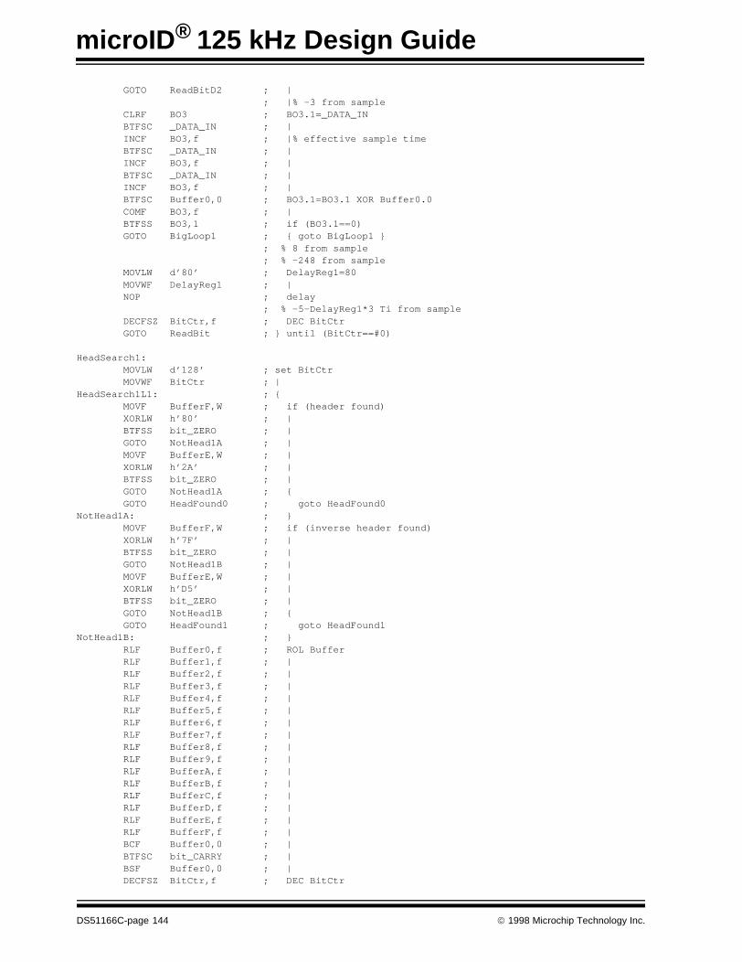
microID® 125 kHz Design Guide
GOTO ReadBitD2 ; | ; |% -3 from sample CLRF BO3 ; BO3.1=_DATA_IN BTFSC _DATA_IN ; | INCF BO3,f ; |% effective sample time BTFSC _DATA_IN ; | INCF BO3,f ; | BTFSC _DATA_IN ; | INCF BO3,f ; | BTFSC Buffer0,0 ; BO3.1=BO3.1 XOR Buffer0.0 COMF BO3,f ; | BTFSS BO3,1 ; if (BO3.1==0) GOTO BigLoop1 ; goto BigLoop1 ; % 8 from sample ; % -248 from sample MOVLW d’80’ ; DelayReg1=80 MOVWF DelayReg1 ; | NOP ; delay ; % -5-DelayReg1*3 Ti from sample DECFSZ BitCtr,f ; DEC BitCtr GOTO ReadBit ; until (BitCtr==#0)
HeadSearch1: MOVLW d’128’ ; set BitCtr MOVWF BitCtr ; |HeadSearch1L1: ; MOVF BufferF,W ; if (header found) XORLW h’80’ ; | BTFSS bit_ZERO ; | GOTO NotHead1A ; | MOVF BufferE,W ; | XORLW h’2A’ ; | BTFSS bit_ZERO ; | GOTO NotHead1A ; GOTO HeadFound0 ; goto HeadFound0NotHead1A: ; MOVF BufferF,W ; if (inverse header found) XORLW h’7F’ ; | BTFSS bit_ZERO ; | GOTO NotHead1B ; | MOVF BufferE,W ; | XORLW h’D5’ ; | BTFSS bit_ZERO ; | GOTO NotHead1B ; GOTO HeadFound1 ; goto HeadFound1NotHead1B: ; RLF Buffer0,f ; ROL Buffer RLF Buffer1,f ; | RLF Buffer2,f ; | RLF Buffer3,f ; | RLF Buffer4,f ; | RLF Buffer5,f ; | RLF Buffer6,f ; | RLF Buffer7,f ; | RLF Buffer8,f ; | RLF Buffer9,f ; | RLF BufferA,f ; | RLF BufferB,f ; | RLF BufferC,f ; | RLF BufferD,f ; | RLF BufferE,f ; | RLF BufferF,f ; | BCF Buffer0,0 ; | BTFSC bit_CARRY ; | BSF Buffer0,0 ; | DECFSZ BitCtr,f ; DEC BitCtr
DS51166C-page 144 1998 Microchip Technology Inc.

ASK Reader Reference Design
GOTO HeadSearch1L1 ; until (BitCtr==#0)
MOVF Buffer0,W ; if ((Buffer0-7)!=(Buffer8-F)) goto BigLoop1 XORWF Buffer8,W ; | BTFSS bit_ZERO ; | GOTO BigLoop1 ; | MOVF Buffer1,W ; | XORWF Buffer9,W ; | BTFSS bit_ZERO ; | GOTO BigLoop1 ; | MOVF Buffer2,W ; | XORWF BufferA,W ; | BTFSS bit_ZERO ; | GOTO BigLoop1 ; | MOVF Buffer3,W ; | XORWF BufferB,W ; | BTFSS bit_ZERO ; | GOTO BigLoop1 ; | MOVF Buffer4,W ; | XORWF BufferC,W ; | BTFSS bit_ZERO ; | GOTO BigLoop1 ; | MOVF Buffer5,W ; | XORWF BufferD,W ; | BTFSS bit_ZERO ; | GOTO BigLoop1 ; | MOVF Buffer6,W ; | XORWF BufferE,W ; | BTFSS bit_ZERO ; | GOTO BigLoop1 ; | MOVF Buffer7,W ; | XORWF BufferF,W ; | BTFSS bit_ZERO ; | GOTO BigLoop1 ; |
HeadSearch2: MOVLW d’64’ ; set BitCtr MOVWF BitCtr ; |HeadSearch2L1: ; MOVF BufferF,W ; if (header found) XORLW h’FF’ ; | BTFSS bit_ZERO ; | GOTO NotHead2A ; | BTFSS BufferE,7 ; | GOTO NotHead2A ; | BTFSC Buffer8,0 ; | GOTO NotHead2A ; GOTO HeadFound2 ; goto HeadFound2NotHead2A: ; RLF Buffer0,f ; ROL Buffer RLF Buffer1,f ; | RLF Buffer2,f ; | RLF Buffer3,f ; | RLF Buffer4,f ; | RLF Buffer5,f ; | RLF Buffer6,f ; | RLF Buffer7,f ; | RLF Buffer8,f ; | RLF Buffer9,f ; | RLF BufferA,f ; | RLF BufferB,f ; | RLF BufferC,f ; | RLF BufferD,f ; | RLF BufferE,f ; | RLF BufferF,f ; |
1998 Microchip Technology Inc. DS51166C-page 145

microID® 125 kHz Design Guide
BCF Buffer0,0 ; | BTFSC bit_CARRY ; | BSF Buffer0,0 ; | DECFSZ BitCtr,f ; DEC BitCtr GOTO HeadSearch2L1 ; until (BitCtr==#0)
HeadSearch3: MOVLW d’64’ ; set BitCtr MOVWF BitCtr ; |HeadSearch3L1: ; MOVF BufferF,W ; if (header found) XORLW h’00’ ; | BTFSS bit_ZERO ; | GOTO NotHead3A ; | BTFSC BufferE,7 ; | GOTO NotHead3A ; | BTFSS Buffer8,0 ; | GOTO NotHead3A ; GOTO HeadFound3 ; goto HeadFound3NotHead3A: ; RLF Buffer0,f ; ROL Buffer RLF Buffer1,f ; | RLF Buffer2,f ; | RLF Buffer3,f ; | RLF Buffer4,f ; | RLF Buffer5,f ; | RLF Buffer6,f ; | RLF Buffer7,f ; | RLF Buffer8,f ; | RLF Buffer9,f ; | RLF BufferA,f ; | RLF BufferB,f ; | RLF BufferC,f ; | RLF BufferD,f ; | RLF BufferE,f ; | RLF BufferF,f ; | BCF Buffer0,0 ; | BTFSC bit_CARRY ; | BSF Buffer0,0 ; | DECFSZ BitCtr,f ; DEC BitCtr GOTO HeadSearch3L1 ; until (BitCtr==#0)
GOTO BigLoop1 ; goto BigLoop1
HeadFound3: COMF BufferF,f COMF BufferE,f COMF BufferD,f COMF BufferC,f COMF BufferB,f COMF BufferA,f COMF Buffer9,f COMF Buffer8,f COMF Buffer7,f COMF Buffer6,f COMF Buffer5,f COMF Buffer4,f COMF Buffer3,f COMF Buffer2,f COMF Buffer1,f COMF Buffer0,f CALL ParityCheck BTFSC bit_CARRY GOTO BigLoop1 GOTO CheckSame
DS51166C-page 146 1998 Microchip Technology Inc.

ASK Reader Reference Design
HeadFound2: CALL ParityCheck BTFSC bit_CARRY GOTO HeadSearch3 GOTO CheckSame
HeadFound1: COMF BufferF,f COMF BufferE,f COMF BufferD,f COMF BufferC,f COMF BufferB,f COMF BufferA,f COMF Buffer9,f COMF Buffer8,f COMF Buffer7,f COMF Buffer6,f COMF Buffer5,f COMF Buffer4,f COMF Buffer3,f COMF Buffer2,f COMF Buffer1,f COMF Buffer0,fHeadFound0:
CheckSame: ; if (Buffer!=Old) goto NotSame MOVF Buffer0,W ; | XORWF Old0,W ; | BTFSS bit_ZERO ; | GOTO NotSame ; | MOVF Buffer1,W ; | XORWF Old1,W ; | BTFSS bit_ZERO ; | GOTO NotSame ; | MOVF Buffer2,W ; | XORWF Old2,W ; | BTFSS bit_ZERO ; | GOTO NotSame ; | MOVF Buffer3,W ; | XORWF Old3,W ; | BTFSS bit_ZERO ; | GOTO NotSame ; | MOVF Buffer4,W ; | XORWF Old4,W ; | BTFSS bit_ZERO ; | GOTO NotSame ; | MOVF Buffer5,W ; | XORWF Old5,W ; | BTFSS bit_ZERO ; | GOTO NotSame ; | MOVF Buffer6,W ; | XORWF Old6,W ; | BTFSS bit_ZERO ; | GOTO NotSame ; | MOVF Buffer7,W ; | XORWF Old7,W ; | BTFSS bit_ZERO ; | GOTO NotSame ; | MOVF Buffer8,W ; | XORWF Old8,W ; | BTFSS bit_ZERO ; | GOTO NotSame ; | MOVF Buffer9,W ; | XORWF Old9,W ; | BTFSS bit_ZERO ; |
1998 Microchip Technology Inc. DS51166C-page 147

microID® 125 kHz Design Guide
GOTO NotSame ; | MOVF BufferA,W ; | XORWF OldA,W ; | BTFSS bit_ZERO ; | GOTO NotSame ; | MOVF BufferB,W ; | XORWF OldB,W ; | BTFSS bit_ZERO ; | GOTO NotSame ; | MOVF BufferC,W ; | XORWF OldC,W ; | BTFSS bit_ZERO ; | GOTO NotSame ; | MOVF BufferD,W ; | XORWF OldD,W ; | BTFSS bit_ZERO ; | GOTO NotSame ; | MOVF BufferE,W ; | XORWF OldE,W ; | BTFSS bit_ZERO ; | GOTO NotSame ; | MOVF BufferF,W ; | XORWF OldF,W ; | BTFSS bit_ZERO ; | GOTO NotSame ; |
Same:
TxTag: ;- Transmit tag BSF _LED2 ; LEDs “Found tag” CALL Delay07 ; | BCF _LED1 ; | MOVLW d’4’ ; Beep at 3597Hz for 1024 cycles MOVWF BeepCtrHi ; | MOVLW d’0’ ; | MOVWF BeepCtrLo ; |BeepLoopJ1: ; | GOTO BeepLoopJ2 ; |BeepLoopJ2: ; | MOVLW Beep1 ; | MOVWF BeepPort ; | MOVLW d’34’ ; | MOVWF DelayReg1 ; |BeepD1: ; | CLRWDT ; | DECFSZ DelayReg1,f ; | GOTO BeepD1 ; | MOVLW Beep2 ; | MOVWF BeepPort ; | MOVLW d’32’ ; | MOVWF DelayReg1 ; | NOP ; | GOTO BeepD2 ; |BeepD2: ; | CLRWDT ; | DECFSZ DelayReg1,f ; | GOTO BeepD2 ; | DECFSZ BeepCtrLo,f ; | GOTO BeepLoopJ1 ; | DECFSZ BeepCtrHi,f ; | GOTO BeepLoopJ2 ; | NOP ; | MOVLW Beep0 ; | MOVWF BeepPort ; |
MOVF OldF,W
DS51166C-page 148 1998 Microchip Technology Inc.

ASK Reader Reference Design
MOVWF BufferF MOVF OldE,W MOVWF BufferE MOVF OldD,W MOVWF BufferD MOVF OldC,W MOVWF BufferC MOVF OldB,W MOVWF BufferB MOVF OldA,W MOVWF BufferA MOVF Old9,W MOVWF Buffer9 MOVF Old8,W MOVWF Buffer8 MOVF Old7,W MOVWF Buffer7 MOVF Old6,W MOVWF Buffer6 MOVF Old5,W MOVWF Buffer5 MOVF Old4,W MOVWF Buffer4 MOVF Old3,W MOVWF Buffer3 MOVF Old2,W MOVWF Buffer2 MOVF Old1,W MOVWF Buffer1 MOVF Old0,W MOVWF Buffer0
CALL RS232CR ; Transmit tag info MOVLW ‘A’ ; | CALL RS232TxW ; | MOVLW ‘S’ ; | CALL RS232TxW ; | MOVLW ‘K’ ; | CALL RS232TxW ; | CALL RS232CR ; | MOVLW ‘T’ ; | CALL RS232TxW ; | MOVLW ‘b’ ; | CALL RS232TxW ; | MOVLW ‘i’ ; | CALL RS232TxW ; | MOVLW ‘t’ ; | CALL RS232TxW ; | MOVLW ‘=’ ; | CALL RS232TxW ; | MOVLW ‘6’ ; | CALL RS232TxW ; | MOVLW ‘4’ ; | CALL RS232TxW ; | MOVLW ‘T’ ; | CALL RS232TxW ; | MOVLW ‘c’ ; | CALL RS232TxW ; | MOVLW ‘y’ ; | CALL RS232TxW ; | CALL RS232CR ; | MOVLW ‘C’ ; | CALL RS232TxW ; | MOVLW ‘o’ ; | CALL RS232TxW ; |
1998 Microchip Technology Inc. DS51166C-page 149

microID® 125 kHz Design Guide
MOVLW ‘n’ ; | CALL RS232TxW ; | MOVLW ‘s’ ; | CALL RS232TxW ; | MOVLW ‘t’ ; | CALL RS232TxW ; | MOVLW ‘a’ ; | CALL RS232TxW ; | MOVLW ‘n’ ; | CALL RS232TxW ; | MOVLW ‘t’ ; | CALL RS232TxW ; | CALL RS232CR ; | MOVLW ‘T’ ; | CALL RS232TxW ; | MOVLW ‘t’ ; | CALL RS232TxW ; | MOVLW ‘a’ ; | CALL RS232TxW ; | MOVLW ‘g’ ; | CALL RS232TxW ; | MOVLW ‘=’ ; | CALL RS232TxW ; | MOVF BufferF,W ; | XORLW h’80’ ; | BTFSS bit_ZERO ; | GOTO Ttag64 ; |Ttag128: ; | MOVLW ‘1’ ; | CALL RS232TxW ; | MOVLW ‘2’ ; | CALL RS232TxW ; | MOVLW ‘8’ ; | CALL RS232TxW ; | GOTO TtagJ1 ; |Ttag64: ; | MOVLW ‘6’ ; | CALL RS232TxW ; | MOVLW ‘4’ ; | CALL RS232TxW ; | GOTO TtagJ1 ; |TtagJ1: ; | MOVLW ‘T’ ; | CALL RS232TxW ; | MOVLW ‘b’ ; | CALL RS232TxW ; | MOVLW ‘i’ ; | CALL RS232TxW ; | MOVLW ‘t’ ; | CALL RS232TxW ; | CALL RS232CR ; | MOVLW ‘P’ ; | CALL RS232TxW ; | MOVLW ‘o’ ; | CALL RS232TxW ; | MOVLW ‘l’ ; | CALL RS232TxW ; | MOVLW ‘a’ ; | CALL RS232TxW ; | MOVLW ‘r’ ; | CALL RS232TxW ; | MOVLW ‘i’ ; | CALL RS232TxW ; | MOVLW ‘t’ ; | CALL RS232TxW ; | MOVLW ‘y’ ; |
DS51166C-page 150 1998 Microchip Technology Inc.

ASK Reader Reference Design
CALL RS232TxW ; | MOVLW ‘ ‘ ; | CALL RS232TxW ; | MOVLW ‘0’ ; | CALL RS232TxW ; | CALL RS232CR ; | MOVLW BufferF ; Transmit tag ID MOVWF FSR ; | MOVF BufferF,W ; | XORLW h’80’ ; | BTFSC bit_ZERO ; | GOTO TxLoop1 ; | MOVLW Buffer7 ; | MOVWF FSR ; |TxLoop1: ; | SWAPF INDF,W ; | CALL RS232TxDigit ; | MOVF INDF,W ; | CALL RS232TxDigit ; | DECF FSR,f ; | BTFSC FSR,4 ; | GOTO TxLoop1 ; | CALL RS232CR ; |
GOTO BigLoop1 ; goto BigLoop1
NotSame: ; Old=Data MOVF Buffer0,W ; | MOVWF Old0 ; | MOVF Buffer1,W ; | MOVWF Old1 ; | MOVF Buffer2,W ; | MOVWF Old2 ; | MOVF Buffer3,W ; | MOVWF Old3 ; | MOVF Buffer4,W ; | MOVWF Old4 ; | MOVF Buffer5,W ; | MOVWF Old5 ; | MOVF Buffer6,W ; | MOVWF Old6 ; | MOVF Buffer7,W ; | MOVWF Old7 ; | MOVF Buffer8,W ; | MOVWF Old8 ; | MOVF Buffer9,W ; | MOVWF Old9 ; | MOVF BufferA,W ; | MOVWF OldA ; | MOVF BufferB,W ; | MOVWF OldB ; | MOVF BufferC,W ; | MOVWF OldC ; | MOVF BufferD,W ; | MOVWF OldD ; | MOVF BufferE,W ; | MOVWF OldE ; | MOVF BufferF,W ; | MOVWF OldF ; | GOTO BigLoop1 ; goto BigLoop1
end
1998 Microchip Technology Inc. DS51166C-page 151

microID® 125 kHz Design Guide
NOTES:
DS51166C-page 152 1998 Microchip Technology Inc.

FSK Anti-Collision Reader Reference Design
FSK Anti-Collision Reader Reference Design
1.0 INTRODUCTIONWhen more than one tag is in the same RF field of areader, each tag will transmit data at the same time.This results in data collision at the receiving end of thereader. No correct decision can be made based on thisdata. The reader must receive data from a tag at a timefor correct data processing.
The anti-collision device (MCRF250) is designed tosend FSK data to reader without data collision, and itmust be read by an anti-collision reader. This type ofdevice can be effectively used in inventory and assetcontrol applications where multiple tags are read in thesame RF field. The anti-collision algorithm of the deviceis explained in the MCRF250 Data Sheet (DS21267).
This application note is written as a reference guide foranti-collision reader designers. The anti-collisionreader is designed to provide correct signals to the anti-collision device (MCRF250) to perform an anti-collisionaction during operation.
Microchip Technology Inc. provides basic anti-collisionFSK reader electronic circuitry for the MCRF250customers as a part of this design guide. The microIDAnti-collision Reader (demo unit), that can read 10 tagsor more in the same RF field, is available in the microIDDevelopers Kit (DV103002). An electronic copy of themicroID PICmicro® source code is also available uponrequest.
FIGURE 1-1: BLOCK DIAGRAM OF TYPICAL RFID READER FOR FSK SIGNAL (125 kHz)
(4 MHz Crystal Oscillator)Carrier Signal Amplifier
(Power Driver)
Envelope Detector
Interface with Host Computer
Transmitting Section
Antenna Coil
CLK
To Host ComputerSerial Interface (RS-232)
125 kHz
Time Base Signal Generator
Microcontroller
Data Decoding
Receiving Section
÷ 32
Signal Collision Detector
Gap Signal Gate
Filter/AmplifierPulse Waveform Shaping Data
1998 Microchip Technology Inc. DS51167B-page 153
PICmicro is a registered tradmark of Microchip Technology Inc.

microID® 125 kHz Design Guide
2.0 READER CIRCUITSThe anti-collision RFID reader consists of atransmitting and a receiving section. The transmittingsection includes a carrier frequency generator, gapsignal gate, and an antenna circuit. The receivingsection includes peak detector, signal amplifier/filter,signal collision detector, and the microcontroller fordata processing.
The reader also communicates with an external hostcomputer. A basic block diagram of the typical RFIDreader is shown in Figure 1-1.
The electronic circuitry for an anti-collision FSK readeris shown in Section 3.0. The reader needs a +9 VDC
power supply.
The 125 kHz carrier signal is generated by dividing the4 MHz time base signal that is generated by a crystaloscillator. A 16-stage binary ripple counter (74HC4060)is used for this purpose. The 74HC4060 also providesa clock signal for the PIC16C84 microcontroller. The125 kHz signal from Pin no. 5 of U6 is fed into U2 (Norgate) and two stage power amplifiers that are formedby U4, Q1, and Q2.
The 125 kHz signal from Q1 and Q2 is fed into theantenna circuit formed by L1(1.62 mH) and C22 (1000pF). L1 and C22 form a series resonant circuit for a 125kHz resonance frequency. Since the C22 is grounded,the carrier signal (125 kHz) is filtered out to groundafter passing the antenna coil. The circuit provides aminimum impedance at the resonance frequency. Thisresults in maximizing the antenna current, andtherefore, the magnetic field strength is maximized.
The gap signal from Pin no. 7 of U7 (Microcontroller)controls the 125 KHz antenna driver circuit (Q1 andQ2). Q1 and Q2 are turned off during the gap signal“high”. There is no RF signal at the antenna coil duringthis gap period.
The reader circuit uses a single coil for both transmit-ting and receiving signals. L1, C22, D8, and the othercomponents in the bottom parts of the circuit form a sig-nal receiving section.
In the FSK communication protocol, a ‘0’ and a ‘1’ arerepresented by two different frequencies. In theMCRF250, a ‘0’ and a ‘1’ are represented by Fc/8 andFc/10, respectively. Fc is the carrier frequency. TheMCRF250 sends this FSK signal to the reader by anamplitude modulation of the carrier signal.
The demodulation is accomplished by detecting theenvelope of the carrier signal. A half-wavecapacitor-filtered rectifier circuit (D8, D9, and C26) isused for the demodulation process. The detected enve-lope signal is charged into the C26. R37 provides a dis-charge path for the voltage charged in the C26. Thisvoltage passes active filters (U10:A,C,D) and the pulseshaping circuitry (U10:B) before it is fed into thePIC16C84 for data processing. U10 (A,D,C) forms abandpass filter for 12 kHz – 16 kHz signals.
When more than one tag are transmitting data at sametime, there will be wobbles in data signals in thereceiver. This wobble is detected in U8. If the wobbleoccurs, c10 becomes fully charged. This will set CLKinput of US:B, and results in a logic “LOW” in Q of theU5:B. The microcontoller (U7) detects the logic “LOW”and turns on the gap control gate (U5:A) to send a gapsignla to the tags.
The PIC16C84 microcontroller performs data decod-ing, provides gap timing signals, and communicateswith the host computer via an RS-232 serial interface.
FIGURE 2-1: RFID FSK ANTI-COLLISION WINDOW
DS51167B-page 154 1998 Microchip Technology Inc.

FSK Anti-Collision Reader Reference Design
FIGURE 2-2: ANTI-COLLISION ALGORITHM FOR A MCRF250 READER
Modulation
Gap Carrier
Wait 5 bit times
Field On
Yes
No
Present?
60 µSec
Gap Carrier 60 µSec
Modulation Present?
Data
Read
Collision?
tag data
Verify Headerand Data?
Gap Carrier1st half bit 1
YesNo
No
Yes
No
Yes
1998 Microchip Technology Inc. DS51167B-page 155

microID® 125 kHz Design Guide
3.0 ANTI-COLLISION READER SCHEMATIC
D7
1N41
48
D5
1N41
48
C27
470u
F, 1
6V
1N49
36
D8
U10
:B7
+5
-6
MC
3408
4U10
:A
1
+3
-2
+5V
Q1
IRF
9520
Q4
2N70
00
U2:
B
465
U2:
D
1 3
1 21 1
U9:
A
4013
Q2
Q1
RE
SE
T4
CLK
3D
5S
ET
6
U5:
B
4013
Q12
Q13
RE
SE
T10
CLK
11D
9S
ET
8
+5V
D2
1N41
48
U4
ICL7
667
IN2
4
VS
S3
IN1
2
NC
1N
C8
OU
T1
7
VD
D6
OU
T2
5
1N49
36
D1
10uF
C5
IRF
740
Q2
R15
820
R10
33K
MC
3408
4
U8:
A1
+3
-2
MC
3408
4
U8:
B
7
+5
-6
MC
3408
4
U8:
C 8
+10
-9
U10
:C8
+10
-9
U10
:D14
+12
-13
0.1u
F
C9
R4
1M
R6
100K
C8 0.1u
F
1000
pF,5
%
C7
R8
150k
33K
R9
1000
pF,5
%
C6
L1
162u
Hy
+5V
R20
820
R17
33K
150K
R19
1000
pF,5
%
C13
C15
1000
pF,5
%
C22
0.01
uF,6
30V
1000
pF,5
%
C12
1000
pF,5
%
C14
150K
R18
R22
1.82
K,1
%
R21
33K
R24
820
1N4936
D9
74HC4060
U6
CK
I11
CLR
12C
KO
10
CK
O9
QD
7
QE
5
QF
4
QG
6
QH
14
QI
13
QJ
15
QL
1
QM
2
QN
3
R2
1M
330
R1
C2
22
4.0
0 M
Hz
Y1
10uF,16V
C3+5V
U3
5VVO
3G 2
VI
1
470uF,16V
C4
R3
10K
2N29
07
Q3
2.67
K,1
%
R23
1000
pF,5
%
C16
R27
47.5
K,1
%
.0022uF,200V,10%
C26390K
R35
C24
1000
pF,2
00V
,5%
R29
82.5
K,1
%
C21
1000pF,5%
C19
1000pF,5%
10K,1%
R34
C23
1000pF,5%
R32
10K,5%
R26
10K 1%
1000
pF,5
%
C25
R33
10K,1%
+5V
1N4148
D3
1N4148
D6
R11
22K
100K
R14
R5
3.3K
R7
1.8KU
7R
A2
1
RA
32
RT
CC
3
MC
LR4
VS
S5
RB
06
RB
17
RB
28
RB
39
RB
410
RB
511
RB
612
RB
713
VD
D14
CK
OU
T15
RA
017
RA
118
CLK
IN16
330
R16
330
R13
P1
R31
1M,5%
6.8K
R25 R30
220,5%
R28
15K
0.1uF
C18
1000
pF,5
%
C17
C20
10uf
,16V
C11
0.1u
F
.47uF
C10D4
1N41
4810
K
R12
4013
U9:
B SE
T8
D9
CLK
11
RE
SE
T10
Q13
Q12
SP
1C
1
22
U5:
A
4013
Q2
Q1
RE
SE
T4
CLK
3D
5S
ET
6
U8:
D
MC
3408
4
-13
+12
14
LED
1
AR
ED
AG
RN
U2:
A1
32
U2:
C
1098
U1
12V
LM78
L12A
CZ
A
VO
3G
2
VI
1
PIC
16F
84
+9-1
5V
out
ingn
d
RS-232
4 11
* O
nly
stuf
f thi
s pa
rt fo
rus
e w
ith a
15V
sup
ply.
*
DS51167B-page 156 1998 Microchip Technology Inc.

FSK Anti-Collision Reader Reference Design
4.0 ANTI-COLLISION READER BILL OF MATERIALSQuantity Type Value Reference Designator Part Number
1 PIEZO Buzzer PKM17EPP-4001 BZ1 MURATA PART #
2 Capacitor 22 pF C1, C2 1330PH-ND
12 Capacitor lOOO pF, 5% C6,C7,C12,C13,C14C15,C16, C17,C19,C21,C23,C25
P4937-ND
1 Capacitor 1000 pF, 200V, 5% C24 (P3497-ND)
1 Capacitor .0022 µF, 200V, 10% C26 P3S01-ND
1 Capacitor 0.01µF, 630V c22 P3509-ND
4 Capacitor 0.1 µF C8, C9, C11, C18 P4539-ND
1 Capacitor 0.47 µF C10 P4967-ND
3 Capacitor 10 µF, 16V C3, C5, C20 P6616-ND
1 Capacitor l00 µF, 25V C4 P10269-ND
1 Capacitor 470 µF, 16V C27 P10247-ND
6 Diode 1N4148 D2, D3, D4, D5, D6, D7 1N4148DICT-ND
3 Diode 1N4936 D1, DB, D9 1N4936CT-ND
1 Bicolor LED P392 LED 1 p392-ND
1 Coil Antenna 162 uBy L1 Custom Wound
1 P-Chain MOSFET IRF9520 Q1 IRF9520 FUTURE
1 N-Chain MOSFET IRF740 Q2 IRF740-ND
1 PNP Transistor 2N2907 Q3 PN2907A-ND
1 N-Chain MOSFET 2N7000 Q4 2N7000DICT-ND
1 Resistor 220, 5% R30 5043CX220ROJ
3 Resistor 330, 5% R1, R13, R16 5043CX330ROJ
3 Resistor 820, 5% R15, R20, R24 5043CX830ROJ
Resistor 1.8K, 5% R7 1K8CR-1/4W-B 5%
1 Resistor 1.82K, 1% R22 1K82MF-1/4W-B 5%
1 Resistor 2.67K, 15 R23 2K67MF-1/4W-B 1%
1 Resistor 3.3K, 5% R5 3K3CR-1/4W-B 5%
1 Resistor 6.8K, 5% R25 6K8CR-1/4W-B 5%
3 Resistor 10R,1’ R26, R33, R34 5043ED10KOOF
3 Resistor 10K, 5% R3, R12, R32 10KCR-1/4W-B 5%
1 Resistor 15K, 5% R28 15KCR-1/4W-B 5%
1 Resistor 22K, 5% R11 22KCR-1/4W-B 5%
4 Resistor 33K, 5% R9,R10, R17, R21 33JCR1/4-B 5%
1 Resistor 47.5K, 1% R27 47K5MF-1/4W-B 1%
1 Resistor 82.5K, 1% R29 82.5KMF-1/4W-B 1%
2 Resistor 100K, 5% R6, R14 5043CX100KOJ
3 Resistor 150K, 5% R8, R18, R19 150KCR-1/4W-B 5%
1 Resistor 390K, 5% R35 390KCR-1/4-B, 5%
3 Resistor 1M, 5% R2, R4, R31 1MOCR-1/4W-B 5%
1 QUAD NOR GATE 74HC02 U2 MM74HC02N-ND
1 5V Regulator LM78L05 U3 NJM78L05A-ND
1 MOSFET Driver ICL7667 U4 ICL7667CPA-ND
2 DUAL FLIP-FLOP 4013 U5, U9 CD4013BCN-ND
Note: All resistors are 5% 1/4 watt carbon film resistors unless otherwise noted. DIGI-KEY part numbers follow some parts where applicable (these part numbers are only intended as a reference).
1998 Microchip Technology Inc. DS51167B-page 157

microID® 125 kHz Design Guide
1 Binary Counter 74HC4060 U6 MM74HC4060N-ND
1 Microprocessor PIC16F84 U7 PIC16F84-04/P
2 OP-AMP MC3407 U8, U10 FUTURE PART #
1 Crystal 4.00 MHz Y1 X405-ND
Quantity Type Value Reference Designator Part Number
Note: All resistors are 5% 1/4 watt carbon film resistors unless otherwise noted. DIGI-KEY part numbers follow some parts where applicable (these part numbers are only intended as a reference).
DS51167B-page 158 1998 Microchip Technology Inc.

FSK Anti-Collision Reader Reference Design
5.0 FSK ANTI-COLLISION SOURCE CODE FOR THE PICmicro® MCU The following source code is for the PIC16C84 microcontroller used in the FSK reader electronics.
; #=#=#=#=#=#=#=# PROJECT Microchip FSK anticollision Reader #=#=#=#=#=#=#=#; v008.asm; PIC16F84 running at 4MHz, Ti=1us
; ///////////////////////////////////////////////////////////////////////////; Revision history; ///////////////////////////////////////////////////////////////////////////;; Ver Date Comment;; 0.01 29 Dec 97 Copied from MChip\Reader\FSK; 0.02 27 Feb 98 Gap during first half of first bit; 0.05 28 Apr 98 Change from PIC16C84 to PIC16F84; 0.06 29 Apr 98 Count to 256 instead of to 512; 0.07 30 Apr 98 Make PORTB.0 low output (previously demodulated data input); 0.07a 08 May 98 Make gaps 80us wide; 0.08 13 Aug 98 TAKE OUT CODE INTENDED FOR LAB USE ONLY;; Tbit=50Tcy=400Ti; Ttag=96Tbit; Header=h’802A’;
processor pic16f84#include “p16f84.inc”
__config b’00000000000001’ ; Code Protect on, power-up timer on, WDT off, XT oscillator
#define _CARRY STATUS,0#define _ZERO STATUS,2#define _TO STATUS,4#define _RP0 STATUS,5#define _PAGE0 PCLATH,3
#define _BUZZ1 PORTA,0#define _BUZZ2 PORTA,1#define _RS232TX PORTA,2#define _RS232RX PORTA,3#define _SDA PORTA,4StartPORTA = b’11100’StartTRISA = b’01000’BeepPort = PORTABeep0 = StartPORTABeep1 = StartPORTA | b’00001’Beep2 = StartPORTA | b’00010’
#define _UNUSED1 PORTB,0#define _COIL_PWR PORTB,1#define _LED1 PORTB,2#define _LED2 PORTB,3#define _RAW_DATA PORTB,4#define _UNUSED2 PORTB,5#define _COLLISION PORTB,6 ; < Goes low when a collision occurs#define _SCL PORTB,7StartPORTB = b’10000010’ ; Coil_OffStartTRISB = b’01010000’
StartOPTION = b’10001111’; PORTB pullups disabled, TMR0 internal, prescaler off, WDT/256
BO3 = h’0C’ ; Could be doubled-up with DelayReg1DelayReg1 = h’0D’ ; Could be doubled-up with BO3
1998 Microchip Technology Inc. DS51167B-page 159
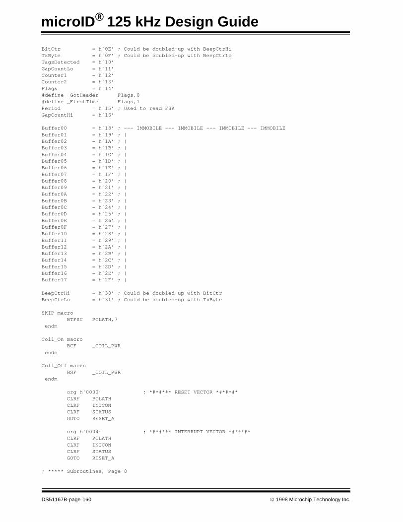
microID® 125 kHz Design Guide
BitCtr = h’0E’ ; Could be doubled-up with BeepCtrHiTxByte = h’0F’ ; Could be doubled-up with BeepCtrLoTagsDetected = h’10’GapCountLo = h’11’Counter1 = h’12’Counter2 = h’13’Flags = h’14’#define _GotHeader Flags,0#define _FirstTime Flags,1Period = h’15’ ; Used to read FSKGapCountHi = h’16’
Buffer00 = h’18’ ; --- IMMOBILE --- IMMOBILE --- IMMOBILE --- IMMOBILEBuffer01 = h’19’ ; |Buffer02 = h’1A’ ; |Buffer03 = h’1B’ ; |Buffer04 = h’1C’ ; |Buffer05 = h’1D’ ; |Buffer06 = h’1E’ ; |Buffer07 = h’1F’ ; |Buffer08 = h’20’ ; |Buffer09 = h’21’ ; |Buffer0A = h’22’ ; |Buffer0B = h’23’ ; |Buffer0C = h’24’ ; |Buffer0D = h’25’ ; |Buffer0E = h’26’ ; |Buffer0F = h’27’ ; |Buffer10 = h’28’ ; |Buffer11 = h’29’ ; |Buffer12 = h’2A’ ; |Buffer13 = h’2B’ ; |Buffer14 = h’2C’ ; |Buffer15 = h’2D’ ; |Buffer16 = h’2E’ ; |Buffer17 = h’2F’ ; |
BeepCtrHi = h’30’ ; Could be doubled-up with BitCtrBeepCtrLo = h’31’ ; Could be doubled-up with TxByte
SKIP macro BTFSC PCLATH,7 endm
Coil_On macro BCF _COIL_PWR endm
Coil_Off macro BSF _COIL_PWR endm
org h’0000’ ; *#*#*#* RESET VECTOR *#*#*#* CLRF PCLATH CLRF INTCON CLRF STATUS GOTO RESET_A
org h’0004’ ; *#*#*#* INTERRUPT VECTOR *#*#*#* CLRF PCLATH CLRF INTCON CLRF STATUS GOTO RESET_A
; ***** Subroutines, Page 0
DS51167B-page 160 1998 Microchip Technology Inc.

FSK Anti-Collision Reader Reference Design
Delay10: ;[0] Delay 10Ti GOTO Delay08 ; |Delay08: ;[0] Delay 8Ti GOTO Delay06 ; |Delay06: ;[0] Delay 6Ti NOP ; |Delay05: ;[0] Delay 5Ti NOP ; |Delay04: ;[0] Delay 4Ti RETLW 0 ; |
;%% CALL RS232CR takes 1052Ti;%% CALL RS232TxDigit takes 1057Ti;%% CALL RS232TxW takes 1049TiRS232CR: ;[1] Transmit CR on RS232 MOVLW d’13’ ; | GOTO RS232TxW ; |RS232TxDigit: ;[1] Transmit LSnybble of W on RS232 ANDLW h’0F’ ; | MOVWF TxByte ; | MOVLW h’A’ ; | SUBWF TxByte,W ; | MOVLW ‘0’ ; | BTFSC _CARRY ; | MOVLW ‘A’-h’A’ ; | ADDWF TxByte,W ; |RS232TxW: ;[1] Transmit W on RS232 at 9615 baud MOVWF TxByte ; | TxByte=WRS232Tx: ;[1] Transmit TxByte - 104us = 9615.4 baud BSF _RS232TX ; | Stop bit MOVLW d’35’ ; | | Delay 106Ti MOVWF DelayReg1 ; | | |RS232TxD1: ; | | | DECFSZ DelayReg1,f ; | | | GOTO RS232TxD1 ; | | | BCF _RS232TX ; | Start bit NOP ; | | Delay 98Ti MOVLW d’32’ ; | | | MOVWF DelayReg1 ; | | |RS232TxD2: ; | | | DECFSZ DelayReg1,f ; | | | GOTO RS232TxD2 ; | | | CLRF BitCtr ; | BitCtr=#8 BSF BitCtr,3 ; | |RS232TxL1: ; | % -4Ti BTFSC TxByte,0 ; | Transmit TxByte.0, RR TxByte GOTO RS232TxBit1 ; | | NOP ; | |RS232TxBit0: ; | | BCF _RS232TX ; | | BCF _CARRY ; | | GOTO RS232TxBitDone ; | |RS232TxBit1: ; | | BSF _RS232TX ; | | BSF _CARRY ; | | GOTO RS232TxBitDone ; | |RS232TxBitDone: ; | | RRF TxByte,f ; | |% 4Ti MOVLW d’30’ ; | Delay 93Ti MOVWF DelayReg1 ; | | GOTO RS232TxD3 ; | |RS232TxD3: ; | | DECFSZ DelayReg1,f ; | | GOTO RS232TxD3 ; | | DECFSZ BitCtr,f ; | DEC BitCtr
1998 Microchip Technology Inc. DS51167B-page 161

microID® 125 kHz Design Guide
GOTO RS232TxL1 ; | until (BitCtr==#0) CALL Delay04 ; | Delay 4Ti BSF _RS232TX ; | stop bit RETLW 0 ; end
DelayTtag: ;[?] Delay Ttag-3Ti=38400-3Ti=38397Ti BSF _PAGE0 GOTO P1DelayTtag
; ***** End of subroutines, Page 0
RESET_A: CLRWDT ; Initialise registers CLRF STATUS ; | Access register page 0 CLRF FSR ; | FSR=#0 MOVLW StartPORTA ; | Initialise PORT and TRIS registers MOVWF PORTA ; | | MOVLW StartPORTB ; | | MOVWF PORTB ; | | BSF _RP0 ;^| | MOVLW StartTRISA ;^| | MOVWF TRISA ;^| | MOVLW StartTRISB ;^| | MOVWF TRISB ;^| | BCF _RP0 ; | Initialise OPTION register MOVLW StartOPTION ; | | CLRF TMR0 ; | | BSF _RP0 ;^| | MOVWF OPTION_REG ;^| | BCF _RP0 ; | |
BigLoop1: CALL Delay08 ; LEDs “reading” BSF _LED1 ; | CALL Delay08 ; | BCF _LED2 ; | CALL Delay08 ; | Coil_Off ; Turn coil off
BSF _PAGE0 GOTO ResetDelayResetDelayDone:
CLRF TagsDetected ; TagsDetected=#0 CLRF GapCountHi ; GapCount=#0 CLRF GapCountLo ; |GapLoop: ; Coil_Off ; Turn coil off CALL Delay08 ; LEDs “reading” BSF _LED1 ; | CALL Delay08 ; | BCF _LED2 ; | CALL Delay10 ; Wait 80us CALL Delay10 ; | CALL Delay10 ; | CALL Delay10 ; | CALL Delay10 ; | CALL Delay10 ; | NOP ; | Coil_On ; Turn coil on ;% 0 Ti from 1st bit
;(Ttag=38400Ti); If it’s the first gap since reset, delay Ttag
DS51167B-page 162 1998 Microchip Technology Inc.
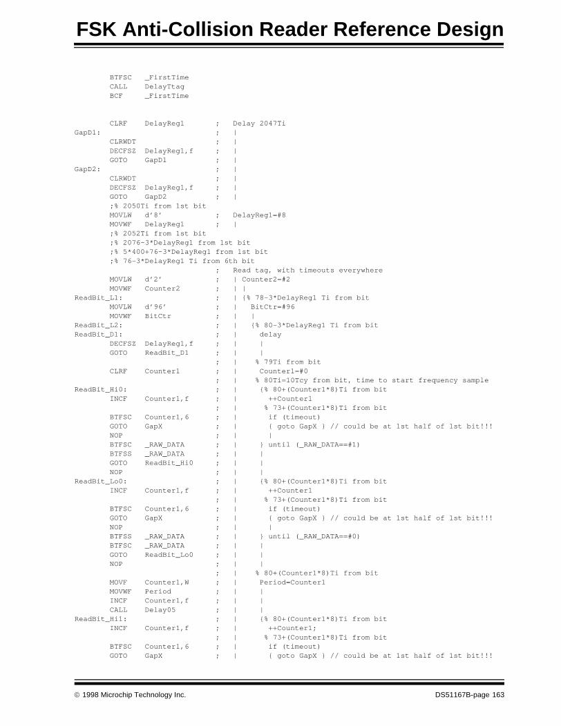
FSK Anti-Collision Reader Reference Design
BTFSC _FirstTime CALL DelayTtag BCF _FirstTime
CLRF DelayReg1 ; Delay 2047TiGapD1: ; | CLRWDT ; | DECFSZ DelayReg1,f ; | GOTO GapD1 ; |GapD2: ; | CLRWDT ; | DECFSZ DelayReg1,f ; | GOTO GapD2 ; | ;% 2050Ti from 1st bit MOVLW d’8’ ; DelayReg1=#8 MOVWF DelayReg1 ; | ;% 2052Ti from 1st bit ;% 2076-3*DelayReg1 from 1st bit ;% 5*400+76-3*DelayReg1 from 1st bit ;% 76-3*DelayReg1 Ti from 6th bit ; Read tag, with timeouts everywhere MOVLW d’2’ ; | Counter2=#2 MOVWF Counter2 ; | |ReadBit_L1: ; | % 78-3*DelayReg1 Ti from bit MOVLW d’96’ ; | BitCtr=#96 MOVWF BitCtr ; | |ReadBit_L2: ; | % 80-3*DelayReg1 Ti from bitReadBit_D1: ; | delay DECFSZ DelayReg1,f ; | | GOTO ReadBit_D1 ; | | ; | % 79Ti from bit CLRF Counter1 ; | Counter1=#0 ; | % 80Ti=10Tcy from bit, time to start frequency sampleReadBit_Hi0: ; | % 80+(Counter1*8)Ti from bit INCF Counter1,f ; | ++Counter1 ; | % 73+(Counter1*8)Ti from bit BTFSC Counter1,6 ; | if (timeout) GOTO GapX ; | goto GapX // could be at 1st half of 1st bit!!! NOP ; | | BTFSC _RAW_DATA ; | until (_RAW_DATA==#1) BTFSS _RAW_DATA ; | | GOTO ReadBit_Hi0 ; | | NOP ; | |ReadBit_Lo0: ; | % 80+(Counter1*8)Ti from bit INCF Counter1,f ; | ++Counter1 ; | % 73+(Counter1*8)Ti from bit BTFSC Counter1,6 ; | if (timeout) GOTO GapX ; | goto GapX // could be at 1st half of 1st bit!!! NOP ; | | BTFSS _RAW_DATA ; | until (_RAW_DATA==#0) BTFSC _RAW_DATA ; | | GOTO ReadBit_Lo0 ; | | NOP ; | | ; | % 80+(Counter1*8)Ti from bit MOVF Counter1,W ; | Period=Counter1 MOVWF Period ; | | INCF Counter1,f ; | | CALL Delay05 ; | |ReadBit_Hi1: ; | % 80+(Counter1*8)Ti from bit INCF Counter1,f ; | ++Counter1; ; | % 73+(Counter1*8)Ti from bit BTFSC Counter1,6 ; | if (timeout) GOTO GapX ; | goto GapX // could be at 1st half of 1st bit!!!
1998 Microchip Technology Inc. DS51167B-page 163

microID® 125 kHz Design Guide
NOP ; | | BTFSC _RAW_DATA ; | until (_RAW_DATA==#1) BTFSS _RAW_DATA ; | | GOTO ReadBit_Hi1 ; | | NOP ; | |ReadBit_Lo1: ; | % 80+(Counter1*8)Ti from bit INCF Counter1,f ; | ++Counter1; ; | % 73+(Counter1*8)Ti from bit BTFSC Counter1,6 ; | if (timeout) GOTO GapX ; | goto GapX // could be at 1st half of 1st bit!!! NOP ; | | BTFSS _RAW_DATA ; | until (_RAW_DATA==#0) BTFSC _RAW_DATA ; | | GOTO ReadBit_Lo1 ; | | NOP ; | |ReadBit_Hi2: ; | % 80+(Counter1*8)Ti from bit INCF Counter1,f ; | ++Counter1; ; | % 73+(Counter1*8)Ti from bit BTFSC Counter1,6 ; | if (timeout) GOTO GapX ; | goto GapX // could be at 1st half of 1st bit!!! NOP ; | | BTFSC _RAW_DATA ; | until (_RAW_DATA==#1) BTFSS _RAW_DATA ; | | GOTO ReadBit_Hi2 ; | | NOP ; | |ReadBit_Lo2: ; | % 80+(Counter1*8)Ti from bit INCF Counter1,f ; | ++Counter1; ; | % 73+(Counter1*8)Ti from bit BTFSC Counter1,6 ; | if (timeout) GOTO GapX ; | goto GapX // could be at 1st half of 1st bit!!! NOP ; | | BTFSS _RAW_DATA ; | until (_RAW_DATA==#0) BTFSC _RAW_DATA ; | | GOTO ReadBit_Lo2 ; | | NOP ; | | ; | % 80+(Counter1*8)Ti from bit MOVF Period,W ; | Period=Counter1-Period SUBWF Counter1,W ; | | MOVWF Period ; | | ; | % 83+(Counter1*8)Ti from bit COMF Counter1,W ; | W=32-Counter1 ADDLW d’1’ ; | | ADDLW d’32’ ; | | ; | % 86+(32-W)*8Ti from bit ; | % 86+(Counter1*8)Ti from bit INCF Counter1,f ; | ++Counter1 INCF Counter1,f ; | ++Counter1 NOP ; | | ; | % 89+(32-W)*8Ti from bit ; | % 73+(Counter1*8)Ti from bit BTFSS _CARRY ; | if (W<0) GOTO GapX ; | goto GapX // could occur in 1st half of 1st bit!!! ; | % 91+(32-W)*8Ti from bit MOVWF Counter1 ; | Counter1=W ; | % 92+(32-Counter1)*8 Ti from bitReadBit_D2: ; | Delay 4+Counter1*8 Ti MOVF Counter1,f ; | | BTFSC _ZERO ; | | GOTO ReadBit_D2_done ; | | NOP ; | | NOP ; | | DECF Counter1,f ; | | GOTO ReadBit_D2 ; | |ReadBit_D2_done: ; | | ; | % 92+32*8-(oldCounter1)*8+4+(oldCounter1)*8 Ti from bit ; | % 352Ti from bit
DS51167B-page 164 1998 Microchip Technology Inc.

FSK Anti-Collision Reader Reference Design
BTFSS _COLLISION ; | if (collision occurred) GOTO Gap1 ; | goto Gap1 // after 1st half of bit MOVF Period,W ; | if (Period<#14) ADDLW low(0-d’14’) ; | | BTFSS _CARRY ; | | GOTO Gap0 ; | goto Gap0 // after 1st half of bit ADDLW low(d’14’-d’18’); | if (Period<#18) BTFSS _CARRY ; | | GOTO ReadBit_Got0 ; | goto ReadBit_Got0 ADDLW low(d’18’-d’22’); | if (Period>=#22) BTFSC _CARRY ; | | GOTO Gap0 ; | goto Gap0 // after 1st half of bit
ReadBit_Got1: ; | % 364Ti from bit BSF _CARRY ; | _CARRY=#1 GOTO ReadBit_GotBit ; | goto ReadBit_GotBit
ReadBit_Got0: ; | % 362Ti from bit NOP ; | | NOP ; | | BCF _CARRY ; | | GOTO ReadBit_GotBit ; | |
ReadBit_GotBit: ; | % 367Ti from bit RLF Buffer00,f ; | roll in _CARRY RLF Buffer01,f ; | | RLF Buffer02,f ; | | RLF Buffer03,f ; | | RLF Buffer04,f ; | | RLF Buffer05,f ; | | RLF Buffer06,f ; | | RLF Buffer07,f ; | | RLF Buffer08,f ; | | RLF Buffer09,f ; | | RLF Buffer0A,f ; | | RLF Buffer0B,f ; | | RLF Buffer0C,f ; | | RLF Buffer0D,f ; | | RLF Buffer0E,f ; | | RLF Buffer0F,f ; | | RLF Buffer10,f ; | | RLF Buffer11,f ; | | RLF Buffer12,f ; | | RLF Buffer13,f ; | | RLF Buffer14,f ; | | RLF Buffer15,f ; | | RLF Buffer16,f ; | | RLF Buffer17,f ; | | ; | % 391Ti from bit ; | % -9Ti from bit (Tbit=400Ti) MOVLW d’28’ ; | DelayReg1=#28 MOVWF DelayReg1 ; | | ; | % -7Ti from bit ; | % 77-3*DelayReg1 Ti from bit DECFSZ BitCtr,f ; | DEC BitCtr GOTO ReadBit_L2 ; | until (BitCtr==#0) ; | % -5Ti from bit MOVLW d’26’ ; | DelayReg=#26 MOVWF DelayReg1 ; | | ; | % -3Ti from bit ; | % 75-3*DelayReg1 Ti from bit DECFSZ Counter2,f ; | DEC Counter2 GOTO ReadBit_L1 ; | until (Counter2==#0)
; % -1Ti from first bit
1998 Microchip Technology Inc. DS51167B-page 165
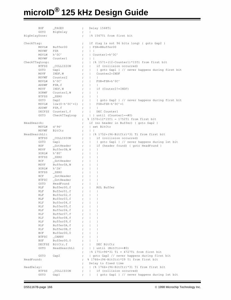
microID® 125 kHz Design Guide
BSF _PAGE0 ; Delay 1568Ti GOTO BigDelay ; |BigDelayDone: ; |% 1567Ti from first bit
CheckTtag: ; if (tag is not 96 bits long) goto Gap2 MOVLW Buffer00 ; | FSR=#Buffer00 MOVWF FSR ; | | MOVLW h’0C’ ; | Counter1=h’0C’ MOVWF Counter1 ; | |CheckTTagLoop: ; | % 1571+(12-Counter1)*15Ti from first bit BTFSS _COLLISION ; | if (collision occurred) GOTO Gap1 ; | goto Gap1 // never happens during first bit MOVF INDF,W ; | Counter2=INDF MOVWF Counter2 ; | | MOVLW h’0C’ ; | FSR=FSR+h’0C’ ADDWF FSR,f ; | | MOVF INDF,W ; | if (Couter2!=INDF) XORWF Counter2,W ; | | BTFSS _ZERO ; | | GOTO Gap2 ; | goto Gap2 // never happens during first bit MOVLW low(0-h’0C’+1) ; | FSR=FSR-h’0C’+1 ADDWF FSR,f ; | | DECFSZ Counter1,f ; | DEC Counter1 GOTO CheckTTagLoop ; | until (Counter1==#0) ; % 1570+12*15Ti = 1752Ti from first bitHeadSearch: ; if (no header in Buffer) goto Gap2 MOVLW d’96’ ; | set BitCtr MOVWF BitCtr ; | |HeadSearchL1: ; | % 1752+(96-BitCtr)*31 Ti from first bit BTFSS _COLLISION ; | if (collision occurred) GOTO Gap1 ; | goto Gap1 // never happens during 1st bit BSF _GotHeader ; | if (header found) goto HeadFound MOVF Buffer0B,W ; | | XORLW h’80’ ; | | BTFSS _ZERO ; | | BCF _GotHeader ; | | MOVF Buffer0A,W ; | | XORLW h’2A’ ; | | BTFSS _ZERO ; | | BCF _GotHeader ; | | BTFSC _GotHeader ; | | GOTO HeadFound ; | | RLF Buffer00,f ; | ROL Buffer RLF Buffer01,f ; | | RLF Buffer02,f ; | | RLF Buffer03,f ; | | RLF Buffer04,f ; | | RLF Buffer05,f ; | | RLF Buffer06,f ; | | RLF Buffer07,f ; | | RLF Buffer08,f ; | | RLF Buffer09,f ; | | RLF Buffer0A,f ; | | RLF Buffer0B,f ; | | BCF Buffer00,0 ; | | BTFSC _CARRY ; | | BSF Buffer00,0 ; | | DECFSZ BitCtr,f ; | DEC BitCtr GOTO HeadSearchL1 ; | until (BitCtr==#0) ; |% 1751+96*31 Ti = 4727Ti from first bit GOTO Gap2 ; | goto Gap2 // never happens during first bitHeadFound: ; % 1766+(96-BitCtr)*29 Ti from first bit ; Delay to fixed timeHeadDelay: ; | % 1766+(96-BitCtr)*31 Ti from first bit BTFSS _COLLISION ; | if (collision occurred) GOTO Gap1 ; | goto Gap1 // never happens during 1st bit
DS51167B-page 166 1998 Microchip Technology Inc.

FSK Anti-Collision Reader Reference Design
CALL Delay08 ; | Delay 26Ti CALL Delay08 ; | | CALL Delay06 ; | | CALL Delay04 ; | | DECFSZ BitCtr,f ; | DEC BitCtr GOTO HeadDelay ; | until (BitCtr==#0) ; % 1765+96*31 = 4741Ti from first bit
BTFSS _COLLISION ; if (collision occurred) GOTO Gap1 ; goto Gap1 // never happens during 1st bit
; % 4743Ti from first bit
BSF _LED2 ; LEDs “Found tag” CALL Delay08 ; | BCF _LED1 ; | ; % 4753Ti from first bit
SWAPF Buffer0B,W ; Transmit tag ID CALL RS232TxDigit ; |%% CALL RS232TxDigit takes 1057Ti MOVF Buffer0B,W ; | CALL RS232TxDigit ; |%% CALL RS232TxDigit takes 1057Ti SWAPF Buffer0A,W ; | CALL RS232TxDigit ; |%% CALL RS232TxDigit takes 1057Ti MOVF Buffer0A,W ; | CALL RS232TxDigit ; |%% CALL RS232TxDigit takes 1057Ti SWAPF Buffer09,W ; | CALL RS232TxDigit ; |%% CALL RS232TxDigit takes 1057Ti MOVF Buffer09,W ; | CALL RS232TxDigit ; |%% CALL RS232TxDigit takes 1057Ti SWAPF Buffer08,W ; | CALL RS232TxDigit ; |%% CALL RS232TxDigit takes 1057Ti MOVF Buffer08,W ; | CALL RS232TxDigit ; |%% CALL RS232TxDigit takes 1057Ti SWAPF Buffer07,W ; | CALL RS232TxDigit ; |%% CALL RS232TxDigit takes 1057Ti MOVF Buffer07,W ; | CALL RS232TxDigit ; |%% CALL RS232TxDigit takes 1057Ti SWAPF Buffer06,W ; | CALL RS232TxDigit ; |%% CALL RS232TxDigit takes 1057Ti MOVF Buffer06,W ; | CALL RS232TxDigit ; |%% CALL RS232TxDigit takes 1057Ti SWAPF Buffer05,W ; | CALL RS232TxDigit ; |%% CALL RS232TxDigit takes 1057Ti MOVF Buffer05,W ; | CALL RS232TxDigit ; |%% CALL RS232TxDigit takes 1057Ti SWAPF Buffer04,W ; | CALL RS232TxDigit ; |%% CALL RS232TxDigit takes 1057Ti MOVF Buffer04,W ; | CALL RS232TxDigit ; |%% CALL RS232TxDigit takes 1057Ti SWAPF Buffer03,W ; | CALL RS232TxDigit ; |%% CALL RS232TxDigit takes 1057Ti MOVF Buffer03,W ; | CALL RS232TxDigit ; |%% CALL RS232TxDigit takes 1057Ti SWAPF Buffer02,W ; | CALL RS232TxDigit ; |%% CALL RS232TxDigit takes 1057Ti MOVF Buffer02,W ; | CALL RS232TxDigit ; |%% CALL RS232TxDigit takes 1057Ti SWAPF Buffer01,W ; | CALL RS232TxDigit ; |%% CALL RS232TxDigit takes 1057Ti MOVF Buffer01,W ; | CALL RS232TxDigit ; |%% CALL RS232TxDigit takes 1057Ti SWAPF Buffer00,W ; | CALL RS232TxDigit ; |%% CALL RS232TxDigit takes 1057Ti MOVF Buffer00,W ; |
1998 Microchip Technology Inc. DS51167B-page 167

microID® 125 kHz Design Guide
CALL RS232TxDigit ; |%% CALL RS232TxDigit takes 1057Ti;% 30145Ti from first bit
CALL RS232CR ;%% CALL RS232CR takes 1052Ti ;% 31197Ti from first bit
MOVLW d’255’ ; Delay 7396Ti MOVWF DelayReg1 ; |WaitingL1: ; | CLRWDT ; | CALL Delay10 ; | CALL Delay10 ; | CALL Delay05 ; | DECFSZ DelayReg1,f ; | GOTO WaitingL1 ; |
;% 38593Ti from first bit;% 38400+193 = 193Ti from first bit, -7Ti from gap INCFSZ GapCountLo,f ; INC GapCount SKIP ; | INCF GapCountHi,f ; | BTFSC GapCountHi,0 ; until (GapCount>#257) BTFSS GapCountLo,1 ; | GOTO GapLoop ; | GOTO BigLoop1
Gap1: ; !!!!! goto here after collision
; % -4Ti from gap CLRF GapCountHi CLRF GapCountLo GOTO GapLoop
GapX: ;% 76+(Counter1*8)Ti from bitGapXDelay: ; Delay 3+(128-Counter1)*8Ti BTFSC Counter1,7 ; | GOTO GapXDelayDone ; | INCF Counter1,f ; | NOP ; | GOTO GapXDelayJ1 ; |GapXDelayJ1: ; | GOTO GapXDelay ; |GapXDelayDone: ; | ;% 76+(oldCounter1)*8+3+128*8-(oldCounter1)*8Ti from bit ;% 1103Ti from bit = (400*2)+303Ti from bit ;// Not in first half of bitGap0: ; !!!!! goto here for gap which does NOT occur in first half of first bit ; % -7Ti from gap INCFSZ GapCountLo,f ; INC GapCount SKIP ; | INCF GapCountHi,f ; |
BTFSC GapCountHi,0 ; until (GapCount>#257) BTFSS GapCountLo,1 ; | GOTO GapLoop ; | GOTO BigLoop1
Gap2: ; !!!!! goto here for valid FSK but invalid code INCFSZ GapCountLo,f ; INC GapCount SKIP ; | INCF GapCountHi,f ; | BTFSC GapCountHi,0 ; until (GapCount>#257) BTFSS GapCountLo,1 ; | GOTO GapLoop ; | GOTO BigLoop1
DS51167B-page 168 1998 Microchip Technology Inc.

FSK Anti-Collision Reader Reference Design
org h’0200’P1Delay20: GOTO P1Delay18P1Delay18: NOPP1Delay17: NOPP1Delay16: GOTO P1Delay14P1Delay14: NOPP1Delay13: NOPP1Delay12: GOTO P1Delay10P1Delay10: GOTO P1Delay08P1Delay08: GOTO P1Delay06P1Delay06: GOTO P1Delay04P1Delay04: RETLW 0
BigDelay:;!!!!! delay (1568-6)Ti = 1562Ti
MOVLW d’15’ ; Delay 1501Ti MOVWF DelayReg1 ; |BigDelayL1: ; | CALL P1Delay20 ; | CALL P1Delay20 ; | CALL P1Delay20 ; | CALL P1Delay20 ; | CALL P1Delay17 ; | DECFSZ DelayReg1,f ; | GOTO BigDelayL1 ; | CALL P1Delay20 ; Delay 61Ti CALL P1Delay20 ; | CALL P1Delay20 ; | NOP ; |
BCF _PAGE0 GOTO BigDelayDone
P1DelayTtag: ; Delay 38393Ti CLRF DelayReg1 ; | Delay 38144TiP1DelayTtagL1: ; | | CALL P1Delay20 ; | | CALL P1Delay20 ; | | CALL P1Delay20 ; | | CALL P1Delay20 ; | | CALL P1Delay20 ; | | CALL P1Delay20 ; | | CALL P1Delay20 ; | | CALL P1Delay06 ; | | DECFSZ DelayReg1,f ; | | GOTO P1DelayTtagL1 ; | | MOVLW d’19’ ; | Delay 248Ti MOVLW DelayReg1 ; | |P1DelayTtagL2: ; | | CALL P1Delay10 ; | | DECFSZ DelayReg1,f ; | | GOTO P1DelayTtagL2 ; | |
1998 Microchip Technology Inc. DS51167B-page 169

microID® 125 kHz Design Guide
NOP ; | Delay 1Ti BCF _PAGE0 RETLW 0ResetDelay: CALL RS232CR ; Transmit CR regularly MOVLW d’4’ ; Beep at 3597Hz for 1024 cycles MOVWF BeepCtrHi ; | MOVLW d’0’ ; | MOVWF BeepCtrLo ; |% 27277Ti from first bitBeepLoopJ1: ; | GOTO BeepLoopJ2 ; |BeepLoopJ2: ; | MOVLW Beep1 ; | MOVWF BeepPort ; | MOVLW d’34’ ; | Delay 137Ti MOVWF DelayReg1 ; | |BeepD1: ; | | CLRWDT ; | | DECFSZ DelayReg1,f ; | | GOTO BeepD1 ; | | MOVLW Beep2 ; | MOVWF BeepPort ; | MOVLW d’32’ ; | Delay 132Ti MOVWF DelayReg1 ; | | NOP ; | | GOTO BeepD2 ; | |BeepD2: ; | | CLRWDT ; | | DECFSZ DelayReg1,f ; | | GOTO BeepD2 ; | | DECFSZ BeepCtrLo,f ; | GOTO BeepLoopJ1 ; | DECFSZ BeepCtrHi,f ; | GOTO BeepLoopJ2 ; | NOP ; | MOVLW Beep0 ; | MOVWF BeepPort ; |
MOVLW d’20’ ; Wait ~10ms (reset gap) MOVWF Counter1 ; |ResetGapL1: ; | MOVLW d’124’ ; | Wait ~500us MOVWF DelayReg1 ; | |ResetGapL2: ; | | CLRWDT ; | | DECFSZ DelayReg1,f ; | | GOTO ResetGapL2 ; | | DECFSZ Counter1,f ; | GOTO ResetGapL1 ; | BSF _FirstTime
Coil_On ; Turn coil on MOVLW d’6’ ; Wait ~6ms MOVWF Counter1 ; |ResetDelayL1: ; | MOVLW d’250’ ; | MOVWF DelayReg1 ; |ResetDelayL2: ; | CLRWDT ; | DECFSZ DelayReg1,f ; | GOTO ResetDelayL2 ; | DECFSZ Counter1,f ; | GOTO ResetDelayL1 ; | BCF _PAGE0 GOTO ResetDelayDone
end
DS51167B-page 170 1998 Microchip Technology Inc.

MCRF2XXUsing the microID® Programmer
1.0 INTRODUCTION
Microchip’s MCRF2XX family of RFID products isnormally programmed at the factory (SQTP™ – seeTechnical Brief TB023 (DS91023), but can be contact-lessly programmed by hand during system develop-ment using a microID development kit or programmer.A contactless programmer (PG103001), user interfacesoftware (rfLAB™), and a host computer are needed toprogram the MCRF2XX devices. The programmer canalso be controlled by a standard terminal (i.e., c:\win-dows\terminal.exe) in place of rfLAB software, butrfLAB software is recommended. See Figure 5-1 for theprogramming sequence.
The microID programmer requires an external powersupply (+9 VDC, >750 mA). The rfLAB software runsunder Microsoft® (MS) Windows® 95, 98, 2000 and XP.The programmer communicates with a host computervia an RS-232 serial interface at 9600 baud, 8 data bits,1 Stop bit and no parity.
The PG103001 programmer (also included inDV103001 and DV103002 kits) is optimized forprogramming ISO card and clamshell cards, such asthose provided in the DV103001 and DV103002 kits.Other tag sizes and shapes may be programmed aswell, but programming yield in that case is unknown.
Since the MCRF2XX is a One-Time-Programmable(OTP) device, only a blank (unlocked) device can beprogrammed by the programmer. Therefore, theprogrammer first checks the status of the memory inthe device before initiating programming. A blankdevice contains an array of all ‘1’s.
The device can be programmed with 16 bytes (128 bits)or 12 bytes (96 bits) of data length. Once the MCRF2XXenters its Programming mode, it sets a lock bit at thesame time. If the programming is interrupted for anyreason during the programming period, the program-ming will be stopped and the device may be left partiallyprogrammed. The device will still be locked even thoughit has not been programmed completely. In this case, theprogrammer will return a fail code to the host computer.
Any device that has been programmed, either fully orpartially, will remain in a locked status; therefore, itcannot to be reprogrammed. If programming has beensuccessfully completed, the programmer will return averification code to the host computer.
In order to program the MCRF2XX device, it isnecessary to provide a proper programming signallevel to the device. The device requires specific peak-to-peak voltages for programming. Since the voltageinduced in the tag coil varies depending on the coilparameters, the output signal level of the programmermust be calibrated to provide a proper programmingsignal level at the tag coil. A detailed calibrationprocedure is described in Section 3.0 “Calibration ofProgramming Voltage”.
FIGURE 1-1: rfLAB™ SOFTWARE RUNNING UNDER MS WINDOWS 95
2004 Microchip Technology Inc. DS51139C-page 171

microID® 125 kHz Design Guide
2.0 PROGRAMMING SIGNAL WAVEFORM
Figure 2-1 shows the waveform of the programmingsignal. Once the programmer sends a power-up andgap signal to the device, the device transmits back averification bit stream in FSK. The verification signalrepresents the contents of the memory in the device.The blank device has all ‘1’s in its memory. A bit ‘1’ inFSK is represented by a low signal level for five cyclesand a high signal level for an additional five cycles(Figure 2-1).
The device will respond with a nonmodulated (no data)signal if the device has not recognized the power-upsignal. In this case, the power-up signal level should becalibrated to provide a proper signal level to the device.The calibration procedure is explained in Section 3.0“Calibration of Programming Voltage”.
After the device is verified as blank, the programmersends a programming signal to the device. Theprogramming data is represented by an amplitudemodulation signal. Therefore, bit ‘1’ and ‘0’ are repre-sented by a low-power (level) signal and a high-power(level) signal, respectively, as shown in Figure 2-1.Each data bit is represented by 128 cycles of the carriersignal. An microID® 125 kHz Design Guide configuredfor 128 bits uses all bits in the transfer; an microID® 125kHz Design Guide configured for 96 bits ignores bits 33through 64, although they are present in the program-ming sequence. Therefore, for a 125 kHz carrier signal,it takes 1.024 ms for one data bit (128 cycles x 8 µs/cycles) and 131.072 ms for 128 data bits (128 cycles/bit x 8 µs/cycle x 128 bits).
A guardband of ∆t = 10 cycles (80 µs) should be keptat each end of a high power (0) bit as shown inFigure 2-1. This is to prevent accidental programmingor disturbing of adjacent bits in the array.
The memory array is locked at the start of the program-ming cycle. Therefore, when the device leaves theprogramming field, it locks the memory permanently,regardless of the programming status. The deviceshould not be interrupted during the programmingcycle.
The device transmits the programmed (data contents)circuits back to the programmer for verification. If theverification bit stream is correct, the programmer sendsa verified signal (‘v’) to the host computer; otherwise, itsends an error message (‘n’, see Figure 5-1).
The programming signal level must be within a limit of theprogramming voltage window for successfulprogramming. The calibration of the signal level isexplained in Section 3.0 “Calibration of ProgrammingVoltage”.
2.1 Power-up, Gap and Verification Signals
The programming signal starts with a power-up signalfor 80 ~ 180 µS, followed by a gap signal (0 volt) for50 ~ 100 µS. The purpose of these signals is to checkwhether the device is blank and establish a Program-ming mode in the device. Once the device recognizesthe power-up signal, it transmits back the contents ofits memory. If the device transmits back with the blankbit stream (FSK with all ‘1’s), it is ready to be pro-grammed. If the device is not blank, the programmerinforms the host computer that it is nonprogrammable.
If the power-up signal level is out of the programmingvoltage range, the device will transmit back a nonmod-ulated signal (no data). The nonmodulated signal hasno variation in the amplitude (constant voltage signal).A variable resistor, R5 in the microID programmer,should be adjusted to provide a proper power-up signallevel. A typical signal level is about 22 ± 3 VPP acrossthe tag coil. This calibration procedure is described inSection 3.0 “Calibration of Programming Voltage”.
2.2 Programming Sequence
Once the device has been verified blank for program-ming, the programmer sends a programming sequenceto the device. The programming data entered in therfLAB software is sent to the device via theprogrammer. The programming signal waveforms areshown in Figure 2-1. One bit of data is represented by128 cycles of the carrier signal. It takes 131.072 ms tocomplete one programming cycle for the total of 128data bits. An microID® 125 kHz Design Guide config-ured for 128 bits uses all bits in the transfer; anmicroID® 125 kHz Design Guide configured for 96 bitsignores bits 33 through 64, although they are present inthe programming sequence. After the programmingsequence, the device transmits back a verification bitstream. The programmer reports to the host computerthe status of the programming.
The data is programmed only if the programming signallevel is within the limit in the programming voltagerequirement of the device. It takes severalProgramming/Verify cycles to completely programeach bit of the microID® 125 kHz Design Guide. ThemicroID programmer uses ten (10) blind Program/Ver-ify cycles before checking the final verify sequence forcorrect programming. Faster programmers can bedesigned by checking each Program/Verify cycle; afterapproximately 3 ~ 5 cycles, the device will verify cor-rectly. Once a correct verify sequence is received, oneadditional program cycle should be run to ensureproper programming margin.
DS51139C-page 172 2004 Microchip Technology Inc.

MCRF2XX
FIGURE 2-1: CONTACTLESS PROGRAMMING WAVEFORM
PO
WE
R-U
PG
AP
~ 5
0 -
100
µsN
ot M
odul
atin
g Mod
ulat
ing
Hig
h P
ower
30 ±
2 V
PP
Bit
1B
it 2
128
bits
x 1
28 c
ycle
s/bi
t x 8
µs/
cycl
e =
131
.1 m
s 13
.5 ±
1 V
PP
Con
tact
less
Pro
gram
min
g P
roto
col
f = 1
25 k
Hz
t = 8
µs
Bit
3…
PR
OG
RA
M
1 bi
t = 1
28 c
ycle
s x
8 µs
/cyc
le =
1.0
24 m
s
80 -
180
µs
VE
RIF
YF
SK
Sig
nal
(R5)
128
bits
∆t =
Gua
rdba
nd
0V
13.5
± 1
VP
P
(R5)
Low
Pow
erS
igna
lS
igna
l
∆t
(R7)
13.5
± 1
VP
P
No
te:
Low
-pow
er s
igna
l lea
ves
bit =
1H
igh-
pow
er s
igna
l pro
gram
s bi
t = 0
∆t
Def
ault
prog
ram
min
g pr
otoc
ol =
FS
K, F
c/8/
10, 1
28 b
itsF
or 9
6-bi
t pro
gram
min
g, b
its 3
3-64
are
“do
n’t c
are”
, but
all
128-
bit c
ycle
s m
ust b
e in
the
sequ
ence
.
2004 Microchip Technology Inc. DS51139C-page 173

microID® 125 kHz Design Guide
3.0 CALIBRATION OF PROGRAMMING VOLTAGE
If you are using your own tag coil (with resonantcapacitor) with the microID® 125 kHz Design Guide orMCRF250, you may need to calibrate the programmerfor your circuit. Follow this procedure if you are unableto program your tag.
a) Open the programmer, turn R5 and R6 fullcounter-clockwise. Remove the four screws atthe back of the programmer.
b) Set up the programmer and calibration tag asshown in Figure 3-1.
Set Up:
• Connect the +9 VDC power supply to the programmer.
• Connect the RS-232 cable from the external serial port in the programmer box to a COM port in the host.
• Open up the rfLAB software on the host computer. • Place the calibration tag in the center of the tag
area on the programmer. A calibration tag is any tag using microID® 125 kHz Design Guide or MCRF250 silicon and your own coil and capacitor.
c) Run the programming software (rfLAB).
Power-up Signal Level:
d) Click the Blank Check button in the rfLABsoftware.
If the device is blank, a green bar appears in thewindow with a message indicating that it isblank. If the device is not blank or the power-upsignal is out of range, a red bar appears in thewindow with an error message indicating that itis not blank. The variable resistor (R5) in theprogrammer should be adjusted to provide aproper “low-power” voltage level to the tag coil.A typical signal level is about 13.5 ± 1 VPP at thetag coil, but it can vary outside of this range.
R5: Turn clockwise in 1/16-inch increments
Repeat step (d) while adjusting R5. Once the devicehas been verified as a blank, turn it clockwise one moreincrement. Then move to the next step.
Programming Signal Level:
e) Click on the buttons in rfLAB software for theappropriate data type and protocol for your tag.
f) Enter the programming data in the text box. g) Click the Program button. This will send the
programming data to the device. A typical signallevel for programming is 32 ± 2 VPP at the tagcoil, but can vary outside of this range.
h) After the device has been programmed, ittransmits back the programmed data forverification.
i) If the data has been programmed correctly, agreen bar will appear for a few seconds with amessage indicating Programming successful.
j) If the programming has been unsuccessful dueto insufficient programming signal levels, a mes-sage indicating Programming unsuccessful willappear in the rfLAB software (see Figure 1-1). Inthis case, R7 (“High Power”) must be adjusted toprovide a proper programming signal level to thetag coil. Turn R7 clockwise in 1/16-inchincrements, repeating steps (f) through (h) untilprogramming is successful. Then turn R7clockwise one more increment.
k) After programming is completed successfully,keep these R5 and R7 settings for futureprogramming of your tags. Once this calibrationhas been done, remove the calibration tag fromthe programmer and reinstall the four screws.
Note: The microID® 125 kHz Design Guide orMCRF250 lock may be locked even if theprogramming cycle was unsuccessful;therefore, a new microID® 125 kHz DesignGuide sample may be required for eachpass through steps (f) through (h).
DS51139C-page 174 2004 Microchip Technology Inc.

MCRF2XX
FIGURE 3-1: MCRF2XX microID PROGRAMMER AND CALIBRATION TAG COIL ARRANGEMENT FOR PROGRAMMING SIGNAL LEVEL MEASUREMENT
Place your coil inthe center of the redoutlined area.
®
2004 Microchip Technology Inc. DS51139C-page 175

microID® 125 kHz Design Guide
4.0 PROGRAMMING PROCEDURE
a) Set up the programmer and open up the rfLABsoftware on the host computer.
Set Up:
• Connect the +9 VDC power supply to the programmer.
• Connect from the external serial port in the programmer box to a COM port in the host computer using the RS-232 cable.
b) Place the RFID device at the center of theprogrammer.
c) Click Blank Check button if you want to checkwhether the device is blank. This button can alsobe used to verify that the device is assembledproperly.
d) Enter the programming data in the rfLAB soft-ware and select appropriate data type.
e) If several devices are going to be programmedsequentially by any number, click the AutoIncrement button and specify the incrementnumber.
f) Click the Program button. This will send thedata to the device.
g) If the data has been programmed correctly,there will be a green bar with a message indicat-ing Programming successful.
If the programming has been unsuccessful dueto out-of-range in the programming signal level,a message and red bar will show up indicatingProgramming unsuccessful. In this case, theprogramming signal voltage may need to becalibrated for your tag. See the calibrationprocedure for the programming signal level inthe previous section.
h) Repeat step (a) through (g) for other tags.
4.1 Error Conditions
If the host computer does not send programming datato the programmer for more than 3 seconds, theprogrammer will time out and reset. If the programmerdoes not respond to the host computer, there will be anerror message indicating Programmer time out. Ifinvalid programming data is sent to the programmerduring the loading of the program buffer, theprogrammer will return a message indicating Invalid.
4.2 Programming Precautions
Taking these steps will help to ensure proper program-ming and minimize programming fallout.
a) If your workbench is metal, set the programmeron top of a cardboard box, stack of books orother nonconductive material to elevate theprogrammer at least 6" from the metal surface.
b) Because most computer monitors contain anoscillator in the pass band of the programmer,make sure the programmer is at least 18" fromany PC monitor.
c) Keep the 9V power supply at least 18" awayfrom the programmer.
d) Do not disturb a tag during blank check orprogramming cycle; the programmer must beidle when moving a tag onto the programmer orwhen removing a tag.”Note: The device can’t be programmed unless it
is blank.
DS51139C-page 176 2004 Microchip Technology Inc.

MCRF2XX
FIGURE 4-1: PROGRAMMING FLOW CHART USING rfLAB™ SOFTWARE
Click “Programmer” Menu Button in rfLAB Software.Click “COM Port” Menu Button
Select a COM Port Number
Error Message:“Programmer Time-out”
No
Click “Blank Check” Button in rfLAB SoftwareSignal Level (R5) or try a new tag.
Message with a Green Bar:“Blank/Programmable”
Yes
Programming
Type in Programming
Message with a Green Bar: “Programming Successful”
Error Message with a Red Bar: “Programming Unsuccessful”
Adjust Programming Signal Level
Start
Yes
Yes
Check Cable Connection and COM Port
No
Adjust the Programming Power-up
No
(R5 and R7)
Data in rfLAB Software
Programmerpower-up and
connection ok?
Blankand power-up
signal level ok?
Successful?
Stop
Place a blank tag on programmer
Error message with a“Device not Blank”
or“Device not present”
Send Program Data:Click “Program” Button
Start
(Due to not blankor incorrectpower-up
signal level)
2004 Microchip Technology Inc. DS51139C-page 177

microID® 125 kHz Design Guide
5.0 PROGRAMMING IN A STANDARD TERMINAL MODE
In special cases, the device can also be programmedin a standard Terminal mode by executing theterminal.exe program (c:\windows\terminal.exe) orby any customer production software. The programmersetup, signal waveforms and calibration procedure arethe same as programming with the rfLAB software.
The following is a description of how to interface a hostcomputer to Microchip’s contactless programmerwithout the use of rfLAB software. The programmer willcheck for a blank, unlocked MCRF2XX tag beforeinitiating programming. Once programming has beencompleted, the programmer will return a pass or failcode. The programmer communicates at 9600 baud, 8data bits, 1 Stop bit, and no parity.
Figure 5-1 shows the programming flow andcommunication handshakes between host andprogrammer.
5.1 Programmer Wake-up
Sending an ASCII ‘W’ (57h) to the programmer on theRS-232 interface will tell the programmer to wake-upand be prepared to receive commands. Theprogrammer will reply with ASCII ‘R’ (52h) when it isready.
5.2 Blank Check
Sending an ASCII ‘T’ (54h) will signal the programmerto read the part about being contactlessly programmedand check to see if it is blank (all 1’s) and unlocked. Ifthe part is blank and unlocked, the programmer willreply with an ASCII ‘Y’ (59h) to signify programmingshould continue. If the part is not blank or not unlocked,the programmer will reply with an ASCII ‘N’ (4Eh) toindicate an error. It is always necessary to perform ablank check before programming MCRF2XX devices.
5.2.1 SENDING DATA TO THE PROGRAMMER
If the programmer responds with an ASCII ‘Y’,indicating that the part is blank, the PC can beginpassing the 16 bytes of required data to theprogrammer data buffer. An microID® 125 kHz DesignGuide configured for 128 bits uses all 16 bytes of datain the transfer; when programming a 96-bit device,however, bits 33 through 64 are “don’t care” and areignored by the microID® 125 kHz Design Guide. Thedata should be passed in ASCII equivalent hex bytesand the programmer will acknowledge the receipt ofeach byte by echoing back what it has received. Forexample, to program 05 hex data into the first byte, thePC would send ASCII ‘0’ (30h), the programmer wouldecho ‘0’ back. Next, the programmer would send ASCII‘5’ (35h), and the programmer will echo back ‘5’. All ofthe data must be sent in UPPERCASE ASCIIequivalent only. See Figure 5-1 for a typicalprogramming sequence.
5.3 Program and Verify the Device
After 16 bytes of data have been received by theprogrammer, it is ready to begin programming the databuffer into the MCRF2XX. Sending an ASCII ‘V’ (56h)will tell the programmer to program the 16 bytes it hasreceived and verify that the device has programmedproperly. When the device programs properly, theprogrammer replies with ASCII ‘y’ (79h). If the program-ming was not successful, the programmer replies withASCII ‘n’ (6Eh). A successful programming operationshould take about 3 to 4 seconds per device.
5.4 Error Conditions
If the PC does not send a byte to the programmer formore than 3 seconds, the programmer will time out andreset. The entire programming sequence will need tobe repeated, beginning with the programmer wake-upbyte ASCII ‘W’.
If invalid bytes are sent to the programmer during theloading of the program buffer, the programmer willreturn an ASCII ‘I’ (49h). In this case, the entireprogramming sequence must be repeated, beginningwith the programmer wake-up byte ASCII ‘W’.
DS51139C-page 178 2004 Microchip Technology Inc.

MCRF2XX
FIGURE 5-1: TYPICAL SEQUENCE
PC Send ‘W’ to the programmer
Programmer replies with ‘R’ to the PC
STEP1
STEP2PC Send ‘T’ to the programmer
Programmer replies with ‘Y’if the deviceis OK and ‘N’ ifthere is an error
STEP3
PC Send ‘F’ to prog.
Programmer replieswith ‘F’
WAKE-UP
VERIFY BLANK
PASS 16 BYTESOF DATA
PC Send ‘1’ to prog.
Programmer replieswith ‘1’
PC Send ‘E’ to prog.
Programmer replieswith ‘E’
PC Send ‘2’ to prog.
Programmer replieswith ‘2’
PC Send ‘2’ to prog.
Programmer replieswith ‘2’
PC Send ‘E’ to prog.
Programmer replieswith ‘E’
PC Send ‘1’ to prog.
Programmer replieswith ‘1’
PC Send ‘F’ to prog.
Programmer replieswith ‘F’
F
1
E
2
2
E
1
F
Byte 1
Byte 2
Byte 15
Byte 16
STEP4PROGRAM/VERIFY
PC Send ‘V’ to the programmer to initiatea Program/Verify sequence
Programmer replies with ‘y’if the deviceprograms OK and ‘n’ if there is anerror
Note: See the signal waveforms and calibration procedure in Section 2.0 “ProgrammingSignal Waveform” and Section 3.0 “Calibration of Programming Voltage”.
(ID internal Program/Verify)
The following is the programming sequence necessary to wake-up the programmer,check if a MCRF2XX part is blank, unlocked and ready to be programmed, sendF1E2D3C4B5A6978888796A5B4C3D2E1F ASCII data to the programmer, andinstruct the programmer to program and verify the device.
2004 Microchip Technology Inc. DS51139C-page 179

microID® 125 kHz Design Guide
TABLE 5-1: ASCII CHARACTER SET
Most Significant Characters
Hex 0 1 2 3 4 5 6 7
Lea
st S
ign
ific
ant
Ch
arac
ters
0 NUL DLE Space 0 @ P ` p
1 SOH DC1 ! 1 A Q a q
2 STX DC2 " 2 B R b r
3 ETX DC3 # 3 C S c s
4 EOT DC4 $ 4 D T d t
5 ENQ NAK % 5 E U e u
6 ACK SYN & 6 F V f v
7 Bell ETB ' 7 G W g w
8 BS CAN ( 8 H X h x
9 HT EM ) 9 I Y i y
A LF SUB * : J Z j z
B VT ESC + ; K [ k
C FF FS , < L \ l |
D CR GS - = M ] m
E SO RS . > N ^ n ~
F SI US / ? O _ o DEL
DS51139C-page 180 2004 Microchip Technology Inc.

MCRF2XX
6.0 microID® PROGRAMMER SCHEMATIC
+5V
C1
DB
9F
9 8 7 6 5 4 3 2 1
P2
MA
X232
15GND
T2O
UT
T1O
UT
7148
135431
T2IN
T1IN
R2O
UT
R1O
UT
1V
-
V+
R2IN
R1IN
C2-
C2+
C1-
C1+
U7
16
2 6 12 9 11
10
VEE
+5V
C5
.1 u
F
C4
.1 u
F
VIN
V0
LM
7805C
V
G
U9
+5V
C14
100 u
F, 6V
31
2C
12
.1 u
FC
13
20 u
F, 35V
D2
1N
4002
P1
1 2 3
+
PIC16C73
15
16
17
18
1920
21
22
23
24
25
26
27
28
14
13
12
11
10987654321
RC
3/S
CK
/SC
LR
C4/S
DI/S
DA
RC
2/C
CP
IR
C5/S
D0
RC
1/T
1O
SI/C
CP
2
RC
6/T
X/C
KR
C0/T
1O
SO
/T1C
KI
OS
C2/C
LK
OU
TV
SS
VD
DO
SC
1/C
LK
IN
VS
SR
B0/IN
T
RA
5/S
S/A
N4
RA
4/T
OC
KI
RA
3/A
N3/V
RE
F
RA
2/A
N2
RA
1/A
N1
RA
0/A
N0
MC
LR
RB
1
RB
2
RB
3
RB
4
RB
5
RB
6
RB
7
C3
.1 u
F
C6
.1 u
F
U4
.1 u
F
8.0
0 M
Hz
Y1
R3
470
BZ
174H
C00
1 2
R1
R2
3U
1:A
2 3
1
+5V
1 23
U3:A
74H
C86
U2
S1
G1
S2
G2
D1
D1
D2
D2
1 2 3 45678
6
+5V
C15
.1 u
F
SI9
942
4700 p
F500V
C2
L1
308 u
HC
18
560 p
F
+5V
U3:B
4 56
U1:C
89 10
RC
7/R
X/D
T
D1
D1
D2
D2
S1
G1
S2
G2
CW
1 2 3 4
8 7 6 5R
4
47
WR
5C
CW
500
89
10
U3:C
U1:B
4 5
+5V
C16
.1 u
F
SI9
942
U5 D
1
D1
D2
D2
S1
G1
S2
G2
CW
1 2 3 4
8 7 6 5R
6
10
WR
7C
CW
100
+5V
C17
.1 u
F
SI9
942
U6
11
U3:D
12
13
U1:D
11
13
12
U8:A
34072
12 3
- +
- +
C7
22 p
F
R9
470K
U8:B
7
34072
56
+5V
R10
150K R11
47K
R13
2.2
K
R14
100K
C8
470 p
FC
9470 p
F
R8
10K
R12
100K
C11
1000 p
F
D1
1N
4148
270
LE
D1
2004 Microchip Technology Inc. DS51139C-page 181

microID® 125 kHz Design Guide
7.0 microID® PROGRAMMER BILL OF MATERIALS
Item # Qty Part #Reference Designator
Part Description Manufacturer VendorVendor Part #
1 1 ICA-328-S-ST U4 SOCKET, 28 PIN,.300, MACHINED COLLET
SAMTEC
2 1 -SPARE- SP1, LED1, R1, R2
-SPARE- LOCATION DO NOT INSTALL
3 1 PCC220CNCT-ND C7 CAP SMT, 22 pF NPO 0805
PANASONIC
4 2 0805N471J101NT C8, C9 CAP SMT, 470 pF 5% 100V 0805
MALLORY
5 1 CD15FC561JO3 C18 CAP, 560 pF, MICA, DIPPED, 300V, AX (0.234LS)
CORNELL DUBILIER
MOUSER 5982-15-300V560
6 1 ECU-V1H102JCX C11 CAP SMT, 1000 pF 50V NPO CER, 0805
PANASONIC
7 1 CD19FD472JO3 C2 CAP, 4700 pF, MICA, DIPPED, 500V, AX (0.344LS)
CORNELL DUBILIER
MOUSER 5982-19-500V4700
8 9 250R18Z104MV4E-6 C1, C3-C6, C12, C15-C17
CAP SMT, 0.1 µF 20% 50V 0805
JOHANSON NEWARK 50F3674
9 1 ECS-H1ED106R C13 CAP SMT, 10 µF, TANT ELEC, 25V, 7343
PANASONIC DIGIKEY PCT5106CT-ND
10 1 ECE-V0JA101SP C14 CAP SMT, 100 µF, TANT ELEC, 6.3V, (VS-D)
PANASONIC DIGIKEY PCE3058CT-ND
11 1 LL4148 D1 DIODE SMT, 5uA, 100V, 500 mW, FAST SWITCHING, DL-35
DIODES INC DIGIKEY LL4148DITR-ND
12 1 DL4002 D2 DIODE SMT, RECTIFIER, 1N4002, 1A, 100V, DL-41
DIODES INC. DIGIKEY DL4002DITR-ND
13 1 3345P-1-101 R7 RES, POT, 100 OHM 1/2 RD WW ST SL
BOURNS DIGIKEY 3345P-101-ND
14 1 3345P-1-501 R5 RES, POT, 500 OHM 1/2 RD WW ST SL
BOURNS DIGIKEY 3345P-501-ND
15 1 ERJ-6GEYJ100 R6 RES SMT, 10 OHM 1/10W 5% TYPE 0805
PANASONIC P10ACT-ND
16 1 ERJ-6GEYJ470V R4 RES SMT, 47 OHM 1/10W 5% TYPE 0805
PANASONIC DIGIKEY P470ATR-ND
17 1 ERJ-6GEYJ471V R3 RES SMT, 470 OHM 1/10W 5% TYPE 0805
PANASONIC P470ATR-ND
18 1 ERJ-6GEYJ222V R13 RES SMT, 2.2K OHM 1/10W 5% TYPE 0805
PANASONIC P2.2KATR-ND
DS51139C-page 182 2004 Microchip Technology Inc.

MCRF2XX
19 1 ERJ-6GEYJ103V R8 RES SMT, 10K 1/8W 5% TYPE 0805
PANASONIC DIGIKEY P10KATR-ND
20 1 ERJ-6GEYJ473V R11 RES SMT, 47K OHM 1/10W 5% TYPE 0805
PANASONIC DIGIKEY P473ATR-ND
21 2 ERJ-6GEYJ104V R12, R14 RES SMT, 100K OHM 1/10W 5% TYPE 0805
PANASONIC DIGIKEY P100KATR-ND
22 1 ERJ-6GEYJ154V R10 RES SMT, 150K OHM 1/8W 5% 0805
PANASONIC DIGIKEY P150KATR-ND
23 1 ERJ-6GEYJ474V R9 RES SMT, 470K OHM 1/8W 5% 0805
PANASONIC DIGIKEY P470KATR-ND
24 1 MM74HC00M U1 IC, SMT, 74HC00 QUAD 2 IN NAND (SO-14)
FAIRCHILD SEMICONDUCTOR
DIGIKEY MM74HC00M-ND
25 3 NDS9942 U2, U5, U6 IC, SMT, 9942 MOSFET N-CH & P-CH 20V (SO-8)
FAIRCHILD SEMICONDUCTOR
DIGIKEY NDS9942TR-ND
26 1 MM74HC86MX U3 IC, SMT, 74HC86, QUAD XOR GATE (SO-14)
FAIRCHILD SEMICONDUCTOR
DIGIKEY
27 1 PIC16C73A /P U4 IC, PIC16C73A /P, PLASTIC DIP, 28P, 0.300
MICROCHIP
28 1 MAX232ACSE U7 IC, MAX232ACSE DUAL RS-232 TRANSMITTER/RCVR, (SO-16)
MAXIM DIGIKEY MAX232ACSE-ND
29 1 MC34072D U8 IC, DUAL OP AMP, (SO-8)
MOTOROLA
30 1 L7805CV U9 IC, REG, +5V, 1.5A, 10%, TO-220
SGS THOMSON MOUSER 511-L7805CV
31 1 EFO-EC8004A4 Y1 OSC, 8.00 MHz CER RESONATOR W/CAP 3 PIN
PANASONIC DIGIKEY PX800-ND
32 1 MCT0003-000 L1 INDUCTOR, 162 µH CORNEL DUBILIER
33 1 DE9S-FRS P2 CONN, D-SUB 9P RECPT RT ANGLE
SPC TECHNOLOGY
34 1 DJ005B P1 JACK, POWER, 2.5mm DC PC MOUNT
LZR ELECTRONICS
Item # Qty Part #Reference Designator
Part Description Manufacturer VendorVendor Part #
2004 Microchip Technology Inc. DS51139C-page 183

microID® 125 kHz Design Guide
8.0 PROGRAMMER SOURCE CODE FOR PIC16C73
; #=#=#=#=#=#=#=#=#=#=# PROJECT Microchip Programmer Reader #=#=#=#=#=#=#=#=#=#=#; #=#=#=#=#=#=#=#=#=#=# 16C73A module #=#=#=#=#=#=#=#=#=#=#; rfgopr5.asm; PIC16C73A running at 8.5MHz, Ti = 0.47us; Tcy = 16 Ti
; ///////////////////////////////////////////////////////////////////////////; Revision history; ///////////////////////////////////////////////////////////////////////////;; Ver Date Comment;; 1.00 10/24/97 Shannon/Hugh first pass; 1.04 13 Feb 98 ADDED TIMEOUT TO TESTMOD; LISTP=PIC16C73A
INCLUDE “P16C73A.INC”__config b’11111111110010’; Code Protect off, Brown-out detect on, Power-up timer on, WDT off,; HS oscillator
constant StartPORTA = b’000000’ constant StartTRISA = b’010111’
#define _LED1 PORTB,4 #define _LED2 PORTB,5 #define _BUZZ1 PORTB,6 constant StartPORTB = b’00010010’ constant StartTRISB = b’00000100’ constant StartOPTION = b’10001000’ ; Pullups disabled, TMR0 internal, WDT*1
COUNT1EQU0x20 ; COUNT REGISTERDATA0EQU0x21DATA1EQU0x22DATA2EQU0x23DATA3EQU0x24DATA4EQU0x25DATA5EQU0x26DATA6EQU0x27DATA7EQU0x28DATA8EQU0x29DATA9EQU0x2ADATAAEQU0x2BDATABEQU0x2CDATACEQU0x2DDATADEQU0x2EDATAEEQU0x2FDATAFEQU0x30BIT EQU 0x31OVERPROEQU0x32DELAY1EQU0x33
Software License Agreement
The software supplied herewith by Microchip Technology Incorporated (the “Company”) is intended and supplied to you, theCompany’s customer, for use solely and exclusively with products manufactured by the Company.The software is owned by the Company and/or its supplier, and is protected under applicable copyright laws. All rights are reserved.Any use in violation of the foregoing restrictions may subject the user to criminal sanctions under applicable laws, as well as to civilliability for the breach of the terms and conditions of this license.THIS SOFTWARE IS PROVIDED IN AN “AS IS” CONDITION. NO WARRANTIES, WHETHER EXPRESS, IMPLIED OR STATU-TORY, INCLUDING, BUT NOT LIMITED TO, IMPLIED WARRANTIES OF MERCHANTABILITY AND FITNESS FOR A PARTICU-LAR PURPOSE APPLY TO THIS SOFTWARE. THE COMPANY SHALL NOT, IN ANY CIRCUMSTANCES, BE LIABLE FORSPECIAL, INCIDENTAL OR CONSEQUENTIAL DAMAGES, FOR ANY REASON WHATSOEVER.
DS51139C-page 184 2004 Microchip Technology Inc.

MCRF2XX
DELAY2EQU0x34DelayReg?H = h’35’DelayReg?L = h’36’CycleCtr?H = h’37’CycleCtr?L = h’38’TimerHi = h’39’TimerMid = h’3A’TimerLo = h’3B’BitCtr = h’3C’BO3 = h’3D’RxByte = h’3E’TxByte = h’3F’ByteCtr = h’40’NoiseTimeout = h’41’SampTimeout = h’42’CycleCtr2?L = h’43’CycleCtr2?H = h’44’ #define _RAW_DATA PORTA,4 #define _RS232OUT PORTC,6 #define _CARRY STATUS,0 #define _TMR2ON T2CON,2 #define _RS232IN PORTC,7 #define _ZERO STATUS,2 #define _COIL_PWR_0 PORTB,3 ; cycle at 30ms period (1=low power) #define _COIL_EN PORTB,1
SKIP macro BTFSC PORTA,7 endm
; ***** Reset Vector
org h’000’ CLRF STATUS CLRF PCLATH CLRF INTCON GOTO RESET_A
; ***** Interrupt Vector - no interrupts yet
org h’004’ CLRF STATUS CLRF PCLATH GOTO RESET_A
RS232StopBit ;[0] Delay >=208 cycles with _RS232OUT highBSF _RS232OUT ; |MOVLW d’208’-d’12’+d’40’; |
DelayW12 ;[0] Delay 12+W cyclesMOVWF DelayReg?L ; |
Delay1 ;[0] Delay 11+Delay cyclesMOVLW d’4’ ; |
Delay1L ; |SUBWF DelayReg?L,f ; |BTFSC _CARRY ; |GOTO Delay1L ; |COMF DelayReg?L,W ; |ADDWF PCL,f ; |
Delay07 ;[0] Delay 7 cyclesNOP ; |
Delay06 ;[0] Delay 6 cyclesNOP ; |
Delay05 ;[0] Delay 5 cyclesNOP ; |
Delay04 ;[0] Delay 4 cyclesRETLW h’00’ ; |
2004 Microchip Technology Inc. DS51139C-page 185

microID® 125 kHz Design Guide
RESET_A CLRWDT ; Initialise registers, clear watchdog timer CLRF STATUS ; | Access register page 0 CLRF FSR ; | FSR=#0 MOVLW StartPORTA ; | Initialise PORT registers MOVWF PORTA ; | | MOVLW StartPORTB ; | | MOVWF PORTB ; | | CLRF INTCON ; | Interrupts off MOVLW b’110001’ ; | TMR1 prescale *8, on MOVWF T1CON ; | | MOVLW b’0000000’ ; | TMR2 postscale *1, off, prescale *1 MOVWF T2CON ; | | MOVLW d’8’ ; | Duty on period = 8 Ti @@@ MOVWF CCPR1L ; | | MOVLW b’001100’ ; | CCP1 to PWM, 0,0 extra duty time @@@ MOVWF CCP1CON ; | | MOVLW b’00000000’ ; | A/D convertor OFF MOVWF ADCON0 ; | | BSF STATUS,RP0 ;^| Initialise TRIS registers MOVLW StartTRISA ;^| | MOVWF TRISA ;^| | MOVLW StartTRISB ;^| | MOVWF TRISB ;^| | MOVLW 0x82 MOVWF TRISC MOVLW StartOPTION ;^| Initialise OPTION register MOVWF OPTION_REG ;^| | MOVLW d’15’ ;^| PR2=7 (period of TMR2=16) @@@ MOVWF PR2 ;^| | MOVLW h’03’ ;^| (It says so on page 2-584) MOVWF PCON ;^| | MOVLW b’110’ ;^| No analog inputs MOVWF ADCON1 ;^| | BCF STATUS,RP0 ; | |
; !!!!! set TRIS registers, and other hardware registers. BCF T2CON,2; turn coil off CLRF TMR2 BCF PORTB,3
CALL RS232On
BigLoop1CALL RS232WaitForever
CheckRxByteMOVF RxByte,WXORLW ‘W’BTFSC _ZEROGOTO INTERRUPTCALL RS232OnMOVLW ‘Q’CALL RS232TxWGOTO BigLoop1
INTERRUPTCALL Delay07 ; LED1 on, LED2 on (orange/yellow)BSF _LED1 ; |CALL Delay07 ; |BSF _LED2 ; |CALL Delay07 ; |
INT_WAKEUP MOVLW ‘R’
DS51139C-page 186 2004 Microchip Technology Inc.

MCRF2XX
MOVWF RxByteCALL RS232On ; delayMOVF RxByte,W ; Transmit RxByteCALL RS232TxW ; |CALL RS232Rx ; Read byte from RS-232BTFSC _CARRY ; | (if timeout, goto INT_END)GOTO INT_END ; |MOVF RxByte,W ; if (RxByte<>#’T’)XORLW ‘T’ ; |BTFSS _ZERO ; |GOTO CheckRxByte ; goto CheckRxByte
MOVLW d’10’ MOVWF CycleCtr?H CLRF CycleCtr?L
Top1 BCFPORTB,3; SET FOR LOW VOLTAGECALLDELAY ; CALL A SMALL DELAY
GAP1; THIS IS THE ROUTINE THAT SETS THE GAP
BCF PORTB,3 CALL DELAY
BSF T2CON,2 ; TURN ON THE COIL
MOVLW0x32 ; MOVE 32 HEX TO W, NUMBER CYCLES BEFORE A GAPMOVWFCOUNT1; MOVW W INTO COUNT1
LOOP11DECFSZCOUNT1,1; DECREMENT COUNT 1 UNTIL IT IS ZEROGOTOLOOP11
BCF T2CON,2 ; TURN OFF THE COIL
MOVLW0x40 ; MOVE 10 HEX TO W, DURATION OF GAPMOVWFCOUNT1; MOVW W INTO COUNT1
LOOP21DECFSZCOUNT1,1; DECREMENT COUNT 1 UNTIL IT IS ZEROGOTOLOOP21
BSF T2CON,2 ; TURN THE COIL BACK ON
CALL TWC ; CALL A DELAY FOR AMP TO SETTLE CALL TWC CALL TWC CALL TWC CALL TWC
WaitFall1 ; Wait for falling edgeWaitFall1A ; | Wait for high MOVLW d’200’ ; | | Set timeout MOVWF DelayReg?H ; | | | CLRF DelayReg?L ; | | |WaitFall1AL ; | | DECFSZ DelayReg?L,f ; | | if (timeout) SKIP ; | | | DECFSZ DelayReg?H,f ; | | | SKIP ; | | | GOTO INT_ErrorN ; | | goto INT_ErrorN BTFSS _RAW_DATA ; | | until (_RAW_DATA==#1) GOTO WaitFall1AL ; | | | NOP ; | | | DECFSZ DelayReg?L,f ; | | if (timeout) SKIP ; | | | DECFSZ DelayReg?H,f ; | | |
2004 Microchip Technology Inc. DS51139C-page 187

microID® 125 kHz Design Guide
SKIP ; | | | GOTO INT_ErrorN ; | | goto INT_ErrorN BTFSS _RAW_DATA ; | | until (_RAW_DATA==#1) GOTO WaitFall1AL ; | |WaitFall1B ; | Wait for low MOVLW d’200’ ; | | Set timeout MOVWF DelayReg?H ; | | | CLRF DelayReg?L ; | | |WaitFall1BL ; | | DECFSZ DelayReg?L,f ; | | if (timeout) SKIP ; | | | DECFSZ DelayReg?H,f ; | | | SKIP ; | | | GOTO INT_ErrorN ; | | goto INT_ErrorN BTFSC _RAW_DATA ; | | until (_RAW_DATA==#0) GOTO WaitFall1BL ; | | | NOP ; | | | DECFSZ DelayReg?L,f ; | | if (timeout) SKIP ; | | | DECFSZ DelayReg?H,f ; | | | SKIP ; | | | GOTO INT_ErrorN ; | | goto INT_ErrorN BTFSC _RAW_DATA ; | | until (_RAW_DATA==#0) GOTO WaitFall1BL ; | | |
CLRF DelayReg?L ; Clear timerWaitFall2 ; Time falling edgeWaitFall2A ; | Wait for highWaitFall2AL ; | | NOP ; NOP ; INCF DelayReg?L,f ; | | Increment timer BTFSC DelayReg?L,7 ; | | if timeout, GOTO INT_ErrorN ; | | goto INT_ErrorN BTFSS _RAW_DATA ; | | until (_RAW_DATA==#1) GOTO WaitFall2AL ; | | | NOP ; | | | NOP ; NOP ; INCF DelayReg?L,f ; | | Increment timer BTFSC DelayReg?L,7 ; | | if timeout, GOTO INT_ErrorN ; | | goto INT_ErrorN BTFSS _RAW_DATA ; | | until (_RAW_DATA==#1) GOTO WaitFall2AL ; | | NOP ;WaitFall2B ; | Wait for lowWaitFall2BL ; | | NOP ; NOP ; INCF DelayReg?L,f ; | | Increment timer BTFSC DelayReg?L,7 ; | | if timeout, GOTO INT_ErrorN ; | | goto INT_ErrorN BTFSC _RAW_DATA ; | | until (_RAW_DATA==#0) GOTO WaitFall2BL ; | | | NOP ; | | | NOP ; NOP ; INCF DelayReg?L,f ; | | Increment timer BTFSC DelayReg?L,7 ; | | if timeout, GOTO INT_ErrorN ; | | goto INT_ErrorN BTFSC _RAW_DATA ; | | until (_RAW_DATA==#0) GOTO WaitFall2BL ; | | | ; DelayReg?L*8Ti = period of signal ; period of _RAW_DATA on FSK = Tcy*10 = Ti*160 ; DelayReg?L = 20 if FSK present
DS51139C-page 188 2004 Microchip Technology Inc.

MCRF2XX
; if period does not match FSK, goto INT_ErrorN MOVF DelayReg?L,W ; | if (DelayReg?L<14) ADDLW low(0-d’14’) ; | | BTFSS _CARRY ; | | GOTO INT_ErrorN ; | goto INT_ErrorN ADDLW low(d’14’-d’22’); | if (DelayReg?L>=22) BTFSC _CARRY ; | | GOTO INT_ErrorN ; | goto INT_ErrorN
MOVLW d’7’ ; CycleCtr > 13*128=1664 MOVWF CycleCtr?H ; | MOVLW d’164’ ; | MOVWF CycleCtr?L ; |TestGotLo DECFSZ CycleCtr?L,f SKIP DECFSZ CycleCtr?H,f SKIP GOTO INT_ErrorN MOVLW 0x20 MOVWF COUNT1 BTFSS _RAW_DATA GOTO TestGotHiTestGotLoLoop BTFSS _RAW_DATA GOTO TestGotHi DECFSZ COUNT1,1 GOTO TestGotLoLoop GOTO MChip_Prog
TestGotHi MOVLW 0x20 MOVWF COUNT1 BTFSC _RAW_DATA GOTO TestGotLoTestGotHiLoop BTFSC _RAW_DATA GOTO TestGotLo DECFSZ COUNT1,1 GOTO TestGotHiLoop;END TEST FOR NO MODULATION
MChip_Prog BCF _TMR2ON CALL TWC
CLRF DATA0CLRF DATA1CLRF DATA2CLRF DATA3CLRF DATA4CLRF DATA5CLRF DATA6CLRF DATA7CLRF DATA8CLRF DATA9CLRF DATAACLRF DATABCLRF DATACCLRF DATADCLRF DATAECLRF DATAF
MOVLW ‘Y’ ; RxByte=’Y’MOVWF RxByte ; |
2004 Microchip Technology Inc. DS51139C-page 189

microID® 125 kHz Design Guide
MOVLW DATAF ; FSR=#DATAFMOVWF FSR ; |MOVLW h’20’ ; ByteCtr=#h’20’MOVWF ByteCtr ; |
RS_ByteLoop ; CALL RS232On ; delayMOVF RxByte,W ; Transmit RxByte on RS-232CALL RS232TxW ; |CALL RS232Rx ; Read RS-232 byte into RxByteBTFSC _CARRY ; |(if timeout, goto INT_END)GOTO INT_END ; |MOVF RxByte,W ; BO3=RxByteMOVWF BO3 ; |MOVLW h’30’ ; if (BO3<#h’30’)SUBWF BO3,W ; |BTFSS _CARRY ; |GOTO CheckRxByte ; goto CheckRxByte MOVWF BO3 ; BO3=BO3-#h’30’MOVLW h’3A’-h’30’ ; if (BO3>=#h’3A’-#h’30’)SUBWF BO3,W ; |BTFSS _CARRY ; |GOTO RSDataJ1 ; MOVWF BO3 ; BO3=BO3-#h’3A’+#h’30’MOVLW h’41’-h’3A’ ; if (BO3<#h’41’-#h’3A’)SUBWF BO3,W ; |BTFSS _CARRY ; |GOTO CheckRxByte ; goto CheckRxByte MOVWF BO3 ; BO3=BO3-#h’41’+#h’3A’MOVLW h’47’-h’41’ ; if (BO3>=#h’47’-#h’41’)SUBWF BO3,W ; |BTFSC _CARRY ; |GOTO CheckRxByte ; goto CheckRxByte MOVLW h’0A’ ; BO3=BO3+#h’0A’ADDWF BO3,f ; |
RSDataJ1 ; SWAPF BO3,W ; W = BO3 swapped if ByteCtr,0==#0BTFSC ByteCtr,0 ; | BO3 if ByteCtr,0==#1MOVF BO3,W ; |IORWF INDF,f ; INDF=INDF OR WBTFSC ByteCtr,0 ; if (ByteCtr,0==#1)DECF FSR,f ; FSR=FSR-#1 DECFSZ ByteCtr,f ; DEC ByteCtrGOTO RS_ByteLoop ; until (ByteCtr==#0)
CALL RS232On ; delayMOVF RxByte,W ; Transmit RxByte on RS-232CALL RS232TxW ; |CALL RS232Rx ; Read RS-232 byte into RxByteBTFSC _CARRY ; |( if timeout, goto INT_END)GOTO INT_END ; |MOVF RxByte,W ; if (RxByte!=#’V’)XORLW ‘V’ ; |BTFSS _ZERO ; |GOTO CheckRxByte ; goto CheckRxByte
; ********
Top BCF PORTB,3 ; SET FOR LOW VOLTAGECALLDELAY ; CALL A SMALL DELAY
GAP ; THIS IS THE ROUTINE THAT SETS THE GAP
BCF PORTB,3
DS51139C-page 190 2004 Microchip Technology Inc.

MCRF2XX
CALL DELAY
BSF T2CON,2 ; TURN ON THE COIL
MOVLW0x32 ; MOVE 32 HEX TO W, NUMBER CYCLES BEFORE A GAPMOVWFCOUNT1; MOVW W INTO COUNT1
LOOP1DECFSZCOUNT1,1; DECREMENT COUNT 1 UNTIL IT IS ZEROGOTOLOOP1
BCF T2CON,2 ; TURN OFF THE COIL
MOVLW0x40 ; MOVE 10 HEX TO W, DURATION OF GAPMOVWFCOUNT1; MOVW W INTO COUNT1
LOOP2DECFSZCOUNT1,1; DECREMENT COUNT 1 UNTIL IT IS ZEROGOTOLOOP2
BSF T2CON,2 ; TURN THE COIL BACK ON
MOVLWd’8’; MOVE 5 INTO THE W REGISTERMOVWFOVERPRO; THIS IS THE NUMBER OF OVERPROGRAMMING
CALL TWC ; CALL A DELAY FOR AMP TO SETTLE CALL TWC CALL TWC CALL TWC CALL TWC
MODING CALL TESTMOD CALL PROGRAM
MOVLW 0x60 MOVWF COUNT1BIGDLY CALL TWC ; CALL A DELAY TO ALLOW THE AMP TO SETTLE DECFSZ COUNT1,f GOTO BIGDLY
DECFSZ OVERPRO,1 ; DECREMENT THE OVERPROGRAMMING NUMBERGOTOMODING ; GOTO LOOK FOR THE MODULATION TO STOP
GOTOVERIFY
;***************************************
VERIFY CALL TESTMOD ; Wait for modulation to stop ;% 167Ti of constant _RAW_DATA
StartWatch ; Wait >~Ttag (for mod to start again)
MOVLW h’00’ ; Delay >~262144Ti MOVWF DelayReg?H ; |VerifyD1a ; | MOVLW h’FF’ ; | delay 1021Ti MOVWF DelayReg?L ; | |VerifyD1b ; | | CLRWDT ; | | DECFSZ DelayReg?L,f ; | | GOTO VerifyD1b ; | | DECFSZ DelayReg?H,f ; | GOTO VerifyD1a ; |StopWatch ; |
CLRF BitCtr ; BitCtr=#128 BSF BitCtr,7 ; |
VerifyL1 ;
2004 Microchip Technology Inc. DS51139C-page 191

microID® 125 kHz Design Guide
;% reftime-1345 CLRF CycleCtr?L;% reftime-1344;% reftime-3-10*6-183*7 MOVLW d’10’ ; set NoiseTimeout MOVWF NoiseTimeout ; |;% reftime-1-10*6-183*7;% reftime-1-NTO*6-183*7 MOVLW d’183’ ; set SampTimeout to 80Tcy MOVWF SampTimeout ; |;% reftime+1-NTO*6-183*7;% reftime+1-NTO*6-STO*7
BTFSC _RAW_DATA GOTO VerS1 NOP
VerS0;% reftime+4-NTO*6-STO*7 DECFSZ NoiseTimeout,f SKIP GOTO VerFail BTFSC _RAW_DATA GOTO VerS1VerGot0;% reftime+3-NTO*6-STO*7VerGot0a;% reftime+3-NTO*6-STO*7 CLRWDT DECFSZ SampTimeout,f SKIP GOTO SampleDone BTFSS _RAW_DATA GOTO VerGot0 NOPVerGot0b;% reftime+3-NTO*6-STO*7 CLRWDT DECFSZ SampTimeout,f SKIP GOTO SampleDone BTFSS _RAW_DATA GOTO VerGot0 NOPVerGotRise;% reftime+3-NTO*6-STO*7 CLRWDT DECFSZ SampTimeout,f SKIP GOTO SampleDone INCF CycleCtr?L,f GOTO VerGot1
VerS1;% reftime+4-NTO*6-STO*7 DECFSZ NoiseTimeout,f SKIP GOTO VerFail BTFSS _RAW_DATA GOTO VerS0VerGot1;% reftime+3-NTO*6-STO*7VerGot1a;% reftime+3-NTO*6-STO*7 CLRWDT
DS51139C-page 192 2004 Microchip Technology Inc.

MCRF2XX
DECFSZ SampTimeout,f SKIP GOTO SampleDone BTFSC _RAW_DATA GOTO VerGot1 NOPVerGot1b;% reftime+3-NTO*6-STO*7 CLRWDT DECFSZ SampTimeout,f SKIP GOTO SampleDone BTFSC _RAW_DATA GOTO VerGot1 NOPVerGotFall;% reftime+3-NTO*6-STO*7 CLRWDT DECFSZ SampTimeout,f SKIP GOTO SampleDone INCF CycleCtr?L,f GOTO VerGot0
SampleDone;% reftime+1-NTO*6-STO*7;& STO=0;% reftime+1-NTO*6NoiseMargin;% reftime+1-NTO*6 NOP NOP NOP DECFSZ NoiseTimeout,f GOTO NoiseMargin;% reftime+0-NTO*6;% NTO=0;% reftime+0
BTFSC DATAF,7 GOTO Verify1 NOP
Verify0;% 3 from ref time; if ‘0’ bit, _DATA_IN cycles 10 times in 80 Tcy; CycleCtr?L should be 20 MOVF CycleCtr?L,W ADDLW low(0-d’18’) BTFSS _CARRY GOTO INT_Failure ADDLW low(d’18’-d’22’) BTFSS _CARRY GOTO Bit_Verified GOTO INT_Failure
Verify1;% 3 from ref time; if ‘1’ bit, _DATA_IN cycles 8 times in 80Tcy; CycleCtr?L should be 16 MOVF CycleCtr?L,W ADDLW low(0-d’14’) BTFSS _CARRY GOTO INT_Failure ADDLW low(d’14’-d’18’)
2004 Microchip Technology Inc. DS51139C-page 193

microID® 125 kHz Design Guide
BTFSS _CARRY GOTO Bit_Verified GOTO INT_Failure
Bit_Verified;% 11 from ref time BCF _CARRY BTFSC DATAF,7 BSF _CARRY RLF DATA0,f RLF DATA1,f RLF DATA2,f RLF DATA3,f RLF DATA4,f RLF DATA5,f RLF DATA6,f RLF DATA7,f RLF DATA8,f RLF DATA9,f RLF DATAA,f RLF DATAB,f RLF DATAC,f RLF DATAD,f RLF DATAE,f RLF DATAF,f
;% 30 from ref time
MOVLW d’167’ ; Delay 670Ti MOVWF DelayReg?L ; | NOP ; |VerDelay ; | CLRWDT ; | DECFSZ DelayReg?L,f ; | GOTO VerDelay ; |
;% 700 from ref time;% (ref times 128*16Ti apart = 2048Ti apart);% -1348 from ref time DECFSZ BitCtr,f ; DEC BitCtr GOTO VerifyL1 ; until (BitCtr==#0)
;***************************************
INT_Success CALL RS232On
MOVLW ‘y’CALL RS232TxWGOTO BigLoop1
VerFailINT_Failure
CALL RS232On MOVLW ‘n’ CALL RS232TxW GOTO BigLoop1
INT_END ; RS-232 TIMEOUTNOPGOTO BigLoop1
INT_ErrorNCALL RS232OnMOVLW ‘N’
DS51139C-page 194 2004 Microchip Technology Inc.

MCRF2XX
CALL RS232TxWGOTO BigLoop1
DELAYMOVLW0x05MOVWFDELAY1
HOLD4DECFSZDELAY1,1GOTOHOLD4RETLW0
; TWC lastsTWC MOVLW0xB0 ; WRITE CYCLE TIMER SUBROUTINE
MOVWFDELAY1HOLD1MOVLW0x02
MOVWFDELAY2HOLD2DECFSZDELAY2,1
GOTOHOLD2DECFSZDELAY1,1GOTOHOLD1
RETLW0
BUFFERMOVLW0x58MOVWFDELAY1
HOLD3DECFSZDELAY1,1GOTOHOLD3
NOP NOP RETLW0
TESTMOD; THIS ROUTINE TESTS THE RAW DATA LINE TO SEE IF THE ; PART IS MODULATING OR NOT
; This routine returns when _RAW_DATA stays constant for some time; some time = 7Ti+32*5Ti = 167Ti = 10.4375Tcy
MOVLW d’7’ ; CycleCtr2 > 13*128=1664 MOVWF CycleCtr2?H ; | MOVLW d’164’ ; | MOVWF CycleCtr2?L ; |
TestModLo DECFSZ CycleCtr2?L,f SKIP DECFSZ CycleCtr2?H,f SKIP GOTO INT_Failure MOVLW 0x20 MOVWF COUNT1 BTFSS _RAW_DATA GOTO TestModHiTestModLoLoop BTFSS _RAW_DATA GOTO TestModHi DECFSZ COUNT1,1 GOTO TestModLoLoop RETLW 0TestModHi MOVLW 0x20 MOVWF COUNT1 BTFSC _RAW_DATA GOTO TestModLoTestModHiLoop BTFSC _RAW_DATA GOTO TestModLo DECFSZ COUNT1,1 GOTO TestModHiLoop
2004 Microchip Technology Inc. DS51139C-page 195

microID® 125 kHz Design Guide
;END TEST FOR NO MODULATION RETLW 0
PROGRAM BCFPORTB,3; CLEAR THE HIGH VOLTAGE
MOVLW0x07; MOVW 7 HEX INTO WMOVWFBIT ; MOVE THIS INTO THE BIT COUNTER
WRITEFBTFSSDATAF,7 ; TEST MOST BYTEBSF PORTB,3 ; SET THE HIGH VOLTAGECALLTWC ; CALL THE WRITE CYCLE TIMERBCF STATUS,C ; CLEAR THE CARRY BIT
BTFSC DATAF,7 ; TEST THE MSB BSF STATUS,C ; SET THE CARRY BIT RLF DATAF,1 ; ROTATE DATAF BCFPORTB,3; CLEAR THE HIGH VOLTAGE CALL BUFFER; CALL THE BUFFER TIMER
DECF BIT,1; DECREMENT BIT, SKIP IF ZEROBTFSS BIT,7 ; SKIP IF SET
GOTOWRITEF; GOTO WRITEF IF BIT IS NOT EQUAL TO ZERO NOP NOP NOP NOP NOP NOP NOP
MOVLW0x07; MOVW 7 HEX INTO WMOVWFBIT ; MOVE THIS INTO THE BIT COUNTER
WRITEEBTFSSDATAE,7 ; TEST MOST BYTEBSF PORTB,3 ; SET THE HIGH VOLTAGECALLTWC ; CALL THE WRITE CYCLE TIMERBCF STATUS,C ; CLEAR THE CARRY BIT
BTFSC DATAE,7 ; TEST THE MSB BSF STATUS,C ; SET THE CARRY BIT RLF DATAE,1 ; ROTATE DATAF BCFPORTB,3; CLEAR THE HIGH VOLTAGE CALL BUFFER; CALL THE BUFFER TIMER
DECF BIT,1; DECREMENT BIT, SKIP IF ZEROBTFSS BIT,7 ; SKIP IF SET
GOTOWRITEE; GOTO WRITEE IF BIT IS NOT EQUAL TO ZERO NOP NOP NOP NOP NOP NOP NOP
MOVLW0x07 ; MOVW 7 HEX INTO WMOVWFBIT ; MOVE THIS INTO THE BIT COUNTER
WRITEDBTFSSDATAD,7 ; TEST MOST BYTEBSF PORTB,3 ; SET THE HIGH VOLTAGECALLTWC ; CALL THE WRITE CYCLE TIMERBCF STATUS,C ; CLEAR THE CARRY BIT
BTFSC DATAD,7 ; TEST THE MSB BSF STATUS,C ; SET THE CARRY BIT RLF DATAD,1 ; ROTATE DATAF BCFPORTB,3; CLEAR THE HIGH VOLTAGE CALL BUFFER; CALL THE BUFFER TIMER
DECF BIT,1; DECREMENT BIT, SKIP IF ZEROBTFSS BIT,7 ; SKIP IF SET
GOTOWRITED; GOTO WRITEF IF BIT IS NOT EQUAL TO ZERO NOP NOP
DS51139C-page 196 2004 Microchip Technology Inc.

MCRF2XX
NOP NOP NOP NOP NOP
MOVLW0x07 ; MOVW 7 HEX INTO WMOVWFBIT ; MOVE THIS INTO THE BIT COUNTER
WRITECBTFSSDATAC,7 ; TEST MOST BYTEBSF PORTB,3 ; SET THE HIGH VOLTAGECALLTWC ; CALL THE WRITE CYCLE TIMERBCF STATUS,C ; CLEAR THE CARRY BIT
BTFSC DATAC,7 ; TEST THE MSB BSF STATUS,C ; SET THE CARRY BIT RLF DATAC,1 ; ROTATE DATAF BCFPORTB,3; CLEAR THE HIGH VOLTAGE CALL BUFFER; CALL THE BUFFER TIMER
DECF BIT,1; DECREMENT BIT, SKIP IF ZEROBTFSS BIT,7 ; SKIP IF SET
GOTOWRITEC; GOTO WRITEC IF BIT IS NOT EQUAL TO ZERO NOP NOP NOP NOP NOP NOP NOP
MOVLW0x07 ; MOVW 7 HEX INTO WMOVWFBIT ; MOVE THIS INTO THE BIT COUNTER
WRITEBBTFSSDATAB,7 ; TEST MOST BYTEBSF PORTB,3 ; SET THE HIGH VOLTAGECALLTWC ; CALL THE WRITE CYCLE TIMERBCF STATUS,C ; CLEAR THE CARRY BIT
BTFSC DATAB,7 ; TEST THE MSB BSF STATUS,C ; SET THE CARRY BIT RLF DATAB,1 ; ROTATE DATAF BCFPORTB,3; CLEAR THE HIGH VOLTAGE CALL BUFFER; CALL THE BUFFER TIMER
DECF BIT,1; DECREMENT BIT, SKIP IF ZEROBTFSS BIT,7 ; SKIP IF SET
GOTOWRITEB; GOTO WRITEB IF BIT IS NOT EQUAL TO ZERO NOP NOP NOP NOP NOP NOP NOP
MOVLW0x07 ; MOVW 7 HEX INTO WMOVWFBIT ; MOVE THIS INTO THE BIT COUNTER
WRITEABTFSSDATAA,7 ; TEST MOST BYTEBSF PORTB,3 ; SET THE HIGH VOLTAGECALLTWC ; CALL THE WRITE CYCLE TIMERBCF STATUS,C ; CLEAR THE CARRY BIT
BTFSC DATAA,7 ; TEST THE MSB BSF STATUS,C ; SET THE CARRY BIT RLF DATAA,1 ; ROTATE DATAF BCFPORTB,3; CLEAR THE HIGH VOLTAGE CALL BUFFER; CALL THE BUFFER TIMER
DECF BIT,1; DECREMENT BIT, SKIP IF ZEROBTFSS BIT,7 ; SKIP IF SET
GOTOWRITEA; GOTO WRITEA IF BIT IS NOT EQUAL TO ZERO NOP
2004 Microchip Technology Inc. DS51139C-page 197

microID® 125 kHz Design Guide
NOP NOP NOP NOP NOP NOP
MOVLW0x07 ; MOVW 7 HEX INTO WMOVWFBIT ; MOVE THIS INTO THE BIT COUNTER
WRITE9BTFSSDATA9,7 ; TEST MOST BYTEBSF PORTB,3 ; SET THE HIGH VOLTAGECALLTWC ; CALL THE WRITE CYCLE TIMERBCF STATUS,C ; CLEAR THE CARRY BIT
BTFSC DATA9,7 ; TEST THE MSB BSF STATUS,C ; SET THE CARRY BIT RLF DATA9,1 ; ROTATE DATAF BCFPORTB,3; CLEAR THE HIGH VOLTAGE CALL BUFFER; CALL THE BUFFER TIMER
DECF BIT,1; DECREMENT BIT, SKIP IF ZEROBTFSS BIT,7 ; SKIP IF SET
GOTOWRITE9; GOTO WRITE9 IF BIT IS NOT EQUAL TO ZERO NOP NOP NOP NOP NOP NOP NOP
MOVLW0x07 ; MOVW 7 HEX INTO WMOVWFBIT ; MOVE THIS INTO THE BIT COUNTER
WRITE8BTFSSDATA8,7 ; TEST MOST BYTEBSF PORTB,3 ; SET THE HIGH VOLTAGECALLTWC ; CALL THE WRITE CYCLE TIMERBCF STATUS,C ; CLEAR THE CARRY BIT
BTFSC DATA8,7 ; TEST THE MSB BSF STATUS,C ; SET THE CARRY BIT RLF DATA8,1 ; ROTATE DATAF BCFPORTB,3; CLEAR THE HIGH VOLTAGE CALL BUFFER; CALL THE BUFFER TIMER
DECF BIT,1; DECREMENT BIT, SKIP IF ZEROBTFSS BIT,7 ; SKIP IF SET
GOTOWRITE8; GOTO WRITE8 IF BIT IS NOT EQUAL TO ZERO NOP NOP NOP NOP NOP NOP NOP
MOVLW0x07; MOVW 7 HEX INTO WMOVWFBIT ; MOVE THIS INTO THE BIT COUNTER
WRITE7BTFSSDATA7,7 ; TEST MOST BYTEBSF PORTB,3 ; SET THE HIGH VOLTAGECALLTWC ; CALL THE WRITE CYCLE TIMERBCF STATUS,C ; CLEAR THE CARRY BIT
BTFSC DATA7,7 ; TEST THE MSB BSF STATUS,C ; SET THE CARRY BIT RLF DATA7,1 ; ROTATE DATAF BCFPORTB,3; CLEAR THE HIGH VOLTAGE CALL BUFFER; CALL THE BUFFER TIMER
DECF BIT,1; DECREMENT BIT, SKIP IF ZEROBTFSS BIT,7 ; SKIP IF SET
GOTOWRITE7; GOTO WRITE7 IF BIT IS NOT EQUAL TO ZERO
DS51139C-page 198 2004 Microchip Technology Inc.

MCRF2XX
NOP NOP NOP NOP NOP NOP NOP
MOVLW0x07 ; MOVW 7 HEX INTO WMOVWFBIT ; MOVE THIS INTO THE BIT COUNTER
WRITE6BTFSSDATA6,7 ; TEST MOST BYTEBSF PORTB,3 ; SET THE HIGH VOLTAGECALLTWC ; CALL THE WRITE CYCLE TIMERBCF STATUS,C ; CLEAR THE CARRY BIT
BTFSC DATA6,7 ; TEST THE MSB BSF STATUS,C ; SET THE CARRY BIT RLF DATA6,1 ; ROTATE DATAF BCFPORTB,3; CLEAR THE HIGH VOLTAGE CALL BUFFER; CALL THE BUFFER TIMER
DECF BIT,1; DECREMENT BIT, SKIP IF ZEROBTFSS BIT,7 ; SKIP IF SET
GOTOWRITE6; GOTO WRITE6 IF BIT IS NOT EQUAL TO ZERO NOP NOP NOP NOP NOP NOP NOP
MOVLW0x07 ; MOVW 7 HEX INTO WMOVWFBIT ; MOVE THIS INTO THE BIT COUNTER
WRITE5BTFSSDATA5,7 ; TEST MOST BYTEBSF PORTB,3 ; SET THE HIGH VOLTAGECALLTWC ; CALL THE WRITE CYCLE TIMERBCF STATUS,C ; CLEAR THE CARRY BIT
BTFSC DATA5,7 ; TEST THE MSB BSF STATUS,C ; SET THE CARRY BIT RLF DATA5,1 ; ROTATE DATAF BCFPORTB,3; CLEAR THE HIGH VOLTAGE CALL BUFFER; CALL THE BUFFER TIMER
DECF BIT,1; DECREMENT BIT, SKIP IF ZEROBTFSS BIT,7 ; SKIP IF SET
GOTOWRITE5; GOTO WRITE5 IF BIT IS NOT EQUAL TO ZERO NOP NOP NOP NOP NOP NOP NOP
MOVLW0x07 ; MOVW 7 HEX INTO WMOVWFBIT ; MOVE THIS INTO THE BIT COUNTER
WRITE4BTFSSDATA4,7 ; TEST MOST BYTEBSF PORTB,3 ; SET THE HIGH VOLTAGECALLTWC ; CALL THE WRITE CYCLE TIMERBCF STATUS,C ; CLEAR THE CARRY BIT
BTFSC DATA4,7 ; TEST THE MSB BSF STATUS,C ; SET THE CARRY BIT RLF DATA4,1 ; ROTATE DATAF BCFPORTB,3; CLEAR THE HIGH VOLTAGE CALL BUFFER; CALL THE BUFFER TIMER
DECF BIT,1; DECREMENT BIT, SKIP IF ZEROBTFSS BIT,7 ; SKIP IF SET
2004 Microchip Technology Inc. DS51139C-page 199

microID® 125 kHz Design Guide
GOTOWRITE4; GOTO WRITE4 IF BIT IS NOT EQUAL TO ZERO NOP NOP NOP NOP NOP NOP NOP
MOVLW0x07 ; MOVW 7 HEX INTO WMOVWFBIT ; MOVE THIS INTO THE BIT COUNTER
WRITE3BTFSSDATA3,7 ; TEST MOST BYTEBSF PORTB,3 ; SET THE HIGH VOLTAGECALLTWC ; CALL THE WRITE CYCLE TIMERBCF STATUS,C ; CLEAR THE CARRY BIT
BTFSC DATA3,7 ; TEST THE MSB BSF STATUS,C ; SET THE CARRY BIT RLF DATA3,1 ; ROTATE DATAF BCFPORTB,3; CLEAR THE HIGH VOLTAGE CALL BUFFER; CALL THE BUFFER TIMER
DECF BIT,1; DECREMENT BIT, SKIP IF ZEROBTFSS BIT,7 ; SKIP IF SET
GOTOWRITE3; GOTO WRITE3 IF BIT IS NOT EQUAL TO ZERO NOP NOP NOP NOP NOP NOP NOP
MOVLW0x07 ; MOVW 7 HEX INTO WMOVWFBIT ; MOVE THIS INTO THE BIT COUNTER
WRITE2BTFSSDATA2,7 ; TEST MOST BYTEBSF PORTB,3 ; SET THE HIGH VOLTAGECALLTWC ; CALL THE WRITE CYCLE TIMERBCF STATUS,C ; CLEAR THE CARRY BIT
BTFSC DATA2,7 ; TEST THE MSB BSF STATUS,C ; SET THE CARRY BIT RLF DATA2,1 ; ROTATE DATAF BCFPORTB,3; CLEAR THE HIGH VOLTAGE CALL BUFFER; CALL THE BUFFER TIMER
DECF BIT,1; DECREMENT BIT, SKIP IF ZEROBTFSS BIT,7 ; SKIP IF SET
GOTOWRITE2; GOTO WRITE2 IF BIT IS NOT EQUAL TO ZERO NOP NOP NOP NOP NOP NOP NOP
MOVLW0x07 ; MOVW 7 HEX INTO WMOVWFBIT ; MOVE THIS INTO THE BIT COUNTER
WRITE1BTFSSDATA1,7 ; TEST MOST BYTEBSF PORTB,3 ; SET THE HIGH VOLTAGECALLTWC ; CALL THE WRITE CYCLE TIMERBCF STATUS,C ; CLEAR THE CARRY BIT
BTFSC DATA1,7 ; TEST THE MSB BSF STATUS,C ; SET THE CARRY BIT RLF DATA1,1 ; ROTATE DATAF BCFPORTB,3; CLEAR THE HIGH VOLTAGE CALL BUFFER; CALL THE BUFFER TIMER
DECF BIT,1; DECREMENT BIT, SKIP IF ZERO
DS51139C-page 200 2004 Microchip Technology Inc.
MCRF2XX
BTFSS BIT,7 ; SKIP IF SET GOTOWRITE1; GOTO WRITEF IF BIT IS NOT EQUAL TO ZERO NOP NOP NOP NOP NOP NOP NOP
MOVLW0x07 ; MOVW 7 HEX INTO WMOVWFBIT ; MOVE THIS INTO THE BIT COUNTER
WRITE0BTFSSDATA0,7 ; TEST MOST BYTEBSF PORTB,3 ; SET THE HIGH VOLTAGECALLTWC ; CALL THE WRITE CYCLE TIMERBCF STATUS,C ; CLEAR THE CARRY BIT
BTFSC DATA0,7 ; TEST THE MSB BSF STATUS,C ; SET THE CARRY BIT RLF DATA0,1 ; ROTATE DATAF BCFPORTB,3; CLEAR THE HIGH VOLTAGE CALL BUFFER; CALL THE BUFFER TIMER
DECF BIT,1; DECREMENT BIT, SKIP IF ZEROBTFSS BIT,7 ; SKIP IF SET
GOTOWRITE0; GOTO WRITE0 IF BIT IS NOT EQUAL TO ZERO RETLW 0
Delay12 NOPDelay11 GOTO Delay09Delay09 GOTO Delay07
RS232On ;[1] Initialise RS-232BCF _TMR2ON ; | Turn coil offCALL RS232StopBit ; | Transmit stop bitsCALL RS232StopBit ; | |CALL RS232StopBit ; | |CALL RS232StopBit ; | |CALL RS232StopBit ; | |CALL RS232StopBit ; | |CALL RS232StopBit ; | |CALL RS232StopBit ; | |CALL RS232StopBit ; | |CALL RS232StopBit ; | |RETLW h’00’ ; | return
RS232WaitForever ;[1] ~9600 baudBigWaitL1 ; |
CLRWDT ;!|BTFSS _RS232IN ; | if (_RS232IN==#0)GOTO RS232RxL1Done ; | goto RS232RxL1Done NOP ;!|GOTO BigWaitL1 ; | until (0)
RS232Rx ;[1] ~9600 baudMOVLW d’16’ ; | Set timeout of ~2.9sMOVWF TimerHi ; | |CLRF TimerMid ; | |CLRF TimerLo ; | |
RS232RxL1 ; | CLRWDT ;!|BTFSS _RS232IN ; | if (_RS232IN==#0)GOTO RS232RxL1Done ; | goto RS232RxL1Done DECFSZ TimerLo,f ; |
2004 Microchip Technology Inc. DS51139C-page 201

microID® 125 kHz Design Guide
GOTO RS232RxL1 ; | |DECFSZ TimerMid,f ; | |GOTO RS232RxL1 ; | |DECFSZ TimerHi,f ; | |GOTO RS232RxL1 ; | |BSF _CARRY ; | return with errorRETLW h’00’ ; | |
; |RS232RxL1Done ; |% 3 to (+6, +8, +10) - say 10us
; |% 10-104=-94MOVLW d’90’ ;!|CALL DelayW12 ;!|% 9CLRF BitCtr ; | BitCtr=#8BSF BitCtr,3 ; | |
RS232RxLoop ; | % 11MOVLW d’181’ ;!|CALL DelayW12 ;!| % 205CLRF BO3 ; | BO3,1=_RS232INBTFSC _RS232IN ; | |INCF BO3,f ; | |% 208BTFSC _RS232IN ; | |% 1INCF BO3,f ; | |BTFSC _RS232IN ; | |INCF BO3,f ; | |% 4RRF RxByte,f ; | RR RxByteBCF RxByte,7 ; | RxByte,7=BO3,1BTFSC BO3,1 ; | |BSF RxByte,7 ; | |% 8DECFSZ BitCtr,f ; | DEC BitCtrGOTO RS232RxLoop ; | until (BitCtr==#0)BCF _CARRY ; | return with no errorRETLW h’00’ ; | |
RS232TxW ;[1] Transmit W on RS232 at ~9600 baudMOVWF TxByte ; | TxByte=WCALL RS232StopBit ; | stop bitCLRF BitCtr ; | BitCtr=#8BSF BitCtr,3 ; | |BCF _RS232OUT ; | Start bitMOVLW d’191’ ; | |CALL DelayW12 ; | |
RS232TxLoop ; | % 205BTFSS TxByte,0 ; | _RS232OUT=TxByte,0BCF _RS232OUT ; | |% 207BTFSC TxByte,0 ; | |% 208BSF _RS232OUT ; | |% 1RRF TxByte,f ; | RR TxByteMOVLW d’187’ ;!|CALL DelayW12 ;!| % 202DECFSZ BitCtr,f ; | DEC BitCtrGOTO RS232TxLoop ; | until (BitCtr==#0)GOTO RS232TxJ1 ; |
RS232TxJ1 ; |NOP ; |% 207BSF _RS232OUT ; | Stop bitRETLW h’00’ ; | return
end
DS51139C-page 202 2004 Microchip Technology Inc.

2004 Microchip Technology Inc. DS51115F-page 203
microID® 125 kHz Design Guide
NOTES:

DS51115F-page 204 2004 Microchip Technology Inc.
AMERICASCorporate Office2355 West Chandler Blvd.Chandler, AZ 85224-6199Tel: 480-792-7200 Fax: 480-792-7277Technical Support: http://support.microchip.comWeb Address: www.microchip.com
AtlantaAlpharetta, GA Tel: 770-640-0034 Fax: 770-640-0307
BostonWestford, MA Tel: 978-692-3848 Fax: 978-692-3821
ChicagoItasca, IL Tel: 630-285-0071 Fax: 630-285-0075
DallasAddison, TX Tel: 972-818-7423 Fax: 972-818-2924
DetroitFarmington Hills, MI Tel: 248-538-2250Fax: 248-538-2260
KokomoKokomo, IN Tel: 765-864-8360Fax: 765-864-8387
Los AngelesMission Viejo, CA Tel: 949-462-9523 Fax: 949-462-9608
San JoseMountain View, CA Tel: 650-215-1444Fax: 650-961-0286
TorontoMississauga, Ontario, CanadaTel: 905-673-0699 Fax: 905-673-6509
ASIA/PACIFICAustralia - SydneyTel: 61-2-9868-6733 Fax: 61-2-9868-6755
China - BeijingTel: 86-10-8528-2100 Fax: 86-10-8528-2104
China - ChengduTel: 86-28-8676-6200 Fax: 86-28-8676-6599
China - FuzhouTel: 86-591-8750-3506 Fax: 86-591-8750-3521
China - Hong Kong SARTel: 852-2401-1200 Fax: 852-2401-3431
China - ShanghaiTel: 86-21-5407-5533 Fax: 86-21-5407-5066China - ShenyangTel: 86-24-2334-2829Fax: 86-24-2334-2393
China - ShenzhenTel: 86-755-8203-2660 Fax: 86-755-8203-1760
China - ShundeTel: 86-757-2839-5507 Fax: 86-757-2839-5571
China - QingdaoTel: 86-532-502-7355 Fax: 86-532-502-7205
ASIA/PACIFICIndia - BangaloreTel: 91-80-2229-0061 Fax: 91-80-2229-0062
India - New DelhiTel: 91-11-5160-8631Fax: 91-11-5160-8632
Japan - KanagawaTel: 81-45-471- 6166 Fax: 81-45-471-6122
Korea - SeoulTel: 82-2-554-7200 Fax: 82-2-558-5932 or 82-2-558-5934
SingaporeTel: 65-6334-8870 Fax: 65-6334-8850
Taiwan - KaohsiungTel: 886-7-536-4818Fax: 886-7-536-4803
Taiwan - TaipeiTel: 886-2-2500-6610 Fax: 886-2-2508-0102
Taiwan - HsinchuTel: 886-3-572-9526Fax: 886-3-572-6459
EUROPEAustria - WeisTel: 43-7242-2244-399Fax: 43-7242-2244-393Denmark - BallerupTel: 45-4450-2828 Fax: 45-4485-2829
France - MassyTel: 33-1-69-53-63-20 Fax: 33-1-69-30-90-79
Germany - IsmaningTel: 49-89-627-144-0 Fax: 49-89-627-144-44
Italy - Milan Tel: 39-0331-742611 Fax: 39-0331-466781
Netherlands - DrunenTel: 31-416-690399 Fax: 31-416-690340
England - BerkshireTel: 44-118-921-5869Fax: 44-118-921-5820
WORLDWIDE SALES AND SERVICE
10/20/04