MCF5200 ColdFire Family Programmer’s Reference …ieee.uwaterloo.ca/coldfire/5200PRM.pdf ·...
206
MOTOROLA, 1995 μ Motorola reserves the right to make changes without further notice to any products herein. Motorola makes no warranty, representation or guarantee regarding the suitability of its products for any particular purpose, nor does Motorola assume any liability arising out of the application or use of any product or circuit, and specifically disclaims any and all liability, including without limitation consequential or incidental damages. "Typical" parameters can and do vary in different applications. All operating parameters, including "Typicals" must be validated for each customer application by customer's technical experts. Motorola does not convey any license under its patent rights nor the rights of others. Motorola products are not designed, intended, or authorized for use as components in systems intended for surgical implant into the body, or other applications intended to support or sustain life, or for any other application in which the failure of the Motorola product could create a situation where personal injury or death may occur. Should Buyer purchase or use Motorola products for any such unintended or unauthorized application, Buyer shall indemnify and hold Motorola and its officers, employees, subsidiaries, affiliates, and distributors harmless against all claims, costs, damages, and expenses, and reasonable attorney fees arising out of, directly or indirectly, any claim of personal injury or death associated with such unintended or unauthorized use, even if such claim alleges that Motorola was negligent regarding the design or manufacture of the part. Motorola and are registered trademarks of Motorola, Inc. Motorola, Inc. is an Equal Opportunity/Affirmative Action Employer. MCF5200 ColdFire Family Programmer’s Reference Manual TM
Transcript of MCF5200 ColdFire Family Programmer’s Reference …ieee.uwaterloo.ca/coldfire/5200PRM.pdf ·...

MOTOROLA, 1995
µ
Motorola reserves the right to make changes without further notice to any products herein. Motorola makes no warranty, representation or guarantee regarding the suitability of its products for any particular purpose, nor does Motorola assume any liability arising out of the application or use of any product or circuit, and specifically disclaims any and all liability, including without limitation consequential or incidental damages. "Typical" parameters can and do vary in different applications. All operating parameters, including "Typicals" must be validated for each customer application by customer's technical experts. Motorola does not convey any license under its patent rights nor the rights of others. Motorola products are not designed, intended, or authorized for use as components in systems intended for surgical implant into the body, or other applications intended to support or sustain life, or for any other application in which the failure of the Motorola product could create a situation where personal injury or death may occur. Should Buyer purchase or use Motorola products for any such unintended or unauthorized application, Buyer shall indemnify and hold Motorola and its officers, employees, subsidiaries, affiliates, and distributors harmless against all claims, costs, damages, and expenses, and reasonable attorney fees arising out of, directly or indirectly, any claim of personal injury or death associated with such unintended or unauthorized use, even if such claim alleges that Motorola was negligent regarding the design or manufacture of the part. Motorola and are registered trademarks of Motorola, Inc. Motorola, Inc. is an Equal Opportunity/Affirmative Action Employer.
MCF5200
ColdFire Family
Programmer’s
Reference Manual
TM


MOTOROLA
MCF5200 FAMILY PROGRAMMER’S REFERENCE MANUAL
iii
68K FAX-IT
Documentation Comments
FAX 512-891-8593—Documentation Comments Only
The Motorola High-Performance Embedded Systems Technical Communications Depart-ment provides a fax number for you to submit any questions or comments about this docu-ment or how to order other documents. We welcome your suggestions for improving ourdocumentation. Please do not fax technical questions.
Please provide the part number and revision number (located in upper right-hand corner ofthe cover) and the title of the document. When referring to items in the manual, please ref-erence by the page number, paragraph number, figure number, table number, and line num-ber if needed.
When sending a fax, please provide your name, company, fax number, and phone numberincluding area code.
For Internet Access:
Telnet: pirs.aus.sps.mot.com (Login: pirs)WWW: http: / / pirs.aus.sps.mot.com/aesop/hmpg.htmlQuery By Email: [email protected](Type ‘‘HELP’’ in text body.)
For Dial-Up:
Phone: +1-512-891-3650Phone (US or Canada): 1-800-843-3451Connection Settings: N/8/1/FData Rate: < 14,400 bpsTerminal Emulation: VT100Login: pirs
For AESOP Questions:
FAX: +1-512-891-8775EMAIL: [email protected]
For Hotline Questions:
FAX (US or Canada): 1-800-248-8567EMAIL: [email protected]

iv
MCF5200 FAMILY PROGRAMMER’S REFERENCE MANUAL
MOTOROLA
Applications and Technical Information
For questions or comments pertaining to technical information, questions, and applications,please contact one of the following sales offices nearest you.
— Sales Offices —
Field Applications Engineering Available Through All Sales Offices
UNITED STATES
ALABAMA
, Huntsville (205) 464-6800
ARIZONA
, Tempe (602) 897-5056
CALIFORNIA
, Agoura Hills (818) 706-1929
CALIFORNIA
, Los Angeles (310) 417-8848
CALIFORNIA
, Irvine (714) 753-7360
CALIFORNIA
, Rosevllle (916) 922-7152
CALIFORNIA
, San Diego (619) 541-2163
CALIFORNIA
, Sunnyvale (408) 749-0510
COLORADO
, Colorado Springs (719) 599-7497
COLORADO
, Denver (303) 337-3434
CONNECTICUT
, Wallingford (203) 949-4100
FLORIDA
, Maitland (407) 628-2636
FLORIDA
, Pompano Beach/ Fort Lauderdale (305) 486-9776
FLORIDA
, Clearwater (813) 538-7750
GEORGlA
, Atlanta (404) 729-7100
IDAHO
, Boise (208) 323-9413
ILLINOIS
, Chicago/Hoffman Estates (708) 490-9500
INDlANA
, Fort Wayne (219) 436-5818
INDIANA
, Indianapolis (317) 571-0400
INDIANA
, Kokomo (317) 457-6634
IOWA
, Cedar Rapids (319) 373-1328
KANSAS
, Kansas City/Mission (913) 451-8555
MARYLAND
, Columbia (410) 381-1570
MASSACHUSETTS
, Marborough (508) 481-8100
MASSACHUSETTS
, Woburn (617) 932-9700
MICHIGAN
, Detroit (313) 347-6800
MINNESOTA
, Minnetonka (612) 932-1500
MISSOURI
, St. Louis (314) 275-7380
NEW JERSEY
, Fairfield (201) 808-2400
NEW YORK
, Fairport (716) 425-4000
NEW YORK
, Hauppauge (516) 361-7000
NEW YORK
, Poughkeepsie/Fishkill (914) 473-8102
NORTH CAROLINA
, Raleigh (919) 870-4355
OHIO
, Cleveland (216) 349-3100
OHIO
, Columbus/Worthington (614) 431-8492
OHIO
, Dayton (513) 495-6800
OKLAHOMA
, Tulsa (800) 544-9496
OREGON
, Portland (503) 641-3681
PENNSYLVANIA
, Colmar (215) 997-1020 Philadelphia/Horsham (215) 957-4100
TENNESSEE
, Knoxville (615) 584-4841
TEXAS
, Austin (512) 873-2000
TEXAS
, Houston (800) 343-2692
TEXAS
, Plano (214) 516-5100
VIRGINIA
, Richmond (804) 285-2100
WASHINGTON
, Bellevue (206) 454-4160 Seattle Access (206) 622-9960
WISCONSIN
, Milwaukee/Brookfield (414) 792-0122
CANADABRITISH COLUMBIA
, Vancouver (604) 293-7605
ONTARIO
, Toronto (416) 497-8181
ONTARIO
, Ottawa (613) 226-3491
QUEBEC
, Montreal (514) 731-6881
INTERNATIONALAUSTRALIA
, Melbourne (61-3)887-0711
AUSTRALIA
, Sydney (61(2)906-3855
BRAZIL
, Sao Paulo 55(11)815-4200
CHINA
, Beijing 86 505-2180
FINLAND
, Helsinki 358-0-35161191 Car Phone 358(49)211501
FRANCE
, Paris/Vanves 33(1)40 955 900
GERMANY
, Langenhagen/ Hanover 49(511)789911
GERMANY
, Munich 49 89 92103-0
GERMANY
, Nuremberg 49 911 64-3044
GERMANY
, Sindelfingen 49 7031 69 910
GERMANY
, Wiesbaden 49 611 761921
HONG KONG
, Kwai Fong 852-4808333 Tai Po 852-6668333
INDIA
, Bangalore (91-812)627094
ISRAEL
, Tel Aviv 972(3)753-8222
ITALY
, Milan 39(2)82201
JAPAN
, Aizu 81(241)272231
JAPAN
, Atsugi 81(0462)23-0761
JAPAN
, Kumagaya 81(0485)26-2600
JAPAN
, Kyushu 81(092)771-4212
JAPAN
, Mito 81(0292)26-2340
JAPAN
, Nagoya 81(052)232-1621
JAPAN
, Osaka 81(06)305-1801
JAPAN,
Sendai 81(22)268-4333
JAPAN,
Tachikawa 81(0425)23-6700
JAPAN,
Tokyo 81(03)3440-3311
JAPAN
, Yokohama 81(045)472-2751
KOREA
, Pusan 82(51)4635-035
KOREA
, Seoul 82(2)554-5188
MALAYSIA
, Penang 60(4)374514
MEXICO
, Mexico City 52(5)282-2864
MEXICO
, Guadalajara 52(36)21-8977 Marketing 52(36)21-9023 Customer Service 52(36)669-9160
NETHERLANDS
, Best (31)49988 612 11
PUERTO RICO
, San Juan (809)793-2170
SINGAPORE
(65)2945438
SPAIN
, Madrid 34(1)457-8204 or 34(1)457-8254
SWEDEN
, Solna 46(8)734-8800
SWITZERLAND
, Geneva 41(22)7991111
SWITZERLAND
, Zurich 41(1)730 4074
TAlWAN
, Taipei 886(2)717-7089
THAILAND
, Bangkok (66-2)254-4910
UNITED KINGDOM
, Aylesbury 44(296)395-252
FULL LINE REPRESENTATIVESCOLORADO
, Grand Junction Cheryl Lee Whltely (303) 243-9658
KANSAS
, Wichita Melinda Shores/Kelly Greiving (316) 838 0190
NEVADA
, Reno Galena Technology Group (702) 746 0642
NEW MEXICO
, Albuquerque S&S Technologies, lnc. (505) 298-7177
UTAH
, Salt Lake City Utah Component Sales, Inc. (801) 561-5099
WASHINGTON
, Spokane Doug Kenley (509) 924-2322
ARGENTINA
, Buenos Aires Argonics, S.A. (541) 343-1787
HYBRID COMPONENTS RESELLERSElmo Semiconductor (818) 768-7400Minco Technology Labs Inc. (512) 834-2022Semi Dice Inc. (310) 594-4631

MOTOROLA MCF5200 FAMILY PROGRAMMER’S REFERENCE MANUAL v
PREFACE
The MCF5200 ColdFire Family Programmer’s Reference Manual describes the program-ming, capabilities, and operation of the ColdFire Family processors, while the MC68000Family Programmer’s Reference Manual provides instruction details for the EC000 core.
TRADEMARKS
All trademarks reside with their respective owners.

vi MCF5200 FAMILY PROGRAMMER’S REFERENCE MANUAL MOTOROLA

MOTOROLA
MCF5200 FAMILY PROGRAMMER’S REFERENCE MANUAL
vii
TABLE OF CONTENTS
ParagraphNumber
Title PageNumber
Section 1Introduction
1.1 Integer Unit User Programming Model. . . . . . . . . . . . . . . . . . . . . . . . . . 1-1 1.1.1 Data Registers (D7 – D0) . . . . . . . . . . . . . . . . . . . . . . . . . . . . . . . . . . 1-11.1.2 Address Registers (A7 – A0) . . . . . . . . . . . . . . . . . . . . . . . . . . . . . . . . 1-11.1.3 Program Counter (PC). . . . . . . . . . . . . . . . . . . . . . . . . . . . . . . . . . . . . 1-11.1.4 Condition Code Register (CCR) . . . . . . . . . . . . . . . . . . . . . . . . . . . . . 1-21.2 Supervisor Programming Model. . . . . . . . . . . . . . . . . . . . . . . . . . . . . . . 1-31.2.1 Address Register 7 (A7) . . . . . . . . . . . . . . . . . . . . . . . . . . . . . . . . . . . 1-31.2.2 Status Register . . . . . . . . . . . . . . . . . . . . . . . . . . . . . . . . . . . . . . . . . . 1-41.2.3 Vector Base Register (VBR) . . . . . . . . . . . . . . . . . . . . . . . . . . . . . . . . 1-41.3 Integer Data Formats . . . . . . . . . . . . . . . . . . . . . . . . . . . . . . . . . . . . . . . 1-41.4 Organization of Data in Registers . . . . . . . . . . . . . . . . . . . . . . . . . . . . . 1-51.4.1 Organization of Integer Data Formats in Registers . . . . . . . . . . . . . . . 1-51.4.2 Organization of Integer Data Formats in Memory . . . . . . . . . . . . . . . . 1-6
Section 2Addressing Capabilities
2.1 Instruction Format . . . . . . . . . . . . . . . . . . . . . . . . . . . . . . . . . . . . . . . . . 2-12.2 Effective Addressing Modes. . . . . . . . . . . . . . . . . . . . . . . . . . . . . . . . . . 2-22.2.1 Data Register Direct Mode . . . . . . . . . . . . . . . . . . . . . . . . . . . . . . . . . 2-42.2.2 Address Register Direct Mode. . . . . . . . . . . . . . . . . . . . . . . . . . . . . . . 2-42.2.3 Address Register Indirect Mode . . . . . . . . . . . . . . . . . . . . . . . . . . . . . 2-42.2.4 Address Register Indirect with Postincrement Mode. . . . . . . . . . . . . . 2-52.2.5 Address Register Indirect with Predecrement Mode . . . . . . . . . . . . . . 2-62.2.6 Address Register Indirect with Displacement Mode . . . . . . . . . . . . . . 2-72.2.7 Address Register Indirect with Index (8-Bit Displacement) Mode . . . . 2-82.2.8 Program Counter Indirect with Displacement Mode . . . . . . . . . . . . . . 2-92.2.9 Program Counter Indirect with Index (8-Bit Displacement) Mode . . . 2-102.2.10 Absolute Short-Addressing Mode . . . . . . . . . . . . . . . . . . . . . . . . . . . 2-102.2.11 Absolute Long-Addressing Mode . . . . . . . . . . . . . . . . . . . . . . . . . . . 2-102.2.12 Immediate Data . . . . . . . . . . . . . . . . . . . . . . . . . . . . . . . . . . . . . . . . . 2-122.2.13 Effective Addressing Mode Summary . . . . . . . . . . . . . . . . . . . . . . . . 2-122.3 Stack . . . . . . . . . . . . . . . . . . . . . . . . . . . . . . . . . . . . . . . . . . . . . . . . . 2-13
Section 3Instruction Set Summary
3.1 Instruction Summary . . . . . . . . . . . . . . . . . . . . . . . . . . . . . . . . . . . . . . 3-13.1.1 Data Movement Instructions . . . . . . . . . . . . . . . . . . . . . . . . . . . . . . . 3-53.1.2 Integer Arithmetic Instructions . . . . . . . . . . . . . . . . . . . . . . . . . . . . . . 3-63.1.3 Logical Instructions . . . . . . . . . . . . . . . . . . . . . . . . . . . . . . . . . . . . . . 3-83.1.4 Shift Instruction . . . . . . . . . . . . . . . . . . . . . . . . . . . . . . . . . . . . . . . . . 3-8

viii
MCF5200 FAMILY PROGRAMMERS REFERENCE MANUAL
MOTOROLA
TABLE OF CONTENTS
(
Continued
)
ParagraphNumber
Title PageNumber
3.1.5 Bit Manipulation Instructions . . . . . . . . . . . . . . . . . . . . . . . . . . . . . . . 3-93.1.6 Program Control Instructions. . . . . . . . . . . . . . . . . . . . . . . . . . . . . . . 3-93.1.7 System Control Instructions. . . . . . . . . . . . . . . . . . . . . . . . . . . . . . . 3-103.2 Integer Unit Condition Code Computation . . . . . . . . . . . . . . . . . . . . . 3-11
Section 4Integer Instructions
ADD . . . . . . . . . . . . . . . . . . . . . . . . . . . . . . . . . . . . . . . . . . . . . . . . . . . . 4-2ADDA . . . . . . . . . . . . . . . . . . . . . . . . . . . . . . . . . . . . . . . . . . . . . . . . . . . 4-5ADDI. . . . . . . . . . . . . . . . . . . . . . . . . . . . . . . . . . . . . . . . . . . . . . . . . . . . 4-7ADDQ. . . . . . . . . . . . . . . . . . . . . . . . . . . . . . . . . . . . . . . . . . . . . . . . . . . 4-8ADDX . . . . . . . . . . . . . . . . . . . . . . . . . . . . . . . . . . . . . . . . . . . . . . . . . . 4-10AND . . . . . . . . . . . . . . . . . . . . . . . . . . . . . . . . . . . . . . . . . . . . . . . . . . . 4-12ANDI. . . . . . . . . . . . . . . . . . . . . . . . . . . . . . . . . . . . . . . . . . . . . . . . . . . 4-15ASL, ASR . . . . . . . . . . . . . . . . . . . . . . . . . . . . . . . . . . . . . . . . . . . . . . . 4-16Bcc . . . . . . . . . . . . . . . . . . . . . . . . . . . . . . . . . . . . . . . . . . . . . . . . . . . . 4-19BCHG. . . . . . . . . . . . . . . . . . . . . . . . . . . . . . . . . . . . . . . . . . . . . . . . . . 4-21BCLR . . . . . . . . . . . . . . . . . . . . . . . . . . . . . . . . . . . . . . . . . . . . . . . . . . 4-24BRA . . . . . . . . . . . . . . . . . . . . . . . . . . . . . . . . . . . . . . . . . . . . . . . . . . . 4-27BSET . . . . . . . . . . . . . . . . . . . . . . . . . . . . . . . . . . . . . . . . . . . . . . . . . . 4-28BSR . . . . . . . . . . . . . . . . . . . . . . . . . . . . . . . . . . . . . . . . . . . . . . . . . . . 4-31BTST . . . . . . . . . . . . . . . . . . . . . . . . . . . . . . . . . . . . . . . . . . . . . . . . . . 4-33CLR . . . . . . . . . . . . . . . . . . . . . . . . . . . . . . . . . . . . . . . . . . . . . . . . . . . 4-36CMP . . . . . . . . . . . . . . . . . . . . . . . . . . . . . . . . . . . . . . . . . . . . . . . . . . . 4-38CMPA. . . . . . . . . . . . . . . . . . . . . . . . . . . . . . . . . . . . . . . . . . . . . . . . . . 4-40CMPI . . . . . . . . . . . . . . . . . . . . . . . . . . . . . . . . . . . . . . . . . . . . . . . . . . 4-42EOR . . . . . . . . . . . . . . . . . . . . . . . . . . . . . . . . . . . . . . . . . . . . . . . . . . . 4-43EORI. . . . . . . . . . . . . . . . . . . . . . . . . . . . . . . . . . . . . . . . . . . . . . . . . . . 4-45EXT. EXTB. . . . . . . . . . . . . . . . . . . . . . . . . . . . . . . . . . . . . . . . . . . . . . 4-46JMP . . . . . . . . . . . . . . . . . . . . . . . . . . . . . . . . . . . . . . . . . . . . . . . . . . . 4-47JSR. . . . . . . . . . . . . . . . . . . . . . . . . . . . . . . . . . . . . . . . . . . . . . . . . . . . 4-48LEA. . . . . . . . . . . . . . . . . . . . . . . . . . . . . . . . . . . . . . . . . . . . . . . . . . . . 4-49LINK . . . . . . . . . . . . . . . . . . . . . . . . . . . . . . . . . . . . . . . . . . . . . . . . . . . 4-50LSL, LSR . . . . . . . . . . . . . . . . . . . . . . . . . . . . . . . . . . . . . . . . . . . . . . . 4-51MOVE, MOVEA . . . . . . . . . . . . . . . . . . . . . . . . . . . . . . . . . . . . . . . . . . 4-53MOVE from CCR . . . . . . . . . . . . . . . . . . . . . . . . . . . . . . . . . . . . . . . . . 4-56MOVE to CCR . . . . . . . . . . . . . . . . . . . . . . . . . . . . . . . . . . . . . . . . . . . 4-57MOVEM . . . . . . . . . . . . . . . . . . . . . . . . . . . . . . . . . . . . . . . . . . . . . . . . 4-59MOVEQ . . . . . . . . . . . . . . . . . . . . . . . . . . . . . . . . . . . . . . . . . . . . . . . . 4-62MULS . . . . . . . . . . . . . . . . . . . . . . . . . . . . . . . . . . . . . . . . . . . . . . . . . . 4-63MULU . . . . . . . . . . . . . . . . . . . . . . . . . . . . . . . . . . . . . . . . . . . . . . . . . . 4-65

MOTOROLA
MCF5200 FAMILY PROGRAMMERS REFERENCE MANUAL
ix
TABLE OF CONTENTS
(
Continued
)
ParagraphNumber
Title PageNumber
NEG . . . . . . . . . . . . . . . . . . . . . . . . . . . . . . . . . . . . . . . . . . . . . . . . . . . 4-69NEGX . . . . . . . . . . . . . . . . . . . . . . . . . . . . . . . . . . . . . . . . . . . . . . . . . . 4-70NOP . . . . . . . . . . . . . . . . . . . . . . . . . . . . . . . . . . . . . . . . . . . . . . . . . . . 4-72NOT . . . . . . . . . . . . . . . . . . . . . . . . . . . . . . . . . . . . . . . . . . . . . . . . . . . 4-73OR . . . . . . . . . . . . . . . . . . . . . . . . . . . . . . . . . . . . . . . . . . . . . . . . . . . . 4-74ORI . . . . . . . . . . . . . . . . . . . . . . . . . . . . . . . . . . . . . . . . . . . . . . . . . . . . 4-77PEA . . . . . . . . . . . . . . . . . . . . . . . . . . . . . . . . . . . . . . . . . . . . . . . . . . . 4-78RTS . . . . . . . . . . . . . . . . . . . . . . . . . . . . . . . . . . . . . . . . . . . . . . . . . . . 4-79Scc . . . . . . . . . . . . . . . . . . . . . . . . . . . . . . . . . . . . . . . . . . . . . . . . . . . 4-80SUB . . . . . . . . . . . . . . . . . . . . . . . . . . . . . . . . . . . . . . . . . . . . . . . . . . . 4-82SUBA . . . . . . . . . . . . . . . . . . . . . . . . . . . . . . . . . . . . . . . . . . . . . . . . . . 4-85SUBI . . . . . . . . . . . . . . . . . . . . . . . . . . . . . . . . . . . . . . . . . . . . . . . . . . . 4-87SUBQ . . . . . . . . . . . . . . . . . . . . . . . . . . . . . . . . . . . . . . . . . . . . . . . . . . 4-88SUBX . . . . . . . . . . . . . . . . . . . . . . . . . . . . . . . . . . . . . . . . . . . . . . . . . . 4-90SWAP. . . . . . . . . . . . . . . . . . . . . . . . . . . . . . . . . . . . . . . . . . . . . . . . . . 4-92TRAP . . . . . . . . . . . . . . . . . . . . . . . . . . . . . . . . . . . . . . . . . . . . . . . . . . 4-93TRAPF . . . . . . . . . . . . . . . . . . . . . . . . . . . . . . . . . . . . . . . . . . . . . . . . . 4-94TST. . . . . . . . . . . . . . . . . . . . . . . . . . . . . . . . . . . . . . . . . . . . . . . . . . . . 4-95UNLK . . . . . . . . . . . . . . . . . . . . . . . . . . . . . . . . . . . . . . . . . . . . . . . . . . 4-97
Section 5
Supervisor (Privileged) Instructions
HALT . . . . . . . . . . . . . . . . . . . . . . . . . . . . . . . . . . . . . . . . . . . . . . . . . . . 5-3PULSE . . . . . . . . . . . . . . . . . . . . . . . . . . . . . . . . . . . . . . . . . . . . . . . . . . 5-4WDDATA . . . . . . . . . . . . . . . . . . . . . . . . . . . . . . . . . . . . . . . . . . . . . . . . 5-5WDEBUG . . . . . . . . . . . . . . . . . . . . . . . . . . . . . . . . . . . . . . . . . . . . . . . . 5-6MOVE from SR. . . . . . . . . . . . . . . . . . . . . . . . . . . . . . . . . . . . . . . . . . . . 5-7MOVE to SR. . . . . . . . . . . . . . . . . . . . . . . . . . . . . . . . . . . . . . . . . . . . . . 5-8MOVEC . . . . . . . . . . . . . . . . . . . . . . . . . . . . . . . . . . . . . . . . . . . . . . . . 5-10RTE . . . . . . . . . . . . . . . . . . . . . . . . . . . . . . . . . . . . . . . . . . . . . . . . . . . 5-12STOP . . . . . . . . . . . . . . . . . . . . . . . . . . . . . . . . . . . . . . . . . . . . . . . . . . 5-13
Section 6Instruction Format Summary
6.1 Instruction Format . . . . . . . . . . . . . . . . . . . . . . . . . . . . . . . . . . . . . . . . 6-16.1.1 Effective Address Field . . . . . . . . . . . . . . . . . . . . . . . . . . . . . . . . . . . 6-16.1.2 Shift Instruction . . . . . . . . . . . . . . . . . . . . . . . . . . . . . . . . . . . . . . . . . 6-16.1.2.1 Count Register Field . . . . . . . . . . . . . . . . . . . . . . . . . . . . . . . . . . . . 6-16.1.2.2 Register Field . . . . . . . . . . . . . . . . . . . . . . . . . . . . . . . . . . . . . . . . . 6-16.1.3 Size Field . . . . . . . . . . . . . . . . . . . . . . . . . . . . . . . . . . . . . . . . . . . . 6-2
x
MCF5200 FAMILY PROGRAMMERS REFERENCE MANUAL
MOTOROLA
TABLE OF CONTENTS
(
Continued
)
ParagraphNumber
Title PageNumber
6.1.4 Opmode Field . . . . . . . . . . . . . . . . . . . . . . . . . . . . . . . . . . . . . . . . . . 6-26.1.5 Address/Data Field . . . . . . . . . . . . . . . . . . . . . . . . . . . . . . . . . . . . . . 6-26.2 Operation Code Map . . . . . . . . . . . . . . . . . . . . . . . . . . . . . . . . . . . . . . 6-2
ORI . . . . . . . . . . . . . . . . . . . . . . . . . . . . . . . . . . . . . . . . . . . . . . . . . . . . . 6-3ANDI. . . . . . . . . . . . . . . . . . . . . . . . . . . . . . . . . . . . . . . . . . . . . . . . . . . . 6-3SUBI . . . . . . . . . . . . . . . . . . . . . . . . . . . . . . . . . . . . . . . . . . . . . . . . . . . . 6-3ADDI. . . . . . . . . . . . . . . . . . . . . . . . . . . . . . . . . . . . . . . . . . . . . . . . . . . . 6-3EORI. . . . . . . . . . . . . . . . . . . . . . . . . . . . . . . . . . . . . . . . . . . . . . . . . . . . 6-3CMPI . . . . . . . . . . . . . . . . . . . . . . . . . . . . . . . . . . . . . . . . . . . . . . . . . . . 6-3BTST . . . . . . . . . . . . . . . . . . . . . . . . . . . . . . . . . . . . . . . . . . . . . . . . . . . 6-3BCHG. . . . . . . . . . . . . . . . . . . . . . . . . . . . . . . . . . . . . . . . . . . . . . . . . . . 6-4BCLR . . . . . . . . . . . . . . . . . . . . . . . . . . . . . . . . . . . . . . . . . . . . . . . . . . . 6-4BSET . . . . . . . . . . . . . . . . . . . . . . . . . . . . . . . . . . . . . . . . . . . . . . . . . . . 6-4BTST . . . . . . . . . . . . . . . . . . . . . . . . . . . . . . . . . . . . . . . . . . . . . . . . . . . 6-4BCHG. . . . . . . . . . . . . . . . . . . . . . . . . . . . . . . . . . . . . . . . . . . . . . . . . . . 6-4BCLR . . . . . . . . . . . . . . . . . . . . . . . . . . . . . . . . . . . . . . . . . . . . . . . . . . . 6-4BSET . . . . . . . . . . . . . . . . . . . . . . . . . . . . . . . . . . . . . . . . . . . . . . . . . . . 6-4MOVE. . . . . . . . . . . . . . . . . . . . . . . . . . . . . . . . . . . . . . . . . . . . . . . . . . . 6-5MOVE from SR. . . . . . . . . . . . . . . . . . . . . . . . . . . . . . . . . . . . . . . . . . . . 6-5Move from CCR . . . . . . . . . . . . . . . . . . . . . . . . . . . . . . . . . . . . . . . . . . . 6-5NEGX . . . . . . . . . . . . . . . . . . . . . . . . . . . . . . . . . . . . . . . . . . . . . . . . . . . 6-5CLR . . . . . . . . . . . . . . . . . . . . . . . . . . . . . . . . . . . . . . . . . . . . . . . . . . . . 6-5MOVE TO CCR . . . . . . . . . . . . . . . . . . . . . . . . . . . . . . . . . . . . . . . . . . . 6-5MOVE FROM CCR . . . . . . . . . . . . . . . . . . . . . . . . . . . . . . . . . . . . . . . . 6-5NEG . . . . . . . . . . . . . . . . . . . . . . . . . . . . . . . . . . . . . . . . . . . . . . . . . . . . 6-5NOT . . . . . . . . . . . . . . . . . . . . . . . . . . . . . . . . . . . . . . . . . . . . . . . . . . . . 6-5MOVE TO SR. . . . . . . . . . . . . . . . . . . . . . . . . . . . . . . . . . . . . . . . . . . . . 6-6EXT, EXTB. . . . . . . . . . . . . . . . . . . . . . . . . . . . . . . . . . . . . . . . . . . . . . . 6-6SWAP. . . . . . . . . . . . . . . . . . . . . . . . . . . . . . . . . . . . . . . . . . . . . . . . . . . 6-6PEA . . . . . . . . . . . . . . . . . . . . . . . . . . . . . . . . . . . . . . . . . . . . . . . . . . . . 6-6TST. . . . . . . . . . . . . . . . . . . . . . . . . . . . . . . . . . . . . . . . . . . . . . . . . . . . . 6-6HALT . . . . . . . . . . . . . . . . . . . . . . . . . . . . . . . . . . . . . . . . . . . . . . . . . . . 6-6PULSE . . . . . . . . . . . . . . . . . . . . . . . . . . . . . . . . . . . . . . . . . . . . . . . . . . 6-6MULU . . . . . . . . . . . . . . . . . . . . . . . . . . . . . . . . . . . . . . . . . . . . . . . . . . . 6-6MULS . . . . . . . . . . . . . . . . . . . . . . . . . . . . . . . . . . . . . . . . . . . . . . . . . . . 6-7TRAP . . . . . . . . . . . . . . . . . . . . . . . . . . . . . . . . . . . . . . . . . . . . . . . . . . . 6-7LINK . . . . . . . . . . . . . . . . . . . . . . . . . . . . . . . . . . . . . . . . . . . . . . . . . . . . 6-7NOP . . . . . . . . . . . . . . . . . . . . . . . . . . . . . . . . . . . . . . . . . . . . . . . . . . . . 6-7STOP . . . . . . . . . . . . . . . . . . . . . . . . . . . . . . . . . . . . . . . . . . . . . . . . . . . 6-7RTE . . . . . . . . . . . . . . . . . . . . . . . . . . . . . . . . . . . . . . . . . . . . . . . . . . . . 6-7RTS . . . . . . . . . . . . . . . . . . . . . . . . . . . . . . . . . . . . . . . . . . . . . . . . . . . . 6-7MOVEC . . . . . . . . . . . . . . . . . . . . . . . . . . . . . . . . . . . . . . . . . . . . . . . . . 6-8

MOTOROLA
MCF5200 FAMILY PROGRAMMERS REFERENCE MANUAL
xi
TABLE OF CONTENTS
(
Continued
)
ParagraphNumber
Title PageNumber
JSR. . . . . . . . . . . . . . . . . . . . . . . . . . . . . . . . . . . . . . . . . . . . . . . . . . . . . 6-8JMP . . . . . . . . . . . . . . . . . . . . . . . . . . . . . . . . . . . . . . . . . . . . . . . . . . . . 6-8MOVEM . . . . . . . . . . . . . . . . . . . . . . . . . . . . . . . . . . . . . . . . . . . . . . . . . 6-8LEA. . . . . . . . . . . . . . . . . . . . . . . . . . . . . . . . . . . . . . . . . . . . . . . . . . . . . 6-8ADDQ. . . . . . . . . . . . . . . . . . . . . . . . . . . . . . . . . . . . . . . . . . . . . . . . . . . 6-8SUBQ . . . . . . . . . . . . . . . . . . . . . . . . . . . . . . . . . . . . . . . . . . . . . . . . . . . 6-8Scc . . . . . . . . . . . . . . . . . . . . . . . . . . . . . . . . . . . . . . . . . . . . . . . . . . . . . 6-8BRA . . . . . . . . . . . . . . . . . . . . . . . . . . . . . . . . . . . . . . . . . . . . . . . . . . . . 6-8BSR . . . . . . . . . . . . . . . . . . . . . . . . . . . . . . . . . . . . . . . . . . . . . . . . . . . . 6-9Bcc . . . . . . . . . . . . . . . . . . . . . . . . . . . . . . . . . . . . . . . . . . . . . . . . . . . . . 6-9MOVEQ . . . . . . . . . . . . . . . . . . . . . . . . . . . . . . . . . . . . . . . . . . . . . . . . . 6-9OR . . . . . . . . . . . . . . . . . . . . . . . . . . . . . . . . . . . . . . . . . . . . . . . . . . . . . 6-9SUBX . . . . . . . . . . . . . . . . . . . . . . . . . . . . . . . . . . . . . . . . . . . . . . . . . . . 6-9SUB . . . . . . . . . . . . . . . . . . . . . . . . . . . . . . . . . . . . . . . . . . . . . . . . . . . . 6-9SUBA . . . . . . . . . . . . . . . . . . . . . . . . . . . . . . . . . . . . . . . . . . . . . . . . . . . 6-9CMP . . . . . . . . . . . . . . . . . . . . . . . . . . . . . . . . . . . . . . . . . . . . . . . . . . . . 6-9CMPA. . . . . . . . . . . . . . . . . . . . . . . . . . . . . . . . . . . . . . . . . . . . . . . . . . . 6-9EOR . . . . . . . . . . . . . . . . . . . . . . . . . . . . . . . . . . . . . . . . . . . . . . . . . . . 6-10MULU . . . . . . . . . . . . . . . . . . . . . . . . . . . . . . . . . . . . . . . . . . . . . . . . . . 6-10MULS . . . . . . . . . . . . . . . . . . . . . . . . . . . . . . . . . . . . . . . . . . . . . . . . . . 6-10AND . . . . . . . . . . . . . . . . . . . . . . . . . . . . . . . . . . . . . . . . . . . . . . . . . . . 6-10ADDX . . . . . . . . . . . . . . . . . . . . . . . . . . . . . . . . . . . . . . . . . . . . . . . . . . 6-10ADDA . . . . . . . . . . . . . . . . . . . . . . . . . . . . . . . . . . . . . . . . . . . . . . . . . . 6-10ADD . . . . . . . . . . . . . . . . . . . . . . . . . . . . . . . . . . . . . . . . . . . . . . . . . . . 6-10ASL, ASR . . . . . . . . . . . . . . . . . . . . . . . . . . . . . . . . . . . . . . . . . . . . . . . 6-10LSL, LSR . . . . . . . . . . . . . . . . . . . . . . . . . . . . . . . . . . . . . . . . . . . . . . . 6-10WDATA . . . . . . . . . . . . . . . . . . . . . . . . . . . . . . . . . . . . . . . . . . . . . . . . 6-11WDEBUG . . . . . . . . . . . . . . . . . . . . . . . . . . . . . . . . . . . . . . . . . . . . . . . 6-11
Section 7
Exception Processing
7.1 Exception Processing Overview. . . . . . . . . . . . . . . . . . . . . . . . . . . . . . 7-17.2 Exception Stack Frame Definition . . . . . . . . . . . . . . . . . . . . . . . . . . . . 7-57.3 Processor Exceptions. . . . . . . . . . . . . . . . . . . . . . . . . . . . . . . . . . . . . . 7-67.3.1 Access Error Exception . . . . . . . . . . . . . . . . . . . . . . . . . . . . . . . . . . . 7-67.3.2 Address Error Exception . . . . . . . . . . . . . . . . . . . . . . . . . . . . . . . . . . 7-77.3.3 Trap Exception . . . . . . . . . . . . . . . . . . . . . . . . . . . . . . . . . . . . . . . . . 7-77.3.4 Illegal Instruction Exception. . . . . . . . . . . . . . . . . . . . . . . . . . . . . . . . 7-77.3.5 Privilege Violation . . . . . . . . . . . . . . . . . . . . . . . . . . . . . . . . . . . . . . . 7-77.3.6 Trace Exception. . . . . . . . . . . . . . . . . . . . . . . . . . . . . . . . . . . . . . . . . 7-77.3.7 Debug Interrupt . . . . . . . . . . . . . . . . . . . . . . . . . . . . . . . . . . . . . . . . . 7-8

xii
MCF5200 FAMILY PROGRAMMERS REFERENCE MANUAL
MOTOROLA
TABLE OF CONTENTS
(
Continued
)
ParagraphNumber
Title PageNumber
7.3.8 RTE and Format Error Exceptions . . . . . . . . . . . . . . . . . . . . . . . . . . 7-87.3.9 Interrupt Exception . . . . . . . . . . . . . . . . . . . . . . . . . . . . . . . . . . . . . . 7-97.3.10 Fault-on-Fault Halt. . . . . . . . . . . . . . . . . . . . . . . . . . . . . . . . . . . . . . 7-117.3.11 Reset Exception . . . . . . . . . . . . . . . . . . . . . . . . . . . . . . . . . . . . . . . 7-117.4 Exception Priorities. . . . . . . . . . . . . . . . . . . . . . . . . . . . . . . . . . . . . . . 7-13
Section 8
S-Record Output Format
8.1 S-Record Content. . . . . . . . . . . . . . . . . . . . . . . . . . . . . . . . . . . . . . . . . . 8-18.2 S-Record Types . . . . . . . . . . . . . . . . . . . . . . . . . . . . . . . . . . . . . . . . . . . 8-28.3 S-Record Creation . . . . . . . . . . . . . . . . . . . . . . . . . . . . . . . . . . . . . . . . . 8-3
Section 9
Instruction Execution Timing
9.1 Timing Assumptions. . . . . . . . . . . . . . . . . . . . . . . . . . . . . . . . . . . . . . . 9-19.2 MOVE Instruction Execution Times . . . . . . . . . . . . . . . . . . . . . . . . . . . 9-29.3 Standard One Operand Instruction Execution Time. . . . . . . . . . . . . . . . 9-39.4 Standard Two Operand Instruction Execution Time. . . . . . . . . . . . . . . . 9-49.5 Miscellaneous Instruction Execution Times . . . . . . . . . . . . . . . . . . . . . . 9-59.6 Branch Instruction Execution Time. . . . . . . . . . . . . . . . . . . . . . . . . . . . . 9-6
Appendix A
Processor Instruction Summary

MOTOROLA
MCF5200 FAMILY PROGRAMMER’S REFERENCE MANUAL
xiii
LIST OF FIGURES
FigureNumber
Title PageNumber
1-1 ColdFire Family User Programming Model ...................................................... 1-21-2 Status Register................................................................................................. 1-41-3 Organization of Integer Data Formats in Data Registers ................................. 1-51-4 Organization of Integer Data Formats in Address Registers............................ 1-51-5 Memory Operand Addressing .......................................................................... 1-61-6 Memory Organization for Integer Operands..................................................... 1-72-1 Instruction Word General Format..................................................................... 2-12-2 Instruction Word Specification Formats ........................................................... 2-22-3 Data Register Direct Mode............................................................................... 2-42-4 Address Register Direct Mode ......................................................................... 2-42-5 Address Register Indirect Mode....................................................................... 2-42-6 Address Register Indirect with Postincrement Mode ....................................... 2-52-7 Address Register Indirect with Predecrement Mode........................................ 2-62-8 Address Register Indirect with Displacement Mode......................................... 2-72-9 Address Register Indirect with Index (8-Bit Displacement) Mode.................... 2-82-10 Program Counter Indirect with Displacement Mode......................................... 2-92-11 Program Counter Indirect with Index (8-Bit Displacement) Mode.................. 2-102-12 Absolute Short Addressing Mode................................................................... 2-112-13 Absolute Long Addressing Mode ................................................................... 2-112-14 Immediate Data Addressing Mode................................................................. 2-122-15 Stack Growth from High Memory to Low Memory ......................................... 2-142-16 Stack Growth from Low Memory to High Memory ......................................... 2-147-1 General Exception Processing Flowchart ........................................................ 7-27-2 Exception Stack Frame Form........................................................................... 7-37-3 Interrupt Recognition Examples..................................................................... 7-107-4 Interrupt Exception Processing Flowchart...................................................... 7-128-1 Five Fields of an S-Record............................................................................... 8-18-2 Transmission of an S1 Record......................................................................... 8-4

xiv
MCF5200 FAMILY PROGRAMMER’S REFERENCE MANUAL
MOTOROLA

MOTOROLA
MCF5200 FAMILY PROGRAMMER’S REFERENCE MANUAL
xv
LIST OF TABLES
TableNumber
Title PageNumber
1-1 Supervisor Registers....................................................................................... 1-31-2 Integer Data Formats ...................................................................................... 1-42-1 Instruction Word Format Field Definitions ....................................................... 2-22-2 Immediate Operand Location........................................................................ 2-122-3 Effective Addressing Modes and Categories ................................................ 2-133-1 Notational Conventions................................................................................... 3-23-1 Notational Conventions (Continued) ............................................................... 3-33-1 Notational Conventions (Concluded) .............................................................. 3-43-2 Data Movement Operation Format.................................................................. 3-63-3 Integer Arithmetic Operation Format............................................................... 3-73-4 Logical Operation Format................................................................................ 3-83-5 Shift Operation Format.................................................................................... 3-93-6 Bit Manipulation Operation Format ................................................................. 3-93-7 Program Control Operation Format............................................................... 3-103-8 System Control Operation Format ................................................................ 3-113-9 Integer Unit Condition Code Computations................................................... 3-123-10 Conditional Tests .......................................................................................... 3-135-1 Supervisor Mode Instruction Summary........................................................... 5-15-2 CPU Space Map ............................................................................................. 5-27-1 Exception Vector Assignments ....................................................................... 7-47-2 Format Field Encodings .................................................................................. 7-57-3 Fault Status Encodings ................................................................................... 7-57-4 Exception Priority Groups ............................................................................. 7-138-1 Field Composition of an S-Record .................................................................. 8-18-2 ASCII Code ..................................................................................................... 8-59-1 Move Byte and Word Execution Times........................................................... 9-29-2 Move Long Execution Times.......................................................................... 9-29-3 One Operand Instruction Execution Times ..................................................... 9-39-4 Two Operand Instruction Execution Times ..................................................... 9-49-5 Miscellaneous Instruction Execution Times .................................................... 9-59-6 General Branch Instruction Execution Times.................................................. 9-69-7 BRA, Bcc Instruction Execution Times............................................................ 9-6A-1 ColdFire Instruction Set...................................................................................A-1

xvi
MCF5200 FAMILY PROGRAMMER’S REFERENCE MANUAL
MOTOROLA
TableNumber
Title PageNumber
LIST OF TABLES (Continued)

MOTOROLA
MCF5200 FAMILY PROGRAMMER’S REFERENCE MANUAL
1-1
SECTION 1INTRODUCTION
This manual contains detailed information about software instructions used by theColdFire
TM
5200 microprocessors.
The ColdFire Family programming model consists of two register groups: user andsupervisor. Programs executing in the user mode use only the registers in the user group.System software executing in the supervisor mode can access all registers and use thecontrol registers in the supervisor group to perform supervisor functions. The followingparagraphs provide a brief description of the registers in the user and supervisor models aswell as the data organization in the registers.
1.1 INTEGER UNIT USER PROGRAMMING MODEL
Figure 1-1 illustrates the integer portion of the user programming model. It consists of thefollowing registers:
• 16 general-purpose 32-bit registers (D7 – D0, A7 – A0)
• 32-bit program counter (PC)
• 8-bit condition code register (CCR)
1.1.1 Data Registers (D7 – D0)
These registers are for bit, byte (8 bits), word (16 bits), and long-word (32 bits) operations.They can also be used as index registers.
1.1.2 Address Registers (A7 – A0)
These registers serve as software stack pointers, index registers, or base address registers.The base address registers can be used for word and long-word operations. Register A7functions as a hardware stack pointer during stacking for subroutine calls and exceptionhandling.
1.1.3 Program Counter (PC)
The program counter (PC) contains the address of the instruction currently executing.During instruction execution and exception processing, the processor automaticallyincrements the contents or places a new value in the PC. For some addressing modes, thePC can serve as a pointer for PC relative addressing.

Introduction
1-2
MCF5200 FAMILY PROGRAMMER’S REFERENCE MANUAL
MOTOROLA
1.1.4 Condition Code Register (CCR)
Consisting of 5 bits, the condition code register (CCR)—the status register’s lower byte—isthe only portion of the (SR) available in the user mode. Many integer instructions affect theCCR, indicating the instruction’s result. Program and system control instructions also usecertain combinations of these bits to control program and system flow. The condition codesmeet two criteria: consistency across instructions, uses, and instances and meaningfulresults with no change unless it provides useful information.
Consistency across instructions
means that all instructions that are special cases of moregeneral instructions affect the condition codes in the same way.
Consistency across uses
means that conditional instructions test the condition codes similarly and provide the sameresults whether a compare, test, or move instruction sets the condition codes.
Consistencyacross instances
means that all instances of an instruction affect the condition codes in thesame way.
The first 4 bits represent a condition of the result generated by an operation. The fifth bit orthe extend bit (X-bit) is an operand for multiprecision computations. In the instruction setdefinitions, the CCR is illustrated as follows:
Figure 1-1. ColdFire Family User Programming Model
A0A1A2A3A4A5A6
A7 (USP)
PC
D0D1D2D3D4D5D6D7
DATA REGISTERS
ADDRESS REGISTERS
USER STACK POINTERPROGRAM COUNTER
CCRCONDITION CODE REGISTER
01531
01531
0715
031
01531

Introduction
MOTOROLA
MCF5200 FAMILY PROGRAMMER’S REFERENCE MANUAL
1-3
X—Extend Set to the value of the C-bit for arithmetic operations; otherwise not affected or set to aspecified result
N—Negative Set if the most significant bit of the result is set; otherwise clear
Z—Zero Set if the result equals zero; otherwise clear
V—Overflow Set if an arithmetic overflow occurs implying that the result cannot be represented in theoperand size; otherwise clear
C—Carry Set if a carryout of the most significant bit of the operand occurs for an addition, or if aborrow occurs in a subtraction; otherwise clear
1.2 SUPERVISOR PROGRAMMING MODEL
System programers use the supervisor programming model to implement sensitiveoperating system functions. The following paragraphs briefly describe the registers in thesupervisor programming model. All accesses that affect the control features of ColdFireprocessors are in the supervisor programming model, which consists of the registeravailable to users as well as the register listed in Table 1-1.
1.2.1 Address Register 7 (A7)
ColdFire supports a single stack pointer (A7). The initial value of A7 is loaded from the resetexception vector, address offset 0. This is the same register as the stack pointer (A7) in theuser programming model.
X N Z V C
Table 1-1. Supervisor Registers
31 15
0
A7- Stack Pointer
31 20
0
0 0 0 0 0 0 0
VBR - Vector Base Register
15
0
SR - Status Register

Introduction
1-4
MCF5200 FAMILY PROGRAMMER’S REFERENCE MANUAL
MOTOROLA
1.2.2 Status Register
Figure 1-2 illustrates the SR, which stores the processor status and contains the conditioncodes that reflect the results of a previous operation. In the supervisor mode, software canaccess the full SR, including the interrupt-priority mask and additional control bits. In usermode, only the lower 8 bits are accessible (CCR). These bits indicate the following states forthe processor: trace mode (T), supervisor or user mode (S), and master or interrupt mode(M).
.
1.2.3 Vector Base Register (VBR)
The vector base register (VBR) contains the base address of the exception vector table inmemory. The displacement of an exception vector adds to the value in this register, whichaccesses the vector table. The lower 20 bits of the VBR are filled with zeros.
1.3 INTEGER DATA FORMATS
The operand data formats are supported by the integer unit, as listed in Table 1-2. Integerunit operands can reside in registers, memory, or instructions themselves. The operand sizefor each instruction is either explicitly encoded in the instruction or implicitly defined by theinstruction operation.
Figure 1-2. Status Register
Table 1-2. Integer Data Formats
Operand Data Format Size
Bit 1 Bit
Byte Integer 8 Bits
Word Integer 16 Bits
Long-Word Integer 32 Bits
T 0 S M 0 I2 I1 I0 X N Z V C0 0 0
SYSTEM BYTEUSER BYTE
CONDITION CODE REGISTER (CCR)
TRACE ENABLE
INTERRUPT PRIORITY MASK
I(2:0)SUPERVISOR/USER STATE
MASTER/INTERRUPT STATE EXTEND
NEGATIVE
ZERO
OVERFLOW
CARRY
15 14 13 12 11 10 9 8 7 56 4 3 2 1 0

Introduction
MOTOROLA
MCF5200 FAMILY PROGRAMMER’S REFERENCE MANUAL
1-5
1.4 ORGANIZATION OF DATA IN REGISTERS
The following paragraphs describe data organization within the data, address, and controlregisters.
1.4.1 Organization of Integer Data Formats in Registers
Each integer data register is 32 bits wide. Byte and word operands occupy the lower 8- and16-bit portions of integer data registers, respectively. Long-word operands occupy the entire32 bits of integer data registers. A data register that is either a source or destination operandonly uses or changes the appropriate lower 8 or 16 bits (in byte or word operations,respectively). The remaining high-order portion does not change and must be sign-extended.The address of the least significant bit (LSB) of a long-word integer is zero, andthe most significant bit (MSB) is 31.
Because address registers and stack pointers are 32 bits wide, address registers cannot beused for byte-size operands. When an address register is a source operand, either the low-order word or the entire long-word operand is used, depending on the operation size. Whenan address register is the destination operand, the entire register becomes affected, despitethe operation size. If the source operand is a word size, it is sign-extended to 32 bits andthen used in the operation to an address-register destination. Address registers are primarilyfor addresses and address computation support. The instruction set explains how to add to,compare, and move the contents of address registers. Figure 1-4 illustrates the organizationof addresses in address registers.
Figure 1-4. Organization of Integer Data Formats in Address Registers
31
16 15 0
SIGN-EXTENDED 16-BIT ADDRESS OPERAND
31 0
FULL 32-BIT ADDRESS OPERAND
LSBMSB
1 031 30BIT (0 MODULO (OFFSET) < 31,OFFSET OF 0 = MSB)
<_
0731
BYTE
031
16-BIT WORD
031
LONG WORD
15
LOW-ORDER WORD
LONG WORD LSB
LSB
MSB
MSB
LSBMSBNOT USED
NOT USED
Figure 1-3. Organization of Integer Data Formats in Data Registers

Introduction
1-6
MCF5200 FAMILY PROGRAMMER’S REFERENCE MANUAL
MOTOROLA
Control registers vary in size according to function. Some control registers have undefinedbits reserved for future definition by Motorola. Those particular bits read as zeros and mustbe written as zeros for future compatibility.
All operations to the SR and CCR are word-size operations. For all CCR operations, theupper byte is read as all zeros and is ignored when written, despite privilege mode. Thewrite-only MOVEC instruction writes to the VBR. Other system control registers may beadded depending on the implementation.
1.4.2 Organization of Integer Data Formats in Memory
The byte-addressable organization of memory allows lower addresses to correspond tohigher order bytes. The address N of a long-word data item corresponds to the address ofthe highest order words MSB. The lower order word is located at address N + 2, leaving theLSB at address N + 3 (see Figure 1-5). The lowest address (nearest $00000000) is thelocation of the MSB, with each successive LSB located at the next address (N + 1, N + 2,etc.). The highest address (nearest $FFFFFFFF) is the location of the LSB.
Figure 1-6 illustrates the organization of IU data formats in memory. A base address thatselects one byte in memory—the base byte—specifies a bit number that selects one bit, thebit operand, in the base byte. The MSB of the byte is 7.
Figure 1-5. Memory Operand Addressing
31 23 15 7 0
BYTE $00000000
WORD $00000000
LONG WORD $00000000
BYTE $00000001 BYTE $00000002 BYTE $00000003
WORD $00000002
BYTE $00000004
WORD $00000004
LONG WORD $00000004
BYTE $00000005 BYTE $00000006 BYTE $00000007
WORD $00000006
BYTE $FFFFFFFC
WORD $FFFFFFFC
LONG WORD $FFFFFFFC
BYTE $FFFFFFFD BYTE $FFFFFFFE BYTE $FFFFFFFF
WORD $FFFFFFFE

Introduction
MOTOROLA
MCF5200 FAMILY PROGRAMMER’S REFERENCE MANUAL
1-7
BYTE n + 3BYTE n – 1 BYTE n + 2
7 0 7 07 07 07 0
ADDRESS
WORD INTEGER
BYTE n + 4BYTE n – 1
7 0 7 07 07 07 0 7 0
ADDRESS
LONG-WORD INTEGER
BYTE n + 2BYTE n – 1 BYTE n + 1
7 0 7 07 07 0
BYTE nMSB LSB
ADDRESS
BASE ADDRESS
BYTE DATA
WORD DATA
LONG-WORDDATA
BYTE n – 1 BYTE n + 1 BYTE n + 2
7 0 7 07 07 0
7 012356 4
ADDRESS BITNUMBER
BIT DATA
Figure 1-6. Memory Organization for Integer Operands

Introduction
1-8
MCF5200 FAMILY PROGRAMMER’S REFERENCE MANUAL
MOTOROLA

MOTOROLA
MCF5200 FAMILY PROGRAMMER’S REFERENCE MANUAL
2-1
SECTION 2ADDRESSING CAPABILITIES
Most operations compute a source operand and destination operand and store the result inthe destination location. Single-operand operations compute a destination operand andstore the result in the destination location. External microprocessor references to memoryare either program references that refer to program space or data references that refer todata space. They access either instruction words or operands (data items) for an instruction.Program space is the section of memory that contains the program instructions and anyimmediate data operands residing in the instruction stream. Data space is the section ofmemory that contains the program data. The program-counter relative addressing modescan be classified as data references.
2.1 INSTRUCTION FORMAT
ColdFire Family instructions consist of 1 to 3 words. Figure 2-1 illustrates the generalcomposition of an instruction. The first word of the instruction, called the simple effectiveaddress operation word, specifies the length of the instruction, the effective addressingmode, and the operation to be performed. The remaining words further specify theinstruction and operands. These words can be conditional predicates, immediate operands,extensions to the effective addressing mode specified in the simple effective addressoperation word, branch displacements, bit number or special register specifications, trapoperands, or argument counts. The ColdFire architecture instruction word length is limitedto 3 sizes: 16, 32, or 48 bits.
An instruction specifies the function to be performed with an operation code and defines thelocation of every operand. Instructions specify an operand location by register specification(the instruction’s register field holds the register’s number), by effective address (theinstruction’s effective address field contains addressing mode information), or by implicitreference (the definition of the instruction implies the use of specific registers).
Figure 2-1. Instruction Word General Format
SINGLE EFFECTIVE ADDRESS OPERATION WORD(ONE WORD, SPECIFIES OPERATION AND MODES)
EXTENSION WORD (IF ANY)
EXTENSION WORD (IF ANY)
15 0

Addressing Capabilities
2-2
MCF5200 FAMILY PROGRAMMER’S REFERENCE MANUAL
MOTOROLA
The single effective address operation word format is the basic instruction word (see Figure2-2). The encoding of the mode field selects the addressing mode. The register field containsthe general register number or a value that selects the addressing mode when the modefield contains opcode 111. Some indexed or indirect addressing modes use a combinationof the simple effective address operation word followed by an extension word. Figure 2-2illustrates two formats used in an instruction word;Table 2-1 lists the field definitions.
SINGLE EFFECTIVE ADDRESS OPERATION WORD FORMAT
EXTENSION WORD FORMAT
Figure 2-2. Instruction Word Specification Formats
2.2 EFFECTIVE ADDRESSING MODES
Besides the operation code that specifies the function to be performed, an instructiondefines the location of every operand for the function. Instructions specify an operandlocation in 1 of 3 ways: (1) a register field within an instruction can specify the register to beused; (2) an instruction’s effective address field can contain addressing mode information;
15 14 13 12 11 10 9 8 7 6 5 4 3 2 1 0
X X X X X X X X X XEFFECTIVE ADDRESS
MODE REGISTER
15 14 13 12 11 10 9 8 7 6 5 4 3 2 1 0
D/A REGISTER W/L SCALE EV DISPLACEMENT
Table 2-1. Instruction Word Format Field Definitions
Field Definition
Instruction
Mode Addressing Mode
Register General Register Number
Extensions
D/A Index Register Type0 = Dn1 = An
W/L Word/Long-Word Index Size0 = Address Error Exception1 = Long Word
Scale Scale Factor00 = 101 = 210 = 411 = Address Error Exception
Extension Word Valid0 = Extension Word Valid1 = Address Error Exception

Addressing Capabilities
MOTOROLA
MCF5200 FAMILY PROGRAMMER’S REFERENCE MANUAL
2-3
or (3) the instruction’s definition can imply the use of a specific register. Other fields withinthe instruction specify whether the register selected is an address or data register and howthe register is to be used.
An instruction’s addressing mode specifies the value of an operand, a register that containsthe operand, or how to derive the effective address of an operand in memory. Eachaddressing mode has an assembler syntax. Some instructions imply the addressing modefor an operand. These instructions include the appropriate fields for operands that use onlyone addressing mode.

Addressing Capabilities
2-4
MCF5200 FAMILY PROGRAMMER’S REFERENCE MANUAL
MOTOROLA
2.2.1 Data Register Direct Mode
In the data register direct mode, the effective address field specifies the data registercontaining the operand.
Figure 2-3. Data Register Direct Mode
2.2.2 Address Register Direct Mode
In the address register direct mode, the effective address field specifies the address registercontaining the operand.
Figure 2-4. Address Register Direct Mode
2.2.3 Address Register Indirect Mode
In the address register indirect mode, the operand is in memory. The effective address fieldspecifies the address register containing the address of the operand in memory.
Figure 2-5. Address Register Indirect Mode
EA = DnDn000REG. NO.0
GENERATION:ASSEMBLER SYNTAX:EA MODE FIELD:EA REGISTER FIELD:NUMBER OF EXTENSION WORDS:
DATA REGISTER OPERAND
OPERAND
EA = AnAn001REG. NO.0
GENERATION:ASSEMBLER SYNTAX:EA MODE FIELD:EA REGISTER FIELD:NUMBER OF EXTENSION WORDS:
ADDRESS REGISTER
MEMORY
EA = (An)(An)010REG. NO.0
OPERAND
OPERAND POINTER
031
GENERATION:ASSEMBLER SYNTAX:EA MODE FIELD:EA REGISTER FIELD:NUMBER OF EXTENSION WORDS:
ADDRESS REGISTER
POINTS TO

Addressing Capabilities
MOTOROLA
MCF5200 FAMILY PROGRAMMER’S REFERENCE MANUAL
2-5
2.2.4 Address Register Indirect with Postincrement Mode
In the address register indirect with postincrement mode, the operand is in memory. Theeffective address field specifies the address register containing the address of the operandin memory. After the operand address is used, it is incremented by one, two, or four,depending on the size of the operand (i.e., byte, word, or long word, respectively). Note thatthe stack pointer (A7) is treated exactly like any other address register.
Figure 2-6. Address Register Indirect with Postincrement Mode
EA = (An) + SIZE(An) +011REG. NO.0
GENERATION:ASSEMBLER SYNTAX:EA MODE FIELD:EA REGISTER FIELD:NUMBER OF EXTENSION WORDS:
ADDRESS REGISTER CONTENTS
031
CONTENTS
031
OPERAND POINTER
OPERAND LENGTH ( 1, 2, OR 4) SIZE
MEMORY OPERAND
POINTS TO
+

Addressing Capabilities
2-6
MCF5200 FAMILY PROGRAMMER’S REFERENCE MANUAL
MOTOROLA
2.2.5 Address Register Indirect with Predecrement Mode
In the address register indirect with predecrement mode, the operand is in memory. Theeffective address field specifies the address register containing the address of the operandin memory. Before the operand address is used, it is decremented by one, two, or fourdepending on the operand size (i.e., byte, word, or long word, respectively). Note that thestack pointer (A7) is treated just like the other address registers.
Figure 2-7. Address Register Indirect with Predecrement Mode
CONTENTS
031
CONTENTS
031
EA = (An)–SIZE– (An)100REG. NO.0
OPERAND POINTER
OPERAND LENGTH ( 1, 2, OR 4)
GENERATION:ASSEMBLER SYNTAX:EA MODE FIELD:EA REGISTER FIELD:NUMBER OF EXTENSION WORDS:
ADDRESS REGISTER
SIZE
MEMORY OPERAND
POINTS TO

Addressing Capabilities
MOTOROLA
MCF5200 FAMILY PROGRAMMER’S REFERENCE MANUAL
2-7
2.2.6 Address Register Indirect with Displacement Mode
In the address register indirect with displacement mode, the operand is in memory. Theoperand address in memory consists of the sum of the address in the address register,which the effective address specifies, and the sign-extended 16-bit displacement integer inthe extension word. Displacements are always sign-extended to 32 bits prior to being usedin effective address calculations.
+DISPLACEMENT
OPERAND POINTER
EA = (An) + d(d An)101REG. NO.1
CONTENTS
CONTENTS
0
0
31
31
SIGN EXTENDED
31 0
INTEGER
1616,
15
GENERATION:ASSEMBLER SYNTAX:EA MODE FIELD:EA REGISTER FIELD:NUMBER OF EXTENSION WORDS:
ADDRESS REGISTER
MEMORY OPERAND
POINTS TO
Figure 2-8. Address Register Indirect with Displacement Mode

Addressing Capabilities
2-8
MCF5200 FAMILY PROGRAMMER’S REFERENCE MANUAL
MOTOROLA
2.2.7 Address Register Indirect with Index (8-Bit Displacement) Mode
This addressing mode requires one extension word that contains an index register indicatorand an 8-bit displacement. The index register indicator includes size and scale information.In this mode, the operand is in memory. The operand address is the sum of the addressregister contents; the sign-extended displacement value in the extension word’s low-order 8bits; and the index register’s sign-extended contents (possibly scaled). Users must specifythe address register, the displacement, and the index register in this mode.
Figure 2-9. Address Register Indirect with Index (8-Bit Displacement) Mode
+
+X
INTEGERSIGN EXTENDED
SIGN-EXTENDED VALUE
SCALE VALUE
CONTENTS
0
7 031
31 0
31 0
DISPLACEMENT
INDEX REGISTER
SCALE
OPERAND POINTER
31
EA = (An) + (Xn) + d(d ,An, Xn.SIZE*SCALE)8
8
110REG. NO.1
CONTENTS
GENERATION:ASSEMBLER SYNTAX:EA MODE FIELD:EA REGISTER FIELD:NUMBER OF EXTENSION WORDS:
ADDRESS REGISTER
MEMORY OPERAND
POINTS TO

Addressing Capabilities
MOTOROLA
MCF5200 FAMILY PROGRAMMER’S REFERENCE MANUAL
2-9
2.2.8 Program Counter Indirect with Displacement Mode
In this mode, the operand is in memory. The address of the operand is the sum of theaddress in the program counter (PC) and the sign-extended 16-bit displacement integer inthe extension word. The value in the PC is the address of the extension word. This is aprogram reference allowed only for reads.
Figure 2-10. Program Counter Indirect with Displacement Mode
+DISPLACEMENT
OPERAND POINTER
CONTENTS
CONTENTS
0
0
31
31
SIGN EXTENDED
31 0
INTEGER
15
EA = (PC) + d(d ,PC)1110101
GENERATION:ASSEMBLER SYNTAX:EA MODE FIELD:EA REGISTER FIELD:NUMBER OF EXTENSION WORDS:
PROGRAM COUNTER
1616
MEMORY OPERAND
POINTS TO

Addressing Capabilities
2-10
MCF5200 FAMILY PROGRAMMER’S REFERENCE MANUAL
MOTOROLA
2.2.9 Program Counter Indirect with Index (8-Bit Displacement) Mode
This mode is similar to the mode described in
2.2.7 Address Register Indirect with Index(8-Bit Displacement) Mode
, except the PC is the base register. The operand is in memory.The operand address is the sum of the address in the PC, the sign-extended displacementinteger in the extension word’s lower 8 bits, and the sized, scaled, and sign-extended indexoperand. The value in the PC is the address of the extension word. This is a programreference allowed only for reads. Users must include the displacement, the PC, and theindex register when specifying this addressing mode.
Figure 2-11. Program Counter Indirect with Index (8-Bit Displacement) Mode
2.2.10 Absolute Short-Addressing Mode
In this addressing mode, the operand is in memory, and the address of the operand is in theextension word. The 16-bit address is sign-extended to 32 bits before it is used.
2.2.11 Absolute Long-Addressing Mode
In this addressing mode, the operand is in memory, and the operand address occupies thetwo extension words following the instruction word in memory. The first extension wordcontains the high-order part of the address; the second contains the low-order part of theaddress.
+
+X
SIGN-EXTENDED VALUE
SCALE VALUE
CONTENTS
31 0
31 0
31 0
EA = (PC) + (Xn) + d(d ,PC,Xn.SIZE*SCALE)1110111
DISPLACEMENT
SCALE
OPERAND POINTER
INDEX REGISTER
INTEGERSIGN EXTENDED
031 7
88
CONTENTS
GENERATION:ASSEMBLER SYNTAX:EA MODE FIELD:EA REGISTER FIELD:NUMBER OF EXTENSION WORDS:
PROGRAM COUNTER
MEMORY OPERAND
POINTS TO

Addressing Capabilities
MOTOROLA
MCF5200 FAMILY PROGRAMMER’S REFERENCE MANUAL
2-11
Figure 2-13. Absolute Long Addressing Mode
Figure 2-12. Absolute Short Addressing Mode
31
31 15 0
0
EA GIVEN(xxx).W1110001
CONTENTS
SIGN-EXTENDED EXTENSION VALUE
OPERAND POINTER
GENERATION:ASSEMBLER SYNTAX:EA MODE FIELD:EA REGISTER FIELD:NUMBER OF EXTENSION WORDS:
EXTENSION WORD
MEMORY OPERAND
POINTS TO
15 0
15 0
SECOND EXTENSION WORD
ADDRESS HIGH
ADDRESS LOW
EA GIVEN(xxx).L1110012
GENERATION:ASSEMBLER SYNTAX:EA MODE FIELD:EA REGISTER FIELD:NUMBER OF EXTENSION WORDS:
FIRST EXTENSION WORD
0
CONTENTSOPERAND POINTER
MEMORY OPERAND
POINTS TO
31
Addressing Capabilities
2-12
MCF5200 FAMILY PROGRAMMER’S REFERENCE MANUAL
MOTOROLA
2.2.12 Immediate Data
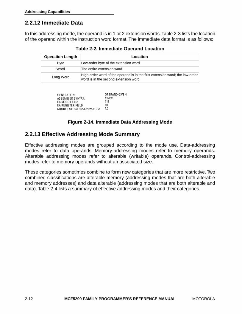
In this addressing mode, the operand is in 1 or 2 extension words. Table 2-3 lists the locationof the operand within the instruction word format. The immediate data format is as follows:
Figure 2-14. Immediate Data Addressing Mode
2.2.13 Effective Addressing Mode Summary
Effective addressing modes are grouped according to the mode use. Data-addressingmodes refer to data operands. Memory-addressing modes refer to memory operands.Alterable addressing modes refer to alterable (writable) operands. Control-addressingmodes refer to memory operands without an associated size.
These categories sometimes combine to form new categories that are more restrictive. Twocombined classifications are alterable memory (addressing modes that are both alterableand memory addresses) and data alterable (addressing modes that are both alterable anddata). Table 2-4 lists a summary of effective addressing modes and their categories.
Table 2-2. Immediate Operand Location
Operation Length Location
Byte Low-order byte of the extension word.
Word The entire extension word.
Long WordHigh-order word of the operand is in the first extension word; the low-order word is in the second extension word.
OPERAND GIVEN#<xxx>1111001,2,4, OR 6, EXCEPT FOR PACKED DECIMAL REAL OPERANDS
GENERATION:ASSEMBLER SYNTAX:EA MODE FIELD:EA REGISTER FIELD:NUMBER OF EXTENSION WORDS:

Addressing Capabilities
MOTOROLA
MCF5200 FAMILY PROGRAMMER’S REFERENCE MANUAL
2-13
2.3 STACK
Address register (A7) stacks exception frames, subroutine calls and returns, temporaryvariable storage, parameter passing, and is affected by instructions such as the LINK,UNLK, RTE, and PEA. To maximize performance, A7 must be long-word aligned at all times.Therefore, when modifying A7, be sure to do so in multiples of 4 to maintain alignment. Tofuther ensure alignment of A7 during exception handling, the ColdFire architectureimplements a self-aligning stack when processing exceptions.
Users can employ other address registers to implement other stacks using the addressregister indirect
with postincrement and predecrement addressing modes. With an addressregister, users can implement a stack that fills either from high memory to low memory orvice versa. Regarding the following important considerations, users should
• use the predecrement mode to decrement the register before using its contents as the pointer to the stack
• use the postincrement mode to increment the register after using its contents as the pointer to the stack
• maintain the stack pointer correctly when byte, word, and long-word items mix in these stacks
Table 2-3. Effective Addressing Modes and Categories
Addressing Modes SyntaxModeField
Reg.Field Data Memory Control Alterable
Register Direct Data Address
DnAn
000001
reg. no.reg. no.
X—
——
——
XX
Register IndirectAddressAddress with PostincrementAddress with PredecrementAddress with Displacement
(An)(An)+–(An)
(d
16
,An)
010011100101
reg. no.reg. no.reg. no.reg. no.
XXXX
XXXX
X——X
XXXX
Address Register Indirect with Index8-Bit Displacement (d
8
,An,Xn) 110 reg. no. X X X X
Program Counter Indirectwith Displacement (d
16
,PC) 111 010 X X X —
Program Counter Indirect with Index 8-Bit Displacement (d
8
,PC,Xn) 111 011 X X X —
Absolute Data Addressing ShortLong
(xxx).W(xxx).L
111111
000000
XX
XX
XX
——
Immediate #<xxx> 111 100 X X — —

Addressing Capabilities
2-14
MCF5200 FAMILY PROGRAMMER’S REFERENCE MANUAL
MOTOROLA
To implement stack growth from high memory to low memory, use -(An) to push data on thestack and (An) + to pull data from the stack. For this type of stack, after either a push or apull operation, the address register points to the top item on the stack.
Figure 2-15. Stack Growth from High Memory to Low Memory
To implement stack growth from low memory to high memory, use (An) + to push data onthe stack and -(An) to pull data from the stack. After either a push or pull operation, theaddress register points to the next available space on the stack.
Figure 2-16. Stack Growth from Low Memory to High Memory
BOTTOM OF STACK
LOW MEMORY(FREE)
TOP OF STACK
HIGH MEMORY
An
BOTTOM OF STACKLOW MEMORY
TOP OF STACK(FREE)
HIGH MEMORY
An

MOTOROLA
MCF5200 FAMILY PROGRAMMER’S REFERENCE MANUAL
3-1
SECTION 3INSTRUCTION SET SUMMARY
This section briefly describes the ColdFire Family instruction set, using Motorola’s assemblylanguage syntax and notation. It includes instruction set details such as notation and format,selected instruction examples, and an integer condition code discussion. The sectionconcludes with a discussion of conditional test definitions, an explanation of the operationtable, and postprocessing.
3.1 INSTRUCTION SUMMARY
Instructions form a set of tools that perform the following types of operations:
The following paragraphs describe in detail the instruction for each type of operation. Table3-1 lists the notations used throughout this manual. In the operand syntax statements of theinstruction definitions, the operand on the right is the destination operand.
Data Movement Program Control
Integer Arithmetic System Control
Logical Operations Shift Operations
Bit Manipulation

Instruction Set Summary
3-2
MCF5200 FAMILY PROGRAMMER’S REFERENCE MANUAL
MOTOROLA
Table 3-1. Notational Conventions
Single- And Double Operand Operations
+ Arithmetic addition or postincrement indicator.
– Arithmetic subtraction or predecrement indicator.
×
Arithmetic multiplication.
÷
Arithmetic division or conjunction symbol.
~ Invert; operand is logically complemented.
Λ
Logical AND
V
Logical OR
⊕
Logical exclusive OR
→
Source operand is moved to destination operand.
←→
Two operands are exchanged.
<op> Any double-operand operation.
<operand>tested Operand is compared to zero and the condition codes are set appropriately.
sign-extended All bits of the upper portion are made equal to the high-order bit of the lower portion.
Other Operations
TRAP SP - 4
→
SP; PC
→
(SP); SP - 2
→
SP; SR
→
(SP); SP - 2
→
SP; FORMAT
→
(SP); (Vector)
→
PC
STOP Enter the stopped state, waiting for interrupts.
If <condition>then <operations>else <operations>
Test the condition. If true, the operations after “then”are performed. If the condition is false and the optional “else”clause is present, the operations after “else”are performed. If the condition is false and else is omitted, the instruction performs no operation. Refer to the Bcc instruction description as an example.
Register Specifications
An Any Address Register n (example: A3 is address register 3)
Ax, Ay Source and destination address registers, respectively.
Dc Data register D7–D0, used during compare.
Dh, Dl Data register’s high- or low-order 32 bits of product.
Dn Any Data Register n (example: D5 is data register 5)
Dr, Dq Data register’s remainder or quotient of divide.
Du Data register D7–D0, used during update.
Dx, Dy Source and destination data registers, respectively.
MRn Any Memory Register n.
Rn Any Address or Data Register
Rx, Ry Any source and destination registers, respectively.
Xn Index Register

Instruction Set Summary
MOTOROLA
MCF5200 FAMILY PROGRAMMER’S REFERENCE MANUAL
3-3
Table 3-1. Notational Conventions (Continued)
Data Format And Type
<fmt> Operand Data Format: Byte (B), Word (W), Long (L)
B, W, L Specifies a signed integer data type (twos complement) of byte, word, or long word.
Subfields and Qualifiers
#<xxx> or #<data> Immediate data following the instruction word(s).
( ) Identifies an indirect address in a register.
[ ] Identifies an indirect address in memory.
d
n
Displacement Value, n Bits Wide (example: d
16
is a 16-bit displacement).
LSB Least Significant Bit
LSW Least Significant Word
MSB Most Significant Bit
MSW Most Significant Word
SIZE The index register’s size (W for word, L for long word).
Register Names
CCR Condition Code Register (lower byte of status register)
IC, DC, IC/DC Instruction, Data, or Both Caches
PC Program Counter
OC An or Dn Register
SR Status Register

Instruction Set Summary
3-4
MCF5200 FAMILY PROGRAMMER’S REFERENCE MANUAL
MOTOROLA
Table 3-1. Notational Conventions (Concluded)
Register Codes
* General Case
C Carry Bit in CCR
cc Condition Codes from CCR
FC Function Code
N Negative Bit in CCR
U Undefined, Reserved for Motorola Use.
V Overflow Bit in CCR
X Extend Bit in CCR
Z Zero Bit in CCR
— Not Affected or Applicable.
Miscellaneous
<ea> Effective Address
<label> Assemble Program Label
<list> List of registers, for example D3–D0.
m Bit m of an Operand
m–n Bits m through n of Operand

Instruction Set Summary
MOTOROLA
MCF5200 FAMILY PROGRAMMER’S REFERENCE MANUAL
3-5
3.1.1 Data Movement Instructions
The MOVE instruction with its associated addressing mode is the basic means oftransferring and storing addresses and data. MOVE instructions transfer byte, word, andlong-word operands from memory to memory, memory to register, register to memory, andregister to register. MOVE instructions transfer word and long-word operands and ensurethat only valid address manipulations are executed. In addition to the general MOVEinstructions, there are several special data movement instructions: MOVEM, MOVEQ, LEA,PEA, LINK, and UNLK.

Instruction Set Summary
3-6
MCF5200 FAMILY PROGRAMMER’S REFERENCE MANUAL
MOTOROLA
3.1.2 Integer Arithmetic Instructions
The integer arithmetic operations include 3 basic operations: ADD, SUB, and MUL. Theyalso include CMP, CLR, and NEG. The instruction set includes ADD, CMP, and SUBinstructions for both address and data operations with all operand sizes valid for dataoperations. Address operands consist of 16 or 32 bits. The CLR and NEG instructions applyto all sizes of data operands. Signed and unsigned MUL instruction includes
• word multiply to produce a long-word product
• long-word multiply to produce a long-word product
A set of extended instructions provides multiprecision and mixed-size arithmetic: ADDX,SUBX, EXT, and NEGX. Refer to Table 3-3 for a summary of the integer arithmeticoperations. In Table 3-3, X refers to the X-bit in the CCR.
Table 3-2. Data Movement Operation Format
Instruction Operand Syntax Operand Size Operation
LEA <ea>,An 32 <ea>
→
An
LINK An,#<data> 16 SP – 4
→
SP; An
→
(SP); SP
→
An, SP + D
→
SP
MOVEMOVEA
<ea>,<ea><ea>,An
8, 16, 3216, 32
→
32Source
→
Destination
MOVEM list,<ea><ea>,list
3232
Listed Registers
→
DestinationSource
→
Listed Registers
MOVEQ #<data>,Dn 8
→
32 Immediate Data
→
Destination
PEA <ea> 32 SP – 4
→
SP; <ea>
→
(SP)
UNLK An 32 An
→
SP; (SP)
→
An; SP + 4
→
SP

Instruction Set Summary
MOTOROLA
MCF5200 FAMILY PROGRAMMER’S REFERENCE MANUAL
3-7
Table 3-3. Integer Arithmetic Operation Format
Instruction Operand Syntax Operand Size Operation
ADD
ADDA
Dn,<ea><ea>,Dn<ea>,An
323232
Source + Destination
→
Destination
ADDIADDQ
#<data>,Dn#<data>,<ea>
3232
Immediate Data + Destination
→
Destination
ADDX Dy,Dx 32 Source + Destination + X
→
Destination
CLR <ea> 8, 16, 32 0
→
Destination
CMPCMPA
<ea>,Dn<ea>,An
3232
Destination – Source
CMPI #<data>, Dn 8, 16, 32 Destination – Immediate Data
EXT
EXTB
DnDnDn
8
→
1616
→
328
→
32
Sign-Extended Destination
→
Destination
MULS/MULU <ea>,Dn<ea>,Dl
16 x 16
→
3232 x 32
→
32Source x Destination
→
Destination(Signed or Unsigned)
NEG <ea> 32 0 – Destination
→
Destination
NEGX <ea> 32 0 – Destination – X
→
Destination
SUB
SUBA
<ea>,DnDn,<ea><ea>,An
323232
Destination = Source
→
Destination
SUBISUBQ
#<data>, Dn#<data>,<ea>
3232
Destination – Immediate Data
→
Destination
SUBX Dy,Dx 32 Destination – Source – X
→
Destination

Instruction Set Summary
3-8
MCF5200 FAMILY PROGRAMMER’S REFERENCE MANUAL
MOTOROLA
3.1.3 Logical Instructions
The instructions AND, OR, EOR, and NOT perform logical operations with all sizes of integerdata operands. A similar set of immediate instructions (ANDI, ORI, and EORI) providesthese logical operations with all sizes of immediate data. Table 3-4 summarizes the logicaloperations.
3.1.4 Shift Instruction
The ASR, ASL, LSR, and LSL instructions provide shift operations in both directions. All shiftoperations can be performed on either registers or memory.
Register shift operations shift all operand sizes. The shift count can be specified in theinstruction operation word (to shift from 1 – 8 places) or in a register (modulo 64 shift count).
Memory shift operations shift word operands one bit position only. The SWAP instructionexchanges the 16-bit halves of a register. Table 3-5 is a summary of the shift operations. InTable 3-5, C and X refer to the C-bit and X- bit in the CCR.
Table 3-4. Logical Operation Format
Instruction Operand Syntax Operand Size Operation
AND <ea>,DnDn,<ea>
3232
Source
Λ
Destination
→
Destination
ANDI #<data>, Dn 32 Immediate Data
Λ
Destination
→
Destination
EOR Dn,<ea> 32 Source
⊕
Destination
→
Destination
EORI #<data>, Dn 32 Immediate Data
⊕
Destination
→
Destination
NOT <ea> 32 ~ Destination
→
Destination
OR <ea>,DnDn,<ea>
32 Source
V
Destination
→
Destination
ORI #<data>, Dn 32 Immediate Data
V
Destination
→
Destination

Instruction Set Summary
MOTOROLA
MCF5200 FAMILY PROGRAMMER’S REFERENCE MANUAL
3-9
NOTE: X indicates the extend bit and C the carry bit in the CCR.
3.1.5 Bit Manipulation Instructions
BTST, BSET, BCLR, and BCHG are bit manipulation instructions. All bit manipulationoperations can be performed on either registers or memory. The bit number is specifiedeither as immediate data or in the contents of a data register. Register operands are 32 bitslong, and memory operands are 8 bits long. Table 3-6 summarizes bit manipulationoperations; Z refers to the zero bit of the CCR.
3.1.6 Program Control Instructions
A set of subroutine call-and-return instructions and conditional and unconditional branchinstructions perform program control operations. Also included are test operand instructions(TST), which set the integer condition codes for use by other program and system controlinstructions. NOP forces synchronization of the internal pipelines. Table 3-7 summarizesthese instructions.
Table 3–5. Shift Operation Format
Instruction Operand Syntax Operand Size Operation
ASL Dx, Dy# <data>, Dn
3232
ASR Dx, Dy#<data>, Dn
3232
LSL Dx, Dy#<data>, Dn
3232
LSR Dx, Dy#<data>, Dn
3232
SWAP Dn 16
Table 3-6. Bit Manipulation Operation Format
Instruction Operand Syntax Operand Size Operation
BCHG Dn,<ea>#<data>,<ea>
8, 328, 32
~ (<Bit Number> of Destination)
→
Z
→
Bit of Destination
BCLR Dn,<ea>#<data>,<ea>
8, 328, 32
~ (<Bit Number> of Destination)
→
Z;0
→
Bit of Destination
BSET Dn,<ea>#<data>,<ea>
8, 328, 32
~ (<Bit Number> of Destination)
→
Z;1
→
Bit of Destination
BTST Dn,<ea>#<data>,<ea>
8, 328, 32
~ (<Bit Number> of Destination)
→
Z
MSW LSW
X0
0
0
X/C
X/C
X/C
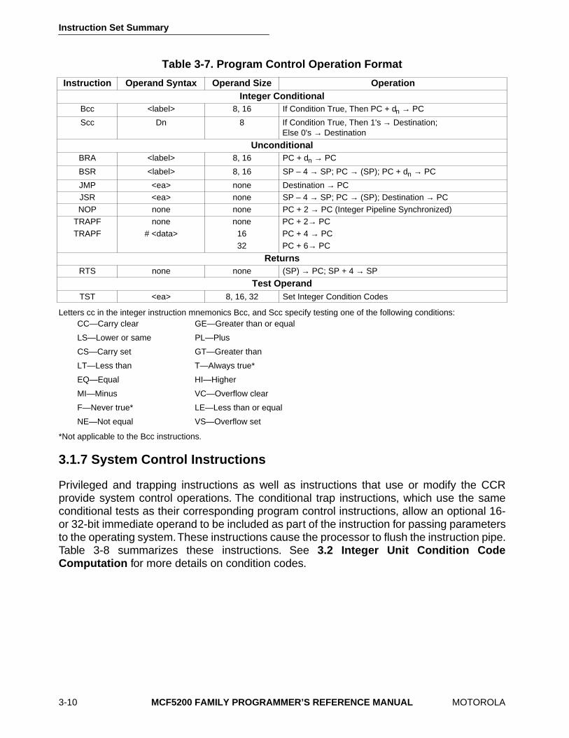
Instruction Set Summary
3-10
MCF5200 FAMILY PROGRAMMER’S REFERENCE MANUAL
MOTOROLA
Letters cc in the integer instruction mnemonics Bcc, and Scc specify testing one of the following conditions:
*Not applicable to the Bcc instructions.
3.1.7 System Control Instructions
Privileged and trapping instructions as well as instructions that use or modify the CCRprovide system control operations. The conditional trap instructions, which use the sameconditional tests as their corresponding program control instructions, allow an optional 16-or 32-bit immediate operand to be included as part of the instruction for passing parametersto the operating system. These instructions cause the processor to flush the instruction pipe.Table 3-8 summarizes these instructions. See 3.2 Integer Unit Condition CodeComputation for more details on condition codes.
Table 3-7. Program Control Operation Format
Instruction Operand Syntax Operand Size OperationInteger Conditional
Bcc <label> 8, 16 If Condition True, Then PC + dn → PC
Scc Dn 8 If Condition True, Then 1's → Destination;Else 0's → Destination
UnconditionalBRA <label> 8, 16 PC + dn → PC
BSR <label> 8, 16 SP – 4 → SP; PC → (SP); PC + dn → PC
JMP <ea> none Destination → PCJSR <ea> none SP – 4 → SP; PC → (SP); Destination → PCNOP none none PC + 2 → PC (Integer Pipeline Synchronized)
TRAPFTRAPF
none# <data>
none1632
PC + 2→ PCPC + 4 → PCPC + 6→ PC
ReturnsRTS none none (SP) → PC; SP + 4 → SP
Test OperandTST <ea> 8, 16, 32 Set Integer Condition Codes
CC—Carry clear GE—Greater than or equal
LS—Lower or same PL—Plus
CS—Carry set GT—Greater than
LT—Less than T—Always true*
EQ—Equal HI—Higher
MI—Minus VC—Overflow clear
F—Never true* LE—Less than or equal
NE—Not equal VS—Overflow set

Instruction Set Summary
MOTOROLA MCF5200 FAMILY PROGRAMMER’S REFERENCE MANUAL 3-11
3.2 INTEGER UNIT CONDITION CODE COMPUTATION
Many integer instructions affect the CCR to indicate the instruction’s results. Program andsystem control instructions also use certain combinations of these bits to control programand system flow. The condition codes meet consistency criteria across instructions, uses,and instances. They also meet the criteria of meaningful results, where no change occursunless it provides useful information.
Table 3-9 lists the integer condition code computations for instructions and Table 3-10 liststhe condition names, encodings, and tests for the conditional branch and set instructions.The test associated with each condition is a logical formula using the current states of thecondition codes. If this formula evaluates to one, the condition is true. If the formulaevaluates to zero, the condition is false. For example, the T condition is always true, and theEQ condition is true only if the Z-bit condition code is currently true.
Table 3-8. System Control Operation Format
Instruction Operand Syntax Operand Size Operation
Privileged
MOVE to SR Dn, SR, #<data>, SR
16 Source → SR Dn or #<data> source only
MOVE from SR Dn 16 SR → Destination
MOVEC Rn,Rc 32 Rn → Rc
RTE none none 2 (SP) → SR; 4 (SP) → PC; SP + 8 →SPAdjust Stack According to Format
STOP #<data> 16 Immediate Data → SR; STOP
HALT none none
WDEBUG <ea-2> 16
PULSE none none
WDDATA <ea> 8, 16, 32 Immediate Data → DDATA port
Trap Generating
TRAP none none SP – 4 → SP; PC → (SP);SP – 2 → SP; SR → (SP)SP – 2 → SP; Format → (SP)Vector Address → PC
Condition Code Register
MOVE to SR Dn, SR,SR #<data>
16 Source → CCR
MOVE from SR Dn 16 CCR → Destination

Instruction Set Summary
3-12 MCF5200 FAMILY PROGRAMMER’S REFERENCE MANUAL MOTOROLA
Table 3-9. Integer Unit Condition Code Computations
Operations X N Z V C Special Definition
ADD, ADDI, ADDQ * * * ? ? V = Sm Λ Dm Λ Rm V Sm Λ Dm Λ RmC = Sm Λ Dm V Rm Λ Dm V Sm Λ Rm
ADDX * * ? ? ? V = Sm Λ Dm Λ Rm V Sm Λ Dm Λ RmC = Sm Λ Dm V Rm Λ Dm V Sm Λ RmZ = Z Λ Rm Λ …Λ R0
AND, ANDI, EOR, EORI,MOVEQ, MOVE, OR, ORI,CLR, EXT, EXTB, NOT, TST
— * * 0 0
SUB, SUBI, SUBQ * * * ? ? V = Sm Λ Dm Λ Rm V Sm Λ Dm Λ RmC = Sm Λ Dm V Rm Λ Dm V Sm Λ Rm
SUBX * * ? ? ? V = Sm Λ Dm Λ Rm V Sm Λ Dm Λ RmC = Sm Λ Dm V Rm Λ Dm V Sm Λ RmZ = Z Λ Rm Λ …Λ R0
CMP, CMPA, CMPI — * * ? ? V = Sm Λ Dm Λ Rm V Sm Λ Dm Λ RmC = Sm Λ Dm V Rm Λ Dm V Sm Λ Rm
MULS, MULU — * * 0 0
NEG * * * ? ? V = Dm Λ RmC = Dm V Rm
NEGX * * ? ? ? V = Dm Λ RmC = Dm V RmZ = Z Λ Rm Λ …Λ R0
BTST, BCHG, BSET, BCLR — — ? — — Z = Dn
ASL * * * 0 ? C = Dm– r+1
ASL (r = 0) — * * 0 0
LSL * * * 0 ? C = Dm – r + 1

Instruction Set Summary
MOTOROLA MCF5200 FAMILY PROGRAMMER’S REFERENCE MANUAL 3-13
NOTES:N = Logical Not NV = Logical Not VZ = Logical Not Z*Not available for the Bcc instruction.
LSR (r = 0) — * * 0 0
ASR, LSR, ROXR * * * 0 ? C = Dr – 1
ASR, LSR (r = 0) — * * 0 0
? = Other—See Special Definition Rm = Result Operand (MSB)
N = Result Operand (MSB) Rm = Not Result Operand (MSB)
Z = Rm Λ…Λ R0 R = Register Tested
Sm = Source Operand (MSB) r = Shift Count
Dm = Destination Operand (MSB)
Table 3-10. Conditional Tests
Mnemonic Condition Encoding Test
T* True 0000 1
F* False 0001 0
HI High 0010 C Λ Z
LS Low or Same 0011 C V Z
CC(HI) Carry Clear 0100 C
CS(LO) Carry Set 0101 C
NE Not Equal 0110 Z
EQ Equal 0111 Z
VC Overflow Clear 1000 V
VS Overflow Set 1001 V
PL Plus 1010 N
MI Minus 1011 N
GE Greater or Equal 1100 N Λ V V N Λ V
LT Less Than 1101 N Λ V V N Λ V
GT Greater Than 1110 N Λ V Λ Z V N Λ V Λ Z
LE Less or Equal 1111 Z V N Λ V V N Λ V
Table 3-9. Integer Unit Condition Code Computations (Continued)
Operations X N Z V C Special Definition

Instruction Set Summary
3-14 MCF5200 FAMILY PROGRAMMER’S REFERENCE MANUAL MOTOROLA

MOTOROLA
MCF5200 FAMILY PROGRAMMER’S REFERENCE MANUAL
4-1
SECTION 4INTEGER INSTRUCTIONS
This section describes the integer instructions for the ColdFire Family. A detailed discussionof each instruction description is arranged in alphabetical order by instruction mnemonic.

Integer Instructions
4-2
MCF5200 FAMILY PROGRAMMER’S REFERENCE MANUAL
MOTOROLA
ADD
Add
ADD
Operation: Source + Destination
→
Destination
Assembler
ADD < ea > ,Dn
Syntax:
ADD Dn, < ea >
Attributes:
Size = Long
Description:
Adds the source operand to the destination operand using binary addition andstores the result in the destination location. The size of the operation may be specifiedas a long word. The mode of the instruction indicates which operand is the source andwhich is the destination as well as the operand size.
Condition Codes:
X — set the same as the carry bit N — set if the result is negative; cleared otherwise Z — set if the result is zero; cleared otherwise V — set if an overflow is generated; cleared otherwise C — set if a carry is generated; cleared otherwise
Instruction Format:
X N Z V C
∗ ∗ ∗ ∗ ∗
15 14 13 12 11 10 9 8 7 6 5 4 3 2 1 0
1 1 0 1 REGISTER OPMODEEFFECTIVE ADDRESS
MODE REGISTER

Integer Instructions
MOTOROLA
MCF5200 FAMILY PROGRAMMER’S REFERENCE MANUAL
4-3
ADD
Add
ADD
Instruction Fields:
Register field—specifies any of the 8 data registers.
Opmode field
Effective Address field—determines addressing mode
a. If the location <ea> specified is a source operand, use addressing modes listedin the following table:
Long Operation
010 < ea > + Dn 110 Dn + < ea >
→
< ea >
Addressing Mode Mode Register Addressing Mode Mode Register
Dn 000 reg. number:Dn (xxx).W 111 000
An 001 reg. number:An (xxx).L 111 001
(An) 010 reg. number:An #<data> 111 100
(An) + 011 reg. number:An
– (An) 100 reg. number:An
(d
16
,An) 101 reg. number:An (d
16
,PC) 111 010
(d
8
,An,Xn) 110 reg. number:An (d
8
,PC,Xn) 111 011

Integer Instructions
4-4
MCF5200 FAMILY PROGRAMMER’S REFERENCE MANUAL
MOTOROLA
ADD
Add
ADD
b. If the <ea> location specified is a destination operand, use only memory alterable addressing modes listed in the following table:
NOTE
The Dn mode is used when the destination is a data register; thedestination < ea > mode is invalid for a data register.
ADDA is used when the destination is an address register. ADDIand ADDQ are used when the source is immediate data.
Addressing Mode Mode Register Addressing Mode Mode Register
Dn — — (xxx).W 111 000
An — — (xxx).L 111 001
(An) 010 reg. number:An #<data> — —
(An) + 011 reg. number:An
– (An) 100 reg. number:An
(d
16
,An) 101 reg. number:An (d
16
,PC) — —
(d
8
,An,Xn) 110 reg. number:An (d
8
,PC,Xn) — —

Integer Instructions
MOTOROLA
MCF5200 FAMILY PROGRAMMER’S REFERENCE MANUAL
4-5
ADDA
Add Address
ADDA
Operation:
Source + Destination
→
Destination
Assembler Syntax:
ADDA < ea > , An
Attributes:
Size = Long
Description:
Adds the source operand to the destination address register and stores theresult in the address register. The size of the operation is specified as a long word.
Condition Codes:
Not affected
Instruction Format:
Instruction Fields:
Register field—specifies any of the 8 address registers (this is always the destination).
15 14 13 12 11 10 9 8 7 6 5 4 3 2 1 0
1 1 0 1 REGISTER 1 1 1EFFECTIVE ADDRESS
MODE REGISTER

Integer Instructions
4-6
MCF5200 FAMILY PROGRAMMER’S REFERENCE MANUAL
MOTOROLA
ADDA
Add Address
ADDA
Effective Address field—specifies the source operand; use addressing modes listed inthe following table:
Addressing Mode Mode Register Addressing Mode Mode Register
Dn 000 reg. number:Dn (xxx).W 111 000
An 001 reg. number:An (xxx).L 111 001
(An) 010 reg. number:An #<data> 111 100
(An) + 011 reg. number:An
– (An) 100 reg. number:An
(d
16
,An) 101 reg. number:An (d
16
,PC) 111 010
(d
8
,An,Xn) 110 reg. number:An (d
8
,PC,Xn) 111 011

Integer Instructions
MOTOROLA
MCF5200 FAMILY PROGRAMMER’S REFERENCE MANUAL
4-7
ADDI
Add Immediate
ADDI
Operation:
Immediate Data + Destination
→
Destination
Assembler Syntax:
ADDI # < data > , Dn
Attributes:
Size = Long
Description:
Adds the immediate data to the destination operand and stores the result inthe destination location. The size of the operation is specified as long word.
Condition Codes:
X — set the same as the carry bit N — set if the result is negative; cleared otherwise Z — set if the result is zero; cleared otherwise V — set if an overflow is generated; cleared otherwise C — set if a carry is generated; cleared otherwise
Instruction Format:
Instruction Fields:
Register field - specifies the destination data register.
X N Z V C
* * * * *
15 14 13 12 11 10 9 8 7 6 5 4 3 2 1 0
0 0 0 0 0 1 1 0 1 0 0 0 0REGISTER
UPPER WORD OF IMMEDIATE DATA
LOWER WORD OF IMMEDIATE DATA

Integer Instructions
4-8
MCF5200 FAMILY PROGRAMMER’S REFERENCE MANUAL
MOTOROLA
ADDQ
Add Quick
ADDQ
Operation:
Immediate Data + Destination
→
Destination
Assembler Syntax:
ADDQ # < data > , < ea >
Attributes:
Size = Long
Description:
Adds an immediate value of 1 to 8 to the operand at the destination location.The size of the operation is specified as long word. When adding to address registers,the condition codes are not altered and the entire destination address register is used.
Condition Codes:
X — set the same as the carry bit N — set if the result is negative; cleared otherwise Z — set if the result is zero; cleared otherwise V — set if an overflow occurs; cleared otherwise C — set if a carry occurs; cleared otherwise
The condition codes are not affected when the destination is an address register.
Instruction Format:
X N Z V C
* * * * *
15 14 13 12 11 10 9 8 7 6 5 4 3 2 1 0
0 1 0 1 DATA 0 1 0EFFECTIVE ADDRESS
MODE REGISTER

Integer Instructions
MOTOROLA
MCF5200 FAMILY PROGRAMMER’S REFERENCE MANUAL
4-9
ADDQ
Add Quick
ADDQ
Instruction Fields:
Data field—3 bits of immediate data representing 8 values (0 – 7), with the immediatevalue 0 representing a value of 8.
Effective Address field—specifies the destination location; use only those alterableaddressing modes listed in the following table:
Addressing Mode Mode Register Addressing Mode Mode Register
Dn 000 reg. number:Dn (xxx).W 111 000
An 001 reg. number:An (xxx).L 111 001
(An) 010 reg. number:An #<data> — —
(An) + 011 reg. number:An
– (An) 100 reg. number:An
(d
16
,An) 101 reg. number:An (d
16
,PC) — —
(d
8
,An,Xn) 110 reg. number:An (d
8
,PC,Xn) — —

Integer Instructions
4-10 MCF5200 FAMILY PROGRAMMER’S REFERENCE MANUAL MOTOROLA
ADDX Add Extended ADDX
Operation: Source + Destination + X → Destination
Assembler ADDX Dy,Dx
Attributes: Size = Long
Description: Adds the source operand and the extend bit to the destination operand andstores the result in the destination location. The operands can be addressed from dataregister to data register—where the data registers specified in the instruction containthe operands.
The size of the operation is specified as a long word.
Condition Codes:
X — set the same as the carry bit N — set if the result is negative; cleared otherwise Z — cleared if the result is nonzero; unchanged otherwise V — set if an overflow occurs; cleared otherwise C — set if a carry is generated; cleared otherwise
X N Z V C
* * * * *

Integer Instructions
MOTOROLA MCF5200 FAMILY PROGRAMMER’S REFERENCE MANUAL 4-11
ADDX Add Extended ADDX
Instruction Format:
Instruction Fields:
Register Rx field—specifies the destination data register.
Register Ry field—specifies the source data register.
15 14 13 12 11 10 9 8 7
1
6 5 4 3 2 1 0
1 1 0 1 REGISTER Rx 1 0 0 0 0 REGISTER Ry

Integer Instructions
4-12 MCF5200 FAMILY PROGRAMMER’S REFERENCE MANUAL MOTOROLA
AND AND Logical AND
Operation: Source L Destination → Destination
Assembler AND < ea > ,Dn Syntax: AND Dn, < ea >
Attributes: Size = Long
Description: Performs an AND operation of the source operand with the destinationoperand and stores the result in the destination location. The size of the operation isspecified as a long word. Address register contents may not be used as an operand.
Condition Codes:
X — not affected N — set if the most significant bit of the result is set; cleared otherwiseZ — set if the result is zero; cleared otherwise V — always cleared C — always cleared
Instruction Format:
Instruction Fields:
Register field—Specifies any of the 8 data registers.
Opmode field
X N Z V C — * * 0 0
15 14 13 12 11 10 9 8 7 6 5 4 3 2 1 0
1 1 0 0 REGISTER OPMODEEFFECTIVE ADDRESS
MODE REGISTER
Long Operation 010 < ea > Λ Dn → Dn 110 Dn Λ < ea > → < ea >

Integer Instructions
MOTOROLA MCF5200 FAMILY PROGRAMMER’S REFERENCE MANUAL 4-13
AND AND Logical AND
Effective Address field—determines addressing mode.
a. If the location specified is a source operand, use only those data addressingmodes listed in the following table:
Addressing Mode Mode Register Addressing Mode Mode Register
Dn 000 reg. number:Dn (xxx).W 111 000
An — — (xxx).L 111 001
(An) 010 reg. number:An #<data> 111 100
(An) + 011 reg. number:An
– (An) 100 reg. number:An
(d16,An) 101 reg. number:An (d16,PC) 111 010
(d8,An,Xn) 110 reg. number:An (d8,PC,Xn) 111 011

Integer Instructions
4-14 MCF5200 FAMILY PROGRAMMER’S REFERENCE MANUAL MOTOROLA
AND AND Logical AND
b. If the location specified is a destination operand, use only those memory alterableaddressing modes listed in the following table:
Addressing Mode Mode Register Addressing Mode Mode Register
Dn — — (xxx).W 111 000
An — — (xxx).L 111 001
(An) 010 reg. number:An #<data> — —
(An) + 011 reg. number:An
– (An) 100 reg. number:An
(d16,An) 101 reg. number:An (d16,PC) — —
(d8,An,Xn) 110 reg. number:An (d8,PC,Xn) — —

Integer Instructions
MOTOROLA MCF5200 FAMILY PROGRAMMER’S REFERENCE MANUAL 4-15
ANDI AND Immediate ANDI
Operation: Immediate Data Λ Destination → Destination
Assembler Syntax: ANDI # < data > , Dn
Attributes: Size = Long
Description: Performs an AND operation of the immediate data with the destinationoperand and stores the result in the destination location. The size of the operation isspecified as a long word. The size of the immediate data is specified as a long word.
Condition Codes:
X — not affected N — set if the most significant bit of the result is set; cleared otherwise Z — set if the result is zero; cleared otherwise V — always cleared C — always cleared
Instruction Format:
Instruction Fields:
Register field - specifies the destination data register.
X N Z V C — * * 0 0
15 14 13 12 11 10 9 8 7 6 5 4 3 2 1 0
0 0 0 0 0 0 1 0 1 0 0 0 0 REGISTER
UPPER WORD OF IMMEDIATE DATA
LOWER WORD OF IMMEDIATE DATA
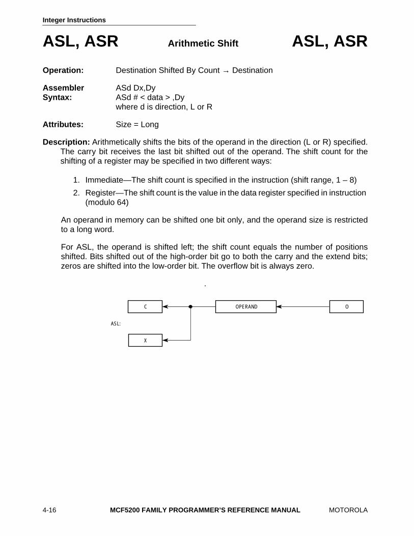
Integer Instructions
4-16 MCF5200 FAMILY PROGRAMMER’S REFERENCE MANUAL MOTOROLA
ASL, ASR Arithmetic Shift ASL, ASR
Operation: Destination Shifted By Count → Destination
Assembler ASd Dx,Dy Syntax: ASd # < data > ,Dy
where d is direction, L or R
Attributes: Size = Long
Description: Arithmetically shifts the bits of the operand in the direction (L or R) specified.The carry bit receives the last bit shifted out of the operand. The shift count for theshifting of a register may be specified in two different ways:
1. Immediate—The shift count is specified in the instruction (shift range, 1 – 8)
2. Register—The shift count is the value in the data register specified in instruction (modulo 64)
An operand in memory can be shifted one bit only, and the operand size is restrictedto a long word.
For ASL, the operand is shifted left; the shift count equals the number of positionsshifted. Bits shifted out of the high-order bit go to both the carry and the extend bits;zeros are shifted into the low-order bit. The overflow bit is always zero.
.
C OPERAND O
X
ASL:

Integer Instructions
MOTOROLA MCF5200 FAMILY PROGRAMMER’S REFERENCE MANUAL 4-17
ASL, ASR Arithmetic Shift ASL, ASR
For ASR, the operand is shifted right; the number of positions shifted equals the shiftcount. Bits shifted out of the low-order bit go to both the carry and the extend bits; thesign bit (MSB) is shifted into the high-order bit.
Condition Codes:
X — set according to the last bit shifted out of the operand; unaffected for a shift countof zero
N — set if the most significant bit of the result is set; cleared otherwise Z — set if the result is zero; cleared otherwise C — set according to the last bit shifted out of the operand; cleared for a shift count
of zeroV — always cleared
Instruction Format:
REGISTER SHIFTS
Instruction Fields:
Count/Register field—specifies shift count or register that contains the shift count: If i/r = 0, contains the shift count; values 1 – 7 represent counts of 1 – 7; a value of
zero represents a count of 8.
If i/r = 1, specifies the data register that contains the shift count (modulo 64).
X N Z V C
* * * 0 *
15 14 13 12 11 10 9 8 7 6 5 4 3 2 1 0
1 1 1 0COUNT
REGISTERdr 1 0 i/r 0 0 REGISTER
OPERAND C
X
ASR:
MSB

Integer Instructions
4-18 MCF5200 FAMILY PROGRAMMER’S REFERENCE MANUAL MOTOROLA
ASL, ASR Arithmetic Shift ASL, ASR
dr field—specifies the direction of the shift: 0 — shift right 1 — shift left
i/r field If i/r = 0, specifies immediate shift count If i/r = 1, specifies register shift count
Register field—specifies a data register to be shifted.

Integer Instructions
MOTOROLA MCF5200 FAMILY PROGRAMMER’S REFERENCE MANUAL 4-19
Bcc Branch Conditionally Bcc
Operation: If Condition True Then PC + dn → PC
Assembler Syntax: Bcc < label >
Attributes: Size = Word or Long
Description: If the specified condition is true, program execution continues at location (PC)+ displacement. The program counter contains the address of the instruction word forthe Bcc instruction, plus two. The displacement is a two’s-complement integer thatrepresents the relative distance in bytes from the current program counter to thedestination program counter. If the 8-bit displacement field in the instruction word is 0,a 16-bit displacement (the word immediately following the instruction) is used.Condition code cc specifies one of the following conditional tests (refer to Table 3-19 formore information on these conditional tests):
Condition Codes:
Not affected
Mnemonic Condition Mnemonic Condition
CC(HI) Carry Clear LS Low or Same
CS(LO) Carry Set LT Less Than
EQ Equal MI Minus
GE Greater or Equal NE Not Equal
GT Greater Than PL Plus
HI High VC Overflow Clear
LE Less or Equal VS Overflow Set
Integer Instructions
4-20 MCF5200 FAMILY PROGRAMMER’S REFERENCE MANUAL MOTOROLA
Bcc Branch Conditionally Bcc
Instruction Format:
Instruction Fields:
Condition field— binary code for one of the conditions listed in the table.
8-Bit Displacement field—two’s complement integer specifying the number of bytesbetween the branch instruction and the next instruction to be executed if thecondition is met.
16-Bit Displacement field—used for the displacement when the 8-bit displacement fieldcontains $00.
NOTE
A branch to the next immediate instruction automatically usesthe 16-bit displacement format because the 8-bit displacementfield contains $00 (zero offset).
15 14 13 12 11 10 9 8 7 6 5 4 3 2 1 0
0 1 1 0 CONDITION 8-BIT DISPLACEMENT
16-BIT DISPLACEMENT IF 8-BIT DISPLACEMENT = $00

Integer Instructions
MOTOROLA MCF5200 FAMILY PROGRAMMER’S REFERENCE MANUAL 4-21
BCHG Test a Bit and Change BCHG
Operation: TEST ( < number > of Destination) → Z; TEST ( < number > of Destination) → < bit number > of Destination
Assembler BCHG Dy, < ea > Syntax: BCHG # < data > , ea
Attributes: Size = Byte, Long
Description: Tests a bit in the destination operand and sets the Z-condition codeappropriately, then inverts the specified bit in the destination. When the destination is adata register, any of the 32 bits can be specified by the modulo 32-bit number. Whenthe destination is a memory location, the operation is a byte operation, and the bitnumber is modulo 8. In all cases, bit zero refers to the least significant bit. The bitnumber for this operation may be specified in either of two ways:
1. Immediate— bit number is specified in a second word of the instruction
2. Register— specified data register contains the bit number
Condition Codes:
X — not affectedN — not affected Z — set if the bit tested is zero; cleared otherwiseV — not affectedC — not affected
X N Z V C — — * — —

Integer Instructions
4-22 MCF5200 FAMILY PROGRAMMER’S REFERENCE MANUAL MOTOROLA
BCHG Test a Bit and Change BCHG
Instruction Format:
BIT NUMBER DYNAMIC, SPECIFIED IN A REGISTER
Instruction Fields:
Register field—specifies the data register that contains the bit number.
Effective Address field—specifies the destination location; use only those data alterableaddressing modes listed in the following table:
*Long only; all others are byte
15 14 13 12 11 10 9 8 7 6 5 4 3 2 1 0
0 0 0 0 REGISTER 1 0 1EFFECTIVE ADDRESS
MODE REGISTER
Addressing Mode Mode Register Addressing Mode Mode Register
Dy* 000 reg. number:Dn (xxx).W 111 000
An — — (xxx).L 111 001
(An) 010 reg. number:An #<data> — —
(An) + 011 reg. number:An
– (An) 100 reg. number:An
(d16,An) 101 reg. number:An (d16,PC) — —
(d8,An,Xn) 110 reg. number:An (d8,PC,Xn) — —

Integer Instructions
MOTOROLA MCF5200 FAMILY PROGRAMMER’S REFERENCE MANUAL 4-23
BCHG Test a Bit and Change BCHG
Instruction Format:
BIT NUMBER STATIC, SPECIFIED AS IMMEDIATE DATA
Instruction Fields:
Effective Address field—specifies the destination location; use only those data alterableaddressing modes listed in the following table:
*Long only; all others are byte
Bit Number field—specifies the bit number.
15 14 13 12 11 10 9 8 7 6 5 4 3 2 1 0
0 0 0 0 1 0 0 0 0 1EFFECTIVE ADDRESS
MODE REGISTER
0 0 0 0 0 0 0 0 BIT NUMBER
Addressing Mode Mode Register Addressing Mode Mode Register
Dy* 000 reg. number:Dn (xxx).W — —
An — — (xxx).L — —
(An) 010 reg. number:An #<data> — —
(An) + 011 reg. number:An
– (An) 100 reg. number:An
(d16,An) 101 reg. number:An (d16,PC) — —
(d8,An,Xn) — — (d8,PC,Xn) — —

Integer Instructions
4-24 MCF5200 FAMILY PROGRAMMER’S REFERENCE MANUAL MOTOROLA
BCLR Test a Bit and Clear BCLR
Operation: TEST ( < bit number > of Destination) → Z; 0 → < bit number > of Des-tination
Assembler BCLR Dy, < ea > Syntax: BCLR # < data > , < ea >
Attributes: Size = Byte, Long
Description: Tests a bit in the destination operand and sets the Z-condition codeappropriately, then clears the specified bit in the destination. When a data register isthe destination, any of the 32 bits can be specified by a modulo 32-bit number. Whena memory location is the destination, the operation is a byte operation, and the bitnumber is modulo 8. In all cases, bit zero refers to the least significant bit. The bitnumber for this operation can be specified in either of two ways:
1. Immediate— bit number is specified in a second word of the instruction
2. Register— specified data register contains the bit number
Condition Codes:
X — not affectedN — not affected Z — set if the bit tested is zero; cleared otherwiseV — not affected C — not affected
X N Z V C — — * — —

Integer Instructions
MOTOROLA MCF5200 FAMILY PROGRAMMER’S REFERENCE MANUAL 4-25
BCLR Test a Bit and Clear BCLR
Instruction Format:
BIT NUMBER DYNAMIC, SPECIFIED IN A REGISTER
Instruction Fields:
Register field—specifies the data register that contains the bit number.
Effective Address field—specifies the destination location; use only those dataalterable addressing modes listed in the following table:
*Word only; all others are byte
15 14 13 12 11 10 9 8 7 6 5 4 3 2 1 0
0 0 0 0 REGISTER 1 1 0EFFECTIVE ADDRESS
MODE REGISTER
Addressing Mode Mode Register Addressing Mode Mode Register
Dy* 000 reg. number:Dy (xxx).W 111 000
An — — (xxx).L 111 001
(An) 010 reg. number:An #<data> — —
(An) + 011 reg. number:An
– (An) 100 reg. number:An
(d16,An) 101 reg. number:An (d16,PC) — —
(d8,An,Xn) — — (d8,PC,Xn) — —

Integer Instructions
4-26 MCF5200 FAMILY PROGRAMMER’S REFERENCE MANUAL MOTOROLA
BCLR Test a Bit and Clear BCLR
Instruction Format:
BIT NUMBER STATIC, SPECIFIED AS IMMEDIATE DATA
Instruction Fields:
Effective Address field—specifies the destination location; use only those data alterableaddressing modes listed in the following table:
*Long only; all others are byte
Bit Number field—specifies the bit number.
15 14 13 12 11 10 9 8 7 6 5 4 3 2 1 0
0 0 0 0 1 0 0 0 1 0EFFECTIVE ADDRESS
MODE REGISTER
0 0 0 0 0 0 0 0 BIT NUMBER
Addressing Mode Mode Register Addressing Mode Mode Register
Dy* 000 reg. number:Dy (xxx).W — —
An — — (xxx).L — —
(An) 010 reg. number:An #<data> — —
(An) + 011 reg. number:An
– (An) 100 reg. number:An
(d16,An) 101 reg. number:An (d16,PC) — —
(d8,An,Xn) — — (d8,PC,Xn) — —

Integer Instructions
MOTOROLA MCF5200 FAMILY PROGRAMMER’S REFERENCE MANUAL 4-27
BRA Branch Always BRA
Operation: PC + dn → PC
Assembler Syntax: BRA < label >
Attributes: Size = Byte, Word
Description: Program execution continues at location (PC) + displacement. The programcounter contains the address of the instruction word of the BRA instruction, plus two.The displacement is a two’s complement integer that represents the relative distancein bytes from the current program counter to the destination program counter. If the 8-bit displacement field in the instruction word is 0, a 16-bit displacement (the wordimmediately following the instruction) is used.
Condition Codes:
Not affected
Instruction Format:
Instruction Fields:
8-Bit Displacement field—two’s complement integer specifying the number of bytesbetween the branch instruction and the next instruction to be executed.
16-Bit Displacement field—used for a larger displacement when the 8-bit displacementis equal to $00.
NOTE
A branch to the next immediate instruction automatically usesthe 16-bit displacement format because the 8-bit displacementfield contains $00 (zero offset).
15 14 13 12 11 10 9 8 7 6 5 4 3 2 1 0
0 1 1 0 0 0 0 0 8-BIT DISPLACEMENT
16-BIT DISPLACEMENT IF 8-BIT DISPLACEMENT = $00

Integer Instructions
4-28 MCF5200 FAMILY PROGRAMMER’S REFERENCE MANUAL MOTOROLA
BSET Test a Bit and Set BSET
Operation: TEST ( < bit number > of Destination) → Z; 1 → < bit number > of Des-tination
Assembler BSET Dn, < ea > Syntax: BSET # < data > , < ea-1 >
Attributes: Size = Byte, Long
Description: Tests a bit in the destination operand and sets the Z-condition codeappropriately, then sets the specified bit in the destination operand. When a dataregister is the destination, any of the 32 bits can be specified by a modulo 32-bitnumber. When a memory location is the destination, the operation is a byte operation,and the bit number is modulo 8. In all cases, bit 0 refers to the least significant bit. Thebit number for this operation can be specified in either of two ways:
1. Immediate— bit number is specified in the second word of the instruction
2. Register— specified data register contains the bit number
Condition Codes:
X — not affected N — not affected Z — set if the bit tested is zero; cleared otherwise V — not affected C — not affected
X N Z V C — — ∗ — —

Integer Instructions
MOTOROLA MCF5200 FAMILY PROGRAMMER’S REFERENCE MANUAL 4-29
BSET Test a Bit and Set BSET
Instruction Format:
BIT NUMBER DYNAMIC, SPECIFIED IN A REGISTER
Instruction Fields:
Register field—specifies the data register that contains the bit number.
Effective Address field—specifies the destination location; use only those dataalterable addressing modes listed in the following table:
*Long only; all others are byte
15 14 13 12 11 10 9 8 7 6 5 4 3 2 1 0
0 0 0 0 REGISTER 1 1 1EFFECTIVE ADDRESS
MODE REGISTER
Addressing Mode Mode Register Addressing Mode Mode Register
Dn* 000 reg. number:Dn (xxx).W 111 000
An — — (xxx).L 111 001
(An) 010 reg. number:An #<data> — —
(An) + 011 reg. number:An
– (An) 100 reg. number:An
(d16,An) 101 reg. number:An (d16,PC) — —
(d8,An,Xn) — — (d8,PC,Xn) — —

Integer Instructions
4-30 MCF5200 FAMILY PROGRAMMER’S REFERENCE MANUAL MOTOROLA
BSET Test a Bit and Set BSET
Instruction Format:
BIT NUMBER STATIC, SPECIFIED AS IMMEDIATE DATA
Instruction Fields:
Effective Address field—specifies the destination location; use only those data alterableaddressing modes listed in the following table:
*Long only; all others are byte
Bit Number field—specifies the bit number.
15 14 13 12 11 10 9 8 7 6 5 4 3 2 1 0
0 0 0 0 1 0 0 0 1 1EFFECTIVE ADDRESS
MODE REGISTER
0 0 0 0 0 0 0 BIT NUMBER
Addressing Mode Mode Register Addressing Mode Mode Register
Dn* 000 reg. number:Dn (xxx).W — —
An — — (xxx).L — —
(An) 010 reg. number:An #<data> — —
(An) + 011 reg. number:An
– (An) 100 reg. number:An
(d16,An) 101 reg. number:An (d16,PC) — —
(d8, An, Xn) — — (d8,PC,Xn) — —

Integer Instructions
MOTOROLA MCF5200 FAMILY PROGRAMMER’S REFERENCE MANUAL 4-31
BSR Branch to Subroutine BSR
Operation: SP – 4 → SP; PC → (SP); PC + dn → PC
Assembler Syntax: BSR < label >
Attributes: Size = Byte, Word
Description: Pushes the word address of the instruction immediately following the BSRinstruction onto the system stack. The program counter contains the address of theinstruction word, plus two. Program execution then continues at location (PC) +displacement. The displacement is a two’s complement integer that represents therelative distance in bytes from the current program counter to the destination programcounter. If the 8-bit displacement field in the instruction word is 0, a 16-bit displacement(the word immediately following the instruction) is used.
Condition Codes:
Not affected
Instruction Format:
15 14 13 12 11 10 9 8 7 6 5 4 3 2 1 0
0 1 1 0 0 0 0 1 8-BIT DISPLACEMENT
16-BIT DISPLACEMENT IF 8-BIT DISPLACEMENT = $00

Integer Instructions
4-32 MCF5200 FAMILY PROGRAMMER’S REFERENCE MANUAL MOTOROLA
BSR Branch to Subroutine BSR
Instruction Fields:
8-Bit Displacement field—two’s complement integer specifying the number of bytesbetween the branch instruction and the next instruction to be executed.
16-Bit Displacement field—used for a larger displacement when the 8-bit displacementis equal to $00.
NOTE
A branch to the next immediate instruction automatically usesthe 16-bit displacement format because the 8-bit displacementfield contains $00 (zero offset).

Integer Instructions
MOTOROLA MCF5200 FAMILY PROGRAMMER’S REFERENCE MANUAL 4-33
BTST Test a Bit BTST
Operation: TEST ( < bit number > of Destination) → Z
Assembler BTST Dn, < ea > Syntax: BTST # < data > , < ea >
Attributes: Size = Byte, Long
Description: Tests a bit in the destination operand and sets the Z-condition codeappropriately. When a data register is the destination, any of the 32 bits can bespecified by a modulo 32- bit number. When a memory location is the destination, theoperation is a byte operation, and the bit number is modulo 8. In all cases, bit 0 refersto the least significant bit. The bit number for this operation can be specified in either oftwo ways:
1. Immediate— bit number is specified in a second word of the instruction
2. Register— specified data register contains the bit number
Condition Codes:
X — not affected N — not affected Z — set if the bit tested is zero; cleared otherwise V — not affected C — not affected
X N Z V C — — ∗ — —

Integer Instructions
4-34 MCF5200 FAMILY PROGRAMMER’S REFERENCE MANUAL MOTOROLA
BTST Test a Bit BTST
Instruction Format:
BIT NUMBER DYNAMIC, SPECIFIED IN A REGISTER
Instruction Fields:
Register field—specifies the data register that contains the bit number.
Effective Address field—specifies the destination location; use only those dataaddressing modes listed in the following table:
*Long only; all others are byte
15 14 13 12 11 10 9 8 7 6 5 4 3 2 1 0
0 0 0 0 REGISTER 1 0 0EFFECTIVE ADDRESS
MODE REGISTER
Addressing Mode Mode Register Addressing Mode Mode Register
Dn* 000 reg. number:Dn (xxx).W 111 000
An — — (xxx).L 111 001
(An) 010 reg. number:An #<data> 111 100
(An) + 011 reg. number:An
– (An) 100 reg. number:An
(d16,An) 101 reg. number:An (d16,PC) 111 010
(d8,An,Xn) 110 reg. number:An (d8,PC,Xn) 111 011

Integer Instructions
MOTOROLA MCF5200 FAMILY PROGRAMMER’S REFERENCE MANUAL 4-35
BTST Test a Bit BTST
Instruction Format:
BIT NUMBER STATIC, SPECIFIED AS IMMEDIATE DATA
Instruction Fields:
Effective Address field—specifies the destination location; use only those dataaddressing modes listed in the following table:
Bit Number field—specifies the bit number.
15 14 13 12 11 10 9 8 7 6 5 4 3 2 1 0
0 0 0 0 1 0 0 0 0 0EFFECTIVE ADDRESS
MODE REGISTER
0 0 0 0 0 0 0 0 BIT NUMBER
Addressing Mode Mode Register Addressing Mode Mode Register
Dn 000 reg. number:Dn (xxx).W — —
An — — (xxx).L — —
(An) 010 reg. number:An #<data> — —
(An) + 011 reg. number:An
– (An) 100 reg. number:An
(d16,An) 101 reg. number:An (d16,PC) — —
(d8,An,Xn) — — (d8,PC,Xn) — —

Integer Instructions
4-36 MCF5200 FAMILY PROGRAMMER’S REFERENCE MANUAL MOTOROLA
CLR Clear an Operand CLR
Operation: 0 → Destination
Assembler Syntax: CLR < ea >
Attributes: Size = Byte, Word, Long
Description: Clears the destination operand to 0. The size of the operation may be specifiedas byte, word, or long.
Condition Codes:
X — not affected N — always cleared Z — always set V — always cleared C — always cleared
Instruction Format:
X N Z V C — 0 1 0 0
15 14 13 12 11 10 9 8 7 6 5 4 3 2 1 0
0 1 0 0 0 0 1 0 SIZEEFFECTIVE ADDRESS
MODE REGISTER

Integer Instructions
MOTOROLA MCF5200 FAMILY PROGRAMMER’S REFERENCE MANUAL 4-37
CLR Clear an Operand CLR
Instruction Fields:
Size field—specifies the size of the operation00— byte operation 01— word operation 10— long word operation
Effective Address field—specifies the destination location; use only those dataalterable addressing modes listed in the following table:
Addressing Mode Mode Register Addressing Mode Mode Register
Dn 000 reg. number:Dn (xxx).W 111 000
An — — (xxx).L 111 001
(An) 010 reg. number:An #<data> — —
(An) + 011 reg. number:An
– (An) 100 reg. number:An
(d16,An) 101 reg. number:An (d16,PC) — —
(d8,An,Xn) 110 reg. number:An (d8,PC,Xn) — —

Integer Instructions
4-38 MCF5200 FAMILY PROGRAMMER’S REFERENCE MANUAL MOTOROLA
CMP Compare CMP
Operation: Destination – Source → cc
Assembler Syntax: CMP < ea > , Dn
Attributes: Size = Long
Description: Subtracts the source operand from the destination data register and sets thecondition codes according to the result; the data register is not changed. The size ofthe operation is specified as a long word.
Condition Codes:
X — not affected N — set if the result is negative; cleared otherwise Z — set if the result is zero; cleared otherwiseV — set if an overflow occurs; cleared otherwise C — set if a borrow occurs; cleared otherwise
Instruction Format:
Instruction Fields:
Register field—specifies the destination data register.
X N Z V C — ∗ ∗ ∗ ∗
15 14 13 12 11 10 9 8 7 6 5 4 3 2 1 0
1 0 1 1 REGISTER 0 1 0EFFECTIVE ADDRESS
MODE REGISTER

Integer Instructions
MOTOROLA MCF5200 FAMILY PROGRAMMER’S REFERENCE MANUAL 4-39
CMP Compare CMP
Effective Address field—specifies the source operand; use addressing modes as listedin the following table:
Addressing Mode Mode Register Addressing Mode Mode Register
Dn 000 reg. number:Dn (xxx).W 111 000
An 001 reg. number:An (xxx).L 111 001
(An) 010 reg. number:An #<data> 111 100
(An) + 011 reg. number:An
– (An) 100 reg. number:An
(d16,An) 101 reg. number:An (d16,PC) 111 010
(d8,An,Xn) 110 reg. number:An (d8,PC,Xn) 111 011

Integer Instructions
4-40 MCF5200 FAMILY PROGRAMMER’S REFERENCE MANUAL MOTOROLA
CMPA Compare Address CMPA
Operation: Destination – Source → cc
Assembler Syntax: CMPA < ea > , An
Attributes: Size = Long
Description: Subtracts the source operand from the destination address register and setsthe condition codes according to the result. The address register is not changed. Thesize of the operation is specified as a long word. Word length source operands are sign-extended to 32 bits for comparison.
Condition Codes:
X — not affected N — set if the result is negative; cleared otherwiseZ — set if the result is zero; cleared otherwise V — set if an overflow is generated; cleared otherwise C — set if a borrow is generated; cleared otherwise
Instruction Format:
X N Z V C — ∗ ∗ ∗ ∗
15 14 13 12 11 10 9 8 7 6 5 4 3 2 1 0
1 0 1 1 REGISTER 1 1 1EFFECTIVE ADDRESS
MODE REGISTER

Integer Instructions
MOTOROLA MCF5200 FAMILY PROGRAMMER’S REFERENCE MANUAL 4-41
CMPA Compare Address CMPA
Instruction Fields:
Register field—specifies the destination address register.
Effective Address field—specifies the source operand; use addressing modes as listedin the following table:
Addressing Mode Mode Register Addressing Mode Mode Register
Dn 000 reg. number:Dn (xxx).W 111 000
An 001 reg. number:An (xxx).L 111 001
(An) 010 reg. number:An #<data> 111 100
(An) + 011 reg. number:An
– (An) 100 reg. number:An
(d16,An) 101 reg. number:An (d16,PC) 111 010
(d8,An,Xn) 110 reg. number:An (d8,PC,Xn) 111 011
Integer Instructions
4-42 MCF5200 FAMILY PROGRAMMER’S REFERENCE MANUAL MOTOROLA
CMPI Compare Immediate CMPI
Operation: Destination – Immediate Data → cc
Assembler Syntax: CMPI # < data > , Dn
Attributes: Size = Long
Description: Subtracts the immediate data from the destination operand and sets thecondition codes according to the result; the destination location is not changed. Thesize of the operation is specified as a long word. The size of the immediate data isspecified as a long word.
Condition Codes:
X — not affected N — set if the result is negative; cleared otherwise Z — set if the result is zero; cleared otherwise V — set if an overflow occurs; cleared otherwise C — set if a borrow occurs; cleared otherwise
Instruction Format:
Instruction Fields:
Register field - destination data register.
X N Z V C — ∗ ∗ ∗ ∗
15 14 13 12 11 10 9 8 7 6 5 4 3 2 1 0
0 0 0 0 1 1 0 0 1 0 0 0 0REGISTER
UPPER WORD
LOWER WORD
Integer Instructions
MOTOROLA MCF5200 FAMILY PROGRAMMER’S REFERENCE MANUAL 4-43
EOR Exclusive-OR Logical EOR
Operation: Source ⊕ Destination → Destination
Assembler Syntax: EOR Dn, < ea >
Attributes: Size = Long
Description: Performs an exclusive-OR operation on the destination operand using thesource operand and stores the result in the destination location. The size of theoperation is specified as a long word. The source operand must be a data register. Thedestination operand is specified in the effective address field.
Condition Codes:
X — not affected N — set if the most significant bit of the result is set; cleared otherwise Z — set if the result is zero; cleared otherwise V — always cleared C — always cleared
Instruction Format:
Instruction Fields:
Register field—specifies any of the 8 data registers.
X N Z V C — ∗ ∗ 0 0
15 14 13 12 11 10 9 8 7 6 5 4 3 2 1 0
1 0 1 1 REGISTER 1 1 0EFFECTIVE ADDRESS
MODE REGISTER

Integer Instructions
4-44 MCF5200 FAMILY PROGRAMMER’S REFERENCE MANUAL MOTOROLA
EOR Exclusive-OR Logical EOR
Effective Address field—specifies the destination operand. Use only those dataalterable addressing modes listed in the following table :
Addressing Mode Mode Register Addressing Mode Mode Register
Dn 000 reg. number:Dn (xxx).W 111 000
An — — (xxx).L 111 001
(An) 010 reg. number:An #<data> — —
(An) + 011 reg. number:An
– (An) 100 reg. number:An
(d16,An) 101 reg. number:An (d16,PC) — —
(d8,An,Xn) 110 reg. number:An (d8,PC,Xn) — —

Integer Instructions
MOTOROLA MCF5200 FAMILY PROGRAMMER’S REFERENCE MANUAL 4-45
EORI Exclusive-OR Immediate EORI
Operation: Immediate Data ⊕ Destination → Destination
Assembler Syntax: EORI # < data > , Dn
Attributes: Size = Long
Description: Performs an exclusive-OR operation on the destination operand using theimmediate data and the destination operand and stores the result in the destinationlocation. The size of the operation is specified as a long word.
Condition Codes:
X — not affected N — set if the most significant bit of the result is set; cleared otherwise Z — set if the result is zero; cleared otherwise V — always cleared C — always cleared
Instruction Format:
Instruction Fields:
Register field - destination data register.
X N Z V C — ∗ ∗ 0 0
15 14 13 12 11 10 9 8 7 6 5 4 3 2 1 0
0 0 0 0 1 0 1 0 1 0 0 0 0 REGISTER
UPPER WORD IMMEDIATE DATA
LOWER WORD IMMEDIATE DATA

Integer Instructions
4-46 MCF5200 FAMILY PROGRAMMER’S REFERENCE MANUAL MOTOROLA
EXT, EXTB Sign-Extend EXT, EXTB
Operation: Destination Sign-Extended → Destination
Assembler EXT.W Dn extend byte to word Syntax: EXT.L Dn extend word to long word
EXTB.L Dn extend byte to long word
Attributes: Size = Word, Long
Description: Extends a byte in a data register to a word or a long word, or a word in a dataregister to a long word, by replicating the sign bit to the left. When the operation extendsa word to a long word, bit 15 of the designated data register is copied to bits 31 – 16 ofthe data register. The EXTB form copies bit 7 of the designated register to bits 31 – 8of the data register.
Condition Codes:
X — not affected N — set if the result is negative; cleared otherwise Z — set if the result is zero; cleared otherwise V — always cleared C — always cleared
Instruction Format:
Instruction Fields:
Opmode field—specifies the size of the sign-extension operation: 010—sign-extend low-order byte of data register to word 011—sign-extend low-order word of data register to long111—sign-extend low-order byte of data register to long
Register field—specifies that the data register is to be sign-extended.
X N Z V C — ∗ ∗ 0 0
15 14 13 12 11 10 9 8 7 6 5 4 3 2 1 0
0 1 0 0 1 0 0 OPMODE 0 0 0 REGISTER

Integer Instructions
MOTOROLA MCF5200 FAMILY PROGRAMMER’S REFERENCE MANUAL 4-47
JMP Jump JMP
Operation: Destination Address → PC
Assembler Syntax: JMP < ea >
Attributes: Unsized
Description: Program execution continues at the effective address specified by theinstruction. The addressing mode for the effective address must be a controladdressing mode.
Condition Codes:
Not affected
Instruction Format:
Instruction Field:
Effective Address field—specifies the address of the next instruction; use only thosecontrol addressing modes listed in the following table:
15 14 13 12 11 10 9 8 7 6 5 4 3 2 1 0
0 1 0 0 1 1 1 0 1 1EFFECTIVE ADDRESS
MODE REGISTER
Addressing Mode Mode Register Addressing Mode Mode Register
Dn — — (xxx).W 111 000
An — — (xxx).L 111 001
(An) 010 reg. number:An #<data> — —
(An) + — —
– (An) — —
(d16,An) 101 reg. number:An (d16,PC) 111 010
(d8,An,Xn) 110 reg. number:An (d8,PC,Xn) 111 011

Integer Instructions
4-48 MCF5200 FAMILY PROGRAMMER’S REFERENCE MANUAL MOTOROLA
JSR Jump to Subroutine JSR
Operation: SP – 4 → Sp; PC → (SP); Destination Address → PC
Assembler Syntax: JSR < ea >
Attributes: Unsized
Description: Pushes the long-word address of the instruction immediately following theJSR instruction onto the system stack. Program execution then continues at theaddress specified in the instruction.
Condition Codes:
Not affected
Instruction Format:
Instruction Field:
Effective Address field—specifies the address of the next instruction; use only thosecontrol addressing modes listed in the following table:
15 14 13 12 11 10 9 8 7 6 5 4 3 2 1 0
0 1 0 0 1 1 1 0 1 0EFFECTIVE ADDRESS
MODE REGISTER
Addressing Mode Mode Register Addressing Mode Mode Register
Dn — — (xxx).W 111 000
An — — (xxx).L 111 001
(An) 010 reg. number:An #<data> — —
(An) + — —
– (An) — —
(d16,An) 101 reg. number:An (d16,PC) 111 010
(d8,An,Xn) 110 reg. number:An (d8,PC,Xn) 111 011

Integer Instructions
MOTOROLA MCF5200 FAMILY PROGRAMMER’S REFERENCE MANUAL 4-49
LEA Load Effective Address LEA
Operation: < ea > → An
Assembler Syntax: LEA < ea > ,An
Attributes: Size = Long
Description: Loads the effective address into the specified address register. This instructionaffects all 32 bits of the address register.
Condition Codes:
Not affected
Instruction Format:
Instruction Fields:
Register field—specifies the address register to be updated with the effective address.
Effective Address field—specifies the address to be loaded into the address register;use only those control addressing modes listed in the following table:
15 14 13 12 11 10 9 8 7 6 5 4 3 2 1 0
0 1 0 0 REGISTER 1 1 1EFFECTIVE ADDRESS
MODE REGISTER
Addressing Mode Mode Register Addressing Mode Mode Register
Dn — — (xxx).W 111 000
An — — (xxx).L 111 001
(An) 010 reg. number:An #<data> — —
(An) + — —
– (An) — —
(d16,An) 101 reg. number:An (d16,PC) 111 010
(d8,An,Xn) 110 reg. number:An (d8,PC,Xn) 111 011
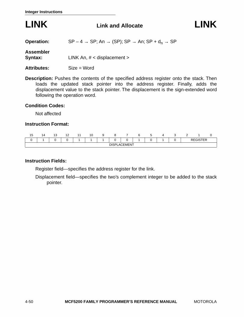
Integer Instructions
4-50 MCF5200 FAMILY PROGRAMMER’S REFERENCE MANUAL MOTOROLA
LINK Link and Allocate LINK
Operation: SP – 4 → SP; An → (SP); SP → An; SP + dn → SP
Assembler Syntax: LINK An, # < displacement >
Attributes: Size = Word
Description: Pushes the contents of the specified address register onto the stack. Thenloads the updated stack pointer into the address register. Finally, adds thedisplacement value to the stack pointer. The displacement is the sign-extended wordfollowing the operation word.
Condition Codes:
Not affected
Instruction Format:
Instruction Fields:
Register field—specifies the address register for the link.
Displacement field—specifies the two’s complement integer to be added to the stackpointer.
15 14 13 12 11 10 9 8 7 6 5 4 3 2 1 0
0 1 0 0 1 1 1 0 0 1 0 1 0 REGISTER
DISPLACEMENT

Integer Instructions
MOTOROLA MCF5200 FAMILY PROGRAMMER’S REFERENCE MANUAL 4-51
LSL, LSR Logical Shift LSL, LSR
Operation: Destination Shifted By Count → Destination
Assembler LSd Dx,Dy Syntax: LSd # < data > ,Dy
where d is direction, L or R
Attributes: Size = Long
Description: Shifts the bits of the operand in the direction specified (L or R). The carry bitreceives the last bit shifted out of the operand. The shift count for the shifting of aregister is specified in two different ways:
1. Immediate— shift count (1 – 8) is specified in the instruction
2. Register— shift count is the value in the data register specified in the instruction modulo 64
The LSL instruction shifts the operand to the left the number of positions specified asthe shift count. Bits shifted out of the high-order bit go to both the carry and the extendbits; zeros are shifted into the low-order bit.
.
The LSR instruction shifts the operand to the right the number of positions specified asthe shift count. Bits shifted out of the low-order bit go to both the carry and the extendbits; zeros are shifted into the high-order bit.
.
C OPERAND O
X
LSL:
O OPERAND C
X
LSR:

Integer Instructions
4-52 MCF5200 FAMILY PROGRAMMER’S REFERENCE MANUAL MOTOROLA
LSL, LSR Logical Shift LSL, LSR
Condition Codes:
X — set according to the last bit shifted out of the operand; unaffected for a shift countof zero
N — set if the result is negative; cleared otherwise Z — set if the result is zero; cleared otherwise V — always cleared C — set according to the last bit shifted out of the operand; cleared for a shift count
of zero
Instruction Format:
REGISTER SHIFTS
Instruction Fields:
Count/Register field
If i/r = 0, this field contains the shift count; values 1 – 7 represent shifts of 1 – 7; valueof 0 specifies shift count of 8
If i/r = 1, data register specified in this field contains shift count (modulo 64)
dr field—specifies the direction of the shift: 0 — shift right 1 — shift left
Register field—specifies a data register to be shifted.
I/R field0 — immediate shift count1 — register shift count
X N Z V C ∗ ∗ ∗ 0 ∗
15 14 13 12 11 10 9 8 7 6 5 4 3 2 1 0
1 1 1 0COUNT/
REGISTERdr 1 0 i/r 0 1 REGISTER
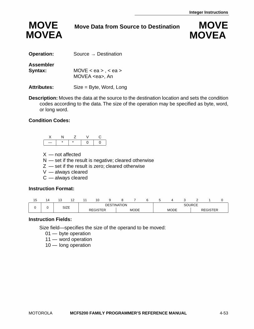
Integer Instructions
MOTOROLA MCF5200 FAMILY PROGRAMMER’S REFERENCE MANUAL 4-53
MOVE Move Data from Source to Destination MOVE
Operation: Source → Destination
Assembler Syntax: MOVE < ea > , < ea >
MOVEA <ea>, An
Attributes: Size = Byte, Word, Long
Description: Moves the data at the source to the destination location and sets the conditioncodes according to the data. The size of the operation may be specified as byte, word,or long word.
Condition Codes:
X — not affected N — set if the result is negative; cleared otherwise Z — set if the result is zero; cleared otherwise V — always cleared C — always cleared
Instruction Format:
Instruction Fields:
Size field—specifies the size of the operand to be moved: 01 — byte operation 11 — word operation 10 — long operation
X N Z V C — ∗ ∗ 0 0
15 14 13 12 11 10 9 8 7 6 5 4 3 2 1 0
0 0 SIZEDESTINATION SOURCE
REGISTER MODE MODE REGISTER
MOVEA MOVEA

Integer Instructions
4-54 MCF5200 FAMILY PROGRAMMER’S REFERENCE MANUAL MOTOROLA
MOVE Move Data from Source to Destination MOVE
Destination Effective Address field—specifies the destination location; the possibledata alterable addressing modes are listed in the table below. The ColdFire MOVEinstruction has restrictions on combinations of source and destination addressingmodes. The table shown on the bottom of page 4-55 outlines the restrictions.
*If the destination is an address register, condition codes are unaffected. Some assemblers acceptthe MOVEA mneumonic to designate this slight difference.
Addressing Mode Mode Register Addressing Mode Mode Register
Dn 000 reg. number:Dn (xxx).W 111 000
An* 001 reg. number: An (xxx).L 111 001
(An) 010 reg. number:An #<data> — —
(An) + 011 reg. number:An
– (An) 100 reg. number:An
(d16,An) 101 reg. number:An (d16,PC) — —
(d8,An,Xn) 110 reg. number:An (d8,PC,Xn) — —
MOVEA MOVEA

Integer Instructions
MOTOROLA MCF5200 FAMILY PROGRAMMER’S REFERENCE MANUAL 4-55
MOVE Move Data from Source to Destination MOVE
Source Effective Address field—specifies the source operand; the possible addressingmodes are listed in the table below. The ColdFire MOVE instruction hasrestrictions on combinations of source and destination addressing modes. Thetable shown on the bottom of this page outlines the restrictions.
NOTE
Most assemblers use MOVEA when the destination is anaddress register.
Use MOVEQ to move an immediate 8-bit value to a data register.
Not all combinations of source/destination addressing modesare possible. The table below shows the possible combinations.
Refere to the previous tables for valid source and destinationaddressing modes.
Addressing Mode Mode Register Addressing Mode Mode Register
Dn 000 reg. number:Dn (xxx).W 111 000
An 001 reg. number:An (xxx).L 111 001
(An) 010 reg. number:An #<data> 111 100
(An) + 011 reg. number:An
– (An) 100 reg. number:An
(d16,An) 101 reg. number:An (d16,PC) 111 010
(d8,An,Xn) 110 reg. number:An (d8,PC,Xn) 111 011
Source Addressing Mode Destination Addressing Mode
Dn, An, (An), (An)+,-(An) All possible
(d16, An), (d16, PC) All possible except (d8, An, Xn), (xxx).W, (xxx).L
(d8, An, Xn), (d8, PC, Xn), (xxx).W, (xxx).L, #<xxx>All possible except (d8, An, Xn), (d16, An), (xxx).W,
(xxx).L
MOVEA MOVEA

Integer Instructions
4-56 MCF5200 FAMILY PROGRAMMER’S REFERENCE MANUAL MOTOROLA
MOVE MOVE from CCR Move from the from CCR
Condition Code Register
Operation: CCR → Destination
Assembler Syntax: MOVE CCR, Dn
Attributes: Size = Word
Description: Moves the condition code bits (zero-extended to word size) to the destinationlocation. The operand size is a word. Unimplemented bits are read as zeros.
Condition Codes:
Not affected
Instruction Format:
Instruction Fields:
Register field - destination data register.
15 14 13 12 11 10 9 8 7 6 5 4 3 2 1 0
0 1 0 0 0 0 1 0 1 1 0 0 0 Register

Integer Instructions
MOTOROLA MCF5200 FAMILY PROGRAMMER’S REFERENCE MANUAL 4-57
MOVE MOVE to CCR Move to Condition Code Register to CCR
Operation: Source → CCR
Assembler Syntax: MOVE, Dn ,CCR
MOVE #<data>, CCR
Attributes: Size = Word
Description: Moves the low-order byte of the source operand to the condition code register.The upper byte of the source operand is ignored; the upper byte of the status registeris not altered.
Condition Codes:
X — set to the value of bit 4 of the source operand N — set to the value of bit 3 of the source operand Z — set to the value of bit 2 of the source operand V — set to the value of bit 1 of the source operandC — set to the value of bit 0 of the source operand
Instruction Format:
X N Z V C ∗ ∗ ∗ ∗ ∗
15 14 13 12 11 10 9 8 7 6 5 4 3 2 1 0
0 1 0 0 0 1 0 0 1 1EFFECTIVE ADDRESS
MODE REGISTER

Integer Instructions
4-58 MCF5200 FAMILY PROGRAMMER’S REFERENCE MANUAL MOTOROLA
MOVE MOVE to CCR Move to Condition Code Register to CCR
Instruction Field:
Effective Address field—specifies the location of the source operand; use only thosedata addressing modes listed in the following table:
Addressing Mode Mode Register Addressing Mode Mode Register
Dn 000 reg. number:Dn (xxx).W — —
An — — (xxx).L — —
(An) — — #<data> 111 100
(An) + — —
– (An) — —
(d16,An) — — (d16,PC) — —
(d8,An,Xn) — — (d8,PC,Xn) — —

Integer Instructions
MOTOROLA MCF5200 FAMILY PROGRAMMER’S REFERENCE MANUAL 4-59
MOVEM Move Multiple Registers MOVEM
Operation: Registers → Destination; Source → Registers
Assembler MOVEM < list > , < ea > Syntax: MOVEM < ea > , < list >
Attributes: Size = Long
Description: Moves the contents of selected registers to or from consecutive memorylocations starting at the location specified by the effective address. A register isselected if the bit in the mask field corresponding to that register is set.
The registers are transferred starting at the specified address, and the address is incre-mented by the operand length (4) following each transfer. The order of the registers isfrom D0 to D7, then from A0 to A7.

Integer Instructions
4-60 MCF5200 FAMILY PROGRAMMER’S REFERENCE MANUAL MOTOROLA
MOVEM Move Multiple Registers MOVEM
Condition Codes:
Not affected
Instruction Format:
Instruction Fields:
dr field—specifies the direction of the transfer: 0 — register to memory 1 — memory to register
Effective Address field—specifies the memory address for register-to-memorytransfers.
15 14 13 12 11 10 9 8 7 6 5 4 3 2 1 0
0 1 0 0 1 dr 0 0 1 1EFFECTIVE ADDRESS
MODE REGISTER
REGISTER LIST MASK
Addressing Mode Mode Register Addressing Mode Mode Register
Dn — — (xxx).W — —
An — — (xxx).L — —
(An) 010 reg. number:An #<data> — —
(An) + — —
– (An) — —
(d16,An) 101 reg. number:An (d16,PC) — —
(d8,An,Xn) — — (d8,PC,Xn) — —

Integer Instructions
MOTOROLA MCF5200 FAMILY PROGRAMMER’S REFERENCE MANUAL 4-61
MOVEM Move Multiple Registers MOVEM
For memory-to-register transfers, use addressing modes listed in the following tables:
Register List Mask field—specifies the registers to be transferred. The low-order bitcorresponds to the first register to be transferred; the high-order bit correspondsto the last register to be transferred. The mask correspondence is shown below.
Addressing Mode Mode Register Addressing Mode Mode Register
Dn — — (xxx).W — —
An — — (xxx).L — —
(An) 010 reg. number:An #<data> — —
(An) + — —
– (An) — —
(d16,An) 101 reg. number:An (d16,PC) — —
(d8,An,Xn) — — (d8,PC,Xn) — —
15 14 13 12 11 10 9 8 7 6 5 4 3 2 1 0
A7 A6 A5 A4 A3 A2 A1 A0 D7 D6 D5 D4 D3 D2 D1 D0

Integer Instructions
4-62 MCF5200 FAMILY PROGRAMMER’S REFERENCE MANUAL MOTOROLA
MOVEQ Move Quick MOVEQ
Operation: Immediate Data → Destination
Assembler Syntax: MOVEQ # < data > ,Dn
Attributes: Size = Long
Description: Moves a byte of immediate data to a 32-bit data register. The data in an 8-bitfield within the operation word is sign- extended to a long operand in the data registeras it is transferred.
Condition Codes:
X — not affected N — set if the result is negative; cleared otherwise Z — set if the result is zero; cleared otherwise V — always cleared C — always cleared
Instruction Format:
Instruction Fields:
Register field—specifies the data register to be loaded.
Data field—8 bits of data, which are sign-extended to a long operand.
X N Z V C — ∗ ∗ 0 0
15 14 13 12 11 10 9 8 7 6 5 4 3 2 1 0
0 1 1 1 REGISTER 0 DATA

Integer Instructions
MOTOROLA MCF5200 FAMILY PROGRAMMER’S REFERENCE MANUAL 4-63
MULS Signed Multiply MULS
Operation: Source x Destination → Destination
Assembler MULS.W < ea > ,Dn 16 x 16 → 32 Syntax: MULS.L < ea > ,Dl 32 x 32 → 32
Attributes: Size = Word, Long
Description: Multiplies two signed operands yielding a signed result. This instruction has aword operand form and a long operand form.
In the word form, the multiplier and multiplicand are both word operands, and the resultis a long-word operand. A register operand is the low-order word; the upper word of theregister is ignored. All 32 bits of the product are saved in the destination data register.
In the long form, the multiplier and multiplicand are both long word operands. The des-tination data register stores the low order 32-bits with the product. The upper 32 bits ofthe product are discarded.
Condition Codes:
X — not affected N — set if the result is negative; cleared otherwise Z — set if the result is zero; cleared otherwise V — always clearedC — always cleared
X N Z V C — ∗ ∗ 0 0

Integer Instructions
4-64 MCF5200 FAMILY PROGRAMMER’S REFERENCE MANUAL MOTOROLA
MULS Signed Multiply MULS
Instruction Format:
WORD
Instruction Fields:
Register field—specifies a data register as the destination.
Effective Address field—specifies the source operand; use only those data addressingmodes listed in the following table:
15 14 13 12 11 10 9 8 7 6 5 4 3 2 1 0
1 1 0 0 REGISTER 1 1 1EFFECTIVE ADDRESS
MODE REGISTER
Addressing Mode Mode Register Addressing Mode Mode Register
Dn 000 reg. number:Dn (xxx).W 111 000
An — — (xxx).L 111 001
(An) 010 reg. number:An #<data> 111 100
(An) + 011 reg. number:An
– (An) 100 reg. number:An
(d16,An) 101 reg. number:An (d16,PC) 111 010
(d8,An,Xn) 110 reg. number:An (d8,PC,Xn) 111 011

Integer Instructions
MOTOROLA MCF5200 FAMILY PROGRAMMER’S REFERENCE MANUAL 4-65
MULS Signed Multiply MULS
Instruction Format:
LONG
Instruction Fields:
Effective Address field—specifies the source operand; use only data addressing modeslisted in the following table:
Register Dl field—specifies a data register for the destination operand; the 32-bitmultiplicand comes from this register, and the low-order 32 bits of the product areloaded into this register.
15 14 13 12 11 10 9 8 7 6 5 4 3 2 1 0
0 1 0 0 1 1 0 0 0 0EFFECTIVE ADDRESS
MODE REGISTER
0 REGISTER DI 1 0 0 0 0 0 0 0 0 0 0 0
Addressing Mode Mode Register Addressing Mode Mode Register
Dn 000 reg. number:Dn (xxx).W — —
An — — (xxx).L — —
(An) 010 reg. number:An #<data> — —
(An) + 011 reg. number:An
– (An) 100 reg. number:An
(d16,An) 101 reg. number:An (d16,PC) — —
(d8,An,Xn) — — (d8,PC,Xn) — —

Integer Instructions
4-66 MCF5200 FAMILY PROGRAMMER’S REFERENCE MANUAL MOTOROLA
MULU Unsigned Multiply MULU
Operation: Source x Destination → Destination
Assembler MULU.W < ea > ,Dn 16 x 16 → 32 Syntax: MULU.L < ea > ,Dl 32 x 32 → 32
Attributes: Size = Word, Long
Description: Multiplies two unsigned operands yielding an unsigned result. This instructionhas a word operand form and a long operand form.
In the word form, the multiplier and multiplicand are both word operands, and the resultis a long-word operand. A register operand is the low-order word; the upper word of theregister is ignored. All 32 bits of the product are saved in the destination data register.
In the long form, the multiplier and multiplicand are both long- word operands, and thedestination data register stores the low order 32 bits of the product. The upper 32 bitsof the product are discarded.
Condition Codes:
X — not affected N — set if the result is negative; cleared otherwise Z — set if the result is zero; cleared otherwise V — always clearedC — always cleared
X N Z V C — ∗ ∗ 0 0

Integer Instructions
MOTOROLA MCF5200 FAMILY PROGRAMMER’S REFERENCE MANUAL 4-67
MULU Unsigned Multiply MULU
Instruction Format:
WORD
Instruction Fields:
Register field—specifies a data register as the destination.
Effective Address field—specifies the source operand; use only those data addressingmodes listed in the following table:
15 14 13 12 11 10 9 8 7 6 5 4 3 2 1 0
1 1 0 0 REGISTER 0 1 1EFFECTIVE ADDRESS
MODE REGISTER
Addressing Mode Mode Register Addressing Mode Mode Register
Dn 000 reg. number:Dn (xxx).W 111 000
An — — (xxx).L 111 001
(An) 010 reg. number:An #<data> 111 100
(An) + 011 reg. number:An
– (An) 100 reg. number:An
(d16,An) 101 reg. number:An (d16,PC) 111 010
(d8,An,Xn) 110 reg. number:An (d8,PC,Xn) 111 011

Integer Instructions
4-68 MCF5200 FAMILY PROGRAMMER’S REFERENCE MANUAL MOTOROLA
MULU Unsigned Multiply MULU
Instruction Format:
LONG
Instruction Fields:
Effective Address field—specifies the source operand; use only data addressing modeslisted in the following table:
Register Dl field—specifies a data register for the destination operand; the 32-bitmultiplicand comes from this register, and the low-order 32 bits of the product areloaded into this register.
15 14 13 12 11 10 9 8 7 6 5 4 3 2 1 0
0 1 0 0 1 1 0 0 0 0EFFECTIVE ADDRESS
MODE REGISTER
0 REGISTER Dl 0 0 0 0 0 0 0 0 0 0 0 0
Addressing Mode Mode Register Addressing Mode Mode Register
Dn 000 reg. number:Dn (xxx).W — —
An — — (xxx).L — —
(An) 010 reg. number:An #<data> — —
(An) + 011 reg. number:An
– (An) 100 reg. number:An
(d16,An) 101 reg. number:An (d16,PC) — —
(d8,An,Xn) — — (d8,PC,Xn) — —

Integer Instructions
MOTOROLA MCF5200 FAMILY PROGRAMMER’S REFERENCE MANUAL 4-69
NEG Negate NEG
Operation: 0 – Destination → Destination
Assembler Syntax: NEG Dn
Attributes: Size = Long
Description: Subtracts the destination operand from zero and stores the result in thedestination location. The size of the operation is specified as a long word.
Condition Codes:
X — set the same as the carry bit N — set if the result is negative; cleared otherwise Z — set if the result is zero; cleared otherwise V — set if an overflow occurs; cleared otherwise C — cleared if the result is zero; set otherwise
Instruction Format:
Instruction Fields:
Register field - specifies data register used.
X N Z V C ∗ ∗ ∗ ∗ ∗
15 14 13 12 11 10 9 8 7 6 5 4 3 2 1 0
0 1 0 0 0 1 0 0 1 0 0 0 0REGISTER

Integer Instructions
4-70 MCF5200 FAMILY PROGRAMMER’S REFERENCE MANUAL MOTOROLA
NEGX Negate with Extend NEGX
Operation: 0 – Destination – X → Destination
Assembler Syntax: NEGX Dn
Attributes: Size = Long
Description: Subtracts the destination operand and the extend bit from zero. Stores theresult in the destination location. The size of the operation is specified as a long word.
Condition Codes:
X — set the same as the carry bit N — set if the result is negative; cleared otherwise Z — cleared if the result is nonzero; unchanged otherwise V — set if an overflow occurs; cleared otherwise C — set if a borrow occurs; cleared otherwise
X N Z V C ∗ ∗ ∗ ∗ ∗

Integer Instructions
MOTOROLA MCF5200 FAMILY PROGRAMMER’S REFERENCE MANUAL 4-71
NEGX Negate with Extend NEGX
Instruction Format:
Instruction Fields:
Register field - specifies data register used.
15 14 13 12 11 10 9 8 7 6 5 4 3 2 1 0
0 1 0 0 0 0 0 0 1 0 0 0 0 REGISTER

Integer Instructions
4-72 MCF5200 FAMILY PROGRAMMER’S REFERENCE MANUAL MOTOROLA
NOP No Operation NOP
Operation: None
Assembler Syntax: NOP
Attributes: Unsized
Description: Performs no operation. The processor state, other than the program counter,is unaffected. Execution continues with the instruction following the NOP instruction.The NOP instruction does not begin execution until all pending bus cycles havecompleted. This synchronizes the pipeline and prevents instruction overlap.
Condition Codes:
Not affected
Instruction Format:
15 14 13 12 11 10 9 8 7 6 5 4 3 2 1 0
0 1 0 0 1 1 1 0 0 1 1 1 0 0 0 1

Integer Instructions
MOTOROLA MCF5200 FAMILY PROGRAMMER’S REFERENCE MANUAL 4-73
NOT Logical Complement NOT
Operation: ~ Destination → Destination
Assembler Syntax: NOT Dn
Attributes: Size = Long
Description: Calculates the ones complement of the destination operand and stores theresult in the destination location. The size of the operation is specified as a long word.
Condition Codes:
X — not affected N — set if the result is negative; cleared otherwise Z — set if the result is zero; cleared otherwise V — always cleared C — always cleared
Instruction Format:
Instruction Fields:
Register field - specifies data register used.
X N Z V C — ∗ ∗ 0 0
15 14 13 12 11 10 9 8 7 6 5 4 3 2 1 0
0 1 0 0 0 1 1 0 1 0 0 0 0 REGISTER

Integer Instructions
4-74 MCF5200 FAMILY PROGRAMMER’S REFERENCE MANUAL MOTOROLA
OR Inclusive-OR Logical OR
Operation: Source V Destination → Destination
Assembler OR < ea > ,Dn Syntax: OR Dn, < ea >
Attributes: Size = Long
Description: Performs an inclusive-OR operation on the source operand and thedestination operand and stores the result in the destination location. The size of theoperation is specified as a long word. The contents of an address register may not beused as an operand.
Condition Codes:
X — not affected N — set if the most significant bit of the result is set; cleared otherwise Z — set if the result is zero; cleared otherwise V — always cleared C — always cleared
Instruction Format:
Instruction Fields:
Register field—specifies any of the 8 data registers.
Opmode field
X N Z V C — ∗ ∗ 0 0
15 14 13 12 11 10 9 8 7 6 5 4 3 2 1 0
1 0 0 0 REGISTER OPMODEEFFECTIVE ADDRESS
MODE REGISTER
Long Operation 010 < ea > V Dn → Dn 110 Dn V < ea > → < ea >

Integer Instructions
MOTOROLA MCF5200 FAMILY PROGRAMMER’S REFERENCE MANUAL 4-75
OR Inclusive-OR Logical OR
Effective Address field—if the location specified is a source operand, use only thosedata addressing modes listed in the following table:
Addressing Mode Mode Register Addressing Mode Mode Register
Dn 000 reg. number:Dn (xxx).W 111 000
An — — (xxx).L 111 001
(An) 010 reg. number:An #<data> 111 100
(An) + 011 reg. number:An
– (An) 100 reg. number:An
(d16,An) 101 reg. number:An (d16,PC) 111 010
(d8,An,Xn) 110 reg. number:An (d8,PC,Xn) 111 011

Integer Instructions
4-76 MCF5200 FAMILY PROGRAMMER’S REFERENCE MANUAL MOTOROLA
OR Inclusive-OR Logical OR
If the location specified is a destination operand, use only those memory alterableaddressing modes listed in the following table:
NOTE
If the destination is a data register, specify using the destinationDn mode, not the destination < ea > mode.
Addressing Mode Mode Register Addressing Mode Mode Register
Dn — — (xxx).W 111 000
An — — (xxx).L 111 001
(An) 010 reg. number:An #<data> — —
(An) + 011 reg. number:An
– (An) 100 reg. number:An
(d16,An) 101 reg. number:An (d16,PC) — —
(d8,An,Xn) 110 reg. number:An (d8,PC,Xn) — —

Integer Instructions
MOTOROLA MCF5200 FAMILY PROGRAMMER’S REFERENCE MANUAL 4-77
ORI Inclusive-OR ORI
Operation: Immediate Data V Destination → Destination
Assembler Syntax: ORI # < data > , Dn
Attributes: Size = Long
Description: Performs an inclusive-OR operation on the immediate data and the destinationoperand and stores the result in the destination location. The size of the operation isspecified as a long word. The size of the immediate data is specified as a long word.
Condition Codes:
X — not affected N — set if the most significant bit of the result is set; cleared otherwise Z — set if the result is zero; cleared otherwise V — always cleared C — always cleared
Instruction Format:
X N Z V C — ∗ ∗ 0 0
15 14 13 12 11 10 9 8 7 6 5 4 3 2 1 0
0 0 0 0 0 0 0 0 1 0 0 0 0 REGISTER
UPPER WORD OF IMMEDIATE DATA
LOWER WORD OF IMMEDIATE DATA

Integer Instructions
4-78 MCF5200 FAMILY PROGRAMMER’S REFERENCE MANUAL MOTOROLA
PEA Push Effective Address PEA
Operation: SP – 4 → SP; < ea > → (SP)
Assembler Syntax: PEA < ea >
Attributes: Size = Long
Description: Computes the effective address and pushes it onto the stack. The effectiveaddress is a long address.
Condition Codes:
Not affected
Instruction Format:
Instruction Field:
Effective Address field—specifies the address to be pushed onto the stack; use onlythose control addressing modes listed in the following table:
15 14 13 12 11 10 9 8 7 6 5 4 3 2 1 0
0 1 0 0 1 0 0 0 0 1EFFECTIVE ADDRESS
MODE REGISTER
Addressing Mode Mode Register Addressing Mode Mode Register
Dn — — (xxx).W 111 000
An — — (xxx).L 111 001
(An) 010 reg. number:An #<data> — —
(An) + — —
– (An) — —
(d16,An) 101 reg. number:An (d16,PC) 111 010
(d8,An,Xn) 110 reg. number:An (d8,PC,Xn) 111 011

Integer Instructions
MOTOROLA MCF5200 FAMILY PROGRAMMER’S REFERENCE MANUAL 4-79
RTS Return from Subroutine RTS
Operation: (SP) → PC; SP + 4 → SP
Assembler Syntax: RTS
Attributes: Unsized
Description: Pulls the program counter value from the stack. The previous program countervalue is lost.
Condition Codes:
Not affected
Instruction Format:
15 14 13 12 11 10 9 8 7 6 5 4 3 2 1 0
0 1 0 0 1 1 1 0 0 1 1 1 0 1 0 1

Integer Instructions
4-80 MCF5200 FAMILY PROGRAMMER’S REFERENCE MANUAL MOTOROLA
Scc Set According to Condition Scc
Operation: If Condition True Then 1s → Destination
Else 0s → Destination
Assembler Syntax: Scc Dn
Attributes: Size = Byte
Description: Tests the specified condition code; if the condition is true, sets the lowest byteof the destination data register to TRUE (all ones). Otherwise, sets that byte to FALSE(all zeros). Condition code cc specifies one of the following conditional tests (refer toTable 3-19 for more information on these conditional tests):
Condition Codes:
Not affected
Mnemonic Condition Mnemonic Condition
CC(HI) Carry Clear LS Low or Same
CS(LO) Carry Set LT Less Than
EQ Equal MI Minus
F False NE Not Equal
GE Greater or Equal PL Plus
GT Greater Than T True
HI High VC Overflow Clear
LE Less or Equal VS Overflow Set

Integer Instructions
MOTOROLA MCF5200 FAMILY PROGRAMMER’S REFERENCE MANUAL 4-81
Scc Set According to Condition Scc
Instruction Format:
Instruction Fields:
Condition field— binary code for one of the conditions listed in the table.
Register field — specifies the destination data region.
15 14 13 12 11 10 9 8 7 6 5 4 3 2 1 0
0 1 0 1 CONDITION 1 1 0 0 0 REGISTER

Integer Instructions
4-82 MCF5200 FAMILY PROGRAMMER’S REFERENCE MANUAL MOTOROLA
SUB Subtract SUB
Operation: Destination – Source → Destination
Assembler SUB < ea > ,Dn Syntax: SUB Dn, < ea >
Attributes: Size = Long
Description: Subtracts the source operand from the destination operand and stores theresult in the destination. The size of the operation is specified as a long word. The modeof the instruction indicates which operand is the source and which is the destination.
Condition Codes:
X — set to the value of the carry bit N — set if the result is negative; cleared otherwise Z — set if the result is zero; cleared otherwise V — set if an overflow is generated; cleared otherwise C — set if a borrow is generated; cleared otherwise
Instruction Format:
X N Z V C ∗ ∗ ∗ ∗ ∗
15 14 13 12 11 10 9 8 7 6 5 4 3 2 1 0
1 0 0 1 REGISTER OPMODEEFFECTIVE ADDRESS
MODE REGISTER

Integer Instructions
MOTOROLA MCF5200 FAMILY PROGRAMMER’S REFERENCE MANUAL 4-83
SUB Subtract SUB
Instruction Fields:
Register field—specifies any of the 8 data registers.
Opmode field
Effective Address field—Determines the addressing mode; if the location specified is asource operand, use addressing modes listed in the following table:
Long Operation 010 Dn – < ea > → Dn 110 < ea > – Dn → < ea >
Addressing Mode Mode Register Addressing Mode Mode Register
Dn 000 reg. number:Dn (xxx).W 111 000
An* 001 reg. number:An (xxx).L 111 001
(An) 010 reg. number:An #<data> 111 100
(An) + 011 reg. number:An
– (An) 100 reg. number:An
(d16,An) 101 reg. number:An (d16,PC) 111 010
(d8,An,Xn) 110 reg. number:An (d8,PC,Xn) 111 011

Integer Instructions
4-84 MCF5200 FAMILY PROGRAMMER’S REFERENCE MANUAL MOTOROLA
SUB Subtract SUB
If the location specified is a destination operand, use only those memory alterableaddressing modes listed in the following table:
NOTE
If the destination is a data register, it must be specified as adestination Dn address, not as a destination < ea > address.
Addressing Mode Mode Register Addressing Mode Mode Register
Dn — — (xxx).W 111 000
An — — (xxx).L 111 001
(An) 010 reg. number:An #<data> — —
(An) + 011 reg. number:An
– (An) 100 reg. number:An
(d16,An) 101 reg. number:An (d16,PC) — —
(d8,An,Xn) 110 reg. number:An (d8,PC,Xn) — —

Integer Instructions
MOTOROLA MCF5200 FAMILY PROGRAMMER’S REFERENCE MANUAL 4-85
SUBA Subtract Address SUBA
Operation: Destination – Source → Destination
Assembler Syntax: SUBA < ea > ,An
Attributes: Size = Long
Description: Subtracts the source operand from the destination address register and storesthe result in the address register. The size of the operation is specified as a long word.
Condition Codes:
Not affected
Instruction Format:
Instruction Fields:
Register field—specifies the destination, any of the 8 address registers.
15 14 13 12 11 10 9 8 7 6 5 4 3 2 1 0
1 0 0 1 REGISTER 1 1 1EFFECTIVE ADDRESS
MODE REGISTER

Integer Instructions
4-86 MCF5200 FAMILY PROGRAMMER’S REFERENCE MANUAL MOTOROLA
SUBA Subtract Address SUBA
Effective Address field—specifies the source operand; use addressing modes listed inthe following table:
Addressing Mode Mode Register Addressing Mode Mode Register
Dn 000 reg. number:Dn (xxx).W 111 000
An 001 reg. number:An (xxx).L 111 001
(An) 010 reg. number:An #<data> 111 100
(An) + 011 reg. number:An
– (An) 100 reg. number:An
(d16,An) 101 reg. number:An (d16,PC) 111 010
(d8,An,Xn) 110 reg. number:An (d8,PC,Xn) 111 011

Integer Instructions
MOTOROLA MCF5200 FAMILY PROGRAMMER’S REFERENCE MANUAL 4-87
SUBI Subtract Immediate SUBI
Operation: Destination – Immediate Data → Destination
Assembler Syntax: SUBI # < data > , Dn
Attributes: Size = Long
Description: Subtracts the immediate data from the destination operand and stores theresult in the destination location. The size of the operation is specified as a long word.
Condition Codes:
X — set to the value of the carry bit N — set if the result is negative; cleared otherwise Z — set if the result is zero; cleared otherwise V — set if an overflow occurs; cleared otherwise C — set if a borrow occurs; cleared otherwise
Instruction Format:
X N Z V C ∗ ∗ ∗ ∗ ∗
15 14 13 12 11 10 9 8 7 6 5 4 3 2 1 0
0 0 0 0 0 1 0 0 1 0 0 0 0 REGISTER
UPPER WORD OF IMMEDIATE DATA
LOWER WORD OF IMMEDIATE DATA
Instruction Fields:
Register field — specifies the destination data register.

Integer Instructions
4-88 MCF5200 FAMILY PROGRAMMER’S REFERENCE MANUAL MOTOROLA
SUBQ Subtract Quick SUBQ
Operation: Destination – Immediate Data → Destination
Assembler Syntax: SUBQ # < data > , < ea >
Attributes: Size = Long
Description: Subtracts the immediate data (1 – 8) from the destination operand. The sizeof the operation is specified as a long word. Operations do not affect the conditioncodes. When subtracting from address registers, the entire destination addressregister.
Condition Codes:
X — set to the value of the carry bit N — set if the result is negative; cleared otherwiseZ — set if the result is zero; cleared otherwise V — set if an overflow occurs; cleared otherwise C — set if a borrow occurs; cleared otherwise
Instruction Format:
X N Z V C ∗ ∗ ∗ ∗ ∗
15 14 13 12 11 10 9 8 7 6 5 4 3 2 1 0
0 1 0 1 DATA 1 1 0EFFECTIVE ADDRESS
MODE REGISTER

Integer Instructions
MOTOROLA MCF5200 FAMILY PROGRAMMER’S REFERENCE MANUAL 4-89
SUBQ Subtract Quick SUBQ
Instruction Fields:
Data field—three bits of immediate data; 1 – 7 represent immediate values of 1 – 7, and0 represents 8.
Effective Address field—specifies the destination location; use only those alterableaddressing modes listed in the following table:
Addressing Mode Mode Register Addressing Mode Mode Register
Dn 000 reg. number:Dn (xxx).W 111 000
An* 001 reg. number:An (xxx).L 111 001
(An) 010 reg. number:An #<data> — —
(An) + 011 reg. number:An
– (An) 100 reg. number:An
(d16,An) 101 reg. number:An (d16,PC) — —
(d8,An,Xn) 110 reg. number:An (d8,PC,Xn) — —

Integer Instructions
4-90 MCF5200 FAMILY PROGRAMMER’S REFERENCE MANUAL MOTOROLA
SUBX Subtract with Extend SUBX
Operation: Destination – Source – X → Destination
Assembler SUBX Dx,Dy Syntax:
Attributes: Size = Long
Description: Subtracts the source operand and the extend bit from the destination operandand stores the result in the destination.
Condition Codes:
X — set to the value of the carry bitN — set if the result is negative; cleared otherwise Z — cleared if the result is nonzero; unchanged otherwise V — set if an overflow occurs; cleared otherwise C — set if a borrow occurs; cleared otherwise
X N Z V C ∗ ∗ ∗ ∗ ∗

Integer Instructions
MOTOROLA MCF5200 FAMILY PROGRAMMER’S REFERENCE MANUAL 4-91
SUBX Subtract with Extend SUBX
Instruction Format:
Instruction Fields:
Dy field — specifies destination data register.
Dx field — specifies source data register.
15 14 13 12 11 10 9 8 7 6 5 4 3 2 1 0
1 0 0 1 Dy 1 1 0 0 0 0 Dx

Integer Instructions
4-92 MCF5200 FAMILY PROGRAMMER’S REFERENCE MANUAL MOTOROLA
SWAP Swap Register Halves SWAP
Operation: Register 31 – 16 ←→ Register 15 – 0
Assembler Syntax: SWAP Dn
Attributes: Size = Word
Description: Exchange the 16-bit words (halves) of a data register.
Condition Codes:
X — not affected N — set if the most significant bit of the 32-bit result is set; cleared otherwise Z — set if the 32-bit result is zero; cleared otherwise V — always cleared C — always cleared
Instruction Format:
Instruction Field:
Register field—specifies the data register to swap.
X N Z V C — ∗ ∗ 0 0
15 14 13 12 11 10 9 8 7 6 5 4 3 2 1 0
0 1 0 0 1 0 0 0 0 1 0 0 0 REGISTER
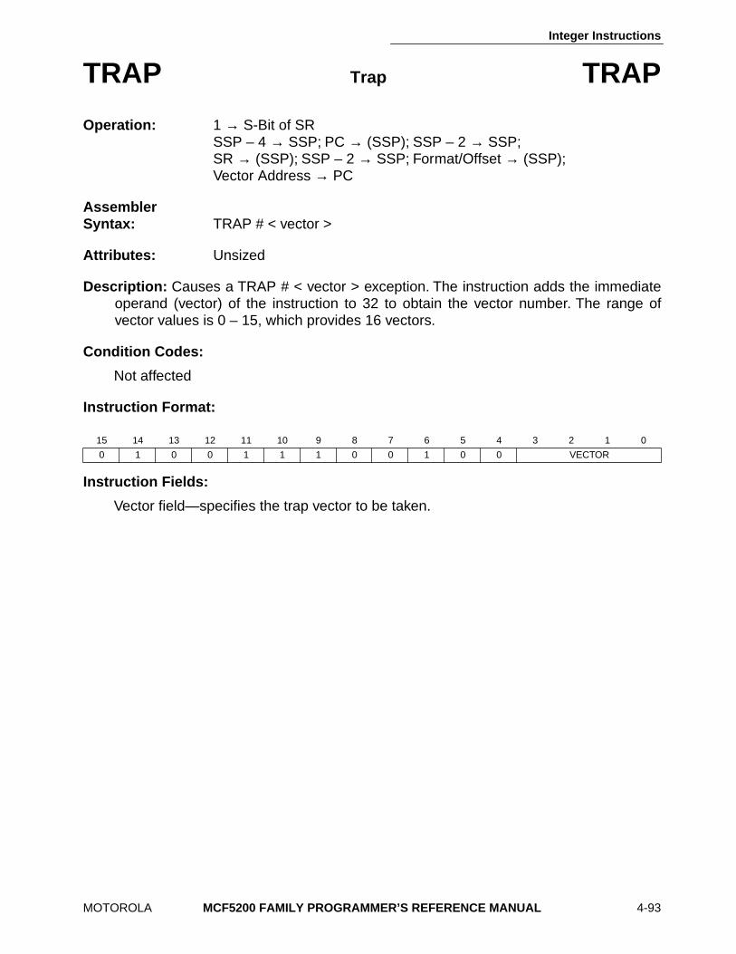
Integer Instructions
MOTOROLA MCF5200 FAMILY PROGRAMMER’S REFERENCE MANUAL 4-93
TRAP Trap TRAP
Operation: 1 → S-Bit of SR SSP – 4 → SSP; PC → (SSP); SSP – 2 → SSP; SR → (SSP); SSP – 2 → SSP; Format/Offset → (SSP); Vector Address → PC
Assembler Syntax: TRAP # < vector >
Attributes: Unsized
Description: Causes a TRAP # < vector > exception. The instruction adds the immediateoperand (vector) of the instruction to 32 to obtain the vector number. The range ofvector values is 0 – 15, which provides 16 vectors.
Condition Codes:
Not affected
Instruction Format:
Instruction Fields:
Vector field—specifies the trap vector to be taken.
15 14 13 12 11 10 9 8 7 6 5 4 3 2 1 0
0 1 0 0 1 1 1 0 0 1 0 0 VECTOR

Integer Instructions
4-94 MCF5200 FAMILY PROGRAMMER’S REFERENCE MANUAL MOTOROLA
TRAPF Trapf TRAPF
Operation: No operation
Assembler Syntax: TRAPF
TRAPF.W #<data>TRAPF.L #<data>
Attributes: Unsized or Size = Word or Long
Description: This instruction performs no operation. It can be used to occupy 16, 32, or 48bits in instruction space.
Condition Codes:
Not affected
Instruction Format:
Instruction Fields:
Vector field—specifies the trap vector to be taken.
OPMODE fields:010—instruction word without any additional extensions011—instruction word followed by one extension word100—instruction word followed by two extension words
15 14 13 12 11 10 9 8 7 6 5 4 3 2 1 0
0 1 0 1 0 0 0 1 1 1 1 1 1 OPMODE
OPTIONAL IMMEDIATE WORD
OPTIONAL IMMEDIATE WORD

Integer Instructions
MOTOROLA MCF5200 FAMILY PROGRAMMER’S REFERENCE MANUAL 4-95
TST Test an Operand TST
Operation: Destination Tested → Condition Codes
Assembler Syntax: TST < ea >
Attributes: Size = Byte, Word, Long
Description: Compares the operand with zero and sets the condition codes according tothe results of the test. The size of the operation is specified as byte, word, or long word.
Condition Codes:
X — not affected N — set if the operand is negative; cleared otherwise Z — det if the operand is zero; cleared otherwise V — always clearedC — always cleared
Instruction Format:
X N Z V C — ∗ ∗ 0 0
15 14 13 12 11 10 9 8 7 6 5 4 3 2 1 0
0 1 0 0 1 0 1 0 SIZEEFFECTIVE ADDRESS
MODE REGISTER

Integer Instructions
4-96 MCF5200 FAMILY PROGRAMMER’S REFERENCE MANUAL MOTOROLA
TST Test an Operand TST
Instruction Fields:
Size field—specifies the size of the operation: 00 — byte operation 01 — word operation 10 — long word operation
Effective Address field—specifies the addressing mode for the destination operand aslisted in the following table:
Addressing Mode Mode Register Addressing Mode Mode Register
Dn 000 reg. number:Dn (xxx).W 111 000
An 001 reg. number:An (xxx).L 111 001
(An) 010 reg. number:An #<data> 111 100
(An) + 011 reg. number:An
– (An) 100 reg. number:An
(d16,An) 101 reg. number:An (d16,PC) 111 010
(d8,An,Xn) 110 reg. number:An (d8,PC,Xn) 111 011

Integer Instructions
MOTOROLA MCF5200 FAMILY PROGRAMMER’S REFERENCE MANUAL 4-97
UNLK Unlink UNLK
Operation: An → SP; (SP) → An; SP + 4 → SP
Assembler Syntax: UNLK An
Attributes: Unsized
Description: Loads the stack pointer from the specified address register, then loads theaddress register with the long word pulled from the top of the stack.
Condition Codes:
Not affected
Instruction Format:
Instruction Field:
Register field—specifies the address register for the instruction.
15 14 13 12 11 10 9 8 7 6 5 4 3 2 1 0
0 1 0 0 1 1 1 0 0 1 0 1 1 REGISTER

Integer Instructions
4-98 MCF5200 FAMILY PROGRAMMER’S REFERENCE MANUAL MOTOROLA

Integer Instructions
MOTOROLA MCF5200 FAMILY PROGRAMMER’S REFERENCE MANUAL 4-99

Integer Instructions
4-100 MCF5200 FAMILY PROGRAMMER’S REFERENCE MANUAL MOTOROLA

MOTOROLA
MCF5200 FAMILY PROGRAMMER’S REFERENCE MANUAL
5-1
SECTION 5SUPERVISOR (PRIVILEGED) INSTRUCTIONS
This section contains information about the supervisor (privileged) instructions for theColdFire Family. Each instruction is described in detail with the instruction descriptionsarranged in alphabetical order by instruction mnemonic.
The supervisor instruction set has complete access to the user mode instructions in additionto those listed in Table 5-1.
The MOVEC instruction providess access to the various control registers dealing withsystem-level functions. This includes all the configuration registers defining the addressspace as well as a single module base address register (MBAR) that provides thespecification for the memory-mapped module configuration and control registers. Thecontrol register address, contained in bits [11:0] of the first extension word of the instruction,is defined below.
Table 5-1. Supervisor Mode Instruction Summary
Opcode Supported Operand Sizes Addressing Modes
HALT UnsizedMOVE from SR .W Dn
MOVE to SR .WDn, SR
#<data>, SRMOVEC .L Rn, Rc
RTE UnsizedSTOP Unsized #<data>
WDEBUG .L <ea>WDATA .B, .W, .L <ea>PULSE Unsized

Supervisor (Privileged) Instructions
5-2
MCF5200 FAMILY PROGRAMMER’S REFERENCE MANUAL
MOTOROLA
Note that the actual control registers in a given design are dependent of the on-chip memoryand module configurations. In addition, a ColdFire processor only supports write access toall the control registers accessed by the MOVEC instruction.
Table 5-2. CPU Space Map
Rc[11:0]
1
Register Definition
$002
Cache Control Register (CACR)
$003
MMU Translation Control Register (TCR)
$004
Access Control Unit 2 (ACR2)
$005
Access Control Unit 3 (ACR3)
$006
Access Control Unit 0 (ACR0)
$007
Access Control Unit 1 (ACR1)
$08x
2
Write the processor core address and data registers
2
$18x
2
Read the processor core address and data registers
$801
Vector Base Register (VBR)
$80E
2
Status Register (SR)
2
$C00
ROM Base Address Register (ROMBAR)
$C04
RAM Base Address Register 0 (RAMBAR0)
$C05
RAM Base Address Register 1 (RAMBAR1)
$C0F
Module Base Åddress Register (MBAR)
1
Any other code produces undefined results and should not be performed.
2
Not accessible via MOVEC; only through the Debug interface, if implemented.

Supervisor (Privileged) Instructions
MOTOROLA
MCF5200 FAMILY PROGRAMMER’S REFERENCE MANUAL
5-3
HALT
Halt the CPU (Privileged)
HALT
Operation:
If Supervisor State Then Source Halt the Processor Core
Else TRAP
Assembler Syntax:
HALT
Attributes:
Unsized
Description:
The processor core is synchronized (meaning all previous instructions and buscycles are completed), and then halts operation. The processor’s halt status is signaledon the processor status output pins. If a ‘‘go’’ debug command is received, theprocessor resumes execution at the next instruction.
Condition Codes:
Not affected
Instruction Format:
15 14 13 12 11 10 9 8 7 6 5 4 3 2 1 0
0 1 0 0 1 0 1 0 1 1 0 0 1 0 0 0

Supervisor (Privileged) Instructions
5-4
MCF5200 FAMILY PROGRAMMER’S REFERENCE MANUAL
MOTOROLA
PULSE
Generate a Unique Processor Status
PULSE
Operation:
Generate a Unique Processor Status Encoding
Assembler Syntax:
PULSE
Attributes:
Unsized
Description:
This instruction does not perform any explicit operation except for thegeneration of a unique encoding of the processor status output pins (PST = $4). Thisencoding is asserted by one processor clock cycle and is useful in providing a triggerto external logic during debug, performance characterization, etc.
Condition Codes:
Not affected
Instruction Format:
15 14 13 12 11 10 9 8 7 6 5 4 3 2 1 0
0 1 0 0 1 0 1 0 1 1 0 0 1 1 0 0

Supervisor (Privileged) Instructions
MOTOROLA
MCF5200 FAMILY PROGRAMMER’S REFERENCE MANUAL
5-5
WDDATA
Write to Debug Data
WDDATA
Operation:
Source --> DDATA Signal Pins
Assembler Syntax:
WDDATA <ea>
Attributes:
Size = Byte, Word, Long Word
Description:
This instruction fetches the operand defined by the effective address andcaptures the data in the ColdFire debug module for display on the DDATA output pins.The size of the operand determines the number of nibbles displayed on the DDATAoutput pins. The value of the debug module configuration/status register (CSR) doesnot affect the operation of this instruction.
The execution of this instruction generates a processor status encoding matching thePULSE instruction before the referenced operand is displayed on the DDATA outputs.
Condition Codes:
Not affected
Instruction Format
:
Instruction Fields:
Size field—specifies the size of the operand data:00—byte operation01—word operation10—long operation
Effective Address field—determines the addressing mode for the operand to be writtento the DDATA signal pins; use only those memory alterable addressing modes listedin the following table:
15 14 13 12 11 10 9 8 7 6 5 4 3 2 1 0
1 1 1 1 0 1 0 0 SIZEEFFECTIVE ADDRESS
MODE REGISTER
Addressing Mode Mode Register Addressing Mode Mode Register
Dn — — (xxx).W 111 000
An — — (xxx).L 111 001
(An) 010 reg. number: An #<data> — —
(An) + 011 reg. number: An
-(An) 101 reg. number: An
(d
16
, An) 101 reg. number: An (d
16
, PC) — —
(d
8
, An, Xn) 110 reg. number: An (d
8
, PC, Xn) — —

Supervisor (Privileged) Instructions
5-6
MCF5200 FAMILY PROGRAMMER’S REFERENCE MANUAL
MOTOROLA
WDEBUG
Write Debug Control Register
WDEBUG
Operation:
If Supervisor State
Then Addressed Debug Write Control Register Command ExecutedElse TRAP
Assembler Syntax:
WDEBUG <ea>
Attributes:
Size = Long
Description:
This instruction does two things. First, it fetches two consecutive long wordsfrom the memory location defined by the effective address. Second, it sends theoperands to the ColdFire debug module for execution as an instruction to write one ofthe debug control registers (DRc). The memory location defined by the effectiveaddress must be on a long word address or the behavior of the operation is undefined.The debug command must be organized in memory as follows:
where: (1) the first 16 bits define the ‘‘write debug register’’ command to the debugmodule, (2) the low-order 4 bits (DRc) define the specific control register being written,(3) the 32-bit operand to be written is defined as Data[31:0], and (4) the lower 16 bitsof the second long word are unused.
Condition Codes:
Not affected
Instruction Format
:
Instruction Fields:
Effective Address field—determines the addressing mode for debug command locationin memory.
15 14 13 12 11 10 9 8 7 6 5 4 3 2 1 0
0 0 1 0 1 1 0 0 1 0 0 0 DRc
Data[31:16]
Data[15:0]
Unused
15 14 13 12 11 10 9 8 7 6 5 4 3 2 1 0
1 1 1 1 1 0 1 1 1 1EFFECTIVE ADDRESS
MODE REGISTER
0 0 0 0 0 0 0 0 0 0 0 0 0 0 1 1
Addressing Mode Mode Register Addressing Mode Mode Register
Dn (xxx).W
An (xxx).L
(An) 010 reg. number: An #<data>
(An) + — —
- (An) — —
(d
16
, An) 101 reg. number: An (d
16
, PC)
(d
8
, An, Xn) — — (d
8
, PC, Xn)

Supervisor (Privileged) Instructions
MOTOROLA
MCF5200 FAMILY PROGRAMMER’S REFERENCE MANUAL
5-7
MOVE MOVE from SR
Move from the Status Register
from SR
Operation:
If Supervisor State Then SR
→
DestinationElse TRAP
Assembler Syntax:
MOVE SR, Dn
Attributes:
Size = (Word)
Description:
Moves the data in the status register to the destination location. Thedestination is word length. Unimplemented bits are read as zeros.
Condition Codes:
Not affected
Instruction Format:
Register field—specifies destination data register.
15 14 13 12 11 10 9 8 7 6 5 4 3 2 1 0
0 1 0 0 0 0 0 0 1 1 0 0 0 REGISTER

Supervisor (Privileged) Instructions
5-8
MCF5200 FAMILY PROGRAMMER’S REFERENCE MANUAL
MOTOROLA
MOVE MOVE to SR
Move to the Status Register
to SR
Operation:
If Supervisor State Then Source → SR
Else TRAP
Assembler Syntax: MOVE < ea >, SR
Attributes: Size = Word
Description: Moves the data in the source operand to the status register. The sourceoperand is a word, and all implemented bits of the status register are affected.
Condition Codes: Set according to the source operand
Instruction Format:
15 14 13 12 11 10 9 8 7 6 5 4 3 2 1 0
0 1 0 0 0 1 1 0 1 1EFFECTIVE ADDRESS
MODE REGISTER

Supervisor (Privileged) Instructions
MOTOROLA MCF5200 FAMILY PROGRAMMER’S REFERENCE MANUAL 5-9
MOVE MOVE to SR Move to the Status Register to SR
Instruction Field:
Effective Address field—specifies the location of the source operand; use only thosedata addressing modes listed in the following table:
Addressing Mode Mode Register Addressing Mode Mode Register
Dn 000 reg. number:Dn (xxx).W — —
An — — (xxx).L — —
(An) — — # < data > 111 100
(An) + — —
—(An) — —
(d16,An) — — (d16,PC) — —
(d8,An,Xn) — — (d8,PC,Xn) — —

Supervisor (Privileged) Instructions
5-10 MCF5200 FAMILY PROGRAMMER’S REFERENCE MANUAL MOTOROLA
MOVEC Move Control Register MOVEC
Operation: If Supervisor State Then Rn → Rc
Else TRAP
Assembler Syntax: MOVEC Rn,Rc
Attributes: Size = (Long)
Description: Moves the contents of the general register to the specified control register.Thisis always a 32-bit transfer even though the control register may be implemented withfewer bits.
Condition Codes: Not affected
Instruction Format:
Instruction Fields:
A/D field—specifies the type of general register: 0—data register 1—address register
Actual control registers in a given design can vary. Only the VBR exits in all ColdFiredesigns. Access to undefined control register space yields undefined results and must notbe attempted. Access to unimplemented, but defined, control registers generally results ina virtual no-operation. The exception to this is the MBAR register. Access to anunimplemented MBAR may result in a system hang or bus error, depending on theimplementation.
15 14 13 12 11 10 9 8 7 6 5 4 3 2 1 0
0 1 0 0 1 1 1 0 0 1 1 1 1 0 1 dr
A/D REGISTER CONTROL REGISTER
Supervisor (Privileged) Instructions
MOTOROLA MCF5200 FAMILY PROGRAMMER’S REFERENCE MANUAL 5-11
MOVEC Move Control Register MOVEC
Register field—specifies the register number.
Control Register field—specifies the control register.
Table 4-1. CPU Space MapRc[11:0] Register Definition
$002 Cache Control Register (CACR)$003 MMU Translation Control Register (TCR)$004 Access Control Unit 2 (ACR2)$005 Access Control Unit 3 (ACR3)$006 Access Control Unit 0 (ACR0)$007 Access Control Unit 1 (ACR1)$801 Vector Base Register (VBR)$C00 ROM Base Address Register (ROMBAR)$C04 RAM Base Address Register 0 (RAMBAR0)$C05 RAM Base Address Register 1 (RAMBAR1)$COF Module Base Address Register (MBAR)

Supervisor (Privileged) Instructions
5-12 MCF5200 FAMILY PROGRAMMER’S REFERENCE MANUAL MOTOROLA
RTE Return from Exception RTE
Operation: 2 (SP) → SR; 4 (SP) → PC; SP + 8→ SP Adjust stack according to format
Assembler Syntax: RTE
Attributes: Unsized
Description: Loads the processor state information stored in the exception stack framelocated at the top of the stack into the processor. The instruction examines the stackformat field in the format/offset word to determine how much information must berestored.
Condition Codes: Set according to the condition code bits in the status register valuerestored from the stack.
Instruction Format:
15 14 13 12 11 10 9 8 7 6 5 4 3 2 1 0
0 1 0 0 1 1 1 0 0 1 1 1 0 0 1 1

Supervisor (Privileged) Instructions
MOTOROLA MCF5200 FAMILY PROGRAMMER’S REFERENCE MANUAL 5-13
STOP Load Status Register and Stop STOP
Operation: If Supervisor State Then Immediate Data → SR; STOP
Else TRAP
Assembler Syntax: STOP # < data >
Attributes: Unsized
Description: (1) Moves the immediate operand into the status register (both user andsupervisor portions), (2) advances the program counter to point to the next instruction,and (3) stops the fetching and executing of instructions. A trace, interrupt, or resetexception causes the processor to resume instruction execution. A trace exceptionoccurs if instruction tracing is enabled (T0 = 1) when the STOP instruction beginsexecution. If an interrupt request is asserted with a priority higher than the priority levelset by the new status register value, an interrupt exception occurs; otherwise, theinterrupt request is ignored. External reset always initiates reset exception processing.In the ColdFire processors, the STOP command places the processor in a low-powerstate.
Condition Codes: Set according to the immediate operand.
Instruction Format:
Instruction Fields:
Immediate field—specifies the data to be loaded into the status register.
15 14 13 12 11 10 9 8 7 6 5 4 3 2 1 0
0 1 0 0 1 1 1 0 0 1 1 1 0 0 1 0
IMMEDIATE DATA

Supervisor (Privileged) Instructions
5-14 MCF5200 FAMILY PROGRAMMER’S REFERENCE MANUAL MOTOROLA

MOTOROLA
MCF5200 FAMILY PROGRAMMER’S REFERENCE MANUAL
6-1
SECTION 6INSTRUCTION FORMAT SUMMARY
This section contains a listing of the ColdFire family instructions in binary format.
6.1 INSTRUCTION FORMAT
The following paragraphs present a summary of the binary encoding fields.
6.1.1 Effective Address Field
This field specifies which addressing mode is to be used. Some operations allow hardware-enforced restrictions on the available addressing modes.
6.1.2 Shift Instruction
The following paragraphs define the fields used with the shift instructions.
6.1.2.1 Count Register Field.
If i/r = 0, this field contains the shift count of 1 – 8 (a zerospecifies 8). If i/r = 1, this field specifies a data register that contains the shift count. Thefollowing shift fields are encoded as follows:
dr field: 0— shift right 1— shift left
i/r field: 0 — immediate shift count 1 — register shift count
6.1.2.2 Register Field.
This field specifies a data register to be shifted.

Instruction Format Summary
6-2
MCF5200 FAMILY PROGRAMMER’S REFERENCE MANUAL
MOTOROLA
6.1.3 Size Field
This field specifies the size of the operation and is encoded as follows:
00 — byte operation 01 — word operation 10 — long operation
6.1.4 Opmode Field
Refer to the applicable instruction descriptions for the encoding of this field.
6.1.5 Address/Data Field
This field specifies the type of general register and is encoded as follows:
0 — data register 1 — address register
6.2 OPERATION CODE MAP
Table 6-1 lists the encoding for bits 15 – 12 and the operation performed.
Table 6-1. Operation Code Map
Bits 15 – 12 Operation
0000 Bit Manipulation/MOVEP/Immed iate
0001 Move Byte
0010 Move Long
0011 Move Word
0100 Miscellaneous
0101 ADDQ/SUBQ/Scc
0110 Bcc/BSR/BRA
0111 MOVEQ
1000 OR
1001 SUB/SUBX
1010 (Unassigned, Reserved)
1011 CMP/EOR
1100 AND/MUL /EXG
1101 ADD/ADDX
1110 Shift/Bit Field
1111 Unassigned reserved

Instruction Format Summary
MOTOROLA
MCF5200 FAMILY PROGRAMMER’S REFERENCE MANUAL
6-3
1. ORI
2. ANDI
3. SUBI
4. ADDI
5. EORI
6. CMPI
7. BTST
BIT NUMBER STATIC, SPECIFIED AS IMMEDIATE DATA
15 14 13 12 11 10 9 8 7 6 5 4 3 2 1 0
0 0 0 0 0 0 0 0 1 0 0 0 0 REGISTER
UPPER WORD OF IMMEDIATE DATA
LOWER WORD OF IMMEDIATE DATA
15 14 13 12 11 10 9 8 7 6 5 4 3 2 1 0
0 0 0 0 0 0 0 0 1 0 0 0 0 REGISTER
UPPER WORD OF IMMEDIATE DATA
LOWER WORD OF IMMEDIATE DATA
15 14 13 12 11 10 9 8 7 6 5 4 3 2 1 0
0 0 0 0 0 1 0 0 1 0 0 0 0 REGISTER
UPPER WORD OF IMMEDIATE DATA
LOWER WORD OF IMMEDIATE DATA
15 14 13 12 11 10 9 8 7 6 5 4 3 2 1 0
0 0 0 0 0 1 1 0 1 0 0 0 0 REGISTER
UPPER WORD OF IMMEDIATE DATA
LOWER WORD OF IMMEDIATE DATA
15 14 13 12 11 10 9 8 7 6 5 4 3 2 1 0
0 0 0 0 1 0 1 0 1 0 0 0 0 REGISTER
UPPER WORD OF IMMEDIATE DATA
LOWER WORD OF IMMEDIATE DATA
15 14 13 12 11 10 9 8 7 6 5 4 3 2 1 0
0 0 0 0 1 1 0 0 1 0 0 0 0 REGISTER
UPPER WORD OF IMMEDIATE DATA
LOWER WORD OF IMMEDIATE DATA
15 14 13 12 11 10 9 8 7 6 5 4 3 2 1 0
0 0 0 0 1 0 0 0 0 0EFFECTIVE ADDRESS
MODE REGISTER
0 0 0 0 0 0 0 0 BIT NUMBER

Instruction Format Summary
6-4
MCF5200 FAMILY PROGRAMMER’S REFERENCE MANUAL
MOTOROLA
8. BCHG
BIT NUMBER STATIC, SPECIFIED AS IMMEDIATE DATA
9. BCLR
BIT NUMBER STATIC, SPECIFIED AS IMMEDIATE DATA
10. BSET
BIT NUMBER STATIC, SPECIFIED AS IMMEDIATE DATA
11. BTST
BIT NUMBER DYNAMIC, SPECIFIED IN A REGISTER
12. BCHG
BIT NUMBER DYNAMIC, SPECIFIED IN A REGISTER
13. BCLR
BIT NUMBER DYNAMIC, SPECIFIED IN A REGISTER
14. BSET
BIT NUMBER DYNAMIC, SPECIFIED IN A REGISTER
15 14 13 12 11 10 9 8 7 6 5 4 3 2 1 0
0 0 0 0 1 0 0 0 0 1EFFECTIVE ADDRESS
MODE REGISTER
0 0 0 0 0 0 0 0 BIT NUMBER
15 14 13 12 11 10 9 8 7 6 5 4 3 2 1 0
0 0 0 0 1 0 0 0 1 0EFFECTIVE ADDRESS
MODE REGISTER
0 0 0 0 0 0 0 0 BIT NUMBER
15 14 13 12 11 10 9 8 7 6 5 4 3 2 1 0
0 0 0 0 1 0 0 0 1 1EFFECTIVE ADDRESS
MODE REGISTER
0 0 0 0 0 0 0 BIT NUMBER
15 14 13 12 11 10 9 8 7 6 5 4 3 2 1 0
0 0 0 0 REGISTER 1 0 0EFFECTIVE ADDRESS
MODE REGISTER
15 14 13 12 11 10 9 8 7 6 5 4 3 2 1 0
0 0 0 0 REGISTER 1 0 1EFFECTIVE ADDRESS
MODE REGISTER
15 14 13 12 11 10 9 8 7 6 5 4 3 2 1 0
0 0 0 0 REGISTER 1 1 0EFFECTIVE ADDRESS
MODE REGISTER
15 14 13 12 11 10 9 8 7 6 5 4 3 2 1 0
0 0 0 0 REGISTER 1 1 1EFFECTIVE ADDRESS
MODE REGISTER
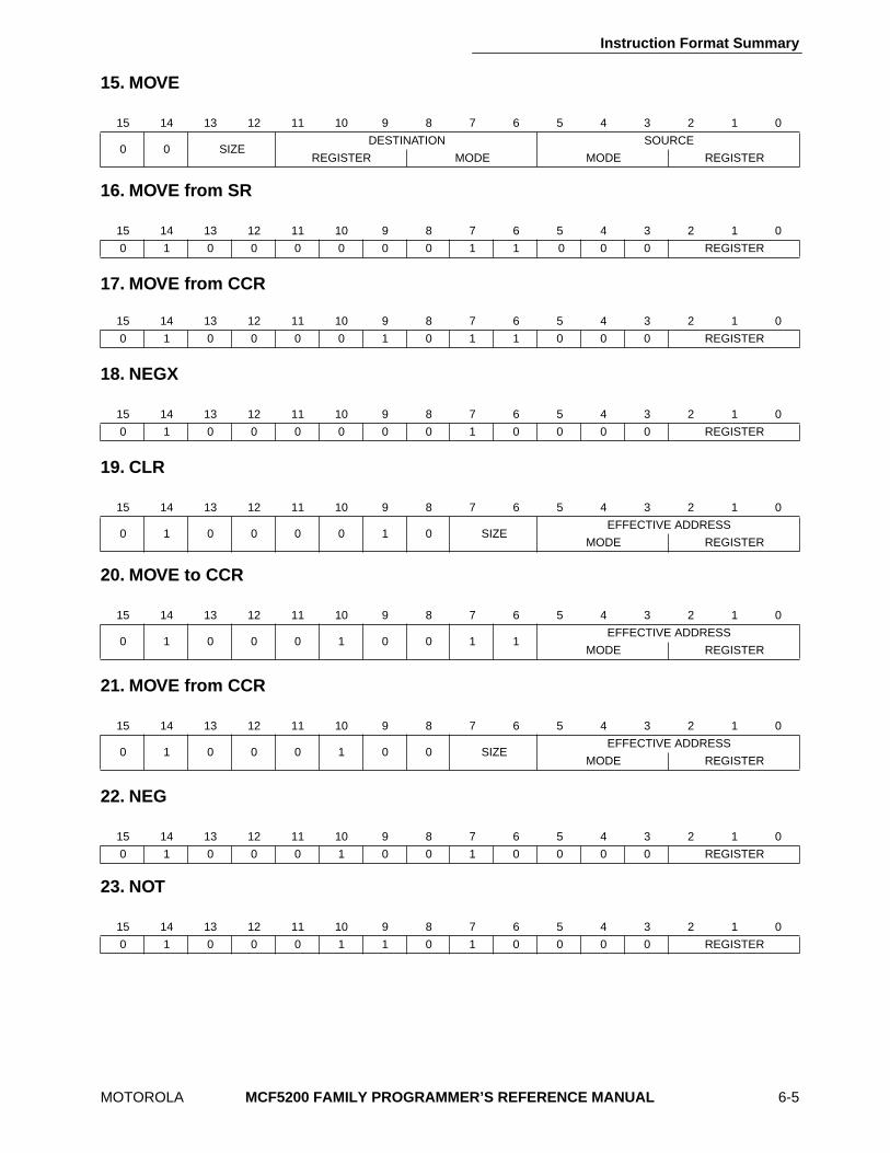
Instruction Format Summary
MOTOROLA
MCF5200 FAMILY PROGRAMMER’S REFERENCE MANUAL
6-5
15. MOVE
16. MOVE from SR
17. MOVE from CCR
18. NEGX
19. CLR
20. MOVE to CCR
21. MOVE from CCR
22. NEG
23. NOT
15 14 13 12 11 10 9 8 7 6 5 4 3 2 1 0
0 0 SIZEDESTINATION SOURCE
REGISTER MODE MODE REGISTER
15 14 13 12 11 10 9 8 7 6 5 4 3 2 1 0
0 1 0 0 0 0 0 0 1 1 0 0 0 REGISTER
15 14 13 12 11 10 9 8 7 6 5 4 3 2 1 0
0 1 0 0 0 0 1 0 1 1 0 0 0 REGISTER
15 14 13 12 11 10 9 8 7 6 5 4 3 2 1 0
0 1 0 0 0 0 0 0 1 0 0 0 0 REGISTER
15 14 13 12 11 10 9 8 7 6 5 4 3 2 1 0
0 1 0 0 0 0 1 0 SIZEEFFECTIVE ADDRESS
MODE REGISTER
15 14 13 12 11 10 9 8 7 6 5 4 3 2 1 0
0 1 0 0 0 1 0 0 1 1EFFECTIVE ADDRESS
MODE REGISTER
15 14 13 12 11 10 9 8 7 6 5 4 3 2 1 0
0 1 0 0 0 1 0 0 SIZEEFFECTIVE ADDRESS
MODE REGISTER
15 14 13 12 11 10 9 8 7 6 5 4 3 2 1 0
0 1 0 0 0 1 0 0 1 0 0 0 0 REGISTER
15 14 13 12 11 10 9 8 7 6 5 4 3 2 1 0
0 1 0 0 0 1 1 0 1 0 0 0 0 REGISTER

Instruction Format Summary
6-6
MCF5200 FAMILY PROGRAMMER’S REFERENCE MANUAL
MOTOROLA
24. MOVE to SR
25. EXT, EXTB
26. SWAP
27. PEA
28. TST
29. HALT
30. PULSE
31. MULU
WORD
LONG
15 14 13 12 11 10 9 8 7 6 5 4 3 2 1 0
0 1 0 0 0 1 1 0 1 1EFFECTIVE ADDRESS
MODE REGISTER
15 14 13 12 11 10 9 8 7 6 5 4 3 2 1 0
0 1 0 0 1 0 0 OPMODE 0 0 0 REGISTER
15 14 13 12 11 10 9 8 7 6 5 4 3 2 1 0
0 1 0 0 1 0 0 0 0 1 0 0 0 REGISTER
15 14 13 12 11 10 9 8 7 6 5 4 3 2 1 0
0 1 0 0 1 0 0 0 0 1EFFECTIVE ADDRESS
MODE REGISTER
15 14 13 12 11 10 9 8 7 6 5 4 3 2 1 0
0 1 0 0 1 0 1 0 SIZEEFFECTIVE ADDRESS
MODE REGISTER
15 14 13 12 11 10 9 8 7 6 5 4 3 2 1 0
0 1 0 0 1 0 1 0 1 1 0 0 1 0 0 0
15 14 13 12 11 10 9 8 7 6 5 4 3 2 1 0
0 1 0 0 1 0 1 1 1 1 0 0 1 1 0 0
15 14 13 12 11 10 9 8 7 6 5 4 3 2 1 0
1 1 0 0 REGISTER 0 1 1EFFECTIVE ADDRESS
MODE REGISTER
15 14 13 12 11 10 9 8 7 6 5 4 3 2 1 0
0 1 0 0 1 1 0 0 0 0EFFECTIVE ADDRESS
MODE REGISTER
0 REGISTER DI 0 0 0 0 0 0 0 0 0 0 0 0

Instruction Format Summary
MOTOROLA
MCF5200 FAMILY PROGRAMMER’S REFERENCE MANUAL
6-7
32. MULS
WORD
LONG
33. TRAP
34. LINK
WORD
35. NOP
36. STOP
37. RTE
38. RTS
39. MOVEC
15 14 13 12 11 10 9 8 7 6 5 4 3 2 1 0
1 1 0 0 REGISTER 1 1 1EFFECTIVE ADDRESS
MODE REGISTER
15 14 13 12 11 10 9 8 7 6 5 4 3 2 1 0
0 1 0 0 1 1 0 0 0 0EFFECTIVE ADDRESS
MODE REGISTER
0 REGISTER DI 1 0 0 0 0 0 0 0 0 0 0 0
15 14 13 12 11 10 9 8 7 6 5 4 3 2 1 0
0 1 0 0 1 1 1 0 0 1 0 0 VECTOR
15 14 13 12 11 10 9 8 7 6 5 4 3 2 1 0
0 1 0 0 1 1 1 0 0 1 0 1 0 REGISTER
WORD DISPLACEMENT
15 14 13 12 11 10 9 8 7 6 5 4 3 2 1 0
0 1 0 0 1 1 1 0 0 1 1 1 0 0 0 1
15 14 13 12 11 10 9 8 7 6 5 4 3 2 1 0
0 1 0 0 1 1 1 0 0 1 1 1 0 0 1 0
IMMEDIATE DATA
15 14 13 12 11 10 9 8 7 6 5 4 3 2 1 0
0 1 0 0 1 1 1 0 0 1 1 1 0 0 1 1
15 14 13 12 11 10 9 8 7 6 5 4 3 2 1 0
0 1 0 0 1 1 1 0 0 1 1 1 0 1 0 1
15 14 13 12 11 10 9 8 7 6 5 4 3 2 1 0
0 1 0 0 1 1 1 0 0 1 1 1 1 0 1 dr
A/D REGISTER CONTROL REGISTER

Instruction Format Summary
6-8
MCF5200 FAMILY PROGRAMMER’S REFERENCE MANUAL
MOTOROLA
40. JSR
41. JMP
42. MOVEM
43. LEA
44. ADDQ
45. SUBQ
46. Scc
47. BRA
15 14 13 12 11 10 9 8 7 6 5 4 3 2 1 0
0 1 0 0 1 1 1 0 1 0EFFECTIVE ADDRESS
MODE REGISTER
15 14 13 12 11 10 9 8 7 6 5 4 3 2 1 0
0 1 0 0 1 1 1 0 1 1EFFECTIVE ADDRESS
MODE REGISTER
15 14 13 12 11 10 9 8 7 6 5 4 3 2 1 0
0 1 0 0 1 dr 0 0 1 1EFFECTIVE ADDRESS
MODE REGISTER
REGISTER LIST MASK
15 14 13 12 11 10 9 8 7 6 5 4 3 2 1 0
0 1 0 0 REGISTER 1 1 1EFFECTIVE ADDRESS
MODE REGISTER
15 14 13 12 11 10 9 8 7 6 5 4 3 2 1 0
0 1 0 1 DATA 0 1 0EFFECTIVE ADDRESS
MODE REGISTER
15 14 13 12 11 10 9 8 7 6 5 4 3 2 1 0
0 1 0 1 DATA 1 1 0EFFECTIVE ADDRESS
MODE REGISTER
15 14 13 12 11 10 9 8 7 6 5 4 3 2 1 0
0 1 0 1 CONDITION 1 1EFFECTIVE ADDRESS
MODE REGISTER
15 14 13 12 11 10 9 8 7 6 5 4 3 2 1 0
0 1 1 0 0 0 0 0 8-BIT DISPLACEMENT
16-BIT DISPLACEMENT IF 8-BIT DISPLACEMENT = $00

Instruction Format Summary
MOTOROLA
MCF5200 FAMILY PROGRAMMER’S REFERENCE MANUAL
6-9
48. BSR
49. Bcc
50. MOVEQ
51. OR
52. SUBX
53. SUB
54. SUBA
55. CMP
56. CMPA
15 14 13 12 11 10 9 8 7 6 5 4 3 2 1 0
0 1 1 0 0 0 0 1 8-BIT DISPLACEMENT
16-BIT DISPLACEMENT IF 8-BIT DISPLACEMENT = $00
15 14 13 12 11 10 9 8 7 6 5 4 3 2 1 0
0 1 1 0 CONDITION 8-BIT DISPLACEMENT
16-BIT DISPLACEMENT IF 8-BIT DISPLACEMENT = $00
15 14 13 12 11 10 9 8 7 6 5 4 3 2 1 0
0 1 1 1 REGISTER 0 DATA
15 14 13 12 11 10 9 8 7 6 5 4 3 2 1 0
1 0 0 0 REGISTER OPMODEEFFECTIVE ADDRESS
MODE REGISTER
15 14 13 12 11 10 9 8 7 6 5 4 3 2 1 0
1 0 0 1 REGISTER Dy 1 1 0 0 0 0 REGISTER Dx
15 14 13 12 11 10 9 8 7 6 5 4 3 2 1 0
1 0 0 1 REGISTER OPMODEEFFECTIVE ADDRESS
MODE REGISTER
15 14 13 12 11 10 9 8 7 6 5 4 3 2 1 0
1 0 0 1 REGISTER 1 1 1EFFECTIVE ADDRESS
MODE REGISTER
15 14 13 12 11 10 9 8 7 6 5 4 3 2 1 0
1 0 1 1 REGISTER 0 1 0EFFECTIVE ADDRESS
MODE REGISTER
15 14 13 12 11 10 9 8 7 6 5 4 3 2 1 0
1 0 1 1 REGISTER 1 1 1EFFECTIVE ADDRESS
MODE REGISTER

Instruction Format Summary
6-10
MCF5200 FAMILY PROGRAMMER’S REFERENCE MANUAL
MOTOROLA
57. EOR
58. MULU
WORD
59. MULS
WORD
60. AND
61. ADDX
62. ADDA
63. ADD
64. ASL, ASR
REGISTER SHIFT
65. LSL, LSR
REGISTER SHIFT
15 14 13 12 11 10 9 8 7 6 5 4 3 2 1 0
1 0 1 1 REGISTER 1 1 0EFFECTIVE ADDRESS
MODE REGISTER
15 14 13 12 11 10 9 8 7 6 5 4 3 2 1 0
1 1 0 0 REGISTER 0 1 1EFFECTIVE ADDRESS
MODE REGISTER
15 14 13 12 11 10 9 8 7 6 5 4 3 2 1 0
1 1 0 0 REGISTER 1 1 1EFFECTIVE ADDRESS
MODE REGISTER
15 14 13 12 11 10 9 8 7 6 5 4 3 2 1 0
1 1 0 0 REGISTER OPMODEEFFECTIVE ADDRESS
MODE REGISTER
15 14 13 12 11 10 9 8 7 6 5 4 3 2 1 0
1 1 0 1 REGISTER Dy 1 1 0 0 0 0 REGISTER Dy
15 14 13 12 11 10 9 8 7 6 5 4 3 2 1 0
1 1 0 1 REGISTER 1 1 1EFFECTIVE ADDRESS
MODE REGISTER
15 14 13 12 11 10 9 8 7 6 5 4 3 2 1 0
1 1 0 1 REGISTER OPMODEEFFECTIVE ADDRESS
MODE REGISTER
15 14 13 12 11 10 9 8 7 6 5 4 3 2 1 0
1 1 1 0COUNT/
REGISTERdr 1 0 i/r 0 0 REGISTER
15 14 13 12 11 10 9 8 7 6 5 4 3 2 1 0
1 1 1 0COUNT/
REGISTERdr 1 0 i/r 0 1 REGISTER

Instruction Format Summary
MOTOROLA
MCF5200 FAMILY PROGRAMMER’S REFERENCE MANUAL
6-11
66. WDDATA
67. WDEBUG
15 14 13 12 11 10 9 8 7 6 5 4 3 2 1 0
1 1 1 1 1 0 1 1 SIZEEFFECTIVE ADDRESS
MODE REGISTER
15 14 13 12 11 10 9 8 7 6 5 4 3 2 1 0
1 1 1 1 1 0 1 1 1 1EFFECTIVE ADDRESS
MODE REGISTER
0 0 0 0 0 0 0 0 0 0 0 0 0 0 1 1

Instruction Format Summary
6-12
MCF5200 FAMILY PROGRAMMER’S REFERENCE MANUAL
MOTOROLA
MOTOROLA
MCF5200 FAMILY PROGRAMMER’S REFERENCE MANUAL
7-1
SECTION 7 EXCEPTION PROCESSING
Exception processing is the activity performed by the processor in preparing to execute aspecial routine for any condition that causes an exception. Exception processing does notinclude execution of the routine itself.
This section describes the processing for each type of integer unit exception, exception pri-orities, the return from an exception, and bus fault recovery. Also described are the formatsof the exception stack frames.
7.1 EXCEPTION PROCESSING OVERVIEW
Exception processing is the transition from the normal processing of a program to the pro-cessing required for any special internal or external condition that preempts normal process-ing. External conditions that cause exceptions are interrupts from external devices, buserrors, and resets. Internal conditions that cause exceptions are instructions, addresserrors, and tracing. In addition, some instructions such as the TRAP and RTE instructionscan generate exceptions as part of their normal execution. Illegal instructions and privilegeviolations cause exceptions as well. Exception processing uses an exception vector tableand an exception stack frame. The following paragraphs describe the vector table and ageneralized exception stack frame.
The ColdFire processor uses an instruction restart exception model but does require addi-tional software support to recover from certain types of exceptions, i.e., access and addresserrors.
Exception processing is defined as the time from the detection of the fault condition until thefirst instruction of the handler has been fetched. Figure 7-1 illustrates a general flowchart forthe steps taken by the processor during exception processing.

Exception Processing
7-2
MCF5200 FAMILY PROGRAMMER’S REFERENCE MANUAL
MOTOROLA
Figure 7-1. General Exception Processing Flowchart
First, the processor (a) makes an internal copy of the status register (SR), (b) enters super-visor mode by asserting the S-bit and (c) disables trace mode by negating the T-bit. Also,an interrupt exception forces an update of the interrupt priority mask.
Second, the processor determines the vector number of the exception. For all faults
except
interrupts, the processor performs this calculation based on the exception type. For inter-rupts, the processor performs an interrupt acknowledge (IACK) bus cycle to obtain the vec-tor number from a peripheral device. The IACK cycle is mapped to a special acknowledgeaddress space with the interrupt level encoded in the transfer modifier.
Third, the processor saves the current context by creating an exception stack frame on thesystem stack. Note the ColdFire processor supports a single stack pointer in the A7 addressregister, i.e., there is no notion of a supervisor or user stack pointer. As a result, the excep-
ENTRY
SAVE INTERNAL COPY OF SR
S --> 1T --> 0
DETERMINEVECTOR NUMBER
SAVE CONTENTS TOSTACK FRAME
OTHERWISE
CALCULATEADDRESS OF FIRST
INSTRUCTION OFEXCEPTION HANDLER
FETCH FIRSTINSTRUCTION OF
EXCEPTION HANDLER
OTHERWISE
BEGIN EXECUTIONOF EXCEPTION
HANDLER
EXIT
HALTED STATE
EXIT
(DOUBLE BUS FAULT)
BUS ERROR ORADDRESS ERROR
(DOUBLE BUS FAULT)
BUS ERROR
(SEE NOTE)
(SEE NOTE)
NOTE: THESE BLOCKS VARY FOR RESET AND INTERRUPT EXCEPTIONS.

Exception Processing
MOTOROLA
MCF5200 FAMILY PROGRAMMER’S REFERENCE MANUAL
7-3
tion stack frame is created on the top of the current system stack. The processor alwaysforces the alignment of the exception stack frame to a 0-modulo-4 address, independent ofthe stack pointer value at the time of the exception. Additionally, the processor uses a sim-plified fixed-length stack frame for all exceptions, as shown in Figure 7-2. The exception typedetermines whether the program counter placed in the exception stack frame defines thelocation of the faulting instruction (Fault) or the address of the next instruction to be executed(Next).
Fourth, the processor calculates the address of the first instruction of the exception handler.This address is generated by fetching an exception vector from the table located at the 0-modulo-1M address defined in the vector base register. For the ColdFire processor, relocat-ing the exception vector table has been limited to 0-modulo-1M addresses. The index intothe exception table is calculated as (4 x Vector_Number). Once the exception vector hasbeen fetched, the vector contents determine the address of the first instruction of the desiredhandler. After fetching this initial handler instruction, exception processing terminates andnormal instruction processing continues in the handler.
The ColdFire processor supports a 1024-byte vector table aligned on any 0-modulo-1Maddress (see Table 7-1). The table contains 256 exception vectors where the first 64 aredefined by Motorola and the remaining 192 are user-defined interrupt vectors. Externaldevices can use vectors reserved for internal purposes at the discretion of the systemdesigner. They can also supply vector numbers for some exceptions. External devices thatcannot supply vector numbers use the autovector capability, which allows the processor toautomatically generate a vector number.
Figure 7-2. Exception Stack Frame Form
FORMAT FS[3:2] VECTOR[7:0] FS[1:0] STATUS REGISTER[15:0]
PROGRAM COUNTER[31:0]
SP
+ $04
31 1615 0

Exception Processing
7-4
MCF5200 FAMILY PROGRAMMER’S REFERENCE MANUAL
MOTOROLA
The ColdFire processor optionally supports autovectored interrupts. If the hardware moduleis included in the system, it converts an asserted
AVEC
signal into the appropriate vectorfor transmission to the processor core.
The ColdFire processor inhibits sampling for interrupts during the first instruction of allexception handlers. This allows any handler to effectively disable interrupts, if desired, byraising the interrupt mask level contained in the status register.
Normally, the end of an exception handler contains an RTE instruction. When the processorexecutes the RTE instruction, it examines the stack frame on top of the stack to determineif it is a valid frame. If the processor determines that it is a valid frame, the SR and PC fieldsare loaded from the exception frame and control is passed to the specified instructionaddress.
All exception vectors are located in the supervisor address space and are accessed usingdata references. Only the initial reset vector is fixed in the processor’s memory map; onceinitialization is complete, there are no fixed assignments. Since the VBR provides the baseaddress of the exception vector table, the exception vector table can be located anywherein memory; it can even be dynamically relocated for each task that an operating system exe-cutes.
Table 7-1. Exception Vector Assignments
VectorNumber(s)
VectorOffset (Hex)
StackedProgramCounter
Assignment
0 $000 - Initial Stack Pointer1 $004 - Initial Program Counter2 $008 Fault Access Error3 $00C Fault Address Error4 $010 Fault Illegal Instruction
5-7 $014-$01C - Reserved8 $020 Fault Privilege Violation9 $024 Next Trace10 $028 Fault Unimplemented Line-A Opcode11 $02C Fault Unimplemented Line-F Opcode12 $030 Next Debug Interrupt13 $034 - Reserved14 $038 Fault Format Error15 $03C Next Uninitialized Interrupt
16-23 $040-$05C - Reserved24 $060 Next Spurious Interrupt
25-31 $064-$07C Next Level 1-7 Autovectored Interrupts32-47 $080-$0BC Next TRAP # 0-15 Instructions48-63 $0C0-$0FC - Reserved64-255 $100-$3FC Next User-Defined Interrupts
“Fault” refers to the PC of the instruction that caused the exception“Next” refers to the PC of the next instruction that follows the instruction that caused the fault.

Exception Processing
MOTOROLA
MCF5200 FAMILY PROGRAMMER’S REFERENCE MANUAL
7-5
7.2 EXCEPTION STACK FRAME DEFINITION
The first longword of the exception stack frame contains the 16-bit format/vector word (F/V) and the 16-bit status register, and the second longword contains the 32-bit programcounter address.
The 16-bit format/vector word contains 3 unique fields:
1. A 4-bit format field contained in bits[31:28] at the top of the system stack is always writ-ten by the processor with a value of {4,5,6,7} indicating a 2-longword frame format and the size of the stack pointer adjustment required to force 0-modulo-4 alignment. See Table 7-2.
2. A 4-bit fault status field, FS[3:0], contained in bits[27:26, 17:16] at the top of the system stack. This field is defined for access and address errors only, and written as zeros for all other types of exceptions (see Table 7-3).
3. The 8-bit vector number, vector[7:0], defines the exception type and is calculated by the processor for all internal faults and represents the value supplied by the peripheral in the case of an interrupt. Refer to Table 7-1.
Table 7-2. Format Field Encodings
Original A7 @ Time of Exception, bits 1:0
A7 @ 1st Instructionof Handler
Format Field
00 Original A7 - 8 0100
01 Original A7 - 9 0101
10 Original A7 - 10 0110
11 Original A7 - 11 0111
Table 7-3. Fault Status Encodings
FS[3:0] Definition
00xx Reserved
0100 Physical bus error on instruction fetch
0101 Reserved
011x Reserved
1000 Physical bus error on operand write
1001 Attempted write to write-protected space
101x Reserved
1100 Physical bus error on operand read
1101 Reserved
111x Reserved

Exception Processing
7-6
MCF5200 FAMILY PROGRAMMER’S REFERENCE MANUAL
MOTOROLA
7.3 PROCESSOR EXCEPTIONS
The following paragraphs describe the external interrupt exceptions and the different typesof exceptions generated internally by the integer unit. The following exceptions are dis-cussed:
• Access Error• Address Error
• Instruction Trap
• Illegal Instruction Exceptions
• Privilege Violation
• Trace
• Format Error
• Breakpoint Instruction
• Interrupt
• Reset
7.3.1 Access Error Exception
An access error exception in the ColdFire architecture occurs when a bus cycle terminateswith an error condition such as TEA. The exact response by the ColdFire processor to anaccess error depends on the type of bus cycle being performed.
If an instruction fetch results in an access error, the processor postpones error reportinguntil the faulted reference is needed by an instruction for execution. Thus, faults that occurduring instruction prefetches which are then followed by a change of instruction flow will notgenerate an exception. When the processor tries to execute an instruction with a faultedopword and/or extension words, the access error will be signaled and the instructionaborted. For this type of exception, the programming model has not been altered by theinstruction generating the access error.
If the access error occurs on an operand read, the processor immediately aborts the currentinstruction execution and initiates exception processing. In this situation, any address reg-ister updates due to the auto-addressing modes (e.g., (An)+, -(An)), will already have beenperformed. Thus, the programming model contains the updated An value.
The ColdFire processor uses an imprecise reporting mechanism for access errors on oper-and writes. Because the actual write cycle may be decoupled from the processor’s issuingof the operation, an access error signal appears to be decoupled from the instruction thatgenerated the write. Accordingly, the PC contained in the exception stack frame merely rep-resents the location in the program when the access error was signaled. All programmingmodel updates associated with the write instruction are completed. The NOP instruction cancollect
access errors for writes. This instruction delays its execution until all previous oper-ations (including all pending write operations) are complete. If any previous write terminateswith an access error, it is guaranteed to be reported on the NOP instruction.

Exception Processing
MOTOROLA
MCF5200 FAMILY PROGRAMMER’S REFERENCE MANUAL
7-7
When the processor encounters an access error during the exception processing sequenceof another exception, the processor enters a halted state.
7.3.2 Address Error Exception
Any attempted execution transferring control to an odd instruction address (i.e., if bit 0 of thetarget address is = 1) results in an address error exception.
The ColdFire processor default configuration supports word- and longword-sized operandreferences on 0-modulo-2 and 0-modulo-4 addresses, respectively. All other references aredefined as misaligned
accesses. Any attempt to access a misaligned operand generates anaddress-error exception, unless the optional hardware module for handling misalignment ispresent. This misalignment module converts any misaligned operand references into aseries of aligned bus cycles to access the data. The existence of the misalignment moduleis implementation-dependent and is documented in the appropriate ColdFire user’s manual.
Any attempted use of a word-sized index register (Xn.w) or a scale factor of 8 on an indexedeffective addressing mode generates an address error, as does attempted execution of afull-format indexed addressing mode.
Finally, when the processor encounters an address error during the exception processingsequence of another exception, the processor enters a halted state.
7.3.3 Trap Exception
The TRAP #n instruction always forces an exception and is useful for implementing systemcalls in user programs. Typically, passing a variable to the trap handler is done throughregisters. Otherwise, if passed through the stack, the stack frame format needs to bequeried to determine the proper offset to the passed variables on the stack.
7.3.4 Illegal Instruction Exception
Attempting to execute the
$0000
and the
$4AFC
opwords generates an illegal instructionexception. Additionally, attempting to execute any line A and most line F opcode generatestheir unique exception types, vectors 10 and 11 respectively. The ColdFire processor doesnot provide illegal instruction detection on the extension words on any instruction, including
MOVEC
.
7.3.5 Privilege Violation
Any attempt to execute a supervisor mode instruction while in user mode will generate aprivilege violation exception.
7.3.6 Trace Exception
To aid in program development, the ColdFire processor provides an instruction-by-instruc-tion tracing capability. While in trace mode (indicated by the assertion of the T-bit in the sta-tus register (SR[15] = 1)), the completion of an instruction execution signals a traceexception. This functionality allows a debugger to monitor execution of a program.

Exception Processing
7-8
MCF5200 FAMILY PROGRAMMER’S REFERENCE MANUAL
MOTOROLA
In general terms, a trace exception is an extension to the function of any traced instruction.The execution of a traced instruction is not complete until trace exception processing is com-plete. If an instruction does not complete because of an access error or address error excep-tion, trace exception processing is deferred until the suspended instruction resumesexecution. If an interrupt is pending at the completion of an instruction, trace exception pro-cessing occurs before interrupt exception processing starts. If an instruction forces anexception as part of its normal execution, the forced exception processing occurs before thetrace exception is processed.
The T-bit in the supervisor portion of the SR controls tracing. The state of the T-bit when aninstruction begins execution determines whether the instruction generates a trace exceptionafter the instruction completes.
Note that if the processor is executing in trace mode when a group 2 exception is signaled,a trace exception will not be generated. This means that for the second example, as theTRAP exception handler completes its execution and performs its RTE, the next instructionof the program sequence will be executed before the next trace exception is performed (theMC68060 will not trace immediately after the TRAP). If tracing is required immediately fol-lowing a group 2 exception, the SR contained in the exception stack frame should bechecked before returning to the next instruction. If the stacked SR indicates that the proces-sor was executing in trace mode, the trace handler should be executed to account for theinstruction that initiated the exception.
7.3.7 Debug Interrupt
This special type of program interrupt is reserved for use with the Debug module. Thisexception is generated in response to a hardware breakpoint register trigger. The processordoes not generate an IACK cycle, but rather calculates the vector number internally (vector$030).
7.3.8 RTE and Format Error Exceptions
When an RTE instruction is executed, the processor first examines the 4-bit format field tovalidate the frame type. For the ColdFire processor, any attempted execution of an RTEwhere the format is not equal to {4,5,6,7} generates a format error. The exception stackframe for the format error is created without disturbing the original RTE frame and thestacked PC pointing to the RTE instruction.
The format value corresponds to the required system stack pointer adjustment to return itto the value at the time of the exception. This mechanism essentially negates the self-align-ing operation to restore the stack pointer to its original value.
The selection of the format value provides some limited debug support for porting code from68000 applications. On 680x0 family processors, the status register (SR) was located at thetop of the stack. On those processors, bit[30] of the longword addressed by the system stackpointer is typically zero. Thus, an attempted RTE using this “old” format generates a formaterror on the ColdFire processor.

Exception Processing
MOTOROLA
MCF5200 FAMILY PROGRAMMER’S REFERENCE MANUAL
7-9
If the format field defines a valid type, the processor: (1) reloads the status register operand,(2) adjusts the stack pointer by adding the format value’s two least significant bits to theauto-incremented value after the fetch of the first longword, and (3) transfers control to theinstruction address defined by the program counter field within the stack frame.
In essence, the RTE restores the stack pointer to its original value, whether or not the stackframe was misaligned at the time of exception.
7.3.9 Interrupt Exception
When a peripheral device requires the services of the ColdFire processor or is ready to sendinformation that the processor requires, it can signal the processor to take an interruptexception. The exact hardware for reporting these interrupts is implementation-specific. TheColdFire architecture defines seven priority levels.
When an interrupt request has a priority higher than the value in the interrupt priority maskof the SR (bits 10–8), the processor makes the request a pending interrupt. Priority level 7,the nonmaskable interrupt, is a special case. The transition-sensitive Level 7 interruptscannot be masked by the interrupt priority mask. The processor recognizes an interruptrequest each time the external interrupt request level changes from some lower level to level7, regardless of the value in the mask. Figure 7-3 shows two examples of interruptrecognitions, one for level 6 and one for level 7.
When the ColdFire processes a level 6 interrupt, the SR mask is automatically updated witha value of 6 before entering the handler routine so that subsequent level 6 interrupts andlower-level interrupts are masked. Provided no instruction that lowers the mask value isexecuted, the external request can be lowered to level 3 and then raised back to level 6 anda second level 6 interrupt is not processed.
However, if the processor is handling a level 7 interrupt (SR mask set to level 7) and theexternal request is lowered to level 3 and than raised back to level 7, a second level 7interrupt is processed. The second level 7 interrupt is processed because the level 7interrupt is transition-sensitive. A level comparison also generates a level 7 interrupt if therequest level and mask level are at 7 and the priority mask is then set to a lower level (as

Exception Processing
7-10
MCF5200 FAMILY PROGRAMMER’S REFERENCE MANUAL
MOTOROLA
with the MOVE to SR or RTE instruction). The level 6 interrupt request and mask levelexample in Figure 7-3 is the same as for all interrupt levels except level 7.
Note that a mask value of 6 and a mask value of 7 both inhibit request levels of 1–6 frombeing recognized. In addition, neither masks an interrupt request level of 7. The only differ-ence between mask values of 6 and 7 occurs when the interrupt request level is 7 and themask value is 7. If the mask value is lowered to 6, a second level 7 interrupt is recognized.
External circuitry can chain or otherwise merge signals from devices at each level, allowingan unlimited number of devices to interrupt the processor. When several devices are con-nected to the same interrupt level, each device should hold its interrupt priority level constantuntil its corresponding interrupt acknowledge bus cycle ensures that all requests are pro-cessed. The interrupt acknowledge cycle is implementation-specific and is documented inthe appropriate processor user’s manual.
Figure 7-1 illustrates a flowchart for interrupt exception processing. When processing aninterrupt exception, the processor first makes an internal copy of the SR, sets the mode tosupervisor, suppresses tracing, and sets the processor interrupt mask level to the level of
Figure 7-3. Interrupt Recognition Examples
EXTERNALIPL2 - IPL0
INTERRUPT PRIORITYMASK (I2 - I0)
ACTION
(INITIAL CONDITIONS)
(LEVEL COMPARISON)
(LEVEL COMPARISON)
LEV
EL
6 E
XA
MP
LELE
VE
L 7
EX
AM
PLE
100 ($3) 101 ($5)
IF 001 ($6) AND 101 ($5) THEN LEVEL 6 INTERRUPT
IF 100 ($3) AND STILL 110 ($6) THEN NO ACTION
IF 001 ($6) AND STILL 110 ($6) THEN NO ACTION
IF STILL 001 ($6) AND RTE SO THAT 101 ($5) THEN LEVEL 6 INTERRUPT
100 ($3) 101 ($5) (INITIAL CONDITIONS)
IF 000 ($7) AND 101 ($5) THEN LEVEL 7 INTERRUPT
IF 000 ($7) AND 111 ($7) THEN NO ACTION
IF 100 ($3) AND 111 ($7) THEN NO ACTION
IF 000 ($7) AND STILL 111 ($7) THEN LEVEL 7 INTERRUPT
IF STILL 000 ($7) AND RTE SO THAT 101 ($5) THEN LEVEL 7 INTERRUPT (LEVEL COMPARISON)
(TRANSITION)
(TRANSITION)

Exception Processing
MOTOROLA
MCF5200 FAMILY PROGRAMMER’S REFERENCE MANUAL
7-11
the interrupt being serviced. The processor attempts to obtain a vector number from theinterrupting device using an interrupt-acknowledge bus cycle with the interrupt level numberoutput on the transfer modifier signals.
To support external devices that cannot provide an interrupt vector, the autovector signalmust be asserted. The autovector feature of the ColdFire processor is implementation-dependent. If the specific implementation supports autovectoring, it is done through anoptional module.
In the autovector case, the ColdFire processor uses an internally generated autovector (oneof vector numbers 25–31) that corresponds to the interrupt level number. If external logicindicates a bus error during the interrupt acknowledge cycle, the interrupt is considered spu-rious, and the processor generates the spurious interrupt vector number, 24.
Interrupt sampling is deferred from the beginning of exception processing of any exception,up to and until the first instruction of the exception handler. This allows the first instructionof any exception handler to raise the interrupt mask level and execute the exception handlerwithout interrupts (except level 7 interrupts).
Many M68000 Family peripherals use programmable interrupt vector numbers as part of theinterrupt-acknowledge operation for the system. If this vector number is not initialized afterreset and the peripheral must acknowledge an interrupt request, the peripheral usuallyreturns the vector number for the uninitialized interrupt vector, 15.
7.3.10 Fault-on-Fault Halt
If the ColdFire processor encounters any access error or address error during the exceptionprocessing of another fault, the processor immediately halts execution with the catastrophic“fault-on-fault” condition. A reset is required to force the processor to exit this halted state.
7.3.11 Reset Exception
Asserting the reset input signal to the processor causes a reset exception. The reset excep-tion has the highest priority of any exception; it provides for system initialization and recov-ery from catastrophic failure. Reset also aborts any processing in progress when the resetinput is recognized. Processing cannot be recovered.
The reset exception places the processor in the supervisor mode by setting the S-bit anddisables tracing by clearing the T-bit in the SR. This exception also sets the processor’sinterrupt priority mask in the SR to the highest level (level 7). Next, the VBR is initialized tozero ($00000000), and any caches in the specific ColdFire implementation are disabled.
Other implementation-specific supervisor registers are affected as well. Refer to the specificuser’s manual for details.
If the processor is granted the bus, and it does not detect any other alternate masters takingthe bus, the processor then performs two long-word-read bus cycles. The first long word, ataddress 0, is loaded into the stack pointer, and the second long word, at address 4, is loadedinto the program counter. After the initial instruction is fetched from memory, program exe-

Exception Processing
7-12
MCF5200 FAMILY PROGRAMMER’S REFERENCE MANUAL
MOTOROLA
cution begins at the address in the PC. If an access error or address error occurs before thefirst instruction is executed, the processor goes into a halted state.
Figure 7-4. Interrupt Exception Processing Flowchart
ENTRY
SAVE INTERNALCOPY OF SR
S = 1T = 0
I2 - I1 = LEVEL OFINTERRUPT
FETCH VECTORFROM INTERRUPTING
DEVICE
AUTOVECTOR #25 - #31 SPURIOUS INTERRUPTVECTOR #24
IF NO VECTOR #BUS ERROR
VECTOR OFFSET,PC, AND SR-->
STACK FRAME
CALCULATE ADDRESSOF FIRST INSTRUCTION
OF HANDLER
FETCH FIRSTINSTRUCTIONOF HANDLER
BUS ERROR
BUS ERROR ORADDRESS ERROR
OTHERWISEBEGIN INSTRUCTION
EXECUTION HALTED STATE
EXIT EXIT

Exception Processing
MOTOROLA
MCF5200 FAMILY PROGRAMMER’S REFERENCE MANUAL
7-13
7.4 EXCEPTION PRIORITIES
Exceptions can be divided into the five basic groups identified in Table 7-4. These groupsare defined by specific characteristics and the order in which they are handled. Table 7-4represents the priority used for simultaneous faults, as viewed by the ColdFire hardware. InTable 7-4, 0.0 represents the highest priority, while 3.1 is the lowest.
Within a ColdFire system, more than one exception can occur at the same time. The resetexception is unique; a reset overrides and clears all other exceptions that may haveoccurred at the same time. All other exceptions are handled according to the priority rela-tionship defined in Table 7-4.
In general, when multiple exceptions are pending, the exception with the highest priority isprocessed first, and the remaining exceptions are regenerated when the original faultinginstruction is restarted.
To illustrate the handling of multiple exceptions, consider first a pending interrupt beingposted while a program is executing in trace mode (i.e., bit 15 of the SR is set).
Since the processor always samples for pending interrupts and traces at the conclusion ofinstruction execution, both the trace and the interrupt appear simultaneous to the processor.Because the trace has higher priority than the interrupt (3.0 versus 3.1), trace exception pro-cessing begins. After the first instruction of the trace exception handler has been executed,the processor again samples for pending interrupts. Providing the previous interrupt is stillpending, the processor now begins interrupt-exception processing. As the interrupt handlercompletes execution, control returns to the trace handler. As the trace handler completes,control returns to the original program.
As a second example of the handling of multiple exceptions, consider the prior scenario (apending interrupt being posted while a program is executing in trace mode) at the same timea TRAP instruction enters the execution unit.
As described before, because the processor always samples for pending interrupts andtraces at the conclusion of instruction execution, both the trace and the interrupt appearsimultaneous to the processor. Because the trace has higher priority than the interrupt, traceexception processing begins. After the first instruction of the trace exception handler hasbeen executed, the processor again samples for pending interrupts. Providing the previous
Table 7-4. Exception Priority Groups
Group.Priority Exception and Relative Priority Characteristics
0.0 Reset The processor aborts all processing (instruction or exception) and does not save old context.
1.01.11.2
Address ErrorInstruction Access ErrorData Access Error
The processor suspends processing and saves the processor context.
2.02.12.22.3
A-Line UnimplementedF-Line UnimplementedIllegal InstructionPrivilege Violation
Exception processing begins before the instruc-tion is executed.
3.03.1
TraceInterrupt
Exception processing begins when the current instruction is completed.

Exception Processing
7-14
MCF5200 FAMILY PROGRAMMER’S REFERENCE MANUAL
MOTOROLA
interrupt is still pending, the processor begins interrupt exception processing. As the inter-rupt handler completes execution, control returns to the trace handler. As the trace handlercompletes, control returns to the original program, where the TRAP instruction is executed,causing that exception to occur.
Note that if the processor is executing in trace mode when a group 2 exception is signaled,a trace exception will not be generated. This means that for the second example, as theTRAP exception handler completes its execution and performs its RTE, the next instructionof the program sequence will be executed before the next trace exception is performed (theColdFire processor will not trace immediately after the TRAP). If tracing is required immedi-ately following a group 2 exception, the SR contained in the exception stack frame shouldbe checked before returning to the next instruction. If the stacked SR indicates that the pro-cessor was executing in trace mode, the trace handler should be executed to account forthe instruction that initiated the exception.
Considering the previous example, the TRAP handler should check the stacked SR, andbecause the processor was executing in trace mode, pass control to the trace handler. If thischeck is not made, the next trace exception will not occur until the instruction after the TRAPhas completed execution.

MOTOROLA
MCF5200 FAMILY PROGRAMMER’S REFERENCE MANUAL
8-1
SECTION 8S-RECORD OUTPUT FORMAT
The S-record format for output modules is for encoding programs or data files in a printableformat for transportation between computer systems. The transportation process can bevisually monitored, and the S-records can be easily edited.
8.1 S-RECORD CONTENT
Visually, S-records are essentially character strings made of several fields that identify therecord type, record length, memory address, code/data, and checksum. Each byte of binarydata encodes as a two- character hexadecimal number: the first character represents thehigh- order four bits, and the second character represents the low-order four bits of the byte.Figure 8-1 illustrates the five fields that comprise an S-record. Table 8-1 lists the compositionof each S-record field.
Figure 8-1. Five Fields of an S-Record
TYPE RECORD LENGTH ADDRESS CODE/DATA CHECKSUM
Table 8-1. Field Composition of an S-Record
Field Printable Characters
Contents
Type 2 S-record type—S0, S1, etc.
Record Length 2 The count of the character pairs in the record, excluding the type and record length.
Address 4, 6, or 8 The 2-, 3-, or 4-byte address at which the data field is to be loaded into memory.
Code/Data
0–2n
From 0 to n bytes of executable code, memory loadable data, or descriptive information. For compatibility with teletypewriters, some programs may limit the number of bytes to as few as 28 (56 printable characters in the S-record).
Checksum2
The least significant byte of the one’s complement of the sum of the values represented by the pairs of characters making up the record length, address, and the code/data fields.

S-Record Ouput Format
8-2
MCF5200 FAMILY PROGRAMMER’S REFERENCE MANUAL
MOTOROLA
When downloading S-records, each must be terminated with a CR. Additionally, an S-recordmay have an initial field that fits other data such as line numbers generated by some time-sharing systems. The record length (byte count) and checksum fields ensure transmissionaccuracy.
8.2 S-RECORD TYPES
There are 8 types of S-records to accommodate the encoding, transportation, and decodingfunctions. The various Motorola record transportation control programs (e.g. upload, down-load, etc.), cross assemblers, linkers, and other file creating or debugging programs, onlyutilize S-records serving the program’s purpose. For more information on support of specificS-records, refer to the user’s manual for that program.
An S-record format module may contain S-records of the following types:
S0 — The header record for each block of S-records. The code/data field may containany descriptive information identifying the following block of S-records. UnderVERSAdos, the resident linker IDENT command can be used to designatemodule name, version number, revision number, and description informationthat will make up the header record. The address field is normally zeros.
S1 — A record containing code/data and the 2-byte address at which the code/datais to reside.
S2 — A record containing code/data and the 3-byte address at which the code/datais to reside.
S3 — A record containing code/data and the 4-byte address at which the code/datais to reside.
S5 — A record containing the number of S1, S2, and S3 records transmitted in a par-ticular block. This count appears in the address field. There is no code/datafield.
S7 — A termination record for a block of S3 records. The address field may optionallycontain the 4-byte address of the instruction to which control is to be passed.There is no code/data field.
S8 — A termination record for a block of S2 records. The address field may optionallycontain the 3-byte address of the instruction to which control is to be passed.There is no code/data field.
S9 — A termination record for a block of S1 records. The address field may optionallycontain the 2-byte address of the instruction to which control is to be passed.Under VERSAdos, the resident linker ENTRY command can be used to specifythis address. If this address is not specified, the first entry point specificationencountered in the object module input will be used. There is no code/datafield.
Each block of S-records uses only one termination record. S7 and S8 records are only activewhen control passes to a 3- or 4-byte address; otherwise, an S9 is used for termination. Nor-mally, there is only one header record, although it is possible for multiple header records tooccur.

S-Record Output Format
MOTOROLA
MCF5200 FAMILY PROGRAMMER’S REFERENCE MANUAL
8-3
8.3 S-RECORD CREATION
Dump utilities, debuggers, a VERSAdos resident linkage editor, or cross assemblers andlinkers produce S-record format programs. On VERSAdos systems, the build load module(MBLM) utility builds an executable load module from S-records. It has a counterpart utilityin BUILDS that creates an S-record file from a load module.
Programs are available for downloading or uploading a file in S- record format from a hostsystem to an 8- or 16-bit microprocessor- based system. A typical S-record format moduleis printed or displayed as follows:
S00600004844521B S1130000285F245F2212226A000424290008237C2A S11300100002000800082629001853812341001813 S113002041E900084E42234300182342000824A952 S107003000144ED492 S9030000FC
The module has an S0 record, four S1 records, and an S9 record. The following characterpairs comprise the S-record format module.
S0 Record:
S0 — S-record type S0, indicating that it is a header record 06 — Hexadecimal 06 (decimal 6), indicating that six character pairs (or ASCII bytes)
follow 0000—A 4-character, 2-byte address field; zeros in this example 48 — ASCII H 44 — ASCII D 52 — ASCII R 1B — The checksum
First S1 Record:
S1 — S-record type S1, indicating that it is a code/data record to be loaded/verified ata 2-byte address
13 — Hexadecimal 13 (decimal 19), indicating that 19 character pairs, representing19 bytes of binary data, follow
0000—A 4-character, 2-byte address field (hexadecimal address 0000) indicatingwhere the data that follows is to be loaded
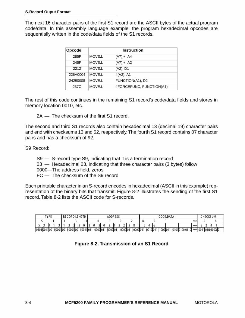
S-Record Ouput Format
8-4
MCF5200 FAMILY PROGRAMMER’S REFERENCE MANUAL
MOTOROLA
The next 16 character pairs of the first S1 record are the ASCII bytes of the actual programcode/data. In this assembly language example, the program hexadecimal opcodes aresequentially written in the code/data fields of the S1 records.
The rest of this code continues in the remaining S1 record’s code/data fields and stores inmemory location 0010, etc.
2A — The checksum of the first S1 record.
The second and third S1 records also contain hexadecimal 13 (decimal 19) character pairsand end with checksums 13 and 52, respectively. The fourth S1 record contains 07 characterpairs and has a checksum of 92.
S9 Record:
S9 — S-record type S9, indicating that it is a termination record03 — Hexadecimal 03, indicating that three character pairs (3 bytes) follow 0000—The address field, zeros FC — The checksum of the S9 record
Each printable character in an S-record encodes in hexadecimal (ASCII in this example) rep-resentation of the binary bits that transmit. Figure 8-2 illustrates the sending of the first S1record. Table 8-2 lists the ASCII code for S-records.
Opcode Instruction
285F MOVE.L (A7) +, A4
245F MOVE.L (A7) +, A2
2212 MOVE.L (A2), D1
226A0004 MOVE.L 4(A2), A1
24290008 MOVE.L FUNCTION(A1), D2
237C MOVE.L #FORCEFUNC, FUNCTION(A1)
Figure 8-2. Transmission of an S1 Record
0101 0011 0011 0001 0011 0001 0011 0011 0011 0000 0011 0000 0011 0000 0011 0000 0011 0010 0011 1000 0011 0101 0100 0110 **** 0011 0010 0100 0001 5 3 3 1 3 1 3 3 3 0 3 0 3 0 3 0 3 2 3 8 3 5 4 6 **** 3 2 4 1
S 1 1 3 0 0 0 0 2 8 5 F **** 2 A RECORD LENGTH ADDRESS CODE/DATA CHECKSUM TYPE

S-Record Output Format
MOTOROLA
MCF5200 FAMILY PROGRAMMER’S REFERENCE MANUAL
8-5
Table 8-2. ASCII Code
LeastSignificant
Digit
Most Significant Digit
0 1 2 3 4 5 6 7
0 NUL DLE SP 0 @ P ‘ p
1 SOH DC1 ! 1 A Q a q
2 STX DC2 “ 2 B R b r
3 ETX DC3 # 3 C S c s
4 EOT DC4 $ 4 D T d t
5 ENQ NAK % 5 E U e u
6 ACK SYN & 6 F V f v
7 BEL ETB ’ 7 G W g w
8 BS CAN ( 8 H X h x
9 HT EM ) 9 I Y i y
A LF SUB * : J Z j z
B VT ESC + ; K [ k {
C FF FS , < L \ l |
D CR GS – = M ] m }
E SO RS . > N ^ n ~
F SI US / ? O _ o DEL

S-Record Ouput Format
8-6
MCF5200 FAMILY PROGRAMMER’S REFERENCE MANUAL
MOTOROLA

MOTOROLA
MCF5200 FAMILY PROGRAMMER’S REFERENCE MANUAL
9-1
SECTION 9INSTRUCTION EXECUTION TIMING (5200 SERIES ONLY)
This section presents ColdFire 5200 Series processor instruction execution times in termsof processor core clock cycles. The number of operand references for each instruction isalso included, enclosed in parentheses following the number of clock cycles. Each timingentry is presented as
C
(r/w) where:
•
C
- The number of processor clock cycles, including all applicable operand fetches and writes, as well as all internal core cycles required to complete the instruction execution.
• r/w - The number of operand reads (r) and writes (w) required by the instruction. An op-eration performing a read-modify-write function is denoted as (1/1).
This section includes assumptions concerning the timing values and the execution timedetails.
9.1 TIMING ASSUMPTIONS
The timing data presented in this section have the following assumptions:
1. The operand execution pipeline (OEP) is loaded with the opword and all required ex-tension words at the beginning of each instruction execution. This implies that the OEP doesn’t wait for the instruction fetch pipeline (IFP) to supply opwords and/or extension words.
2. The OEP does not experience any sequence-related pipeline stalls. For the ColdFire processor, the most common example of this type of stall involves consecutive STORE operations, excluding the MOVEM instruction. For all STORE operations (ex-cept MOVEM), certain hardware resources within the ColdFire processor are marked as "busy" for two clock cycles after the final DSOC cycle of the STORE instruction. If a subsequent STORE instruction is encountered within this 2-cycle window, it will be stalled until the resource again becomes available. Thus, the maximum pipeline stall involving consecutive STORE operations is 2 cycles. The MOVEM instruction uses a different set of resources and this stall does not apply.
3. The OEP completes all memory accesses without any stall conditions caused by the memory itself. Thus, the timing details provided in this section assume an infinite zero-wait state memory is attached to the processor core.
4. All operand data accesses are aligned on the same byte boundary as the operand size: 16-bit operands aligned on 0-modulo-2 addresses, 32-bit operands aligned on 0-modulo-4 addresses.

Instruction Execution Timing
9-2
MCF5200 FAMILY PROGRAMMER’S REFERENCE MANUAL
MOTOROLA
If the operand alignment fails these guidelines, the optional hardware module that supportsmisaligned references is required. With the support this module provides, each misalignedreference requires a minimum of 2 additional clock cycles to process.
9.2 MOVE INSTRUCTION EXECUTION TIMES
The execution times for the MOVE.{B,W} instructions are shown in Table 9-1, while Table9-2 provides the timing for MOVE.L.
For all
tables in this section, the execution time (ET) of any instruction using the PC-relativeeffective addressing modes is exactly equivalent to the time using the comparable An-rela-tive mode.
The nomenclature "xxx.wl" refers to both forms of absolute addressing, xxx.w and xxx.l.
Table 9-1. Move Byte and Word Execution Times
SourceDestination
Rx (Ax) (Ax)+ -(Ax) (d16,Ax) (d8,Ax,Xn*SF) xxx.wl
Dy 1(0/0) 1(0/1) 1(0/1) 1(0/1) 1(0/1) 2(0/1) 1(0/1)Ay 1(0/0) 1(0/1) 1(0/1) 1(0/1) 1(0/1) 2(0/1) 1(0/1)
(Ay) 3(1/0) 3(1/1) 3(1/1) 3(1/1) 3(1/1) 4(1/1) 3(1/1)(Ay)+ 3(1/0) 3(1/1) 3(1/1) 3(1/1) 3(1/1) 4(1/1) 3(1/1)-(Ay) 3(1/0) 3(1/1) 3(1/1) 3(1/1) 3(1/1) 4(1/1) 3(1/1)
(d16,Ay) 3(1/0) 3(1/1) 3(1/1) 3(1/1) 3(1/1) — —(d8,Ay,Xn*SF) 4(1/0) 4(1/1) 4(1/1) 4(1/1) — — —
xxx.w 3(1/0) 3(1/1) 3(1/1) 3(1/1) — — —xxx.l 3(1/0) 3(1/1) 3(1/1) 3(1/1) — — —
(d16,PC) 3(1/0) 3(1/1) 3(1/1) 3(1/1) 3(1/1) — —(d8,PC,Xn*SF) 4(1/0) 4(1/1) 4(1/1) 4(1/1) — — —
#xxx 1(0/0) 3(0/1) 3(0/1) 3(0/1) — — —
Table 9-2. Move Long Execution Times
SourceDestination
Rx (Ax) (Ax)+ -(Ax) (d16,Ax) (d8,Ax,Xn*SF) xxx.wl
Dy 1(0/0) 1(0/1) 1(0/1) 1(0/1) 1(0/1) 2(0/1) 1(0/1)Ay 1(0/0) 1(0/1) 1(0/1) 1(0/1) 1(0/1) 2(0/1) 1(0/1)
(Ay) 2(1/0) 2(1/1) 2(1/1) 2(1/1) 2(1/1) 3(1/1) 2(1/1)(Ay)+ 2(1/0) 2(1/1) 2(1/1) 2(1/1) 2(1/1) 3(1/1) 2(1/1)-(Ay) 2(1/0) 2(1/1) 2(1/1) 2(1/1) 2(1/1) 3(1/1) 2(1/1)
(d16,Ay) 2(1/0) 2(1/1) 2(1/1) 2(1/1) 2(1/1) — —(d8,Ay,Xn*SF) 3(1/0) 3(1/1) 3(1/1) 3(1/1) — — —
xxx.w 2(1/0) 2(1/1) 2(1/1) 2(1/1) — — —xxx.l 2(1/0) 2(1/1) 2(1/1) 2(1/1) — — —
(d16,PC) 2(1/0) 2(1/1) 2(1/1) 2(1/1) 2(1/1) — —(d8,PC,Xn*SF) 3(1/0) 3(1/1) 3(1/1) 3(1/1) — — —
#xxx 1(0/0) 2(0/1) 2(0/1) 2(0/1) — — —
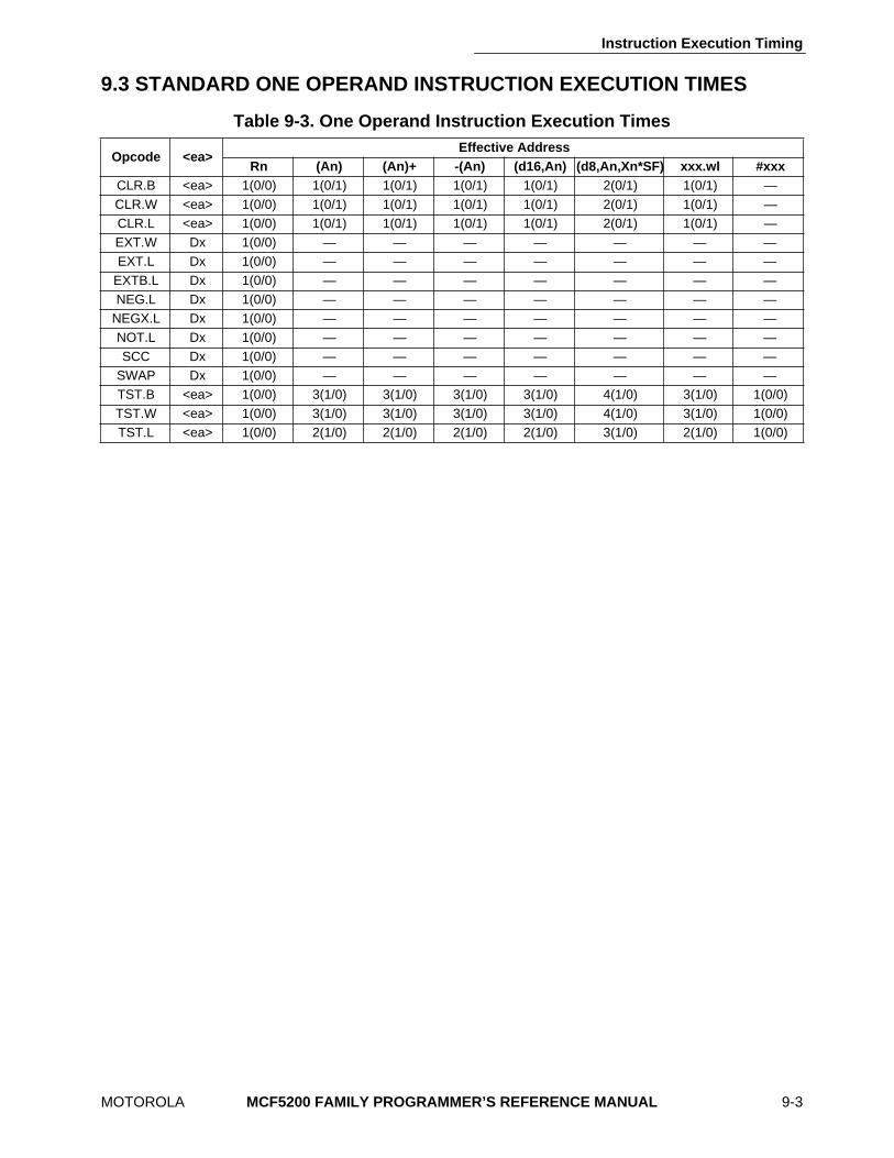
Instruction Execution Timing
MOTOROLA
MCF5200 FAMILY PROGRAMMER’S REFERENCE MANUAL
9-3
9.3 STANDARD ONE OPERAND INSTRUCTION EXECUTION TIMES
Table 9-3. One Operand Instruction Execution Times
Opcode <ea>Effective Address
Rn (An) (An)+ -(An) (d16,An) (d8,An,Xn*SF) xxx.wl #xxx
CLR.B <ea> 1(0/0) 1(0/1) 1(0/1) 1(0/1) 1(0/1) 2(0/1) 1(0/1) —CLR.W <ea> 1(0/0) 1(0/1) 1(0/1) 1(0/1) 1(0/1) 2(0/1) 1(0/1) —CLR.L <ea> 1(0/0) 1(0/1) 1(0/1) 1(0/1) 1(0/1) 2(0/1) 1(0/1) —EXT.W Dx 1(0/0) — — — — — — —EXT.L Dx 1(0/0) — — — — — — —
EXTB.L Dx 1(0/0) — — — — — — —NEG.L Dx 1(0/0) — — — — — — —
NEGX.L Dx 1(0/0) — — — — — — —NOT.L Dx 1(0/0) — — — — — — —SCC Dx 1(0/0) — — — — — — —
SWAP Dx 1(0/0) — — — — — — —TST.B <ea> 1(0/0) 3(1/0) 3(1/0) 3(1/0) 3(1/0) 4(1/0) 3(1/0) 1(0/0)TST.W <ea> 1(0/0) 3(1/0) 3(1/0) 3(1/0) 3(1/0) 4(1/0) 3(1/0) 1(0/0)TST.L <ea> 1(0/0) 2(1/0) 2(1/0) 2(1/0) 2(1/0) 3(1/0) 2(1/0) 1(0/0)

Instruction Execution Timing
9-4
MCF5200 FAMILY PROGRAMMER’S REFERENCE MANUAL
MOTOROLA
9.4 STANDARD TWO OPERAND INSTRUCTION EXECUTION TIMES
Table 9-4. Two Operand Instruction Execution Times
Opcode <ea>Effective Address
Rn (An) (An)+ -(An)(d16,An)(d16,PC)
(d8,An,Xn*SF)(d8,PC,Xn*SF)
xxx.wl #xxx
ADD.L <ea>,Rx 1(0/0) 3(1/0) 3(1/0) 3(1/0) 3(1/0) 4(1/0) 3(1/0) 1(0/0)ADD.L Dy,<ea> — 3(1/1) 3(1/1) 3(1/1) 3(1/1) 4(1/1) 3(1/1) —ADDI.L #imm,Dx 1(0/0) — — — — — — —ADDQ.L #imm,<ea> 1(0/0) 3(1/1) 3(1/1) 3(1/1) 3(1/1) 4(1/1) 3(1/1) —ADDX.L Dy,Dx 1(0/0) — — — — — — —AND.L <ea>,Dn 1(0/0) 3(1/0) 3(1/0) 3(1/0) 3(1/0) 4(1/0) 3(1/0) 1(0/0)AND.L Dy,<ea> — 3(1/1) 3(1/1) 3(1/1) 3(1/1) 4(1/1) 3(1/1) —ANDI.L #imm,Dx 1(0/0) — — — — — — —ASL.L <ea>,Dx 1(0/0) — — — — — — 1(0/0)ASR.L <ea>,Dx 1(0/0) — — — — — — 1(0/0)BCHG Dy,<ea> 2(0/0) 3(1/1) 3(1/1) 3(1/1) 3(1/1) 4(1/1) 3(1/1) —BCHG #imm,<ea> 2(0/0) 3(1/1) 3(1/1) 3(1/1) 3(1/1) — — —BCLR Dy,<ea> 2(0/0) 3(1/1) 3(1/1) 3(1/1) 3(1/1) 4(1/1) 3(1/1) —BCLR #imm,<ea> 2(0/0) 3(1/1) 3(1/1) 3(1/1) 3(1/1) — — —BSET Dy,<ea> 2(0/0) 3(1/1) 3(1/1) 3(1/1) 3(1/1) 4(1/1) 3(1/1) —BSET #imm,<ea> 2(0/0) 3(1/1) 3(1/1) 3(1/1) 3(1/1) — — —BTST Dy,<ea> 2(0/0) 3(1/1) 3(1/1) 3(1/1) 3(1/1) 4(1/1) 3(1/1) —BTST #imm,<ea> 1(0/0) 3(1/1) 3(1/1) 3(1/1) 3(1/1) — — 1(0/0)CMP.L <ea>,Rx 1(0/0) 3(1/0) 3(1/0) 3(1/0) 3(1/0) 4(1/0) 3(1/0) 1(0/0)CMPI.L #imm,Dx 1(0/0) — — — — — — —EOR.L Dy,<ea> 1(0/0) 3(1/1) 3(1/1) 3(1/1) 3(1/1) 4(1/1) 3(1/1) —EORI.L #imm,Dx 1(0/0) — — — — — — —
LEA <ea>,Ax — 1(0/0) — — 1(0/0) 2(0/0) 1(0/0) —LSL.L <ea>,Dx 1(0/0) — — — — — — 1(0/0)LSR.L <ea>,Dx 1(0/0) — — — — — — 1(0/0)
MOVEQ #imm,Dx — — — — — — — 1(0/0)MULS.W <ea>,Dx 9(0/0) 11(1/0) 11(1/0) 11(1/0) 11(1/0) 12(1/0) 11(1/0) 9(0/0)MULU.W <ea>,Dx 9(0/0) 11(1/0) 11(1/0) 11(1/0) 11(1/0) 12(1/0) 11(1/0) 9(0/0)MULS.L <ea>,Dx 18(0/0) 20(1/0) 20(1/0) 20(1/0) 20(1/0) — — —MULU.L <ea>,Dx 18(0/0) 20(1/0) 20(1/0) 20(1/0) 20(1/0) — — —
OR.L <ea>,Dn 1(0/0) 3(1/0) 3(1/0) 3(1/0) 3(1/0) 4(1/0) 3(1/0) 1(0/0)OR.L Dy,<ea> — 3(1/1) 3(1/1) 3(1/1) 3(1/1) 4(1/1) 3(1/1) —OR.L #imm,Dx 1(0/0) — — — — — — —SUB.L <ea>,Rx 1(0/0) 3(1/0) 3(1/0) 3(1/0) 3(1/0) 4(1/0) 3(1/0) 1(0/0)SUB.L Dy,<ea> — 3(1/1) 3(1/1) 3(1/1) 3(1/1) 4(1/1) 3(1/1) —SUBI.L #imm,Dx 1(0/0) — — — — — — —SUBQ.L #imm,<ea> 1(0/0) 3(1/1) 3(1/1) 3(1/1) 3(1/1) 4(1/1) 3(1/1) —SUBX.L Dy,Dx 1(0/0) — — — — — — —

Instruction Execution Timing
MOTOROLA
MCF5200 FAMILY PROGRAMMER’S REFERENCE MANUAL
9-5
9.5 MISCELLANEOUS INSTRUCTION EXECUTION TIMES
Table 9-5. Miscellaneous Instruction Execution Times
Opcode <ea>Effective Address
Rn (An) (An)+ -(An) (d16,An) (d8,An,Xn*SF) xxx.wl #xxx
LINK.W Ay,#imm 2(0/1) — — — — — — —MOVE.W CCR,Dx 1(0/0) — — — — — — —MOVE.W <ea>,CCR 1(0/0) — — — — — — 1(0/0)MOVE.W SR,Dx 1(0/0) — — — — — — —
MOVE.W <ea>,SR 7(0/0) — — — — — — 7(0/0)
1
MOVEC Ry,Rc 9(0/1) — — — — — — —MOVEM.L <ea>,&list — 1+n(n/0) — — 1+n(n/0) — — —MOVEM.L &list,<ea> — 1+n(0/n) — — 1+n(0/n) — — —
NOP 3(0/0) — — — — — — —
PEA <ea> — 2(0/1) — — 2(0/1)
3
3(0/1)
4
2(0/1) —
PULSE 1(0/0) — — — — — — —
STOP #imm — — — — — — — 3(0/0)
2
TRAP #imm — — — — — — — 15(1/2)TPF 1(0/0) — — — — — — —
TPF.W #imm 1(0/0) — — — — — — —TPF.L #imm 1(0/0) — — — — — — —UNLK Ax 2(1/0) — — — — — — —
WDDATA <ea> — 3(1/0) 3(1/0) 3(1/0) 3(1/0) 4(1/0) 3(1/0) 3(1/0)WDEBUG <ea> — 5(2/0) — — 5(2/0) — — —
n is the number of registers moved by the movem opcode.
1
If a MOVE.W #imm,SR instruction is executed and imm[13] = 1, the execution time is 1(0/0).
2
The execution time for STOP is the time required until the processor begins sampling continuously for interrupts.
3
PEA execution times are the same for (d16,PC)
4
PEA execution times are the same for (d8,PC,Xn*SF)

Instruction Execution Timing
9-6
MCF5200 FAMILY PROGRAMMER’S REFERENCE MANUAL
MOTOROLA
9.6 BRANCH INSTRUCTION EXECUTION TIMES
Table 9-6. General Branch Instruction Execution Times
Opcode <ea>Effective Address
Rn (An) (An)+ -(An) (d16,An) (d8,An,Xi*SF) xxx.wl #xxx
BSR — — — — 3(0/1) — — —JMP <ea> — 3(0/0) — — 3(0/0) 4(0/0) 3(0/0) —JSR <ea> — 3(0/1) — — 3(0/1) 4(0/1) 3(0/1) —RTE — — 8(2/0) — — — — —RTS — — 5(1/0) — — — — —
Table 9-7. BRA, Bcc Instruction Execution Times
OpcodeForwardTaken
ForwardNot Taken
BackwardTaken
BackwardNot Taken
BRA 2(0/0) — 2(0/0) —Bcc 3(0/0) 1(0/0) 2(0/0) 3(0/0)

MOTOROLA
MCF5200 FAMILY PROGRAMMER’S REFERENCE MANUAL
A-1
APPENDIX APROCESSOR INSTRUCTION SUMMARY
This appendix provides a quick reference of the ColdFire instructions. Table A-1 lists theColdFire instructions by mnemonics, followed by the descriptive name.
Table A-1. ColdFire Instruction Set
Mnemonic Description
ADD Add ADDA Add Address ADDI Add Immediate ADDQ Add Quick ADDX Add with Extend AND Logical AND ANDI Logical AND Immediate ASL, ASR Arithmetic Shift Left and Right Bcc Branch Conditionally BCHG Test Bit and Change BCLR Test Bit and Clear BRA Branch BSET Test Bit and Set BSR Branch to Subroutine BTST Test BitCLR Clear CMP Compare CMPA Compare Address CMPI Compare ImmediateEOR Logical Exclusive-OR EORI Logical Exclusive-OR Immediate EXT, EXTB Sign ExtendHALT Halt CPUJMP Jump JSR Jump to Subroutine LEA Load Effective Address LINK Link and Allocate LSL, LSR Logical Shift Left and Right MOVE Move MOVEA Move AddressMOVEC Move Control RegisterMOVE from CCR Move from Condition Code Register MOVE to CCR Move to Condition Code Register MOVEM Move Multiple Registers MOVE from SR Move from the Status Register

Appendix A
A-2
MCF5200 FAMILY PROGRAMMER’S REFERENCE MANUAL
MOTOROLA
MOVE to SR Move to the Status RegisterMOVEQ Move QuickMULS Signed Multiply MULU Unsigned Multiply NEG Negate NEGX Negate with Extend NOP No Operation NOT Logical Complement OR Logical Inclusive-OR ORI Logical Inclusive-OR Immediate PEA Push Effective Address PULSE Generate Processor StatusRTE
RTS
Return from Exception
Return from SubroutineSUB Subtract Scc Set According to ConditionSTOP Load Status Register and StopSUBA Subtract Address SUBI Subtract Immediate SUBQ Subtract Quick SUBX Subtract with Extend SWAP Swap Register Words TRAP Trap TRAPF No OperationTST Test Operand UNLK UnlinkWDDATA Write Data Control RegisterWDEBUG Write Debug Control Register
Table A-1. ColdFire Instruction Set (Continued)
Mnemonic Description